

Page 1

MAX V CPLD Development Kit User Guide
MAX V CPLD Development Kit
User Guide
101 Innovation Drive
San Jose, CA 95134
www.altera.com
UG-01099-1.0
Subscribe
Page 2

Copyright © 2011 Altera Corporation. All rights reserved. Altera, The Programmable Solutions Company, the stylized Altera logo, and specific device designations
are trademarks and/or service marks of Altera Corporation in the U.S. and other countries. All other words and logos identified as trademarks and/or service marks
are the property of Altera Corporation or their respective owners. Altera products are protected under numerous U.S. and foreign patents and pending applications,
maskwork rights, and copyrights. Altera warrants performance of its semiconductor products to current specifications in accordance with Altera's standard
warranty, but reserves the right to make changes to any products and services at any time without notice. Altera assumes no responsibility or liability arising out of
the application or use of any information, product, or service described herein except as expressly agreed to in writing by Altera. Altera customers are advised to
obtain the latest version of device specifications before relying on any published information and before placing orders for products or services.
MAX V CPLD Development Kit User Guide January 2011 Altera Corporation
Page 3

Contents
Chapter 1. About This Kit
Kit Features . . . . . . . . . . . . . . . . . . . . . . . . . . . . . . . . . . . . . . . . . . . . . . . . . . . . . . . . . . . . . . . . . . . . . . . . . . . . 1–1
Hardware . . . . . . . . . . . . . . . . . . . . . . . . . . . . . . . . . . . . . . . . . . . . . . . . . . . . . . . . . . . . . . . . . . . . . . . . . . . . 1–1
Software . . . . . . . . . . . . . . . . . . . . . . . . . . . . . . . . . . . . . . . . . . . . . . . . . . . . . . . . . . . . . . . . . . . . . . . . . . . . . 1–2
Quartus II Web Edition Software . . . . . . . . . . . . . . . . . . . . . . . . . . . . . . . . . . . . . . . . . . . . . . . . . . . . . 1–2
MAX V CPLD Development Kit Installer . . . . . . . . . . . . . . . . . . . . . . . . . . . . . . . . . . . . . . . . . . . . . . 1–3
Chapter 2. Getting Started
Before You Begin . . . . . . . . . . . . . . . . . . . . . . . . . . . . . . . . . . . . . . . . . . . . . . . . . . . . . . . . . . . . . . . . . . . . . . . . 2–1
Inspect the Board . . . . . . . . . . . . . . . . . . . . . . . . . . . . . . . . . . . . . . . . . . . . . . . . . . . . . . . . . . . . . . . . . . . . . 2–1
References . . . . . . . . . . . . . . . . . . . . . . . . . . . . . . . . . . . . . . . . . . . . . . . . . . . . . . . . . . . . . . . . . . . . . . . . . . . . . . 2–1
Chapter 3. Software Installation
Installing the Quartus II Web Edition Software . . . . . . . . . . . . . . . . . . . . . . . . . . . . . . . . . . . . . . . . . . . . . . 3–1
Licensing Considerations . . . . . . . . . . . . . . . . . . . . . . . . . . . . . . . . . . . . . . . . . . . . . . . . . . . . . . . . . . . . . . 3–1
Installing the MAX V CPLD Development Kit . . . . . . . . . . . . . . . . . . . . . . . . . . . . . . . . . . . . . . . . . . . . . . . 3–1
Installing the USB-Blaster Driver . . . . . . . . . . . . . . . . . . . . . . . . . . . . . . . . . . . . . . . . . . . . . . . . . . . . . . . . . . 3–2
Chapter 4. Development Board Setup
Setting Up the Board . . . . . . . . . . . . . . . . . . . . . . . . . . . . . . . . . . . . . . . . . . . . . . . . . . . . . . . . . . . . . . . . . . . . . 4–1
Chapter 5. Board Test System
Running the Board Test System . . . . . . . . . . . . . . . . . . . . . . . . . . . . . . . . . . . . . . . . . . . . . . . . . . . . . . . . . . . 5–1
Using the Board Test System . . . . . . . . . . . . . . . . . . . . . . . . . . . . . . . . . . . . . . . . . . . . . . . . . . . . . . . . . . . . . . 5–2
The Config Menu . . . . . . . . . . . . . . . . . . . . . . . . . . . . . . . . . . . . . . . . . . . . . . . . . . . . . . . . . . . . . . . . . . . . . 5–2
The GPIO Tab . . . . . . . . . . . . . . . . . . . . . . . . . . . . . . . . . . . . . . . . . . . . . . . . . . . . . . . . . . . . . . . . . . . . . . . . 5–2
User LEDs . . . . . . . . . . . . . . . . . . . . . . . . . . . . . . . . . . . . . . . . . . . . . . . . . . . . . . . . . . . . . . . . . . . . . . . . . 5–3
Push Buttons . . . . . . . . . . . . . . . . . . . . . . . . . . . . . . . . . . . . . . . . . . . . . . . . . . . . . . . . . . . . . . . . . . . . . . . 5–3
Capacitor Sense Button . . . . . . . . . . . . . . . . . . . . . . . . . . . . . . . . . . . . . . . . . . . . . . . . . . . . . . . . . . . . . . 5–3
The Power Tab . . . . . . . . . . . . . . . . . . . . . . . . . . . . . . . . . . . . . . . . . . . . . . . . . . . . . . . . . . . . . . . . . . . . . . . 5–4
Power Consumption Calculations . . . . . . . . . . . . . . . . . . . . . . . . . . . . . . . . . . . . . . . . . . . . . . . . . . . . 5–5
Power Tab Controls . . . . . . . . . . . . . . . . . . . . . . . . . . . . . . . . . . . . . . . . . . . . . . . . . . . . . . . . . . . . . . . . . 5–5
The Counter Tab . . . . . . . . . . . . . . . . . . . . . . . . . . . . . . . . . . . . . . . . . . . . . . . . . . . . . . . . . . . . . . . . . . . . . . 5–6
The UFM Tab . . . . . . . . . . . . . . . . . . . . . . . . . . . . . . . . . . . . . . . . . . . . . . . . . . . . . . . . . . . . . . . . . . . . . . . . . 5–7
The OSC Tab . . . . . . . . . . . . . . . . . . . . . . . . . . . . . . . . . . . . . . . . . . . . . . . . . . . . . . . . . . . . . . . . . . . . . . . . . 5–8
Internal MAX V Oscillator . . . . . . . . . . . . . . . . . . . . . . . . . . . . . . . . . . . . . . . . . . . . . . . . . . . . . . . . . . . 5–8
Current Value . . . . . . . . . . . . . . . . . . . . . . . . . . . . . . . . . . . . . . . . . . . . . . . . . . . . . . . . . . . . . . . . . . . . . . 5–8
Minimum Observed Value . . . . . . . . . . . . . . . . . . . . . . . . . . . . . . . . . . . . . . . . . . . . . . . . . . . . . . . . . . . 5–8
Maximum Observed Value . . . . . . . . . . . . . . . . . . . . . . . . . . . . . . . . . . . . . . . . . . . . . . . . . . . . . . . . . . 5–9
Reset . . . . . . . . . . . . . . . . . . . . . . . . . . . . . . . . . . . . . . . . . . . . . . . . . . . . . . . . . . . . . . . . . . . . . . . . . . . . . . 5–9
The Speaker Tab . . . . . . . . . . . . . . . . . . . . . . . . . . . . . . . . . . . . . . . . . . . . . . . . . . . . . . . . . . . . . . . . . . . . . 5–10
Volume . . . . . . . . . . . . . . . . . . . . . . . . . . . . . . . . . . . . . . . . . . . . . . . . . . . . . . . . . . . . . . . . . . . . . . . . . . 5–10
Music Notes . . . . . . . . . . . . . . . . . . . . . . . . . . . . . . . . . . . . . . . . . . . . . . . . . . . . . . . . . . . . . . . . . . . . . . 5–10
The Motor Tab . . . . . . . . . . . . . . . . . . . . . . . . . . . . . . . . . . . . . . . . . . . . . . . . . . . . . . . . . . . . . . . . . . . . . . . 5–11
The I2C EEPROM Tab . . . . . . . . . . . . . . . . . . . . . . . . . . . . . . . . . . . . . . . . . . . . . . . . . . . . . . . . . . . . . . . . 5–12
Address Display . . . . . . . . . . . . . . . . . . . . . . . . . . . . . . . . . . . . . . . . . . . . . . . . . . . . . . . . . . . . . . . . . . . 5–12
Write . . . . . . . . . . . . . . . . . . . . . . . . . . . . . . . . . . . . . . . . . . . . . . . . . . . . . . . . . . . . . . . . . . . . . . . . . . . . 5–12
Read . . . . . . . . . . . . . . . . . . . . . . . . . . . . . . . . . . . . . . . . . . . . . . . . . . . . . . . . . . . . . . . . . . . . . . . . . . . . . 5–12
January 2011 Altera Corporation MAX V CPLD Development Kit User Guide
Page 4

iv Contents
The SPI EEPROM Tab . . . . . . . . . . . . . . . . . . . . . . . . . . . . . . . . . . . . . . . . . . . . . . . . . . . . . . . . . . . . . . . . 5–13
Address Display . . . . . . . . . . . . . . . . . . . . . . . . . . . . . . . . . . . . . . . . . . . . . . . . . . . . . . . . . . . . . . . . . . . 5–13
Write . . . . . . . . . . . . . . . . . . . . . . . . . . . . . . . . . . . . . . . . . . . . . . . . . . . . . . . . . . . . . . . . . . . . . . . . . . . . 5–13
Read . . . . . . . . . . . . . . . . . . . . . . . . . . . . . . . . . . . . . . . . . . . . . . . . . . . . . . . . . . . . . . . . . . . . . . . . . . . . . 5–14
Additional Information
Document Revision History . . . . . . . . . . . . . . . . . . . . . . . . . . . . . . . . . . . . . . . . . . . . . . . . . . . . . . . . . . . Info–1
How to Contact Altera . . . . . . . . . . . . . . . . . . . . . . . . . . . . . . . . . . . . . . . . . . . . . . . . . . . . . . . . . . . . . . . . Info–1
Typographic Conventions . . . . . . . . . . . . . . . . . . . . . . . . . . . . . . . . . . . . . . . . . . . . . . . . . . . . . . . . . . . . . Info–1
MAX V CPLD Development Kit User Guide January 2011 Altera Corporation
Page 5

1. About This Kit
The Altera® MAX® V CPLD Development Kit is a complete design environment that
includes both the hardware and software you need to prototype the most common
CPLD applications, including I/O expansion, interface bridging, power management
control, initialization control, and analog interface control. The RoHS-compliant
board, and the license-free Quartus
need to begin developing custom MAX V CPLD designs. The following list describes
what you can accomplish with the kit:
■ Develop designs for the 5M570Z CPLD.
®
II Web Edition software provide everything you
Kit Features
Hardware
■ Measure CPLD power (V
■ Bridge between two different I/O voltages (adjustable V
■ Interface to external functions or devices via four connectors.
■ Read and write to memories:
■ 8-Kbit (Kb) user flash memory (UFM) available within the 5M570Z CPLD.
2
■ I
C or SPI EEPROMs (user installed).
■ Come up to speed quickly with your CPLD design by reusing the example designs
CCINT
and V
CCIO
).
on CPLD Bank 2).
CCIO
provided.
■ Re-use the kit’s PCB board and schematic as a model for your design.
This section briefly describes the MAX V CPLD Development Kit contents.
The MAX V CPLD Development Kit includes the following hardware:
■ MAX V CPLD development board—A development platform that allows you to
develop and prototype hardware designs running on the MAX V 5M570Z CPLD.
f For detailed information about the board components and interfaces, refer
to the MAX V CPLD Development Board Reference Manual.
■ A USB cable to power the board.
■ Embedded USB-Blaster
■ Various user LEDs, push-buttons, and capacitor sense button.
■ Standard PC speaker header.
■ Two direct-current (DC) motor headers.
■ General-purpose I/O connectors to mate with daughtercards.
January 2011 Altera Corporation MAX V CPLD Development Kit User Guide
TM
circuitry for CPLD configuration.
Page 6

1–2 Chapter 1: About This Kit
Kit Features
Software
The software for this kit, described in the following sections, is available on the Altera
website for immediate downloading. You can also request to have Altera mail the
software to you on DVDs.
Quartus II Web Edition Software
The Quartus II Web Edition Software is a license-free set of Altera tools with limited
functionality.
f Download the Quartus II Web Edition Software from the Quartus II Web Edition
Software page of the Altera website. Alternatively, you can request a DVD from the
Altera IP and Software DVD Request Form page of the Altera website.
The Quartus II Web Edition Software includes the following items:
■ Quartus II Software—The Quartus II software, including the SOPC Builder system
development tool, provides a comprehensive environment for
system-on-a-programmable-chip (SOPC) design. The Quartus II software
integrates into nearly any design environment and provides interfaces to
industry-standard EDA tools.
f To compare the Quartus II subscription and web editions, refer to Altera
Quartus II Software — Subscription Edition vs. Web Edition. The kit also works
in conjunction with the subscription edition.
■ MegaCore
®
IP Library—A library that contains Altera IP MegaCore functions. You
can evaluate MegaCore functions by using the OpenCore Plus feature to do the
following:
■ Simulate behavior of a MegaCore function within your system.
■ Verify functionality of your design, and quickly and easily evaluate its size and
speed.
■ Generate time-limited device programming files for designs that include
MegaCore functions.
■ Program a device and verify your design in hardware.
1 The OpenCore Plus hardware evaluation feature is an evaluation tool for
prototyping only. You must purchase a license to use a MegaCore function
in production.
f For more information about OpenCore Plus, refer to AN 320: OpenCore Plus
Evaluation of Megafunctions.
■ Nios
®
II Embedded Design Suite (EDS)—A full-featured set of tools that allows
you to develop embedded software for the Nios II processor which you can
include in your Altera designs.
MAX V CPLD Development Kit User Guide January 2011 Altera Corporation
Page 7

Chapter 1: About This Kit 1–3
Kit Features
MAX V CPLD Development Kit Installer
The license-free MAX V CPLD Development Kit installer includes all the
documentation and design examples for the kit.
Download the MAX V CPLD Development Kit installer from the MAX V CPLD
Development Kit page of the Altera website. Alternatively, you can request a
development kit DVD from the Altera Kit Installations DVD Request Form page of
the Altera website.
January 2011 Altera Corporation MAX V CPLD Development Kit User Guide
Page 8

1–4 Chapter 1: About This Kit
Kit Features
MAX V CPLD Development Kit User Guide January 2011 Altera Corporation
Page 9

The remaining chapters in this user guide lead you through the following MAX V
CPLD development board setup steps:
■ Inspecting the contents of the kit
■ Installing the design and kit software
■ Setting up, powering up, and verifying correct operation of the CPLD
■ Running the Board Test System designs
f For complete information about the CPLD development board, refer to the
MAX V CPLD Development Board Reference Manual.
Before You Begin
Before using the kit or installing the software, check the kit contents and inspect the
board to verify that you received all of the items listed in “Kit Features” on page 1–1.
If any of the items are missing, contact Altera before you proceed.
2. Getting Started
development board
Inspect the Board
References
To inspect the board, perform the following steps:
1. Place the board on an anti-static surface and inspect it to ensure that it has not been
damaged during shipment.
c Without proper anti-static handling, you can damage the board.
2. Verify that all components are on the board and appear intact.
1 The SPI EEPROM (U8) and the I
2
C EEPROM (U6) are not included with the
MAX V CPLD Development Kit.
Use the following links to check the Altera website for other related information:
■ For the latest board design files and reference designs, refer to the MAX V CPLD
Development Kit page.
■ For the MAX V device documentation, refer to the Literature: MAX V Devices
page.
■ To purchase devices from the eStore, refer to the Devices page.
■ For MAX V OrCAD symbols, refer to the Capture CIS Symbols page.
January 2011 Altera Corporation MAX V CPLD Development Kit User Guide
Page 10

2–2 Chapter 2: Getting Started
References
MAX V CPLD Development Kit User Guide January 2011 Altera Corporation
Page 11

This section explains how to install the following software:
■ Quartus II Web Edition Software
■ MAX V CPLD Development Kit
■ USB-Blaster™ driver
Installing the Quartus II Web Edition Software
The Quartus II Web Edition Software provides the necessary tools used for
developing hardware and software for Altera devices. Included in the Quartus II Web
Edition Software are the Quartus II software, the Nios II EDS, and the OpenCore Plus
evaluation IP library. The Quartus II software (including SOPC Builder) and the
Nios II EDS are the primary development tools used to create the reference designs in
this kit. To install the Altera development tools, perform the following steps:
1. Run the Quartus II Web Edition Software installer you acquired in “Software” on
page 1–2.
3. Software Installation
2. Follow the on-screen instructions to complete the installation process.
f If you have difficulty installing the Quartus II software, refer to Altera Software
Installation and Licensing.
Licensing Considerations
The Quartus II Web Edition Software is license-free and supports MAX V devices
without any additional licensing requirement. This kit also works in conjunction with
the Quartus_II Subscription Edition Software, once you obtain the proper license file.
To purchase a subscription, contact your Altera sales representative.
f For complete licensing details, refer to Altera Software Installation and Licensing.
Installing the MAX V CPLD Development Kit
To install the MAX V CPLD Development Kit, perform the following steps:
1. Run the MAX V CPLD Development Kit installer you acquired in “Software” on
page 1–2.
2. Follow the on-screen instructions to complete the installation process. Be sure that
the installation directory you choose is in the same relative location to your
Quartus II software.
January 2011 Altera Corporation MAX V CPLD Development Kit User Guide
Page 12

3–2 Chapter 3: Software Installation
<install dir>
documents
board_design_files
The default Windows installation directory is C:\altera\
<version>
\.
examples
factory_recovery
demos
kits
maxv_5m570z_cpld
Installing the USB-Blaster Driver
The installation program creates the MAX V CPLD Development Kit directory
structure shown in Figure 3–1.
Figure 3–1. MAX V CPLD Development Kit Installed Directory Structure (1)
Note to Figure 3–1:
(1) Early-release versions might have slightly different directory names.
Tab le 3– 1 lists the file directory names and a description of their contents.
Table 3–1. Installed Directory Contents
Directory Name Description of Contents
board_design_files
Contains schematic, layout, assembly, and bill of material board design files. Use these files as a
starting point for a new prototype board design.
demos Contains demonstration applications.
documents Contains the kit documentation.
examples Contains the sample design files for the MAX V CPLD Development Kit.
factory_recovery
Contains the original data programmed onto the board before shipment. Use this data to restore
the board with its original factory contents.
Installing the USB-Blaster Driver
The MAX V CPLD development board includes integrated USB-Blaster circuitry for
device programming. However, for the host computer and board to communicate,
you must install the USB-Blaster driver on the host computer.
f Installation instructions for the USB-Blaster driver for your operating system are
available on the Altera website. On the Altera Programming Cable Driver Information
page of the Altera website, locate the table entry for your configuration and click the
link to access the instructions.
MAX V CPLD Development Kit User Guide January 2011 Altera Corporation
Page 13

The instructions in this chapter explain how to set up the MAX V CPLD development
board.
Setting Up the Board
To prepare and apply power to the board, follow these steps:
1. Ensure that the shunt jumper for J8 (connecting pins 9 and 10) is set to 3.3 V
(default setting).
2. To power up the board, plug in the USB cable to the host PC, and plug the other
end of USB cable into the board USB type B connector (J4). No other power supply
is needed.
When the board is powered up, the blue LED power indicator will illuminate.
1 It is also possible to power up the board through the BATT+ and BATT- connectors
using three 1.5-V batteries in series. However, once you plug in a USB cable, the board
disconnects the battery supply and obtains power from the USB cable.
4. Development Board Setup
January 2011 Altera Corporation MAX V CPLD Development Kit User Guide
Page 14

4–2 Chapter 4: Development Board Setup
Setting Up the Board
MAX V CPLD Development Kit User Guide January 2011 Altera Corporation
Page 15

5. Board Test System
The kit includes a design example and application called the Board Test System to test
the functionality of the MAX V CPLD development board. The application provides
an easy-to-use interface to alter functional settings and observe the results. You can
use the application to test board components, observe performance, and measure
power usage. The application is also useful as a reference for designing systems. To
install the application, follow the steps in “Installing the MAX V CPLD Development
Kit” on page 3–1.
The application provides access to the following MAX V CPLD development board
features:
■ General purpose I/O (GPIO)
■ User flash memory (UFM)
■ Capacitor sense button
■ User LEDs and push buttons
■ Replaceable oscillator
■ Off-chip I
■ Speaker header
■ Two DC motor headers
2
C and SPI EEPROM interfaces
The application allows you to exercise most of the board components. While using the
application, you reconfigure the CPLD several times with test designs specific to the
functionality you are testing.
Several designs are provided to test the major board features. Each design provides
data for one or more tabs in the application. The Config menu identifies the
appropriate design to download to the CPLD for each tab.
After successful CPLD configuration, the appropriate tab appears and allows you to
exercise the related board features. Highlights appear in the board picture around the
corresponding components.
1 The Board Test System shares the JTAG bus with other applications like the Nios II
debugger and the SignalTap
®
II Embedded Logic Analyzer. When the BTS is
connecting to the board, it completely occupies the JTAG bus. If you want to
reconfigure the CPLD through the Quartus II Programmer, be sure to close the BTS
application first.
Running the Board Test System
To run the application, navigate to the
<install dir>\kits\maxv_5m570z_cpld\examples\board_test_system directory and
run the BoardTestSystem.exe application.
1 On Windows, click Start > All Programs > Altera > MAX V CPLD Development Kit
<version> > Board Test System to run the application.
January 2011 Altera Corporation MAX V CPLD Development Kit User Guide
Page 16

5–2 Chapter 5: Board Test System
A GUI appears, displaying the application tab that corresponds to the design running
in the CPLD.
Using the Board Test System
Using the Board Test System
This section describes each control in the Board Test System application.
The Config Menu
Each design example tests a different functionality that corresponds to one or more
application tabs. Use the Config menu to select the design you want to use. Figure 5–1
shows the Config menu.
Figure 5–1. The Config Menu
To configure the CPLD with a test system design, on the Config menu, click the
configure command that corresponds to the functionality you wish to test.
1 While the configuration is running, a progress bar displays. A message shows when
the configuration is completed.
The GPIO Tab
The GPIO tab allows you to interact with all the general purpose user I/O
components on your board.
1 The MAX V CPLD Development Kit includes three designs examples for the GPIO
tab (Figure 5–1):
■ BTS General (VAR_VCCIO = 3.3V) runs when I/O voltage is set to 3.3 V (Bank 2).
■ BTS General (VAR_VCCIO = 2.5V) runs when I/O voltage is set to 2.5 V (Bank 2).
■ BTS General (VAR_VCCIO = 1.8V) runs when I/O voltage is set to 1.8 V (Bank 2).
MAX V CPLD Development Kit User Guide January 2011 Altera Corporation
Page 17

Chapter 5: Board Test System 5–3
Using the Board Test System
Figure 5–2 shows the GPIO tab.
Figure 5–2. The GPIO Tab
The following sections describe the controls on the GPIO tab.
User LEDs
The User LEDs control displays the current state of the user LEDs. Click the LED
buttons to turn the board LEDs on and off.
Push Buttons
The read-only Push Buttons control displays the current state of the board user push
buttons. Press a push button on the board to see the graphical display change
accordingly.
Capacitor Sense Button
The inner circle of the Capacitor Sense Button on the GPIO tab changes to yellow
when you put your finger on the actual capacitor sense button on the board.
January 2011 Altera Corporation MAX V CPLD Development Kit User Guide
Page 18

5–4 Chapter 5: Board Test System
Using the Board Test System
The Power Tab
The Power tab allows you to measure estimated power consumption for the MAX V
through test points available on the development board, as specified by the BTS
General design you choose from the Config menu (Figure 5–1).
f For more information on the location of the test points and details on MAX V rail
voltage, refer to the MAX V CPLD Development Board Reference Manual.
Figure 5–3 shows the Power tab.
Figure 5–3. The Power Tab
1 Follow the on-screen instructions for the measurement steps.
MAX V CPLD Development Kit User Guide January 2011 Altera Corporation
Page 19

Chapter 5: Board Test System 5–5
Using the Board Test System
Power Consumption Calculations
To calculate the estimated power consumption of the 1.8 VCCINT core power, the
Power tab uses the following formulas to arrive at the results after clicking Calculate:
■ Current across Rsense (R44) = Voltage drop across Rsense/Rsense resistance
■ Power consumption of V
= device core voltage (V
CCINT
) × current across
CCINT
Rsense
For example:
Current across Rsense (R44) = (0.756 mV)/(0.27) = 2.8 mA
Power consumption of V
= (1.8 V) × (2.8 mA) = 5.04 mW
CCINT
You can apply the same formulas to the VARIABLE VCCIO power estimation
calculation:
Current across Rsense (R47) = (0.332 mV)/(0.27) = 1.23 mA
Power consumption of V
= (3.3 V) × (1.23 mA) = 4.06 mW
CCIO
Power Tab Controls
The following sections describe the controls on the Power tab.
1.8 VCCINT
■ TP1-TP2—Allows you to enter the value recorded from the multimeter.
■ Result—Shows the calculated power consumption after clicking Calculate.
■ Calculate—Perfoms calculation for estimated power consumption.
VARIABLE VCCIO
■ TP3-TP4—Allows you to enter the value recorded from the multimeter.
■ VA R VC C IO —Allows you to select the voltage level that matches the current
setting on J8 on the development board.
■ Result—Shows the calculated power consumption after clicking Calculate.
■ Calculate—Perfoms calculation for estimated power consumption.
January 2011 Altera Corporation MAX V CPLD Development Kit User Guide
Page 20

5–6 Chapter 5: Board Test System
Using the Board Test System
The Counter Tab
The Counter tab allows you view and control the CPLD counter in a visual display. By
using logic design and the internal oscillator as a counter, this design example shows
the time delay before turning on an LED. (CPLDs are frequently used to monitor and
control power IC’s, such as switchers and regulators.)
Figure 5–4 shows the Counter tab.
Figure 5–4. The Counter Tab
The following sections describe the controls on the Counter tab.
Counter display—Shows number count and highlights a section around the
circumference.
Seconds—Allows you to enter the number of seconds for the counter from 1 to 10.
Start—Begins counter test.
Reset—Sets counter to zero.
MAX V CPLD Development Kit User Guide January 2011 Altera Corporation
Page 21
Chapter 5: Board Test System 5–7
Using the Board Test System
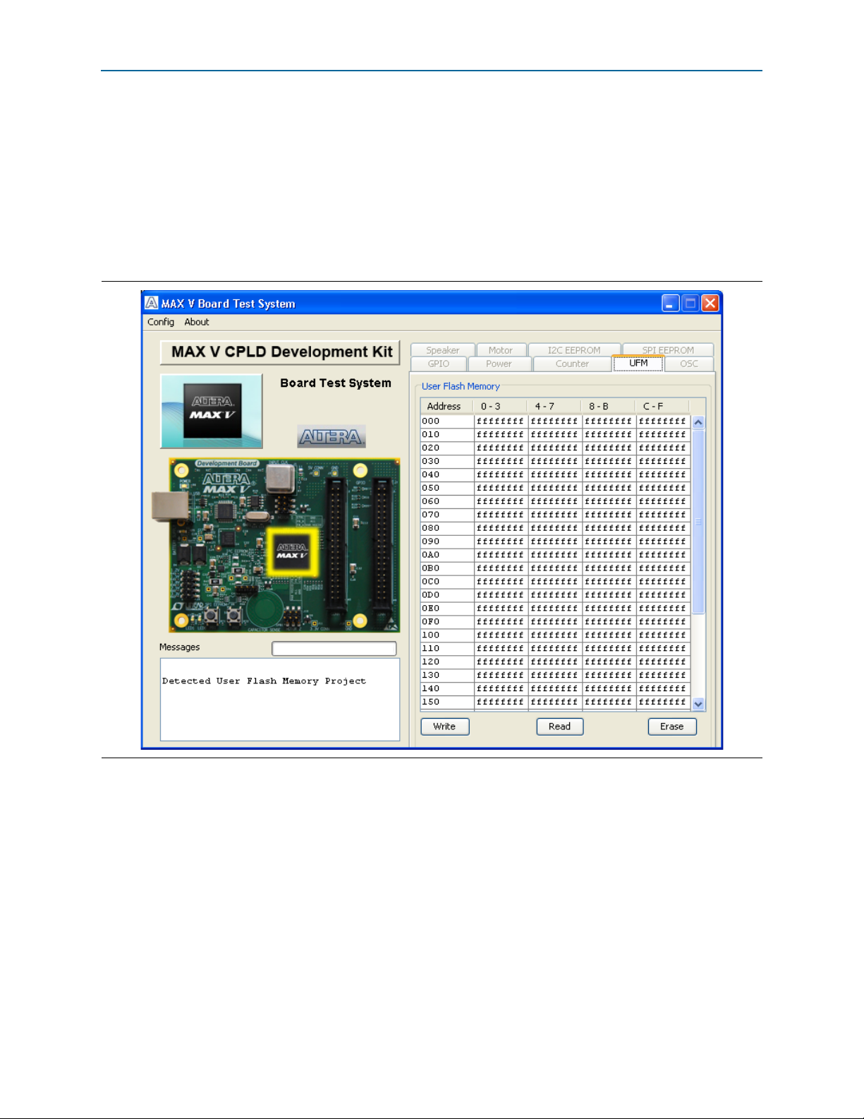
The UFM Tab
The UFM tab displays sector 0 of the user flash memory content (4,096 bits per sector),
and allows you to write, read, and erase the sector 0 address space. Figure 5–5 shows
the UFM tab.
1 MAX V devices feature a single UFM block, which can be used like a serial EEPROM
for storing non-volatile information up to 8,192 bits.
Figure 5–5. The UFM Tab
The following sections describe the controls on the UFM tab.
The table control allows you to type hex values in any cell.
Write—This control writes sector 0 of the UFM.
Read—This control reads sector 0 of the UFM.
Erase—This control erases sector 0 completely.
f For detailed information on UFM storage, refer to the MAX V Device Handbook.
January 2011 Altera Corporation MAX V CPLD Development Kit User Guide
Page 22

5–8 Chapter 5: Board Test System
Using the Board Test System
The OSC Tab
The OSC tab allows you to monitor the current frequency of the MAX V internal
oscillator. Figure 5–6 shows the OSC tab.
Figure 5–6. The OSC Tab
The following sections describe the controls on the OSC tab.
Internal MAX V Oscillator
This diagram shows an internal oscillator symbol from the Block Editor of the
Quartus II software.
Current Value
This control shows the current frequency of the internal oscillator since the test has
been running or since clicking the Reset button. This value is somewhere between 3.3
to 5.3 MHz.
Minimum Observed Value
This control shows the minimum frequency of the internal oscillator since the test has
been running or since clicking the Reset button.
MAX V CPLD Development Kit User Guide January 2011 Altera Corporation
Page 23

Chapter 5: Board Test System 5–9
Using the Board Test System
Maximum Observed Value
This control shows the maximum frequency value since the test has been running or
since clicking the Reset button.
Reset
This control allows you to set the minimum and maximum frequency to the same
value, which is equivalent to starting the test.
January 2011 Altera Corporation MAX V CPLD Development Kit User Guide
Page 24

5–10 Chapter 5: Board Test System
Using the Board Test System
The Speaker Tab
The Speaker tab allows you to play sounds through a standard 4-pin PC speaker, once
the recommended speaker is installed.
1 A speaker is not included with the MAX V CPLD Development Kit.
f For more information on the PC speaker header and manufacturing information, refer
to the MAX V CPLD Development Board Reference Manual.
Figure 5–7 shows the Speaker tab.
Figure 5–7. The Speaker Tab
The following sections describe the controls on the Speaker tab.
Volume
The Vo l um e control allows you to adjust the volume in three steps.
Music Notes
The Music Notes control allows you play the notes in a single octave through an
external 4-pin speaker.
MAX V CPLD Development Kit User Guide January 2011 Altera Corporation
Page 25

Chapter 5: Board Test System 5–11
Using the Board Test System
The Motor Tab
The Motor tab allows you to control and monitor DC motor speed once the
recommended motor is properly installed.
1 A motor is not included with the MAX V CPLD Development Kit.
f For more information on the recommended DC motor and manufacturing
information, refer to the MAX V CPLD Development Board Reference Manual.
Figure 5–8 shows the Motor tab.
Figure 5–8. The Motor Tab
The following sections describe the controls on the Motor tab.
rpm—Shows the actual rotor speed in rpm as effected by the following buttons:
Slow—Slows the rotor speed to between 65 and 75 rpm.
Normal—Sets the rotor speed to between 130 and 140 rpm.
Fast—Increases the rotor speed to between 190 and 200 rpm.
January 2011 Altera Corporation MAX V CPLD Development Kit User Guide
Page 26

5–12 Chapter 5: Board Test System
Using the Board Test System
The I2C EEPROM Tab
This tab (Figure 5–6) allows you to read and write 1 Kb to a user self-mounted I2C
EEPROM located at U6 on the development board.
1 EEPROMs are not included with the MAX V CPLD Development Kit. This test is
designed for a Microchip Technology EEPROM in the SOT-23 package. For more
information on the recommended EEPROMS, refer to the MAX V CPLD Development
Board Reference Manual.
Figure 5–9. The I2C EEPROM Tab
The following sections describe the controls on the I2C EEPROM tab.
Address Display
Displays addresses of the I2C EEPROM.
Write
Writes all of the current 1-Kb data to the I2C EEPROM.
Read
Reads all of the current 1-Kb data from the I2C EEPROM.
MAX V CPLD Development Kit User Guide January 2011 Altera Corporation
Page 27

Chapter 5: Board Test System 5–13
Using the Board Test System
The SPI EEPROM Tab
This tab (Figure 5–10) allows you to read and write 1-K data to a user self-mounted
SPI EEPROM located at U6 on the development board.
1 EEPROMs are not included with the MAX V CPLD Development Kit. This test is
designed for a Microchip Technology EEPROM in the TSSOP-8 package. For more
information on the recommended EEPROMS, refer to the MAX V CPLD Development
Board Reference Manual.
Figure 5–10. The SPI EEPROM Tab
The following sections describe the controls on the SPI EEPROM tab.
Address Display
Displays addresses of the SPI EEPROM.
Write
Writes all of the current 1-Kb data to the SPI EEPROM.
January 2011 Altera Corporation MAX V CPLD Development Kit User Guide
Page 28

5–14 Chapter 5: Board Test System
Using the Board Test System
Read
Reads all of the current 1-Kb data from the I2C EEPROM.
MAX V CPLD Development Kit User Guide January 2011 Altera Corporation
Page 29

This chapter provides additional information about the document and Altera.
Document Revision History
The following table shows the revision history for this document.
Date Version Changes
January 2011 1.0 Initial release.
How to Contact Altera
To locate the most up-to-date information about Altera products, refer to the
following table.
Additional Information
Contact (1) Contact Method Address
Technical support Website www.altera.com/support
Technical training
Product literature Website www.altera.com/literature
Non-technical support (General) Email nacomp@altera.com
(Software Licensing) Email authorization@altera.com
Note to Table:
(1) You can also contact your local Altera sales office or sales representative.
Website www.altera.com/training
Email custrain@altera.com
Typographic Conventions
The following table shows the typographic conventions this document uses.
Visual Cue Meaning
Bold Type with Initial Capital
Letters
bold type
Italic Type with Initial Capital Letters Indicate document titles. For example, Stratix IV Design Guidelines.
italic type
Initial Capital Letters
Indicate command names, dialog box titles, dialog box options, and other GUI
labels. For example, Save As dialog box. For GUI elements, capitalization matches
the GUI.
Indicates directory names, project names, disk drive names, file names, file name
extensions, software utility names, and GUI labels. For example, \qdesigns
directory, D: drive, and chiptrip.gdf file.
Indicates variables. For example, n + 1.
Variable names are enclosed in angle brackets (< >). For example, <file name> and
<project name>.pof file.
Indicate keyboard keys and menu names. For example, the Delete key and the
Options menu.
January 2011 Altera Corporation MAX V CPLD Development Kit User Guide
Page 30

Info–2 Chapter :
Typographic Conventions
Visual Cue Meaning
“Subheading Title”
Quotation marks indicate references to sections within a document and titles of
Quartus II Help topics. For example, “Typographic Conventions.”
Indicates signal, port, register, bit, block, and primitive names. For example,
tdi
, and
input
. The suffix n denotes an active-low signal. For example,
data1
resetn
.
Indicates command line commands and anything that must be typed exactly as it
Courier type
appears. For example,
c:\qdesigns\tutorial\chiptrip.gdf
.
Also indicates sections of an actual file, such as a Report File, references to parts of
files (for example, the AHDL keyword
TRI
example,
).
SUBDESIGN
), and logic function names (for
r An angled arrow instructs you to press the Enter key.
1., 2., 3., and
a., b., c., and so on
■ ■ ■ Bullets indicate a list of items when the sequence of the items is not important.
Numbered steps indicate a list of items when the sequence of the items is important,
such as the steps listed in a procedure.
1 The hand points to information that requires special attention.
h A question mark directs you to a software help system with related information.
f The feet direct you to another document or website with related information.
c
w
A caution calls attention to a condition or possible situation that can damage or
destroy the product or your work.
A warning calls attention to a condition or possible situation that can cause you
injury.
The envelope links to the Email Subscription Management Center page of the Altera
website, where you can sign up to receive update notifications for Altera documents.
,
MAX V CPLD Development Kit User Guide January 2011 Altera Corporation
 Loading...