

Page 1

MAX II Device Handbook
101 Innovation Drive
San Jose, CA 95134
www.alter a.com
MII5V1-3.3
Page 2

Copyright © 2009 Altera Corporation. All rights reserved. Altera, The Programmable Solutions Company, the stylized Altera logo, specific device designations, and all other
words and logos that are identified as trademarks and/or service marks are, unless noted otherwise, the trademarks and service marks of Altera Corporation in the U.S. and other
countries. All other product or service names are the property of their respective holders. Altera products are protected under numerous U.S. and foreign patents and pending applications, maskwork rights, and copyrights. Altera warrants performance of its semiconductor products to current specifications in accordance with Altera's standard warranty,
but reserves the right to make changes to any products and services at any time without notice. Altera assumes no responsibility or liability arising out of the application or use of
any information, product, or service described herein except as expressly agreed to in writing by Altera Corporation. Altera customers are advised to obtain the latest version of
device specifications before relying on any published information and before placing orders for products or services
.
Page 3

Contents
Chapter Revision Dates . . . . . . . . . . . . . . . . . . . . . . . . . . . . . . . . . . . . . . . . . . . . . . . . . . . . . . . . . . . . . . . . . . . . . . xi
About this Handbook . . . . . . . . . . . . . . . . . . . . . . . . . . . . . . . . . . . . . . . . . . . . . . . . . . . . . . . . . . . . . . . . .About–xiii
How to Contact Altera . . . . . . . . . . . . . . . . . . . . . . . . . . . . . . . . . . . . . . . . . . . . . . . . . . . . . . . . . . . . . . . . . 1–xiii
Typographic Conventions . . . . . . . . . . . . . . . . . . . . . . . . . . . . . . . . . . . . . . . . . . . . . . . . . . . . . . . . . . . . . . 1–xiii
Section I. MAX II Device Family Data Sheet
Revision History . . . . . . . . . . . . . . . . . . . . . . . . . . . . . . . . . . . . . . . . . . . . . . . . . . . . . . . . . . . . . . . . . . . . . . . . I–1
Chapter 1. Introduction
Introduction . . . . . . . . . . . . . . . . . . . . . . . . . . . . . . . . . . . . . . . . . . . . . . . . . . . . . . . . . . . . . . . . . . . . . . . . . . . . 1–1
Features . . . . . . . . . . . . . . . . . . . . . . . . . . . . . . . . . . . . . . . . . . . . . . . . . . . . . . . . . . . . . . . . . . . . . . . . . . . . . . . . 1–1
Referenced Documents . . . . . . . . . . . . . . . . . . . . . . . . . . . . . . . . . . . . . . . . . . . . . . . . . . . . . . . . . . . . . . . . . . . 1–4
Document Revision History . . . . . . . . . . . . . . . . . . . . . . . . . . . . . . . . . . . . . . . . . . . . . . . . . . . . . . . . . . . . . . 1–4
Chapter 2. MAX II Architecture
Introduction . . . . . . . . . . . . . . . . . . . . . . . . . . . . . . . . . . . . . . . . . . . . . . . . . . . . . . . . . . . . . . . . . . . . . . . . . . . . 2–1
Functional Description . . . . . . . . . . . . . . . . . . . . . . . . . . . . . . . . . . . . . . . . . . . . . . . . . . . . . . . . . . . . . . . . . . . 2–1
Logic Array Blocks . . . . . . . . . . . . . . . . . . . . . . . . . . . . . . . . . . . . . . . . . . . . . . . . . . . . . . . . . . . . . . . . . . . . . . 2–4
LAB Interconnects . . . . . . . . . . . . . . . . . . . . . . . . . . . . . . . . . . . . . . . . . . . . . . . . . . . . . . . . . . . . . . . . . . . . 2–4
LAB Control Signals . . . . . . . . . . . . . . . . . . . . . . . . . . . . . . . . . . . . . . . . . . . . . . . . . . . . . . . . . . . . . . . . . . . 2–5
Logic Elements . . . . . . . . . . . . . . . . . . . . . . . . . . . . . . . . . . . . . . . . . . . . . . . . . . . . . . . . . . . . . . . . . . . . . . . . . . 2–6
LUT Chain and Register Chain . . . . . . . . . . . . . . . . . . . . . . . . . . . . . . . . . . . . . . . . . . . . . . . . . . . . . . . . . . 2–8
addnsub Signal . . . . . . . . . . . . . . . . . . . . . . . . . . . . . . . . . . . . . . . . . . . . . . . . . . . . . . . . . . . . . . . . . . . . . . . 2–8
LE Operating Modes . . . . . . . . . . . . . . . . . . . . . . . . . . . . . . . . . . . . . . . . . . . . . . . . . . . . . . . . . . . . . . . . . . 2–8
Normal Mode . . . . . . . . . . . . . . . . . . . . . . . . . . . . . . . . . . . . . . . . . . . . . . . . . . . . . . . . . . . . . . . . . . . . . . 2–9
Dynamic Arithmetic Mode . . . . . . . . . . . . . . . . . . . . . . . . . . . . . . . . . . . . . . . . . . . . . . . . . . . . . . . . . . . 2–9
Carry-Select Chain . . . . . . . . . . . . . . . . . . . . . . . . . . . . . . . . . . . . . . . . . . . . . . . . . . . . . . . . . . . . . . . . . 2–10
Clear and Preset Logic Control . . . . . . . . . . . . . . . . . . . . . . . . . . . . . . . . . . . . . . . . . . . . . . . . . . . . . . 2–12
MultiTrack Interconnect . . . . . . . . . . . . . . . . . . . . . . . . . . . . . . . . . . . . . . . . . . . . . . . . . . . . . . . . . . . . . . . . . 2–12
Global Signals . . . . . . . . . . . . . . . . . . . . . . . . . . . . . . . . . . . . . . . . . . . . . . . . . . . . . . . . . . . . . . . . . . . . . . . . . 2–16
User Flash Memory Block . . . . . . . . . . . . . . . . . . . . . . . . . . . . . . . . . . . . . . . . . . . . . . . . . . . . . . . . . . . . . . . 2–18
UFM Storage . . . . . . . . . . . . . . . . . . . . . . . . . . . . . . . . . . . . . . . . . . . . . . . . . . . . . . . . . . . . . . . . . . . . . . . . 2–19
Internal Oscillator . . . . . . . . . . . . . . . . . . . . . . . . . . . . . . . . . . . . . . . . . . . . . . . . . . . . . . . . . . . . . . . . . . . . 2–20
Program, Erase, and Busy Signals . . . . . . . . . . . . . . . . . . . . . . . . . . . . . . . . . . . . . . . . . . . . . . . . . . . . . . 2–20
Auto-Increment Addressing . . . . . . . . . . . . . . . . . . . . . . . . . . . . . . . . . . . . . . . . . . . . . . . . . . . . . . . . . . . 2–20
Serial Interface . . . . . . . . . . . . . . . . . . . . . . . . . . . . . . . . . . . . . . . . . . . . . . . . . . . . . . . . . . . . . . . . . . . . . . . 2–20
UFM Block to Logic Array Interface . . . . . . . . . . . . . . . . . . . . . . . . . . . . . . . . . . . . . . . . . . . . . . . . . . . . 2–20
MultiVolt Core . . . . . . . . . . . . . . . . . . . . . . . . . . . . . . . . . . . . . . . . . . . . . . . . . . . . . . . . . . . . . . . . . . . . . . . . . 2–22
© August 2009 Altera Corporation MAX II Device Handbook
Page 4

iv
I/O Structure . . . . . . . . . . . . . . . . . . . . . . . . . . . . . . . . . . . . . . . . . . . . . . . . . . . . . . . . . . . . . . . . . . . . . . . . . . 2–23
Fast I/O Connection . . . . . . . . . . . . . . . . . . . . . . . . . . . . . . . . . . . . . . . . . . . . . . . . . . . . . . . . . . . . . . . . . . 2–23
I/O Blocks . . . . . . . . . . . . . . . . . . . . . . . . . . . . . . . . . . . . . . . . . . . . . . . . . . . . . . . . . . . . . . . . . . . . . . . . . . 2–24
I/O Standards and Banks . . . . . . . . . . . . . . . . . . . . . . . . . . . . . . . . . . . . . . . . . . . . . . . . . . . . . . . . . . . . . 2–26
PCI Compliance . . . . . . . . . . . . . . . . . . . . . . . . . . . . . . . . . . . . . . . . . . . . . . . . . . . . . . . . . . . . . . . . . . . 2–28
Schmitt Trigger . . . . . . . . . . . . . . . . . . . . . . . . . . . . . . . . . . . . . . . . . . . . . . . . . . . . . . . . . . . . . . . . . . . . . . 2–29
Output Enable Signals . . . . . . . . . . . . . . . . . . . . . . . . . . . . . . . . . . . . . . . . . . . . . . . . . . . . . . . . . . . . . . . . 2–29
Programmable Drive Strength . . . . . . . . . . . . . . . . . . . . . . . . . . . . . . . . . . . . . . . . . . . . . . . . . . . . . . . . . 2–29
Slew-Rate Control . . . . . . . . . . . . . . . . . . . . . . . . . . . . . . . . . . . . . . . . . . . . . . . . . . . . . . . . . . . . . . . . . . . . 2–30
Open-Drain Output . . . . . . . . . . . . . . . . . . . . . . . . . . . . . . . . . . . . . . . . . . . . . . . . . . . . . . . . . . . . . . . . . . 2–30
Programmable Ground Pins . . . . . . . . . . . . . . . . . . . . . . . . . . . . . . . . . . . . . . . . . . . . . . . . . . . . . . . . . . . 2–30
Bus Hold . . . . . . . . . . . . . . . . . . . . . . . . . . . . . . . . . . . . . . . . . . . . . . . . . . . . . . . . . . . . . . . . . . . . . . . . . . . 2–31
Programmable Pull-Up Resistor . . . . . . . . . . . . . . . . . . . . . . . . . . . . . . . . . . . . . . . . . . . . . . . . . . . . . . . . 2–31
Programmable Input Delay . . . . . . . . . . . . . . . . . . . . . . . . . . . . . . . . . . . . . . . . . . . . . . . . . . . . . . . . . . . . 2–31
MultiVolt I/O Interface . . . . . . . . . . . . . . . . . . . . . . . . . . . . . . . . . . . . . . . . . . . . . . . . . . . . . . . . . . . . . . . 2–31
Referenced Documents . . . . . . . . . . . . . . . . . . . . . . . . . . . . . . . . . . . . . . . . . . . . . . . . . . . . . . . . . . . . . . . . . . 2–32
Document Revision History . . . . . . . . . . . . . . . . . . . . . . . . . . . . . . . . . . . . . . . . . . . . . . . . . . . . . . . . . . . . . 2–33
Chapter 3. JTAG and In-System Programmability
Introduction . . . . . . . . . . . . . . . . . . . . . . . . . . . . . . . . . . . . . . . . . . . . . . . . . . . . . . . . . . . . . . . . . . . . . . . . . . . . 3–1
IEEE Std. 1149.1 (JTAG) Boundary-Scan Support . . . . . . . . . . . . . . . . . . . . . . . . . . . . . . . . . . . . . . . . . . . . 3–1
JTAG Block . . . . . . . . . . . . . . . . . . . . . . . . . . . . . . . . . . . . . . . . . . . . . . . . . . . . . . . . . . . . . . . . . . . . . . . . . . 3–3
Parallel Flash Loader . . . . . . . . . . . . . . . . . . . . . . . . . . . . . . . . . . . . . . . . . . . . . . . . . . . . . . . . . . . . . . . . 3–3
In System Programmability . . . . . . . . . . . . . . . . . . . . . . . . . . . . . . . . . . . . . . . . . . . . . . . . . . . . . . . . . . . . . . . 3–4
IEEE 1532 Support . . . . . . . . . . . . . . . . . . . . . . . . . . . . . . . . . . . . . . . . . . . . . . . . . . . . . . . . . . . . . . . . . . . . 3–5
Jam Standard Test and Programming Language (STAPL) . . . . . . . . . . . . . . . . . . . . . . . . . . . . . . . . . . 3–5
Programming Sequence . . . . . . . . . . . . . . . . . . . . . . . . . . . . . . . . . . . . . . . . . . . . . . . . . . . . . . . . . . . . . . . . 3–5
UFM Programming . . . . . . . . . . . . . . . . . . . . . . . . . . . . . . . . . . . . . . . . . . . . . . . . . . . . . . . . . . . . . . . . . . . 3–6
In-System Programming Clamp . . . . . . . . . . . . . . . . . . . . . . . . . . . . . . . . . . . . . . . . . . . . . . . . . . . . . . . . . 3–6
Real-Time ISP . . . . . . . . . . . . . . . . . . . . . . . . . . . . . . . . . . . . . . . . . . . . . . . . . . . . . . . . . . . . . . . . . . . . . . . . 3–7
Design Security . . . . . . . . . . . . . . . . . . . . . . . . . . . . . . . . . . . . . . . . . . . . . . . . . . . . . . . . . . . . . . . . . . . . . . . 3–7
Programming with External Hardware . . . . . . . . . . . . . . . . . . . . . . . . . . . . . . . . . . . . . . . . . . . . . . . . . . 3–7
Referenced Documents . . . . . . . . . . . . . . . . . . . . . . . . . . . . . . . . . . . . . . . . . . . . . . . . . . . . . . . . . . . . . . . . . . . 3–7
Document Revision History . . . . . . . . . . . . . . . . . . . . . . . . . . . . . . . . . . . . . . . . . . . . . . . . . . . . . . . . . . . . . . 3–8
Chapter 4. Hot Socketing and Power-On Reset in MAX II Devices
Introduction . . . . . . . . . . . . . . . . . . . . . . . . . . . . . . . . . . . . . . . . . . . . . . . . . . . . . . . . . . . . . . . . . . . . . . . . . . . . 4–1
MAX II Hot-Socketing Specifications . . . . . . . . . . . . . . . . . . . . . . . . . . . . . . . . . . . . . . . . . . . . . . . . . . . . . . . 4–1
Devices Can Be Driven before Power-Up . . . . . . . . . . . . . . . . . . . . . . . . . . . . . . . . . . . . . . . . . . . . . . . . . 4–1
I/O Pins Remain Tri-Stated during Power-Up . . . . . . . . . . . . . . . . . . . . . . . . . . . . . . . . . . . . . . . . . . . . 4–2
Signal Pins Do Not Drive the V
CCIO
or V
Power Supplies . . . . . . . . . . . . . . . . . . . . . . . . . . . . . . . 4–2
CCINT
AC and DC Specifications . . . . . . . . . . . . . . . . . . . . . . . . . . . . . . . . . . . . . . . . . . . . . . . . . . . . . . . . . . . . . . 4–2
Hot Socketing Feature Implementation in MAX II Devices . . . . . . . . . . . . . . . . . . . . . . . . . . . . . . . . . . . . 4–2
Power-On Reset Circuitry . . . . . . . . . . . . . . . . . . . . . . . . . . . . . . . . . . . . . . . . . . . . . . . . . . . . . . . . . . . . . . . . 4–5
Power-Up Characteristics . . . . . . . . . . . . . . . . . . . . . . . . . . . . . . . . . . . . . . . . . . . . . . . . . . . . . . . . . . . . . . 4–6
Referenced Documents . . . . . . . . . . . . . . . . . . . . . . . . . . . . . . . . . . . . . . . . . . . . . . . . . . . . . . . . . . . . . . . . . . . 4–8
Document Revision History . . . . . . . . . . . . . . . . . . . . . . . . . . . . . . . . . . . . . . . . . . . . . . . . . . . . . . . . . . . . . . 4–8
Chapter 5. DC and Switching Characteristics
Introduction . . . . . . . . . . . . . . . . . . . . . . . . . . . . . . . . . . . . . . . . . . . . . . . . . . . . . . . . . . . . . . . . . . . . . . . . . . . . 5–1
MAX II Device Handbook © August 2009 Altera Corporation
Page 5

Operating Conditions . . . . . . . . . . . . . . . . . . . . . . . . . . . . . . . . . . . . . . . . . . . . . . . . . . . . . . . . . . . . . . . . . . . . 5–1
Absolute Maximum Ratings . . . . . . . . . . . . . . . . . . . . . . . . . . . . . . . . . . . . . . . . . . . . . . . . . . . . . . . . . . . . 5–1
Recommended Operating Conditions . . . . . . . . . . . . . . . . . . . . . . . . . . . . . . . . . . . . . . . . . . . . . . . . . . . . 5–2
Programming/Erasure Specifications . . . . . . . . . . . . . . . . . . . . . . . . . . . . . . . . . . . . . . . . . . . . . . . . . . . . 5–3
DC Electrical Characteristics . . . . . . . . . . . . . . . . . . . . . . . . . . . . . . . . . . . . . . . . . . . . . . . . . . . . . . . . . . . . 5–3
Output Drive Characteristics . . . . . . . . . . . . . . . . . . . . . . . . . . . . . . . . . . . . . . . . . . . . . . . . . . . . . . . . . . . 5–5
I/O Standard Specifications . . . . . . . . . . . . . . . . . . . . . . . . . . . . . . . . . . . . . . . . . . . . . . . . . . . . . . . . . . . . 5–5
Bus Hold Specifications . . . . . . . . . . . . . . . . . . . . . . . . . . . . . . . . . . . . . . . . . . . . . . . . . . . . . . . . . . . . . . . . 5–7
Power-Up Timing . . . . . . . . . . . . . . . . . . . . . . . . . . . . . . . . . . . . . . . . . . . . . . . . . . . . . . . . . . . . . . . . . . . . . 5–8
Power Consumption . . . . . . . . . . . . . . . . . . . . . . . . . . . . . . . . . . . . . . . . . . . . . . . . . . . . . . . . . . . . . . . . . . . . . 5–8
Timing Model and Specifications . . . . . . . . . . . . . . . . . . . . . . . . . . . . . . . . . . . . . . . . . . . . . . . . . . . . . . . . . . 5–8
Preliminary and Final Timing . . . . . . . . . . . . . . . . . . . . . . . . . . . . . . . . . . . . . . . . . . . . . . . . . . . . . . . . . . 5–9
Performance . . . . . . . . . . . . . . . . . . . . . . . . . . . . . . . . . . . . . . . . . . . . . . . . . . . . . . . . . . . . . . . . . . . . . . . . . 5–10
Internal Timing Parameters . . . . . . . . . . . . . . . . . . . . . . . . . . . . . . . . . . . . . . . . . . . . . . . . . . . . . . . . . . . 5–11
External Timing Parameters . . . . . . . . . . . . . . . . . . . . . . . . . . . . . . . . . . . . . . . . . . . . . . . . . . . . . . . . . . . 5–18
External Timing I/O Delay Adders . . . . . . . . . . . . . . . . . . . . . . . . . . . . . . . . . . . . . . . . . . . . . . . . . . . . . 5–21
Maximum Input and Output Clock Rates . . . . . . . . . . . . . . . . . . . . . . . . . . . . . . . . . . . . . . . . . . . . . . . 5–24
JTAG Timing Specifications . . . . . . . . . . . . . . . . . . . . . . . . . . . . . . . . . . . . . . . . . . . . . . . . . . . . . . . . . . . 5–25
Referenced Documents . . . . . . . . . . . . . . . . . . . . . . . . . . . . . . . . . . . . . . . . . . . . . . . . . . . . . . . . . . . . . . . . . . 5–26
Document Revision History . . . . . . . . . . . . . . . . . . . . . . . . . . . . . . . . . . . . . . . . . . . . . . . . . . . . . . . . . . . . . 5–27
v
Chapter 6. Reference and Ordering Information
Software . . . . . . . . . . . . . . . . . . . . . . . . . . . . . . . . . . . . . . . . . . . . . . . . . . . . . . . . . . . . . . . . . . . . . . . . . . . . . . . 6–1
Device Pin-Outs . . . . . . . . . . . . . . . . . . . . . . . . . . . . . . . . . . . . . . . . . . . . . . . . . . . . . . . . . . . . . . . . . . . . . . . . . 6–1
Ordering Information . . . . . . . . . . . . . . . . . . . . . . . . . . . . . . . . . . . . . . . . . . . . . . . . . . . . . . . . . . . . . . . . . . . . 6–1
Referenced Documents . . . . . . . . . . . . . . . . . . . . . . . . . . . . . . . . . . . . . . . . . . . . . . . . . . . . . . . . . . . . . . . . . . . 6–2
Document Revision History . . . . . . . . . . . . . . . . . . . . . . . . . . . . . . . . . . . . . . . . . . . . . . . . . . . . . . . . . . . . . . 6–2
Section II. PCB Layout Guidelines
Revision History . . . . . . . . . . . . . . . . . . . . . . . . . . . . . . . . . . . . . . . . . . . . . . . . . . . . . . . . . . . . . . . . . . . . . . . II–1
Chapter 7. Package Information
Introduction . . . . . . . . . . . . . . . . . . . . . . . . . . . . . . . . . . . . . . . . . . . . . . . . . . . . . . . . . . . . . . . . . . . . . . . . . . . . 7–1
Board Decoupling Guidelines . . . . . . . . . . . . . . . . . . . . . . . . . . . . . . . . . . . . . . . . . . . . . . . . . . . . . . . . . . . . . 7–1
Device and Package Cross Reference . . . . . . . . . . . . . . . . . . . . . . . . . . . . . . . . . . . . . . . . . . . . . . . . . . . . . . . 7–1
Thermal Resistance . . . . . . . . . . . . . . . . . . . . . . . . . . . . . . . . . . . . . . . . . . . . . . . . . . . . . . . . . . . . . . . . . . . . . . 7–2
Package Outlines . . . . . . . . . . . . . . . . . . . . . . . . . . . . . . . . . . . . . . . . . . . . . . . . . . . . . . . . . . . . . . . . . . . . . . . . 7–3
68-Pin Micro FineLine Ball-Grid Array (MBGA) – Wire Bond . . . . . . . . . . . . . . . . . . . . . . . . . . . . . . . 7–3
100-Pin Plastic Thin Quad Flat Pack (TQFP) . . . . . . . . . . . . . . . . . . . . . . . . . . . . . . . . . . . . . . . . . . . . . . 7–5
100-Pin Micro FineLine Ball-Grid Array (MBGA) . . . . . . . . . . . . . . . . . . . . . . . . . . . . . . . . . . . . . . . . . . 7–7
100-Pin FineLine Ball-Grid Array (FBGA) . . . . . . . . . . . . . . . . . . . . . . . . . . . . . . . . . . . . . . . . . . . . . . . . 7–8
144-Pin Plastic Thin Quad Flat Pack (TQFP) . . . . . . . . . . . . . . . . . . . . . . . . . . . . . . . . . . . . . . . . . . . . . 7–10
144-Pin Micro FineLine Ball-Grid Array (MBGA) – Wire Bond . . . . . . . . . . . . . . . . . . . . . . . . . . . . . 7–12
256-Pin Micro FineLine Ball-Grid Array (MBGA) . . . . . . . . . . . . . . . . . . . . . . . . . . . . . . . . . . . . . . . . . 7–13
256-Pin FineLine Ball-Grid Array (FBGA) . . . . . . . . . . . . . . . . . . . . . . . . . . . . . . . . . . . . . . . . . . . . . . . 7–15
324-Pin FineLine Ball-Grid Array (FBGA) . . . . . . . . . . . . . . . . . . . . . . . . . . . . . . . . . . . . . . . . . . . . . . . 7–16
Document Revision History . . . . . . . . . . . . . . . . . . . . . . . . . . . . . . . . . . . . . . . . . . . . . . . . . . . . . . . . . . . . . 7–18
Chapter 8. Using MAX II Devices in Multi-Voltage Systems
Introduction . . . . . . . . . . . . . . . . . . . . . . . . . . . . . . . . . . . . . . . . . . . . . . . . . . . . . . . . . . . . . . . . . . . . . . . . . . . . 8–1
I/O Standards . . . . . . . . . . . . . . . . . . . . . . . . . . . . . . . . . . . . . . . . . . . . . . . . . . . . . . . . . . . . . . . . . . . . . . . . . . 8–2
MultiVolt Core and I/O Operation . . . . . . . . . . . . . . . . . . . . . . . . . . . . . . . . . . . . . . . . . . . . . . . . . . . . . . . . 8–3
5.0-V Device Compatibility . . . . . . . . . . . . . . . . . . . . . . . . . . . . . . . . . . . . . . . . . . . . . . . . . . . . . . . . . . . . . . . 8–3
© August 2009 Altera Corporation MAX II Device Handbook
Page 6

vi
Recommended Operating Condition for 5.0-V Compatibility . . . . . . . . . . . . . . . . . . . . . . . . . . . . . . . . . . 8–7
Hot Socketing . . . . . . . . . . . . . . . . . . . . . . . . . . . . . . . . . . . . . . . . . . . . . . . . . . . . . . . . . . . . . . . . . . . . . . . . . . . 8–8
Power-Up Sequencing . . . . . . . . . . . . . . . . . . . . . . . . . . . . . . . . . . . . . . . . . . . . . . . . . . . . . . . . . . . . . . . . . . . 8–8
Power-On Reset . . . . . . . . . . . . . . . . . . . . . . . . . . . . . . . . . . . . . . . . . . . . . . . . . . . . . . . . . . . . . . . . . . . . . . . . . 8–8
Conclusion . . . . . . . . . . . . . . . . . . . . . . . . . . . . . . . . . . . . . . . . . . . . . . . . . . . . . . . . . . . . . . . . . . . . . . . . . . . . . 8–8
Referenced Documents . . . . . . . . . . . . . . . . . . . . . . . . . . . . . . . . . . . . . . . . . . . . . . . . . . . . . . . . . . . . . . . . . . . 8–9
Document Revision History . . . . . . . . . . . . . . . . . . . . . . . . . . . . . . . . . . . . . . . . . . . . . . . . . . . . . . . . . . . . . . 8–9
Section III. User Flash Memory
Revision History . . . . . . . . . . . . . . . . . . . . . . . . . . . . . . . . . . . . . . . . . . . . . . . . . . . . . . . . . . . . . . . . . . . . . . . III–1
Chapter 9. Using User Flash Memory in MAX II Devices
Introduction . . . . . . . . . . . . . . . . . . . . . . . . . . . . . . . . . . . . . . . . . . . . . . . . . . . . . . . . . . . . . . . . . . . . . . . . . . . . 9–1
UFM Array Description . . . . . . . . . . . . . . . . . . . . . . . . . . . . . . . . . . . . . . . . . . . . . . . . . . . . . . . . . . . . . . . . . . 9–1
Memory Organization Map . . . . . . . . . . . . . . . . . . . . . . . . . . . . . . . . . . . . . . . . . . . . . . . . . . . . . . . . . . . . 9–1
Using and Accessing UFM Storage . . . . . . . . . . . . . . . . . . . . . . . . . . . . . . . . . . . . . . . . . . . . . . . . . . . . . . 9–2
UFM Functional Description . . . . . . . . . . . . . . . . . . . . . . . . . . . . . . . . . . . . . . . . . . . . . . . . . . . . . . . . . . . . . . 9–3
UFM Address Register . . . . . . . . . . . . . . . . . . . . . . . . . . . . . . . . . . . . . . . . . . . . . . . . . . . . . . . . . . . . . . . . . 9–5
UFM Data Register . . . . . . . . . . . . . . . . . . . . . . . . . . . . . . . . . . . . . . . . . . . . . . . . . . . . . . . . . . . . . . . . . . . . 9–5
UFM Program/Erase Control Block . . . . . . . . . . . . . . . . . . . . . . . . . . . . . . . . . . . . . . . . . . . . . . . . . . . . . 9–6
Oscillator . . . . . . . . . . . . . . . . . . . . . . . . . . . . . . . . . . . . . . . . . . . . . . . . . . . . . . . . . . . . . . . . . . . . . . . . . . . . 9–6
Instantiating the Oscillator without the UFM . . . . . . . . . . . . . . . . . . . . . . . . . . . . . . . . . . . . . . . . . . . 9–7
UFM Operating Modes . . . . . . . . . . . . . . . . . . . . . . . . . . . . . . . . . . . . . . . . . . . . . . . . . . . . . . . . . . . . . . . . . . . 9–9
Read/Stream Read . . . . . . . . . . . . . . . . . . . . . . . . . . . . . . . . . . . . . . . . . . . . . . . . . . . . . . . . . . . . . . . . . . . . 9–9
Program . . . . . . . . . . . . . . . . . . . . . . . . . . . . . . . . . . . . . . . . . . . . . . . . . . . . . . . . . . . . . . . . . . . . . . . . . . . . 9–10
Erase . . . . . . . . . . . . . . . . . . . . . . . . . . . . . . . . . . . . . . . . . . . . . . . . . . . . . . . . . . . . . . . . . . . . . . . . . . . . . . . 9–11
Programming and Reading the UFM with JTAG . . . . . . . . . . . . . . . . . . . . . . . . . . . . . . . . . . . . . . . . . . . . 9–12
Jam Files . . . . . . . . . . . . . . . . . . . . . . . . . . . . . . . . . . . . . . . . . . . . . . . . . . . . . . . . . . . . . . . . . . . . . . . . . 9–12
Jam Players . . . . . . . . . . . . . . . . . . . . . . . . . . . . . . . . . . . . . . . . . . . . . . . . . . . . . . . . . . . . . . . . . . . . . . . 9–12
Software Support for UFM Block . . . . . . . . . . . . . . . . . . . . . . . . . . . . . . . . . . . . . . . . . . . . . . . . . . . . . . . . . 9–13
Inter-Integrated Circuit . . . . . . . . . . . . . . . . . . . . . . . . . . . . . . . . . . . . . . . . . . . . . . . . . . . . . . . . . . . . . . . 9–14
I2C Protocol . . . . . . . . . . . . . . . . . . . . . . . . . . . . . . . . . . . . . . . . . . . . . . . . . . . . . . . . . . . . . . . . . . . . . . . 9–14
Device Addressing . . . . . . . . . . . . . . . . . . . . . . . . . . . . . . . . . . . . . . . . . . . . . . . . . . . . . . . . . . . . . . . . . 9–16
Byte Write Operation . . . . . . . . . . . . . . . . . . . . . . . . . . . . . . . . . . . . . . . . . . . . . . . . . . . . . . . . . . . . . . 9–16
Page Write Operation . . . . . . . . . . . . . . . . . . . . . . . . . . . . . . . . . . . . . . . . . . . . . . . . . . . . . . . . . . . . . . 9–17
Write Protection . . . . . . . . . . . . . . . . . . . . . . . . . . . . . . . . . . . . . . . . . . . . . . . . . . . . . . . . . . . . . . . . . . . 9–17
Erase Operation . . . . . . . . . . . . . . . . . . . . . . . . . . . . . . . . . . . . . . . . . . . . . . . . . . . . . . . . . . . . . . . . . . . 9–18
Read Operation . . . . . . . . . . . . . . . . . . . . . . . . . . . . . . . . . . . . . . . . . . . . . . . . . . . . . . . . . . . . . . . . . . . 9–20
ALTUFM I2C Interface Timing Specification . . . . . . . . . . . . . . . . . . . . . . . . . . . . . . . . . . . . . . . . . . . 9–22
Instantiating the I2C Interface Using the Quartus II altufm Megafunction . . . . . . . . . . . . . . . . . 9–22
Serial Peripheral Interface . . . . . . . . . . . . . . . . . . . . . . . . . . . . . . . . . . . . . . . . . . . . . . . . . . . . . . . . . . . . . 9–24
Opcodes . . . . . . . . . . . . . . . . . . . . . . . . . . . . . . . . . . . . . . . . . . . . . . . . . . . . . . . . . . . . . . . . . . . . . . . . . . 9–25
ALTUFM SPI Timing Specification . . . . . . . . . . . . . . . . . . . . . . . . . . . . . . . . . . . . . . . . . . . . . . . . . . . 9–34
Instantiating SPI Using Quartus II altufm Megafunction . . . . . . . . . . . . . . . . . . . . . . . . . . . . . . . . 9–35
Parallel Interface . . . . . . . . . . . . . . . . . . . . . . . . . . . . . . . . . . . . . . . . . . . . . . . . . . . . . . . . . . . . . . . . . . . . . 9–36
ALTUFM Parallel Interface Timing Specification . . . . . . . . . . . . . . . . . . . . . . . . . . . . . . . . . . . . . . . 9–37
Instantiating Parallel Interface Using Quartus II altufm Megafunction . . . . . . . . . . . . . . . . . . . . 9–38
None (Altera Serial Interface) . . . . . . . . . . . . . . . . . . . . . . . . . . . . . . . . . . . . . . . . . . . . . . . . . . . . . . . . . . 9–39
Instantiating None Using Quartus II altufm Megafunction . . . . . . . . . . . . . . . . . . . . . . . . . . . . . . 9–39
Creating Memory Content File . . . . . . . . . . . . . . . . . . . . . . . . . . . . . . . . . . . . . . . . . . . . . . . . . . . . . . . . . . . 9–40
Memory Initialization for the altufm_parallel Megafunction . . . . . . . . . . . . . . . . . . . . . . . . . . . . . 9–43
Memory Initialization for the altufm_spi Megafunction . . . . . . . . . . . . . . . . . . . . . . . . . . . . . . . . . 9–43
Memory Initialization for the altufm_i2c Megafunction . . . . . . . . . . . . . . . . . . . . . . . . . . . . . . . . . 9–44
MAX II Device Handbook © August 2009 Altera Corporation
Page 7

Simulation Parameters . . . . . . . . . . . . . . . . . . . . . . . . . . . . . . . . . . . . . . . . . . . . . . . . . . . . . . . . . . . . . . . . . . 9–46
Conclusion . . . . . . . . . . . . . . . . . . . . . . . . . . . . . . . . . . . . . . . . . . . . . . . . . . . . . . . . . . . . . . . . . . . . . . . . . . . . 9–46
Referenced Documents . . . . . . . . . . . . . . . . . . . . . . . . . . . . . . . . . . . . . . . . . . . . . . . . . . . . . . . . . . . . . . . . . . 9–47
Document Revision History . . . . . . . . . . . . . . . . . . . . . . . . . . . . . . . . . . . . . . . . . . . . . . . . . . . . . . . . . . . . . 9–47
Chapter 10. Replacing Serial EEPROMs with MAX II User Flash Memory
Introduction . . . . . . . . . . . . . . . . . . . . . . . . . . . . . . . . . . . . . . . . . . . . . . . . . . . . . . . . . . . . . . . . . . . . . . . . . . . 10–1
Design Considerations . . . . . . . . . . . . . . . . . . . . . . . . . . . . . . . . . . . . . . . . . . . . . . . . . . . . . . . . . . . . . . . . . . 10–1
List of Vendors and Devices . . . . . . . . . . . . . . . . . . . . . . . . . . . . . . . . . . . . . . . . . . . . . . . . . . . . . . . . . . . . . 10–2
Conclusion . . . . . . . . . . . . . . . . . . . . . . . . . . . . . . . . . . . . . . . . . . . . . . . . . . . . . . . . . . . . . . . . . . . . . . . . . . . 10–11
Referenced Documents . . . . . . . . . . . . . . . . . . . . . . . . . . . . . . . . . . . . . . . . . . . . . . . . . . . . . . . . . . . . . . . . . 10–11
Document Revision History . . . . . . . . . . . . . . . . . . . . . . . . . . . . . . . . . . . . . . . . . . . . . . . . . . . . . . . . . . . . 10–12
Section IV. In-System Programmability
Revision History . . . . . . . . . . . . . . . . . . . . . . . . . . . . . . . . . . . . . . . . . . . . . . . . . . . . . . . . . . . . . . . . . . . . . . IV–1
Chapter 11. In-System Programmability Guidelines for MAX II Devices
Introduction . . . . . . . . . . . . . . . . . . . . . . . . . . . . . . . . . . . . . . . . . . . . . . . . . . . . . . . . . . . . . . . . . . . . . . . . . . . 11–1
General ISP Guidelines . . . . . . . . . . . . . . . . . . . . . . . . . . . . . . . . . . . . . . . . . . . . . . . . . . . . . . . . . . . . . . . . . . 11–1
Operating Conditions . . . . . . . . . . . . . . . . . . . . . . . . . . . . . . . . . . . . . . . . . . . . . . . . . . . . . . . . . . . . . . . . 11–1
ISP Voltage . . . . . . . . . . . . . . . . . . . . . . . . . . . . . . . . . . . . . . . . . . . . . . . . . . . . . . . . . . . . . . . . . . . . . . . 11–1
Input Voltages . . . . . . . . . . . . . . . . . . . . . . . . . . . . . . . . . . . . . . . . . . . . . . . . . . . . . . . . . . . . . . . . . . . . 11–2
UFM Operations During In-System Programming . . . . . . . . . . . . . . . . . . . . . . . . . . . . . . . . . . . . . . . . 11–2
Interrupting In-System Programming . . . . . . . . . . . . . . . . . . . . . . . . . . . . . . . . . . . . . . . . . . . . . . . . . . . 11–3
MultiVolt Devices and Power-Up Sequences . . . . . . . . . . . . . . . . . . . . . . . . . . . . . . . . . . . . . . . . . . . . . 11–3
V
Powered before V
CCIO
I/O Pins Tri-Stated during In-System Programming . . . . . . . . . . . . . . . . . . . . . . . . . . . . . . . . . . . . . . 11–3
Pull-Up and Pull-Down of JTAG Pins During In-System Programming . . . . . . . . . . . . . . . . . . . . . 11–4
IEEE Std. 1149.1 Signals . . . . . . . . . . . . . . . . . . . . . . . . . . . . . . . . . . . . . . . . . . . . . . . . . . . . . . . . . . . . . . . . . 11–4
TCK Signal . . . . . . . . . . . . . . . . . . . . . . . . . . . . . . . . . . . . . . . . . . . . . . . . . . . . . . . . . . . . . . . . . . . . . . . . . . 11–4
Programming via a Download Cable . . . . . . . . . . . . . . . . . . . . . . . . . . . . . . . . . . . . . . . . . . . . . . . . . . . 11–5
Disabling IEEE Std. 1149.1 Circuitry . . . . . . . . . . . . . . . . . . . . . . . . . . . . . . . . . . . . . . . . . . . . . . . . . . . . 11–5
Working with Different Voltage Levels . . . . . . . . . . . . . . . . . . . . . . . . . . . . . . . . . . . . . . . . . . . . . . . . . 11–6
Sequential versus Concurrent Programming . . . . . . . . . . . . . . . . . . . . . . . . . . . . . . . . . . . . . . . . . . . . . . . 11–6
Sequential Programming . . . . . . . . . . . . . . . . . . . . . . . . . . . . . . . . . . . . . . . . . . . . . . . . . . . . . . . . . . . . . . 11–6
Concurrent Programming . . . . . . . . . . . . . . . . . . . . . . . . . . . . . . . . . . . . . . . . . . . . . . . . . . . . . . . . . . . . . 11–6
ISP Troubleshooting Guidelines . . . . . . . . . . . . . . . . . . . . . . . . . . . . . . . . . . . . . . . . . . . . . . . . . . . . . . . . . . 11–7
Invalid ID and Unrecognized Device Messages . . . . . . . . . . . . . . . . . . . . . . . . . . . . . . . . . . . . . . . . . . 11–7
Download Cable Connected Incorrectly . . . . . . . . . . . . . . . . . . . . . . . . . . . . . . . . . . . . . . . . . . . . . . 11–7
TDO Is Not Connected . . . . . . . . . . . . . . . . . . . . . . . . . . . . . . . . . . . . . . . . . . . . . . . . . . . . . . . . . . . . . 11–8
Incomplete JTAG Chain . . . . . . . . . . . . . . . . . . . . . . . . . . . . . . . . . . . . . . . . . . . . . . . . . . . . . . . . . . . . 11–8
Noisy TCK Signal . . . . . . . . . . . . . . . . . . . . . . . . . . . . . . . . . . . . . . . . . . . . . . . . . . . . . . . . . . . . . . . . . . 11–8
Jam Player Ported Incorrectly . . . . . . . . . . . . . . . . . . . . . . . . . . . . . . . . . . . . . . . . . . . . . . . . . . . . . . . 11–8
Troubleshooting Tips . . . . . . . . . . . . . . . . . . . . . . . . . . . . . . . . . . . . . . . . . . . . . . . . . . . . . . . . . . . . . . . . . 11–8
Verify the JTAG Chain Continuity . . . . . . . . . . . . . . . . . . . . . . . . . . . . . . . . . . . . . . . . . . . . . . . . . . . 11–8
Check the VCC Level of the Board During In-System Programming . . . . . . . . . . . . . . . . . . . . . . . 11–9
Power-Up Problems . . . . . . . . . . . . . . . . . . . . . . . . . . . . . . . . . . . . . . . . . . . . . . . . . . . . . . . . . . . . . . . 11–9
Random Signals on JTAG Pins . . . . . . . . . . . . . . . . . . . . . . . . . . . . . . . . . . . . . . . . . . . . . . . . . . . . . . 11–9
Software Issues . . . . . . . . . . . . . . . . . . . . . . . . . . . . . . . . . . . . . . . . . . . . . . . . . . . . . . . . . . . . . . . . . . . . 11–9
ISP via Embedded Processors . . . . . . . . . . . . . . . . . . . . . . . . . . . . . . . . . . . . . . . . . . . . . . . . . . . . . . . . . . . . 11–9
Processor and Memory Requirements . . . . . . . . . . . . . . . . . . . . . . . . . . . . . . . . . . . . . . . . . . . . . . . . . . 11–9
Porting the Jam Player . . . . . . . . . . . . . . . . . . . . . . . . . . . . . . . . . . . . . . . . . . . . . . . . . . . . . . . . . . . . . . . 11–10
ISP via In-Circuit Testers . . . . . . . . . . . . . . . . . . . . . . . . . . . . . . . . . . . . . . . . . . . . . . . . . . . . . . . . . . . . . . . 11–10
. . . . . . . . . . . . . . . . . . . . . . . . . . . . . . . . . . . . . . . . . . . . . . . . . . . . . . . . 11–3
CCINT
vii
© August 2009 Altera Corporation MAX II Device Handbook
Page 8

viii
Conclusion . . . . . . . . . . . . . . . . . . . . . . . . . . . . . . . . . . . . . . . . . . . . . . . . . . . . . . . . . . . . . . . . . . . . . . . . . . . 11–10
Referenced Documents . . . . . . . . . . . . . . . . . . . . . . . . . . . . . . . . . . . . . . . . . . . . . . . . . . . . . . . . . . . . . . . . . 11–10
Document Revision History . . . . . . . . . . . . . . . . . . . . . . . . . . . . . . . . . . . . . . . . . . . . . . . . . . . . . . . . . . . . 11–11
Chapter 12. Real-Time ISP and ISP Clamp for MAX II Devices
Introduction . . . . . . . . . . . . . . . . . . . . . . . . . . . . . . . . . . . . . . . . . . . . . . . . . . . . . . . . . . . . . . . . . . . . . . . . . . . 12–1
Real-Time ISP . . . . . . . . . . . . . . . . . . . . . . . . . . . . . . . . . . . . . . . . . . . . . . . . . . . . . . . . . . . . . . . . . . . . . . . . . . 12–1
How Real-Time ISP Works . . . . . . . . . . . . . . . . . . . . . . . . . . . . . . . . . . . . . . . . . . . . . . . . . . . . . . . . . . . . 12–1
Real-Time ISP with the Quartus II Software . . . . . . . . . . . . . . . . . . . . . . . . . . . . . . . . . . . . . . . . . . . . . 12–2
Real-Time ISP with Jam and JBC Players . . . . . . . . . . . . . . . . . . . . . . . . . . . . . . . . . . . . . . . . . . . . . . . . 12–4
ISP Clamp . . . . . . . . . . . . . . . . . . . . . . . . . . . . . . . . . . . . . . . . . . . . . . . . . . . . . . . . . . . . . . . . . . . . . . . . . . . . . 12–4
How ISP Clamp Works . . . . . . . . . . . . . . . . . . . . . . . . . . . . . . . . . . . . . . . . . . . . . . . . . . . . . . . . . . . . . . . 12–5
Using ISP Clamp in the Quartus II Software . . . . . . . . . . . . . . . . . . . . . . . . . . . . . . . . . . . . . . . . . . . . . 12–5
Using the IPS File . . . . . . . . . . . . . . . . . . . . . . . . . . . . . . . . . . . . . . . . . . . . . . . . . . . . . . . . . . . . . . . . . . 12–6
Defining the Pin States in Assignment Editor . . . . . . . . . . . . . . . . . . . . . . . . . . . . . . . . . . . . . . . . . . 12–9
ISP Clamp with Jam/JBC Files . . . . . . . . . . . . . . . . . . . . . . . . . . . . . . . . . . . . . . . . . . . . . . . . . . . . . . . . 12–10
Conclusion . . . . . . . . . . . . . . . . . . . . . . . . . . . . . . . . . . . . . . . . . . . . . . . . . . . . . . . . . . . . . . . . . . . . . . . . . . . 12–10
Referenced Documents . . . . . . . . . . . . . . . . . . . . . . . . . . . . . . . . . . . . . . . . . . . . . . . . . . . . . . . . . . . . . . . . . 12–10
Document Revision History . . . . . . . . . . . . . . . . . . . . . . . . . . . . . . . . . . . . . . . . . . . . . . . . . . . . . . . . . . . . 12–11
Chapter 13. IEEE 1149.1 (JTAG) Boundary-Scan Testing for MAX II Devices
Introduction . . . . . . . . . . . . . . . . . . . . . . . . . . . . . . . . . . . . . . . . . . . . . . . . . . . . . . . . . . . . . . . . . . . . . . . . . . . 13–1
IEEE Std. 1149.1 BST Architecture . . . . . . . . . . . . . . . . . . . . . . . . . . . . . . . . . . . . . . . . . . . . . . . . . . . . . . . . 13–2
IEEE Std. 1149.1 Boundary-Scan Register . . . . . . . . . . . . . . . . . . . . . . . . . . . . . . . . . . . . . . . . . . . . . . . . . . 13–3
Boundary-Scan Cells of a MAX II Device I/O Pin . . . . . . . . . . . . . . . . . . . . . . . . . . . . . . . . . . . . . . . . 13–4
JTAG Pins and Power Pins . . . . . . . . . . . . . . . . . . . . . . . . . . . . . . . . . . . . . . . . . . . . . . . . . . . . . . . . . . . . 13–5
IEEE Std. 1149.1 BST Operation Control . . . . . . . . . . . . . . . . . . . . . . . . . . . . . . . . . . . . . . . . . . . . . . . . . . . 13–6
SAMPLE/PRELOAD Instruction Mode . . . . . . . . . . . . . . . . . . . . . . . . . . . . . . . . . . . . . . . . . . . . . . . . . 13–9
EXTEST Instruction Mode . . . . . . . . . . . . . . . . . . . . . . . . . . . . . . . . . . . . . . . . . . . . . . . . . . . . . . . . . . . . 13–11
BYPASS Instruction Mode . . . . . . . . . . . . . . . . . . . . . . . . . . . . . . . . . . . . . . . . . . . . . . . . . . . . . . . . . . . 13–13
IDCODE Instruction Mode . . . . . . . . . . . . . . . . . . . . . . . . . . . . . . . . . . . . . . . . . . . . . . . . . . . . . . . . . . . 13–14
USERCODE Instruction Mode . . . . . . . . . . . . . . . . . . . . . . . . . . . . . . . . . . . . . . . . . . . . . . . . . . . . . . . . 13–14
CLAMP Instruction Mode . . . . . . . . . . . . . . . . . . . . . . . . . . . . . . . . . . . . . . . . . . . . . . . . . . . . . . . . . . . . 13–14
HIGHZ Instruction Mode . . . . . . . . . . . . . . . . . . . . . . . . . . . . . . . . . . . . . . . . . . . . . . . . . . . . . . . . . . . . 13–14
I/O Voltage Support in JTAG Chain . . . . . . . . . . . . . . . . . . . . . . . . . . . . . . . . . . . . . . . . . . . . . . . . . . . . . 13–15
BST for Programmed Devices . . . . . . . . . . . . . . . . . . . . . . . . . . . . . . . . . . . . . . . . . . . . . . . . . . . . . . . . . . . 13–15
Disabling IEEE Std. 1149.1 BST Circuitry . . . . . . . . . . . . . . . . . . . . . . . . . . . . . . . . . . . . . . . . . . . . . . . . . 13–16
Guidelines for IEEE Std. 1149.1 Boundary-Scan Testing . . . . . . . . . . . . . . . . . . . . . . . . . . . . . . . . . . . . . 13–16
Boundary-Scan Description Language (BSDL) Support . . . . . . . . . . . . . . . . . . . . . . . . . . . . . . . . . . . . . 13–17
Conclusion . . . . . . . . . . . . . . . . . . . . . . . . . . . . . . . . . . . . . . . . . . . . . . . . . . . . . . . . . . . . . . . . . . . . . . . . . . . 13–17
Referenced Documents . . . . . . . . . . . . . . . . . . . . . . . . . . . . . . . . . . . . . . . . . . . . . . . . . . . . . . . . . . . . . . . . . 13–17
Document Revision History . . . . . . . . . . . . . . . . . . . . . . . . . . . . . . . . . . . . . . . . . . . . . . . . . . . . . . . . . . . . 13–18
Chapter 14. Using Jam STAPL for ISP via an Embedded Processor
Introduction . . . . . . . . . . . . . . . . . . . . . . . . . . . . . . . . . . . . . . . . . . . . . . . . . . . . . . . . . . . . . . . . . . . . . . . . . . . 14–1
Embedded Systems . . . . . . . . . . . . . . . . . . . . . . . . . . . . . . . . . . . . . . . . . . . . . . . . . . . . . . . . . . . . . . . . . . . . . 14–1
Connecting the JTAG Chain to the Embedded Processor . . . . . . . . . . . . . . . . . . . . . . . . . . . . . . . . . . 14–1
Example Interface PLD Design . . . . . . . . . . . . . . . . . . . . . . . . . . . . . . . . . . . . . . . . . . . . . . . . . . . . . . 14–2
Board Layout . . . . . . . . . . . . . . . . . . . . . . . . . . . . . . . . . . . . . . . . . . . . . . . . . . . . . . . . . . . . . . . . . . . . . . . . 14–3
TCK Signal Trace Protection and Integrity . . . . . . . . . . . . . . . . . . . . . . . . . . . . . . . . . . . . . . . . . . . . 14–4
Pull-Down Resistors on TCK . . . . . . . . . . . . . . . . . . . . . . . . . . . . . . . . . . . . . . . . . . . . . . . . . . . . . . . . 14–4
JTAG Signal Traces . . . . . . . . . . . . . . . . . . . . . . . . . . . . . . . . . . . . . . . . . . . . . . . . . . . . . . . . . . . . . . . . 14–4
External Resistors . . . . . . . . . . . . . . . . . . . . . . . . . . . . . . . . . . . . . . . . . . . . . . . . . . . . . . . . . . . . . . . . . . 14–4
MAX II Device Handbook © August 2009 Altera Corporation
Page 9

Software Development . . . . . . . . . . . . . . . . . . . . . . . . . . . . . . . . . . . . . . . . . . . . . . . . . . . . . . . . . . . . . . . . . . 14–4
Jam Files (.jam and .jbc) . . . . . . . . . . . . . . . . . . . . . . . . . . . . . . . . . . . . . . . . . . . . . . . . . . . . . . . . . . . . . . . 14–5
ASCII Text Files (.jam) . . . . . . . . . . . . . . . . . . . . . . . . . . . . . . . . . . . . . . . . . . . . . . . . . . . . . . . . . . . . . . 14–5
Jam Byte-Code Files (.jbc) . . . . . . . . . . . . . . . . . . . . . . . . . . . . . . . . . . . . . . . . . . . . . . . . . . . . . . . . . . . 14–5
Generating Jam Files . . . . . . . . . . . . . . . . . . . . . . . . . . . . . . . . . . . . . . . . . . . . . . . . . . . . . . . . . . . . . . . . . 14–5
Using Jam Files with the MAX II User Flash Memory Block . . . . . . . . . . . . . . . . . . . . . . . . . . . . . 14–7
Jam Players . . . . . . . . . . . . . . . . . . . . . . . . . . . . . . . . . . . . . . . . . . . . . . . . . . . . . . . . . . . . . . . . . . . . . . . . . 14–7
Jam Player Compatibility . . . . . . . . . . . . . . . . . . . . . . . . . . . . . . . . . . . . . . . . . . . . . . . . . . . . . . . . . . . 14–7
The Jam STAPL Byte-Code Player . . . . . . . . . . . . . . . . . . . . . . . . . . . . . . . . . . . . . . . . . . . . . . . . . . . 14–7
Porting the Jam STAPL Byte-Code Player . . . . . . . . . . . . . . . . . . . . . . . . . . . . . . . . . . . . . . . . . . . . . 14–8
Jam STAPL Byte-Code Player Memory Usage . . . . . . . . . . . . . . . . . . . . . . . . . . . . . . . . . . . . . . . . 14–11
Updating Devices Using Jam . . . . . . . . . . . . . . . . . . . . . . . . . . . . . . . . . . . . . . . . . . . . . . . . . . . . . . . . . . . . 14–14
MAX II Jam/JBC Actions and Procedure Commands . . . . . . . . . . . . . . . . . . . . . . . . . . . . . . . . . . . . 14–15
Running the Jam STAPL Byte-Code Player . . . . . . . . . . . . . . . . . . . . . . . . . . . . . . . . . . . . . . . . . . . 14–17
Conclusion . . . . . . . . . . . . . . . . . . . . . . . . . . . . . . . . . . . . . . . . . . . . . . . . . . . . . . . . . . . . . . . . . . . . . . . . . . . 14–18
Referenced Documents . . . . . . . . . . . . . . . . . . . . . . . . . . . . . . . . . . . . . . . . . . . . . . . . . . . . . . . . . . . . . . . . . 14–18
Document Revision History . . . . . . . . . . . . . . . . . . . . . . . . . . . . . . . . . . . . . . . . . . . . . . . . . . . . . . . . . . . . 14–19
Chapter 15. Using the Agilent 3070 Tester for In-System Programming
Introduction . . . . . . . . . . . . . . . . . . . . . . . . . . . . . . . . . . . . . . . . . . . . . . . . . . . . . . . . . . . . . . . . . . . . . . . . . . . 15–1
New PLD Product for Agilent 3070 . . . . . . . . . . . . . . . . . . . . . . . . . . . . . . . . . . . . . . . . . . . . . . . . . . . . . . . 15–1
Device Support . . . . . . . . . . . . . . . . . . . . . . . . . . . . . . . . . . . . . . . . . . . . . . . . . . . . . . . . . . . . . . . . . . . . . . . . 15–1
Agilent 3070 Development Flow without the PLD ISP Software . . . . . . . . . . . . . . . . . . . . . . . . . . . . . . . 15–2
Step 1: Create a PCB and Test Fixture . . . . . . . . . . . . . . . . . . . . . . . . . . . . . . . . . . . . . . . . . . . . . . . . . . . 15–3
Creating the PCB . . . . . . . . . . . . . . . . . . . . . . . . . . . . . . . . . . . . . . . . . . . . . . . . . . . . . . . . . . . . . . . . . . 15–3
Creating the Fixture . . . . . . . . . . . . . . . . . . . . . . . . . . . . . . . . . . . . . . . . . . . . . . . . . . . . . . . . . . . . . . . . 15–3
Step 2: Create a Serial Vector Format File . . . . . . . . . . . . . . . . . . . . . . . . . . . . . . . . . . . . . . . . . . . . . . . . 15–4
Step 3: Convert SVF Files to PCF Files . . . . . . . . . . . . . . . . . . . . . . . . . . . . . . . . . . . . . . . . . . . . . . . . . . 15–5
Step 4: Create Executable Tests from Files . . . . . . . . . . . . . . . . . . . . . . . . . . . . . . . . . . . . . . . . . . . . . . . 15–5
Create the Library for the Target Device or Scan Chain . . . . . . . . . . . . . . . . . . . . . . . . . . . . . . . . . 15–5
Run the Test Consultant . . . . . . . . . . . . . . . . . . . . . . . . . . . . . . . . . . . . . . . . . . . . . . . . . . . . . . . . . . . . 15–6
Create Digital Tests . . . . . . . . . . . . . . . . . . . . . . . . . . . . . . . . . . . . . . . . . . . . . . . . . . . . . . . . . . . . . . . . 15–6
Create the Wirelist Information for the Tests . . . . . . . . . . . . . . . . . . . . . . . . . . . . . . . . . . . . . . . . . . 15–6
Modify the Test Plan . . . . . . . . . . . . . . . . . . . . . . . . . . . . . . . . . . . . . . . . . . . . . . . . . . . . . . . . . . . . . . . 15–6
Step 5: Compile the Executable Tests . . . . . . . . . . . . . . . . . . . . . . . . . . . . . . . . . . . . . . . . . . . . . . . . . . . 15–7
Step 6: Debug the Test . . . . . . . . . . . . . . . . . . . . . . . . . . . . . . . . . . . . . . . . . . . . . . . . . . . . . . . . . . . . . . . . 15–7
Development Flow for Agilent 3070 with PLD ISP Software . . . . . . . . . . . . . . . . . . . . . . . . . . . . . . . . . . 15–8
Programming Times . . . . . . . . . . . . . . . . . . . . . . . . . . . . . . . . . . . . . . . . . . . . . . . . . . . . . . . . . . . . . . . . . . . 15–10
Guidelines . . . . . . . . . . . . . . . . . . . . . . . . . . . . . . . . . . . . . . . . . . . . . . . . . . . . . . . . . . . . . . . . . . . . . . . . . . . . 15–10
Conclusion . . . . . . . . . . . . . . . . . . . . . . . . . . . . . . . . . . . . . . . . . . . . . . . . . . . . . . . . . . . . . . . . . . . . . . . . . . . 15–11
Referenced Documents . . . . . . . . . . . . . . . . . . . . . . . . . . . . . . . . . . . . . . . . . . . . . . . . . . . . . . . . . . . . . . . . . 15–11
Document Revision History . . . . . . . . . . . . . . . . . . . . . . . . . . . . . . . . . . . . . . . . . . . . . . . . . . . . . . . . . . . . 15–11
ix
Section V. Design Considerations
Revision History . . . . . . . . . . . . . . . . . . . . . . . . . . . . . . . . . . . . . . . . . . . . . . . . . . . . . . . . . . . . . . . . . . . . . . . V–1
Chapter 16. Understanding Timing in MAX II Devices
Introduction . . . . . . . . . . . . . . . . . . . . . . . . . . . . . . . . . . . . . . . . . . . . . . . . . . . . . . . . . . . . . . . . . . . . . . . . . . . 16–1
External Timing Parameters . . . . . . . . . . . . . . . . . . . . . . . . . . . . . . . . . . . . . . . . . . . . . . . . . . . . . . . . . . . . . 16–1
Internal Timing Parameters . . . . . . . . . . . . . . . . . . . . . . . . . . . . . . . . . . . . . . . . . . . . . . . . . . . . . . . . . . . . . . 16–2
Internal Timing Parameters for MAX II UFM . . . . . . . . . . . . . . . . . . . . . . . . . . . . . . . . . . . . . . . . . . . . . . . 16–3
Timing Models . . . . . . . . . . . . . . . . . . . . . . . . . . . . . . . . . . . . . . . . . . . . . . . . . . . . . . . . . . . . . . . . . . . . . . . . . 16–4
© August 2009 Altera Corporation MAX II Device Handbook
Page 10

x
Calculating Timing Delays . . . . . . . . . . . . . . . . . . . . . . . . . . . . . . . . . . . . . . . . . . . . . . . . . . . . . . . . . . . . . . . 16–5
Setup and Hold Time from an I/O Data and Clock Input . . . . . . . . . . . . . . . . . . . . . . . . . . . . . . . 16–6
Programmable Input Delay . . . . . . . . . . . . . . . . . . . . . . . . . . . . . . . . . . . . . . . . . . . . . . . . . . . . . . . . . . . . . . 16–7
Timing Model versus Quartus II Timing Analyzer . . . . . . . . . . . . . . . . . . . . . . . . . . . . . . . . . . . . . . . . . . 16–7
Conclusion . . . . . . . . . . . . . . . . . . . . . . . . . . . . . . . . . . . . . . . . . . . . . . . . . . . . . . . . . . . . . . . . . . . . . . . . . . . . 16–8
Referenced Documents . . . . . . . . . . . . . . . . . . . . . . . . . . . . . . . . . . . . . . . . . . . . . . . . . . . . . . . . . . . . . . . . . . 16–8
Document Revision History . . . . . . . . . . . . . . . . . . . . . . . . . . . . . . . . . . . . . . . . . . . . . . . . . . . . . . . . . . . . . 16–8
Chapter 17. Understanding and Evaluating Power in MAX II Devices
Introduction . . . . . . . . . . . . . . . . . . . . . . . . . . . . . . . . . . . . . . . . . . . . . . . . . . . . . . . . . . . . . . . . . . . . . . . . . . . 17–1
Power in MAX II Devices . . . . . . . . . . . . . . . . . . . . . . . . . . . . . . . . . . . . . . . . . . . . . . . . . . . . . . . . . . . . . . . . 17–1
MAX II Power Estimation Using the PowerPlay Early Power Estimator . . . . . . . . . . . . . . . . . . . . . . . . 17–3
PowerPlay Early Power Estimator Inputs . . . . . . . . . . . . . . . . . . . . . . . . . . . . . . . . . . . . . . . . . . . . . . . . . . 17–3
Input Parameters . . . . . . . . . . . . . . . . . . . . . . . . . . . . . . . . . . . . . . . . . . . . . . . . . . . . . . . . . . . . . . . . . . . . 17–4
Clock Section . . . . . . . . . . . . . . . . . . . . . . . . . . . . . . . . . . . . . . . . . . . . . . . . . . . . . . . . . . . . . . . . . . . . . . . . 17–5
Logic Section . . . . . . . . . . . . . . . . . . . . . . . . . . . . . . . . . . . . . . . . . . . . . . . . . . . . . . . . . . . . . . . . . . . . . . . . 17–6
UFM Section . . . . . . . . . . . . . . . . . . . . . . . . . . . . . . . . . . . . . . . . . . . . . . . . . . . . . . . . . . . . . . . . . . . . . . . . 17–8
I/O Section . . . . . . . . . . . . . . . . . . . . . . . . . . . . . . . . . . . . . . . . . . . . . . . . . . . . . . . . . . . . . . . . . . . . . . . . . 17–8
Other Input Information . . . . . . . . . . . . . . . . . . . . . . . . . . . . . . . . . . . . . . . . . . . . . . . . . . . . . . . . . . . . . 17–11
Set Toggle % . . . . . . . . . . . . . . . . . . . . . . . . . . . . . . . . . . . . . . . . . . . . . . . . . . . . . . . . . . . . . . . . . . . . . 17–11
Reset . . . . . . . . . . . . . . . . . . . . . . . . . . . . . . . . . . . . . . . . . . . . . . . . . . . . . . . . . . . . . . . . . . . . . . . . . . . . 17–12
Importing the Quartus II Early Power Estimator File . . . . . . . . . . . . . . . . . . . . . . . . . . . . . . . . . . 17–12
Power Estimation Summary . . . . . . . . . . . . . . . . . . . . . . . . . . . . . . . . . . . . . . . . . . . . . . . . . . . . . . . . . . . . 17–13
Power . . . . . . . . . . . . . . . . . . . . . . . . . . . . . . . . . . . . . . . . . . . . . . . . . . . . . . . . . . . . . . . . . . . . . . . . . . . . . 17–13
Thermal Analysis . . . . . . . . . . . . . . . . . . . . . . . . . . . . . . . . . . . . . . . . . . . . . . . . . . . . . . . . . . . . . . . . . . . 17–14
Power Supply Current . . . . . . . . . . . . . . . . . . . . . . . . . . . . . . . . . . . . . . . . . . . . . . . . . . . . . . . . . . . . . . . 17–15
Power Saving Techniques . . . . . . . . . . . . . . . . . . . . . . . . . . . . . . . . . . . . . . . . . . . . . . . . . . . . . . . . . . . . . . 17–15
Conclusion . . . . . . . . . . . . . . . . . . . . . . . . . . . . . . . . . . . . . . . . . . . . . . . . . . . . . . . . . . . . . . . . . . . . . . . . . . . 17–16
Referenced Documents . . . . . . . . . . . . . . . . . . . . . . . . . . . . . . . . . . . . . . . . . . . . . . . . . . . . . . . . . . . . . . . . . 17–16
Document Revision History . . . . . . . . . . . . . . . . . . . . . . . . . . . . . . . . . . . . . . . . . . . . . . . . . . . . . . . . . . . . 17–17
MAX II Device Handbook © August 2009 Altera Corporation
Page 11

Chapter Revision Dates
The chapters in this book, MAX II Device Handbook, were revised on the following
dates. Where chapters or groups of chapters are available separately, part numbers are
listed.
Chapter 1 Introduction
Revised: August 2009
Part Number: MII51001-1.9
Chapter 2 MAX II Architecture
Revised: October 2008
Part Number: MII51002-2.2
Chapter 3 JTAG and In-System Programmability
Revised: October 2008
Part Number: MII51003-1.6
Chapter 4 Hot Socketing and Power-On Reset in MAX II Devices
Revised: October 2008
Part Number: MII51004-2.1
Chapter 5 DC and Switching Characteristics
Revised: August 2009
Part Number: MII51005-2.5
Chapter 6 Reference and Ordering Information
Revised: August 2009
Part Number: MII51006-1.6
Chapter 7 Package Information
Revised: October 2008
Part Number: MII51007-2.1
Chapter 8 Using MAX II Devices in Multi-Voltage Systems
Revised: October 2008
Part Number: MII51009-1.7
Chapter 9 Using User Flash Memory in MAX II Devices
Revised: October 2008
Part Number: MII51010-1.8
Chapter 10 Replacing Serial EEPROMs with MAX II User Flash Memory
Revised: October 2008
Part Number: MII51012-1.5
Chapter 11 In-System Programmability Guidelines for MAX II Devices
Revised: October 2008
Part Number: MII51013-1.7
Chapter 12 Real-Time ISP and ISP Clamp for MAX II Devices
© August 2009 Altera Corporation MAX II Device Handbook
Page 12

xii
Revised: October 2008
Part Number: MII51019-1.6
Chapter 13 IEEE 1149.1 (JTAG) Boundary-Scan Testing for MAX II Devices
Revised: October 2008
Part Number: MII51014-1.7
Chapter 14 Using Jam STAPL for ISP via an Embedded Processor
Revised: October 2008
Part Number: MII51015-1.8
Chapter 15 Using the Agilent 3070 Tester for In-System Programming
Revised: October 2008
Part Number: MII51016-1.5
Chapter 16 Understanding Timing in MAX II Devices
Revised: October 2008
Part Number: MII51017-2.1
Chapter 17 Understanding and Evaluating Power in MAX II Devices
Revised: October 2008
Part Number: MII51018-2.1
MAX II Device Handbook © August 2009 Altera Corporation
Page 13

This handbook provides comprehensive information about the Altera® MAX® II
family of devices.
How to Contact Altera
For the most up-to-date information about Altera products, refer to the following
table.
Contact (Note 1)
Technical support Website www.altera.com/support
Technica l training Website www.altera.com/training
Altera literature services Email literature@altera.com
Non-technical support (General) Email nacomp@altera.com
(Soft ware Licensing) Email authorization@altera.com
Note:
(1) You can also contact your local Altera sales office or sales representative.
About this Handbook
Contact
Method Address
Email custrain@altera.com
Typographic Conventions
This document uses the typographic conventions shown in the following table.
Visual Cue Meaning
Bold Type with Initial Capital
Letters
bold t ype Exter nal timing parameters, dir ectory names, project names, disk drive names, file
Italic Type with Initial Capital Letters Document titles are shown in italic type with initial capital letters. Example: AN 75:
Italic type Internal timing paramet ers and variables are shown in italic type.
Initial Capital Letters Keyboard keys and menu names are shown with initial capital letters. Examples:
“Subheading Title” References to sections within a document and titles of on-line help topics are shown
Command names, dialog box titles, checkbox options, and di alog box options ar e
shown in bol d, initial capita l let ters. Example: Save As dialog box.
names, file name extensions, and software utility names are shown in bold type.
Examples: f
High-Speed Board Design.
Examples: t
Variable names are enclosed in angle brackets (< >) and shown in italic type.
Example: <file name>, <project name>.pof file.
Delete key, the Op tions menu.
in quotation marks. Example: “Typographic Conventions.”
, \qdesigns director y, d: drive, chiptrip.gdf file.
MAX
, n + 1.
PIA
© August 2009 Altera Corporation MAX II Device Handbook
Page 14

xiv
Typographic Conventions
Visual Cue Meaning
Courier type Signal and port names are shown in lowercase Courier type. Exampl es: data1, tdi,
input. Active-low signals are denoted by suffix n, e.g., resetn.
Anything that must be typed exactly as it appears is shown in Couri er type. For
example:
c:\qdesigns\tutorial\chiptrip.gdf. Also, sections of an actual
file, such as a Report File, references to parts of files (e.g., the AHDL keyword
SUBDESIGN), as well as logic function names (e.g., TRI) are shown in Courier.
1., 2., 3., and
a., b., c., etc.
■ ■ Bullets are used in a list of items when the sequence of the items is not important.
Numbered steps are used in a list of items when the sequence of the items is
important, such as the steps listed in a procedure.
v The checkmark indicates a procedure that consist s of one step only.
1 The hand points to information that requires special attention.
c
w
A caution calls attention to a condition or possible situation that can damage or
destroy the product or the user’s work.
A warning calls attention to a condition or possible situation that can cause injury to
the user.
r The angled arrow indicates you should pr ess the Enter key.
f The feet direct you to more information on a particular topic.
MAX II Device Handbook © August 2009 Altera Corporation
Page 15

Section I. MAX II Device Family Data
Sheet
This section provides designers with the data sheet specifications for MAX® II devices.
The chapters contain feature definitions of the internal architecture, Joint Test Action
Group (JTAG) and in-system programmability (ISP) information, DC operating
conditions, AC timing parameters, and ordering information for MAX II devices.
This section includes the following chapters:
■ Chapter 1, Introduction
■ Chapter 2, MAX II Architecture
■ Chapter 3, JTAG and In-System Programmability
■ Chapter 4, Hot Socketing and Power-On Reset in MAX II Devices
■ Chapter 5, DC and Switching Characteristics
■ Chapter 6, Reference and Ordering Information
Revision History
Refer to each chapter for its own specific revision history. For information about when
each chapter was updated, refer to the Chapter Revision Dates section, which appears
in the complete handbook.
© August 2009 Altera Corporation MAX II Device Handbook
Page 16

I–2 Section I: MAX II Device Family Data Sheet
Revision History
MAX II Device Handbook © August 2009 Altera Corporation
Page 17

MII51001-1.9
Introduction
Features
1. Introduction
The MAX® II family of instant-on, non-volatile CPLDs is based on a 0.18-µm,
6-layer-metal-flash process, with densities from 240 to 2,210 logic elements (LEs) (128
to 2,210 equivalent macrocells) and non-volatile storage of 8 Kbits. MAX II devices
offer high I/O counts, fast performance, and reliable fitting versus other CPLD
architectures. Featuring MultiVolt core, a user flash memory (UFM) block, and
enhanced in-system programmability (ISP), MAX II devices are designed to reduce
cost and power while providing programmable solutions for applications such as bus
bridging, I/O expansion, power-on reset (POR) and sequencing control, and device
configuration control.
The MAX II CPLD has the following features:
■ Low-cost, low-power CPLD
■ Instant-on, non-volatile architecture
■ Standby current as low as 25 µA
■ Provides fast propagation delay and clock-to-output times
■ Provides four global clocks with two clocks available per logic array block (LAB)
■ UFM block up to 8 Kbits for non-volatile storage
■ MultiVolt core enabling external supply voltages to the device of either
3.3 V/2.5 V or 1.8 V
■ MultiVolt I/O interface supporting 3.3-V, 2.5-V, 1.8-V, and 1.5-V logic levels
■ Bus-friendly architecture including programmable slew rate, drive strength,
bus-hold, and programmable pull-up resistors
■ Schmitt triggers enabling noise tolerant inputs (programmable per pin)
■ I/Os are fully compliant with the Peripheral Component Interconnect Special
Interest Group (PCI SIG) PCI Local Bus Specification, Revision 2.2 for 3.3-V
operation at 66 MHz
■ Supports hot-socketing
■ Built-in Joint Test Action Group (JTAG) boundary-scan test (BST) circuitry
compliant with IEEE Std. 1149.1-1990
■ ISP circuitry compliant with IEEE Std. 1532
© August 2009 Altera Corporation MAX II Device Handbook
Page 18
1–2 Chapter 1: Introduction
Features
Table 1–1 shows the MAX II family features.
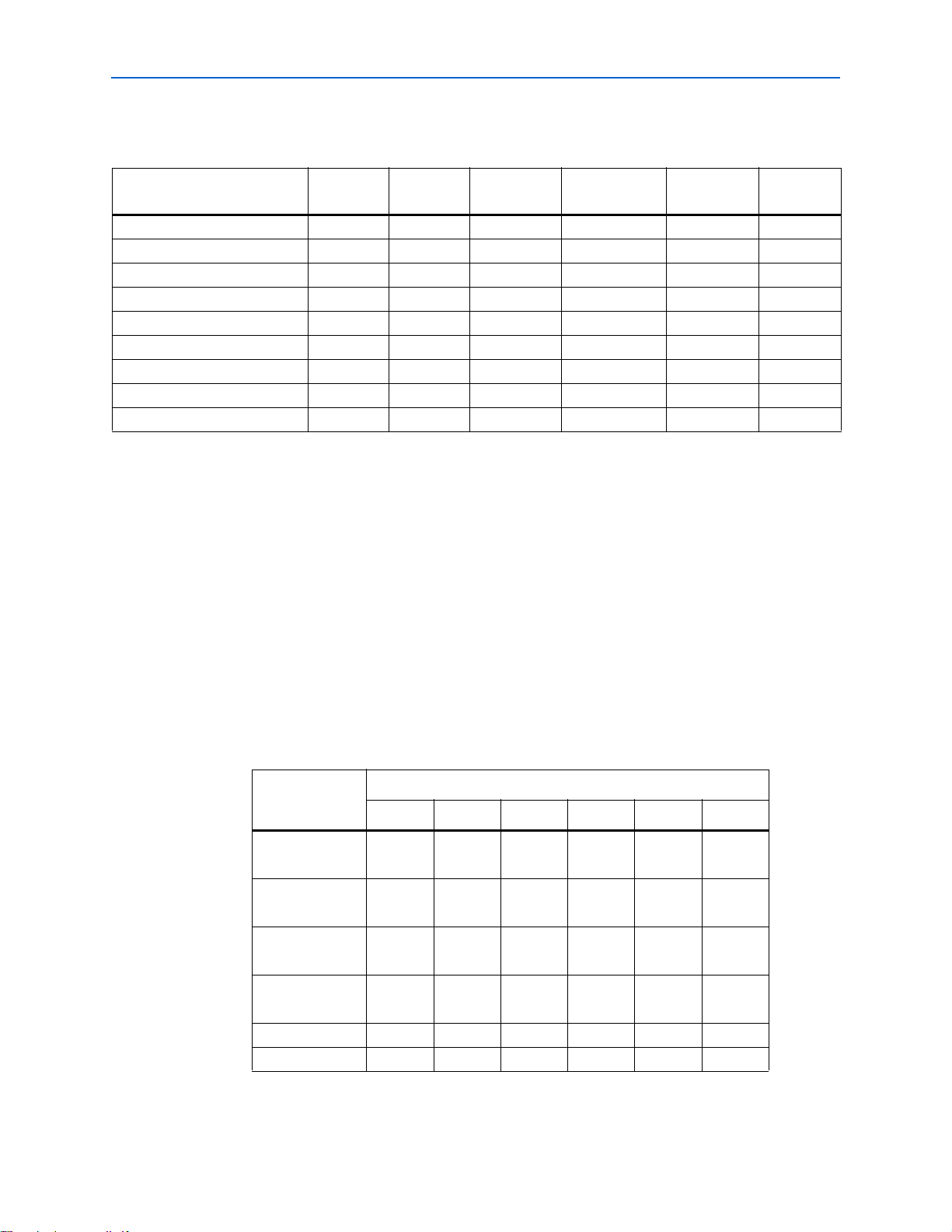
Tab le 1 –1 . MAX II Family Features
Feature
EPM240
EPM240G
EPM570
EPM570G
EPM1270
EPM1270G
EPM2210
EPM2210G EPM240Z EPM570Z
LEs 240 570 1,270 2,210 240 570
Typical Equivalent Macrocells 192 440 980 1,700 192 440
Equiv alent Macrocell Range 128 to 240 240 to 570 570 to 1,270 1,270 to 2,210 128 to 240 240 to 570
UFM Size (bits) 8,192 8,192 8,192 8,192 8,192 8,192
Maximum User I/O pins 80 160 212 272 80 160
(ns) (1) 4.7 5.4 6.2 7.0 7.5 9.0
t
PD1
(MHz) (2) 304 304 304 304 152 152
f
CNT
(ns) 1.7 1.2 1.2 1.2 2.3 2.2
t
SU
(ns) 4.3 4.5 4.6 4.6 6.5 6.7
t
CO
Notes to Ta bl e 1– 1:
(1) t
represents a pin-to-pin delay for the worst case I/O placement with a full diagonal path across the device and combinational logic
PD1
implemented in a single LUT and LAB that is adjacent to the output pin.
(2) The maximum frequency is limited by the I/O standard on the clock input pin. The 16-bit counter critical delay will run faster than this number.
f For more information about equivalent macrocells, refer to the MAX II Logic Element to
Macrocell Conversion Methodology white paper.
MAX II and MAX IIG devices are available in three speed grades: –3, –4, and –5, with
–3 being the fastest. Similarly, MAX IIZ devices are available in three speed grades: –6,
–7, and –8, with –6 being the fastest. These speed grades represent the overall relative
performance, not any specific timing parameter. For propagation delay timing
numbers within each speed grade and density, refer to the DC and Switching
Characteristics chapter in the MAX II Device Handbook.
Table 1–2 shows MAX II device speed-grade offerings.
Tab le 1 –2 . MAX II Speed Grades
Speed Grade
Device
EPM240
–3 –4 –5 –6 –7 –8
vvv———
EPM240G
EPM570
vvv———
EPM570G
EPM1270
vvv———
EPM1270G
EPM2210
vvv———
EPM2210G
EPM240Z — — — vvv
EPM570Z ———vvv
MAX II Device Handbook © August 2009 Altera Corporation
Page 19
Chapter 1: Introduction 1–3
Features
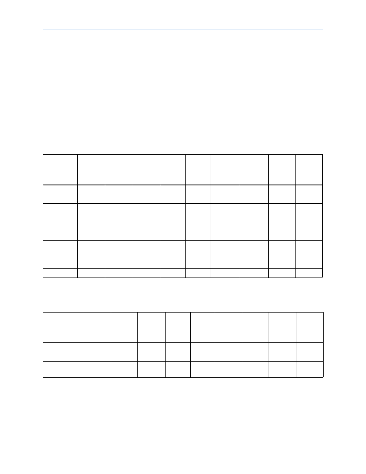
MAX II devices are available in space-saving FineLine BGA, Micro FineLine BGA,
and thin quad flat pack (TQFP) packages (refer to Table 1–3 and Table 1–4). MAX II
devices support vertical migration within the same package (for example, you can
migrate between the EPM570, EPM1270, and EPM2210 devices in the 256-pin
FineLine BGA package). Vertical migration means that you can migrate to devices
whose dedicated pins and JTAG pins are the same and power pins are subsets or
supersets for a given package across device densities. The largest density in any
package has the highest number of power pins; you must lay out for the largest
planned density in a package to provide the necessary power pins for migration. For
I/O pin migration across densities, cross reference the available I/O pins using the
device pin-outs for all planned densities of a given package type to identify which
I/O pins can be migrated. The Quartus® II software can automatically cross-reference
and place all pins for you when given a device migration list.
Tab le 1 –3 . MAX II Packages and User I/O Pins
144-Pin
Micro
FineLine
BGA (1)
144-Pin
Micro
FineLine
BGA
BGA
100-Pin
Micro
FineLine
BGA (1)
100-Pin
Micro
FineLine
BGA
100-Pin
FineLine
BGA
100-Pin
FineLine
BGA
100-Pin
TQFP
100-Pin
TQFP
144-Pin
TQFP
144-Pin
TQFP
68-Pin
Micro
FineLine
Devi ce
EPM240
EPM240G
EPM570
EPM570G
EPM1270
EPM1270G
EPM2210
EPM2210G
EPM240Z 54 80 — — — — — — —
EPM570Z — 76 — — — 116 160 — —
Note to Ta b le 1 –3 :
(1) Packages available in lead-free versions only.
Tab le 1 –4 . MAX II TQFP, FineLine BGA, and Micro Fi neLine BGA Package Sizes
Package
Pitch (mm) 0.5 0.5 1 0.5 0.5 0.5 0.5 1 1
Area (mm2) 25 36 121 256 484 49 121 289 361
Length × width
(mm × mm)
BGA (1)
—808080—— ———
— 76 76 76 116 — 160 160 —
— — — — 116 — 212 212 —
— — ———— —204272
68-Pin
Micro
FineLine
5 × 5 6 × 6 11 × 11 16 × 16 22 × 22 7 × 7 11 × 11 17 × 17 19 × 19
256-Pin
Micro
FineLine
BGA (1)
256-Pin
Micro
FineLine
BGA
256-Pin
FineLine
BGA
256-Pin
FineLine
BGA
324-Pin
FineLine
324-Pin
FineLine
BGA
BGA
© August 2009 Altera Corporation MAX II Device Handbook
Page 20
1–4 Chapter 1: Introduction
Referenced Documents
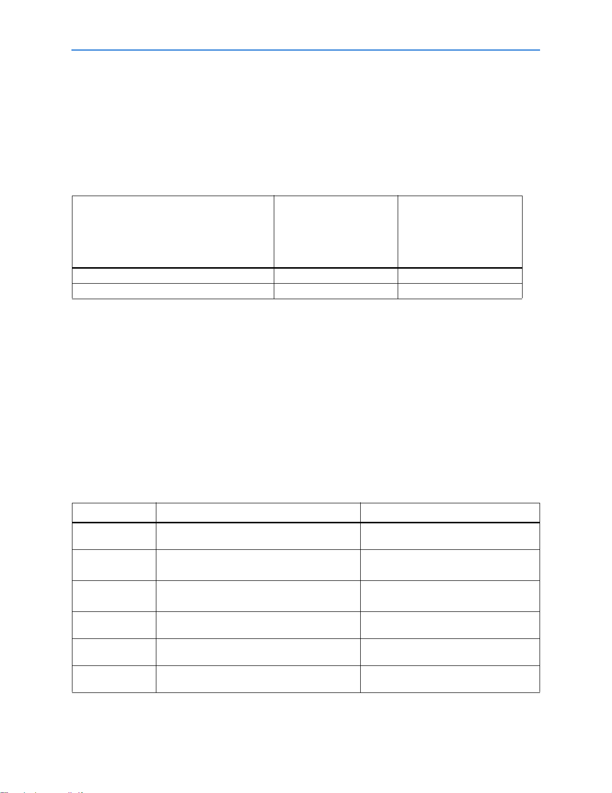
MAX II devices have an internal linear voltage regulator which supports external
supply voltages of 3.3 V or 2.5 V, regulating the supply down to the internal operating
voltage of 1.8 V. MAX IIG and MAX IIZ devices only accept 1.8 V as the external
supply voltage. MAX IIZ devices are pin-compatible with MAX IIG devices in the
100-pin Micro FineLine BGA and 256-pin Micro FineLine BGA packages. Except for
external supply voltage requirements, MAX II and MAX II G devices have identical
pin-outs and timing specifications. Ta b le 1 –5 shows the external supply voltages
supported by the MAX II family.
Tab le 1 –5 . MAX II External Supply Voltages
EPM240G
EPM570G
EPM240
EPM570
EPM1270
Devices
MultiVolt core external supply voltage (V
MultiVolt I/O interface voltage levels (V
Notes to Ta bl e 1– 5:
(1) MAX IIG and MAX IIZ devices only accept 1.8 V on their VCCINT pins. The 1.8-V V
(2) MAX II devices operate internally at 1.8 V.
) (2) 3.3 V, 2.5 V 1.8 V
CCINT
) 1.5 V, 1.8 V, 2.5 V, 3.3 V 1.5 V, 1.8 V, 2.5 V, 3.3 V
CCIO
EPM2210
external supply powers the device core directly.
CCI NT
EPM1270G
EPM2210G
EPM240Z
EPM570Z (1)
Referenced Documents
This chapt er references the following documents:
■ DC and Switching Characteristics chapter in the MAX II Device Handbook
■ MAX II Logic Element to Macrocell Conversion Methodology white paper
Document Revision History
Table 1–6 shows the revision history for this chapter.
Tab le 1 –6 . Document Revision History
Date and Revision Changes Made Summary of Changes
August 2009,
version 1.9
October 2008,
version 1.8
December 2007,
versi on1.7
December 2006,
version 1.6
August 2006,
version 1.5
July 2006,
version 1.4
■ Updated Ta bl e 1– 2. Added information for speed grade –8
■ Updated “Introduction” section.
■ Updated new Document Format.
■ Updated Table 1–1 through Table 1–5.
■ Added “Referenced Documents” section.
■ Added document revision history. —
■ Minor update to features list. —
■ Minor updates to tables. —
Updated document with MAX IIZ information.
—
MAX II Device Handbook © August 2009 Altera Corporation
Page 21

Chapter 1: Introduction 1–5
Document Revision History
Tab le 1 –6 . Document Revision History
Date and Revision Changes Made Summary of Changes
June 2005,
■ Updated timing numbers in Table 1-1. —
version 1.3
December 2004,
■ Updated timing numbers in Table 1-1. —
version 1.2
June 2004,
■ Updated timing numbers in Table 1-1. —
version 1.1
© August 2009 Altera Corporation MAX II Device Handbook
Page 22

1–6 Chapter 1: Introduction
Document Revision History
MAX II Device Handbook © August 2009 Altera Corporation
Page 23

MII51002-2.2
Introduction
2. MAX II Architecture
This chapter describes the architecture of the MAX II device and contains the
following sections:
■ “Functional Description” on page 2–1
■ “Logic Array Blocks” on page 2–4
■ “Logic Elements” on page 2–6
■ “MultiTrack Interconnect” on page 2–12
■ “Global Signals” on page 2–16
■ “User Flash Memory Block” on page 2–18
■ “MultiVolt Core” on page 2–22
■ “I/O Structure” on page 2–23
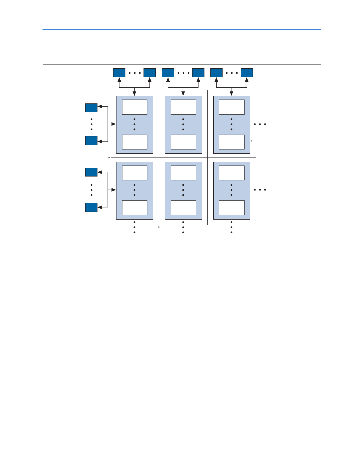
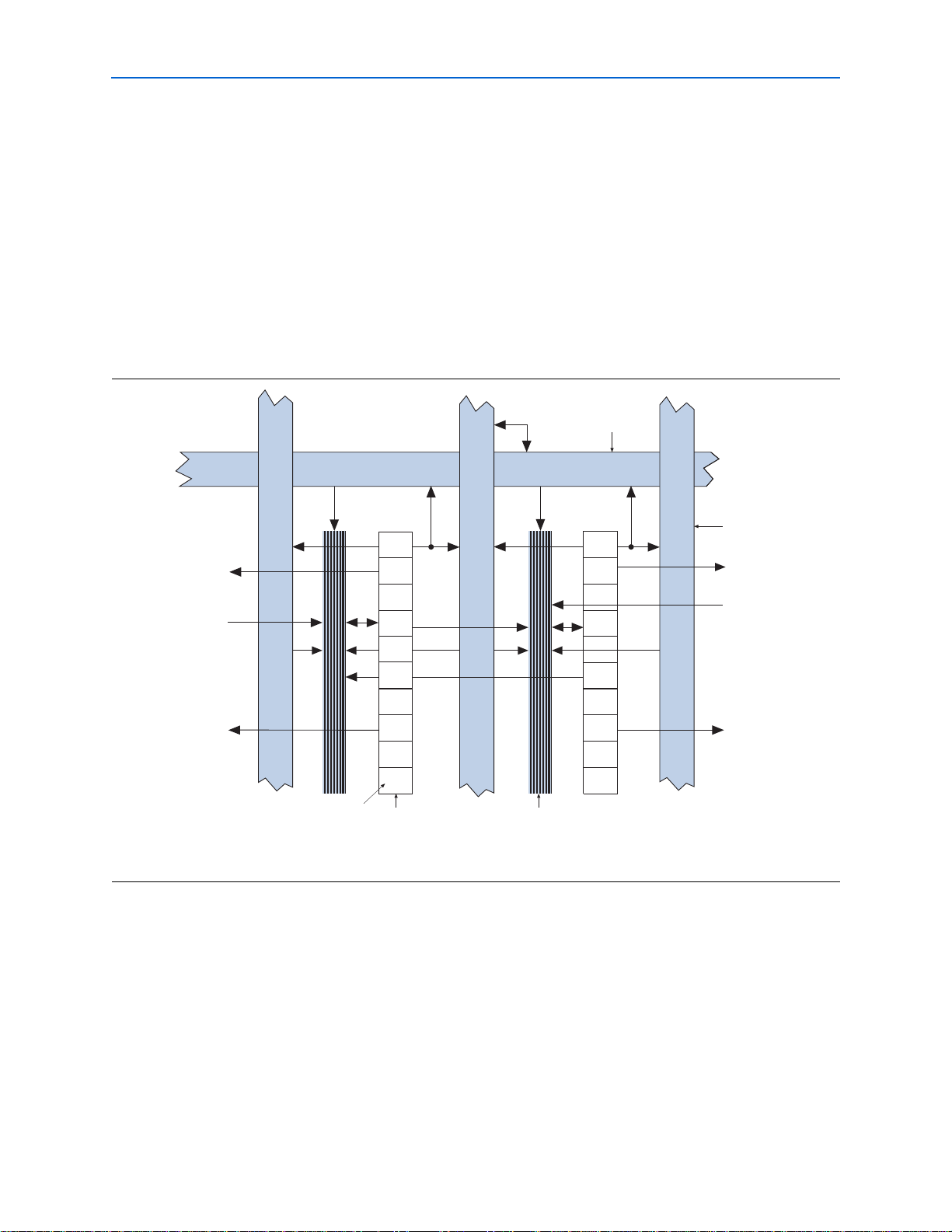
Functional Description
MAX® II devices contain a two-dimensional row- and column-based architecture to
implement custom logic. Row and column interconnects provide signal interconnects
between the logic array blocks (LABs).
The logic array consists of LABs, with 10 logic elements (LEs) in each LAB. An LE is a
small unit of logic providing efficient implementation of user logic functions. LABs
are grouped into rows and columns across the device. The MultiTrack interconnect
provides fast granular timing delays between LABs. The fast routing between LEs
provides minimum timing delay for added levels of logic versus globally routed
interconnect structures.
The MAX II device I/O pins are fed by I/O elements (IOE) located at the ends of LAB
rows and columns around the periphery of the device. Each IOE contains a
bidirectional I/O buffer with several advanced features. I/O pins support Schmitt
trigger inputs and various single-ended standards, such as 66-MHz, 32-bit PCI, and
LVTTL.
MAX II devices provide a global clock network. The global clock network consists of
four global clock lines that drive throughout the entire device, providing clocks for all
resources within the device. The global clock lines can also be used for control signals
such as clear, preset, or output enable.
© October 2008 Altera Corporation MAX II Device Handbook
Page 24
2–2 Chapter 2: MAX II Architecture
Logic Array
BLock (LAB)
MultiTrack
Interconnect
MultiTrack
Interconnect
Logic
Element
Logic
Element
IOE
IOE
IOE IOE
Logic
Element
Logic
Element
IOE
IOE
Logic
Element
Logic
Element
IOE IOE
Logic
Element
Logic
Element
Logic
Element
Logic
Element
IOE IOE
Logic
Element
Logic
Element
Functional Description
Figure 2–1 shows a functional block diagram of the MAX II device.
Figur e 2–1. MAX II Device Block Diagram
Each MAX II device contains a flash memory block within its floorplan. On the
EPM240 device, this block is located on the left side of the device. On the EPM570,
EPM1270, and EPM2210 devices, the flash memory block is located on the bottom-left
area of the device. The majority of this flash memory storage is partitioned as the
dedicated configuration flash memory (CFM) block. The CFM block provides the nonvolatile storage for all of the SRAM configuration information. The CFM
automatically downloads and configures the logic and I/O at power-up, providing
instant-on operation.
f For more information about configuration upon power-up, refer to the Hot Socketing
and Power-On Reset in MAX II Devices chapter in the MAX II Device Handbook.
A portion of the flash memory within the MAX II device is partitioned into a small
block for user data. This user flash memory (UFM) block provides 8,192 bits of
general-purpose user storage. The UFM provides programmable port connections to
the logic array for reading and writing. There are three LAB rows adjacent to this
block, with column numbers varying by device.
Table 2–1 shows the number of LAB rows and columns in each device, as well as the
number of LAB rows and columns adjacent to the flash memory area in the EPM570,
EPM1270, and EPM2210 devices. The long LAB rows are full LAB rows that extend
from one side of row I/O blocks to the other. The short LAB rows are adjacent to the
UFM block; their length is shown as width in LAB columns.
MAX II Device Handbook © October 2008 Altera Corporation
Page 25
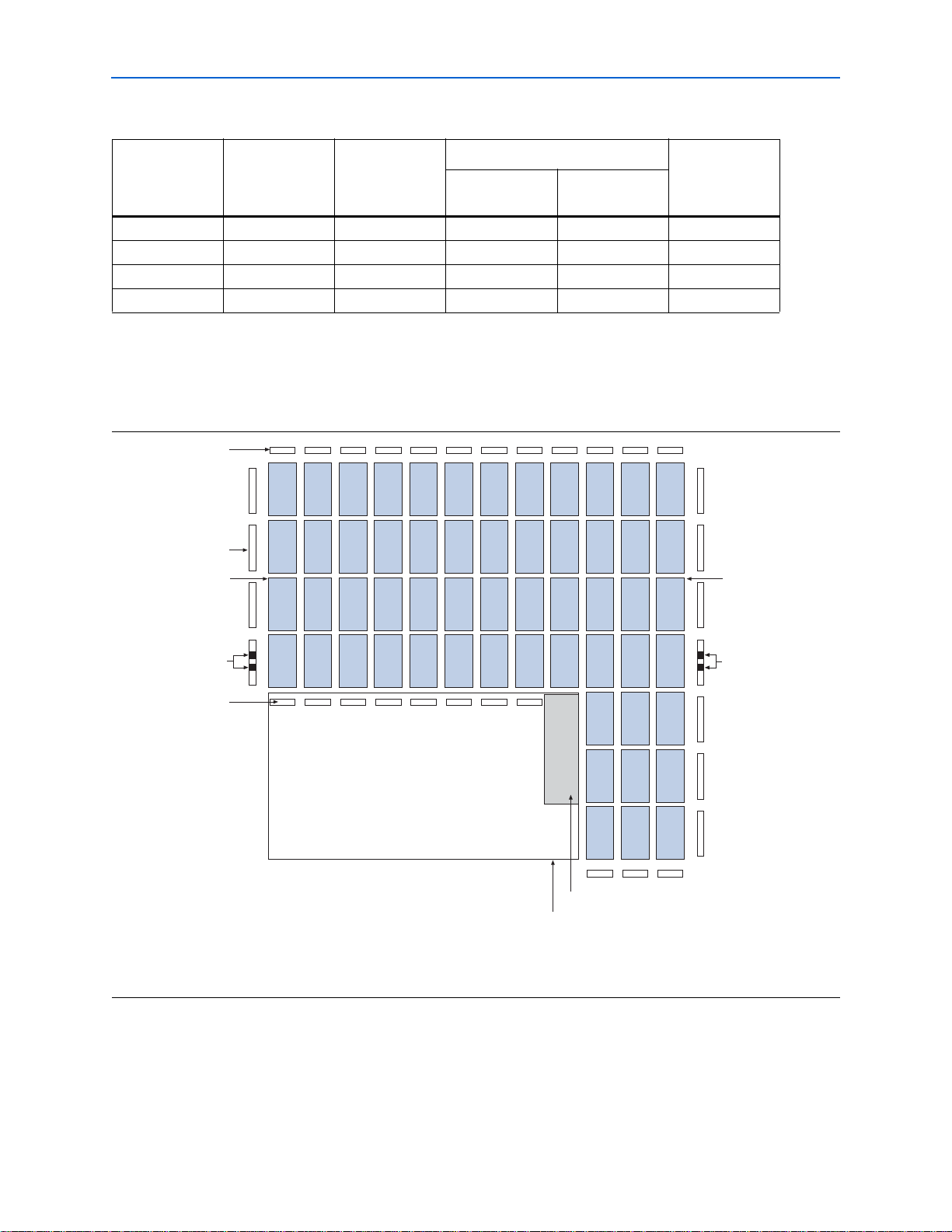
Chapter 2: MAX II Architecture 2–3
y
Functional Description
Tab le 2 –1 . MAX II Device Resources
LAB Rows
Short LAB Rows
Devic es UFM Blocks LAB Columns
(Width) (1)
Total LA BsLong LAB Rows
EPM240 164—24
EPM570 11243 (3)57
EPM1270 1 16 7 3 (5) 127
EPM2210 1 20 10 3 (7) 221
Note to Ta b le 2 –1 :
(1) The width is the number of LAB columns in length.
Figure 2–2 shows a floorplan of a MAX II device.
Figur e 2–2. MAX II Device Floorplan (Note 1)
I/O Blocks
I/O Blocks
Logic Array
Blocks
2 GCLK
Inputs
I/O Blocks
UFM Block
CFM Block
Logic Arra
Blocks
2 GCLK
Inputs
Note to Fi gure 2–2:
(1) The device shown is an EPM570 device. EPM1270 and EPM2210 devices have a similar floorplan with more LABs. For EPM240 devices, the CFM
and UFM blocks are located on the left side of the device.
© October 2008 Altera Corporation MAX II Device Handbook
Page 26
2–4 Chapter 2: MAX II Architecture
Logic Array Blocks
Logic Array Blocks
Each LAB consists of 10 LEs, LE carry chains, LAB control signals, a local interconnect,
a look-up table (LUT) chain, and register chain connection lines. There are 26 possible
unique inputs into an LAB, with an additional 10 local feedback input lines fed by LE
outputs in the same LAB. The local interconnect transfers signals between LEs in the
same LAB. LUT chain connections transfer the output of one LE’s LUT to the adjacent
LE for fast sequential LUT connections within the same LAB. Register chain
connections transfer the output of one LE’s register to the adjacent LE’s register
within an LAB. The Quartus® II software places associated logic within an LAB or
adjacent LABs, allowing the use of local, LUT chain, and register chain connections
for performance and area efficiency. Figure 2–3 shows the MAX II LAB.
Figur e 2–3. MAX II LAB Str ucture
Row Interconnect
Fast I/O connection
to IOE (1)
DirectLink
interconnect from
adjacent LAB
or IOE
DirectLink
interconnect to
adjacent LAB
or IOE
Note to Fi gure 2–3:
(1) Only from LABs adjacent to IOEs.
LAB Interconnects
The LAB local interconnect can drive LEs within the same LAB. The LAB local
interconnect is driven by column and row interconnects and LE outputs within the
same LAB. Neighboring LABs, from the left and right, can also drive an LAB’s local
interconnect through the DirectLink connection. The DirectLink connection feature
minimizes the use of row and column interconnects, providing higher performance
and flexibility. Each LE can drive 30 other LEs through fast local and DirectLink
interconnects. Figure 2–4 shows the DirectLink connection.
Logic Element
LE0
LE1
LE2
LE3
LE4
LE5
LE6
LE7
LE8
LE9
Column Interconnect
Fast I/O connection
to IOE (1)
DirectLink
interconnect from
adjacent LAB
or IOE
DirectLink
interconnect to
adjacent LAB
or IOE
Local InterconnectLAB
MAX II Device Handbook © October 2008 Altera Corporation
Page 27
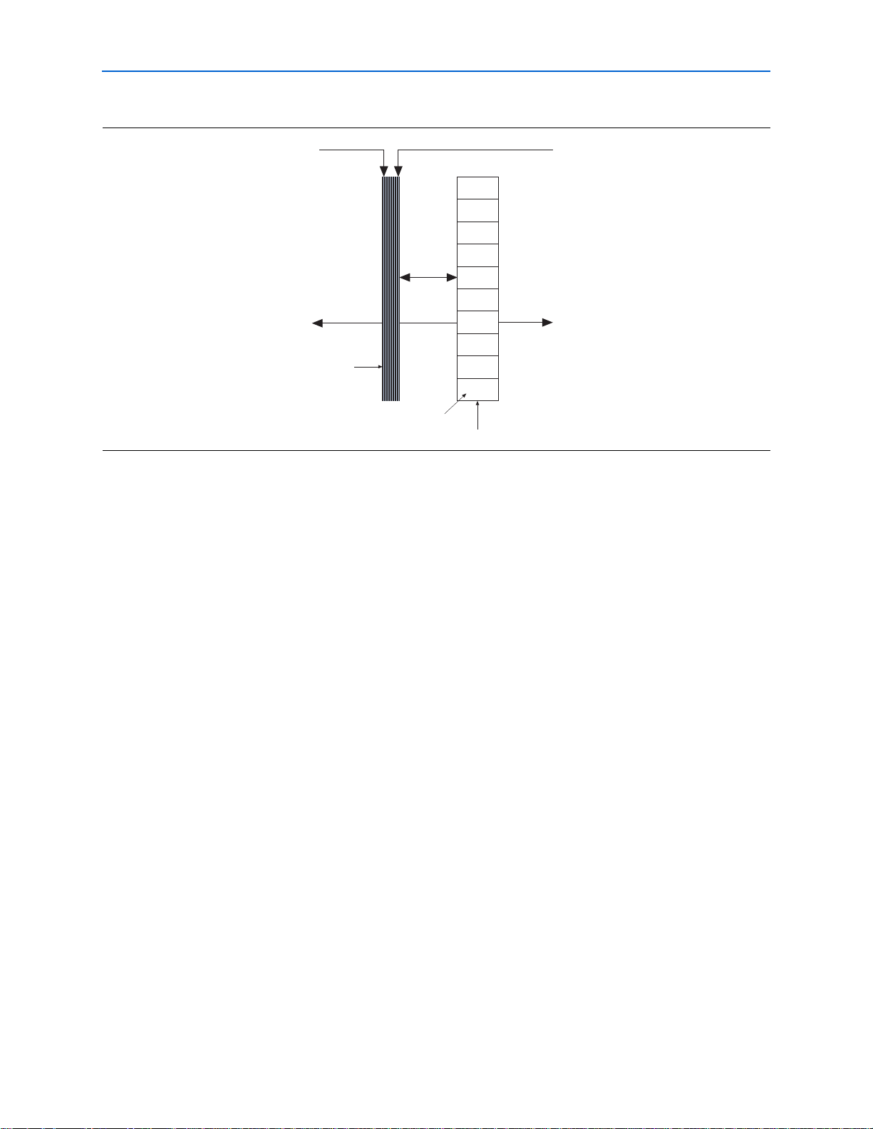
Chapter 2: MAX II Architecture 2–5
Logic Array Blocks
Figur e 2–4. DirectLink Connection
DirectLink interconnect from
left LAB or IOE output
LAB Control Signals
Each LAB contains dedicated logic for driving control signals to its LEs. The control
signals include two clocks, two clock enables, two asynchronous clears, a
synchronous clear, an asynchronous preset/load, a synchronous load, and
add/subtract control signals, providing a maximum of 10 control signals at a time.
Although synchronous load and clear signals are generally used when implementing
counters, they can also be used with other functions.
DirectLink
interconnect
to left
Local
Interconnect
Logic Element
LE0
LE1
LE2
LE3
LE4
LE5
LE6
LE7
LE8
LE9
LAB
DirectLink interconnect from
right LAB or IOE output
DirectLink
interconnect
to right
Each LAB can use two clocks and two clock enable signals. Each LAB’s clock and
clock enable signals are linked. For example, any LE in a particular LAB using the
labclk1 signal also uses labclkena1. If the LAB uses both the rising and falling
edges of a clock, it also uses both LAB-wide clock signals. Deasserting the clock
enable signal turns off the LAB-wide clock.
Each LAB can use two asynchronous clear signals and an asynchronous load/preset
signal. By default, the Quartus II software uses a NOT gate push-back technique to
achieve preset. If you disable the NOT gate push-back option or assign a given register
to power-up high using the Quartus II software, the preset is then achieved using the
asynchronous load signal with asynchronous load data input tied high.
With the LAB-wide addnsub control signal, a single LE can implement a one-bit adder
and subtractor. This saves LE resources and improves performance for logic functions
such as correlators and signed multipliers that alternate between addition and
subtraction depending on data.
The LAB column clocks [3..0], driven by the global clock network, and LAB local
interconnect generate the LAB-wide control signals. The MultiTrack interconnect
structure drives the LAB local interconnect for non-global control signal generation.
The MultiTrack interconnect’s inherent low skew allows clock and control signal
distribution in addition to data. Figure 2–5 shows the LAB control signal generation
circuit.
© October 2008 Altera Corporation MAX II Device Handbook
Page 28
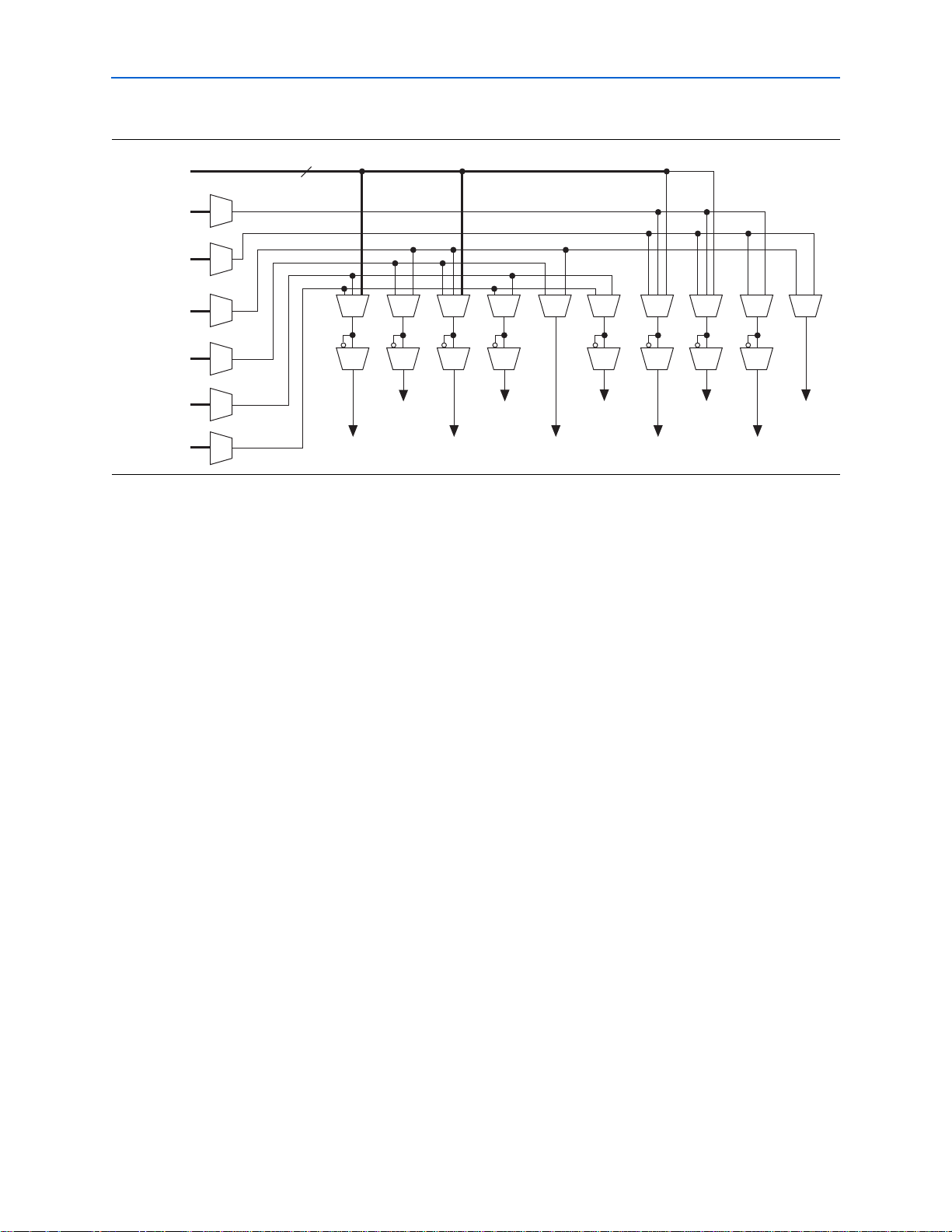
2–6 Chapter 2: MAX II Architecture
labclkena1
labclk2labclk1
labclkena2
asyncload
or labpre
syncload
Dedicated
LAB Column
Clocks
Local
Interconnect
Local
Interconnect
Local
Interconnect
Local
Interconnect
Local
Interconnect
Local
Interconnect
labclr1
labclr2
synclr
addnsub
4
Logic Elements
Figur e 2–5. LAB-Wide Control Signals
Logic Elements
The smallest unit of logic in the MAX II architecture, the LE, is compact and provides
advanced features with efficient logic utilization. Each LE contains a four-input LUT,
which is a function generator that can implement any function of four variables. In
addition, each LE contains a programmable register and carry chain with carry-select
capability. A single LE also supports dynamic single-bit addition or subtraction mode
selectable by an LAB-wide control signal. Each LE drives all types of interconnects:
local, row, column, LUT chain, register chain, and DirectLink interconnects. See
Figure 2–6.
MAX II Device Handbook © October 2008 Altera Corporation
Page 29
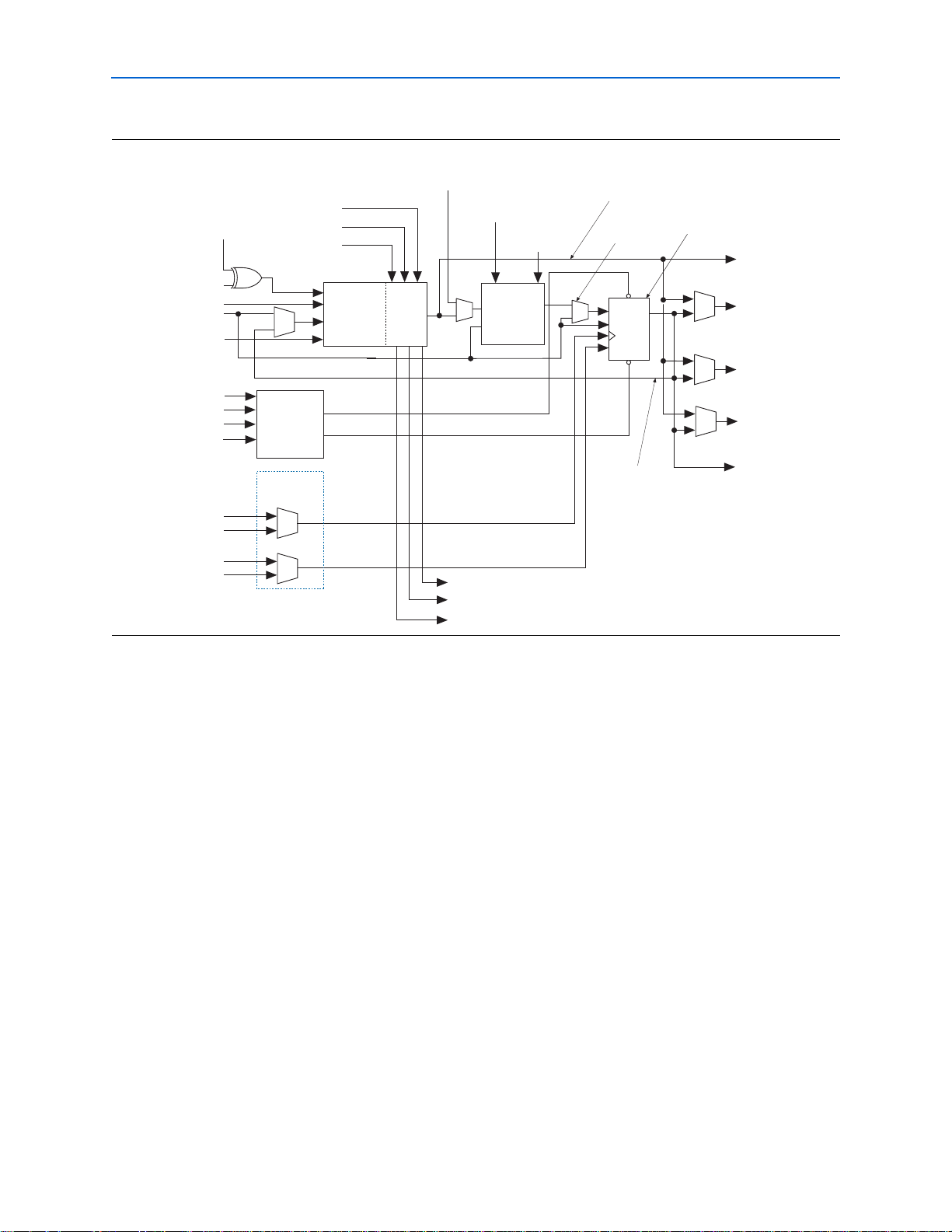
Chapter 2: MAX II Architecture 2–7
Logic Elements
Figur e 2–6. MAX II LE
Register chain
routing from
addnsub
data1
data2
data3
data4
labclr1
labclr2
labpre/aload
Chip-Wide
Reset (DEV_CLRn)
labclk1
labclk2
LAB Carry-In
Carry-In1
Carry-In0
Asynchronous
Clear/Preset/
Load Logic
Clock and
Clock Enable
Select
Look-Up
Table
(LUT)
Carry
Chain
previous LE
LAB-wide
Synchronous
Load
Synchronous
Synchronous
Load and
Clear Logic
LAB-wide
Clear
Register Bypass
Packed
Register Select
PRN/ALD
D
ADATA
ENA
CLRN
Register
Feedback
Programmable
Register
LUT chain
routing to next LE
Row, column,
Q
and DirectLink
routing
Row, column,
and DirectLink
routing
Local routing
Register chain
output
labclkena1
labclkena2
Carry-Out0
Carry-Out1
LAB Carry-Out
Each LE’s programmable register can be configured for D, T, JK, or SR operation. Each
register has data, true asynchronous load data, clock, clock enable, clear, and
asynchronous load/preset inputs. Global signals, general-purpose I/O pins, or any
LE can drive the register’s clock and clear control signals. Either general-purpose I/O
pins or LEs can drive the clock enable, preset, asynchronous load, and asynchronous
data. The asynchronous load data input comes from the data3 input of the LE. For
combinational functions, the LUT output bypasses the register and drives directly to
the LE outputs.
Each LE has three outputs that drive the local, row, and column routing resources. The
LUT or register output can drive these three outputs independently. Two LE outputs
drive column or row and DirectLink routing connections and one drives local
interconnect resources. This allows the LUT to drive one output while the register
drives another output. This register packing feature improves device utilization
because the device can use the register and the LUT for unrelated functions. Another
special packing mode allows the register output to feed back into the LUT of the same
LE so that the register is packed with its own fan-out LUT. This provides another
mechanism for improved fitting. The LE can also drive out registered and
unregistered versions of the LUT output.
© October 2008 Altera Corporation MAX II Device Handbook
Page 30

2–8 Chapter 2: MAX II Architecture
Logic Elements
LUT Chain and Register Chain
In addition to the three general routing outputs, the LEs within an LAB have LUT
chain and register chain outputs. LUT chain connections allow LUTs within the same
LAB to cascade together for wide input functions. Register chain outputs allow
registers within the same LAB to cascade together. The register chain output allows an
LAB to use LUTs for a single combinational function and the registers to be used for
an unrelated shift register implementation. These resources speed up connections
between LABs while saving local interconnect resources. Refer to “MultiTrack
Interconnect” on page 2–12 for more information about LUT chain and register chain
connections.
addnsub Signal
The LE’s dynamic adder/subtractor feature saves logic resources by using one set of
LEs to implement both an adder and a subtractor. This feature is controlled by the
LAB-wide control signal addnsub. The addnsub signal sets the LAB to perform either
A + B or A – B. The LUT computes addition; subtraction is computed by adding the
two’s complement of the intended subtractor. The LAB-wide signal converts to two’s
complement by inverting the B bits within the LAB and setting carry-in to 1, which
adds one to the least significant bit (LSB). The LSB of an adder/subtractor must be
placed in the first LE of the LAB, where the LAB-wide addnsub signal automatically
sets the carry-in to 1. The Quartus II Compiler automatically places and uses the
adder/subtractor feature when using adder/subtractor parameterized functions.
LE Operating Modes
The MAX II LE can operate in one of the following modes:
■ “Normal Mode”
■ “Dynamic Arithmetic Mode”
Each mode uses LE resources differently. In each mode, eight available inputs to the
LE, the four data inputs from the LAB local interconnect, carry-in0 and carry-
in1 from the previous LE, the LAB carry-in from the previous carry-chain LAB, and
the register chain connection are directed to different destinations to implement the
desired logic function. LAB-wide signals provide clock, asynchronous clear,
asynchronous preset/load, synchronous clear, synchronous load, and clock enable
control for the register. These LAB-wide signals are available in all LE modes. The
addnsub control signal is allowed in arithmetic mode.
The Quartus II software, in conjunction with parameterized functions such as library
of parameterized modules (LPM) functions, automatically chooses the appropriate
mode for common functions such as counters, adders, subtractors, and arithmetic
functions.
MAX II Device Handbook © October 2008 Altera Corporation
Page 31

Chapter 2: MAX II Architecture 2–9
data1
4-Input
LUT
data2
data3
cin (from cout
of previous LE)
data4
addnsub (LAB Wide)
clock (LAB Wide)
ena (LAB Wide)
aclr (LAB Wide)
aload
(LAB Wide)
ALD/PRE
CLRN
D
Q
ENA
ADATA
sclear
(LAB Wide)
sload
(LAB Wide)
Register chain
connection
LUT chain
connection
Register
chain output
Row, column, and
DirectLink routing
Row, column, and
DirectLink routing
Local routing
Register Feedback
(1)
Logic Elements
Normal Mode
The normal mode is suitable for general logic applications and combinational
functions. In normal mode, four data inputs from the LAB local interconnect are
inputs to a four-input LUT (see Figure 2–7). The Quartus II Compiler automatically
selects the carry-in or the data3 signal as one of the inputs to the LUT. Each LE can use
LUT chain connections to drive its combinational output directly to the next LE in the
LAB. Asynchronous load data for the register comes from the data3 input of the LE.
LEs in normal mode support packed registers.
Figur e 2–7. LE in Normal Mode
Note to Fi gure 2–7:
(1) This signal is only allowed in normal mode if the LE is at the end of an adder/subtractor chain.
Dynamic Arithmetic Mode
The dynamic arithmetic mode is ideal for implementing adders, counters,
accumulators, wide parity functions, and comparators. An LE in dynamic arithmetic
mode uses four 2-input LUTs configurable as a dynamic adder/subtractor. The first
two 2-input LUTs compute two summations based on a possible carry-in of 1 or 0; the
other two LUTs generate carry outputs for the two chains of the carry-select circuitry.
As shown in Figure 2–8, the LAB carry-in signal selects either the carry-in0 or
carry-in1 chain. The selected chain’s logic level in turn determines which parallel sum
is generated as a combinational or registered output. For example, when
implementing an adder, the sum output is the selection of two possible calculated
sums:
data1 + data2 + carry in0
or
data1 + data2 + carry-in1
© October 2008 Altera Corporation MAX II Device Handbook
Page 32

2–10 Chapter 2: MAX II Architecture
d
d
Logic Elements
The other two LUTs use the data1 and data2 signals to generate two possible carry-out
signals: one for a carry of 1 and the other for a carry of 0. The carry-in0 signal acts
as the carry-select for the carry-out0 output and carry-in1 acts as the carryselect for the carry-out1 output. LEs in arithmetic mode can drive out registered
and unregistered versions of the LUT output.
The dynamic arithmetic mode also offers clock enable, counter enable, synchronous
up/down control, synchronous clear, synchronous load, and dynamic
adder/subtractor options. The LAB local interconnect data inputs generate the
counter enable and synchronous up/down control signals. The synchronous clear
and synchronous load options are LAB-wide signals that affect all registers in the
LAB. The Quartus II software automatically places any registers that are not used by
the counter into other LABs. The addnsub LAB-wide signal controls whether the LE
acts as an adder or subtractor.
Figur e 2–8. LE in Dynamic Arithmetic Mode
LAB Carry-In
Carry-In0
Carry-In1
addnsub
(LAB Wide)
data1
data2
data3
(1)
LUT
LUT
LUT
LUT
sload
(LAB Wide)
Register chain
connection
clock (LAB Wide)
ena (LAB Wide)
aclr (LAB Wide)
Carry-Out1Carry-Out0
sclear
(LAB Wide)
Register Feedback
Note to Fi gure 2–8:
(1) The addnsub signal is tied to the carry input for the first LE of a carry chain only.
aload
(LAB Wide)
ALD/PRE
ADATA
D
ENA
CLRN
Q
Row, column, an
direct link routing
Row, column, an
direct link routing
Local routing
LUT chain
connection
Register
chain output
Carry-Select Chain
The carry-select chain provides a very fast carry-select function between LEs in
dynamic arithmetic mode. The carry-select chain uses the redundant carry calculation
to increase the speed of carry functions. The LE is configured to calculate outputs for a
possible carry-in of 0 and carry-in of 1 in parallel. The carry-in0 and carry-in1
signals from a lower-order bit feed forward into the higher-order bit via the parallel
carry chain and feed into both the LUT and the next portion of the carry chain. Carryselect chains can begin in any LE within an LAB.
MAX II Device Handbook © October 2008 Altera Corporation
Page 33

Chapter 2: MAX II Architecture 2–11
LE3
LE2
LE1
LE0
A1
B1
A2
B2
A3
B3
A4
B4
Sum1
Sum2
Sum3
Sum4
LE9
LE8
LE7
LE6
A7
B7
A8
B8
A9
B9
A10
B10
Sum7
LE5
A6
B6
Sum6
LE4
A5
B5
Sum5
Sum8
Sum9
Sum10
01
01
LAB Carry-In
LAB Carry-Out
LUT
LUT
LUT
LUT
data1
LAB Carry-In
data2
Carry-In0
Carry-In1
Carry-Out0 Carry-Out1
Sum
To top of adjacent LAB
Logic Elements
The speed advantage of the carry-select chain is in the parallel precomputation of
carry chains. Since the LAB carry-in selects the precomputed carry chain, not every LE
is in the critical path. Only the propagation delays between LAB carry-in generation
(LE 5 and LE 10) are now part of the critical path. This feature allows the MAX II
architecture to implement high-speed counters, adders, multipliers, parity functions,
and comparators of arbitrary width.
Figure 2–9 shows the carry-select circuitry in an LAB for a 10-bit full adder. One
portion of the LUT generates the sum of two bits using the input signals and the
appropriate carry-in bit; the sum is routed to the output of the LE. The register can be
bypassed for simple adders or used for accumulator functions. Another portion of the
LUT generates carry-out bits. An LAB-wide carry-in bit selects which chain is used for
the addition of given inputs. The carry-in signal for each chain, carry-in0 or
carry-in1, selects the carry-out to carry forward to the carry-in signal of the nexthigher-order bit. The final carry-out signal is routed to an LE, where it is fed to local,
row, or column interconnects.
Figur e 2–9. Carry-Select Chain
© October 2008 Altera Corporation MAX II Device Handbook
Page 34

2–12 Chapter 2: MAX II Architecture
MultiTrac k Interconnect
The Quartus II software automatically creates carry chain logic during design
processing, or you can create it manually during design entry. Parameterized
functions such as LPM functions automatically take advantage of carry chains for the
appropriate functions. The Quartus II software creates carry chains longer than 10 LEs
by linking adjacent LABs within the same row together automatically. A carry chain
can extend horizontally up to one full LAB row, but does not extend between LAB
rows.
Clear and Preset Logic Control
LAB-wide signals control the logic for the register’s clear and preset signals. The LE
directly supports an asynchronous clear and preset function. The register preset is
achieved through the asynchronous load of a logic high. MAX II devices support
simultaneous preset/asynchronous load and clear signals. An asynchronous clear
signal takes precedence if both signals are asserted simultaneously. Each LAB
supports up to two clears and one preset signal.
In addition to the clear and preset ports, MAX II devices provide a chip-wide reset pin
(DEV_CLRn) that resets all registers in the device. An option set before compilation in
the Quartus II software controls this pin. This chip-wide reset overrides all other
control signals and uses its own dedicated routing resources (that is, it does not use
any of the four global resources). Driving this signal low before or during power-up
prevents user mode from releasing clears within the design. This allows you to control
when clear is released on a device that has just been powered-up. If not set for its chipwide reset function, the DEV_CLRn pin is a regular I/O pin.
By default, all registers in MAX II devices are set to power-up low. However, this
power-up state can be set to high on individual registers during design entry using
the Quartus II software.
MultiTrack Interconnect
In the MAX II architecture, connections between LEs, the UFM, and device I/O pins
are provided by the MultiTrack interconnect structure. The MultiTrack interconnect
consists of continuous, performance-optimized routing lines used for inter- and intradesign block connectivity. The Quartus II Compiler automatically places critical
design paths on faster interconnects to improve design performance.
The MultiTrack interconnect consists of row and column interconnects that span fixed
distances. A routing structure with fixed length resources for all devices allows
predictable and short delays between logic levels instead of large delays associated
with global or long routing lines. Dedicated row interconnects route signals to and
from LABs within the same row. These row resources include:
■ DirectLink interconnects between LABs
■ R4 interconnects traversing four LABs to the right or left
The DirectLink interconnect allows an LAB to drive into the local interconnect of its
left and right neighbors. The DirectLink interconnect provides fast communication
between adjacent LABs and/or blocks without using row interconnect resources.
MAX II Device Handbook © October 2008 Altera Corporation
Page 35

Chapter 2: MAX II Architecture 2–13
MultiTrack Interconnect
The R4 interconnects span four LABs and are used for fast row connections in a fourLAB region. Every LAB has its own set of R4 interconnects to drive either left or right.
Figure 2–10 shows R4 interconnect connections from an LAB. R4 interconnects can
drive and be driven by row IOEs. For LAB interfacing, a primary LAB or horizontal
LAB neighbor can drive a given R4 interconnect. For R4 interconnects that drive to the
right, the primary LAB and right neighbor can drive on to the interconnect. For R4
interconnects that drive to the left, the primary LAB and its left neighbor can drive on
to the interconnect. R4 interconnects can drive other R4 interconnects to extend the
range of LABs they can drive. R4 interconnects can also drive C4 interconnects for
connections from one row to another.
Figur e 2–10. R4 Interconnect Connections
Adjacent LAB can
drive onto another
LAB’s R4 Interconnect
R4 Interconnect
Driving Left
Neighbor
Notes to Figure 2–10:
(1) C4 interconnects can drive R4 interconnects.
(2) This pattern is repeated for every LAB in the LAB row.
LAB
Primary
LAB (2)
C4 Column Interconnects (1)
LAB
Neighbor
R4 Interconnect
Driving Right
The column interconnect operates similarly to the row interconnect. Each column of
LABs is served by a dedicated column interconnect, which vertically routes signals to
and from LABs and row and column IOEs. These column resources include:
■ LUT chain interconnects within an LAB
■ Register chain interconnects within an LAB
■ C4 interconnects traversing a distance of four LABs in an up and down direction
MAX II devices include an enhanced interconnect structure within LABs for routing
LE output to LE input connections faster using LUT chain connections and register
chain connections. The LUT chain connection allows the combinational output of an
LE to directly drive the fast input of the LE right below it, bypassing the local
interconnect. These resources can be used as a high-speed connection for wide fan-in
© October 2008 Altera Corporation MAX II Device Handbook
Page 36

2–14 Chapter 2: MAX II Architecture
LE0
LE1
LE2
LE3
LE4
LE5
LE6
LE7
LE8
LE9
LUT Chain
Routing to
Adjacent LE
Local
Interconnect
Register Chain
Routing to Adjacent
LE's Register Input
Local Interconnect
Routing Among LEs
in the LAB
MultiTrac k Interconnect
functions from LE 1 to LE 10 in the same LAB. The register chain connection allows
the register output of one LE to connect directly to the register input of the next LE in
the LAB for fast shift registers. The Quartus II Compiler automatically takes
advantage of these resources to improve utilization and performance. Figure 2–11
shows the LUT chain and register chain interconnects.
Figur e 2–11. LUT Chain and Register Chain Interconnect s
The C4 interconnects span four LABs up or down from a source LAB. Every LAB has
its own set of C4 interconnects to drive either up or down. Figure 2–12 shows the C4
interconnect connections from an LAB in a column. The C4 interconnects can drive
and be driven by column and row IOEs. For LAB interconnection, a primary LAB or
its vertical LAB neighbor can drive a given C4 interconnect. C4 interconnects can
MAX II Device Handbook © October 2008 Altera Corporation
drive each other to extend their range as well as drive row interconnects for columnto-column connections.
Page 37

Chapter 2: MAX II Architecture 2–15
C4 Interconnect
Drives Local and R4
Interconnects
Up to Four Rows
Adjacent LAB can
drive onto neighboring
LAB's C4 interconnect
C4 Interconnect
Driving Up
C4 Interconnect
Driving Down
LAB
Row
Interconnect
Local
Interconnect
MultiTrack Interconnect
Figur e 2–12. C4 Interconnect Connections (Note 1)
Note to Fi gure 2–12:
(1) Each C4 interconnect can drive either up or down four rows.
© October 2008 Altera Corporation MAX II Device Handbook
Page 38

2–16 Chapter 2: MAX II Architecture
Global Signals
The UFM block communicates with the logic array similar to LAB-to-LAB interfaces.
The UFM block connects to row and column interconnects and has local interconnect
regions driven by row and column interconnects. This block also has DirectLink
interconnects for fast connections to and from a neighboring LAB. For more
information about the UFM interface to the logic array, see “User Flash Memory
Block” on page 2–18.
Table 2–2 shows the MAX II device routing scheme.
Tab le 2 –2 . MAX II Device Routing Sche me
Destination
LUT
Source
LUT Chain — — — — — — v ————
Register Chain — — — — — — v ————
Local
Interconnect
DirectLink
Interconnect
R4 Interconnect — — v — vv—— ———
C4 Interconnect — — v — vv—— ———
LE vvv v vv—— vvv
UFM Block — — vvvv—— ———
Column IOE — — — — — v —— ———
Row I OE — — — vvv—— ———
Note to Ta b le 2 –2 :
(1) These categories are interconnects.
Chai n
Register
Chai n
——— — ——vv vv—
——v — — ——— ———
Local
(1)
DirectLink
(1) R4 (1) C4 (1) LE
UFM
Block
Column
IOE
Row
IOE
Fast I/O
(1)
Global Signals
Each MAX II device has four dual-purpose dedicated clock pins (GCLK[3..0], two
pins on the left side and two pins on the right side) that drive the global clock network
for clocking, as shown in Figure 2–13. These four pins can also be used as generalpurpose I/O if they are not used to drive the global clock network.
The four global clock lines in the global clock network drive throughout the entire
device. The global clock network can provide clocks for all resources within the
device including LEs, LAB local interconnect, IOEs, and the UFM block. The global
clock lines can also be used for global control signals, such as clock enables,
synchronous or asynchronous clears, presets, output enables, or protocol control
signals such as TRDY and IRDY for PCI. Internal logic can drive the global clock
network for internally-generated global clocks and control signals. Figure 2–13 shows
the various sources that drive the global clock network.
MAX II Device Handbook © October 2008 Altera Corporation
Page 39

Chapter 2: MAX II Architecture 2–17
Global Signals
Figur e 2–13. Global Clock Generation
GCLK0
GCLK1
GCLK2
GCLK3
Logic Array(1)
4
4
Global Clock
Network
Note to F igure 2–13:
(1) Any I/O pin can use a MultiTrack interconnect to route as a logic array-generated global clock signal.
The global clock network drives to individual LAB column signals, LAB column
clocks [3..0], that span an entire LAB column from the top to the bottom of the device.
Unused global clocks or control signals in a LAB column are turned off at the LAB
column clock buffers shown in Figure 2–14. The LAB column clocks [3..0] are
multiplexed down to two LAB clock signals and one LAB clear signal. Other control
signal types route from the global clock network into the LAB local interconnect. See
“LAB Control Signals” on page 2–5 for more information.
© October 2008 Altera Corporation MAX II Device Handbook
Page 40

2–18 Chapter 2: MAX II Architecture
UFM Block (2)
CFM Block
I/O Block Region
I/O Block Region
I/O Block Region
LAB Column
clock[3..0]
LAB Column
clock[3..0]
4 4 4 4 4 4 4 4
User Flash Memory Block
Figur e 2–14. Global Clock Network (Note 1)
Notes to Figure 2–14:
(1) LAB column clocks in I/O block regions provide high fan-out output enable signals.
(2) LAB column clocks drive to the UFM block.
User Flash Memory Block
MAX II devices feature a single UFM block, which can be used like a serial EEPROM
for storing non-volatile information up to 8,192 bits. The UFM block connects to the
logic array through the MultiTrack interconnect, allowing any LE to interface to the
UFM block. Figure 2–15 shows the UFM block and interface signals. The logic array is
used to create customer interface or protocol logic to interface the UFM block data
outside of the device. The UFM block offers the following features:
■ Non-volatile storage up to 16-bit wide and 8,192 total bits
■ Two sectors for partitioned sector erase
■ Built-in internal oscillator that optionally drives logic array
■ Program, erase, and busy signals
MAX II Device Handbook © October 2008 Altera Corporation
Page 41

Chapter 2: MAX II Architecture 2–19
OSC 4
Program
Erase
Control
UFM Sector 1
UFM Sector 0
:
_
Address
Register
PROGRAM
ERASE
OSC_ENA
RTP_BUSY
BUSY
OSC
Data Register
UFM Block
DRDin
DRDout
ARCLK
ARSHFT
ARDin
DRCLK
DRSHFT
16 16
9
User Flash Memory Block
■ Auto-increment addressing
■ Serial interface to logic array with programmable interface
Figur e 2–15. UFM Block and Interface Signals
UFM Storage
Each device stores up to 8,192 bits of data in the UFM block. Table 2–3 shows the data
size, sector, and address sizes for the UFM block.
Tab le 2 –3 . UFM Array Size
© October 2008 Altera Corporation MAX II Device Handbook
Device Total Bits Sectors Address Bits Data Width
EPM240
EPM570
EPM1270
8,192 2
(4,096 bits/sector)
916
EPM2210
There are 512 locations with 9-bit addressing ranging from 000h to 1FFh. Sector 0
address space is 000h to 0FFh and Sector 1 address space is from 100h to 1FFh. The
data width is up to 16 bits of data. The Quartus II software automatically creates logic
to accommodate smaller read or program data widths. Erasure of the UFM involves
individual sector erasing (that is, one erase of sector 0 and one erase of sector 1 is
required to erase the entire UFM block). Since sector erase is required before a
program or write, having two sectors enables a sector size of data to be left untouched
while the other sector is erased and programmed with new data.
Page 42

2–20 Chapter 2: MAX II Architecture
User Flash Memory Block
Internal Oscillator
As shown in Figure 2–15, the dedicated circuitry within the UFM block contains an
oscillator. The dedicated circuitry uses this internally for its read and program
operations. This oscillator's divide by 4 output can drive out of the UFM block as a
logic interface clock source or for general-purpose logic clocking. The typical OSC
output signal frequency ranges from 3.3 to 5.5 MHz, and its exact frequency of
operation is not programmable.
Program, Erase, and Busy Signals
The UFM block’s dedicated circuitry automatically generates the necessary internal
program and erase algorithm once the PROGRAM or ERASE input signals have been
asserted. The PROGRAM or ERASE signal must be asserted until the busy signal
deasserts, indicating the UFM internal program or erase operation has completed. The
UFM block also supports JTAG as the interface for programming and/or reading.
f For more information about programming and erasing the UFM block, refer to the
Using User Flash Memory in MAX II Devices chapter in the MAX II Device Handbook.
Auto-Increment Addressing
The UFM block supports standard read or stream read operations. The stream read is
supported with an auto-increment address feature. Deasserting the ARSHIFT signal
while clocking the ARCLK signal increments the address register value to read
consecutive locations from the UFM array.
Serial Interface
The UFM block supports a serial interface with serial address and data signals. The
internal shift registers within the UFM block for address and data are 9 bits and 16 bits
wide, respectively. The Quartus II software automatically generates interface logic in
LEs for a parallel address and data interface to the UFM block. Other standard
protocol interfaces such as SPI are also automatically generated in LE logic by the
Quartus II software.
f For more information about the UFM interface signals and the Quartus II LE-based
alternate interfaces, refer to the Using User Flash Memory in MAX II Devices chapter in
the MAX II Device Handbook.
UFM Block to Logic Array Interface
The UFM block is a small partition of the flash memory that contains the CFM block,
as shown in Figure 2–1 and Figure 2–2. The UFM block for the EPM240 device is
located on the left side of the device adjacent to the left most LAB column. The UFM
block for the EPM570, EPM1270, and EPM2210 devices is located at the bottom left of
the device. The UFM input and output signals interface to all types of interconnects
(R4 interconnect, C4 interconnect, and DirectLink interconnect to/from adjacent LAB
rows). The UFM signals can also be driven from global clocks, GCLK[3..0]. The
interface region for the EPM240 device is shown in Figure 2–16. The interface regions
for EPM570, EPM1270, and EPM2210 devices are shown in Figure 2–17.
MAX II Device Handbook © October 2008 Altera Corporation
Page 43

Chapter 2: MAX II Architecture 2–21
User Flash Memory Block
Figur e 2–16. EPM240 UFM Block LAB Row Interface (Note 1)
CFM Block
UFM Block
LAB
PROGRAM
ERASE
OSC_ENA
RTP_BUSY
DRDin
DRCLK
DRSHFT
ARin
ARCLK
ARSHFT
DRDout
OSC
BUSY
LAB
LAB
Note to Fi gure 2–16:
(1) The UFM block inputs and outputs can drive to/from all types of interconnects, not only DirectLink interconnects from adjacent row LABs.
© October 2008 Altera Corporation MAX II Device Handbook
Page 44

2–22 Chapter 2: MAX II Architecture
RTP_BUSY
BUSY
OSC
DRDout
DRDin
PROGRAM
ERASE
OSC_ENA
ARCLK
ARSHFT
DRDCLK
DRDSHFT
ARDin
UFM Block
CFM Block
LAB
LAB
LAB
MAX II Device
3.3-V or 2.5-V on
VCCINT Pins
Voltage
Regulator
1.8-V Core
Voltage
MAX IIG or MAX IIZ Device
1.8-V on
VCCINT Pins
1.8-V Core
Voltage
MultiVolt Core
Figur e 2–17. EPM570, EPM1270, and EPM2210 UFM Block LAB Row Interface
MultiVolt Core
The MAX II architecture supports the MultiVolt core feature, which allows MAX II
devices to support multiple VCC levels on the V
regulator provides the necessary 1.8-V internal voltage supply to the device. The
voltage regulator supports 3.3-V or 2.5-V supplies on its inputs to supply the 1.8-V
internal voltage to the device, as shown in Figure 2–18. The voltage regulator is not
guaranteed for voltages that are between the maximum recommended 2.5-V
operating voltage and the minimum recommended 3.3-V operating voltage.
Figur e 2–18. MultiVolt Core Feature in MAX II Devices
The MAX IIG and MAX IIZ devices use external 1.8-V supply. The 1.8-V VCC external
supply powers the device core directly.
supply. An internal linear voltage
CCINT
MAX II Device Handbook © October 2008 Altera Corporation
Page 45

Chapter 2: MAX II Architecture 2–23
I/O Structure
I/O Structure
IOEs support many features, including:
■ LVTTL and LVCMOS I/O standards
■ 3.3-V, 32-bit, 66-MHz PCI compliance
■ Joint Test Action Group (JTAG) boundary-scan test (BST) support
■ Programmable drive strength control
■ Weak pull-up resistors during power-up and in system programming
■ Slew-rate control
■ Tri-state buffers with individual output enable control
■ Bus-hold circuitry
■ Programmable pull-up resistors in user mode
■ Unique output enable per pin
■ Open-d rain outputs
■ Schmitt trigger inputs
■ Fast I/O connection
■ Programmable input delay
MAX II device IOEs contain a bidirectional I/O buffer. Figure 2–19 shows the MAX II
IOE structure. Registers from adjacent LABs can drive to or be driven from the IOE’s
bidirectional I/O buffers. The Quartus II software automatically attempts to place
registers in the adjacent LAB with fast I/O connection to achieve the fastest possible
clock-to-output and registered output enable timing. For input registers, the
Quartus II software automatically routes the register to guarantee zero hold time.
You can set timing assignments in the Quartus II software to achieve desired I/O
timing.
Fast I/O Connection
A dedicated fast I/O connection from the adjacent LAB to the IOEs within an I/O
block provides faster output delays for clock-to-output and tPD propagation delays.
This connection exists for data output signals, not output enable signals or input
signals. Figure 2–20, Figure 2–21, and Figure 2–22 illustrate the fast I/O connection.
© October 2008 Altera Corporation MAX II Device Handbook
Page 46

2–24 Chapter 2: MAX II Architecture
Data_in
Optional Schmitt
Trigger Input
Drive Strength Control
Open-Drain Output
Slew Control
Fast_out
Data_out OE
Optional
PCI Clamp (1)
Programmable
Pull-Up
V
CCIOVCCIO
I/O Pin
Optional Bus-Hold
Circuit
DEV_OE
Programmable
Input Delay
I/O Structure
Figur e 2–19. MAX II IOE Structure
Note to Fi gure 2–19:
(1) Available in EPM1270 and EPM2210 devices only.
I/O Blocks
The IOEs are located in I/O blocks around the periphery of the MAX II device. There
are up to seven IOEs per row I/O block (5 maximum in the EPM240 device) and up to
four IOEs per column I/O block. Each column or row I/O block interfaces with its
adjacent LAB and MultiTrack interconnect to distribute signals throughout the device.
The row I/O blocks drive row, column, or DirectLink interconnects. The column I/O
blocks drive column interconnects.
MAX II Device Handbook © October 2008 Altera Corporation
Page 47

Chapter 2: MAX II Architecture 2–25
I/O Structure
Figure 2–20 shows how a row I/O block connects to the logic array.
Figur e 2–20. Row I/O Block Connection to the Interconnect (Note 1)
R4 Interconnects
LAB Local
Interconnect
LAB
Direct Link
Interconnect
to Adjacent LAB
C4 Interconnects
data_in[6..0]
Direct Link
Interconnect
from Adjacent LAB
I/O Block Local
Interconnect
LAB Column
clock [3..0]
data_out
[6..0]
7
OE
[6..0]
7
fast_out
[6..0]
7
7
Row
I/O Block
Row I/O Block
Contains up to
Seven IOEs
Note to Fi gure 2–20:
(1) Each of the seven IOEs in the row I/O block can have one data_out or fast_out output, one OE output, and one data_in input.
© October 2008 Altera Corporation MAX II Device Handbook
Page 48

2–26 Chapter 2: MAX II Architecture
I/O Structure
Figure 2–21 shows how a column I/O block connects to the logic array.
Figur e 2–21. Column I/O Block Connection to the Interconnect (Note 1)
Column I/O
Column I/O Block
Block Contains
Up To 4 IOEs
I/O Block
Local Interconnect
LAB Local
Interconnect
data_out
[3..0]
R4 Interconnects
C4 Interconnects
OE
[3..0]
4
LAB LAB LAB
4
fast_out
[3..0]
Fast I/O
Interconnect
Path
LAB Local
Interconnect
4
LAB Column
Clock [3..0]
data_in
[3..0]
4
LAB Local
Interconnect
C4 Interconnects
Note to Fi gure 2–21:
(1) Each of the four IOEs in the column I/O block can have one data_out or fast_out output, one OE output, and one data_in input.
I/O Standards and Banks
MAX II device IOEs support the following I/O standards:
■ 3.3-V LVTTL/LVCMOS
■ 2.5-V LVTTL/LVCMOS
■ 1.8-V LVTTL/LVCMOS
■ 1.5-V LVCMOS
■ 3.3-V PCI
MAX II Device Handbook © October 2008 Altera Corporation
Page 49

Chapter 2: MAX II Architecture 2–27
2
I/O Structure
Table 2–4 describes the I/O standards supported by MAX II devices.
Tab le 2 –4 . MAX II I/O Standards
Output Supply Voltage
I/O Standard Type
(VCCIO) (V)
3.3-V LVTTL/LVCMOS Single-ende d 3.3
2.5-V LVTTL/LVCMOS Single-ende d 2.5
1.8-V LVTTL/LVCMOS Single-ende d 1.8
1.5-V LVCMOS Single-ende d 1.5
3.3-V PCI (1) Single-ended 3.3
Note to Ta b le 2 –4 :
(1) The 3.3-V PCI compliant I/O is supported in Bank 3 of the EPM1270 and EPM2210
devices.
The EPM240 and EPM570 devices support two I/O banks, as shown in Figure 2–22.
Each of these banks support all the LVTTL and LVCMOS standards shown in
Table 2–4. PCI compliant I/O is not supported in these devices and banks.
Figur e 2–22. MAX II I/O Banks for EPM240 and EPM570 (Note 1), (2)
I/O Bank 1
All I/O Banks Support
■ 3.3-V LVTTL/LVCMOS
■ 2.5-V LVTTL/LVCMOS
■ 1.8-V LVTTL/LVCMOS
■ 1.5-V LVCMOS
Notes to Figure 2–22:
(1) Figure 2–22 is a top view of the silicon die.
(2) Figure 2–22 is a graphical representation only. Refer to the pin list and the Quartus II software for exact pin locations.
The EPM1270 and EPM2210 devices support four I/O banks, as shown in Figure 2–23.
Each of these banks support all of the LVTTL and LVCMOS standards shown in
Table 2–4. PCI compliant I/O is supported in Bank 3. Bank 3 supports the PCI
clamping diode on inputs and PCI drive compliance on outputs. You must use Bank 3
for designs requiring PCI compliant I/O pins. The Quartus II software automatically
places I/O pins in this bank if assigned with the PCI I/O standard.
I/O Bank
© October 2008 Altera Corporation MAX II Device Handbook
Page 50

2–28 Chapter 2: MAX II Architecture
s
I/O Structure
Figur e 2–23. MAX II I/O Banks for EPM1270 a nd EPM2210 (Note 1), (2)
I/O Bank 2
Also Support
the 3.3-V PCI
I/O Standard
I/O Bank 3
I/O Bank 1
All I/O Banks Support
■ 3.3-V LVTTL/LVCMOS
■ 2.5-V LVTTL/LVCMOS
■ 1.8-V LVTTL/LVCMOS
■ 1.5-V LVCMOS
I/O Bank 4
Notes to Figure 2–23:
(1) Figure 2–23 is a top view of the silicon die.
(2) Figure 2–23 is a graphical representation only. Refer to the pin list and the Quartus II software for exact pin locations.
Each I/O bank has dedicated V
pins that determine the voltage standard support
CCIO
in that bank. A single device can support 1.5-V, 1.8-V, 2.5-V, and 3.3-V interfaces; each
individual bank can support a different standard. Each I/O bank can support
multiple standards with the same V
V
is 3.3 V, Bank 3 can support LVTTL, LVCMOS, and 3.3-V PCI. V
CCIO
for input and output pins. For example, when
CCIO
the input and output buffers in MAX II devices.
The JTAG pins for MAX II devices are dedicated pins that cannot be used as regular
I/O pins. The pins TMS, TDI, TDO, and TCK support all the I/O standards shown in
Table 2–4 on page 2–27 except for PCI. These pins reside in Bank 1 for all MAX II
devices and their I/O standard support is controlled by the V
setting for Bank 1.
CCIO
PCI Compliance
The MAX II EPM1270 and EPM2210 devices are compliant with PCI applications as
well as all 3.3-V electrical specifications in the PCI Local Bus Specification Revision 2.2.
These devices are also large enough to support PCI intellectual property (IP) cores.
Table 2–5 shows the MAX II device speed grades that meet the PCI timing
specifications.
powers both
CCIO
MAX II Device Handbook © October 2008 Altera Corporation
Page 51

Chapter 2: MAX II Architecture 2–29
I/O Structure
Tab le 2 –5 . MAX II Devices and Speed Grades that Support 3.3-V PCI Electrical Specifications and
Meet PCI Timing
Device 33-MHz PCI 66-MHz PCI
EPM1270 All Speed Grades –3 Speed Grade
EPM2210 All Speed Grades –3 Speed Grade
Schmitt Trigger
The input buffer for each MAX II device I/O pin has an optional Schmitt trigger
setting for the 3.3-V and 2.5-V standards. The Schmitt trigger allows input buffers to
respond to slow input edge rates with a fast output edge rate. Most importantly,
Schmitt triggers provide hysteresis on the input buffer, preventing slow-rising noisy
input signals from ringing or oscillating on the input signal driven into the logic array.
This provides system noise tolerance on MAX II inputs, but adds a small, nominal
input delay.
The JTAG input pins (TMS, TCK, and TDI) have Schmitt trigger buffers that are always
enabled.
1 The TCK input is susceptible to high pulse glitches when the input signal fall time is
greater than 200 ns for all I/O standards.
Output Enable Signals
Each MAX II IOE output buffer supports output enable signals for tri-state control.
The output enable signal can originate from the GCLK[3..0] global signals or from
the MultiTrack interconnect. The MultiTrack interconnect routes output enable signals
and allows for a unique output enable for each output or bidirectional pin.
MAX II devices also provide a chip-wide output enable pin (DEV_OE) to control the
output enable for every output pin in the design. An option set before compilation in
the Quartus II software controls this pin. This chip-wide output enable uses its own
routing resources and does not use any of the four global resources. If this option is
turned on, all outputs on the chip operate normally when DEV_OE is asserted. When
the pin is deasserted, all outputs are tri-stated. If this option is turned off, the DEV_OE
pin is disabled when the device operates in user mode and is available as a user I/O
pin.
Programmable Drive Strength
The output buffer for each MAX II device I/O pin has two levels of programmable
drive strength control for each of the LVTTL and LVCMOS I/O standards.
Programmable drive strength provides system noise reduction control for high
performance I/O designs. Although a separate slew-rate control feature exists, using
the lower drive strength setting provides signal slew-rate control to reduce system
noise and signal overshoot without the large delay adder associated with the
slew-rate control feature. Table 2–6 shows the possible settings for the I/O standards
with drive strength control. The Quartus II software uses the maximum current
strength as the default setting. The PCI I/O standard is always set at 20 mA with no
alternate setting.
© October 2008 Altera Corporation MAX II Device Handbook
Page 52

2–30 Chapter 2: MAX II Architecture
I/O Structure
Tab le 2 –6 . Programmable Drive Strength (Note 1)
I/O Standard IOH/IOL Current Strength Setting (mA)
3.3-V LVTTL 16
8
3.3-V LVCMOS 8
4
2.5-V LVTTL/LVCMOS 14
7
1.8-V LVTTL/LVCMOS 6
3
1.5-V LVCMOS 4
2
Note to Ta b le 2 –6 :
(1) The IOH current strength numbers shown are for a condition of a V
is specified by the I/O standard. The IOL current strength numbers shown are for a condition of a V
maximum, where the VOL maximum is specified by the I/O standard. For 2.5-V LVTTL/LVCMOS, the IOH
condition is V
= 1.7 V and the IOL condition is V
OUT
OUT
= 0.7 V.
= VOH minimum, where the VOH minimum
OUT
OUT
= VOL
Slew-Rate Control
The output buffer for each MAX II device I/O pin has a programmable output slewrate control that can be configured for low noise or high-speed performance. A faster
slew rate provides high-speed transitions for high-performance systems. However,
these fast transitions may introduce noise transients into the system. A slow slew rate
reduces system noise, but adds a nominal output delay to rising and falling edges.
The lower the voltage standard (for example, 1.8-V LVTTL) the larger the output
delay when slow slew is enabled. Each I/O pin has an individual slew-rate control,
allowing the designer to specify the slew rate on a pin-by-pin basis. The slew-rate
control affects both the rising and falling edges.
Open-Drain Output
MAX II devices provide an optional open-drain (equivalent to open-collector) output
for each I/O pin. This open-drain output enables the device to provide system-level
control signals (for example, interrupt and write enable signals) that can be asserted
by any of several devices. This output can also provide an additional wired-OR plane.
Programmable Ground Pins
Each unused I/O pin on MAX II devices can be used as an additional ground pin.
This programmable ground feature does not require the use of the associated LEs in
the device. In the Quartus II software, unused pins can be set as programmable GND
on a global default basis or they can be individually assigned. Unused pins also have
the option of being set as tri-stated input pins.
MAX II Device Handbook © October 2008 Altera Corporation
Page 53

Chapter 2: MAX II Architecture 2–31
I/O Structure
Bus Hold
Each MAX II device I/O pin provides an optional bus-hold feature. The bus-hold
circuitry can hold the signal on an I/O pin at its last-driven state. Since the bus-hold
feature holds the last-driven state of the pin until the next input signal is present, an
external pull-up or pull-down resistor is not necessary to hold a signal level when the
bus is tri-stated.
The bus-hold circuitry also pulls undriven pins away from the input threshold
voltage where noise can cause unintended high-frequency switching. The designer
can select this feature individually for each I/O pin. The bus-hold output will drive
no higher than V
the device cannot use the programmable pull-up option.
The bus-hold circuitry uses a resistor to pull the signal level to the last driven state.
The DC and Switching Characteristics chapter in the MAX II Device Handbook gives the
specific sustaining current for each V
overdrive current used to identify the next-driven input level.
The bus-hold circuitry is only active after the device has fully initialized. The bus-hold
circuit captures the value on the pin present at the moment user mode is entered.
to prevent overdriving signals. If the bus-hold feature is enabled,
CCIO
voltage level driven through this resistor and
CCIO
Programmable Pull-Up Resistor
Each MAX II device I/O pin provides an optional programmable pull-up resistor
during user mode. If the designer enables this feature for an I/O pin, the pull-up
resistor holds the output to the V
1 The programmable pull-up resistor feature should not be used at the same time as the
bus-hold feature on a given I/O pin.
Programmable Input Delay
The MAX II IOE includes a programmable input delay that is activated to ensure zero
hold times. A path where a pin directly drives a register, with minimal routing
between the two, may require the delay to ensure zero hold time. However, a path
where a pin drives a register through long routing or through combinational logic
may not require the delay to achieve a zero hold time. The Quartus II software uses
this delay to ensure zero hold times when needed.
MultiVolt I/O Interface
The MAX II architecture supports the MultiVolt I/O interface feature, which allows
MAX II devices in all packages to interface with systems of different supply voltages.
The devices have one set of VCC pins for internal operation (V
sets for input buffers and I/O output driver buffers (V
of I/O banks available in the devices where each set of VCC pins powers one I/O
bank. The EPM240 and EPM570 devices have two I/O banks respectively while the
EPM1270 and EPM2210 devices have four I/O banks respectively.
level of the output pin’s bank.
CCIO
), depending on the number
CCIO
), and up to four
CCINT
© October 2008 Altera Corporation MAX II Device Handbook
Page 54

2–32 Chapter 2: MAX II Architecture
Referenced Documents
Connect VCCIO pins to either a 1.5-V, 1.8 V, 2.5-V, or 3.3-V power supply, depending
on the output requirements. The output levels are compatible with systems of the
same voltage as the power supply (that is, when VCCIO pins are connected to a 1.5-V
power supply, the output levels are compatible with 1.5-V systems). When VCCIO
pins are connected to a 3.3-V power supply, the output high is 3.3 V and is compatible
with 3.3-V or 5.0-V systems. Table 2–7 summarizes MAX II MultiVolt I/O support.
Tab le 2 –7 . MAX II MultiVolt I/O Support (Note 1)
Input Signal Output Signal
VCCIO (V)
1.5
1.8
2.5
3.3
1.5 V 1.8 V 2.5 V 3.3 V 5.0 V 1.5 V 1.8 V 2.5 V 3.3 V 5.0 V
vvvv— v ————
vvvv— v (2) v ———
——vv— v (3) v (3) v ——
——v (4) vv (5) v (6) v (6) v (6) vv (7)
Notes to Ta bl e 2– 7:
(1) To drive inputs higher than V
device, enable the I/O clamp diode to prevent VI from rising above 4.0 V.
(2) When V
(3) When V
(4) When V
(5) MAX II devices can be 5.0-V tolerant with the use of an external resistor and the internal I/O clamp diode on the EPM1270 and EPM2210
devices.
(6) When V
(7) When V
drain setting with internal I/O clamp diode (available only on EPM1270 and EPM2210 devices) and external resistor is required.
= 1.8 V, a MAX II device can drive a 1.5-V device with 1.8-V tolerant inputs.
CCI O
= 2.5 V, a MAX II device can drive a 1.5-V or 1.8-V device with 2.5-V tolerant inputs.
CCI O
= 3.3 V and a 2.5-V input signal feeds an input pin, the VCCIO supply current will be slightly larger than expected.
CCI O
= 3.3 V, a MAX II device can drive a 1.5-V, 1.8-V, or 2.5-V device with 3.3-V tolerant inputs.
CCI O
= 3.3 V, a MAX II device can drive a device with 5.0-V TTL inputs but not 5.0-V CMOS inputs. In the case of 5.0-V CMOS, open-
CCI O
but less than 4.0 V including the overshoot, disable the I /O clamp diode. However, to drive 5.0-V inputs to the
CCIO
f For information about output pin source and sink current guidelines, refer to the AN
428: MAX II CPLD Design Guidelines.
Referenced Documents
This chapter referenced the following documents:
■ AN 428: MAX II CPLD Design Guidelines
■ DC and Switching Characteristics chapter in the MAX II Device Handbook
■ Hot Socketing and Power-On Reset in MAX II Devices chapter in the MAX II Device
Handbook
■ Using User Flash Memory in MAX II Devices chapter in the MAX II Device Handbook
MAX II Device Handbook © October 2008 Altera Corporation
Page 55

Chapter 2: MAX II Architecture 2–33
Document Revision History
Document Revision History
Table 2–8 shows the revision history for this chapter.
Tab le 2 –8 . Document Revision History
Date and Revision Changes Made Summary of Changes
October 2008,
version 2.2
March 2008,
version 2.1
December 2007,
version 2.0
December 2006,
version 1.7
August 2006,
version 1.6
July 2006,
vervion 1.5
February 2006,
version 1.4
August 2005,
version 1.3
December 2004,
version 1.2
June 2004,
version 1.1
■ Updated Tab le 2–4 and Tabl e 2–6.
■ Updated “I/O Standards and Banks” section.
■ Updated New Document Format.
■ Updated “Schmitt Trigger” sec tion. —
■ Updated “Clear and Preset Logic Control” section.
■ Updated “MultiVolt Core” section.
■ Updated “MultiVolt I/O Interface” section.
■ Updated Table 2–7.
■ Added “Referenced Documents” section.
■ Minor update in “Internal Oscil lator” section. Added document
Updated document with
MAX IIZ information.
—
—
revision history.
■ Updated functional description and I/O structure sections. —
■ Minor content and table updates. —
■ Updated “LAB Control Signals” section.
■ Updated “Clear and Preset Logic Control” section.
■ Updated “Internal Oscillat or” section.
■ Updated Table 2–5.
■ Removed Note 2 from Table 2-7. —
■ Adde d a paragr aph to page 2-15. —
■ Adde d CFM acronym. Corrected Figure 2-19. —
—
© October 2008 Altera Corporation MAX II Device Handbook
Page 56

2–34 Chapter 2: MAX II Architecture
Document Revision History
MAX II Device Handbook © October 2008 Altera Corporation
Page 57

3. JTAG and In-System Programmability
MII51003-1.6
Introduction
This chapter discusses how to use the IEEE Standard 1149.1 Boundary-Scan Test (BST)
circuitry in MAX II devices and includes the following sections:
■ “IEEE Std. 1149.1 (JTAG) Boundary-Scan Support” on page 3–1
■ “In System Programmability” on page 3–4
IEEE Std. 1149.1 (JTAG) Boundary-Scan Support
All MAX® II devices provide Joint Test Action Group (JTAG) boundary-scan test (BST)
circuitry that complies with the IEEE Std. 1149.1-2001 specification. JTAG boundaryscan testing can only be performed at any time after V
been fully powered and a t
use the JTAG port for in-system programming together with either the Quartus®II
software or hardware using Programming Object Files (.pof), JamTM Standard Test
and Programming Language (STAPL) Files (.jam), or Jam Byte-Code Files (.jbc).
amount of time has passed. MAX II devices can also
CONFIG
CCINT
and all V
banks have
CCIO
The JTAG pins support 1.5-V, 1.8-V, 2.5-V, or 3.3-V I/O standards. The supported
voltage level and standard are determined by the V
of the bank where it resides.
CCI O
The dedicated JTAG pins reside in Bank 1 of all MAX II devices.
MAX II devices support the JTAG instructions shown in Table 3–1.
Tab le 3 –1 . MAX I I JTAG Instructi ons (Part 1 of 2)
JTAG Instruction Instruction Code Description
SAMPLE/PRELOAD 00 0000 0101 Allows a snapshot of signals at the device pins to be captured and
examined during normal device operat ion, and permits an initial dat a
pattern to be output at the device pins.
EXTEST (1) 00 0000 1111 Allows the external ci rcuitry and board-level interconnects to be
tested by forcing a test pattern at the output pins and capturing test
results at the input pins.
BYPASS 11 1111 1111 Places the 1-bit bypass register between the TDI and TDO pins,
which allows the BST data to pass synchronously through selected
devices to adja cent devices during normal device operation.
USERCODE 00 0000 0111 Selects the 32-bit USERCODE register and places it between the
TDI and TDO pi ns, allowing the USERCODE to be serially shifted
out of TDO. This register defaults to all 1’s if not specified in the
Quartus II software.
IDCODE 00 0000 0110 Selects the IDCODE register and places it between TDI and TDO,
allowing the IDCODE to be serially shifted out of TDO.
HIGHZ (1) 00 0000 1011 Places the 1-bit bypass register between the TDI and TDO pins,
which allows the boundary scan test dat a to pass synchronously
through selected devic es to adjacent devices during normal de vice
operation, whil e tri-stating all of the I/O pins.
© October 2008 Altera Corporation MAX II Device Handbook
Page 58

3–2 Chapter 3: JTAG and In-System Programmability
IEEE Std. 1149.1 (JTAG) Boundary-Scan Support
Tab le 3 –1 . MAX I I JTAG Instructi ons (Part 2 of 2)
JTAG Instruction Instruction Code Description
CLAMP (1) 00 0000 1010 Places the 1-bit bypass register between the TDI and TDO pins,
which allows the boundary scan test dat a to pass synchronously
through selected devic es to adjacent devices during normal de vice
operation, while holding I/O pins to a state defined by the data in the
boundary-scan register.
USER0 00 0000 1100 This instruction allows you to define the scan chain between TDI
and TDO in the MAX II logic array. This instruction is also used for
custom logic and JTAG interfaces.
USER1 00 0000 1110 This instruction allows you to define the scan chain between TDI
and TDO in the MAX II logic array. This instruction is also used for
custom logic and JTAG interfaces.
IEEE 1532
instructions
Notes to Ta bl e 3– 1:
(1) HIGHZ, CLAMP, and EXTEST instructions do not disable weak pull-up resistors or bus hold features.
(2) These instructions are shown in the 1532 BSDL files, which will be posted on the Altera® website at www.altera.com when they are available.
(2) IEEE 1532 ISC instructi ons used whe n programming a MAX II device
via the JTAG port.
w Unsupported JTAG instructions should not be issued to the MAX II device as this may
put the device into an unknown state, requiring a power cycle to recover device
operation.
The MAX II device instruction register length is 10 bits and the USERCODE register
length is 32 bits. Table 3–2 and Table 3–3 show the boundary-scan register length and
device IDCODE information for MAX II devices.
Tab le 3 –2 . MAX I I Boundar y-Scan Register Length
Device Boundary-Scan Register Length
EPM240 240
EPM570 480
EPM1270 636
EPM2210 816
Tab le 3 –3 . 32-Bit MAX II Device IDCODE (Part 1 of 2)
Bina ry IDCODE ( 32 Bits) (1)
Version
Devi ce
EPM240
(4 Bits) Part Number
0000 0010 0000 1010 0001 000 0110 1110 1 0x020A10DD
EPM240G
EPM570
0000 0010 0000 1010 0010 000 0110 1110 1 0x020A20DD
EPM570G
EPM1270
0000 0010 0000 1010 0011 000 0110 1110 1 0x020A30DD
EPM1270G
EPM2210
0000 0010 0000 1010 0100 000 0110 1110 1 0x020A40DD
EPM2210G
Manufacturer
Identity (11 Bits)
LSB
(1 Bit) (2)
HEX IDCODE
MAX II Device Handbook © October 2008 Altera Corporation
Page 59

Chapter 3: JTAG and In-System Programmability 3–3
IEEE Std. 1149.1 (JTAG) Boundary-Scan Support
Tab le 3 –3 . 32-Bit MAX II Device IDCODE (Part 2 of 2)
Bina ry IDCODE ( 32 Bits) (1)
Version
Devi ce
EPM240Z 0000 0010 0000 1010 0101 000 0110 1110 1 0x020A50DD
EPM570Z 0000 0010 0000 1010 0110 000 0110 1110 1 0x020A60DD
Notes to Ta bl e 3– 2:
(1) The most significant bit (MSB) is on the left.
(2) The IDCODE’s least significant bit (LSB) is always 1.
(4 Bits) Part Number
Manufacturer
Identity (11 Bits)
LSB
(1 Bit) (2)
HEX IDCODE
f For JTAG AC characteristics, refer to the DC and Switching Characteristics chapter in
the MAX II Device Handbook.
f For more information about JTAG BST, refer to the IEEE 1149.1 (JTAG) Boundary-Scan
Testing for MAX II Devices chapter in the MAX II Device Handbook.
JTAG Block
The MAX II JTAG block feature allows you to access the JTAG TAP and state signals
when either the USER0 or USER1 instruction is issued to the JTAG TAP. The USER0
and USER1 instructions bring the JTAG boundary-scan chain (TDI) through the user
logic instead of the MAX II device’s boundary-scan cells. Each USER instruction
allows for one unique user-defined JTAG chain into the logic array.
Parallel Flash Loader
The JTAG block ability to interface JTAG to non-JTAG devices is ideal for generalpurpose flash memory devices (such as Intel- or Fujitsu-based devices) that require
programming during in-circuit test. The flash memory devices can be used for FPGA
configuration or be part of system memory. In many cases, the MAX II device is
already connected to these devices as the configuration control logic between the
FPGA and the flash device. Unlike ISP-capable CPLD devices, bulk flash devices do
not have JTAG TAP pins or connections. For small flash devices, it is common to use
the serial JTAG scan chain of a connected device to program the non-JTAG flash
device. This is slow and inefficient in most cases and impractical for large parallel
flash devices. Using the MAX II device’s JTAG block as a parallel flash loader, with
the Quartus II software, to program and verify flash contents provides a fast and costeffective means of in-circuit programming during test. Figure 3–1 shows MAX II
being used as a parallel flash loader.
© October 2008 Altera Corporation MAX II Device Handbook
Page 60

3–4 Chapter 3: JTAG and In-System Programmability
Parallel
Flash Loader
Configuration
Logic
Flash
Memory Device
MAX II Device
DQ[7..0]
RY/BY
A[20..0]
OE
WE
CE
DQ[7..0]
RY/BY
A[20..0]
OE
WE
CE
TDI
TMS
TCK
TDI_U
TDO_U
TMS_U
TCK_U
SHIFT_U
CLKDR_U
UPDATE_U
RUNIDLE_U
USER1_U
TDO
Altera FPGA
CONF_DONE
nSTATUS
nCE
DCLK
DATA0
nCONFIG
(1), (2)
In System Programmability
Figur e 3–1. MAX II Parallel Flash Loader
Notes to Figure 3–1:
(1) This block is implemented in LEs.
(2) This function is supported in the Quartus II software.
In System Programmability
MAX II devices can be programmed in-system via the industry standard 4-pin IEEE
Std. 1149.1 (JTAG) interface. In-system programmability (ISP) offers quick, efficient
iterations during design development and debugging cycles. The logic, circuitry, and
interconnects in the MAX II architecture are configured with flash-based SRAM
configuration elements. These SRAM elements require configuration data to be
loaded each time the device is powered. The process of loading the SRAM data is
called configuration. The on-chip configuration flash memory (CFM) block stores the
SRAM element’s configuration data. The CFM block stores the design’s configuration
pattern in a reprogrammable flash array. During ISP, the MAX II JTAG and ISP
circuitry programs the design pattern into the CFM block’s non-volatile flash array.
The MAX II JTAG and ISP controller internally generate the high programming
voltages required to program the CFM cells, allowing in-system programming with
any of the recommended operating external voltage supplies (that is, 3.3 V/2.5 V or
1.8 V for the MAX IIG and MAX IIZ devices). ISP can be performed anytime after
V
and all V
CCINT
configuration power-up time. By default, during in-system programming, the I/O
pins are tri-stated and weakly pulled-up to V
system programming clamp and real-time ISP feature allow user control of I/O state
or behavior during ISP.
For more information, refer to “In-System Programming Clamp” on page 3–6 and
“Real-Time ISP” on page 3–7.
These devices also offer an ISP_DONE bit that provides safe operation when insystem programming is interrupted. This ISP_DONE bit, which is the last bit
programmed, prevents all I/O pins from driving until the bit is programmed.
MAX II Device Handbook © October 2008 Altera Corporation
banks have been fully powered and the device has completed the
CCIO
to eliminate board conflicts. The in-
CCIO
Page 61

Chapter 3: JTAG and In-System Programmability 3–5
In System Programmability
IEEE 1532 Support
The JTAG circuitry and ISP instruction set in MAX II devices is compliant to the IEEE
1532-2002 programming specification. This provides industry-standard hardware and
software for in-system programming among multiple vendor programmable logic
devices (PLDs) in a JTAG chain.
The MAX II 1532 BSDL files will be released on the Altera website when available.
Jam Standard Test and Programming Language (STAPL)
The Jam STAPL JEDEC standard, JESD71, can be used to program MAX II devices
with in-circuit testers, PCs, or embedded processors. The Jam byte code is also
supported for MAX II devices. These software programming protocols provide a
compact embedded solution for programming MAX II devices.
f For more information, refer to the Using Jam STAPL for ISP via an Embedded Processor
chapter in the MAX II Device Handbook.
Programming Sequence
During in-system programming, 1532 instructions, addresses, and data are shifted
into the MAX II device through the TDI input pin. Data is shifted out through the TDO
output pin and compared against the expected data. Programming a pattern into the
device requires the following six ISP steps. A stand-alone verification of a
programmed pattern involves only stages 1, 2, 5, and 6. These steps are automatically
executed by third-party programmers, the Quartus II software, or the Jam STAPL and
Jam Byte-Code Players.
1. Enter ISP—The enter ISP stage ensures that the I/O pins transition smoothly from
user mode to ISP mod e.
2. Check ID—Before any program or verify process, the silicon ID is checked. The
time required to read this silicon ID is relatively small compared to the overall
programming time.
3. Sector Erase—Erasing the device in-system involves shifting in the instruction to
erase the device and applying an erase pulse(s). The erase pulse is automatically
generated internally by waiting in the run/test/idle state for the specified erase
pulse time of 500 ms for the CFM block and 500 ms for each sector of the UFM
block.
4. Program—Programming the device in-system involves shifting in the address,
data, and program instruction and generating the program pulse to program the
flash cells. The program pulse is automatically generated internally by waiting in
the run/test/idle state for the specified program pulse time of 75 µs. This process
is repeated for each address in the CFM and UFM blocks.
5. Verify—Verifying a MAX II device in-system involves shifting in addresses,
applying the verify instruction to generate the read pulse, and shifting out the data
for comparison. This process is repeated for each CFM and UFM address.
6. Exit ISP—An exit ISP stage ensures that the I/O pins transition smoothly from ISP
mode to user mode.
© October 2008 Altera Corporation MAX II Device Handbook
Page 62

3–6 Chapter 3: JTAG and In-System Programmability
In System Programmability
Table 3–4 shows the programming times for MAX II devices using in-circuit testers to
execute the algorithm vectors in hardware. Software-based programming tools used
with download cables are slightly slower because of data processing and transfer
limitations.
Tab le 3 –4 . MAX II Device Family Programming Times
EPM240
EPM240G
Description
Erase + Program (1 MHz) 1.72 2.16 2.90 3.92 sec
Erase + Program (10 MHz) 1.65 1.99 2.58 3.40 sec
Verify (1 MHz) 0.09 0.17 0.30 0.49 sec
Verify (10 MHz) 0.01 0.02 0.03 0.05 sec
Complete Program Cycle (1 MHz) 1.81 2.33 3.20 4.41 sec
Complete Program Cycle (10 MHz) 1.66 2.01 2.61 3.45 sec
EPM240Z
EPM570
EPM570G
EPM570Z
EPM1270
EPM1270G
EPM2210
EPM2210G Unit
UFM Programming
The Quartus II software, with the use of POF, Jam, or JBC files, supports
programming of the user flash memory (UFM) block independent of the logic array
design pattern stored in the CFM block. This allows updating or reading UFM
contents through ISP without altering the current logic array design, or vice versa. By
default, these programming files and methods will program the entire flash memory
contents, which includes the CFM block and UFM contents. The stand-alone
embedded Jam STAPL player and Jam Byte-Code Player provides action commands
for programming or reading the entire flash memory (UFM and CFM together) or
each independently.
f For more information, refer to the Using Jam STAPL for ISP via an Embedded Processor
chapter in the MAX II Device Handbook.
In-System Programming Clamp
By default, the IEEE 1532 instruction used for entering ISP automatically tri-states all
I/O pins with weak pull-up resistors for the duration of the ISP sequence. However,
some systems may require certain pins on MAX II devices to maintain a specific DC
logic level during an in-field update. For these systems, an optional in-system
programming clamp instruction exists in MAX II circuitry to control I/O behavior
during the ISP sequence. The in-system programming clamp instruction enables the
device to sample and sustain the value on an output pin (an input pin would remain
tri-stated if sampled) or to explicitly set a logic high, logic low, or tri-state value on
any pin. Setting these options is controlled on an individual pin basis using the
Quartus II software.
f For more information, refer to the Real-Time ISP and ISP Clamp for MAX II Devices
chapter in the MAX II Device Handbook.
MAX II Device Handbook © October 2008 Altera Corporation
Page 63

Chapter 3: JTAG and In-System Programmability 3–7
Referenced Documents
Real-Time ISP
For systems that require more than DC logic level control of I/O pins, the real-time
ISP feature allows you to update the CFM block with a new design image while the
current design continues to operate in the SRAM logic array and I/O pins. A new
programming file is updated into the MAX II device without halting the original
design’s operation, saving down-time costs for remote or field upgrades. The updated
CFM block configures the new design into the SRAM upon the next power cycle. It is
also possible to execute an immediate configuration of the SRAM without a power
cycle by using a specific sequence of ISP commands. The configuration of SRAM
without a power cycle takes a specific amount of time (t
I/O pins are tri-stated and weakly pulled-up to V
CCIO
.
). During this time, the
CONFIG
Design Security
All MAX II devices contain a programmable security bit that controls access to the
data programmed into the CFM block. When this bit is programmed, design
programming information, stored in the CFM block, cannot be copied or retrieved.
This feature provides a high level of design security because programmed data within
flash memory cells is invisible. The security bit that controls this function, as well as
all other programmed data, is reset only when the device is erased. The SRAM is also
invisible and cannot be accessed regardless of the security bit setting. The UFM block
data is not protected by the security bit and is accessible through JTAG or logic array
connections.
Programming with External Hardware
MAX II devices can be programmed by downloading the information via in-circuit
testers, embedded processors, the Altera® ByteblasterMV™, MasterBlaster™,
ByteBlaster™ II, and USB-Blaster cables.
BP Microsystems, System General, and other programming hardware manufacturers
provide programming support for Altera devices. Check their websites for device
support information.
Referenced Documents
This chapt er references the following documents:
■ DC and Switching Characteristics chapter in the MAX II Device Handbook
■ IEEE 1149.1 (JTAG) Boundary-Scan Testing for MAX II Devices chapter in the MAX II
Device Handbook
■ Real-Time ISP and ISP Clamp for MAX II Devices chapter in the MAX II Device
Handbook
■ Using Jam STAPL for ISP via an Embedded Processor chapter in the MAX II Device
Handbook
© October 2008 Altera Corporation MAX II Device Handbook
Page 64

3–8 Chapter 3: JTAG and In-System Programmability
Document Revision History
Document Revision History
Table 3–5 shows the revision history for this chapter.
Tab le 3 –5 . Document Revision History
Date and Revision Changes Made Summary of Changes
October 2008,
version 1.6
December 2007,
version 1.5
December 2006,
version 1.4
June 2005,
version 1.3
June 2005,
version 1.3
June 2004,
version 1.1
■ Updated New Document Format. —
■ Added warning note after Table 3–1.
■ Updated Table 3–3 and Tab le 3–4 .
■ Added “Referenced Documents” section.
■ Added document revision history. —
■ Added text and Table 3-4. —
■ Updated text on pages 3-5 to 3-8. —
■ Corrected Figure 3-1. Added CFM acronym. —
—
MAX II Device Handbook © October 2008 Altera Corporation
Page 65

MII51004-2.1
Introduction
4. Hot Socketing and Power-On Reset in MAX II Devices
MAX® II devices offer hot socketing, also known as hot plug-in or hot swap, and
power sequencing support. Designers can insert or remove a MAX II board in a
system during operation without undesirable effects to the system bus. The hot
socketing feature removes some of the difficulties designers face when using
components on printed circuit boards (PCBs) that contain a mixture of 3.3-, 2.5-, 1.8-,
and 1.5-V devices.
The MAX II device hot socketing feature provides:
■ Board or device insertion and removal
■ Support for any power-up sequence
■ Non-intrusive I/O buffers to system buses during hot insertion
This chapter contains the following sections:
■ “MAX II Hot-Socketing Specifications” on page 4–1
■ “Power-On Reset Circuitry” on page 4–5
MAX II Hot-Socketing Specifications
MAX II devices offer all three of the features required for the hot-socketing capability
listed above without any external components or special design requirements. The
following are hot-socketing specifications:
■ The device can be driven before and during power-up or power-down without
any damage to the device itself.
■ I/O pins remain tri-stated during power-up. The device does not drive out before
or during power-up, thereby affecting other buses in operation.
■ Signal pins do not drive the V
to device I/O pins do not power the device V
internal paths. This is true if the V
1 Altera uses GND as reference for the hot-socketing and I/O buffers circuitry designs.
You must connect the GND between boards before connecting the V
power supplies to ensure device reliability and compliance to the hot-socketing
specifications.
CCIO
or V
CCINT
power supplies. External input signals
CCINT
CCIO
and the V
or V
CCIO
power supplies via
CCINT
supplies are held at GND.
and the V
CCINT
CCIO
Devices Can Be Driven before Power-Up
Signals can be driven into the MAX II device I/O pins and GCLK[3..0] pins before
or during power-up or power-down without damaging the device. MAX II devices
support any power-up or power-down sequence (V
simplifying the system-level design.
© October 2008 Altera Corporation MAX II Device Handbook
CCIO1
, V
CCIO2
, V
CCIO3
, V
CCIO4
, V
CCINT
),
Page 66

4–2 Chapter 4: Hot Socketing and Power-On Reset in MAX II Devices
Hot Socketing Feature Implementation in MAX II Devices
I/O Pins Remain Tri-Stated during Power-Up
A device that does not support hot-socketing may interrupt system operation or cause
contention by driving out before or during power-up. In a hot socketing situation, the
MAX II device’s output buffers are turned off during system power-up. MAX II
devices do not drive out until the device attains proper operating conditions and is
fully configured. Refer to “Power-On Reset Circuitry” on page 4–5 for information
about turn-on voltages.
Signal Pins Do Not Drive the V
MAX II devices do not have a current path from I/O pins or GCLK[3..0] pins to the
V
CCIO
or V
pins before or during power-up. A MAX II device may be inserted into
CCINT
(or removed from) a system board that was powered up without damaging or
interfering with system-board operation. When hot socketing, MAX II devices may
have a minimal effect on the signal integrity of the backplane.
AC and DC Specifications
You can power up or power down the V
hot socketing, the I/O pin capacitance is less than 8 pF. MAX II devices meet the
following hot socketing specifications:
■ The hot socketing DC specification is: | I
■ The hot socketing AC specification is: | I
1 MAX II devices are immune to latch-up when hot socketing. If the TCK JTAG input
pin is driven high during hot socketing, the current on that pin might exceed the
specifications above.
I
is the current at any user I/O pin on the device. The AC specification applies
IOPIN
when the device is being powered up or powered down. This specification takes into
account the pin capacitance but not board trace and external loading capacitance.
Additional capacitance for trace, connector, and loading must be taken into
consideration separately. The peak current duration due to power-up transients is
10 ns or less.
CCIO
or V
Power Supplies
CCINT
CCIO
and V
IOPIN
IOPIN
pins in any sequence. During
CCINT
| < 300 A.
| < 8 mA for 10 ns or less.
The DC specification applies when all V
supplies to the device are stable in the
CC
powered-up or powered-down conditions.
Hot Socketing Feature Implementation in MAX II Devices
The hot socketing feature turns off (tri-states) the output buffer during the power-up
event (either V
generates an internal HOTSCKT signal when either V
threshold voltage during power-up or power-down. The HOTSCKT signal cuts off the
output buffer to make sure that no DC current (except for weak pull-up leaking) leaks
through the pin. When VCC ramps up very slowly during power-up, VCC may still be
relatively low even after the power-on reset (POR) signal is released and device
configuration is complete.
MAX II Device Handbook © October 2008 Altera Corporation
CCINT
or V
supplies) or power-down event. The hot-socket circuit
CCI O
CCINT
or V
is below the
CCIO
Page 67

Chapter 4: Hot Socketing and Power-On Reset in MAX II Devices 4–3
Hot Socketing Feature Implementation in MAX II Devices
1 Make sure that the V
is within the recommended operating range even though
CCINT
SRAM download has completed.
Each I/O and clock pin has the circuitry shown in Figure 4–1.
Figur e 4–1. Hot Socketing Circuit Block Diagram for MAX II Devices
V
CCIO
Weak
Pull-Up
Resistor
PAD
Tolerance
Input Buffer
to Logic Array
Voltage
Control
Power On
Reset
Monitor
Output Enable
Hot Socket
The POR circuit monitors V
CCINT
and V
voltage levels and keeps I/O pins tri-stated
CCIO
until the device has completed its flash memory configuration of the SRAM logic. The
weak pull-up resistor (R) from the I/O pin to V
is enabled during download to
CCIO
keep the I/O pins from floating. The 3.3-V tolerance control circuit permits the I/O
pins to be driven by 3.3 V before V
and/or V
CCIO
are powered, and it prevents the
CCINT
I/O pins from driving out when the device is not fully powered or operational. The
hot socket circuit prevents I/O pins from internally powering V
CCI O
and V
CCINT
when
driven by external signals before the device is powered.
f For information about 5.0-V tolerance, refer to the Using MAX II Devices in Multi-
Voltage Systems chapter in the MAX II Device Handbook.
Figure 4–2 shows a transistor-level cross section of the MAX II device I/O buffers.
This design ensures that the output buffers do not drive when V
V
or if the I/O pad voltage is higher than V
CCINT
voltage spikes during hot insertion. The V
PAD
. This also applies for sudden
CCIO
leakage current charges the 3.3-V
is powered before
CCIO
tolerant circuit capacitance.
© October 2008 Altera Corporation MAX II Device Handbook
Page 68

4–4 Chapter 4: Hot Socketing and Power-On Reset in MAX II Devices
p+
p+
n+
n+
Hot Socketing Feature Implementation in MAX II Devices
Figur e 4–2. Transistor-Level Diagram of MAX II Device I/O Buffers
Ensures 3.3-V
Tolerance and
Hot-Socket
Protection
n+
IOE Signal
p-well
VPAD
IOE Signal or the
Larger of VCCIO or VPAD
n-well
The Larger of
VCCIO or VPAD
VCCIO
p-substrate
The CMOS output drivers in the I/O pins intrinsically provide electrostatic discharge
(ESD) protection. There are two cases to consider for ESD voltage strikes: positive
voltage zap and negative voltage zap.
A positive ESD voltage zap occurs when a positive voltage is present on an I/O pin
due to an ESD charge event. This can cause the N+ (Drain)/ P-Substrate junction of
the N-channel drain to break down and the N+ (Drain)/P-Substrate/N+ (Source)
intrinsic bipolar transistor turn on to discharge ESD current from I/O pin to GND.
The dashed line (see Figure 4–3) shows the ESD current discharge path during a
positive ESD zap.
Figur e 4–3. ESD Protection During Positive Voltage Zap
Source
Drain
I/O
Drain
Source
GND
PMOS
NMOS
Gate
Gate
N+
P-Substrate
N+
I/O
D
G
S
GND
MAX II Device Handbook © October 2008 Altera Corporation
Page 69

Chapter 4: Hot Socketing and Power-On Reset in MAX II Devices 4–5
I/O
I/O
Gate
Gate
Drain
Drain
PMOS
NMOS
Source
Source
GND
GND
N+
N+
P-Substrate
G
S
D
Power-On Reset Circuitry
When the I/O pin receives a negative ESD zap at the pin that is less than –0.7 V (0.7 V
is the voltage drop across a diode), the intrinsic
P-Substrate/N+ drain diode is forward biased. Therefore, the discharge ESD current
path is from GND to the I/O pin, as shown in Figure 4–4.
Figur e 4–4. ESD Protect ion During Negative Voltage Zap
Power-On Reset Circuitry
MAX II devices have POR circuits to monitor V
power-up. The POR circuit monitors these voltages, triggering download from the
non-volatile configuration flash memory (CFM) block to the SRAM logic, maintaining
tri-state of the I/O pins (with weak pull-up resistors enabled) before and during this
process. When the MAX II device enters user mode, the POR circuit releases the I/O
pins to user functionality. The POR circuit of the MAX II (except MAX IIZ) device
continues to monitor the V
POR circuit of the MAX IIZ device does not monitor the V
device enters into user mode. More details are provided in the following sub-sections.
and V
CCINT
voltage level to detect a brown-out condition. The
CCINT
voltage levels during
CCIO
voltage level after the
CCINT
© October 2008 Altera Corporation MAX II Device Handbook
Page 70

4–6 Chapter 4: Hot Socketing and Power-On Reset in MAX II Devices
Power-On Reset Circuitry
Power-Up Characteristics
When power is applied to a MAX II device, the POR circuit monitors V
CCINT
and
begins SRAM download at an approximate voltage of 1.7 V or 1.55 V for MAX IIG and
MAX IIZ devices. From this voltage reference, SRAM download and entry into user
mode takes 200 to 450 µs maximum, depending on device density. This period of time
is specified as t
in the power-up timing section of the DC and Switching
CONFIG
Characteristics chapter in the MAX II Device Handbook.
Entry into user mode is gated by whether all V
operating voltage. If V
user mode within the t
V
, the device does not enter user mode until 2 µs after all V
CCINT
T and V
CCIN
CONFIG
CCIO
specifications. If V
are powered simultaneously, the device enters
banks are powered with sufficient
CCIO
is powered more than t
CCIO
banks are powered.
CCIO
CONFIG
after
For MAX II and MAX IIG devices, when in user mode, the POR circuitry continues to
monitor the V
there is a V
the SRAM and tri-states the I/O pins. Once V
(but not V
CCINT
voltage sag at or below 1.4 V during user mode, the POR circuit resets
CCINT
) voltage level to detect a brown-out condition. If
CCIO
rises back to approximately 1.7 V
CCINT
(or 1.55 V for MAX IIG devices), the SRAM download restarts and the device begins
to operate after t
For MAX IIZ devices, the POR circuitry does not monitor the V
levels after the device enters user mode. If there is a V
time has passed.
CONFIG
and V
CCINT
voltage sag below 1.4 V
CCINT
voltage
CCIO
during user mode, the functionality of the device will not be guaranteed and you
must power down the V
and V
up again. Once V
CCIO
SRAM download restarts and the device begins to operate after t
to 0 V for a minimum of 10 µs before powering the V
CCINT
rises from 0 V back to approximately 1.55 V, the
CCINT
time has
CONFIG
CCINT
passed.
Figure 4–5 shows the voltages for POR of MAX II, MAX IIG, and MAX IIZ devices
during power-up into user mode and from user mode to power-down or brown-out.
1 All V
entering user mode.
CCINT
and V
pins of all banks must be powered on MAX II devices before
CCIO
MAX II Device Handbook © October 2008 Altera Corporation
Page 71

Chapter 4: Hot Socketing and Power-On Reset in MAX II Devices 4–7
3.3 V
1.55 V
Tri-State
User Mode
Operation
0 V
1.8 V
Tri-State
1.4 V
3.3 V
0 V
2.5 V
1.7 V
Device Resets
the SRAM and
Tri-States I/O Pins
Approximate Voltage
for SRAM Download Start
MAX II Device
1.4 V
MAX IIG Device
Device Resets
the SRAM and
Tri-States I/O Pins
Approximate Voltage
for SRAM Download Start
3.3 V
1.55 V
Tri-State
User Mode
Operation
0 V
1.8 V
Tri-State
1.4 V
MAX IIZ Device
Approximate Voltage
for SRAM Download Start
V
CCINT
must be powered down
to 0 V if the V
CCINT
dips below this level
t
CONFIG
t
CONFIG
t
CONFIG
t
CONFIG
User Mode
Operation
V
CCINT
V
CCINT
V
CCINT
Tri-State
User Mode
Operation
Tri-State
minimum 10 µs
Power-On Reset Circuitry
Figur e 4–5. Power-Up Characteristics for MAX II, MAX IIG, and MAX IIZ Devices (Note 1), (2)
Notes to Figure 4–5:
(1) Time scale is relative.
(2) Figure 4–5 assumes all V
1 After SRAM configuration, all registers in the device are cleared and released into
banks po wer up simulta neo usly with the V
CCIO
user function before I/O tri-states are released. To release clears after tri-states are
released, use the DEV_CLRn pin option. To hold the tri-states beyond the power-up
prof ile shown . If not, t
CCI NT
stretches out until a ll V
CONFIG
banks are powered.
CCIO
configuration time, use the DEV_OE pin option.
© October 2008 Altera Corporation MAX II Device Handbook
Page 72

4–8 Chapter 4: Hot Socketing and Power-On Reset in MAX II Devices
Referenced Documents
Referenced Documents
This chapter refereces the following documents:
■ DC and Switching Characteristics chapter in the MAX II Device Handbook
■ Using MAX II Devices in Multi-Voltage Systems chapter in the MAX II Device
Handbook
Document Revision History
Table 4–1 shows the revision history for this chapter.
Tab le 4 –1 . Document Revision History
Date and Revision Changes Made Summary of Changes
October 2008,
versi on2.1
December 2007,
version 2.0
December 2006,
version 1.5
February 2006,
version 1.4
June 2005,
version 1.3
December 2004,
version 1.2
June 2004,
version 1.1
■ Updated “MAX II Hot-Socketing Specifications” and “Power-On
—
Reset Circuitry” sect ions.
■ Updated New Document Format.
■ Updated “Hot Socketing Feature Implement ation in MAX II
Devices” section.
■ Updated “Power-On Reset Circuitry” section.
■ Updated Figure 4–5.
■ Added “Referenced Documents” section.
■ Added document revision history. —
■ Updated “MAX II Hot-Socketing Specifications” section.
■ Updated “AC and DC Specifications” section.
■ Updated “Power-On Reset Circuitry” section.
■ Updated AC and DC specifications on page 4-2. —
■ Added content to Power-Up Characteristics section.
■ Updated Figure 4-5.
■ Corrected Figure 4-2. —
Updated document with
MAX IIZ information.
—
—
MAX II Device Handbook © October 2008 Altera Corporation
Page 73

MII51005-2.5
Introduction
System designers must consider the recommended DC and switching conditions
discussed in this chapter to maintain the highest possible performance and reliability
of the MAX®II devices. This chapter contains the following sections:
■ “Operating Conditions” on page 5–1
■ “Power Consumption” on page 5–8
■ “Timing Model and Specifications” on page 5–8
Operating Conditions
Table 5–1 through Table 5–12 provide information about absolute maximum ratings,
recommended operating conditions, DC electrical characteristics, and other
specifications for MAX II devices.
5. DC and Switching Characteristics
Absolute Maximum Ratings
Table 5–1 shows the absolute maximum ratings for the MAX II device family.
Tab le 5 –1 . MAX II Device Absolute Maximum Ratings (Note 1), (2)
Symbol Parameter Conditions Minimum Maximum Unit
V
CCINT
V
CCIO
V
I
I
OUT
T
STG
T
AMB
T
J
Notes to Ta bl e 5– 1:
(1) Refer to the Operating Requirements for Altera Devices Data Sheet.
(2) Conditions beyond those listed in Table 5–1 may cause permanent damage t o a device. Additionally, device operation at the absolute maximum
ratings for extended periods of time may have adverse affects on the device.
(3) Maximum V
(4) Refer to AN 286: Implementing LED Drivers in MAX & MAX II Devices for more information about the maximum source and sink current for
MAX II devices.
(5) Refer to Table 5–2 for information about “under bias” conditions.
Internal supply voltage (3) With respect to ground –0.5 4.6 V
I/O supply voltage — –0.5 4.6 V
DC input voltage — –0.5 4.6 V
DC output current, per pin (4) — –25 25 mA
Storage temperature No bias –65 150 °C
Ambient temperature Under bi as (5) –65 135 °C
Junction temperature TQFP and BGA packages
—135°C
under bias
for MAX II devices is 4.6 V. For MAX IIG and MAX IIZ devices, it is 2.4 V.
CCINT
© August 2009 Altera Corporation MAX II Device Handbook
Page 74

5–2 Chapter 5: DC and Switching Characteristics
Operating Conditions
Recommended Operating Conditions
Table 5–2 shows the MAX II device family recommended operating conditions.
Tab le 5 –2 . MAX II Device Recommended Operating Conditions
Symbol Par ameter Conditions Minimum Maximum Unit
V
(1) 3.3-V supply voltage for internal logic and
CCINT
ISP
2.5-V supply voltage for internal logic and
ISP
1.8-V supply voltage for internal logic and
ISP
V
(1) Supply voltage for I/O buffers, 3.3-V
CCIO
operation
Supply voltage for I/O buffers, 2.5-V
operation
Supply voltage for I/O buffers, 1.8-V
operation
Supply voltage for I/O buffers, 1.5-V
operation
V
I
V
O
T
J
Notes to Ta bl e 5– 2:
(1) MAX II device in-system programming and/or user flash memory (UFM) programming via JTAG or logic array is not guaranteed outside the
recommended operating conditions (for example, if brown-out occurs in the system during a potential write/program sequence to the UFM,
users are recommended to read back UFM contents and verify against the intended write data).
(2) Minimum DC input is –0.5 V. During transitions, the inputs may undershoot to –2.0 V for input currents less than 100 mA and periods shorter
than 20 ns.
(3) During transitions, the inputs may ove rshoot to the voltages shown in the following table based upon input duty cycle. The DC case is equi valent
to 100% duty cycle. For more information about 5.0-V tolerance, refer to the Using MAX II Devices in Multi-Voltage Systems chapter in the
MAX II Device Handbook.
VINMax. Duty Cycle
4.0 V 100% (DC)
4.1 90%
4.2 50%
4.3 30%
4.4 17%
4.5 10%
(4) All pins, including clock, I/O, and JTAG pins, may be driven before V
(5) For the extended temperature range of 100 to 125º C, MAX II UFM programming (erase/write) is only supported via the JTAG interface. UFM
programming via the logic array interface is not guaranteed in this range.
Input voltage (2), (3), (4) –0.5 4.0 V
Output voltage — 0 V
Operating junction temperature Commercial range 0 85 °C
MAX II devices 3.00 3.60 V
MAX II devices 2.375 2.625 V
MAX IIG and MAX IIZ
1.71 1.89 V
devices
—3.003.60V
— 2.375 2.625 V
—1.711.89V
— 1.425 1.575 V
CCIO
Industrial range –40 100 °C
Extended range (5) –40 125 °C
and V
CCINT
are powered.
CCIO
V
MAX II Device Handbook © August 2009 Altera Corporation
Page 75

Chapter 5: DC and Switching Characteristics 5–3
Operating Conditions
Programming/Erasure Specifications
Table 5–3 shows the MAX II device family programming/erasure specifications.
Tab le 5 –3 . MAX II Device Programming/Erasure Specifications
Parameter Minimum Typical Maximum Unit
Erase and reprogram cycles — — 100 (1) Cycles
Note to Ta b le 5 –3 :
(1) This specification a pplies to the UFM and configuration flash memory (CFM) blocks.
DC Electrical Characteristics
Table 5–4 shows the MAX II device family DC electrical characteristics.
Tab le 5 –4 . MAX II Device DC Electrical Characteristics (Note 1) (Par t 1 of 2)
Symbol Parameter Conditions Minimum Typical Maximum Unit
I
I
I
OZ
I
CCSTAND BY
(6) Hysteresis for Schmitt
V
SCHMITT
I
CCPOWERUP
R
PULLUP
Input pin leakage
current
Tri-stated I/O pin
leakage current
V
supply current
CCINT
(standby) (3)
trigger input (7)
V
supply current
CCINT
duri ng power-up (8)
Value of I/O pin pull-up
resistor during user
mode and in-system
programming
VI = V
VO = V
max to 0 V (2) –10 — 10 µA
CCIO
max to 0 V (2) –10 — 10 µA
CCI O
MAX II devices — 12 — mA
MAX IIG devices — 2 — mA
EPM240Z (Commercial
—2590µA
grade) (4)
EPM240Z (Industrial
—25139µA
grade) (5)
EPM570Z (Commercial
—2796µA
grade) (4)
EPM570Z (Industrial
—27152µA
grade) (5)
V
= 3.3 V — 400 — mV
CCIO
= 2.5 V — 190 — mV
V
CCIO
MAX II devices — 55 — mA
MAXIIG and MAXIIZ
—40—mA
devices
V
= 3.3 V (9) 5—25k
CCIO
= 2.5 V (9) 10 — 40 k
V
CCIO
= 1.8 V (9) 25 — 60 k
V
CCIO
= 1.5 V (9) 45 — 95 k
V
CCIO
© August 2009 Altera Corporation MAX II Device Handbook
Page 76

5–4 Chapter 5: DC and Switching Characteristics
Operating Conditions
Tab le 5 –4 . MAX II Device DC Electrical Characteristics (Note 1) (Par t 2 of 2)
Symbol Parameter Conditions Minimum Typical Maximum Unit
I
PULLUP
I/O pin pull-up resi stor
———300µA
current when I/O is
unprogrammed
C
IO
Input capacitance for
———8pF
user I/O pin
C
GCLK
Input capacitance for
———8pF
dual-purpose
GCLK/user I/O pin
Notes to Ta bl e 5– 4:
(1) Typical values are for TA = 25°C, V
(2) This value is specified for normal device operation. The value may vary during power-up. This applies for all V
1.8, and 1.5 V).
(3) VI = ground, no load, no toggling inputs.
(4) Commercial temperature ranges from 0°C to 85°C with maximum current at 85°C.
(5) Industrial temperature ranges from –40°C to 100°C with maximum current at 100°C.
(6) This value applies to commercial and industrial range devices. For extended temperature range devices, the V
300 mV for V
= 3.3 V and 120 mV for V
CCIO
(7) The TCK input is susceptible to high pulse glitches when the input signal fall time is greater than 200 ns for all I/O standards.
(8) This is a peak current value with a maximum duration of t
(9) Pin pull-up resistance values will lower if an external source drives the pin higher than V
= 3.3 or 2.5 V, and V
CCINT
= 2.5 V.
CCIO
= 1.5 V, 1.8 V, 2.5 V, or 3.3 V.
CCIO
time.
CONFIG
CCIO
settings (3.3, 2.5,
CCIO
typical value is
SCHMITT
.
MAX II Device Handbook © August 2009 Altera Corporation
Page 77

Chapter 5: DC and Switching Characteristics 5–5
MAX II Output Drive IOH Characteristics
(Maximum Drive Strength)
0
10
20
30
40
50
60
70
0.0 0.5 1.0 1.5 2.0 2.5 3.0 3.5
Voltage (V)
Typical I
O
Output Current (mA)
0
10
20
30
40
50
60
0.0 0.5 1.0 1.5 2.0 2.5 3.0 3.5
Voltage (V)
Typical I
O
Output Current (mA)
0
5
10
15
20
25
30
35
0.0 0.5 1.0 1.5 2.0 2.5 3.0 3.5
Voltage (V)
Typical I
O
Output Current (mA)
0
5
10
15
20
25
30
0.0 0.5 1.0 1.5 2.0 2.5 3.0 3.5
Voltage (V)
Typical I
O
Output Current (mA)
3.3-V VCCIO
2.5-V VCCIO
1.8-V VCCIO
1.5-V VCCIO
3.3-V VCCIO
2.5-V VCCIO
1.8-V VCCIO
1.5-V VCCIO
3.3-V VCCIO
2.5-V VCCIO
1.8-V VCCIO
1.5-V VCCIO
3.3-V VCCIO
2.5-V VCCIO
1.8-V VCCIO
1.5-V VCCIO
(Minimum Drive Strength)
MAX II Output Drive I
OH
Characteristics
(Maximum Drive Strength)
MAX II Output Drive I
OL
Characteristics
(Minimum Drive Strength)
MAX II Output Drive I
OL
Characteristics
Operating Conditions
Output Drive Characteristics
Figure 5–1 shows the typical drive strength characteristics of MAX II devices.
Figur e 5–1. Output Drive Characteristics of MAX II Devices
Note to Fi gure 5–1:
(1) The DC output current per pin is subject to the absolute maximum rating of Table 5–1.
I/O Standard Specifications
Tab le 5 –5 . 3.3- V LVTTL Specifications
Symbol Parameter Conditions Minimum Maximum Unit
V
CCIO
V
IH
V
IL
V
OH
V
OL
Tab le 5 –6 . 3.3- V LVCMOS Specifications (Part 1 of 2)
Symbol Par ameter Conditions Minimum Maximum Unit
V
CCIO
V
IH
V
IL
© August 2009 Altera Corporation MAX II Device Handbook
Table 5–5 through Table 5–10 show the MAX II device family I/O standard
specifications.
I/O supply voltage — 3.0 3.6 V
High-level input voltage — 1.7 4.0 V
Low-level input voltage — –0.5 0.8 V
High-level output voltage IOH = –4 mA (1) 2.4 — V
Low-level output voltage IOL = 4 mA (1) —0.45V
I/O supply voltage — 3.0 3.6 V
High-level input voltage — 1.7 4.0 V
Low-level input voltage — –0.5 0.8 V
Page 78

5–6 Chapter 5: DC and Switching Characteristics
Operating Conditions
Tab le 5 –6 . 3.3- V LVCMOS Specifications (Part 2 of 2)
Symbol Par ameter Conditions Minimum Maximum Unit
V
OH
High-level output voltage V
CCIO
= 3.0,
V
– 0.2 — V
CCIO
IOH = –0.1 mA (1)
V
OL
Low-level output voltage V
CCIO
= 3.0,
—0.2V
IOL = 0.1 mA (1)
Tab le 5 –7 . 2.5-V I/O Specifications
Symbol Parameter Conditions Minimum Maximum Unit
V
CCIO
V
IH
V
IL
V
OH
I/O supply voltage — 2.375 2.625 V
High-level input voltage — 1.7 4.0 V
Low-level input voltage — –0.5 0.7 V
High-level output voltage IOH = –0.1 mA (1) 2.1 — V
IOH = –1 mA (1) 2.0 — V
IOH = –2 mA (1) 1.7 — V
V
OL
Low-level output voltage IOL = 0.1 mA (1) —0.2V
IOL = 1 mA (1) —0.4V
IOL = 2 mA (1) —0.7V
Tab le 5 –8 . 1.8-V I/O Specifications
Symbol Parameter Conditions Minimum Maximum Uni t
V
CCIO
V
IH
V
IL
V
OH
V
OL
I/O supply voltage — 1.71 1.89 V
High-level input voltage — 0.65 × V
CCIO
Low-level input voltage — –0.3 0.35 × V
High-level output voltage IOH = –2 mA (1) V
– 0.45 — V
CCIO
2.25 (2) V
CCIO
Low-level output voltage IOL = 2 mA (1) —0.45V
Tab le 5 –9 . 1.5-V I/O Specifications
Symbol Parameter Conditions Minimum Maximum Unit
V
CCIO
V
IH
V
IL
V
OH
V
OL
Notes to Ta bl e 5– 5 through Tab l e 5 – 9:
(1) This specification is supported across all the programmable drive strength settings available for this I/O standard, as shown
in the MAX II Architecture chapter (I/O Structure section) in the MAX II Device Handbook.
(2) This maximum VIH reflects the JEDEC specification. The MAX II input buffer can tolerate a VIH maximum of 4.0, as specified
by the VI parameter in Table 5–2.
I/O supply voltage — 1.425 1.575 V
High-level input voltage — 0.65 × V
CCIO
Low-level input voltage — –0.3 0.35 × V
High-level output voltage IOH = –2 mA (1) 0.75 × V
CCIO
Low-level out put voltage IOL = 2 mA (1) — 0.25 × V
V
+ 0.3 (2) V
CCIO
CCIO
—V
CCIO
V
V
V
MAX II Device Handbook © August 2009 Altera Corporation
Page 79

Chapter 5: DC and Switching Characteristics 5–7
Operating Conditions
Table 5–10. 3.3-V PCI Specifications (Note 1)
Symbol Parameter Conditions Minimum Typical Maximum Unit
V
CCIO
I/O supply
—3.03.33.6V
voltage
V
IH
High-level input
—0.5 × V
CCIO
—V
+ 0.5 V
CCI O
voltage
V
IL
Low-level input
— –0.5 — 0.3 × V
CCIO
V
voltage
V
OH
High-level
IOH = –500 µA 0.9 × V
CCIO
—— V
output voltage
V
OL
Low-level
IOL = 1.5 mA — — 0.1 × V
CCIO
V
output voltage
Note to Ta b le 5 –1 0:
(1) 3.3-V PCI I/O standard is only supported in Bank 3 of the EPM1270 and EPM2210 devices.
Bus Hold Specifications
Table 5–11 shows the MAX II device family bus hold specifications.
Table 5–11. Bus Hold Specifications
Parameter Conditions
Low sustaining
V
> VIL (maximum) 20 — 30 — 50 — 70 — µA
IN
current
High sustaining
V
< VIH (minimum) –20 — –30 — –50 — –70 — µA
IN
current
Low overdr ive
0 V < V
IN
< V
CCIO
current
High overdrive
0 V < V
IN
< V
CCIO
current
Level
V
CCIO
1.5 V1.8 V2.5 V3.3 V
Min Max Min Max Min Max Min Max
Unit
—160—200—300—500µA
— –160 — –200 — –300 — –500 µA
© August 2009 Altera Corporation MAX II Device Handbook
Page 80

5–8 Chapter 5: DC and Switching Characteristics
Power Consumption
Power-Up Timing
Table 5–12 shows the power-up timing characteristics for MAX II devices.
Table 5–12. MAX II Power-Up Timing
Symbol Parameter Device Min Typ Max Unit
t
(1) The amount of time from when
CONFIG
minimum V
is reached until
CCINT
the device enters user mode (2)
Notes to Ta bl e 5– 12 :
(1) Table 5–12 values apply to commercial and industrial range devices. For extended temperature range devices, the t
as follows:
Device Maximum
EPM240 300 µs
EPM570 400 µs
EPM1270 400 µs
EPM2210 500 µs
(2) For more information about POR trigger voltage, refer to the Hot Socket ing and Power-On Reset in MAX I I Devices cha pter in the MAX II Device
Handbook.
EPM240 — — 200 µs
EPM570 — — 300 µs
EPM1270 — — 300 µs
EPM2210 — — 450 µs
maximum values are
CONFIG
Power Consumption
Designers can use the Altera® PowerPlay Early Power Estimator and PowerPlay
Power Analyzer to estimate the device power.
f For more information about these power analysis tools, refer to the Understanding and
Evaluating Power in MAX II Devices chapter in the MAX II Device Handbook and the
PowerPlay Power Analysis chapter in volume 3 of the Quartus II Handbook.
Timing Model and Specifications
MAX II devices timing can be analyzed with the Altera Quartus® II software, a variety
of popular industry-standard EDA simulators and timing analyzers, or with the
timing model shown in Figure 5–2.
MAX II devices have predictable internal delays that enable the designer to determine
the worst-case timing of any design. The software provides timing simulation,
point-to-point delay prediction, and detailed timing analysis for device-wide
performance evaluation.
MAX II Device Handbook © August 2009 Altera Corporation
Page 81

Chapter 5: DC and Switching Characteristics 5–9
I/O Pin
I/O Input Delay
t
IN
INPUT
Global Input Delay
t
C4
t
R4
Output
Delay
t
OD
t
XZ
t
ZX
t
LOCAL
t
GLOB
Logic Element
I/O Pin
t
FASTIO
Output Routing
Delay
User
Flash
Memory
From Adjacent LE
To Adjacent LE
Input Routing
Delay
t
DL
t
LUT
t
C
LUT Delay
Register Control
Delay
Register Delays
t
CO
t
SU
t
H
t
PRE
t
CLR
Data-In/LUT Chain
Data-Out
t
IODR
Output and Output Enable
Data Delay
t
IOE
t
COMB
Combinational Path Delay
Timing Model and Specifications
Figur e 5–2. MAX II Device Timing Model
The timing characteristics of any signal path can be derived from the timing model
and parameters of a particular device. External timing parameters, which represent
pin-to-pin timing delays, can be calculated as the sum of internal parameters.
f Refer to the Understanding Timing in MAX II Devices chapter in the MAX II Device
Handbook for more information.
This section describes and specifies the performance, internal, external, and UFM
timing specifications. All specifications are representative of the worst-case supply
voltage and junction temperature conditions.
Preliminary and Final Timing
Timing models can have either preliminary or final status. The Quartus II software
issues an informational message during the design compilation if the timing models
are preliminary. Table 5–13 shows the status of the MAX II device timing models.
Preliminary status means the timing model is subject to change. Initially, timing
numbers are created using simulation results, process data, and other known
parameters. These tests are used to make the preliminary numbers as close to the
actual timing parameters as possible.
Final timing numbers are based on actual device operation and testing. These
numbers reflect the actual performance of the device under the worst-case voltage
and junction temperature conditions.
Table 5–13. MAX II Device Timing Model Status (Part 1 of 2)
Device Preliminary Final
EPM240 — v
© August 2009 Altera Corporation MAX II Device Handbook
EPM240Z (1) — v
EPM570 — v
EPM570Z (1) — v
Page 82

5–10 Chapter 5: DC and Switching Characteristics
Timing Model and Specifications
Table 5–13. MAX II Device Timing Model Status (Part 2 of 2)
Device Preliminary Final
EPM1270 — v
EPM2210 — v
Note to Ta b le 5 –1 3:
(1) The MAX IIZ device timing models are only available in the Quartus II software
version 8.0 and later.
Performance
Table 5–14 shows the MAX II device performance for some common designs. All
performance values were obtained with the Quartus II software compilation of
megafunctions. Performance values for –3, –4, and –5 speed grades are based on an
EPM1270 device target, while –6, –7, and –8 speed grades are based on an EPM570Z
device target.
Table 5–14. MAX II Device Performance
Performance
Resource
Used
Design Size and
Function
Resources Used
Mode LEs
UFM
Blocks
MAX II / MAX IIG MAX IIZ
–3
Speed
Grade
–4
Speed
Grade
–5
Speed
Grade
–6
Speed
Grade
–7
Speed
Grade
–8
Speed
Grade
Unit
LE 16-bit counter (1) — 16 0 304.0 247.5 201.1 184.1 123.5 118.3 MHz
64-bit counter (1) — 64 0 201.5 154.8 125.8 83.2 83.2 80.5 MHz
16-to-1 multiplexer — 11 0 6.0 8.0 9.3 17.4 17.3 20.4 ns
32-to-1 multiplexer — 24 0 7.1 9.0 11.4 12.5 22.8 25.3 ns
16-bit XOR function — 5 0 5.1 6.6 8.2 9.0 15.0 16.1 ns
16-bit decoder with
— 5 0 5.2 6.6 8.2 9.2 15.0 16.1 ns
single address line
UFM 512 × 16 None 3 1 10.0 10.0 10.0 10.0 10.0 10.0 MHz
512 × 16 SPI (2) 37 1 8.0 8.0 8.0 9.7 9.7 9.7 MHz
512 × 8 Parallel
73 1 (4) (4) (4) (4) (4) (4) MHz
(3)
512 × 16 I
Notes to Ta bl e 5– 14 :
(1) This design is a binary loadable up counter.
(2) This design is configured for read-only operation in Extended mode. Read and write ability increases the number of LEs used.
(3) This design is configured for read-only operation. Read and write ability incre ases the number of LEs used.
(4) This design is asynchronous.
(5) The I2C megafunction is verified in hardware up to 100-kHz serial clock line (SCL) rate.
2
C (3) 142 1 100
(5)
100
(5)
100
(5)
100
(5)
100
(5)
100
(5)
kHz
MAX II Device Handbook © August 2009 Altera Corporation
Page 83

Chapter 5: DC and Switching Characteristics 5–11
Timing Model and Specifications
Internal Timing Parameters
Internal timing parameters are specified on a speed grade basis independent of device
density. Table 5–15 through Table 5–22 describe the MAX II device internal timing
microparameters for logic elements (LEs), input/output elements (IOEs), UFM
blocks, and MultiTrack interconnects. The timing values for –3, –4, and –5 speed
grades shown in Table 5–15 through Table 5–22 are based on an EPM1270 device
target, while –6, –7, and –8 speed grade values are based on an EPM570Z device
target.
f For more explanations and descriptions about each internal timing microparameters
symbol, refer to the Understanding Timing in MAX II Devices chapter in the MAX II
Device Handbook.
Table 5–15. LE Internal Timing Microparameters
MAX II / MAX IIG MAX IIZ
Symbol Parameter
t
LUT
LE combinational
LUT delay
t
COM B
Combinational
path delay
t
CLR
LE register clear
delay
t
PRE
LE register preset
delay
t
SU
LE register setup
time before clock
t
H
LE register hold
time after clock
t
CO
LE register clockto-output delay
t
CLK HL
Minimum clock
high or low time
t
C
Register control
delay
–3 Speed
Grade
Min Max Min Max Min Max Min Max Min Max Min Max
–4 Speed
Grade
–5 Speed
Grade
–6 Speed
Grade
–7 Speed
Grade
–8 Speed
Grade
Unit
— 571 — 742 — 914 — 1,215 — 2,247 — 2,247 ps
— 147 — 192 — 236 — 243 — 305 — 309 ps
238 — 309 — 381 — 401 — 541 — 545 — ps
238 — 309 — 381 — 401 — 541 — 545 — ps
208 — 271 — 333 — 260 — 319 — 321 — ps
0 —0 —0 —0 —0 —0 —ps
— 235 — 305 — 376 — 380 — 489 — 494 ps
166 — 216 — 266 — 253 — 335 — 339 — ps
— 857 — 1,114 — 1,372 — 1,356 — 1,722 — 1,741 ps
© August 2009 Altera Corporation MAX II Device Handbook
Page 84

5–12 Chapter 5: DC and Switching Characteristics
Timing Model and Specifications
Table 5–16. IOE Internal Timing Microparameters
MAX II / MAX IIG MAX IIZ
Symbol Parameter
t
FAST IO
Data output delay
–3 Speed
Grade
Min Max Min Max Min Max Min Max Min Max Min Max
— 159 — 207 — 254 — 170 — 348 — 428 ps
–4 Speed
Grade
–5 Speed
Grade
–6 Speed
Grade
–7 Speed
Grade
from adjacent LE
to I/O block
t
IN
I/O input pad and
— 708 — 920 — 1,132 — 907 — 970 — 986 ps
buffer delay
t
(1) I/O input pad and
GLOB
— 1,519 — 1,974 — 2,430 — 2,261 — 2,670 — 3,322 ps
buffer delay used
as global signal pin
t
IOE
Internally
— 354 — 374 — 460 — 530 — 966 — 1,410 ps
generated output
enable delay
t
DL
t
OD
Input routing delay — 224 — 291 — 358 — 318 — 410 — 509 ps
(2) Outp ut delay b uffer
— 1,064 — 1,383 — 1,702 — 1,319 — 1,526 — 1,543 ps
and pad delay
t
(3) Output buffer
XZ
— 756 — 982 — 1,209 — 1,045 — 1,264 — 1,276 ps
disable del ay
t
(4) Output buffer
ZX
— 1,003 — 1,303 — 1,604 — 1,160 — 1,325 — 1,353 ps
enable delay
Notes to Ta bl e 5– 16 :
(1) Delay numbers for t
device target.
(2) Refer to Table 5–32 and 5–24 for delay adders associated with different I/O standards, drive strengths, and slew rates.
(3) Refer to Table 5–19 and 5–14 for tXZ delay adders associated with different I/O standards, drive strengths, and slew rates.
(4) Refer to Table 5–17 and 5–13 for tZX delay adders associated with different I/O standards, drive strengths, and slew rates.
differ for each device density and speed grade. The delay numbers for t
GLOB
, shown in Table 5–16, are based on an EPM240
GLOB
–8 Speed
Grade
Unit
Table 5–17 through Table 5–20 show the adder delays for tZX and tXZ microparameters
when using an I/O standard other than 3.3-V LVTTL with 16 mA drive strength.
Table 5–17. tZX IOE Microparameter Adders for Fast Slew Rate (Part 1 of 2)
MAX II / MAX IIG MAX IIZ
Standard
–3 Speed
Grade
Min Max Min Max Min Max Min Max Min Max Min Max
–4 Speed
Grade
–5 Speed
Grade
–6 Speed
Grade
–7 Speed
Grade
–8 Speed
Grade
Unit
3.3-V LVTTL 16 mA — 0 — 0 — 0 — 0 — 0 — 0 ps
8 mA —28 —37 —45 —72 —71 —74 ps
3.3-V LVCMOS8 mA — 0 —0 — 0 —0 —0 —0 ps
4 mA —28 —37 —45 —72 —71 —74 ps
2.5-V LVTTL /
LVC MO S
1.8-V LVTTL /
LVC MO S
MAX II Device Handbook © August 2009 Altera Corporation
14 mA —14 —19 —23 —75 —87 —90 ps
7 mA — 314 — 409 — 503 — 162 — 174 — 177 ps
6 mA — 450 — 585 — 720 — 279 — 289 — 291 ps
3 mA — 1,443 — 1,876 — 2,309 — 499 — 508 — 512 ps
Page 85

Chapter 5: DC and Switching Characteristics 5–13
Timing Model and Specifications
Table 5–17. t
IOE Microparameter Adders for Fast Slew Rate (Part 2 of 2)
ZX
MAX II / MAX IIG MAX IIZ
Standard
–3 Speed
Grade
Min Max Min Max Min Max Min Max Min Max Min Max
–4 Speed
Grade
–5 Speed
Grade
–6 Speed
Grade
–7 Speed
Grade
–8 Speed
Grade
1.5-V LVCMOS 4 mA — 1,118 — 1,454 — 1,789 — 580 — 588 — 588 ps
2 mA — 2,410 — 3,133 — 3,856 — 915 — 923 — 923 ps
3.3-V PCI 20 mA — 19 — 25 — 31 — 72 — 71 — 74 ps
Table 5–18. t
IOE Microparameter Adders for Slow Slew Rate
ZX
MAX II / MAX IIG MAX IIZ
Standard
–3 Speed
Grade
Min Max Min Max Min Max Min Max Min Max Min Max
–4 Speed
Grade
–5 Speed
Grade
–6 Speed
Grade
–7 Speed
Grade
–8 Speed
Grade
3.3-V LVTTL 16 mA — 6,350 — 6,050 — 5,749 — 5,951 — 5,952 — 6,063 ps
8 mA — 9,383 — 9,083 — 8,782 — 6,534 — 6,53 3 — 6 ,662 ps
3.3-V LVCMOS 8 mA — 6,350 — 6,050 — 5,749 — 5,951 — 5,952 — 6,063 ps
4 mA — 9,383 — 9,083 — 8,782 — 6,534 — 6,53 3 — 6 ,662 ps
2.5-V LVTTL /
LVC MO S
14 mA — 10,412 — 10,112 — 9,811 — 9,110 — 9,105 — 9,237 ps
7 mA — 13,613 — 13,313 — 13,012 — 9,830 — 9,835 — 9,977 ps
3.3-V PCI 20 mA — –75 — –97 — –120 — 6,534 — 6,533 — 6,662 ps
Unit
Unit
Table 5–19. t
IOE Microparameter Adders for Fast Slew Rate
XZ
MAX II / MAX IIG MAX IIZ
Standard
–3 Speed
Grade
Min Max Min Max Min Max Min Max Min Max Min Max
–4 Speed
Grade
–5 Speed
Grade
–6 Speed
Grade
–7 Speed
Grade
–8 Speed
Grade
3.3-V LVTTL 16 mA — 0 — 0 — 0 — 0 — 0 — 0 ps
8 mA — –56 — –72 — –89 — –69 — –69 — –69 ps
3.3-V LVCMOS 8 mA — 0 — 0 — 0 — 0 — 0 — 0 ps
4 mA — –56 — –72 — –89 — –69 — –69 — –69 ps
2.5-V LVTTL /
LVC MO S
1.8-V LVTTL /
LVC MO S
14 mA — –3 — –4 — –5 — –7 — –11 — –11 ps
7 mA — –47 — –61 — –75 — –66 — –70 — –70 ps
6 mA — 119 — 155 — 191 — 45 — 34 — 37 ps
3 mA — 207 — 269 — 331 — 34 — 22 — 25 ps
1.5-V LVCMOS 4 mA — 606 — 788 — 970 — 166 — 154 — 155 ps
2 mA — 673 — 875 — 1,077 — 190 — 177 — 179 ps
3.3-V PCI 20 mA — 71 — 93 — 114 — –69 — –69 — –69 ps
Unit
© August 2009 Altera Corporation MAX II Device Handbook
Page 86

5–14 Chapter 5: DC and Switching Characteristics
Timing Model and Specifications
Table 5–20. tXZ IOE Microparameter Adders for Slow Slew Rate
MAX II / MAX IIG MAX IIZ
Standard
–3 Speed
Grade
Min Max Min Max Min Max Min Max Min Max Min Max
–4 Speed
Grade
–5 Speed
Grade
–6 Speed
Grade
–7 Speed
Grade
–8 Speed
Grade
3.3-V LVTTL 16 mA — 206 — –20 — –247 — 1,433 — 1,446 — 1,454 ps
8 mA — 891 — 665 — 438 — 1,332 — 1,345 — 1,348 ps
3.3-V LVCMOS 8 mA — 206 — –20 — –247 — 1,433 — 1,446 — 1,454 ps
4 mA — 891 — 665 — 438 — 1,332 — 1,345 — 1,348 ps
2.5-V LVTTL /
LVC MO S
14 mA — 222 — –4 — –231 — 213 — 208 — 213 ps
7 mA — 943 — 717 — 490 — 166 — 161 — 166 ps
3.3-V PCI 20 mA — 161 — 210 — 258 — 1,332 — 1,345 — 1,348 ps
1 The default slew rate setting for MAX II devices in the Quartus II design software is
“fast”.
Table 5–21. UFM Block Internal Ti ming Microparameters (Part 1 of 3)
MAX II / MAX IIG MAX IIZ
Symbol Parameter
t
ACL K
Add ress reg ister clock
–3 Speed
Grade
Min Max Min Max Min Max Min Max Min Max Min Max
100 — 100 — 100 — 100 — 100 — 100 — ns
–4 Speed
Grade
–5 Speed
Grade
–6 Speed
Grade
–7 Speed
Grade
–8 Speed
Grade
period
t
ASU
Address r egister shift
20 — 20 — 20 — 20 — 20 — 20 — ns
signal setup to
address register clock
t
AH
Address r egister shift
20 — 20 — 20 — 20 — 20 — 20 — ns
signal hold to address
register clock
t
ADS
Address r egister data
20 — 20 — 20 — 20 — 20 — 20 — ns
in setup to address
register clock
t
ADH
Address r egister data
20 — 20 — 20 — 20 — 20 — 20 — ns
in hold from address
register clock
t
DCLK
Data register clock
100 — 100 — 100 — 100 — 100 — 100 — ns
period
t
DSS
Data register shift
60 — 60 — 60 — 60 — 60 — 60 — ns
signal setup to data
register clock
t
DSH
Data register shift
20 — 20 — 20 — 20 — 20 — 20 — ns
signal hold from data
register clock
Unit
Unit
MAX II Device Handbook © August 2009 Altera Corporation
Page 87

Chapter 5: DC and Switching Characteristics 5–15
Timing Model and Specifications
Table 5–21. UFM Block Internal Ti ming Microparameters (Part 2 of 3)
MAX II / MAX IIG MAX IIZ
Symbol Parameter
t
DDS
Data register data in
setup to data register
clock
t
DDH
Data register data in
hold from data
register clock
t
DP
Program signal to
data clock hold time
t
PB
Maximum delay
between program
rising edge to UFM
busy signal rising
edge
t
BP
Minimum delay
allowed from UFM
busy signal going low
to program signal
going low
t
PPM X
Maximum length of
busy pulse during a
program
t
AE
Minimum erase signal
to address clock hold
time
t
EB
Maximum delay
between the erase
rising edge to the
UFM busy signal
rising edge
t
BE
Minimum delay
allowed from the UFM
busy signal going low
to erase signal going
low
t
EPMX
Maximum length of
busy pulse during an
erase
t
DCO
Delay from data
register clock to data
register output
–3 Speed
Grade
Min Max Min Max Min Max Min Max Min Max Min Max
–4 Speed
Grade
–5 Speed
Grade
–6 Speed
Grade
–7 Speed
Grade
–8 Speed
Grade
Unit
20 — 20 — 20 — 20 — 20 — 20 — ns
20 — 20 — 20 — 20 — 20 — 20 — ns
0 —0— 0 — 0—0—0—ns
— 960 — 960 — 960 — 960 — 960 — 960 ns
20 — 20 — 20 — 20 — 20 — 20 — ns
— 100 — 100 — 100 — 100 — 100 — 100 µs
0 —0—0 —0—0—0—ns
— 960 — 960 — 960 — 960 — 960 — 960 ns
20 — 20 — 20 — 20 — 20 — 20 — ns
— 500 — 500 — 500 — 500 — 500 — 500 ms
— 5— 5 — 5—5—5—5ns
© August 2009 Altera Corporation MAX II Device Handbook
Page 88

5–16 Chapter 5: DC and Switching Characteristics
Timing Model and Specifications
Table 5–21. UFM Block Internal Ti ming Microparameters (Part 3 of 3)
MAX II / MAX IIG MAX IIZ
Symbol Parameter
t
OE
Delay from data
register clock to data
register output
t
RA
Maximum read
access time
t
OSCS
Maximum delay
between the
OSC_ENA rising
edge to the
erase/program signal
rising edge
t
OSCH
Minimum delay
allowed from the
erase/program signal
going low to
OSC_ENA signal
going low
Figure 5–3 through Figure 5–5 show the read, program, and erase waveforms for
UFM block timing parameters shown in Table 5–21.
–3 Speed
Grade
Min Max Min Max Min Max Min Max Min Max Min Max
–4 Speed
Grade
–5 Speed
Grade
–6 Speed
Grade
–7 Speed
Grade
–8 Speed
Grade
Unit
180 — 180 — 180 — 180 — 180 — 180 — ns
— 65 — 65 — 65 — 65 — 65 — 65 ns
250 — 250 — 250 — 250 — 250 — 250 — ns
250 — 250 — 250 — 250 — 250 — 250 — ns
Figur e 5–3. UFM Read Waveforms
ARShft
ARClk
ARDin
DRShft
DRClk
DRDin
DRDout
OSC_ENA
Program
Erase
Busy
t
t
ASU
ADS
t
ACLK
9 Address Bits
t
t
ADH
AH
t
DCO
t
DSS
t
DCLK
16 Data Bits
t
DSH
MAX II Device Handbook © August 2009 Altera Corporation
Page 89

Chapter 5: DC and Switching Characteristics 5–17
ARShft
ARClk
ARDin
DRShft
DRClk
DRDin
DRDout
Program
Erase
Busy
9 Address Bits
t
ASU
t
ACLK
t
AH
t
ADH
t
ADS
t
EB
t
EPMX
t
OSCS
t
OSCH
OSC_ENA
t
BE
Timing Model and Specifications
Figur e 5–4. UFM Program Waveforms
ARShft
ARClk
ARDin
DRShft
DRClk
DRDin
DRDout
OSC_ENA
Program
Erase
Busy
t
t
ADS
ASU
Figur e 5–5. UFM Erase Wavef orm
9 Address Bits
t
ACLK
t
AH
t
ADH
t
t
DSS
DDS
16 Data Bits
t
DCLK
t
DDH
t
t
OSCS
PB
t
DSH
t
t
PPMX
OSCH
t
BP
Table 5–22. Routing Delay Inter nal Timing Microparameters
MAX II / MAX IIG MAX IIZ
–3 Speed
Grade
Routing
t
C4
t
R4
t
LOCAL
Note to Ta b le 5 –2 2:
(1) The numbers will only be available in a later revision.
© August 2009 Altera Corporation MAX II Device Handbook
Min Max Min Max Min Max Min Max Min Max Min Max
—429—556—687 — (1) — (1) — (1) ps
—326—423—521 — (1) — (1) — (1) ps
—330—429—529 — (1) — (1) — (1) ps
–4 Speed
Grade
–5 Speed
Grade
–6 Speed
Grade
–7 Speed
Grade
–8 Speed
Grade
Unit
Page 90

5–18 Chapter 5: DC and Switching Characteristics
Timing Model and Specifications
External Timing Parameters
External timing parameters are specified by device density and speed grade. All
external I/O timing parameters shown are for the 3.3-V LVTTL I/O standard with the
maximum drive strength and fast slew rate. For external I/O timing using standards
other than LVTTL or for different drive strengths, use the I/O standard input and
output delay adders in Table 5–27 through Table 5–31.
f For more information about each external timing parameters symbol, refer to the
Understanding Timing in MAX II Devices chapter in the MAX II Device Handbook.
Table 5–23 shows the external I/O timing parameters for EPM240 devices.
Table 5–23. EPM240 Global Clock External I/O Timing Parameters (Part 1 of 2)
MAX II / MAX IIG MAX IIZ
Symbol Parameter Condition
t
PD1
Worst case
10 pF — 4.7 — 6.1 — 7.5 — 7.9 — 12.0 — 14.0 ns
pin-to-pin
delay
through 1
look-up table
(LUT)
t
PD2
Best case
10 pF — 3.7 — 4.8 — 5.9 — 5.8 — 7.8 — 8.5 ns
pin-to-pin
delay
through
1LUT
t
SU
Global clock
— 1.7 — 2.2 — 2.7 — 2.4 — 4.1 — 4.6 — ns
setup time
t
H
Global clock
— 0—0 —0—0—0—0—ns
hold time
t
CO
Global clock
10 pF 2.0 4.3 2.0 5.6 2.0 6.9 2.0 6.6 2.0 8.1 2.0 8.6 ns
to output
delay
t
CH
Global clock
— 166 — 216 — 266 — 253 — 335 — 339 — ps
high time
t
CL
Global clock
— 166 — 216 — 266 — 253 — 335 — 339 — ps
low time
t
CNT
Minimum
— 3.3 — 4.0 — 5.0 — 5.4 — 8.1 — 8.4 — ns
global clock
period for
16-bi t
counter
–3 Speed
Grade
–4 Speed
Grade
–5 Speed
Grade
–6 Speed
Grade
–7 Speed
Grade
–8 Speed
Grade
Min Max Min Max Min Max Min Max Min Max Min Max
Unit
MAX II Device Handbook © August 2009 Altera Corporation
Page 91

Chapter 5: DC and Switching Characteristics 5–19
Timing Model and Specifications
Table 5–23. EPM240 Global Clock External I/O Timing Parameters (Part 2 of 2)
MAX II / MAX IIG MAX IIZ
Symbol Parameter Condition
f
CNT
Maximum
— — 304.0
global clock
–3 Speed
Grade
Min Max Min Max Min Max Min Max Min Max Min Max
(1)
–4 Speed
Grade
–5 Speed
Grade
–6 Speed
Grade
–7 Speed
Grade
–8 Speed
Grade
Unit
— 247.5 — 201.1 — 184.1 — 123.5 — 118.3 MHz
frequency for
16-bi t
counter
Note to Ta b le 5 –2 3:
(1) The maximum frequency is limited by the I/O standard on the clock input pin. The 16-bit counter critical delay performs faster than this global clock
input pin maximum frequency.
Table 5–24 shows the external I/O timing parameters for EPM570 devices.
Table 5–24. EPM570 Global Clock External I/O Timing Parameters (Part 1 of 2)
MAX II / MAX IIG MAX IIZ
Symbol Parameter Condition
t
PD1
Worst case pin-
10 pF — 5.4 — 7.0 — 8.7 — 9.5 — 15.1 — 17.7 ns
–3 Speed
Grade
Min Max Min Max Min Max Min Max Min Max Min Max
–4 Speed
Grade
–5 Speed
Grade
–6 Speed
Grade
–7 Speed
Grade
–8 Speed
Grade
to-pin delay
through 1 lookup table (LUT)
t
PD2
Best case pin-
10 pF — 3.7 — 4.8 — 5.9 — 5.7 — 7.7 — 8.5 ns
to-pin delay
through 1 LUT
t
SU
Global clock
— 1.2 — 1.5 — 1.9 — 2.2 — 3.9 — 4.4 — ns
setup time
t
H
Global clock
— 0 —0—0—0—0—0—ns
hold time
t
CO
Global clock to
10 pF 2.0 4.5 2.0 5.8 2.0 7.1 2.0 6.7 2.0 8.2 2.0 8.7 ns
output delay
t
CH
Global clock
— 166 — 216 — 266 — 253 — 335 — 339 — ps
high time
t
CL
Global clock
— 166 — 216 — 266 — 253 — 335 — 339 — ps
low time
t
CNT
Minimum
— 3.3 —4.0—5.0—5.4—8.1—8.4— ns
global clock
period for
16-bit counter
Unit
© August 2009 Altera Corporation MAX II Device Handbook
Page 92

5–20 Chapter 5: DC and Switching Characteristics
Timing Model and Specifications
Table 5–24. EPM570 Global Clock External I/O Timing Parameters (Part 2 of 2)
MAX II / MAX IIG MAX IIZ
Symbol Parameter Condition
f
CNT
Maximum
— — 304.0
global clock
–3 Speed
Grade
Min Max Min Max Min Max Min Max Min Max Min Max
–4 Speed
Grade
–5 Speed
Grade
–6 Speed
Grade
–7 Speed
Grade
–8 Speed
Grade
—247.5 —201.1—184.1—123.5—118.3MHz
(1)
frequency for
16-bit counter
Note to Ta b le 5 –2 4:
(1) The maximum frequency is limited by the I/O standard on the clock input pin. The 16-bit counter critical delay performs faster than this global clock input
pin maximum frequency.
Table 5–25 shows the external I/O timing parameters for EPM1270 devices.
Table 5–25. EPM1270 Global Clock External I/O Timing Parameters
MAX II / MAX IIG
–3 Speed Grade –4 Speed Grade –5 Speed Grade
Symbol Parameter Condition
t
PD1
Worst case pin-to-pin
10 pF — 6.2 — 8.1 — 10.0 ns
Min Max Min Max Min Max
Unit
delay through 1 look-up
table (LUT)
t
PD2
Best case pin-to-pin
10 pF — 3.7 — 4.8 — 5.9 ns
delay through 1 LUT
t
SU
t
H
t
CO
Global clock setup time — 1.2 — 1.5 — 1.9 — ns
Global clock hold time — 0 — 0 — 0 — ns
Global clock to output
10 pF 2.0 4.6 2.0 5.9 2.0 7.3 ns
delay
t
CH
t
CL
t
CNT
Global clock high time — 166 — 216 — 266 — ps
Global clock low time — 166 — 216 — 266 — ps
Minimum global clock
— 3.3 — 4.0 — 5.0 — ns
period for
16-bit counter
f
CNT
Maximum global clock
— — 304.0 (1) —247.5—201.1MHz
frequency for 16-bit
counter
Note to Ta b le 5 –2 5:
(1) The maximum frequency is limited by the I/O standard on the clock input pin. The 16-bit counter critical delay performs faster than this global
clock input pin maximum frequency.
Unit
MAX II Device Handbook © August 2009 Altera Corporation
Page 93

Chapter 5: DC and Switching Characteristics 5–21
Timing Model and Specifications
Table 5–26 shows the external I/O timing parameters for EPM2210 devices.
Table 5–26. EPM2210 Global Clock External I/O Timing Parameters
MAX II / MAX IIG
–3 Speed Grade –4 Speed Grade –5 Speed Grade
Symbol Parameter Condition
t
PD1
Worst case pin-to-pin delay
10 pF —7.0—9.1—11.2ns
MinMaxMinMaxMinMax
Unit
through 1 look-up table
(LUT)
t
PD2
Best case pin-to-pin delay
10 pF —3.7—4.8—5.9ns
through 1 LUT
t
SU
t
H
t
CO
t
CH
t
CL
t
CNT
Global clock setup time — 1.2 — 1.5 — 1.9 — ns
Global clock hold time — 0 — 0 — 0 — ns
Global clock to output delay 10 pF 2.0 4.6 2.0 6.0 2.0 7.4 ns
Global clock high time — 166 — 216 — 266 — ps
Global clock low time — 166 — 216 — 266 — ps
Minimum global clock
— 3.3 — 4.0 — 5.0 — ns
period for
16-bit counter
f
CNT
Note to Ta b le 5 –2 6:
(1) The maximum frequency is limited by the I/O standard on the clock input pin. The 16-bit counter critical delay performs faster than this global
clock input pin maximum frequency.
Maximum global clock
frequency for 16-bit counter
— — 304.0
(1)
—247.5—201.1MHz
External Timing I/O Delay Adders
The I/O delay timing parameters for I/O standard input and output adders, and
input delays are specified by speed grade independent of device density.
Table 5–27 through Table 5–31 show the adder delays associated with I/O pins for all
packages. The delay numbers for –3, –4, and –5 speed grades shown in Table 5–27
through Table 5–33 are based on an EPM1270 device target, while –6, –7, and –8 speed
grade values are based on an EPM570Z device target. If an I/O standard other than
3.3-V LVTTL is selected, add the input delay adder to the external tSU timing
parameters shown in Table 5–23 through Table 5–26. If an I/O standard other than
3.3-V LVTTL with 16 mA drive strength and fast slew rate is selected, add the output
delay adder to the external tCO and tPD shown in Table 5–23 through Table 5–26.
Table 5–27. External Timing Input Delay Adde rs (Part 1 of 2)
MAX II / MAX IIG MAX IIZ
I/O Standard
3.3-V LVTTL Without Schmitt
–3 Speed
Grade
Min Max Min Max Min Max Min Max Min Max Min Max
—0—0—0 —0—0—0ps
–4 Speed
Grade
Tri gg er
With Schmitt
— 334 — 434 — 535 — 387 — 434 — 442 ps
Tri gg er
–5 Speed
Grade
–6 Speed
Grade
–7 Speed
Grade
–8 Speed
Grade
Unit
© August 2009 Altera Corporation MAX II Device Handbook
Page 94

5–22 Chapter 5: DC and Switching Characteristics
Timing Model and Specifications
Table 5–27. External Timing Input Delay Adde rs (Part 2 of 2)
MAX II / MAX IIG MAX IIZ
–3 Speed
Grade
I/O Standard
3.3-V LVCMOS Without Schmitt
Min Max Min Max Min Max Min Max Min Max Min Max
—0—0—0 —0—0—0ps
Tri gg er
With Schmitt
— 334 — 434 — 535 — 387 — 434 — 442 ps
Tri gg er
2.5-V LVTTL /
LVC MO S
Without Schm itt
Tri gg er
With Schmitt
— 23 — 30 — 37 — 42 — 43 — 43 ps
— 339 — 441 — 543 — 429 — 476 — 483 ps
Tri gg er
1.8-V LVTTL /
LVC MO S
1.5-V LVCMOS Without Schmitt
Without Schm itt
Tri gg er
— 291 — 378 — 466 — 378 — 373 — 373 ps
— 681 — 885 — 1,090 — 681 — 622 — 658 ps
Tri gg er
3.3-V PCI Without Schmitt
—0—0—0 —0—0—0ps
Tri gg er
Table 5–28. External Timing Input Delay t
–3 Speed
Grade
–4 Speed
Grade
Adders for GCLK Pins
GLOB
–5 Speed
Grade
–6 Speed
Grade
MAX II / MAX IIG MAX IIZ
–4 Speed
Grade
–5 Speed
Grade
–6 Speed
Grade
–7 Speed
Grade
–7 Speed
Grade
–8 Speed
Grade
Unit
–8 Speed
Grade
I/O Standard
3.3-V LVTTL Without Schmitt
Tri gg er
With Schmitt
Tri gg er
3.3-V LVCMOS Without Schmitt
Tri gg er
With Schmitt
Tri gg er
2.5-V LVTTL /
LVC MO S
Without Schm itt
Tri gg er
With Schmitt
Tri gg er
1.8-V LVTTL /
LVC MO S
Without Schm itt
Tri gg er
1.5-V LVCMOS Without Schmitt
Tri gg er
3.3-V PCI Without Schmitt
Tri gg er
Min Max Mi n Max Min M ax Min Max Min Max Min Max
Unit
—0— 0—0 —0—0—0ps
— 308 — 400 — 493 — 387 — 434 — 442 ps
—0— 0—0 —0—0—0ps
— 308 — 400 — 493 — 387 — 434 — 442 ps
— 21 — 27 — 33 — 42 — 43 — 43 ps
— 423 — 550 — 677 — 429 — 476 — 483 ps
— 353 — 459 — 565 — 378 — 373 — 373 ps
— 855 — 1,111 — 1,368 — 681 — 622 — 658 ps
—6— 7—9 —0—0—0ps
MAX II Device Handbook © August 2009 Altera Corporation
Page 95

Chapter 5: DC and Switching Characteristics 5–23
Timing Model and Specifications
Table 5–29. External Timing Output Delay and tOD Adders for Fast Slew Rate
MAX II / MAX IIG MAX IIZ
I/O Standard
–3 Speed
Grade
Min Max Min Max Min Max Min Max Min Max Min Max
–4 Speed
Grade
–5 Speed
Grade
–6 Speed
Grade
–7 Speed
Grade
–8 Speed
Grade
3.3-V LVTTL 16 mA — 0 — 0 — 0 — 0 — 0 — 0 ps
8 mA — 65 — 84 — 104 — –6 — –2 — –3 ps
3.3-V LVCMOS 8 mA — 0 — 0 — 0 — 0 — 0 — 0 ps
4 mA — 65 — 84 — 104 — –6 — –2 — –3 ps
2.5-V LVTTL /
LVC MO S
1.8-V LVTTL /
LVC MO S
14 mA — 122 — 158 — 195 — –63 — –71 — –88 ps
7 mA — 193 — 25 1 — 309 — 10 — –1 — 1 ps
6 mA — 568 — 738 — 909 — 128 — 118 — 118 ps
3 mA — 654 — 850 — 1,046 — 352 — 327 — 332 ps
1.5-V LVCMOS 4 mA — 1,059 — 1,376 — 1,694 — 421 — 400 — 400 ps
2 mA — 1,167 — 1,517 — 1,867 — 757 — 743 — 743 ps
3.3-V PCI 20 mA — 3 — 4 — 5 — –6 — –2 — –3 ps
Table 5–30. External Timing Output Delay and t
Adders for Slow Slew Rate
OD
MAX II / MAX IIG MAX IIZ
–3 Speed
Grade
–4 Speed
Grade
–5 Speed
Grade
–6 Speed
Grade
–7 Speed
Grade
–8 Speed
Grade
Unit
I/O Standard
Min Max Min Max Min Max Min Max Min Max Min Max
Unit
3.3-V LVTTL 16 mA — 7,064 — 6,745 — 6,426 — 5,966 — 5,992 — 6,118 ps
8 mA — 7,946 — 7,627 — 7,308 — 6,541 — 6,570 — 6,720 ps
3.3-V LVCMOS 8 mA — 7,064 — 6,745 — 6,426 — 5,966 — 5,992 — 6,118 ps
4 mA — 7,946 — 7,627 — 7,308 — 6,541 — 6,570 — 6,720 ps
2.5-V LVTTL /
LVC MO S
1.8-V LVTTL /
LVC MO S
14 mA — 10,434 — 10,115 — 9,796 — 9,141 — 9,154 — 9,297 ps
7 mA — 11,548 — 11,229 — 10,910 — 9,861 — 9,874 — 10,037 ps
6 mA — 22,927 — 22,608 — 22,289 — 21,811 — 21,854 — 21,857 ps
3 mA — 24,731 — 24,412 — 24,093 — 23,081 — 23,034 — 23,107 ps
1.5-V LVCMOS 4 mA — 38,723 — 38,404 — 38,085 — 39,121 — 39,124 — 39,124 ps
2 mA — 41,330 — 41,011 — 40,692 — 40,631 — 40,634 — 40,634 ps
3.3-V PCI 20 mA — 261 — 339 — 418 — 6,644 — 6,627 — 6,914 ps
© August 2009 Altera Corporation MAX II Device Handbook
Page 96

5–24 Chapter 5: DC and Switching Characteristics
Timing Model and Specifications
Table 5–31. MAX II IOE Programmable Delays
MAX II / MAX IIG MAX IIZ
Parameter
Input Delay from Pin to
Internal Cells = 1
Input Delay from Pin to
Internal Cells = 0
–3 Speed
Grade
Min Max Min Max Min Max Min Max Min Max Min Max
— 1,225 — 1,592 — 1,960 — 1,858 — 2,171 — 2,214 ps
— 89 — 115 — 142 — 569 — 609 — 616 ps
–4 Speed
Grade
Maximum Input and Output Clock Rates
Table 5–32 and Table 5–33 show the maximum input and output clock rates for
standard I/O pins in MAX II devices.
Table 5–32. MAX II Maximum Input Clock Rate for I/O
MAX II / MAX IIG MAX IIZ
–3 Speed
I/O Standard
3.3-V LVTTL Wit hout Schmitt
Tr igg er
With Schmitt
Tr igg er
3.3-V LVCMOS Without Schmitt
Tr igg er
With Schmitt
Tr igg er
2.5-V LVTTL Wit hout Schmitt
Tr igg er
With Schmitt
Tr igg er
2.5-V LVCMOS Without Schmitt
Tr igg er
With Schmitt
Tr igg er
1.8-V LVTTL Wit hout Schmitt
Tr igg er
1.8-V LVCMOS Without Schmitt
Tr igg er
1.5-V LVCMOS Without Schmitt
Tr igg er
3.3-V PCI Without Schmitt
Tr igg er
Grade
304 304 304 304 304 304 MHz
250 250 250 250 250 250 MHz
304 304 304 304 304 304 MHz
250 250 250 250 250 250 MHz
220 220 220 220 220 220 MHz
188 188 188 188 188 188 MHz
220 220 220 220 220 220 MHz
188 188 188 188 188 188 MHz
200 200 200 200 200 200 MHz
200 200 200 200 200 200 MHz
150 150 150 150 150 150 MHz
304 304 304 304 304 304 MHz
–5 Speed
Grade
–4 Speed
Grade
–6 Speed
–5 Speed
Grade
Grade
–6 Speed
Grade
–7 Speed
Grade
–7 Speed
Grade
–8 Speed
Grade
–8 Speed
Grade
Unit
Unit
MAX II Device Handbook © August 2009 Altera Corporation
Page 97

Chapter 5: DC and Switching Characteristics 5–25
Timing Model and Specifications
Table 5–33. MAX II Maximum Output Clock Rate for I/O
MAX II / MAX IIG MAX IIZ
I/O Standard
–3 Speed
Grade
–4 Speed
Grade
–5 Speed
Grade
–6 Speed
Grade
–7 Speed
Grade
–8 Speed
Grade
3.3-V LVTTL 304 304 304 304 304 304 MHz
3.3-V LVCMOS 304 304 304 304 304 304 MHz
2.5-V LVTTL 220 220 220 220 220 220 MHz
2.5-V LVCMOS 220 220 220 220 220 220 MHz
1.8-V LVTTL 200 200 200 200 200 200 MHz
1.8-V LVCMOS 200 200 200 200 200 200 MHz
1.5-V LVCMOS 150 150 150 150 150 150 MHz
3.3-V PCI 304 304 304 304 304 304 MHz
JTAG Timing Specifications
Figure 5–6 shows the timing waveforms for the JTAG signals.
Figur e 5–6. MAX II JTAG Timing Waveforms
TMS
TDI
t
TCK
TDO
Signal
to be
Captured
Signal
to be
Driven
t
JCH
t
JPZX
t
JSZX
JCP
t
JSSU
t
JCL
t
JSH
t
JPCO
t
JSCO
t
JPSU
t
JPH
t
JSXZ
t
JPXZ
Table 5–34 shows the JTAG Timing parameters and values for MAX II devices.
Table 5–34. MAX II JTAG Timing Parameters (Part 1 of 2)
Symbol Parameter Min Max Uni t
t
(1) TCK clock period for V
JCP
TCK c lock period for V
TCK c lock period for V
TCK c lock period for V
t
JCH
t
JCL
TCK c lock high time 20 — ns
TCK clock low time 20 — ns
=3.3 V 55.5 — ns
CCIO1
=2.5 V 62.5 — ns
CCIO1
=1.8 V 100 — ns
CCIO1
=1.5 V 143 — ns
CCIO1
© August 2009 Altera Corporation MAX II Device Handbook
Page 98

5–26 Chapter 5: DC and Switching Characteristics
Referenced Documents
Table 5–34. MAX II JTAG Timing Parameters (Part 2 of 2)
Symbol Parameter Min Max Uni t
t
JPSU
t
JPH
t
JPCO
t
JPZ X
t
JPXZ
t
JSSU
t
JSH
t
JSCO
t
JSZ X
t
JSXZ
Notes to Ta bl e 5– 34 :
(1) Minimum clock period specified for 10 pF load on the TDO pin. Larger loads on TDO will degrade the maximum TCK
frequency.
(2) This specification is shown for 3.3-V LVTTL/LVCMOS and 2.5-V LVTTL/LVCMOS operation of the JTAG pins. For 1.8-V
LVTTL/LVCMOS and 1.5-V LVCMOS, the t
JTAG port setup time (2) 8—ns
JTAG port hold time 10 — ns
JTAG port clock to output (2) —15ns
JTAG port high impedance to valid output (2) —15ns
JTAG port valid output to high impedance (2) —15ns
Capture register setup time 8 — ns
Capture register hold time 10 — ns
Update register clock to output — 25 ns
Update regis ter high impedanc e to valid output — 25 ns
Update regis ter valid output to high impedance — 25 ns
minimum is 6 ns and t
JPSU
JPCO
, t
, and t
JPZ X
are maximum values at 35 ns.
JPXZ
Referenced Documents
This chapt er references the following documents:
■ I/O Structure section in the MAX II Architecture chapter in the MAX II Device
Handbook
■ Hot Socketing and Power-On Reset in MAX II Devices chapter in the MAX II Device
Handbook
■ Operating Requirements for Altera Devices Data Sheet
■ PowerPlay Power Analysis chapter in volume 3 of the Quartus II Handbook
■ Understanding and Evaluating Power in MAX II Devices chapter in the MAX II Device
Handbook
■ Understanding Timing in MAX II Devices chapter in the MAX II Device Handbook
■ Using MAX II Devices in Multi-Voltage Systems chapter in the MAX II Device
Handbook
MAX II Device Handbook © August 2009 Altera Corporation
Page 99

Chapter 5: DC and Switching Characteristics 5–27
Document Revision History
Document Revision History
Table 5–35 shows the revision history for this chapter.
Table 5–35. Document Revision History (Part 1 of 2)
Date and Revision Changes Made Summary of Changes
August 2009,
version 2.5
November 2008,
version 2.4
October 2008,
version 2.3
July 2008,
version 2.2
March 2008,
version 2.1
December 2007,
version 2.0
December 2006,
version 1.8
July 2006,
version 1.7
February 2006,
version 1.6
November 2005,
version 1.5
August 2005,
version 1.4
■ Added Table 5–28, Tab le 5 –2 9, and Tab le 5 –3 0.
■ Updated Ta bl e 5–2 , Table 5–4, Table 5–14, Ta bl e 5– 15, Ta bl e 5– 16 ,
Tab le 5 –1 7, Tab le 5 –1 8, Table 5–19, Ta bl e 5–20 , Ta ble 5– 21 ,
Tab le 5 –2 2, Tab le 5 –2 3, Table 5–24, Ta bl e 5–27 , Ta ble 5– 31 ,
Tab le 5 –3 2, and Tab le 5 –3 3.
■ Updated Table 5–2.
■ Updated “Internal Timing Parameters” section.
■ Updated New Document Format .
■ Updated Figure 5–1.
■ Updated Table 5–14 , Table 5–23 , and Table 5–24. —
■ Adde d (Note 5) to Table 5–4. —
■ Updated ( Note 3) and (4) to Table 5–1.
■ Updated Table 5–2 and added (Note 5).
■ Updated ICCSTANDBY and ICCPOWERUP information and added
IPULLUP information in Table 5–4.
■ Adde d (Note 1) to Table 5–10.
■ Updated Figure 5–2.
■ Adde d (Note 1) to Table 5–13.
■ Updated Table 5–13 through Table 5–24, and Table 5–27 through
Table 5–30.
■ Added tCOMB information to Table 5–15.
■ Updated Figure 5–6.
■ Added “Referenced Documents” section.
■ Adde d note to Table 5–1.
■ Adde d document revisi on history.
■ Minor content and table updates. —
■ Updated “External Timing I/ O Delay Adders” section.
■ Updated Table 5–29.
■ Updated Table 5–30.
■ Updated Tables 5-2, 5-4, and 5-12. —
■ Updated Figure 5-1.
■ Updated Tables 5-13, 5-16, and 5-26.
■ Removed Note 1 from Table 5-12.
Added information for
speed grade –8
—
—
Updated document with
MAX IIZ information.
—
—
—
© August 2009 Altera Corporation MAX II Device Handbook
Page 100

5–28 Chapter 5: DC and Switching Characteristics
Document Revision History
Table 5–35. Document Revision History (Part 2 of 2)
Date and Revision Changes Made Summary of Changes
June 2005,
version 1.3
December 2004,
version 1.2
June 2004,
■ Updated the R
■ Adde d Note 2 to Tables 5-8 and 5-9.
■ Updated Table 5-13.
■ Added “Output Drive Characteristics” section.
■ Added I
■ Updated timing values to Tables 5-14 through 5-33.
■ Updated timing Tables 5-2, 5-4, 5-12, and Tables 15-14 through 5-34.
■ Table 5-31 is new.
■ Updated timing Tables 5-15 through 5-32. —
2
C mode and Notes 5 and 6 to Table 5-14.
parameter in Table 5-4.
PULLUP
—
—
version 1.1
MAX II Device Handbook © August 2009 Altera Corporation
 Loading...