

Page 1
MAX 7000A
Includes
®
August 2000, ver. 3.1 Data Sheet
High-performance 3.3-V EEPROM-based programmable logic
Features...
■
devices (PLDs) built on second-generation Multiple Array MatriX
(MAX®) architecture (see Table 1)
3.3-V in-system programmability (ISP) through the built-in
■
IEEE Std. 1149.1 Joint Test Action Group (JTAG) interface with
advanced pin-locking capability
Built-in boundary-scan test (BST) circuitry compliant with
■
IEEE Std. 1149.1
Supports JEDEC Jam Standard Test and Programming Language
■
(STAPL) JESD-71
Enhanced ISP features
■
– Enhanced ISP algorithm for faster programming (excluding
EPM7128A and EPM7256A devices)
– ISP_Done bit to ensure complete programming (excluding
EPM7128A and EPM7256A devices)
– Pull-up resistor on I/O pins during in-system programming
Pin-compatible with the popular 5.0-V MAX 7000S devices
■
High-density PLDs ranging from 600 to 10,000 usable gates
■
4.5-ns pin-to-pin logic delays with counter frequencies of up to
■
227.3 MHz
MAX 7000AE
Programmable Logic
Device Family
f
For information on in-system programmable 5.0-V MAX 7000 or 2.5-V
MAX 7000B devices, see the
Data Sheet
or the
MAX 7000B Programmable Logic Device Family Data Sheet
MAX 7000 Programmable Logic Device Family
Table 1. MAX 7000A Device Features
Feature EPM7032AE EPM7064AE EPM7128AE EPM7256AE EPM7512AE
Usable gates 600 1,250 2,500 5,000 10,000
Macrocells 32 64 128 256 512
Logic array blocks 2 4 8 16 32
Maximum user I/O
pins
(ns) 4.5 4.5 5.0 5.5 7.5
t
PD
tSU (ns) 2.9 2.8 3.3 3.9 5.6
t
(ns) 2.5 2.5 2.5 2.5 3.0
FSU
t
(ns) 3.0 3.1 3.4 3.5 4.7
CO1
f
(MHz) 227.3 222.2 192.3 172.4 116.3
CNT
Altera Corporation 1
A-DS-M7000A-03.1
36 68 100 164 212
.
Page 2

MAX 7000A Programmable Logic Device Family Data Sheet
MultiVoltTM I/O interface enables device core to run at 3.3 V, while
...and More
Features
■
I/O pins are compatible with 5.0-V, 3.3-V, and 2.5-V logic levels
Pin counts ranging from 44 to 256 in a variety of thin quad flat pack
■
(TQFP), plastic quad flat pack (PQFP), ball-grid array (BGA), spacesaving FineLine BGATM, and plastic J-lead chip carrier (PLCC)
packages
Supports hot-socketing in MAX 7000AE devices
■
Programmable interconnect array (PIA) continuous routing structure
■
for fast, predictable performance
Peripheral component interconnect (PCI)-compatible
■
Bus-friendly architecture, including programmable slew-rate control
■
Open-drain output option
■
Programmable macrocell registers with individual clear, preset,
■
clock, and clock enable controls
Programmable power-up states for macrocell registers in
■
MAX 7000AE devices
Programmable power-saving mode for 50% or greater power
■
reduction in each macrocell
Configurable expander product-term distribution, allowing up to
■
32 product terms per macrocell
Programmable security bit for protection of proprietary designs
■
6 to 10 pin- or logic-driven output enable signals
■
Two global clock signals with optional inversion
■
Enhanced interconnect resources for improved routability
■
Fast input setup times provided by a dedicated path from I/O pin to
■
macrocell registers
Programmable output slew-rate control
■
Programmable ground pins
■
Software design support and automatic place-and-route provided by
■
Altera’s development systems for Windows-based PCs and Sun
SPARCstation, HP 9000 Series 700/800, and IBM RISC System/6000
workstations
Additional design entry and simulation support provided by EDIF
■
2 0 0 and 3 0 0 netlist files, library of parameterized modules (LPM),
Verilog HDL, VHDL, and other interfaces to popular EDA tools from
manufacturers such as Cadence, Exemplar Logic, Mentor Graphics,
OrCAD, Synopsys, Synplicity, and VeriBest
Programming support with Altera’s Master Programming Unit
■
(MPU), BitBlasterTM serial download cable, ByteBlasterTM parallel
port download cable, ByteBlasterMVTM parallel port download cable,
and MasterBlasterTM serial/universal serial bus (USB)
communications cable, as well as programming hardware from
third-party manufacturers and any JamTM STAPL File (
Byte-Code File (
.jbc
), or Serial Vector Format File- (
in-circuit tester (the ByteBlaster cable is obsolete and is replaced by
the ByteBlasterMV cable)
.jam
.svf
) capable
), Jam
2 Altera Corporation
Page 3
MAX 7000A Programmable Logic Device Family Data Sheet
General Description
MAX 7000A (including MAX 7000AE) devices are high-density, highperformance devices based on Altera’s second-generation MAX
architecture. Fabricated with advanced CMOS technology, the EEPROMbased MAX 7000A devices operate with a 3.3-V supply voltage and
provide 600 to 10,000 usable gates, ISP, pin-to-pin delays as fast as 4.5 ns,
and counter speeds of up to 227.3 MHz. MAX 7000A devices in the -4, -5,
-6, -7 and some -10 speed grades are compatible with the timing
requirements for 33 MHz operation of the PCI Special Interest Group (PCI
SIG)
PCI Local Bus Specification, Revision 2.2
. See Table 2.
Table 2. MAX 7000A Speed Grades
Device Speed Grade
-4 -5 -6 -7 -10 -12
EPM7032AE
EPM7064AE
EPM7128A
EPM7128AE
EPM7256A
EPM7256AE
EPM7512AE
Note:
(1) Altera does not recommend using EPM7128A or EPM7256A devices for new
designs. Use EPM7128AE or EPM7256AE devices for these designs instead.
vvv
vvv
(1)
vvvv
vvv
(1)
vvv
vvv
vvv
The MAX 7000A architecture supports 100% transistor-to-transistor logic
(TTL) emulation and high-density integration of SSI, MSI, and LSI logic
functions. It easily integrates multiple devices including PALs, GALs, and
22V10s devices. MAX 7000A devices are available in a wide range of
packages, including PLCC, BGA, FineLine BGA, Ultra FineLine BGA,
PQFP, and TQFP packages. See Table 3 and Table 4.
Altera Corporation 3
Page 4
MAX 7000A Programmable Logic Device Family Data Sheet
Table 3. MAX 7000A Maximum User I/O Pins
Device 44-Pin
PLCC
44-Pin
TQFP
49-Pin
Ultra
FineLine
BGA
EPM7032AE 36 36
EPM7064AE 36 36 41 68 68
EPM7128A
EPM7128AE 68 84 84
EPM7256A
EPM7256AE 84 84
EPM7512AE
(5)
(5)
Table 4. MAX 7000A Maximum User I/O Pins
Device 144-Pin
TQFP
169-Pin
Ultra
FineLine
BGA
(3)
EPM7032AE
EPM7064AE
EPM7128A
EPM7128AE 100 100 100
EPM7256A
EPM7256AE 120 164 164
EPM7512AE 120 176 212 212
Notes to tables:
(1) Contact Altera for up-to-date information on available device package options.
(2) When the IEEE Std. 1149.1 (JTAG) interface is used for in-system programming or
boundary-scan testing, four I/O pins become JTAG pins.
(3) All Ultra FineLine BGA packages are footprint-compatible via the SameFrame
feature. Therefore, designers can design a board to support a variety of devices,
providing a flexible migration path across densities and pin counts. Device
migration is fully supported by Altera development tools. See “SameFrame Pin-
Outs” on page 14 for more details.
(4) All FineLine BGA packages are footprint-compatible via the SameFrame
Therefore, designers can design a board to support a variety of devices, providing
a flexible migration path across densities and pin counts. Device migration is fully
supported by Altera development tools. See “SameFrame Pin-Outs” on page 14 for
more details.
(5) Altera does not recommend using EPM7128A or EPM7256A devices for new
designs. Use EPM7128AE or EPM7256AE devices for these designs instead.
(5)
(5)
100 100
120 164 164
(3)
208-Pin
PQFP
Notes (1), (2)
84-Pin
PLCC
68 84 84
100-Pin
TQFP
84
Notes (1), (2)
256-Pin
BGA
FineLine
TM
100-Pin
FineLine
BGA
(4)
256-Pin
BGA
(4)
TM
feature.
4 Altera Corporation
Page 5

MAX 7000A Programmable Logic Device Family Data Sheet
MAX 7000A devices use CMOS EEPROM cells to implement logic
functions. The user-configurable MAX 7000A architecture accommodates
a variety of independent combinatorial and sequential logic functions.
The devices can be reprogrammed for quick and efficient iterations
during design development and debug cycles, and can be programmed
and erased up to 100 times.
MAX 7000A devices contain from 32 to 512 macrocells that are combined
into groups of 16 macrocells, called logic array blocks (LABs). Each
macrocell has a programmableregister with independently programmable clock, clock enable, clear, and
preset functions. To build complex logic functions, each macrocell can be
supplemented with both shareable expander product terms and highspeed parallel expander product terms, providing up to 32 product terms
per macrocell.
MAX 7000A devices provide programmable speed/power optimization.
Speed-critical portions of a design can run at high speed/full power,
while the remaining portions run at reduced speed/low power. This
speed/power optimization feature enables the designer to configure one
or more macrocells to operate at 50% or lower power while adding only a
nominal timing delay. MAX 7000A devices also provide an option that
reduces the slew rate of the output buffers, minimizing noise transients
when non-speed-critical signals are switching. The output drivers of all
MAX 7000A devices can be set for 2.5 V or 3.3 V, and all input pins are
2.5-V, 3.3-V, and 5.0-V tolerant, allowing MAX 7000A devices to be used
in mixed-voltage systems.
AND
/fixed-OR array and a configurable
MAX 7000A devices are supported by Altera development systems,
which are integrated packages that offer schematic, text—including
VHDL, Verilog HDL, and the Altera Hardware Description Language
(AHDL)—and waveform design entry, compilation and logic synthesis,
simulation and timing analysis, and device programming. The software
provides EDIF 2 0 0 and 3 0 0, LPM, VHDL, Verilog HDL, and other
interfaces for additional design entry and simulation support from other
industry-standard PC- and UNIX-workstation-based EDA tools. The
software runs on Windows-based PCs, as well as Sun SPARCstation,
HP 9000 Series 700/800, and IBM RISC System/6000 workstations.
f
Altera Corporation 5
For more information on development tools, see the
Programmable Logic Development System & Software Data Sheet
Quartus Programmable Logic Development System & Software Data Sheet
MAX+PLUS II
and the
.
Page 6
MAX 7000A Programmable Logic Device Family Data Sheet
Functional Description
The MAX 7000A architecture includes the following elements:
■
Logic array blocks (LABs)
■
Macrocells
■
Expander product terms (shareable and parallel)
■
Programmable interconnect array
■
I/O control blocks
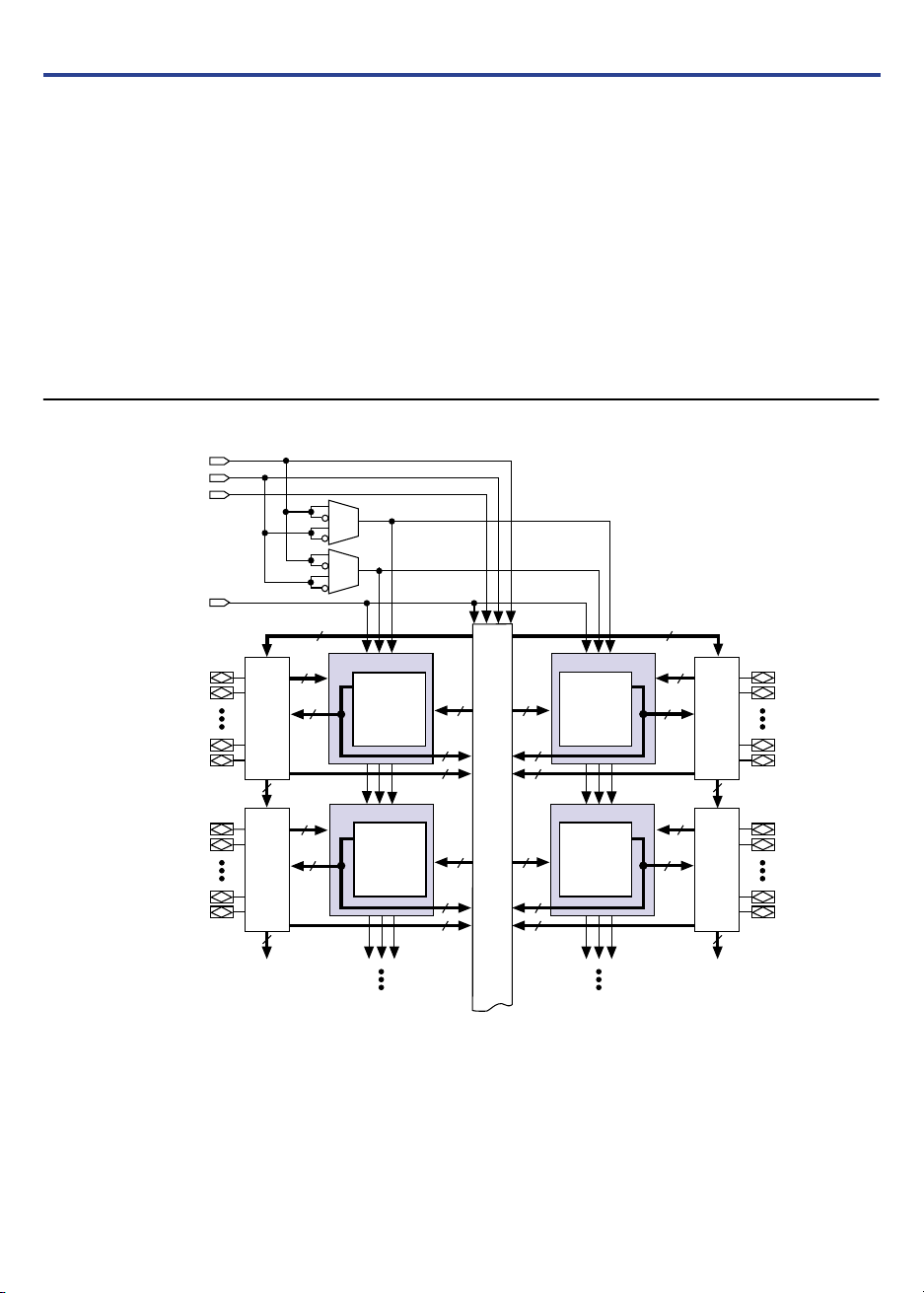
The MAX 7000A architecture includes four dedicated inputs that can be
used as general-purpose inputs or as high-speed, global control signals
(clock, clear, and two output enable signals) for each macrocell and I/O
pin. Figure 1 shows the architecture of MAX 7000A devices.
Figure 1. MAX 7000A Device Block Diagram
INPUT/GCLK1
INPUT/OE2/GCLK2
INPUT/OE1
INPUT/GCLRn
6 or 10 Output Enables
2 to 16 I/O
I/O
Control
Block
2 to 16
2 to 16
(1)
LAB A
Macrocells
1 to 16
36 36
16
6 or 10 Output Enables
LAB B
2 to 16
Macrocells
17 to 32
16
2 to 16
Control
I/O
Block
(1)
2 to 16 I/O
PIA
2 to 16
16
2 to 16
Macrocells
49 to 64
LAB D
2 to 16
2 to 16
I/O
Control
Block
6
2 to 16 I/O
6
2 to 16 I/O
I/O
Control
Block
6
LAB C
2 to 16
2 to 16
6
Macrocells
33 to 48
2 to 16
36 36
16
2 to 16
Note:
(1) EPM7032AE, EPM7064AE, EPM7128A, EPM7128AE, EPM7256A, and EPM7256AE devices have six output enables.
EPM7512AE devices have 10 output enables.
6 Altera Corporation
Page 7
Logic Array Blocks
The MAX 7000A device architecture is based on the linking of
high-performance LABs. LABs consist of 16-macrocell arrays, as shown in
Figure 1. Multiple LABs are linked together via the PIA, a global bus that
is fed by all dedicated input pins, I/O pins, and macrocells.
Each LAB is fed by the following signals:
■
■
■
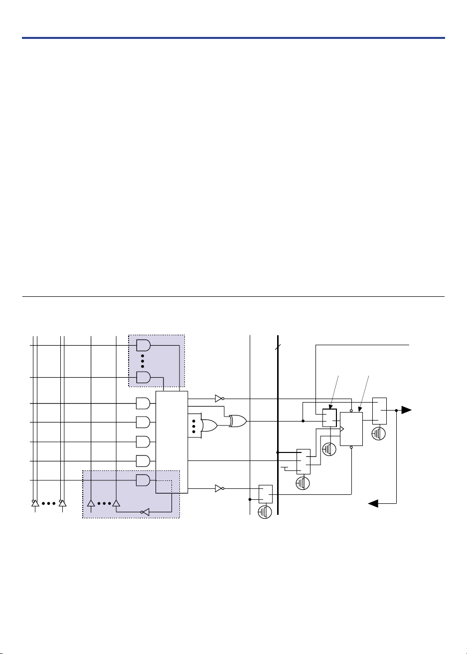
Macrocells
MAX 7000A macrocells can be individually configured for either
sequential or combinatorial logic operation. The macrocells consist of
three functional blocks: the logic array, the product-term select matrix,
and the programmable register. Figure 2 shows a MAX 7000A macrocell.
Figure 2. MAX 7000A Macrocell
LAB Local Array
MAX 7000A Programmable Logic Device Family Data Sheet
36 signals from the PIA that are used for general logic inputs
Global controls that are used for secondary register functions
Direct input paths from I/O pins to the registers that are used for fast
setup times
Global
Global
Clear
Product-
Te r m
Select
Matrix
Parallel Logic
Expanders
(from other
macrocells)
Clear
Select
Clocks
2
VCC
Clock/
Enable
Select
Fast Input
Select
D/T Q
ENA
PRN
CLRN
Programmable
Register
Register
Bypass
From
I/O pin
To I/O
Control
Block
To PIA
36 Signals
from PIA
16 Expander
Product Terms
Shared Logic
Expanders
Altera Corporation 7
Page 8

MAX 7000A Programmable Logic Device Family Data Sheet
Combinatorial logic is implemented in the logic array, which provides
five product terms per macrocell. The product-term select matrix allocates
these product terms for use as either primary logic inputs (to the OR and
XOR gates) to implement combinatorial functions, or as secondary inputs
to the macrocell’s register preset, clock, and clock enable control
functions.
Two kinds of expander product terms (“expanders”) are available to
supplement macrocell logic resources:
■ Shareable expanders, which are inverted product terms that are fed
back into the logic array
■ Parallel expanders, which are product terms borrowed from adjacent
macrocells
The Altera development system automatically optimizes product-term
allocation according to the logic requirements of the design.
For registered functions, each macrocell flipflop can be individually
programmed to implement D, T, JK, or SR operation with programmable
clock control. The flipflop can be bypassed for combinatorial operation.
During design entry, the designer specifies the desired flipflop type; the
MAX+PLUS II software then selects the most efficient flipflop operation
for each registered function to optimize resource utilization.
Each programmable register can be clocked in three different modes:
■ Global clock signal. This mode achieves the fastest clock-to-output
performance.
■ Global clock signal enabled by an active-high clock enable. A clock
enable is generated by a product term. This mode provides an enable
on each flipflop while still achieving the fast clock-to-output
performance of the global clock.
■ Array clock implemented with a product term. In this mode, the
flipflop can be clocked by signals from buried macrocells or I/O pins.
Two global clock signals are available in MAX 7000A devices. As shown
in Figure 1, these global clock signals can be the true or the complement
of either of the global clock pins, GCLK1 or GCLK2.
8 Altera Corporation
Page 9

MAX 7000A Programmable Logic Device Family Data Sheet
Each register also supports asynchronous preset and clear functions. As
shown in Figure 2, the product-term select matrix allocates product terms
to control these operations. Although the product-term-driven preset and
clear from the register are active high, active-low control can be obtained
by inverting the signal within the logic array. In addition, each register
clear function can be individually driven by the active-low dedicated
global clear pin (GCLRn). Upon power-up, each register in a MAX 7000AE
device may be set to either a high or low state. This power-up state is
specified at design entry.
All MAX 7000A I/O pins have a fast input path to a macrocell register.
This dedicated path allows a signal to bypass the PIA and combinatorial
logic and be clocked to an input D flipflop with an extremely fast (as low
as 2.5 ns) input setup time.
Expander Product Terms
Although most logic functions can be implemented with the five product
terms available in each macrocell, more complex logic functions require
additional product terms. Another macrocell can be used to supply the
required logic resources. However, the MAX 7000A architecture also
offers both shareable and parallel expander product terms that provide
additional product terms directly to any macrocell in the same LAB. These
expanders help ensure that logic is synthesized with the fewest possible
logic resources to obtain the fastest possible speed.
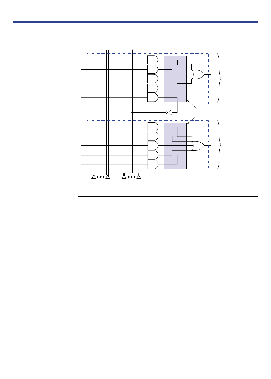
Shareable Expanders
Each LAB has 16 shareable expanders that can be viewed as a pool of
uncommitted single product terms (one from each macrocell) with
inverted outputs that feed back into the logic array. Each shareable
expander can be used and shared by any or all macrocells in the LAB to
build complex logic functions. A small delay (t
shareable expanders are used. Figure 3 shows how shareable expanders
can feed multiple macrocells.
Altera Corporation 9
) is incurred when
SEXP
Page 10
MAX 7000A Programmable Logic Device Family Data Sheet
Figure 3. MAX 7000A Shareable Expanders
Shareable expanders can be shared by any or all macrocells in an LAB.
Macrocell
Product-Term
Logic
Product-Term Select Matrix
Macrocell
Product-Term
Logic
36 Signals
from PIA
16 Shared
Expanders
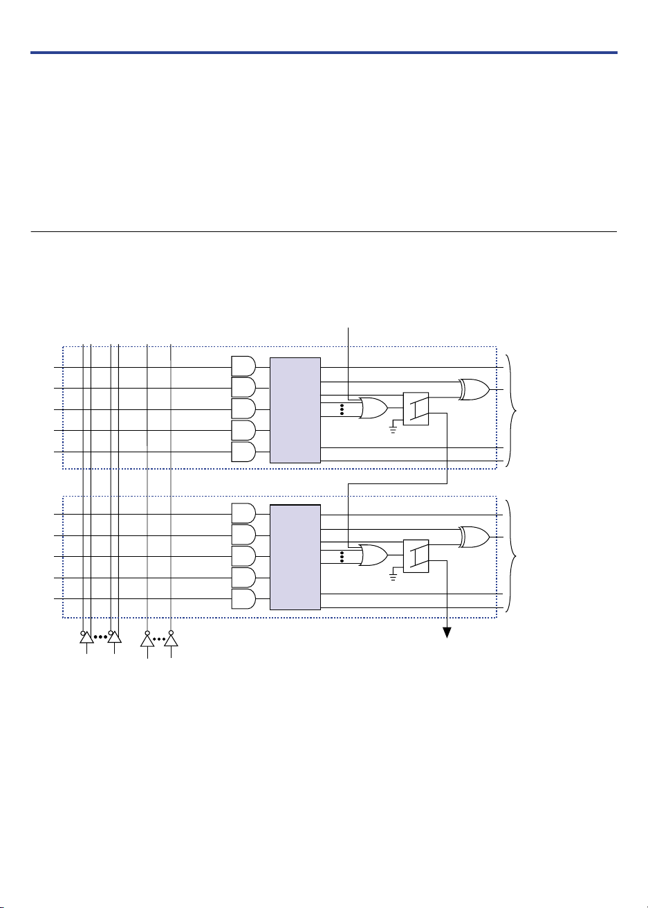
Parallel Expanders
Parallel expanders are unused product terms that can be allocated to a
neighboring macrocell to implement fast, complex logic functions.
Parallel expanders allow up to 20 product terms to directly feed the
macrocell OR logic, with five product terms provided by the macrocell and
15 parallel expanders provided by neighboring macrocells in the LAB.
The compiler can allocate up to three sets of up to five parallel expanders
to the macrocells that require additional product terms. Each set of five
parallel expanders incurs a small, incremental timing delay (t
example, if a macrocell requires 14 product terms, the Compiler uses the
five dedicated product terms within the macrocell and allocates two sets
of parallel expanders; the first set includes five product terms, and the
second set includes four product terms, increasing the total delay by 2 ×
t
.
PEXP
PEXP
). For
10 Altera Corporation
Page 11
MAX 7000A Programmable Logic Device Family Data Sheet
Two groups of eight macrocells within each LAB (e.g., macrocells 1
through 8 and 9 through 16) form two chains to lend or borrow parallel
expanders. A macrocell borrows parallel expanders from lowernumbered macrocells. For example, macrocell 8 can borrow parallel
expanders from macrocell 7, from macrocells 7 and 6, or from macrocells
7, 6, and 5. Within each group of eight, the lowest-numbered macrocell
can only lend parallel expanders, and the highest-numbered macrocell
can only borrow them. Figure 4 shows how parallel expanders can be
borrowed from a neighboring macrocell.
Figure 4. MAX 7000A Parallel Expanders
Unused product terms in a macrocell can be allocated to a neighboring macrocell.
From
Previous
Macrocell
Preset
36 Signals
from PIA
16 Shared
Expanders
Product-
Te r m
Select
Matrix
Product-
Te r m
Select
Matrix
Macrocell
ProductTerm Logic
Clock
Clear
Preset
Macrocell
ProductTerm Logic
Clock
Clear
To Next
Macrocell
Altera Corporation 11
Page 12
MAX 7000A Programmable Logic Device Family Data Sheet
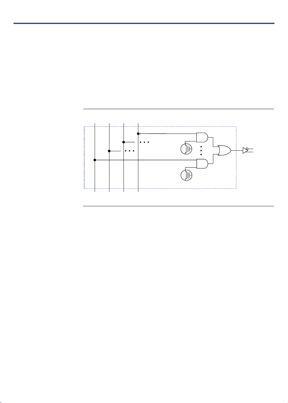
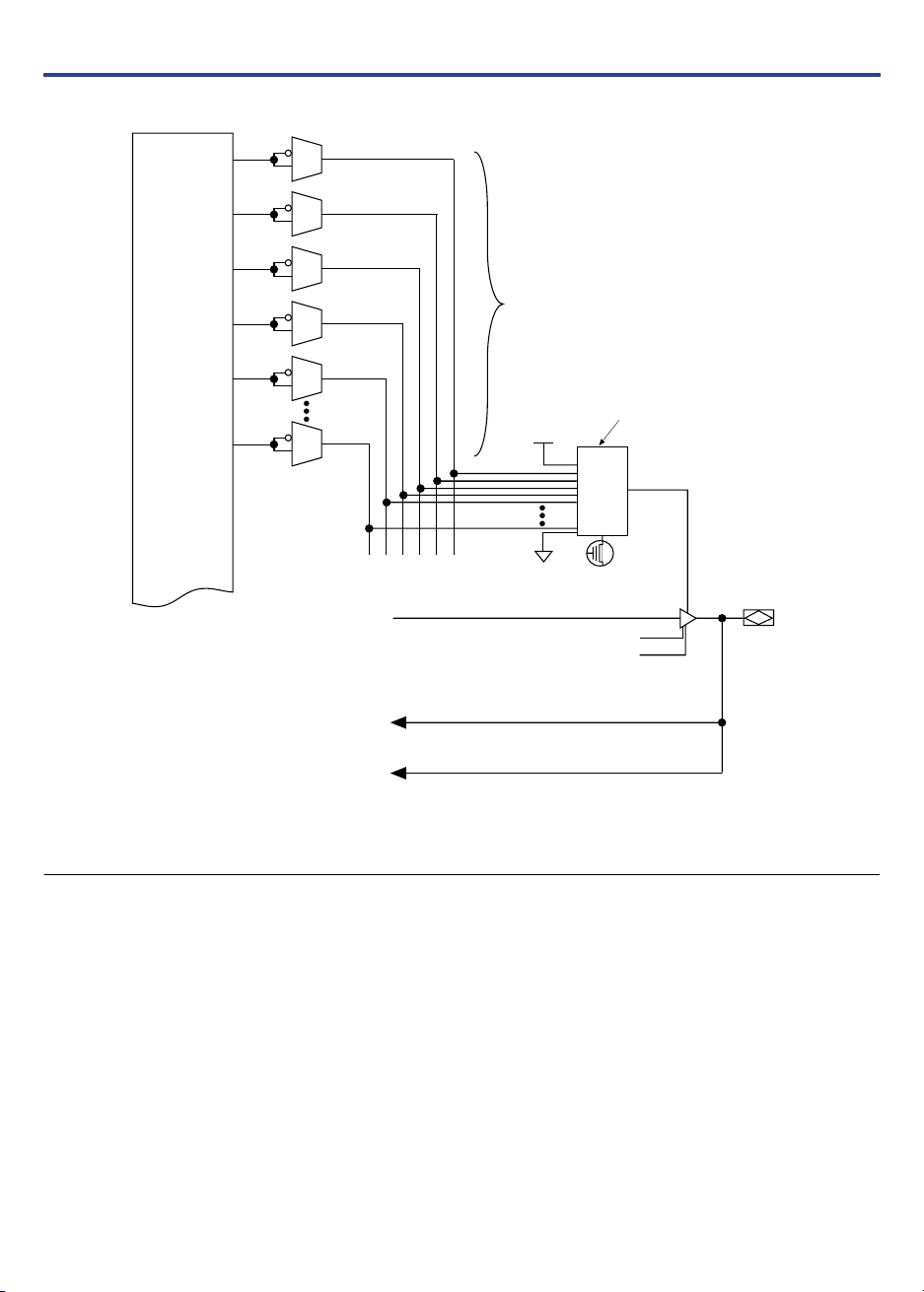
Programmable Interconnect Array
Logic is routed between LABs on the PIA. This global bus is a
programmable path that connects any signal source to any destination on
the device. All MAX 7000A dedicated inputs, I/O pins, and macrocell
outputs feed the PIA, which makes the signals available throughout the
entire device. Only the signals required by each LAB are actually routed
from the PIA into the LAB. Figure 5 shows how the PIA signals are routed
into the LAB. An EEPROM cell controls one input to a 2-input AND gate,
which selects a PIA signal to drive into the LAB.
Figure 5. MAX 7000A PIA Routing
To LAB
PIA Signals
While the routing delays of channel-based routing schemes in masked or
field-programmable gate arrays (FPGAs) are cumulative, variable, and
path-dependent, the MAX 7000A PIA has a predictable delay. The PIA
makes a design’s timing performance easy to predict.
I/O Control Blocks
The I/O control block allows each I/O pin to be individually configured
for input, output, or bidirectional operation. All I/O pins have a tri-state
buffer that is individually controlled by one of the global output enable
signals or directly connected to ground or VCC. Figure 6 shows the I/O
control block for MAX 7000A devices. The I/O control block has 6 or
10 global output enable signals that are driven by the true or complement
of two output enable signals, a subset of the I/O pins, or a subset of the
I/O macrocells.
12 Altera Corporation
Page 13
MAX 7000A Programmable Logic Device Family Data Sheet
Figure 6. I/O Control Block of MAX 7000A Devices
6 or 10 Global
Output Enable Signals
(1)
PIA
OE Select Multiplexer
To Other I/O Pins
From
Macrocell
Fast Input to
Macrocell
Register
To PIA
VCC
GND
Open-Drain Output
Slew-Rate Control
Note:
(1) EPM7032AE, EPM7064AE, EPM7128A, EPM7128AE, EPM7256A, and EPM7256AE devices have six output enable
signals. EPM7512AE devices have 10 output enable signals.
When the tri-state buffer control is connected to ground, the output is
tri-stated (high impedance) and the I/O pin can be used as a dedicated
input. When the tri-state buffer control is connected to VCC, the output is
enabled.
The MAX 7000A architecture provides dual I/O feedback, in which
macrocell and pin feedbacks are independent. When an I/O pin is
configured as an input, the associated macrocell can be used for buried
logic.
Altera Corporation 13
Page 14

MAX 7000A Programmable Logic Device Family Data Sheet
SameFrame Pin-Outs
MAX 7000A devices support the SameFrame pin-out feature for
FineLine BGA packages. The SameFrame pin-out feature is the
arrangement of balls on FineLine BGA packages such that the lower-ballcount packages form a subset of the higher-ball-count packages.
SameFrame pin-outs provide the flexibility to migrate not only from
device to device within the same package, but also from one package to
another. A given printed circuit board (PCB) layout can support multiple
device density/package combinations. For example, a single board layout
can support a range of devices from an EPM7128AE device in a 100-pin
FineLine BGA package to an EPM7512AE device in a 256-pin
FineLine BGA package.
The Altera design software provides support to design PCBs with
SameFrame pin-out devices. Devices can be defined for present and
future use. The software generates pin-outs describing how to lay out a
board to take advantage of this migration (see Figure 7).
Figure 7. SameFrame Pin-Out Example
Printed Circuit Board
Designed for 256-Pin FineLine BGA Package
100-Pin
FineLine
BGA
100-Pin FineLine BGA Package
(Reduced I/O Count or
Logic Requirements)
14 Altera Corporation
256-Pin FineLine BGA Package
(Increased I/O Count or
Logic Requirements)
256-Pin
FineLine
BGA
Page 15

MAX 7000A Programmable Logic Device Family Data Sheet
In-System
Programmability (ISP)
MAX 7000A devices can be programmed in-system via an industrystandard 4-pin IEEE Std. 1149.1 (JTAG) interface. ISP offers quick, efficient
iterations during design development and debugging cycles. The
MAX 7000A architecture internally generates the high programming
voltages required to program EEPROM cells, allowing in-system
programming with only a single 3.3-V power supply. During in-system
programming, the I/O pins are tri-stated and weakly pulled-up to
eliminate board conflicts. The pull-up value is nominally 50 kΩ.
MAX 7000AE devices have an enhanced ISP algorithm for faster
programming. These devices also offer an ISP_Done bit that provides safe
operation when in-system programming is interrupted. This ISP_Done
bit, which is the last bit programmed, prevents all I/O pins from driving
until the bit is programmed. This feature is available in EPM7032AE,
EPM7064AE, EPM7128AE, EPM7256AE, and EPM7512AE devices only.
ISP simplifies the manufacturing flow by allowing devices to be mounted
on a printed circuit board (PCB) with standard pick-and-place equipment
before they are programmed. MAX 7000A devices can be programmed by
downloading the information via in-circuit testers, embedded processors,
the Altera BitBlaster serial download cable, ByteBlaster parallel port
download cable, ByteBlasterMV parallel port download cable, and
MasterBlaster serial/USB communications cable. Programming the
devices after they are placed on the board eliminates lead damage on
high-pin-count packages (e.g., QFP packages) due to device handling.
MAX 7000A devices can be reprogrammed after a system has already
shipped to the field. For example, product upgrades can be performed in
the field via software or modem.
In-system programming can be accomplished with either an adaptive or
constant algorithm. An adaptive algorithm reads information from the
unit and adapts subsequent programming steps to achieve the fastest
possible programming time for that unit. A constant algorithm uses a predefined (non-adaptive) programming sequence that does not take
advantage of adaptive algorithm programming time improvements.
Some in-circuit testers cannot program using an adaptive algorithm.
Therefore, a constant algorithm must be used. MAX 7000AE devices can
be programmed with either an adaptive or constant (non-adaptive)
algorithm. EPM7128A and EPM7256A device can only be programmed
with an adaptive algorithm; users programming these two devices on
platforms that cannot use an adaptive algorithm should use EPM7128AE
and EPM7256AE devices.
The Jam programming and test language can be used to program
MAX 7000A devices with in-circuit testers, PCs, or embedded processors.
Altera Corporation 15
Page 16

MAX 7000A Programmable Logic Device Family Data Sheet
f
Programming with External Hardware
f
f
IEEE Std.
1149.1 (JTAG)
Boundary-Scan
Support
For more information on using the Jam STAPL language, see Application
Note 88 (Using the Jam Language for ISP & ICR via an Embedded Processor)
and Application Note 122 (Using Jam STAPL for ISP & ICR via an Embedded
Processor).
MAX 7000A devices can be programmed on Windows-based PCs with an
Altera Logic Programmer card, the MPU, and the appropriate device
adapter. The MPU performs continuity checks to ensure adequate
electrical contact between the adapter and the device.
For more information, see the Altera Programming Hardware Data Sheet.
The MAX+PLUS II software can use text- or waveform-format test vectors
created with the MAX+PLUS II Text Editor or Waveform Editor to test the
programmed device. For added design verification, designers can
perform functional testing to compare the functional device behavior with
the results of simulation.
Data I/O, BP Microsystems, and other programming hardware
manufacturers provide programming support for Altera devices.
For more information, see Programming Hardware Manufacturers.
MAX 7000A devices include the JTAG BST circuitry defined by IEEE Std.
1149.1. Table 5 describes the JTAG instructions supported by MAX 7000A
devices. The pin-out tables starting on page 52 of this data sheet show the
location of the JTAG control pins for each device. If the JTAG interface is
not required, the JTAG pins are available as user I/O pins.
16 Altera Corporation
Page 17

MAX 7000A Programmable Logic Device Family Data Sheet
Table 5. MAX 7000A JTAG Instructions
JTAG Instruction Description
SAMPLE/PRELOAD Allows a snapshot of signals at the device pins to be captured and examined during
normal device operation, and permits an initial data pattern output at the device pins
EXTEST Allows the external circuitry and board-level interconnections to be tested by forcing a
test pattern at the output pins and capturing test results at the input pins
BYPASS Places the 1-bit bypass register between the TDI and TDO pins, which allows the BST
data to pass synchronously through a selected device to adjacent devices during normal
device operation
IDCODE Selects the IDCODE register and places it between the TDI and TDO pins, allowing the
IDCODE to be serially shifted out of TDO
USERCODE Selects the 32-bit USERCODE register and places it between the TDI and TDO pins,
allowing the USERCODE value to be shifted out of TDO. The USERCODE instruction is
available for MAX 7000AE devices only
UESCODE These instructions select the user electronic signature (UESCODE) and allow the
UESCODE to be shifted out of TDO. UESCODE instructions are available for EPM7128A
and EPM7256A devices only.
ISP Instructions These instructions are used when programming MAX 7000A devices via the JTAG ports
with the BitBlaster, ByteBlaster, ByteBlasterMV, or MasterBlaster download cable, or
using a Jam STAPL File, JBC File, or SVF File via an embedded processor or test
equipment.
Altera Corporation 17
Page 18

MAX 7000A Programmable Logic Device Family Data Sheet
The instruction register length of MAX 7000A devices is 10 bits. The user
electronic signature (UES) register length in MAX 7000A devices is 16 bits.
The MAX 7000AE USERCODE register length is 32 bits. Tables 6 and 7
show the boundary-scan register length and device IDCODE information
for MAX 7000A devices.
Table 6. MAX 7000A Boundary-Scan Register Length
Device Boundary-Scan Register Length
EPM7032AE 96
EPM7064AE 192
EPM7128A 288
EPM7128AE 288
EPM7256A 480
EPM7256AE 480
EPM7512AE 624
Table 7. 32-Bit MAX 7000A Device IDCODE Note (1)
Device IDCODE (32 Bits)
f
Version
(4 Bits)
EPM7032AE 0001 0111 0000 0011 0010 00001101110 1
EPM7064AE 0001 0111 0000 0110 0100 00001101110 1
EPM7128A 0000 0111 0001 0010 1000 00001101110 1
EPM7128AE 0001 0111 0001 0010 1000 00001101110 1
EPM7256A 0000 0111 0010 0101 0110 00001101110 1
EPM7256AE 0001 0111 0010 0101 0110 00001101110 1
EPM7512AE 0001 0111 0101 0001 0010 00001101110 1
Notes:
(1) The most significant bit (MSB) is on the left.
(2) The least significant bit (LSB) for all JTAG IDCODEs is 1.
Part Number (16 Bits) Manufacturer’s
Identity (11 Bits)
1 (1 Bit)
(2)
See Application Note 39 (IEEE 1149.1 (JTAG) Boundary-Scan Testing in Altera
Devices) for more information on JTAG BST.
18 Altera Corporation
Page 19
MAX 7000A Programmable Logic Device Family Data Sheet
Figure 8 shows timing information for the JTAG signals.
Figure 8. MAX 7000A JTAG Waveforms
TMS
TDI
t
JCP
t
JCL
t
JPSU
t
JPH
TCK
t
JCH
t
JPXZ
TDO
Signal
to Be
Captured
Signal
to Be
Driven
t
JPZX
t
JSZX
t
JSSU
t
JPCO
t
JSH
t
JSCO
t
JSXZ
Table 8 shows the JTAG timing parameters and values for MAX 7000A
devices.
Table 8. JTAG Timing Parameters & Values for MAX 7000A Devices Note (1)
Symbol Parameter Min Max Unit
t
JCP
t
JCH
t
JCL
t
JPSU
t
JPH
t
JPCO
t
JPZX
t
JPXZ
t
JSSU
t
JSH
t
JSCO
t
JSZX
t
JSXZ
TCK clock period 100 ns
TCK clock high time 50 ns
TCK clock low time 50 ns
JTAG port setup time 20 ns
JTAG port hold time 45 ns
JTAG port clock to output 25 ns
JTAG port high impedance to valid output 25 ns
JTAG port valid output to high impedance 25 ns
Capture register setup time 20 ns
Capture register hold time 45 ns
Update register clock to output 25 ns
Update register high impedance to valid output 25 ns
Update register valid output to high impedance 25 ns
Note:
(1) Timing parameters shown in this table apply for all specified VCCIO levels.
Altera Corporation 19
Page 20

MAX 7000A Programmable Logic Device Family Data Sheet
Programmable Speed/Power Control
Output
Configuration
MAX 7000A devices offer a power-saving mode that supports low-power
operation across user-defined signal paths or the entire device. This
feature allows total power dissipation to be reduced by 50% or more
because most logic applications require only a small fraction of all gates to
operate at maximum frequency.
The designer can program each individual macrocell in a MAX 7000A
device for either high-speed (i.e., with the Turbo Bit option turned on) or
low-power operation (i.e., with the Turbo Bit option turned off). As a
result, speed-critical paths in the design can run at high speed, while the
remaining paths can operate at reduced power. Macrocells that run at low
power incur a nominal timing delay adder (t
tEN, t
MAX 7000A device outputs can be programmed to meet a variety of
system-level requirements.
SEXP
, t
ACL
, and t
parameters.
CPPW
) for the t
LPA
LAD
, t
LAC
, tIC,
MultiVolt I/O Interface
The MAX 7000A device architecture supports the MultiVolt I/O interface
feature, which allows MAX 7000A devices to connect to systems with
differing supply voltages. MAX 7000A devices in all packages can be set
for 2.5-V, 3.3-V, or 5.0-V I/O pin operation. These devices have one set of
VCC pins for internal operation and input buffers (VCCINT), and another
set for I/O output drivers (VCCIO).
The VCCIO pins can be connected to either a 3.3-V or 2.5-V power supply,
depending on the output requirements. When the VCCIO pins are
connected to a 2.5-V power supply, the output levels are compatible with
2.5-V systems. When the VCCIO pins are connected to a 3.3-V power
supply, the output high is at 3.3 V and is therefore compatible with 3.3-V
or 5.0-V systems. Devices operating with V
incur a slightly greater timing delay of t
always be driven by 2.5-V, 3.3-V, or 5.0-V signals.
Table 9 describes the MAX 7000A MultiVolt I/O support.
Table 9. MAX 7000A MultiVolt I/O Support
V
Voltage Input Signal (V) Output Signal (V)
CCIO
2.5 3.3 5.0 2.5 3.3 5.0
2.5
3.3
20 Altera Corporation
vvvv
vvv vv
OD2
levels lower than 3.0 V
CCIO
instead of t
. Inputs can
OD1
Page 21

MAX 7000A Programmable Logic Device Family Data Sheet
Open-Drain Output Option
MAX 7000A devices provide an optional open-drain (equivalent to
open-collector) output for each I/O pin. This open-drain output enables
the device to provide system-level control signals (e.g., interrupt and
write enable signals) that can be asserted by any of several devices. It can
also provide an additional wired-OR plane.
Open-drain output pins on MAX 7000A devices (with a pull-up resistor to
the 5.0-V supply) can drive 5.0-V CMOS input pins that require a V
3.5 V. When the open-drain pin is active, it will drive low. When the pin
is inactive, the trace will be pulled up to 5.0 V by the resistor. The opendrain pin will only drive low or tri-state; it will never drive high. The rise
time is dependent on the value of the pull-up resistor and load
impedance. The IOL current specification should be considered when
selecting a pull-up resistor.
IH
of
Programmable Ground Pins
Each unused I/O pin on MAX 7000A devices may be used as an
additional ground pin. In EPM7128A and EPM7256A devices, utilizing
unused I/O pins as additional ground pins requires using the associated
macrocell. In MAX 7000AE devices, this programmable ground feature
does not require the use of the associated macrocell; therefore, the buried
macrocell is still available for user logic.
Slew-Rate Control
The output buffer for each MAX 7000A I/O pin has an adjustable output
slew rate that can be configured for low-noise or high-speed performance.
A faster slew rate provides high-speed transitions for high-performance
systems. However, these fast transitions may introduce noise transients
into the system. A slow slew rate reduces system noise, but adds a
nominal delay of 4 to 5 ns. When the configuration cell is turned off, the
slew rate is set for low-noise performance. Each I/O pin has an individual
EEPROM bit that controls the slew rate, allowing designers to specify the
slew rate on a pin-by-pin basis. The slew rate control affects both the
rising and falling edges of the output signal.
Altera Corporation 21
Page 22
MAX 7000A Programmable Logic Device Family Data Sheet
CC
Power Sequencing & Hot-Socketing
Design Security
Generic Testing
Because MAX 7000A devices can be used in a mixed-voltage
environment, they have been designed specifically to tolerate any possible
power-up sequence. The V
CCIO
and V
power planes can be powered
CCINT
in any order.
Signals can be driven into MAX 7000AE devices before and during powerup without damaging the device. Additionally, MAX 7000AE devices do
not drive out during power-up. Once operating conditions are reached,
MAX 7000AE devices operate as specified by the user.
All MAX 7000A devices contain a programmable security bit that controls
access to the data programmed into the device. When this bit is
programmed, a design implemented in the device cannot be copied or
retrieved. This feature provides a high level of design security because
programmed data within EEPROM cells is invisible. The security bit that
controls this function, as well as all other programmed data, is reset only
when the device is reprogrammed.
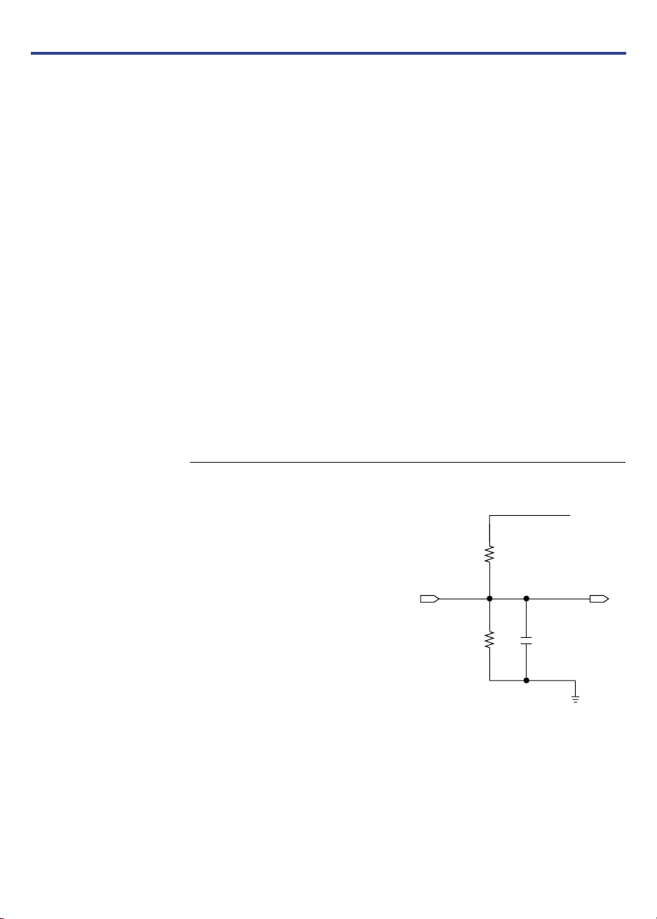
MAX 7000A devices are fully tested. Complete testing of each
programmable EEPROM bit and all internal logic elements ensures 100%
programming yield. AC test measurements are taken under conditions
equivalent to those shown in Figure 9. Test patterns can be used and then
erased during early stages of the production flow.
Figure 9. MAX 7000A AC Test Conditions
Power supply transients can affect AC
measurements. Simultaneous transitions
of multiple outputs should be avoided for
accurate measurement. Threshold tests
must not be performed under AC
conditions. Large-amplitude, fast-groundcurrent transients normally occur as the
device outputs discharge the load
capacitances. When these transients flow
through the parasitic inductance between
the device ground pin and the test system
ground, significant reductions in
observable noise immunity can result.
Numbers in brackets are for 2.5-V
outputs. Numbers without brackets are for
3.3-V outputs.
703 Ω
[521 Ω]
Device
Output
586 Ω
[481 Ω]
Device input
rise and fall
times < 2 ns
C1 (includes JIG
capacitance)
V
To Test
System
22 Altera Corporation
Page 23
MAX 7000A Programmable Logic Device Family Data Sheet
Operating Conditions
Tables 10 through 13 provide information on absolute maximum ratings,
recommended operating conditions, operating conditions, and
capacitance for MAX 7000A devices.
Table 10. MAX 7000A Device Absolute Maximum Ratings Note (1)
Symbol Parameter Conditions Min Max Unit
V
V
I
OUT
T
T
T
CC
I
STG
A
J
Supply voltage With respect to ground (2) –0.5 4.6 V
DC input voltage –2.0 5.75 V
DC output current, per pin –25 25 mA
Storage temperature No bias –65 150 ° C
Ambient temperature Under bias –65 135 ° C
Junction temperature BGA, FineLine BGA, PQFP, and
135 ° C
TQFP packages, under bias
Table 11. MAX 7000A Device Recommended Operating Conditions
Symbol Parameter Conditions Min Max Unit
V
CCINT
V
CCIO
V
CCISP
V
I
V
O
T
A
T
J
t
R
t
F
Supply voltage for internal logic
(3) 3.0 3.6 V
and input buffers
Supply voltage for output
(3) 3.0 3.6 V
drivers, 3.3-V operation
Supply voltage for output
(3) 2.3 2.7 V
drivers, 2.5-V operation
Supply voltage during in-
3.0 3.6 V
system programming
Input voltage (4) –0.5 5.75 V
Output voltage 0 V
CCIO
Ambient temperature For commercial use 0 70 ° C
For industrial use –40 85 ° C
Junction temperature For commercial use 0 90 ° C
For industrial use –40 105 ° C
Input rise time 40 ns
Input fall time 40 ns
V
Altera Corporation 23
Page 24
MAX 7000A Programmable Logic Device Family Data Sheet
Table 12. MAX 7000A Device DC Operating Conditions Note (5)
Symbol Parameter Conditions Min Max Unit
V
V
V
V
I
I
I
OZ
R
High-level input voltage 1.7 5.75 V
IH
Low-level input voltage –0.5 0.8 V
IL
3.3-V high-level TTL output
OH
IOH = –8 mA DC, V
= 3.00 V (6) 2.4 V
CCIO
voltage
3.3-V high-level CMOS output
voltage
2.5-V high-level output voltage I
I
= –0.1 mA DC, V
OH
(6)
= –100 µA DC, V
OH
CCIO
CCIO
= 3.00 V
= 2.30 V
V
– 0.2 V
CCIO
2.1 V
(6)
I
3.3-V low-level TTL output
OL
= –1 mA DC, V
OH
= –2 mA DC, V
I
OH
IOL = 8 mA DC, V
= 2.30 V (6) 2.0 V
CCIO
= 2.30 V (6) 1.7 V
CCIO
= 3.00 V (7) 0.45 V
CCIO
voltage
3.3-V low-level CMOS output
I
= 0.1 mA DC, V
OL
= 3.00 V (7) 0.2 V
CCIO
voltage
2.5-V low-level output voltage I
= 100 µA DC, V
OL
I
= 1 mA DC, V
OL
= 2 mA DC, V
I
OL
Input leakage current VI = V
Tri-state output off-state
VO = V
or ground –10 10 µA
CCINT
or ground –10 10 µA
CCINT
= 2.30 V (7) 0.2 V
CCIO
= 2.30 V (7) 0.4 V
CCIO
= 2.30 V (7) 0.7 V
CCIO
current
Value of I/O pin pull-up resistor
ISP
during in-system programming
or during power-up
V
= 3.0 to 3.6 V (8) 20 50 kΩ
CCIO
= 2.3 to 2.7 V (8) 30 80 kΩ
V
CCIO
= 2.3 to 3.6 V (9) 20 74 kΩ
V
CCIO
Table 13. MAX 7000A Device Capacitance Note (10)
Symbol Parameter Conditions Min Max Unit
C
C
24 Altera Corporation
Input pin capacitance VIN = 0 V, f = 1.0 MHz 8 pF
IN
I/O pin capacitance V
I/O
= 0 V, f = 1.0 MHz 8 pF
OUT
Page 25

MAX 7000A Programmable Logic Device Family Data Sheet
Notes to tables:
(1) See the Operating Requirements for Altera Devices Data Sheet.
(2) Minimum DC input voltage is –0.5 V. During transitions, the inputs may undershoot to –2.0 V for input currents
less than 100 mA and periods shorter than 20 ns.
(3) For EPM7128A and EPM7256A devices only, V
(4) In MAX 7000AE devices, all pins, including dedicated inputs, I/O pins, and JTAG pins, may be driven before
and V
V
CCINT
(5) These values are specified under the recommended operating conditions shown in Table 11 on page 23.
are powered.
CCIO
(6) The parameter is measured with 50% of the outputs each sourcing the specified current. The I
to high-level TTL or CMOS output current.
(7) The parameter is measured with 50% of the outputs each sinking the specified current. The I
low-level TTL or CMOS output current.
must rise monotonically.
CC
parameter refers
OH
parameter refers to
OL
(8) For EPM7128A and EPM7256A devices, this pull-up exists while a device is programmed in-system.
(9) For MAX 7000AE devices, this pull-up exists while devices are programmed in-system and in unprogrammed
devices during power-up.
(10) Capacitance is measured at 25 °C and is sample-tested only. The
OE1 pin (high-voltage pin during programming)
has a maximum capacitance of 20 pF.
Altera Corporation 25
Page 26

MAX 7000A Programmable Logic Device Family Data Sheet
Figure 10 shows the typical output drive characteristics of MAX 7000A
devices.
Figure 10. Output Drive Characteristics of MAX 7000A Devices
Typical I
O
Output
Current (mA)
Typical I
O
Output
Current (mA)
MAX 7000AE Devices
150
I
OL
100
50
0
0
1234
VO Output Voltage (V)
EPM7128A & EPM7256A Devices
120
I
OL
80
40
0
0
1234
VO Output Voltage (V)
V
= 3.3
CCINT
= 3.3 V
V
CCIO
Temperature
I
OH
V
= 3.3 V
CCINT
= 3.3 V
V
CCIO
T
emperature
I
V
= 25 C
OH
O
O
= 25 C
2.5 V3.3 V
Typical I
Output
Current (mA)
5
2.5 V3.3 V
Typical I
Output
Current (mA)
5
MAX 7000AE Devices
150
I
OL
100
O
50
0
0
V
= 3.3 V
CCINT
= 2.5 V
V
CCIO
Temperature
1234
I
OH
O
= 25 C
5
VO Output Voltage (V)
EPM7128A & EPM7256A Devices
120
I
OL
80
O
40
0
1234
V
= 3.3 V
CCINT
= 2.5 V
V
CCIO
T
emperature
I
OH
O
= 25 C
5
VO Output Voltage (V)
Timing Model
MAX 7000A device timing can be analyzed with the Altera software, a
variety of popular industry-standard EDA simulators and timing
analyzers, or with the timing model shown in Figure 11. MAX 7000A
devices have predictable internal delays that enable the designer to
determine the worst-case timing of any design. The software provides
timing simulation, point-to-point delay prediction, and detailed timing
analysis for device-wide performance evaluation.
26 Altera Corporation
Page 27

Figure 11. MAX 7000A Timing Model
Input
Delay
t
IN
PIA
Delay
t
PIA
The timing characteristics of any signal path can be derived from the
timing model and parameters of a particular device. External timing
parameters, which represent pin-to-pin timing delays, can be calculated
as the sum of internal parameters. Figure 12 shows the timing relationship
between internal and external delay parameters.
MAX 7000A Programmable Logic Device Family Data Sheet
Internal Output
Enable Delay
t
IOE
Global Control
Delay
t
GLOB
Logic Array
Delay
t
LAD
Register
Control Delay
t
LAC
t
IC
t
EN
Shared
Expander Delay
t
SEXP
Parallel
Expander Delay
t
PEXP
Input Delay
Fast
t
FIN
Register
Delay
t
SU
t
H
t
PRE
t
CLR
t
RD
t
COMB
t
FSU
t
FH
Output
Delay
t
OD1
t
OD2
t
OD3
t
XZ
t
X1
Z
t
ZX2
t
ZX3
I/O
Delay
t
IO
f
See Application Note 94 (Understanding MAX 7000 Timing) for more
information.
Altera Corporation 27
Page 28

MAX 7000A Programmable Logic Device Family Data Sheet
Figure 12. MAX 7000A Switching Waveforms
tR & tF < 2 ns. Inputs are
driven at 3 V for a logic
high and 0 V for a logic
low. All timing
characteristics are
measured at 1.5 V.
Input Pin
I/O Pin
PIA Delay
Shared Expander
Parallel Expander
Delay
Logic Array
Input
Delay
Logic Array
Output
Output Pin
Global
Clock Pin
Global Clock
at Register
Data or Enable
(Logic Array Output)
Combinatorial Mode
t
IN
t
IO
Global Clock Mode
t
IN
tSUt
t
CH
t
GLOB
H
t
R
t
PIA
t
SEXP
t
, t
LAC
LAD
t
PEXP
t
COMB
t
OD
t
CL
t
F
Array Clock Mode
t
F
t
, t
CLR
PRE
t
OD
Input or I/O Pin
Clock into PIA
Clock into
Logic Array
Clock at
Register
Data from
Logic Array
Register to PIA
to Logic Array
Register Output
to Pin
t
R
t
ACH
t
IN
t
IO
t
PIA
t
ACL
t
IC
t
t
SU
H
t
RD
t
PIA
t
OD
28 Altera Corporation
t
PIA
Page 29

MAX 7000A Programmable Logic Device Family Data Sheet
Tables 14 through 27 show EPM7032AE, EPM7064AE, EPM7128AE,
EPM7256AE, EPM7512AE, EPM7128A, and EPM7256A timing
information.
Table 14. EPM7032AE External Timing Parameters
Symbol Parameter Conditions Speed Grade Unit
-4 -7 -10
Min Max Min Max Min Max
t
PD1
t
PD2
t
SU
t
H
t
FSU
t
FH
t
CO1
t
CH
t
CL
t
ASU
t
AH
t
ACO1
t
ACH
t
ACL
t
CPPW
t
CNT
f
CNT
t
ACNT
f
ACNT
Input to nonregistered output
I/O input to nonregistered output
Global clock setup
C1 = 35 pF
4.5 7.5 10 ns
(2)
C1 = 35 pF
4.5 7.5 10 ns
(2)
(2) 2.9 4.7 6.3 ns
time
Global clock hold time (2) 0.0 0.0 0.0 ns
Global clock setup
2.5 3.0 3.0 ns
time of fast input
Global clock hold time
0.0 0.0 0.0 ns
of fast input
Global clock to output
C1 = 35 pF 1.0 3.0 1.0 5.0 1.0 6.7 ns
delay
Global clock high time 2.0 3.0 4.0 ns
Global clock low time 2.0 3.0 4.0 ns
Array clock setup time (2) 1.6 2.5 3.6 ns
Array clock hold time (2) 0.3 0.5 0.5 ns
Array clock to output
delay
C1 = 35 pF
(2)
1.0 4.3 1.0 7.2 1.0 9.4 ns
Array clock high time 2.0 3.0 4.0 ns
Array clock low time 2.0 3.0 4.0 ns
Minimum pulse width
(3) 2.0 3.0 4.0 ns
for clear and preset
Minimum global clock
(2) 4.4 7.2 9.7 ns
period
Maximum internal
(2), (4) 227.3 138.9 103.1 MHz
global clock frequency
Minimum array clock
(2) 4.4 7.2 9.7 ns
period
Maximum internal
(2), (4) 227.3 138.9 103.1 MHz
array clock frequency
Altera Corporation 29
Page 30

MAX 7000A Programmable Logic Device Family Data Sheet
Table 15. EPM7032AE Internal Timing Parameters (Part 1 of 2)
Symbol Parameter Conditions Speed Grade Unit
-4 -7 -10
Min Max Min Max Min Max
t
IN
t
IO
t
FIN
t
SEXP
t
PEXP
t
LAD
t
LAC
t
IOE
t
OD1
t
OD2
t
OD3
t
ZX1
t
ZX2
t
ZX3
t
XZ
t
SU
t
H
t
FSU
t
FH
t
RD
t
COMB
Input pad and buffer delay 0.7 1.2 1.5 ns
I/O input pad and buffer
0.7 1.2 1.5 ns
delay
Fast input delay 2.3 2.8 3.4 ns
Shared expander delay 1.9 3.1 4.0 ns
Parallel expander delay 0.5 0.8 1.0 ns
Logic array delay 1.5 2.5 3.3 ns
Logic control array delay 0.6 1.0 1.2 ns
Internal output enable delay 0.0 0.0 0.0 ns
Output buffer and pad
C1 = 35 pF 0.8 1.3 1.8 ns
delay, slow slew rate = off
V
= 3.3 V
CCIO
Output buffer and pad
delay, slow slew rate = off
V
= 2.5 V
CCIO
Output buffer and pad
C1 = 35 pF
1.3 1.8 2.3 ns
(5)
C1 = 35 pF 5.8 6.3 6.8 ns
delay, slow slew rate = on
V
= 2.5 V or 3.3 V
CCIO
Output buffer enable delay,
C1 = 35 pF 4.0 4.0 5.0 ns
slow slew rate = off
V
= 3.3 V
CCIO
Output buffer enable delay,
slow slew rate = off
V
= 2.5 V
CCIO
Output buffer enable delay,
C1 = 35 pF
4.5 4.5 5.5 ns
(5)
C1 = 35 pF 9.0 9.0 10.0 ns
slow slew rate = on
V
= 3.3 V
CCIO
Output buffer disable delay C1 = 5 pF 4.0 4.0 5.0 ns
Register setup time 1.3 2.0 2.8 ns
Register hold time 0.6 1.0 1.3 ns
Register setup time of fast
1.0 1.5 1.5 ns
input
Register hold time of fast
1.5 1.5 1.5 ns
input
Register delay 0.7 1.2 1.5 ns
Combinatorial delay 0.6 1.0 1.3 ns
30 Altera Corporation
Page 31

MAX 7000A Programmable Logic Device Family Data Sheet
Table 15. EPM7032AE Internal Timing Parameters (Part 2 of 2)
Symbol Parameter Conditions Speed Grade Unit
-4 -7 -10
Min Max Min Max Min Max
t
IC
t
EN
t
GLOB
t
PRE
t
CLR
t
PIA
t
LPA
Array clock delay 1.2 2.0 2.5 ns
Register enable time 0.6 1.0 1.2 ns
Global control delay 0.8 1.3 1.9 ns
Register preset time 1.2 1.9 2.6 ns
Register clear time 1.2 1.9 2.6 ns
PIA delay (2) 0.9 1.5 2.1 ns
Low-power adder (6) 2.5 4.0 5.0 ns
Altera Corporation 31
Page 32

MAX 7000A Programmable Logic Device Family Data Sheet
Table 16. EPM7064AE External Timing Parameters
Symbol Parameter Conditions Speed Grade Unit
-4 -7 -10
Min Max Min Max Min Max
t
PD1
t
PD2
t
SU
t
H
t
FSU
t
FH
t
CO1
t
CH
t
CL
t
ASU
t
AH
t
ACO1
t
ACH
t
ACL
t
CPPW
t
CNT
f
CNT
t
ACNT
f
ACNT
Input to nonregistered output
I/O input to nonregistered output
Global clock setup
C1 = 35 pF
4.5 7.5 10.0 ns
(2)
C1 = 35 pF
4.5 7.5 10.0 ns
(2)
(2) 2.8 4.7 6.2 ns
time
Global clock hold time (2) 0.0 0.0 0.0 ns
Global clock setup
2.5 3.0 3.0 ns
time of fast input
Global clock hold time
0.0 0.0 0.0 ns
of fast input
Global clock to output
C1 = 35 pF 1.0 3.1 1.0 5.1 1.0 7.0 ns
delay
Global clock high time 2.0 3.0 4.0 ns
Global clock low time 2.0 3.0 4.0 ns
Array clock setup time (2) 1.6 2.6 3.6 ns
Array clock hold time (2) 0.3 0.4 0.6 ns
Array clock to output
delay
C1 = 35 pF
(2)
1.0 4.3 1.0 7.2 1.0 9.6 ns
Array clock high time 2.0 3.0 4.0 ns
Array clock low time 2.0 3.0 4.0 ns
Minimum pulse width
(3) 2.0 3.0 4.0 ns
for clear and preset
Minimum global clock
(2) 4.5 7.4 10.0 ns
period
Maximum internal
(2), (4) 222.2 135.1 100.0 MHz
global clock frequency
Minimum array clock
(2) 4.5 7.4 10.0 ns
period
Maximum internal
(2), (4) 222.2 135.1 100.0 MHz
array clock frequency
32 Altera Corporation
Page 33

MAX 7000A Programmable Logic Device Family Data Sheet
Table 17. EPM7064AE Internal Timing Parameters (Part 1 of 2)
Symbol Parameter Conditions Speed Grade Unit
-4 -7 -10
Min Max Min Max Min Max
t
IN
t
IO
t
FIN
t
SEXP
t
PEXP
t
LAD
t
LAC
t
IOE
t
OD1
t
OD2
t
OD3
t
ZX1
t
ZX2
t
ZX3
t
XZ
t
SU
t
H
t
FSU
t
FH
t
RD
t
COMB
Input pad and buffer delay 0.6 1.1 1.4 ns
I/O input pad and buffer
0.6 1.1 1.4 ns
delay
Fast input delay 2.5 3.0 3.7 ns
Shared expander delay 1.8 3.0 3.9 ns
Parallel expander delay 0.4 0.7 0.9 ns
Logic array delay 1.5 2.5 3.2 ns
Logic control array delay 0.6 1.0 1.2 ns
Internal output enable delay 0.0 0.0 0.0 ns
Output buffer and pad
C1 = 35 pF 0.8 1.3 1.8 ns
delay, slow slew rate = off
V
= 3.3 V
CCIO
Output buffer and pad
delay, slow slew rate = off
V
= 2.5 V
CCIO
Output buffer and pad
C1 = 35 pF
1.3 1.8 2.3 ns
(5)
C1 = 35 pF 5.8 6.3 6.8 ns
delay, slow slew rate = on
V
= 2.5 V or 3.3 V
CCIO
Output buffer enable delay,
C1 = 35 pF 4.0 4.0 5.0 ns
slow slew rate = off
V
= 3.3 V
CCIO
Output buffer enable delay,
slow slew rate = off
V
= 2.5 V
CCIO
Output buffer enable delay,
C1 = 35 pF
4.5 4.5 5.5 ns
(5)
C1 = 35 pF 9.0 9.0 10.0 ns
slow slew rate = on
= 3.3 V
V
CCIO
Output buffer disable delay C1 = 5 pF 4.0 4.0 5.0 ns
Register setup time 1.3 2.0 2.9 ns
Register hold time 0.6 1.0 1.3 ns
Register setup time of fast
1.0 1.5 1.5 ns
input
Register hold time of fast
1.5 1.5 1.5 ns
input
Register delay 0.7 1.2 1.6 ns
Combinatorial delay 0.6 0.9 1.3 ns
Altera Corporation 33
Page 34

MAX 7000A Programmable Logic Device Family Data Sheet
Table 17. EPM7064AE Internal Timing Parameters (Part 2 of 2)
Symbol Parameter Conditions Speed Grade Unit
-4 -7 -10
Min Max Min Max Min Max
t
IC
t
EN
t
GLOB
t
PRE
t
CLR
t
PIA
t
LPA
Array clock delay 1.2 1.9 2.5 ns
Register enable time 0.6 1.0 1.2 ns
Global control delay 1.0 1.5 2.2 ns
Register preset time 1.3 2.1 2.9 ns
Register clear time 1.3 2.1 2.9 ns
PIA delay (2) 1.0 1.7 2.3 ns
Low-power adder (6) 3.5 4.0 5.0 ns
34 Altera Corporation
Page 35

MAX 7000A Programmable Logic Device Family Data Sheet
Table 18. EPM7128AE External Timing Parameters
Symbol Parameter Conditions Speed Grade Unit
-5 -7 -10
Min Max Min Max Min Max
t
PD1
t
PD2
t
SU
t
H
t
FSU
t
FH
t
CO1
t
CH
t
CL
t
ASU
t
AH
t
ACO1
t
ACH
t
ACL
t
CPPW
t
CNT
f
CNT
t
ACNT
f
ACNT
Input to nonregistered output
I/O input to nonregistered output
Global clock setup
C1 = 35 pF
5.0 7.5 10 ns
(2)
C1 = 35 pF
5.0 7.5 10 ns
(2)
(2) 3.3 4.9 6.6 ns
time
Global clock hold time (2) 0.0 0.0 0.0 ns
Global clock setup
2.5 3.0 3.0 ns
time of fast input
Global clock hold time
0.0 0.0 0.0 ns
of fast input
Global clock to output
C1 = 35 pF 1.0 3.4 1.0 5.0 1.0 6.6 ns
delay
Global clock high time 2.0 3.0 4.0 ns
Global clock low time 2.0 3.0 4.0 ns
Array clock setup time (2) 1.8 2.8 3.8 ns
Array clock hold time (2) 0.2 0.3 0.4 ns
Array clock to output
delay
C1 = 35 pF
(2)
1.0 4.9 1.0 7.1 1.0 9.4 ns
Array clock high time 2.0 3.0 4.0 ns
Array clock low time 2.0 3.0 4.0 ns
Minimum pulse width
(3) 2.0 3.0 4.0 ns
for clear and preset
Minimum global clock
(2) 5.2 7.7 10.2 ns
period
Maximum internal
(2), (4) 192.3 129.9 98.0 MHz
global clock frequency
Minimum array clock
(2) 5.2 7.7 10.2 ns
period
Maximum internal
(2), (4) 192.3 129.9 98.0 MHz
array clock frequency
Altera Corporation 35
Page 36

MAX 7000A Programmable Logic Device Family Data Sheet
Table 19. EPM7128AE Internal Timing Parameters (Part 1 of 2)
Symbol Parameter Conditions Speed Grade Unit
-5 -7 -10
Min Max Min Max Min Max
t
IN
t
IO
t
FIN
t
SEXP
t
PEXP
t
LAD
t
LAC
t
IOE
t
OD1
t
OD2
t
OD3
t
ZX1
t
ZX2
t
ZX3
t
XZ
t
SU
t
H
t
FSU
t
FH
t
RD
t
COMB
t
IC
Input pad and buffer delay 0.7 1.0 1.4 ns
I/O input pad and buffer
0.7 1.0 1.4 ns
delay
Fast input delay 2.5 3.0 3.4 ns
Shared expander delay 2.0 2.9 3.8 ns
Parallel expander delay 0.4 0.7 0.9 ns
Logic array delay 1.6 2.4 3.1 ns
Logic control array delay 0.7 1.0 1.3 ns
Internal output enable delay 0.0 0.0 0.0 ns
Output buffer and pad
C1 = 35 pF 0.8 1.2 1.6 ns
delay, slow slew rate = off
V
= 3.3 V
CCIO
Output buffer and pad
delay, slow slew rate = off
V
= 2.5 V
CCIO
Output buffer and pad
C1 = 35 pF
1.3 1.7 2.1 ns
(5)
C1 = 35 pF 5.8 6.2 6.6 ns
delay, slow slew rate = on
V
= 2.5 V or 3.3 V
CCIO
Output buffer enable delay,
C1 = 35 pF 4.0 4.0 5.0 ns
slow slew rate = off
V
= 3.3 V
CCIO
Output buffer enable delay,
slow slew rate = off
V
= 2.5 V
CCIO
Output buffer enable delay,
C1 = 35 pF
4.5 4.5 5.5 ns
(5)
C1 = 35 pF 9.0 9.0 10.0 ns
slow slew rate = on
V
= 3.3 V
CCIO
Output buffer disable delay C1 = 5 pF 4.0 4.0 5.0 ns
Register setup time 1.4 2.1 2.9 ns
Register hold time 0.6 1.0 1.3 ns
Register setup time of fast
1.1 1.6 1.6 ns
input
Register hold time of fast
1.4 1.4 1.4 ns
input
Register delay 0.8 1.2 1.6 ns
Combinatorial delay 0.5 0.9 1.3 ns
Array clock delay 1.2 1.7 2.2 ns
36 Altera Corporation
Page 37

MAX 7000A Programmable Logic Device Family Data Sheet
Table 19. EPM7128AE Internal Timing Parameters (Part 2 of 2)
Symbol Parameter Conditions Speed Grade Unit
-5 -7 -10
Min Max Min Max Min Max
t
EN
t
GLOB
t
PRE
t
CLR
t
PIA
t
LPA
Register enable time 0.7 1.0 1.3 ns
Global control delay 1.1 1.6 2.0 ns
Register preset time 1.4 2.0 2.7 ns
Register clear time 1.4 2.0 2.7 ns
PIA delay (2) 1.4 2.0 2.6 ns
Low-power adder (6) 4.0 4.0 5.0 ns
Altera Corporation 37
Page 38

MAX 7000A Programmable Logic Device Family Data Sheet
Table 20. EPM7256AE External Timing Parameters
Symbol Parameter Conditions Speed Grade Unit
-5 -7 -10
Min Max Min Max Min Max
t
PD1
t
PD2
t
SU
t
H
t
FSU
t
FH
t
CO1
t
CH
t
CL
t
ASU
t
AH
t
ACO1
t
ACH
t
ACL
t
CPPW
t
CNT
f
CNT
t
ACNT
f
ACNT
Input to nonregistered output
I/O input to nonregistered output
Global clock setup
C1 = 35 pF
5.5 7.5 10 ns
(2)
C1 = 35 pF
5.5 7.5 10 ns
(2)
(2) 3.9 5.2 6.9 ns
time
Global clock hold time (2) 0.0 0.0 0.0 ns
Global clock setup
2.5 3.0 3.0 ns
time of fast input
Global clock hold time
0.0 0.0 0.0 ns
of fast input
Global clock to output
C1 = 35 pF 1.0 3.5 1.0 4.8 1.0 6.4 ns
delay
Global clock high time 2.0 3.0 4.0 ns
Global clock low time 2.0 3.0 4.0 ns
Array clock setup time (2) 2.0 2.7 3.6 ns
Array clock hold time (2) 0.2 0.3 0.5 ns
Array clock to output
delay
C1 = 35 pF
(2)
1.0 5.4 1.0 7.3 1.0 9.7 ns
Array clock high time 2.0 3.0 4.0 ns
Array clock low time 2.0 3.0 4.0 ns
Minimum pulse width
(3) 2.0 3.0 4.0 ns
for clear and preset
Minimum global clock
(2) 5.8 7.9 10.5 ns
period
Maximum internal
(2), (4) 172.4 126.6 95.2 MHz
global clock frequency
Minimum array clock
(2) 5.8 7.9 10.5 ns
period
Maximum internal
(2), (4) 172.4 126.6 95.2 MHz
array clock frequency
38 Altera Corporation
Page 39

MAX 7000A Programmable Logic Device Family Data Sheet
Table 21. EPM7256AE Internal Timing Parameters (Part 1 of 2)
Symbol Parameter Conditions Speed Grade Unit
-5 -7 -10
Min Max Min Max Min Max
t
IN
t
IO
t
FIN
t
SEXP
t
PEXP
t
LAD
t
LAC
t
IOE
t
OD1
t
OD2
t
OD3
t
ZX1
t
ZX2
t
ZX3
t
XZ
t
SU
t
H
t
FSU
t
FH
t
RD
t
COMB
Input pad and buffer delay 0.7 0.9 1.2 ns
I/O input pad and buffer
0.7 0.9 1.2 ns
delay
Fast input delay 2.4 2.9 3.4 ns
Shared expander delay 2.1 2.8 3.7 ns
Parallel expander delay 0.3 0.5 0.6 ns
Logic array delay 1.7 2.2 2.8 ns
Logic control array delay 0.8 1.0 1.3 ns
Internal output enable delay 0.0 0.0 0.0 ns
Output buffer and pad
C1 = 35 pF 0.9 1.2 1.6 ns
delay, slow slew rate = off
V
= 3.3 V
CCIO
Output buffer and pad
delay, slow slew rate = off
V
= 2.5 V
CCIO
Output buffer and pad
C1 = 35 pF
1.4 1.7 2.1 ns
(5)
C1 = 35 pF 5.9 6.2 6.6 ns
delay, slow slew rate = on
V
= 2.5 V or 3.3 V
CCIO
Output buffer enable delay,
C1 = 35 pF 4.0 4.0 5.0 ns
slow slew rate = off
V
= 3.3 V
CCIO
Output buffer enable delay,
slow slew rate = off
V
= 2.5 V
CCIO
Output buffer enable delay,
C1 = 35 pF
4.5 4.5 5.5 ns
(5)
C1 = 35 pF 9.0 9.0 10.0 ns
slow slew rate = on
= 3.3 V
V
CCIO
Output buffer disable delay C1 = 5 pF 4.0 4.0 5.0 ns
Register setup time 1.5 2.1 2.9 ns
Register hold time 0.7 0.9 1.2 ns
Register setup time of fast
1.1 1.6 1.6 ns
input
Register hold time of fast
1.4 1.4 1.4 ns
input
Register delay 0.9 1.2 1.6 ns
Combinatorial delay 0.5 0.8 1.2 ns
Altera Corporation 39
Page 40

MAX 7000A Programmable Logic Device Family Data Sheet
Table 21. EPM7256AE Internal Timing Parameters (Part 2 of 2)
Symbol Parameter Conditions Speed Grade Unit
-5 -7 -10
Min Max Min Max Min Max
t
IC
t
EN
t
GLOB
t
PRE
t
CLR
t
PIA
t
LPA
Array clock delay 1.2 1.6 2.1 ns
Register enable time 0.8 1.0 1.3 ns
Global control delay 1.0 1.5 2.0 ns
Register preset time 1.6 2.3 3.0 ns
Register clear time 1.6 2.3 3.0 ns
PIA delay (2) 1.7 2.4 3.2 ns
Low-power adder (6) 4.0 4.0 5.0 ns
40 Altera Corporation
Page 41

MAX 7000A Programmable Logic Device Family Data Sheet
Table 22. EPM7512AE External Timing Parameters
Symbol Parameter Conditions Speed Grade Unit
-7 -10 -12
Min Max Min Max Min Max
t
PD1
t
PD2
t
SU
t
H
t
FSU
t
FH
t
CO1
t
CH
t
CL
t
ASU
t
AH
t
ACO1
t
ACH
t
ACL
t
CPPW
t
CNT
f
CNT
t
ACNT
f
ACNT
Input to nonregistered output
I/O input to nonregistered output
Global clock setup
C1 = 35 pF
7.5 10.0 12.0 ns
(2)
C1 = 35 pF
7.5 10.0 12.0 ns
(2)
(2) 5.6 7.6 9.1 ns
time
Global clock hold time (2) 0.0 0.0 0.0 ns
Global clock setup
3.0 3.0 3.0 ns
time of fast input
Global clock hold time
0.0 0.0 0.0 ns
of fast input
Global clock to output
C1 = 35 pF 1.0 4.7 1.0 6.3 1.0 7.5 ns
delay
Global clock high time 3.0 4.0 5.0 ns
Global clock low time 3.0 4.0 5.0 ns
Array clock setup time (2) 2.5 3.5 4.1 ns
Array clock hold time (2) 0.2 0.3 0.4 ns
Array clock to output
delay
C1 = 35 pF
(2)
1.0 7.8 1.0 10.4 1.0 12.5 ns
Array clock high time 3.0 4.0 5.0 ns
Array clock low time 3.0 4.0 5.0 ns
Minimum pulse width
(3) 3.0 4.0 5.0 ns
for clear and preset
Minimum global clock
(2) 8.6 11.5 13.9 ns
period
Maximum internal
(2), (4) 116.3 87.0 71.9 MHz
global clock frequency
Minimum array clock
(2) 8.6 11.5 13.9 ns
period
Maximum internal
(2), (4) 116.3 87.0 71.9 MHz
array clock frequency
Altera Corporation 41
Page 42

MAX 7000A Programmable Logic Device Family Data Sheet
Table 23. EPM7512AE Internal Timing Parameters (Part 1 of 2)
Symbol Parameter Conditions Speed Grade Unit
-7 -10 -12
Min Max Min Max Min Max
t
IN
t
IO
t
FIN
t
SEXP
t
PEXP
t
LAD
t
LAC
t
IOE
t
OD1
t
OD2
t
OD3
t
ZX1
t
ZX2
t
ZX3
t
XZ
t
SU
t
H
t
FSU
t
FH
t
RD
t
COMB
t
IC
Input pad and buffer delay 0.7 0.9 1.0 ns
I/O input pad and buffer
0.7 0.9 1.0 ns
delay
Fast input delay 3.1 3.6 4.1 ns
Shared expander delay 2.7 3.5 4.4 ns
Parallel expander delay 0.4 0.5 0.6 ns
Logic array delay 2.2 2.8 3.5 ns
Logic control array delay 1.0 1.3 1.7 ns
Internal output enable delay 0.0 0.0 0.0 ns
Output buffer and pad
C1 = 35 pF 1.0 1.5 1.7 ns
delay, slow slew rate = off
V
= 3.3 V
CCIO
Output buffer and pad
delay, slow slew rate = off
V
= 2.5 V
CCIO
Output buffer and pad
C1 = 35 pF
1.5 2.0 2.2 ns
(5)
C1 = 35 pF 6.0 6.5 6.7 ns
delay, slow slew rate = on
V
= 2.5 V or 3.3 V
CCIO
Output buffer enable delay,
C1 = 35 pF 4.0 5.0 5.0 ns
slow slew rate = off
V
= 3.3 V
CCIO
Output buffer enable delay,
slow slew rate = off
V
= 2.5 V
CCIO
Output buffer enable delay,
C1 = 35 pF
4.5 5.5 5.5 ns
(5)
C1 = 35 pF 9.0 10.0 10.0 ns
slow slew rate = on
V
= 3.3 V
CCIO
Output buffer disable delay C1 = 5 pF 4.0 5.0 5.0 ns
Register setup time 2.1 3.0 3.5 ns
Register hold time 0.6 0.8 1.0 ns
Register setup time of fast
1.6 1.6 1.6 ns
input
Register hold time of fast
1.4 1.4 1.4 ns
input
Register delay 1.3 1.7 2.1 ns
Combinatorial delay 0.6 0.8 1.0 ns
Array clock delay 1.8 2.3 2.9 ns
42 Altera Corporation
Page 43

MAX 7000A Programmable Logic Device Family Data Sheet
Table 23. EPM7512AE Internal Timing Parameters (Part 2 of 2)
Symbol Parameter Conditions Speed Grade Unit
-7 -10 -12
Min Max Min Max Min Max
t
EN
t
GLOB
t
PRE
t
CLR
t
PIA
t
LPA
Register enable time 1.0 1.3 1.7 ns
Global control delay 1.7 2.2 2.7 ns
Register preset time 1.0 1.4 1.7 ns
Register clear time 1.0 1.4 1.7 ns
PIA delay (2) 3.0 4.0 4.8 ns
Low-power adder (6) 4.5 5.0 5.0 ns
Altera Corporation 43
Page 44

MAX 7000A Programmable Logic Device Family Data Sheet
Table 24. EPM7128A External Timing Parameters Note (1)
Symbol Parameter Conditions Speed Grade Unit
-6 -7 -10 -12
Min Max Min Max Min Max Min Max
t
PD1
t
PD2
t
SU
t
H
t
FSU
t
FH
t
CO1
t
CH
t
CL
t
ASU
t
AH
t
ACO1
t
ACH
t
ACL
t
CPPW
t
CNT
f
CNT
t
ACNT
f
ACNT
Input to non-registered
output
I/O input to nonregistered output
C1 = 35 pF
(2)
C1 = 35 pF
(2)
6.0 7.5 10.0 12.0 ns
6.0 7.5 10.0 12.0 ns
Global clock setup time (2) 4.2 5.3 7.0 8.5 ns
Global clock hold time (2) 0.0 0.0 0.0 0.0 ns
Global clock setup time
2.5 3.0 3.0 3.0 ns
of fast input
Global clock hold time of
0.0 0.0 0.0 0.0 ns
fast input
Global clock to output
C1 = 35 pF 1.0 3.7 1.0 4.6 1.0 6.1 1.0 7.3 ns
delay
Global clock high time 3.0 3.0 4.0 5.0 ns
Global clock low time 3.0 3.0 4.0 5.0 ns
Array clock setup time (2) 1.9 2.4 3.1 3.8 ns
Array clock hold time (2) 1.5 2.2 3.3 4.3 ns
Array clock to output
delay
C1 = 35 pF
(2)
1.0 6.0 1.0 7.5 1.0 10.0 1.0 12.0 ns
Array clock high time 3.0 3.0 4.0 5.0 ns
Array clock low time 3.0 3.0 4.0 5.0 ns
Minimum pulse width for
(3) 3.0 3.0 4.0 5.0 ns
clear and preset
Minimum global clock
(2) 6.9 8.6 11.5 13.8 ns
period
Maximum internal global
(2), (4) 144.9 116.3 87.0 72.5 MHz
clock frequency
Minimum array clock
(2) 6.9 8.6 11.5 13.8 ns
period
Maximum internal array
(2), (4) 144.9 116.3 87 72.5 MHz
clock frequency
44 Altera Corporation
Page 45

MAX 7000A Programmable Logic Device Family Data Sheet
Table 25. EPM7128A Internal Timing Parameters (Part 1 of 2)
Symbol Parameter Conditions Speed Grade Unit
-6 -7 -10 -12
Min Max Min Max Min Max Min Max
t
IN
t
IO
t
FIN
t
SEXP
t
PEXP
t
LAD
t
LAC
t
IOE
t
OD1
t
OD2
t
OD3
t
ZX1
t
ZX2
t
ZX3
t
XZ
t
SU
t
H
t
FSU
t
FH
t
RD
Input pad and buffer delay 0.6 0.7 0.9 1.1 ns
I/O input pad and buffer
0.6 0.7 0.9 1.1 ns
delay
Fast input delay 2.7 3.1 3.6 3.9 ns
Shared expander delay 2.5 3.2 4.3 5.1 ns
Parallel expander delay 0.7 0.8 1.1 1.3 ns
Logic array delay 2.4 3.0 4.1 4.9 ns
Logic control array delay 2.4 3.0 4.1 4.9 ns
Internal output enable
0.0 0.0 0.0 0.0 ns
delay
Output buffer and pad
C1 = 35 pF 0.4 0.6 0.7 0.9 ns
delay, slow slew rate = off
V
= 3.3 V
CCIO
Output buffer and pad
delay, slow slew rate = off
V
= 2.5 V
CCIO
Output buffer and pad
C1 = 35 pF
0.9 1.1 1.2 1.4 ns
(5)
C1 = 35 pF 5.4 5.6 5.7 5.9 ns
delay, slow slew rate = on
V
= 2.5 V or 3.3 V
CCIO
Output buffer enable
C1 = 35 pF 4.0 4.0 5.0 5.0 ns
delay, slow slew rate = off
V
= 3.3 V
CCIO
Output buffer enable
delay, slow slew rate = off
V
= 2.5 V
CCIO
Output buffer enable
C1 = 35 pF
4.5 4.5 5.5 5.5 ns
(5)
C1 = 35 pF 9.0 9.0 10.0 10.0 ns
delay, slow slew rate = on
V
= 3.3 V
CCIO
Output buffer disable
C1 = 5 pF 4.0 4.0 5.0 5.0 ns
delay
Register setup time 1.9 2.4 3.1 3.8 ns
Register hold time 1.5 2.2 3.3 4.3 ns
Register setup time of fast
0.8 1.1 1.1 1.1 ns
input
Register hold time of fast
1.7 1.9 1.9 1.9 ns
input
Register delay 1.7 2.1 2.8 3.3 ns
Altera Corporation 45
Page 46

MAX 7000A Programmable Logic Device Family Data Sheet
Table 25. EPM7128A Internal Timing Parameters (Part 2 of 2)
Symbol Parameter Conditions Speed Grade Unit
-6 -7 -10 -12
Min Max Min Max Min Max Min Max
t
COMB
t
IC
t
EN
t
GLOB
t
PRE
t
CLR
t
PIA
t
LPA
Combinatorial delay 1.7 2.1 2.8 3.3 ns
Array clock delay 2.4 3.0 4.1 4.9 ns
Register enable time 2.4 3.0 4.1 4.9 ns
Global control delay 1.0 1.2 1.7 2.0 ns
Register preset time 3.1 3.9 5.2 6.2 ns
Register clear time 3.1 3.9 5.2 6.2 ns
PIA delay (2) 0.9 1.1 1.5 1.8 ns
Low-power adder (6) 11.0 10.0 10.0 10.0 ns
46 Altera Corporation
Page 47

MAX 7000A Programmable Logic Device Family Data Sheet
Table 26. EPM7256A External Timing Parameters Note (1)
Symbol Parameter Conditions Speed Grade Unit
-6 -7 -10 -12
Min Max Min Max Min Max Min Max
t
PD1
t
PD2
t
SU
t
H
t
FSU
t
FH
t
CO1
t
CH
t
CL
t
ASU
t
AH
t
ACO1
t
ACH
t
ACL
t
CPPW
t
CNT
f
CNT
t
ACNT
f
ACNT
Input to non-registered
output
I/O input to nonregistered output
C1 = 35 pF
(2)
C1 = 35 pF
(2)
6.0 7.5 10.0 12.0 ns
6.0 7.5 10.0 12.0 ns
Global clock setup time (2) 3.7 4.6 6.2 7.4 ns
Global clock hold time (2) 0.0 0.0 0.0 0.0 ns
Global clock setup time
2.5 3.0 3.0 3.0 ns
of fast input
Global clock hold time of
0.0 0.0 0.0 0.0 ns
fast input
Global clock to output
C1 = 35 pF 1.0 3.3 1.0 4.2 1.0 5.5 1.0 6.6 ns
delay
Global clock high time 3.0 3.0 4.0 4.0 ns
Global clock low time 3.0 3.0 4.0 4.0 ns
Array clock setup time (2) 0.8 1.0 1.4 1.6 ns
Array clock hold time (2) 1.9 2.7 4.0 5.1 ns
Array clock to output
delay
C1 = 35 pF
(2)
1.0 6.2 1.0 7.8 1.0 10.3 1.0 12.4 ns
Array clock high time 3.0 3.0 4.0 4.0 ns
Array clock low time 3.0 3.0 4.0 4.0 ns
Minimum pulse width for
(3) 3.0 3.0 4.0 4.0 ns
clear and preset
Minimum global clock
(2) 6.4 8.0 10.7 12.8 ns
period
Maximum internal global
(2), (4) 156.3 125.0 93.5 78.1 MHz
clock frequency
Minimum array clock
(2) 6.4 8.0 10.7 12.8 ns
period
Maximum internal array
(2), (4) 156.3 125.0 93.5 78.1 MHz
clock frequency
Altera Corporation 47
Page 48

MAX 7000A Programmable Logic Device Family Data Sheet
Table 27. EPM7256A Internal Timing Parameters (Part 1 of 2)
Symbol Parameter Conditions Speed Grade Unit
-6 -7 -10 -12
Min Max Min Max Min Max Min Max
t
IN
t
IO
t
FIN
t
SEXP
t
PEXP
t
LAD
t
LAC
t
IOE
t
OD1
t
OD2
t
OD3
t
ZX1
t
ZX2
t
ZX3
t
XZ
t
SU
t
H
t
FSU
t
FH
Input pad and buffer delay 0.3 0.4 0.5 0.6 ns
I/O input pad and buffer
0.3 0.4 0.5 0.6 ns
delay
Fast input delay 2.4 3.0 3.4 3.8 ns
Shared expander delay 2.8 3.5 4.7 5.6 ns
Parallel expander delay 0.5 0.6 0.8 1.0 ns
Logic array delay 2.5 3.1 4.2 5.0 ns
Logic control array delay 2.5 3.1 4.2 5.0 ns
Internal output enable
0.2 0.3 0.4 0.5 ns
delay
Output buffer and pad
C1 = 35 pF 0.3 0.4 0.5 0.6 ns
delay, slow slew rate = off
V
= 3.3 V
CCIO
Output buffer and pad
delay, slow slew rate = off
V
= 2.5 V
CCIO
Output buffer and pad
C1 = 35 pF
0.8 0.9 1.0 1.1 ns
(5)
C1 = 35 pF 5.3 5.4 5.5 5.6 ns
delay slow slew rate = on
V
= 2.5 V or 3.3 V
CCIO
Output buffer enable
C1 = 35 pF 4.0 4.0 5.0 5.0 ns
delay slow slew rate = off
V
= 3.3 V
CCIO
Output buffer enable
delay slow slew rate = off
V
= 2.5 V
CCIO
Output buffer enable
C1 = 35 pF
4.5 4.5 5.5 5.5 ns
(5)
C1 = 35 pF 9.0 9.0 10.0 10.0 ns
delay slow slew rate = on
V
= 2.5 V or 3.3 V
CCIO
Output buffer disable
C1 = 5 pF 4.0 4.0 5.0 5.0 ns
delay
Register setup time 1.0 1.3 1.7 2.0 ns
Register hold time 1.7 2.4 3.7 4.7 ns
Register setup time of fast
1.2 1.4 1.4 1.4 ns
input
Register hold time of fast
1.3 1.6 1.6 1.6 ns
input
48 Altera Corporation
Page 49

MAX 7000A Programmable Logic Device Family Data Sheet
Table 27. EPM7256A Internal Timing Parameters (Part 2 of 2)
Symbol Parameter Conditions Speed Grade Unit
-6 -7 -10 -12
Min Max Min Max Min Max Min Max
t
RD
t
COMB
t
IC
t
EN
t
GLOB
t
PRE
t
CLR
t
PIA
t
LPA
Notes to tables:
(1) These values are specified in Tables 13 through 26 under the recommended operating conditions shown in Table 10
(2) These values are specified for a PIA fan-out of one LAB (16 macrocells). For each additional LAB fan-out in these
(3) This minimum pulse width for preset and clear applies for both global clear and array controls. The t
(4) Measured with a 16-bit loadable, enabled, up/down counter programmed into each LAB.
(5) Operating conditions: V
(6) The t
Register delay 1.6 2.0 2.7 3.2 ns
Combinatorial delay 1.6 2.0 2.7 3.2 ns
Array clock delay 2.7 3.4 4.5 5.4 ns
Register enable time 2.5 3.1 4.2 5.0 ns
Global control delay 1.1 1.4 1.8 2.2 ns
Register preset time 2.3 2.9 3.8 4.6 ns
Register clear time 2.3 2.9 3.8 4.6 ns
PIA delay (2) 1.3 1.6 2.1 2.6 ns
Low-power adder (6) 11.0 10.0 10.0 10.0 ns
on page 23.
devices, add an additional 0.1 ns to the PIA timing value.
must be added to this minimum width if the clear or reset signal incorporates the t
path.
= 2.5 ± 0.2 V for commercial and industrial use.
parameter must be added to the t
LPA
running in low-power mode.
CCIO
LAD
, t
LAC
, tIC, tEN, t
SEXP
, t
, and t
ACL
parameter into the signal
LAD
parameters for macrocells
CPPW
parameter
LPA
Power
Supply power (P) versus frequency (f
devices is calculated with the following equation:
, in MHz) for MAX 7000A
MAX
Consumption
P = P
The PIO value, which depends on the device output load characteristics
and switching frequency, can be calculated using the guidelines given in
Application Note 74 (Evaluating Power for Altera Devices).
The I
logic. The I
I
CCINT
(A × MC
The parameters in this equation are:
Altera Corporation 49
+ PIO = I
INT
value depends on the switching frequency and the application
CCINT
CCINT
× VCC + P
CCINT
IO
value is calculated with the following equation:
=
) + [B × (MC
TON
DEV
– MC
)] + (C × MC
TON
USED
× f
MAX
× togLC)
Page 50

MAX 7000A Programmable Logic Device Family Data Sheet
MC
TON
= Number of macrocells with the Turbo BitTM option turned
on, as reported in the MAX+PLUS II Report File (.rpt)
MC
MC
DEV
USED
= Number of macrocells in the device
= Total number of macrocells in the design, as reported in
the Report File
f
MAX
tog
LC
= Highest clock frequency to the device
= Average percentage of logic cells toggling at each clock
(typically 12.5%)
A, B, C = Constants, shown in Table 28
Table 28. MAX 7000A I
Equation Constants
CC
Device A B C
EPM7032AE 0.71 0.30 0.014
EPM7064AE 0.71 0.30 0.014
EPM7128A 0.71 0.30 0.014
EPM7128AE 0.71 0.30 0.014
EPM7256A 0.71 0.30 0.014
EPM7256AE 0.71 0.30 0.014
EPM7512AE 0.71 0.30 0.014
This calculation provides an I
estimate based on typical conditions
CC
using a pattern of a 16-bit, loadable, enabled, up/down counter in each
LAB with no output load. Actual ICC should be verified during operation
because this measurement is sensitive to the actual pattern in the device
and the environmental operating conditions.
50 Altera Corporation
Page 51

MAX 7000A Programmable Logic Device Family Data Sheet
Figure 13 shows the typical supply current versus frequency for
MAX 7000A devices.
Figure 13. ICC vs. Frequency for MAX 7000A Devices (Part 1 of 2)
EPM7032AE
40
VCC = 3.3 V
35
Room Temperature
30
25
Typical I
CC
Active (mA)
20
15
10
5
0
EPM7128A & EPM7128AE
160
VCC = 3.3 V
140
Room Temperature
120
Typical I
Active (mA)
100
CC
80
60
40
20
50 100
Frequency (MHz)
Low Power
Low Power
150
108.7 MHz
High Speed
144.9 MHz
High Speed
227.3 MHz
200 250
192.3 MHz
EPM7064AE
Typical I
CC
Active (mA)
80
70
60
50
40
30
20
10
0
VCC = 3.3 V
Room Temperature
Low Power
50 100
Frequency (MHz)
High Speed
125.0 MHz
150
200
222.2 MHz
250
50 100
0
150
200
250
Frequency (MHz)
Altera Corporation 51
Page 52

MAX 7000A Programmable Logic Device Family Data Sheet
Figure 13. ICC vs. Frequency for MAX 7000A Devices (Part 2 of 2)
EPM7256A & EPM7256AE
300
VCC = 3.3 V
Room Temperature
250
200
Typical I
CC
Active (mA)
150
100
50
0
Device Pin-Outs
EPM7512AE
600
VCC = 3.3 V
Room Temperature
500
400
CC
300
200
100
0
20 40 80 100
Frequency (MHz)
High Speed
76.3 MHz
Low Power
60 120 140
Low Power
50 100
Frequency (MHz)
High Speed
102.0 MHz
150
172.4 MHz
Typical I
Active (mA)
200
Tables 29 through 40 show the pin names and numbers for the pins in
MAX 7000A and MAX 7000AE device packages.
Table 29. EPM7032AE Dedicated Pin-Outs
Dedicated Pin 44-Pin PLCC 44-Pin TQFP
INPUT/GCLK1 43 37
INPUT/GCLRn 139
INPUT/OE1 44 38
INPUT/OE2/GCLK2 240
TDI (1) 71
TMS (1) 13 7
TCK (1) 32 26
TDO (1) 38 32
GNDINT 22, 42 16, 36
GNDIO 10, 30 4, 24
VCCINT (3.3 V) 3, 23 17, 41
VCCIO (2.5 V or 3.3 V) 15, 35 9, 29
No Connect (N.C.) – –
Total User I/O Pins (2) 36 36
116.3 MHz
52 Altera Corporation
Page 53

Table 30. EPM7032AE I/O Pin-Outs
MAX 7000A Programmable Logic Device Family Data Sheet
LAB MC 44-Pin
PLCC
A 1 4 42 B 17 41 35
2 5 43 184034
3 6 44 193933
47 (1) 1 (1) 20 38 (1) 32 (1)
5 8 2 21 37 31
6 9 3 22 36 30
7 11 5 23 34 28
8 12 6 24 33 27
9 13 (1) 7 (1) 25 32 (1) 26 (1)
10 14 8 26 31 25
11 16 10 27 29 23
12 17 11 28 28 22
13 18 12 29 27 21
14 19 13 30 26 20
15 20 14 31 25 19
16 21 15 32 24 18
Notes to tables:
(1) This pin may function as either a JTAG port or a user I/O pin. If the device is configured to use the JTAG ports for
in-system programming, this pin is not available as a user I/O pin.
(2) The user I/O pin count includes dedicated input pins and all I/O pins.
44-Pin
TQFP
LAB MC 44-Pin
PLCC
44-Pin
TQFP
Altera Corporation 53
Page 54

MAX 7000A Programmable Logic Device Family Data Sheet
Table 31. EPM7064AE Dedicated Pin-Outs
Dedicated Pin 44-Pin
PLCC
44-Pin
TQFP
49-Pin
Ultra
100-Pin
TQFP
100-Pin
FineLine BGA
FineLine BGA
INPUT/GCLK1 43 37 A5 87 A6
INPUT/GCLRn 1 39A389B5
INPUT/OE1 44 38 A4 88 B6
INPUT/OE2/GCLK2 2 40B490A5
TDI (1) 71B14A1
TMS (1) 13 7 F1 15 F3
TCK (1) 32 26 F7 62 F8
TDO (1) 38 32 B7 73 A10
GNDINT 22, 42 16, 36 B5, F4 38, 86 C3, D6, D7,
E5, F6, G4,
G5, H8
GNDIO 10, 30 4, 24 C2, E6 11, 26, 43, 59,
74, 95
VCCINT (3.3 V Only) 3, 23 17, 41 B3, E4 39, 91 D5, G6
VCCIO (2.5 V or 3.3 V) 15, 35 9, 29 C6, E2 3, 18, 34, 51,
66, 82
No Connect (N.C.) – – – 1, 2, 5, 7, 22,
24, 27, 28, 49,
50, 53, 55, 70,
72, 77, 78
Total User I/O Pins (2) 36 36 41 68 68
–
C8, D4, E6,
F5, G7, H3
B1, B10, C1,
C9, C10, D8,
E3, E4, H1,
H9, H10, J1,
J2, J10, K1, K9
54 Altera Corporation
Page 55

MAX 7000A Programmable Logic Device Family Data Sheet
Table 32. EPM7064AE I/O Pin-Outs (44-Pin PLCC & 44-Pin TQFP Packages)
LAB MC 44-Pin
PLCC
44-Pin
TQFP
49-Pin
Ultra
FineLine
LAB MC 44-Pin
PLCC
44-Pin
TQFP
FineLine
BGA
A 1 12 6 D2 C 33 24 18 E5
2––– 34–––
3 11 5 D1 35 25 19 G5
493D4 362620F5
582C1 372721G6
6––– 38–––
7––– 39––G7
87 (1) 1 (1) B1 (1) 40 28 22 F6
9––B2 412923D5
10––– 42–––
11644A1 43–––
12––– 44–––
13––– 45–––
145 43A2 463125E7
15––– 47–––
16 4 42 C3 48 32 (1) 26 (1) F7 (1)
B 17 21 15 G4 D 49 33 27 D7
18––E3 50–––
19 20 14 G3 51 34 28 D6
20 19 13 F3 52 36 30 C7
21 18 12 G2 53 37 31 B6
22––G1 54–––
23––– 55–––
24 17 11 F2 56 38 (1) 32 (1) B7 (1)
25 16 10 D3 57 39 33 A7
26––– 48–––
27––– 59––A6
28––– 60–––
29––– 61–––
30148 E1 624034C5
31––– 63–––
32 13 (1) 7 (1) F1 (1) 64 41 35 C4
49-Pin
Ultra
BGA
Altera Corporation 55
Page 56

MAX 7000A Programmable Logic Device Family Data Sheet
Table 33. EPM7064AE I/O Pin-Outs (100-Pin TQFP & 100-Pin FineLine BGA Packages)
LAB MC 100-Pin
TQFP
A 1 14 F4 C 33 40 K6
213E2 3441J6
312E1 3542H6
410D2 3644K7
5 9 D1 37 45 J7
6 8 D3 38 46 H7
7 6 C2 39 47 J8
84 (1) A1 (1) 40 48 K8
9 100 B2 41 52 K10
10 99 A2 42 54 J9
11 98 A3 43 56 G9
12 97 B3 44 57 G10
13 96 A4 45 58 G8
14 94 B4 46 60 F9
15 93 C4 47 61 F10
16 92 C5 48 62 (1) F8 (1)
B 17 37 K5 D 49 63 F7
18 36 J5 50 64 E9
19 35 H5 51 65 E10
20 33 K4 52 67 E8
21 32 J4 53 68 E7
22 31 H4 54 69 D9
23 30 J3 55 71 D10
24 29 K3 56 73 (1) A10 (1)
25 25 K2 57 75 B9
26 23 H2 48 76 A9
27 21 G2 59 79 A8
28 20 G1 60 80 B8
29 19 G3 61 81 A7
30 17 F2 62 83 B7
31 16 F1 63 84 C7
32 15 (1) F3 (1) 64 85 C6
Notes to tables:
(1) This pin may function as either a JTAG port or a user I/O pin. If the device is configured to use the JTAG ports for
in-system programming, this pin is not available as a user I/O pin.
(2) The user I/O pin count includes dedicated input pins and all I/O pins.
100-Pin
FineLine
BGA
LAB MC 100-Pin
TQFP
100-Pin
FineLine
BGA
56 Altera Corporation
Page 57

MAX 7000A Programmable Logic Device Family Data Sheet
Table 34. EPM7128A & EPM7128AE Dedicated Pin-Outs
144-Pin
TQFP
124, 129
3, 13, 17,
33, 59,
64, 85,
105, 135
123, 130
24, 50,
73, 76,
95, 115,
144
19, 34,
35, 36,
43, 46,
47, 48,
49, 66,
75, 90,
103, 108,
120, 121,
122
Pin
100-Pin
FineLine
BGA
C3, D7,
E5, F6,
G4, H8
C8, D4,
E6, F5,
G7, H3
Dedicated Pin 84-Pin
100-
PLCC
TQFP
INPUT/GCLK1 83 87 A6 125 D8 D9
INPUT/GCLRn 1 89 B5 127 D6 E8
INPUT/OE1 84 88 B6 126 D7 E9
INPUT/OE2/GCLK2 2 90 A5 128 E7 D8
TDI (1) 14 4 A1 4 E4 D4
TMS (1) 23 15 F3 20 J4 J6
TCK (1) 62 62 F8 89 J10 J11
TDO (1) 71 73 A10 104 E10 D13
GNDINT 42, 82 38, 86 D6, G5 52, 57,
GNDIO 7, 19,
32, 47,
59, 72
VCCINT
(3.3 V Only)
VCCIO
(2.5 V or 3.3 V)
No Connect (N.C.) – – – 1, 2, 12,
Total User I/O Pins (2) 68 84 84 100 100 100
3, 43 39, 91 D5, G6 51, 58,
13, 26,
38, 53,
66, 78
11, 26,
43, 59,
74, 95
3, 18,
34, 51,
66, 82
169-Pin Ultra
FineLine BGA
A7, E8, J7, N7 A8, C9, G9, K8, P9
A3, A12, E1,
F5, F13, H1,
H9, J13, N2,
N11
B7, E6, H7, M7 B9, C8, G8, K9, P8
A2, A11, E13,
F1, F9, H5,
H13, J1, N3,
N12
B5, B6, B8, B9,
C5, C6, C7,
C8, C9, C10,
E2, E3, E11,
E12, F2, F3,
F11, F12, G1,
G2, G3, G11,
G12, H2, H3,
H11, H12, J2,
J3, J11, J12,
L4, L5, L6, L7,
L8, L9, M5, M6,
M8, M9
A3, B10, C2, D14, F6, G10,
H8, J9, K7, L11, M3, P6, P10,
R2, R3, T1, T15
B3, B5, C14, E15, F11, G3,
G7, G15, H9, J8, K10, L3, L6,
M15, P14, T2, T3
A1, A2, A4, A5, A6, A7, A9,
A10, A11, A12, A13, A14, A15,
A16, B1, B2, B4, B6, B7, B8,
B11, B12, B13, B14, B 15,
B16, C1, C3, C4, C6, C11,
C13, C15, C16, D1, D2, D3,
D15, D16, E1, E2, E3, E14,
E16, F1, F2, F15, F16, G1, G2,
G14, G16, H1, H2, H15, H16,
J1, J2, J15, J16, K1, K2, K3,
K14, K15, K16, L1, L2, L15,
L16, M1, M14, M16, N1, N2,
N3, N14, N15, N16, P1, P2,
P3, P4, P12, P13, P15, P16,
R1, R4, R5, R6, R7, R8, R9,
R11, R12, R13, R14, R15,
R16, T4, T5, T6, T7, T8, T9,
T10, T11, T12, T13, T14, T16
256-Pin
FineLine BGA
Altera Corporation 57
Page 58

MAX 7000A Programmable Logic Device Family Data Sheet
Table 35. EPM7128A & EPM7128AE PLCC & TQFP Package I/O Pin-Outs (Part 1 of 2)
LAB MC 84-Pin
PLCC
A 1 – 2 143 C 33 – 25 32
2––– 34–––
3 12 1 142 35 31 24 31
4––141 36––30
5 11 100 140 37 30 23 29
6 10 99 139 38 29 22 28
7––– 39–––
8 9 98 138 40 28 21 27
9 – 97 137 41 – 20 26
10––– 42–––
11 8 96 136 43 27 19 25
12 – – 134 44 – – 23
13 6 94 133 45 25 17 22
14 5 93 132 46 24 16 21
15––– 47–––
16 4 92 131 48 23 (1) 15 (1) 20 (1)
B 17 22 14 18 D 49 41 37 56
18––– 50–––
19 21 13 16 51 40 36 55
20––15 52––54
21 20 12 14 53 39 35 53
22 – 10 11 54 – 33 45
23––– 55–––
24189 10 56373244
25 17 8 9 57 36 31 42
26––– 58–––
27 16 7 8 59 35 30 41
28––7 60––40
29 15 6 6 61 34 29 39
30–55 62–2838
31––– 63–––
32 14 (1) 4 (1) 4 (1) 64 33 27 37
100-Pin
TQFP
144-Pin
TQFP
LAB MC 84-Pin
PLCC
100-Pin
TQFP
144-Pin
TQFP
58 Altera Corporation
Page 59

MAX 7000A Programmable Logic Device Family Data Sheet
Table 35. EPM7128A & EPM7128AE PLCC & TQFP Package I/O Pin-Outs (Part 2 of 2)
LAB MC 84-Pin
PLCC
E 65 44 40 60 G 97 63 63 91
66––– 98–––
67 45 41 61 99 64 64 92
68––62 100––93
69 46 42 63 101 65 65 94
70 – 44 65 102 – 67 96
71––– 103–––
72 48 45 67 104 67 68 97
73 49 46 68 105 68 69 98
74––– 106–––
75 50 47 69 107 69 70 99
76 – – 70 108 – – 100
77 51 48 71 109 70 71 101
78 – 49 72 110 – 72 102
79––– 111–––
80 52 50 74 112 71 (1) 73 (1) 104 (1)
F 81 – 52 77 H 113 – 75 106
82––– 114–––
83 54 53 78 115 73 76 107
84 – – 79 116 – – 109
85 55 54 80 117 74 77 110
86 56 55 81 118 75 78 111
87––– 119–––
88 57 56 82 120 76 79 112
89 – 57 83 121 – 80 113
90––– 122–––
91 58 58 84 123 77 81 114
92 – – 86 124 – – 116
93 60 60 87 125 79 83 117
94 61 61 88 126 80 84 118
95––– 127–––
96 62 (1) 62 (1) 89 (1) 128 81 85 119
100-Pin
TQFP
144-Pin
TQFP
LAB MC 84-Pin
PLCC
100-Pin
TQFP
144-Pin
TQFP
Altera Corporation 59
Page 60

MAX 7000A Programmable Logic Device Family Data Sheet
Table 36. EPM7128A & EPM7128AE FineLine BGA Package I/O Pin-Outs (Part 1 of 2)
LAB MC 100-Pin
FineLine
BGA
A 1 C1 E5 F4 C 33 K1 K4 N4
2– –– 34–––
3 B1D4E4 35J1J5M4
4 – B2 C5 36 – N1 M2
5 B2B3E5 37 H1M1L4
6 A2C3D5 38 H2L1 L5
7––– 39–––
8 A3C4D6 40G2L2K5
9 B3B4E6 41 G1K3K4
10––– 42–––
11 A4 A4 D7 43 G3 G6 K6
12 – D5 C7 44 – K2 J3
13 B4 A5 E7 45 F2 H4 J5
14 C4 F6 F7 46 F1 K1 J4
15––– 47–––
16 C5 A6 F8 48 F3 (1) J4 (1) J6 (1)
B 17 F4 D1 J7 D 49 K5 N6 N8
18––– 50–––
19 E2 G5 H5 51 J5 K7 M8
20 – D2 H3 52 – N5 P7
21 E1 G4 H4 53 H5 H6 L8
22 E3 D3 H6 54 K4 N4 N7
23––– 55–––
24 E4 C1 H7 56 J4 K6 M7
25 D2 C2 G5 57 H4 M4 L7
26––– 58–––
27 D1 G7 G4 59 J3 J6 M6
28 – B1 F3 60 – M3 P5
29 D3 F4 G6 61 K3 L3 N6
30 C2 A1 F5 62 J2 M2 M5
31––– 63–––
32 A1 (1) E4 (1) D4 (1) 64 K2 K5 N5
169-Pin
Ultra
FineLine
BGA
256-Pin
FineLine
BGA
LAB MC 100-Pin
FineLine
BGA
169-Pin
Ultra
FineLine
BGA
256-Pin
FineLine
BGA
60 Altera Corporation
Page 61

MAX 7000A Programmable Logic Device Family Data Sheet
Table 36. EPM7128A & EPM7128AE FineLine BGA Package I/O Pin-Outs (Part 2 of 2)
LAB MC 100-Pin
FineLine
BGA
169-Pin
Ultra
FineLine
BGA
256-Pin
FineLine
BGA
LAB MC 100-Pin
FineLine
BGA
169-Pin
Ultra
FineLine
BGA
E 65 K6 L10 N9 G 97 F7 G13 J10
66––– 98–––
67 J6 H8 M9 99 E9 G10 H12
68 – N8 R10 100 – D13 H14
69 H6 K8 L9 101 E10 G9 H13
70 K7 N9 N10 102 E8 D12 H11
71––– 103–––
72 J7 J8 M10 104 E7 D11 H10
73 H7 M10 L10 105 D9 C13 G12
74––– 106–––
75 J8 K9 M11 107 D10 F10 G13
76 – N10 P11 108 – C12 F14
77 K8 K10 N11 109 D8 E9 G11
78 K9 L11 N12 110 C9 B13 F12
79––– 111–––
80 K10 M11 N13 112 A10 (1) E10 (1) D13 (1)
F 81 J10 M12 M13 H 113 C10 A13 F13
82––– 114–––
83 H10 J9 L13 115 B10 D10 E13
84 – N13 L14 116 – B12 C12
85 H9 M13 L12 117 B9 D9 E12
86 J9 L13 M12 118 A9 C11 D12
87––– 119–––
88 G9 L12 K12 120 A8 B11 D11
89 G10 K13 K13 121 B8 B10 E11
90––– 122–––
91 G8 G8 K11 123 A7 F8 D10
92 – K12 J14 124 – A10 C10
93 F9 H10 J12 125 B7 F7 E10
94 F10 K11 J13 126 C7 A9 F10
95––– 127–––
96 F8 (1) J10 (1) J11 (1) 128 C6 A8 F9
256-Pin
FineLine
BGA
Notes to tables:
(1) This pin can function as either a JTAG port or a user I/O pin. If the device is configured to use the JTAG ports for
BST or in-system programming, this pin is not available as a user I/O pin.
(2) The user I/O pin count includes dedicated input pins and all I/O pins.
Altera Corporation 61
Page 62

MAX 7000A Programmable Logic Device Family Data Sheet
Table 37. EPM7256A & EPM7256AE Dedicated Pin-Outs
Dedicated Pin 100-Pin
TQFP
INPUT/GCLK1 87 A6 125 184 D9
INPUT/GCLRn 89 B5 127 182 E8
INPUT/OE1 88 B6 126 183 E9
INPUT/OE2/GCLK2 90 A5 128 181 D8
TDI (1) 4 A1 4 176 D4
TMS (1) 15 F3 20 127 J6
TCK (1) 62 F8 89 30 J11
TDO (1) 73 A10 104 189 D13
GNDINT 38, 86 D6, G5 52, 57, 124, 129 75, 82, 180, 185 A8, C9, G9, K8,
GNDIO (2) 11, 26, 43,
59, 74, 95
VCCINT (3.3 V Only) 39, 91 D5, G6 51, 58, 123, 130 74, 83, 179, 186 B9, C8, G8, K9,
VCCIO (2.5 V or 3.3 V)
(2)
No Connect (N.C.) – – – 1, 2, 51, 52, 53,
Total User I/O Pins (3) 84 84 120 164 164
3, 18, 34, 51,
66, 82
100-Pin
FineLine BGA
C3, D7, E5, F6,
G4, H8
C8, D4, E6, F5,
G7, H3
144-Pin TQFP 208-Pin PQFP 256-Pin
FineLine BGA
P9
3, 13, 17, 33,
59, 64, 85, 105,
135
24, 50, 73, 76,
95, 115, 144
14, 32, 50, 72,
94, 116, 134,
152, 174, 200
5, 23, 41, 63,
85, 107, 125,
143, 165, 191
54, 103, 104,
105, 106, 155,
156, 157, 158,
207, 208
A3, B10, C2, D14,
F6, G10, H8, J9,
K7, L11, M3, P6,
P10, R2, R3, T1,
T15
P8
B3, B5, C14, E15,
F11, G3, G7,
G15, H9, J8, K10,
L3, L6, M15, P14,
T2, T3
A1, A2, A6, A12,
A13, A14, A15,
A16, B1, B2, B15,
B16, C1, C15,
C16, D1, D3,
D15, D16, G1,
G16, H15, H16,
J1, K1, L1, L2,
M1, M16, N1, N2,
N14, N15, N16,
P1, P2, P15, P16,
R1, R14, R15,
R16, T7, T8, T10,
T11, T14, T16
62 Altera Corporation
Page 63

MAX 7000A Programmable Logic Device Family Data Sheet
Table 38. EPM7256A & EPM7256AE I/O Pin-Outs (Part 1 of 4)
LAB MC 100-Pin
TQFP
A 1 – C1 – 153 C3 C 33 – – 36 108 N4
2–– ––– 34–– –––
3 – – 2 154 C4 35 – – 35 109 P3
4–– ––– 36–– –––
5 – B1 1 159 E5 37 – – 34 110 N3
6 – – 143 160 D5 38 – – – 111 M4
7–– ––– 39–– –––
8 2 – – 161 C5 40 25 K1 32 112 M2
9 1 – – 162 B4 41 24 J1 31 113 L4
10–– ––– 42–– –––
11 100 B2 142 163 A4 43 23 H1 30 114 L5
12–– ––– 44–– –––
13 – – 141 164 A5 45 22 H2 29 115 K6
14 99 A2 140 166 D6 46 – – – 117 K5
15–– ––– 47–– –––
16 98 A3 139 167 C6 48 21 G2 28 118 K4
B17– – – 141F5 D4931H4 4492N6
18–– ––– 50–– –––
19 – – 10 142 F2 51 30 J3 43 93 T5
20–– ––– 52–– –––
21 – – 9 144 E1 53 29 K3 42 95 M6
22 – – – 145 F4 54 28 J2 41 96 R5
23–– ––– 55–– –––
24 8 D2 8 146 F3 56 – – 40 97 M5
25 7 D1 7 147 E2 57 – – – 98 P5
26–– ––– 58–– –––
27 6 D3 6 148 D2 59 – – 39 99 N5
28–– ––– 60–– –––
29 5 C2 5 149 E3 61 – – 38 100 T4
30 – – – 150 E4 62 – – – 101 R4
31–– ––– 63–– –––
32 4 (1) A1 (1) 4 (1) 151 D4 (1) 64 27 K2 37 102 P4
100-Pin
FineLine
BGA
144-Pin
TQFP
208-Pin
PQFP
256-Pin
FineLine
BGA
LAB MC 100-Pin
TQFP
100-Pin
FineLine
BGA
144-Pin
TQFP
208-Pin
PQFP
256-Pin
FineLine
BGA
Altera Corporation 63
Page 64

MAX 7000A Programmable Logic Device Family Data Sheet
Table 38. EPM7256A & EPM7256AE I/O Pin-Outs (Part 2 of 4)
LAB MC 100-Pin
E 65 – – – 168 B6 G 97 – – – 119 K3
66–– ––– 98–– –––
67 – – – 169 E6 99 – – 27 120 K2
68–– ––– 100–– –––
69 – – 138 170 F7 101 – – 26 121 J7
70 – – – 171 E7 102 – – – 122 H7
71–– ––– 103–– –––
72 97 B3 137 172 D7 104 20 G1 25 123 J5
73 96 A4 136 173 C7 105 19 G3 23 124 J2
74–– ––– 106–– –––
75 94 B4 134 175 B7 107 17 F2 22 126 J3
76–– ––– 108–– –––
77 93 C4 133 176 (1) A7 109 16 F1 21 127 (1) J4
78 – – 132 177 F8 110 – – – 128 H6
79–– ––– 111–– –––
80 92 C5 131 178 B8 112 15 (1) F3 (1) 20 (1) 129 J6 (1)
F 81 – – – 130 H5 H 113 37 K5 – 79 M8
82–– ––– 114–– –––
83 – – 19 131 H1 115 36 J5 54 80 N8
84–– ––– 116–– –––
85 – – 18 132 H2 117 – – 53 81 L8
86 – – – 133 H3 118 35 H5 – 84 R7
87–– ––– 119–– –––
88 14 F4 16 135 H4 120 – – 49 86 P7
89 13 E2 15 136 G6 121 – – 48 87 N7
90–– ––– 122–– –––
91 12 E1 14 137 G5 123 – – 47 88 M7
92–– ––– 124–– –––
93 10 E3 12 138 G2 125 33 K4 46 89 L7
94 – – – 139 G4 126 – – – 90 T6
95–– ––– 127–– –––
96 9 E4 11 140 F1 128 32 J4 45 91 R6
TQFP
100-Pin
FineLine
BGA
144-Pin
TQFP
208-Pin
PQFP
256-Pin
FineLine
BGA
LAB MC 100-Pin
TQFP
100-Pin
FineLine
BGA
144-Pin
TQFP
208-Pin
PQFP
256-Pin
FineLine
BGA
64 Altera Corporation
Page 65

MAX 7000A Programmable Logic Device Family Data Sheet
Table 38. EPM7256A & EPM7256AE I/O Pin-Outs (Part 3 of 4)
LAB MC 100-Pin
TQFP
I 129 80 B8 114 197 C11 K 161 – – – 38 K11
130–– ––– 162–– –––
131 81 A7 116 196 B11 163 57 G10 82 37 K12
132–– ––– 164–– –––
133 – – 117 195 A11 165 – – 83 36 K14
134 – – – 194 F10 166 – – – 35 K13
135–– ––– 167–– –––
136 – – 118 193 E10 168 58 G8 84 34 K15
137 – – 119 192 A10 169 – – 86 33 K16
138–– ––– 170–– –––
139 83 B7 120 190 C10 171 60 F9 87 31 J13
140–– ––– 172–– –––
141 84 C7 121 189 (1) D10 173 61 F10 88 30 (1) J14
142 – – – 188 F9 174 – – – 29 J12
143–– ––– 175–– –––
144 85 C6 122 187 A9 176 62 (1) F8 (1) 89 (1) 28 J11 (1)
J 145 63 F7 – 27 J15 L 177 – – – 78 R8
146–– ––– 178–– –––
147 64 E9 90 26 J16 179 – – 55 77 T9
148–– ––– 180–– –––
149 65 E10 91 25 J10 181 – – 56 76 R9
150 – – – 24 H14 182 – – – 73 N9
151–– ––– 183–– –––
152 – – 92 22 H13 184 40 K6 60 71 M9
153 – – 93 21 H12 185 41 J6 61 70 L9
154–– ––– 186–– –––
155 67 E8 94 20 H11 187 42 H6 62 69 R10
156–– ––– 188–– –––
157 – – 96 19 H10 189 44 K7 63 68 N10
158 – – – 18 G11 190 – – – 67 M10
159–– ––– 191–– –––
160 68 E7 97 17 G14 192 45 J7 65 66 L10
100-Pin
FineLine
BGA
144-Pin
TQFP
208-Pin
PQFP
256-Pin
FineLine
BGA
LAB MC 100-Pin
TQFP
100-Pin
FineLine
BGA
144-Pin
TQFP
208-Pin
PQFP
256-Pin
FineLine
BGA
Altera Corporation 65
Page 66

MAX 7000A Programmable Logic Device Family Data Sheet
Table 38. EPM7256A & EPM7256AE I/O Pin-Outs (Part 4 of 4)
LAB MC 100-Pin
M 193 – – 106 4 B14 O 225 – – – 49 R13
194–– ––– 226–– –––
195 75 C10 107 3 C13 227 – – 74 48 P13
196–– ––– 228–– –––
197 – – 108 206 B13 229 – – 75 47 N13
198 – – – 205 F12 230 – – – 46 M14
199–– ––– 231–– –––
200 – – 109 204 E12 232 52 J10 77 45 M13
201 76 B10 110 203 D12 233 53 H10 78 44 L13
202–– ––– 234–– –––
203 77 B9 111 202 C12 235 54 H9 79 43 L14
204–– ––– 236–– –––
205 – – – 201 B12 237 55 J9 80 42 L12
206 78 A9 112 199 E11 238 – – – 40 L15
207–– ––– 239–– –––
208 79 A8 113 198 D11 240 56 G9 81 39 L16
N 209 – – – 16 G13 P 241 46 H7 66 65 R11
210–– ––– 242–– –––
211 69 D9 98 15 G12 243 47 J8 67 64 P11
212–– ––– 244–– –––
213 – – 99 13 F16 245 48 K8 68 62 N11
214 – – – 12 F15 246 49 K9 69 61 M11
215–– ––– 247–– –––
216 70 D10 100 11 F13 248 – – – 60 T12
217 – – 101 10 F14 249 – – 70 59 R12
218–– ––– 250–– –––
219 71 D8 102 9 E16 251 – – – 58 M12
220–– ––– 252–– –––
221 72 C9 103 8 E14 253 – – 71 57 P12
222 – – – 7 E13 254 – – – 56 N12
223–– ––– 255–– –––
224 73 (1) A10 (1) 104 (1) 6 D13 (1) 256 50 K10 72 55 T13
TQFP
100-Pin
FineLine
BGA
144-Pin
TQFP
208-Pin
PQFP
256-Pin
FineLine
BGA
LAB MC 100-Pin
TQFP
100-Pin
FineLine
BGA
144-Pin
TQFP
208-Pin
PQFP
256-Pin
FineLine
BGA
66 Altera Corporation
Page 67

MAX 7000A Programmable Logic Device Family Data Sheet
Notes to tables:
(1) This pin can function as either a JTAG pin or a user I/O pin. If the device is programmed to use the JTAG ports for
BST or in-system programming, this pin is not available as a user I/O pin.
(2) EPM7512AE devices in the 208-pin PQFP package support vertical migration from EPM7256E, EPM7256S, and
EPM7256A devices. EPM7512AE devices contain additional I/O pins which are no connects on the EPM7256E,
EPM7256S, and EPM7256A devices. To support these additional I/O pins, EPM7512AE devices have two additional
VCCIO (pins 105 and 207) and GNDIO (pins 51 and 158) pins that are no-connect pins on the EPM7256E, EPM7256S,
and EPM7256A devices. To achieve vertical migration between the EPM7256A and EPM7512AE devices, the noconnect pins 105 and 207 may be tied to VCCIO and pins 51 and 158 may be tied to GNDIO on the EPM7256A devices.
On the EPM7256E and EPM7256S devices, these no-connect pins must not be tied to VCCIO or GNDIO.
(3) The user I/O pin count includes dedicated input pins and all I/O pins.
Table 39. EPM7512AE Dedicated Pin-Outs
Dedicated Pin 144-Pin
TQFP
INPUT/GCLK1 125 184 L1 D9
INPUT/GCLRn 127 182 K2 E8
INPUT/OE1 126 183 K1 E9
INPUT/OE2/GCLK2 128 181 K3 D8
TDI (2) 4 176 A2 D4
TMS (2) 20 127 B12 J6
TCK (2) 89 30 V12 J11
TDO (2) 104 189 Y2 D13
GNDINT 52, 57, 124, 129 75, 82, 180, 185 J20, K4, K18, L2,
GNDIO 3, 13, 17, 33, 59, 64,
85, 105, 135
VCCINT 51, 58, 123, 130 74, 83, 179, 186 J1, J19, L4, M19,
VCCIO 24, 50, 73, 76,
95, 115, 144
No Connect (N.C.) ––––
Total User I/O Pins (3) 120 176 212 212
208-Pin
PQFP (1)
14, 32, 50, 51, 72,
94, 116, 134, 152,
158, 174, 200
5, 23, 41, 63, 85,
105, 107, 125, 143,
165, 191, 207
256-Pin
BGA
L17
A1, B2, B19, B20,
C3, C18, D4, D17,
U4, U17, V3, V18,
V19, W2, W19, Y1,
Y20
M20
C4, C17, D3, D5,
D16, D18, E4, E17,
T4, T17, U3, U5,
U16, U18, V2, V4,
V17
256-Pin
FineLine BGA
A8, C9, G9, K8, P9
A3, B10, C2, D14,
F6, G10, H8, J9, K7,
L11, M3, P6, P10,
R2, R3, T1, T15
B9, C8, G8, K9, P8
B3, B5, C14, E15,
F11, G3, G7, G15,
H9, J8, K10,L3, L6,
M15, P14, T2, T3
Altera Corporation 67
Page 68

MAX 7000A Programmable Logic Device Family Data Sheet
Table 40. EPM7512AE I/O Pin-Outs (Part 1 of 8)
LAB MC 144-Pin
TQFP
A 1 134 173 H3 D7 C 33 142 163 F4 E4
2– ––– 34–– – –
3– ––– 35–– – –
4– ––– 36–– – –
5 – – H2 C7 37 141 164 E3 C5
6– ––– 38–– – –
7– ––– 39–– – –
8– ––– 40–– – –
9 – 175 H1 B7 41 140 166 E2 A5
10 – – – – 42 – – – –
11 133 176 (2) J4 A7 43 – 167 F3 D5
12 – – – – 44 – – – –
13 – – – – 45 – – – –
14 132 177 J3 F8 46 139 168 E1 E5
15 – – – – 47 – – – –
16 131 178 J2 B8 48 – – F2 E6
B 17 – 169 G4 D6 D 49 2 – B3 B2
18 – – – – 50 – – – –
19 – – – – 51 – – – –
20 – – – – 52 – – – –
21 138 170 F1 C6 53 1 – C2 A2
22 – – – – 54 – – – –
23 – – – – 55 – – – –
24 – – – – 56 – – – –
25 137 171 G3 B6 57 – 159 B1 B4
26 – – – – 58 – – – –
27 136 172 G2 A6 59 – 160 C1 A4
28 – – – – 60 – – – –
29 – – – – 61 – – – –
30 – – G1 F7 62 – 161 D2 C4
31 – – – – 63 – – – –
32 – – H4 E7 64 143 162 D1 C3
208-Pin
PQFP
(1)
256-Pin
BGA
256-Pin
FineLine
BGA
LAB MC 144-Pin
TQFP
208-Pin
PQFP
(1)
256-Pin
BGA
256-Pin
FineLine
BGA
68 Altera Corporation
Page 69

Table 40. EPM7512AE I/O Pin-Outs (Part 2 of 8)
MAX 7000A Programmable Logic Device Family Data Sheet
LAB MC 144-Pin
TQFP
E 65 – – B5 E3 G 97 – – C9 H6
66 – – – – 98 – – – –
67 7 153 C5 C1 99 15 141 D9 G5
68 – – – – 100 – – – –
69 – – D6 B1 101 14 142 A8 G4
70 – – – – 102 – – – –
71 – – – – 103 – – – –
72 – – – – 104 – – – –
73 – 154 A4 A1 105 – 144 B8 G2
74 – – – – 106 – – – –
75 6 155 B4 D2 107 – 145 C8 G1
76 – – – – 108 – – – –
77 – – – – 109 – – – –
78 5 156 A3 D3 110 12 146 D8 G6
79 – – – – 111 – – – –
80 4 (2) 157 A2 (2) D4 (2) 112 – – A7 F5
F 81 – 147 B7 F2 H 113 19 135 A11 J1
82 – – – – 114 – – – –
83 – 148 C7 F3 115 – 136 A10 H7
84 – – – – 116 – – – –
85 11 149 A6 F1 117 18 137 B10 H5
86 – – – – 118 – – – –
87 – – – – 119 – – – –
88 – – – – 120 – – – –
89 – – D7 F4 121 – – D10 H2
90 – – – – 122 – – – –
91 10 150 B6 E1 123 – 138 C10 H3
92 – – – – 124 – – – –
93 – – – – 125 – – – –
94 9 151 A5 D1 126 – 139 A9 H1
95 – – – – 127 – – – –
96 8 – C6 E2 128 16 140 B9 H4
208-Pin
PQFP
(1)
256-Pin
BGA
256-Pin
FineLine
BGA
LAB MC 144-Pin
TQFP
208-Pin
PQFP
(1)
256-Pin
BGA
256-Pin
FineLine
BGA
Altera Corporation 69
Page 70

MAX 7000A Programmable Logic Device Family Data Sheet
Table 40. EPM7512AE I/O Pin-Outs (Part 3 of 8)
LAB MC 144-Pin
TQFP
I 129 – – D12 K1 K 161 29 115 B16 N4
130 – – – – 162 – – – –
131 – 129 C12 J7 163 – 117 C15 M2
132 – – – – 164 – – – –
133 20 (2) 130 B12 (2) J6 (2) 165 – 118 A17 M1
134 – – – – 166 – – – –
135 – – – – 167 – – – –
136 – – – – 168 – – – –
137 – 131 A12 J5 169 28 119 B15 M4
138 – – – – 170 – – – –
139 – – D11 J4 171 – – D14 M5
140 – – – – 172 – – – –
141 – – – 173 – – – –
142 – 132 C11 J3 174 – 120 A16 L5
143 – – – – 175 – – – –
144 – 133 B11 J2 176 27 121 A15 L4
J 145 – 122 C14 L2 L 177 34 109 A20 R1
146 – – – – 178 – – – –
147 – – B14 L1 179 – – – –
148 – – – – 180 – – – –
149 26 123 A14 K6 181 32 110 A19 P2
150 – – – – 182 – – – –
151 – – – – 183 – – – –
152 – – – – 184 – – – –
153 25 124 D13 K5 185 – 111 B17 N3
154 – – – – 186 – – – –
155 23 126 C13 K4 187 – 112 A18 N2
156 – – – – 188 – – – –
157 – – – – 189 – – – –
158 22 127 (2) B13 K3 190 31 113 D15 P1
159 – – – – 191 – – – –
160 21 128 A13 K2 192 30 114 C16 N1
208-Pin
PQFP
(1)
256-Pin
BGA
256-Pin
FineLine
BGA
LAB MC 144-Pin
TQFP
208-Pin
PQFP
(1)
256-Pin
BGA
256-Pin
FineLine
BGA
70 Altera Corporation
Page 71

Table 40. EPM7512AE I/O Pin-Outs (Part 4 of 8)
MAX 7000A Programmable Logic Device Family Data Sheet
LAB MC 144-Pin
TQFP
M 193 – 101 E18 P5 O 225 47 88 H19 R7
194 – – – – 226 – – – –
195 – – – – 227 46 89 H18 P7
196 – – – – 228 – – – –
197 – 102 D20 N5 229 45 90 H17 T7
198 – – – – 230 – – – –
199 – – – – 231 – – – –
200 – – – – 232 – – – –
201 37 103 D19 T4 233 – 91 G20 L8
202 – – – – 234 – – – –
203 – 104 C20 R4 235 44 92 G19 N7
204 – – – – 236 – – – –
205 – – – – 237 – – – –
206 36 106 C19 P4 238 – – G18 M7
207 – – – – 239 – – – –
208 35 108 B18 P3 240 43 93 F20 L7
N 209 42 95 G17 R6 P 241 54 79 K20 M9
210 – – – – 242 – – – –
211 – – – – 243 – – – –
212 – – – – 244 – – – –
213 41 96 F19 T6 245 – 80 K19 L9
214 – – – – 246 – – – –
215 – – – – 247 – – – –
216 – – – – 248 – – – –
217 40 97 E20 N6 249 53 81 K17 R8
218 – – – – 250 – – – –
219 39 98 F18 M6 251 – 84 J18 T8
220 – – – – 252 – – – –
221 – – – – 253 – – – –
222 – 99 E19 R5 254 49 86 J17 N8
223 – – – – 255 – – – –
224 38 100 F17 T5 256 48 87 H20 M8
208-Pin
PQFP
(1)
256-Pin
BGA
256-Pin
FineLine
BGA
LAB MC 144-Pin
TQFP
208-Pin
PQFP
(1)
256-Pin
BGA
256-Pin
FineLine
BGA
Altera Corporation 71
Page 72

MAX 7000A Programmable Logic Device Family Data Sheet
Table 40. EPM7512AE I/O Pin-Outs (Part 5 of 8)
LAB MC 144-Pin
TQFP
Q 257 55 78 L20 N9 S 289 66 62 P17 K11
258 – – – – 290 – – – –
259 – – – – 291 – – – –
260 – – – – 292 – – – –
261 – 77 L19 T9 293 67 61 R19 M12
262 – – – – 294 – – – –
263 – – – – 295 – – – –
264 – – – – 296 – – – –
265 56 76 L18 R9 297 68 60 T20 N12
266 – – – – 298 – – – –
267 – 73 M18 L10 299 69 59 R18 T12
268 – – – – 300 – – – –
269 – – – – 301 – – – –
270 60 71 M17 M10 302 – 58 T19 R12
271 – – – – 303 – – – –
272 61 70 N20 N10 304 70 57 T18 T13
R 273 62 69 N19 R10 T 305 – 56 R17 P12
274 – – – – 306 – – – –
275 63 68 N18 T10 307 – – – –
276 – – – – 308 – – – –
277 – 67 N17 M11 309 – 55 U20 T14
278 – – – – 310 – – – –
279 – – – – 311 – – – –
280 – – – – 312 – – – –
281 – 66 P20 N11 313 71 54 U19 P13
282 – – – – 314 – – – –
283 65 65 P19 P11 315 72 53 V20 R13
284 – – – – 316 – – – –
285 – – – – 317 – – – –
286 – – P18 R11 318 – 52 W20 R14
287 – – – – 319 – – – –
288 – 64 R20 T11 320 74 49 W18 R15
208-Pin
PQFP
(1)
256-Pin
BGA
256-Pin
FineLine
BGA
LAB MC 144-Pin
TQFP
208-Pin
PQFP
(1)
256-Pin
BGA
256-Pin
FineLine
BGA
72 Altera Corporation
Page 73

Table 40. EPM7512AE I/O Pin-Outs (Part 6 of 8)
MAX 7000A Programmable Logic Device Family Data Sheet
LAB MC 144-Pin
TQFP
U 321 75 48 Y19 P15 W 353 82 35 W14 L16
322 – – – – 354 – – – –
323 – – – – 355 – – Y14 L13
324 – – – – 356 – – – –
325 – 47 Y18 N15 357 83 34 U13 L12
326 – – – – 358 – – – –
327 – – – – 359 – – – –
328 – – – – 360 – – – –
329 – 46 W17 T16 361 84 33 V13 K12
330 – – – – 362 – – – –
331 – 45 Y17 R16 363 86 31 W13 K14
332 – – – – 364 – – – –
333 – – – – 365 – – – –
334 77 44 U15 P16 366 87 30 (2) Y13 K15
335 – – – – 367 – – – –
336 78 43 V16 N14 368 88 29 U12 K16
V 337 79 42 W16 N16 X 369 89 (2) – V12 (2) J11 (2)
338 – – – – 370 – – – –
339 80 40 V15 M14 371 – 28 W12 J12
340 – – – – 372 – – – –
341 – 39 Y16 N13 373 – 27 Y12 J13
342 – – – – 374 – – – –
343 – – – – 375 – – – –
344 – – – – 376 – – – –
345 81 38 W15 M16 377 – 26 V11 J14
346 – – – – 378 – – – –
347 – – U14 M13 379 – – U11 J15
348 – – – – 380 – – – –
349 – – – – 381 – – – –
350 – 37 Y15 L14 382 – 25 W11 K13
351 – – – – 383 – – – –
352 – 36 V14 L15 384 90 24 Y11 J16
208-Pin
PQFP
(1)
256-Pin
BGA
256-Pin
FineLine
BGA
LAB MC 144-Pin
TQFP
208-Pin
PQFP
(1)
256-Pin
BGA
256-Pin
FineLine
BGA
Altera Corporation 73
Page 74

MAX 7000A Programmable Logic Device Family Data Sheet
Table 40. EPM7512AE I/O Pin-Outs (Part 7 of 8)
LAB MC 144-Pin
TQFP
Y 385 91 22 Y10 H10 AA 417 – 10 V7 F14
386 – – – – 418 – – – –
387 – 21 W10 H11 419 – 9 Y6 F15
388 – – – 420 – – – –
389 92 20 V10 H12 421 98 8 U7 F16
390 – – – – 422 – – – –
391 – – – – 423 – – – –
392 – – – – 424 – – – –
393 – – U10 H15 425 – – W6 E12
394 – – – – 426 – – – –
395 – 19 Y9 H16 427 99 7 Y5 E13
396 – – – – 428 – – – –
397 – – – – 429 – – – –
398 – 18 W9 H14 430 100 6 V6 E14
399 – – – – 431 – – – –
400 93 17 V9 H13 432 101 – W5 E16
Z 401 – – U9 G12 BB 433 – – V5 D16
402 – – – – 434 – – – –
403 – 16 Y8 G13 435 102 4 U6 C16
404 – – – – 436 – – – –
405 94 15 W8 G14 437 – – Y4 B16
406 – – – – 438 – – – –
407 – – – – 439 – – – –
408 – – – – 440 – – – –
409 96 13 V8 G16 441 – 3 W4 A16
410 – – – – 442 – – – –
411 – 12 U8 G11 443 103 2 Y3 D15
412 – – – – 444 – – – –
413 – – – – 445 – – – –
414 97 11 Y7 F12 446 104 (2) 1 Y2 (2) D13 (2)
415 – – – – 447 – – – –
416 – – W7 F13 448 106 208 W3 C15
208-Pin
PQFP
(1)
256-Pin
BGA
256-Pin
FineLine
BGA
LAB MC 144-Pin
TQFP
208-Pin
PQFP
(1)
256-Pin
BGA
256-Pin
FineLine
BGA
74 Altera Corporation
Page 75

Table 40. EPM7512AE I/O Pin-Outs (Part 8 of 8)
MAX 7000A Programmable Logic Device Family Data Sheet
LAB MC 144-Pin
TQFP
CC 449 – – W1 B15 EE 481 – 196 P3 D11
450 – – – – 482 – – – –
451 – – – – 483 – – – –
452 – – – – 484 – – – –
453 107 – V1 A15 485 113 195 P2 C11
454 – – – – 486 – – – –
455 – – – – 487 – – – –
456 – – – – 488 – – – –
457 108 206 U2 B14 489 114 194 P1 A11
458 – – – – 490 – – – –
459 – 205 U1 A14 491 116 193 N4 B11
460 – – – – 492 – – – –
461 – – – – 493 – – – –
462 – 204 T3 B13 494 117 – N3 F10
463 – – – – 495 – – – –
464 109 203 R4 A13 496 – – N2 E10
DD 465 – 202 T2 C13 FF 497 118 192 N1 D10
466 – – – – 498 – – – –
467 – – – – 499 – – – –
468 – – – – 500 – – – –
469 110 201 R3 D12 501 – – M4 C10
470 – – – – 502 – – – –
471 – – – – 503 – – – –
472 – – – – 504 – – – –
473 111 199 T1 C12 505 119 190 M3 A10
474 – – – – 506 – – – –
475 – 198 R2 B12 507 120 189 (2) M2 J10
476 – – – – 508 – – – –
477 – – – – 509 – – – –
478 112 197 P4 A12 510 121 188 M1 F9
479 – – – – 511 – – – –
480 – – R1 E11 512 122 187 L3 A9
208-Pin
PQFP
(1)
256-Pin
BGA
256-Pin
FineLine
BGA
LAB MC 144-Pin
TQFP
208-Pin
PQFP
(1)
256-Pin
BGA
256-Pin
FineLine
BGA
Altera Corporation 75
Page 76

MAX 7000A Programmable Logic Device Family Data Sheet
Notes to tables:
(1) The EPM7512AE device in the 208-pin PQFP package supports vertical migration from the EPM7256E, EPM7256S,
and EPM7256A devices. The EPM7512AE device contains additional I/O pins which are no connects on the
EPM7256E, EPM7256S, and EPM7256A devices. To support these additional I/O pins, the EPM7512AE device has
two additional VCCIO (pins 105 and 207) and GNDIO (pins 51 and 158) pins that are no-connect pins on the
EPM7256E, EPM7256S, and EPM7256A devices. To achieve vertical migration between the EPM7256A and
EPM7512AE devices, the no-connect pins 105 and 207 may be tied to VCCIO and pins 51 and 158 may be tied to
GNDIO on the EPM7256A devices. On the EPM7256E and EPM7256S devices, these no-connect pins must not be tied
to VCCIO or GNDIO. EPM7512AE devices have identical pin-outs.
(2) This pin may function as either a JTAG port or a user I/O pin. If the device is configured to use the JTAG ports for
in-system programming, this pin is not available as a user I/O pin.
(3) The user I/O pin count includes dedicated input pins and all I/O pins.
Figures 14 through 23 show the package pin-out diagrams for
MAX 7000A devices.
Figure 14. 44-Pin PLCC/TQFP Package Pin-Out Diagram
Package outlines not drawn to scale.
I/O
I/O
I/O
VCC INPUT/OE2/GCLK2
INPUT/GCLRn
INPUT/OE1n
INPUT/GCLK1
GND
I/O
I/O
Pin 34
I/O
I/O/TDO
I/O
I/O
VCC
I/O
I/O
I/O/TCK
I/O
GND
I/O
I/O
I/O
I/O
I/O
I/O/TDI
GND
I/O
I/O/TMS
VCC
I/O
I/O
I/O
6 5 4 3 2 1 44 43 42 41 40
7
8
I/O
9
I/O
10
11
12
I/O
13
14
I/O
15
16
I/O
17
I/O
18 19 20 21 22 23 24 25 26 27 28
I/O
I/O
I/O
44-Pin PLCC
INPUT/OE2/GCLK2
VCC
INPUT/GCLRn
INPUT/OE1n
EPM7032AE
EPM7064AE
I/O
I/O
VCC
GND
INPUT/GCLK1
GND
I/O
I/O
I/O
I/O
I/O
I/O
39
I/O
38
I/O/TDO
37
I/O
36
I/O
35
VCC
34
I/O
33
I/O
32
I/O/TCK
31
I/O
30
GND
29
I/O
Pin 1
I/O/TDI
I/O
I/O
GND
I/O
I/O
I/O/TMS
I/O
VCC
I/O
I/O
Pin 12 Pin 23
I/O
I/O
EPM7032AE
EPM7064AE
I/O
I/O
VCC
GND
I/O
44-Pin TQFP
76 Altera Corporation
Page 77

MAX 7000A Programmable Logic Device Family Data Sheet
Figure 15. 49-Pin Ultra FineLine BGA Package Pin-Out Diagram
Package outlines not drawn to scale.
Indicates
location of
Ball A1
EPM7064AE
A
B
C
D
E
F
G
Figure 16. 84-Pin PLCC Package Pin-Out Diagram
Package outline not drawn to scale.
A1 Ball
Pad Corner
7654321
I/O
I/O
I/O
I/O
GND
I/O
I/O
I/O
VCCINT
INPUT/OE2/GCLK2
INPUT/GLCRn
INPUT/OE1
INPUT/GCLK1
GND
I/O
I/O
I/O
VCCIO
I/O
I/O
I/O
987654321
11
VCCIO
I/O/TDI
GND
I/O/TMS
VCCIO
GND
I/O
I/O
I/O
I/O
I/O
I/O
I/O
I/O
I/O
I/O
I/O
I/O
I/O
I/O
I/O
10
12
13
14
15
16
17
18
19
20
21
22
23
24
25
26
27
28
29
30
31
32
333435363738394041424344454647484950515253
I/O
I/O
I/O
I/O
I/O
VCCIO
848382818079787776
EPM7128A
EPM7128AE
I/O
I/O
I/O
I/O
I/O
GND
VCCINT
75
I/O
74
I/O
73
GND
72
I/O/TDO
71
I/O
70
I/O
69
I/O
68
I/O
67
VCCIO
66
I/O
65
I/O
64
I/O
63
I/O/TCK
62
I/O
61
I/O
60
GND
59
I/O
58
I/O
57
I/O
56
I/O
55
I/O
54
I/O
I/O
I/O
I/O
I/O
I/O
GND
VCCIO
Altera Corporation 77
Page 78

MAX 7000A Programmable Logic Device Family Data Sheet
Figure 17. 100-Pin TQFP Package Pin-Out Diagram
Package outline not drawn to scale.
Pin 1
EPM7064AE
EPM7128A
EPM7128AE
EPM7256A
EPM7256AE
Pin 76
Pin 26
Figure 18. 100-Pin FineLine BGA Package Pin-Out Diagram
Package outline not drawn to scale.
Indicates
location of
Ball A1
EPM7064AE
EPM7128A
EPM7128AE
EPM7256AE
Pin 51
A1 Ball
Pad Corner
A
B
C
D
E
F
G
H
J
K
10987 6543 2 1
78 Altera Corporation
Page 79

MAX 7000A Programmable Logic Device Family Data Sheet
Figure 19. 144-Pin TQFP Package Pin-Out Diagram
Package outline not drawn to scale.
Indicates location
of Pin 1
Pin 1
EPM7128A
EPM7128AE
EPM7256A
EPM7256AE
EPM7512AE
Pin 37
Figure 20. 169-Pin Ultra FineLine BGA Package Pin-Out Diagram
Package outline not drawn to scale.
Indicates
Location of
Ball A1
EPM7128AE
A
B
C
D
E
F
G
H
J
K
L
M
N
Pin 109
Pin 73
A1 Ball
Pad Corner
13121110987654321
Altera Corporation 79
Page 80

MAX 7000A Programmable Logic Device Family Data Sheet
Figure 21. 208-Pin PQFP Package Pin-Out Diagram
Package outline not drawn to scale.
Pin 1 Pin 157
EPM7256A
EPM7256AE
EPM7512AE
Pin 105Pin 53
80 Altera Corporation
Page 81

MAX 7000A Programmable Logic Device Family Data Sheet
Figure 22. 256-Pin BGA Package Pin-Out Diagram
Package outline not drawn to scale.
A1 Ball
Pad Corner
Indicates
Location of
Ball A1
EPM7512AE
A
B
C
D
E
F
G
H
J
K
L
M
N
P
R
T
U
V
W
Y
17181920
16 15 14 13 12 11 10 9 8 7 6 5 4 3 2 1
Altera Corporation 81
Page 82

MAX 7000A Programmable Logic Device Family Data Sheet
Figure 23. 256-Pin FineLine BGA Package Pin-Out Diagram
Package outline not drawn to scale.
A1 Ball
Pad Corner
Indicates
Location of
Ball A1
Revision History
A
B
C
D
E
F
G
H
EPM7128A
EPM7128AE
EPM7256A
EPM7256AE
EPM7512AE
J
K
L
M
N
P
R
T
16 15 14 13 12 11 10 9 8 7 6 5 4 3 2 1
The information contained in the MAX 7000A Programmable Logic Device
Family Data Sheet version 3.1 supersedes information published in
previous versions. The following changes were made to the MAX 7000A
Programmable Logic Device Family Data Sheet version 3.1:
■ Updated I/O pin counts in Table 4.
■ Corrected 3.3-V resistance in Figure 9.
■ Added 49-pin Ultra FineLine BGA package information to Tables 3,
31, and 32, and Figure 15.
■ Added 169-pin Ultra FineLine BGA package information to Tables 34
and 36, and Figure 20.
■ Minor formatting updates to text and tables throughout document.
82 Altera Corporation
Page 83

Copyright © 1995, 1996, 1997, 1998, 1999 Altera Corporation, 101 Innovation Drive,
San Jose, CA 95134, USA, all rights reserved.
By accessing this information, you agree to be bound by the terms of Altera’s
Legal Notice.
 Loading...