

Page 1
®
MAX 7000
Programmable Logic
Device Family
December 2002, ver. 6.5 Data Sheet
Features...
■ High-performance, EEPROM-based programmable logic devices
(PLDs) based on second-generation MAX
■ 5.0-V in-system programmability (ISP) through the built-in
®
architectu re
IEEE Std. 1149.1 Joint Test Action Group (JTAG) interface available in
MAX 7000S devices
– ISP circuitry compatible with IEEE Std. 1532
■ Includes 5.0-V MAX 7000 devices and 5.0-V ISP-based MAX 7000S
devices
■ Built-in JTAG boundary-scan test (BST) circuitry in MAX
7000S
devices with 128 or more macrocells
■ Complete EPLD family with logic densities ranging from 600 to
5,000 usable gates (see Tables 1 and 2)
■ 5-ns pin-to-pin logic delays with up to 175.4-MHz counter
frequencies (including interconnect)
■ PCI-compliant devices available
f
For information on in-system programmable 3.3-V MAX 7000A or 2.5-V
MAX 7000B devi ces, see th e MAX 7000 A Programma ble Logi c Device F amily
Data Sheet or the MAX 7000B Programmable Logic Device Family Data
Sheet.
Table 1. MAX 7000 Device Features
Feature EPM7032 EPM7064 EPM7096 EPM7128E EPM7160E EPM7192E EPM7256E
Usable
gates
Macrocells 32 64 96 128 160 192 256
Logic array
blocks
Maximum
user I/O pins
(ns) 6 6 7. 5 7.5 10 12 12
t
PD
(ns)5566777
t
SU
t
(ns)2.5 2.533333
FSU
t
(ns)444.54.5566
CO1
f
(MHz) 151.5 151.5 125.0 125.0 100.0 90.9 90.9
CNT
600 1,250 1,800 2,500 3,200 3,750 5,000
2468101216
36 68 76 100 104 124 164
Altera Corporation 1
DS-MAX7000-6.5
Page 2
MAX 7000 Programm ab le Logic D evi ce F ami ly Data Sheet
Table 2.MAX 7000S Device Features
Feature EPM7032S EPM7064S EPM7128S EPM7160S EPM7192S EPM7256S
Usable gates 600 1,250 2,500 3,200 3,750 5,000
Macrocells 32 64 128 160 192 256
Logic array
blocks
Maximum
user I/O pins
(ns)55667.57.5
t
PD
t
(ns) 2.9 2.9 3.4 3.4 4.1 3.9
SU
(ns) 2.5 2.5 2.5 2.5 3 3
t
FSU
t
(ns) 3.2 3.2 4 3.9 4.7 4.7
CO1
f
(MHz) 175.4 175.4 147.1 149.3 125.0 128.2
CNT
2 4 8 10 12 16
36 68 100 104 124 164
...and More Features
■ Open-drain output option in MAX 7000S devices
■ Programmable macrocell flipflops with individual clear, preset,
clock, and clock enable controls
■ Programmable power-saving mode for a reduction o f over 50% in
each macrocell
■ Configurable expander product-term distribution, allowing up to
32 product terms per macrocell
■ 44 to 208 pins avail ab le in pla stic J-lead chip carr ier (P L CC), ceramic
pin-grid array (PGA), plastic quad flat pack (PQFP), p ower q uad flat
pack (RQFP), and 1.0-mm th in quad flat pack (TQFP) pack ages
■ Programmable security bit for protection of proprietary designs
■ 3.3-V or 5.0-V operation
– MultiVolt
TM
I/O interface operation, allowing devices to
interface with 3.3-V or 5.0-V devices (M ultiVolt I/O ope ration is
not avai lable in 44 -pin packages)
– Pin compatible with low-voltage MAX 7000A and MAX 7000B
devices
■ Enhanc ed features availab le in MAX 7000 E and MAX 70 00S devices
– Six pin- or logic-driven output enable signals
– Two global clock signals with optional inversion
– Enhanced interconnect resources for improved routability
– Fast input setup times provided by a dedicated path from I/O
pin to macrocell registers
– Programmable output slew-rate control
■ Software design s upport and au tomatic plac e-and-ro ute provided by
Altera’s devel opment system for Windows-based PCs and Sun
SPARCstation, and HP 9000 Series 700/800 workstations
2 Altera Corporation
Page 3
MAX 7000 Programmabl e Log i c Dev ic e Fam ily Data Sheet
■ Additional design entry and simula tion support pr ovide d by EDIF
2 0 0 and 3 0 0 netlist files, library of parameterized modules (LPM),
Verilog HDL, VHDL, and other interfa ces to popular EDA tools from
manufacturers such as Cadence, Exemplar Logic, Mentor Graphics,
OrCAD, Synopsys, and VeriBes t
■ Programming support
– Altera’s Master Programming Unit (MPU) and programming
hardware from third-party manufacturers program all
MAX 7000 devices
TM
–The BitBlaster
parallel port download cable, and MasterBlaster
serial download cable, By te Bl as terMVTM
TM
serial/universal serial bus (USB) download cable program MAX
7000S devices
General Description
The MAX 7000 family of high-density, high-performance PLDs is based
on Altera’s second-generation MAX architecture. Fabricated with
advanced CMOS technology, the EEPROM-based MAX7000 family
provides 600 to 5,000 usable gates, ISP, pin-to-pin delays as fast as 5 ns,
and counter speeds of up to 175.4 MHz. MAX 7000S devices in the -5, -6,
-7, and -10 spe ed g ra d es as we l l as MAX7000 and MAX7000E devices in
-5, -6, -7, -10P, and -12P speed grades comply with the PCI Special Interest
Group (PCI SIG) PCI Local Bus Specification, Revision 2.2. See Table 3
for available speed grades.
Table 3.MAX 7000 Speed Grades
Device Speed Grade
-5 -6 -7 -10P -10 -12P -12 -15 -15T -20
EPM7032
EPM7032S
EPM7064
EPM7064S
EPM7096
EPM7128E
EPM7128S
EPM7160E
EPM7160S
EPM7192E
EPM7192S
EPM7256E
EPM7256S
vvv v
vvv v
vv v vvv
vvvvv
vvvv
vvvvvv
vv v v
vv vv v
vv v v
vv v
vv v
vvv v
vvv v
Altera Corporation 3
Page 4
MAX 7000 Programm ab le Logic D evi ce F ami ly Data Sheet
The MAX 7000E devices—including the EPM7128E, EPM7160E,
EPM7192E, and EPM7256E de v ices —have several enhanced feature s:
additional global clocking, additional output enable controls, enhanced
interconnect resources, fast input registe rs, and a pr ogrammable slew
rate.
In-system programmable MAX 7000 devices—called MAX7000S
devices—include the EPM7032S, EPM7064S, EPM7128S, EPM7160S,
EPM7192S, and EPM7256S devices. MAX7000S devices have the
enhanced fea tures of MAX7000E device s as well as JTAG BST circu itry in
devices with 128 or more macrocells, ISP, and an open-drain output
option. See Table 4.
Table 4. MAX 7000 Device Features
Feature EPM7032
EPM7064
EPM7096
ISP via JTAG interface
JTAG BST circuitry
Open-drain output option
Fast input registers
Six global output enables
Two global clocks
Slew-rate control
MultiVolt interface (2)
Programmable register
Parallel expanders
Shared expanders
Power - saving mode
Security bit
PCI-compliant devices avai lable
Notes:
(1) Available only in EPM7128S, EPM7160S, EPM7192S, and EPM7256S devices only.
(2) The Mul t iVolt I/O inter face is not av ailable in 44-p in packages.
vvv
vvv
vvv
vvv
vvv
vvv
vvv
All
MAX 7000E
Devices
All
MAX 7000S
Devices
v
v(1)
v
vv
vv
vv
vv
4 Altera Corporation
Page 5
MAX 7000 Programmabl e Log i c Dev ic e Fam ily Data Sheet
The MAX 7000 architecture supports 100% TTL emulation and
high-density integration of SSI, MSI, and LSI logic functions. The
MAX 7000 architecture easily integrates multiple devices ranging from
PALs, GALs, and 22V10s to MACH and pLSI devices. MAX 7000 devices
are available in a wide ran ge of packages, including PLCC, PGA, PQFP,
RQFP, and TQFP package s. See Table 5.
Table 5. MAX 7000 Maximum User I/O Pins Note (1)
Device 44-
PLCC
EPM7032 36 36 36
EPM7032S 36 36
EPM7064 36 36 52 68 68
EPM7064S 36 36 68 68
EPM7096 52 64 76
EPM7128E 68 84 100
EPM7128S 68 84 84 (2) 100
EPM7160E 64 84 104
EPM7160S 64 84 (2) 104
EPM7192E 124 124
EPM7192S 124
EPM7256E 132 (2) 164 164
EPM7256S 164 (2) 164
Notes:
(1) When the JTAG inte r face in M AX 7000S devices is used for either boundary-scan t estin g o r for IS P, four I/O pins
become JTAG pins.
(2) Perform a complete thermal analysis before committing a design to this device package. For more information, see
the Operating Requirements for Altera Devices Data Sheet.
Pin
44Pin
PQFP
44Pin
TQFP
68Pin
PLCC
84Pin
PLCC
100-
Pin
PQFP
100-
Pin
TQFP
160-
Pin
PQFP
160-
Pin
PGA
192-
Pin
PGA
208-
Pin
PQFP
208-
Pin
RQFP
MAX 7000 devices use CMOS EEPROM cells to implement logic
functions. The user-configurable MAX 7000 architecture accommodates a
variety of independe nt c omb inat orial and se qu ent ial l ogic func tions . T he
devices can be reprogrammed for quick and efficient iterations during
design development and debug cycles, and can be programmed and
erased up to 100 times.
Altera Corporation 5
Page 6

MAX 7000 Programm ab le Logic D evi ce F ami ly Data Sheet
MAX 700 0 d evices c ontain from 32 to 256 macrocell s that are combined
into groups of 16 macrocells, called logic array blocks (LABs). Each
macrocell has a programmable-AND/fixed-OR array and a configurable
register with ind epend ently prog rammabl e clock, clock enable, cle ar, an d
preset functions. To bu ild compl ex logic functions, each macrocell can be
supplemented with both shareable expander product terms and highspeed parallel expand er product terms to provide up to 32 product terms
per macrocell.
The MAX 7000 family provides programmable speed/power
optimization. Speed-critical portions of a design can run at high
speed/full power, while the remaining portions run at reduced
speed/low power. This speed/power optimization feature enables the
designer to configure one or more macrocells to operate at 50% or lower
power while adding only a nominal timing delay. MAX 7000E and
MAX 7000S devices also provide an option that reduces the slew rate of
the output buffers, minimizing noise transients when non-speed-critical
signals are switc hing. The output drive rs of all M AX 7000 devices (except
44-pin devices) can be set for either 3.3-V or 5.0-V operation, allowing
MAX 7000 devices to be used in mixed-voltage systems.
The MAX 7000 family is supported byAltera deve lopment systems, which
are integrated packages that offer schematic, text—including VHDL,
Verilog HDL, and the Altera Hardware Descr ipt i on Langu age (AHDL)—
and waveform design entry, compilation and logic synthesis, simulation
and timing analysis, and device programming. The software provides
EDIF 2 0 0 and 3 0 0, LPM, VHDL, Verilog HDL, and other interfaces for
additional design entry and simulation support from other industrystandard PC- and UNIX-workst ation-based EDA tools . The software run s
on Windows-based PC s, as well a s Sun SPARCsta tion, and H P 9000 Series
700/800 workstations.
f
Functional Description
6 Altera Corporation
For more information on development tools, see the MAX+PLUS II
Programmable Logic Development System & Software Data Sheet and the
Quartus Programmable Logic Development System & Software Data Sheet.
The MAX 7000 architecture includes the following elements:
■ Logic array blo cks
■ Macrocells
■ Expander product terms (shareable and parallel)
■ Programmable interconnect arra y
■ I/O control blocks
Page 7
MAX 7000 Programmabl e Log i c Dev ic e Fam ily Data Sheet
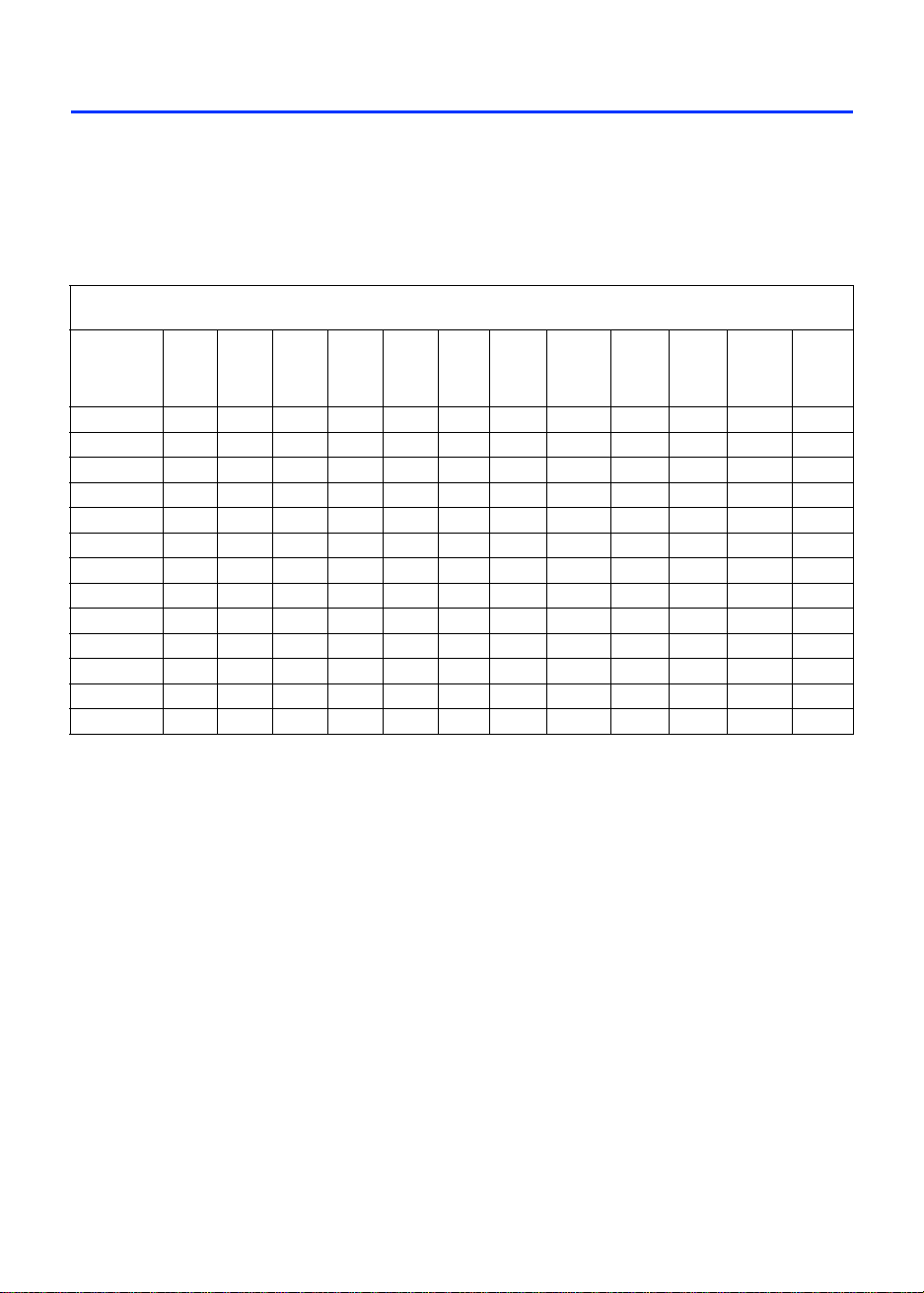
The MAX 7000 architecture includes four dedicated inputs that can
be used as general-purpose inputs or as high-speed, global control
signals (clock, clear, and two output enable signals) for each
macrocell and I/O pin. Figure1 shows the ar chite cture of EPM7032 ,
EPM7064, and EPM7096 devic es .
Figure 1. EPM7032, EPM7064 & EPM7096 Device Block Diagram
INPUT/GLCK1
INPUT/GCLRn
INPUT/OE1
INPUT/OE2
LAB A LAB B
8 to 16
I/O pins
8 to 16
I/O pins
I/O
Control
Block
I/O
Control
Block
8 to 16
8 to 16
LAB C
Macrocells
1 to 16
Macrocells
33 to 48
16
8 to 16
16
8 to 16
LAB D
8 to 16
8 to 16
I/O
Control
Block
I/O
Control
Block
8 to 16
I/O pins
8 to 16
I/O pins
36
36
PIA
36
36
16
8 to 16
16
8 to 16
Macrocells
17 to 32
Macrocells
49 to 64
Altera Corporation 7
Page 8
MAX 7000 Programm ab le Logic D evi ce F ami ly Data Sheet
I
s
s
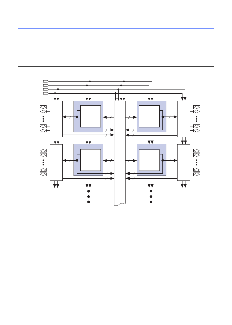
Figure2 shows the architecture of MAX 7000E and MAX 7000S devices.
Figure 2. MAX 7000E & MAX 7000S Device Block Diagram
INPUT/GCLK1
NPUT/OE2/GCLK2
INPUT/OE1
INPUT/GCLRn
6 Output Enables
6 Output Enables
Macrocells
17 to 32
Macrocells
49 to 64
LAB B
LAB D
6 to16
6 to16
6 to16
6 to16
I/O
Control
Block
I/O
Control
Block
6 to 16 I/O Pin
6
6 to 16 I/O Pin
6
LAB A
6 to16
6 to16
6 to 16 I/O Pins
6 to 16 I/O Pins
I/O
Control
Block
I/O
Control
Block
6
6 to16
6 to16
6
LAB C
Macrocells
1 to 16
Macrocells
33 to 48
36 36
16
6 to16
36 36
16
6 to16
PIA
16
6 to16
16
6 to16
Logic Array Blocks
The MAX 7000 device architecture is based on the linking of highperformance, flexible, logic array modules called logic array blocks
(LABs). LABs consist of 16-macr ocell array s, as shown in Figures 1 and 2.
Multiple LABs are linked together via the programmable interconnect
array (PIA), a global bus that is fed by all dedicated inputs, I/O pins, and
macrocells.
8 Altera Corporation
Page 9
MAX 7000 Programmabl e Log i c Dev ic e Fam ily Data Sheet
-
er
S
M
x
f
er
y
a
(
)
S
Each LAB is fed by the following signals:
■ 36 signals from the PIA that are used for general logic inputs
■ Global controls that are used for secondary register functions
■ Direct input paths from I/O pins to the registers that are used
for fast setup times for MAX 7000E and MAX 7000S devices
Macrocells
The MAX 7000 macrocell ca n be individu ally configured for either
sequential or combinatorial logic operation. The macrocell consists
of three functional blocks: the logic array, the product-term select
matrix, and the programmable register. The macrocell of EPM7032,
EPM7064, and EPM7096 devic es i s s hown in Figure 3.
Figure 3. EPM7032, EPM7064 & EPM7096 Device Macrocell
Logic Arra
Product
elect
atri
rallel Logic
Expanders
from other
macrocells
Global
Clear
Clear
Select
Global
Clocks
2
VCC
Clock/
Enable
Select
Fast Input
Select
PRN
D/T Q
ENA
CLRN
Programmable
Register
Register
Bypass
From
I/O pin
To I/O
Control
Block
to PIA
36 Signals
rom PIA
16 Expander
Product
hared Logic
Expanders
ms
Altera Corporation 9
Page 10
MAX 7000 Programm ab le Logic D evi ce F ami ly Data Sheet
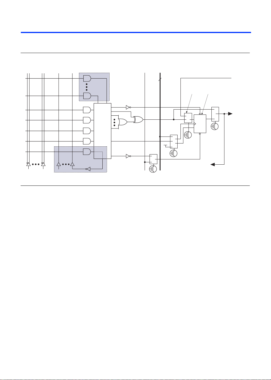
Figure4 shows a MAX 7000E and MAX 7000S device macrocell.
Figure 4. MAX 7000E & MAX 7000S Device Macrocell
Logic Array
Product-
Term
Select
Matrix
Parallel Logic
Expanders
(from other
macrocells)
Global
Clear
Clear
Select
Global
Clocks
2
VCC
Clock/
Enable
Select
Fast Input
Select
PRN
D/T Q
ENA
CLRN
Programmable
Register
Register
Bypass
from
I/O pin
to I/O
Control
Block
36 Signals
from PIA
16 Expander
Product T erms
Shared Logic
Expanders
to PIA
Combinatorial logic is implemented in the logic array, which provides
five product terms per macroce ll. The product-term select matrix allocates
these product terms for use as either primary logic inputs (to the OR and
XOR gates) to implement combinatorial functions, or as secondary inputs
to the ma crocell’s register clear, preset, cl ock, and clock enable control
functions. Two kinds of expander product terms (“expanders”) are
available to supplement macrocell logic resources:
■ Sharea ble expanders, which are inverted product terms that are fed
back into the logic array
■ Parallel expanders, which are product terms borrowed from adjacent
macrocells
The Altera developm en t sys te m aut omatically optimizes pro du ct-term
allocation according to the logic requirements of the design.
For registered functions, each macrocell flipflop can be individually
programmed to implement D, T, JK, or SR operation with prog rammable
clock control. The flipflop can be bypassed for combinatorial operation.
During design entry, the designer specifies the desired flipflop type; the
Altera development software then selects the most efficient flipflop
operation for each registered function to optimize resource utilization.
10 Altera Corporation
Page 11

MAX 7000 Programmabl e Log i c Dev ic e Fam ily Data Sheet
Each programmable regist er can be clock ed in th ree differe nt mo des:
■ By a global clock signal. This mode achieves th e fastest clock-to -
output performance.
■ By a glo b al clock signal and ena b led by an active-high clock
enable. This mode provides an enable on each flipflop while still
achieving the fast clock-to-output performance of the global
clock.
■ By an array clock implemented with a product term. In this
mode, the flipflop can be clocked by signals from buried
macrocells or I/O pins.
In EPM7032, EPM7064, and EPM7096 devices, the global clock signal
is available from a dedicated clock pin, GCLK1, as shown in Figure 1.
In MAX 70 00E a n d M A X 7000S devices, two glob al cl ock signals ar e
available. As show n in Figure 2, these global clock signals can be the
true or the complement of either of the global clock pins, GCLK1 or
GCLK2.
Each register also suppor ts asynchr onous prese t and clear functions.
As shown in Figures 3 and 4, the product -term select matrix al locates
product terms to control these operations. Although the
product-term-driven preset and clear of the register are active high,
active-low control c an be obta ined by inve rting t he signal within t he
logic array. In addition, each regist er c l ea r function can be
individually driven by the active-low dedica te d global clea r pin
(GCLRn). Upon power-up, each register in the device will be set to a
low state.
All MAX 7000E and MAX 70 00S I/O pins h ave a f a st input path to a
macrocell registe r . T his ded ica te d pat h a llows a s ig nal to by pas s t he
PIA and combinatorial logic and be driven t o an input D flipflop w ith
an extremely fast (2.5 ns) input setup time.
Expander Product Terms
Although most logic functions can be implemented with the five
product terms available in each macrocell, the more complex logic
functions require additional product terms. Another macrocell can
be used to supply the required logic resources; however, the
MAX 7000 architecture also allows both shareable and parallel
expander product terms (“expanders”) that provide additional
product terms directly to any macrocell in the same LAB. These
expanders help ensure that logic is synthesized with the fewest
possible logic resources to obtain the fastest possible speed.
Altera Corporation 11
Page 12
MAX 7000 Programm ab le Logic D evi ce F ami ly Data Sheet
m
m
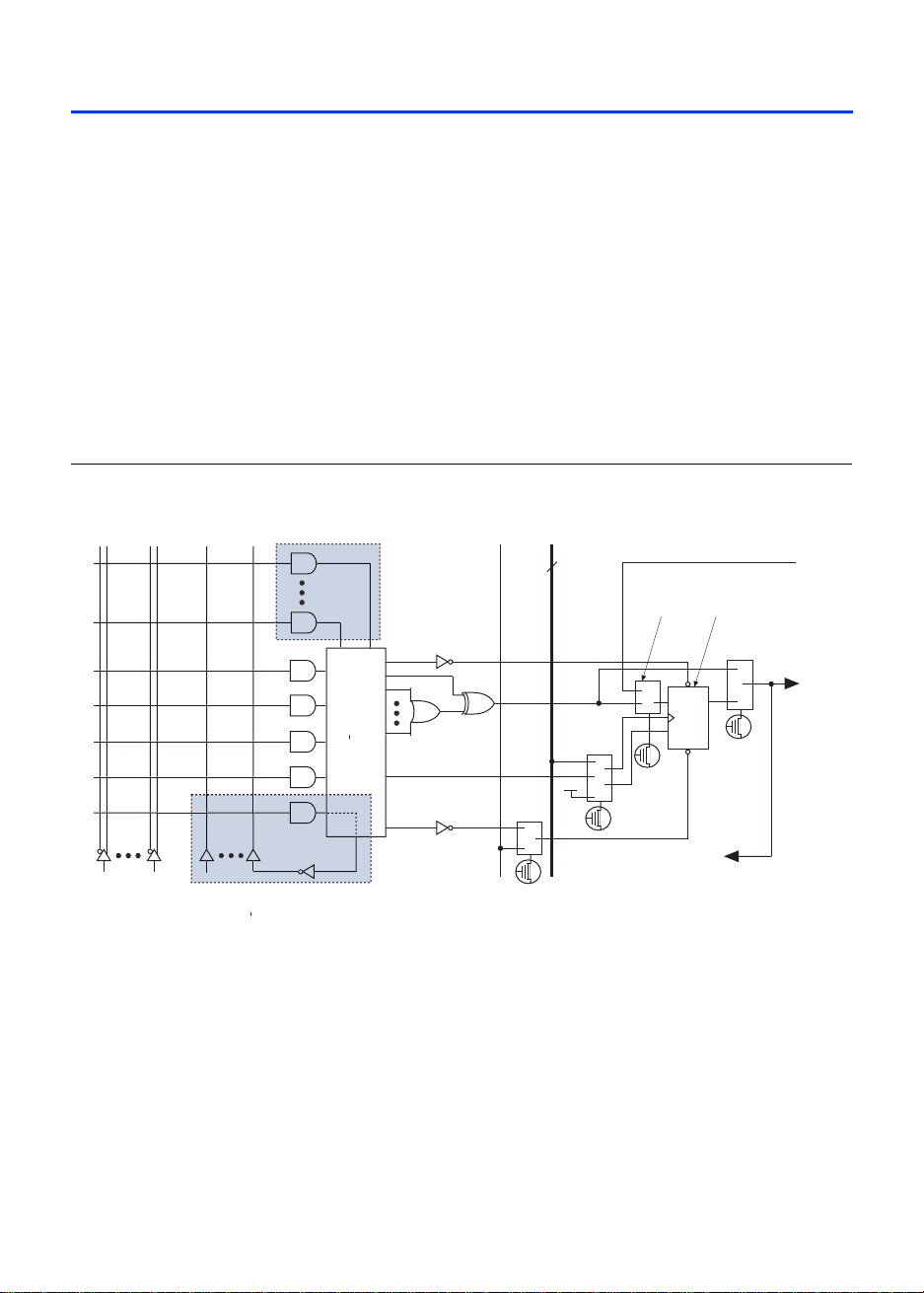
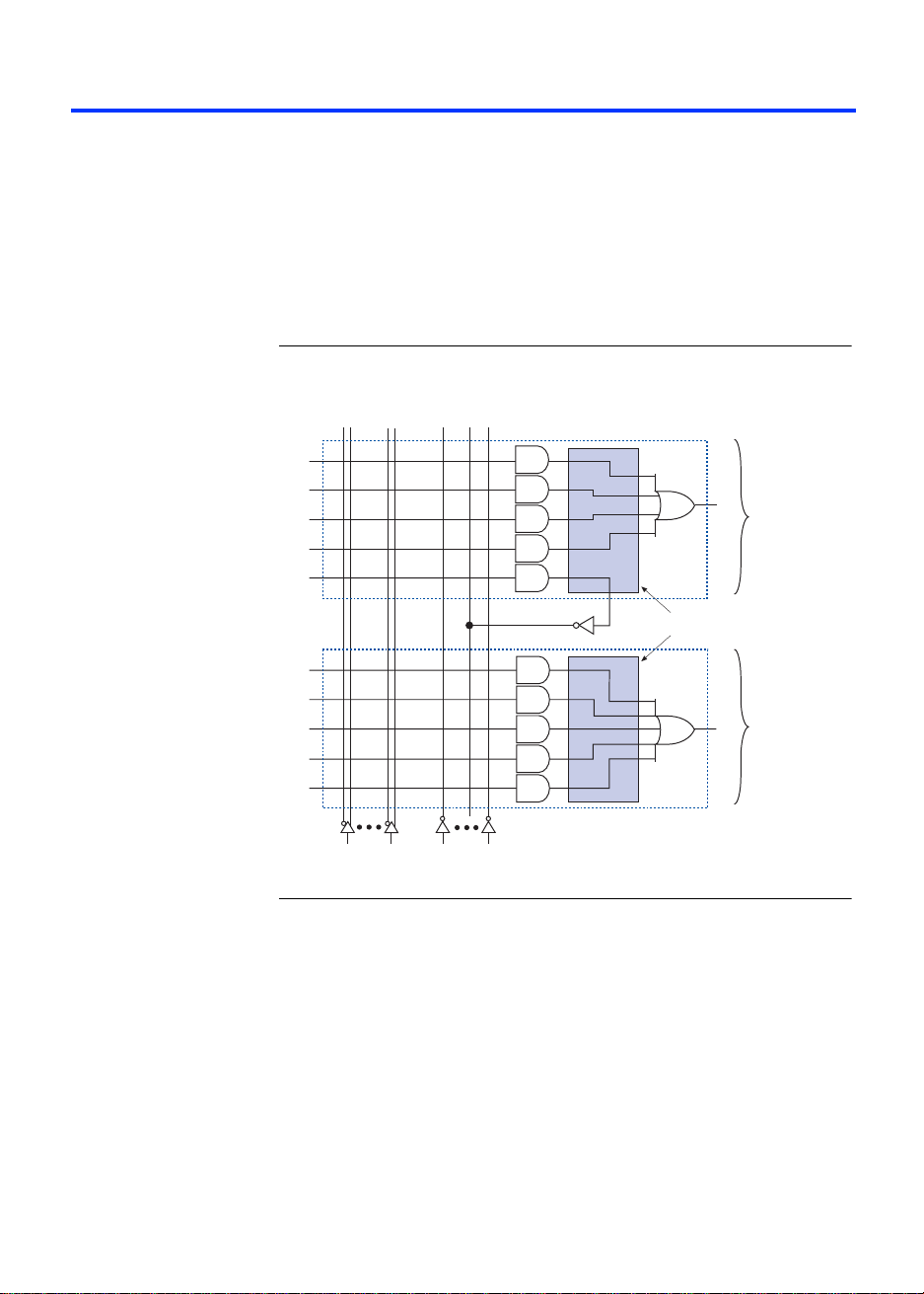
Shareable Expanders
Each LAB has 16 shareable expanders that can be viewed as a pool of
uncommitted single product terms (one from each macrocell) with
inverted outputs that feed back into the logic array. Each shareable
expander can be used and shared by any or all macrocells in the LAB to
build complex logic functions. A small delay (t
shareable expanders are used. Figure 5 shows how shareable exp an de r s
can feed multiple macrocells.
Figure 5. Shareable Expanders
Shareable expanders can be shared by any or all macrocells in an LAB.
) is incurred when
SEXP
Product-Term Select Matrix
Macrocell
Product-Ter
Logic
Macrocell
Product-Ter
Logic
36 Signals
from PIA
Parallel Expanders
16 Shared
Expanders
Parallel expanders are unused product terms that can be allocated to a
neighboring macrocell to implement fast, complex logic functions.
Parallel expanders allow up to 20 product terms to directly feed the
macrocell OR logic, with five product te rms provided by the macrocell and
15 parallel expanders provided by neighboring macrocells in the LAB.
12 Altera Corporation
Page 13
MAX 7000 Programmabl e Log i c Dev ic e Family Data Sheet
From
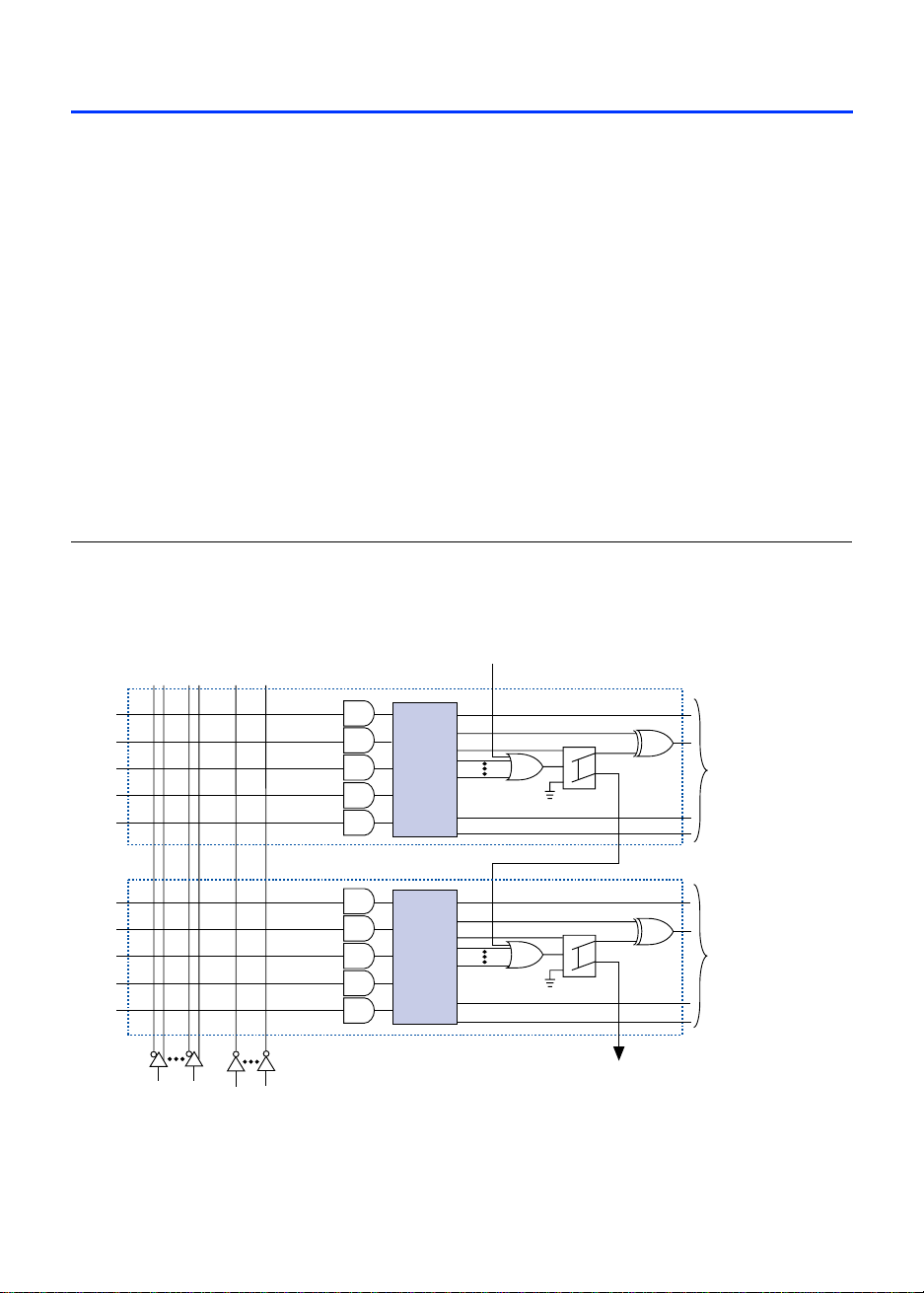
The compile r can allocate up t o three sets of up to f iv e p ar al l el ex pa nd ers
automatically to the macrocells that require additional product terms.
Each set of five parallel expanders incurs a small, incremental timing
delay (t
). For example, if a macrocell requires 14 product terms, the
PEXP
Compiler use s the five dedicated pr oduct terms within the macroce ll a nd
allocates two se ts of parallel expande rs; the first set includ e s fiv e p rodu ct
terms and th e secon d set includ es fo ur product terms , inc reasing the to tal
delay by 2 × t
PEXP
.
Two groups of 8 macrocells within each LAB (e.g., macrocells
1 through 8 and 9 through 16) form two chains to lend or borrow parallel
expanders. A macrocell borrows parallel expanders from lowernumbered macrocells. For example, macrocell 8 can borrow parallel
expanders from macrocell 7, from macrocells 7 and 6, or from macrocells
7, 6, and 5. Within each group of 8, the lowest-numbered macrocell can
only lend parallel expanders and the highest-numbered macrocell can
only borrow them. Figure 6 shows how parallel ex pa nd er s ca n be
borrowed from a neighboring macrocell.
Figure 6. Parallel Expanders
Unused product terms in a macrocell can be allocated to a neighboring macrocell.
Previous
Macrocell
Preset
36 Signals
from PIA
16 Shared
Expanders
Product-
Term
Select
Matrix
Product-
Term
Select
Matrix
Clock
Clear
Preset
Clock
Clear
To Next
Macrocell
Macrocell
ProductTerm Logic
Macrocell
ProductTerm Logic
Altera Corporation 13
Page 14
MAX 7000 Programm ab le Logic D evi ce F ami ly Data Sheet
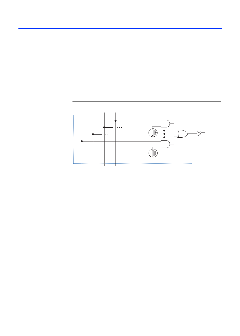
Programmable Int er co nnec t A rray
Logic is routed between LABs via the programmable interconnect array
(PIA). This global bus is a programmable path that connects any signal
source to any destination on the device. All MAX 7000 dedicated inputs,
I/O pins, and macrocell outputs feed the PIA, which makes the signals
available thro ugh out t he e ntire device. Only the sig nals required by eac h
LAB are actually routed from the PIA into the LAB. Figure 7 shows how
the PIA signals are routed into the LAB. An EEPROM cell controls one
input to a 2-input AND gate, which selects a PIA signal to drive into the
LAB.
Figure 7. PIA Ro ut ing
PIA
Signals
To LAB
While the routing dela ys of cha nne l-b ased r outi ng sche me s in ma sk ed or
FPGAs are cumulativ e, vari able, and path-d epen dent, the MAX 7000 PI A
has a fixed delay. The PIA thus eliminates skew between signals and
makes timing performance easy to predict.
I/O Control Blocks
The I/O control block allows each I/O pin to be individually configured
for input, output, or bidirectional operation. All I/O pins have a tri-state
buffer that is individually controlled by one of the global output enable
signals or directly connected to ground or V
control block for the MAX 7000 family. The I/O control block of EPM7032,
EPM7064, and EP M7096 device s has two global outp ut enable signal s that
are driven by t wo dedicate d active-low ou tput ena ble pins ( OE1 and OE2).
The I/O control block of MAX 7000E and MAX 7000S devices has six
global output enab le signa ls that are d riven by the true or complemen t of
two output enable sig na ls, a s ubse t of t he I /O pin s, o r a sub set of the I /O
macrocells.
14 Altera Corporation
. Figure 8 shows the I/O
CC
Page 15

MAX 7000 Programmabl e Log i c Dev ic e Family Data Sheet
E
M
F
Figure 8. I/O Control Block of MAX 7000 Devices
PM7032, EPM7064 & EPM7096 Devices
VCC
OE1
OE2
GND
rom Macrocell
AX 7000E & MAX 7000S Devices
To PIA
Six Global Output Enable Signals
PIA
VCC
To Other I/O Pins
From
Macrocell
Fast Input to
Macrocell
Register
To PIA
GND
Open-Drain Output (1)
Slew-Rate Control
Note:
(1) The open- d r ain o utput option is available only in MAX 700 0S d ev i c e s.
Altera Corporation 15
Page 16

MAX 7000 Programm ab le Logic D evi ce F ami ly Data Sheet
When the tri-state buffer control is connected to ground, the output is
tri-stated (high impedance) and the I/O pin can be used as a dedicated
input. When the tri-sta te buffer cont r ol is con ne cted to V
enabled.
The MAX 7000 architecture provides dual I/O feedback, in which
macrocell and pin feedbacks are independent. When an I/O pin is
configured as an input, the associated macrocell can be used for buried
logic.
, the output is
CC
In-System
Programmability (ISP)
MAX 7000S devices are in-system programmable via an
industry-standard 4-pin Joint Test Action Group (JTAG) interface (IEEE
Std. 1149.1-1990). ISP allows quick, efficient iterations during design
development and debugging cycles. The MAX 7000S architecture
internally generates the high programming voltage required to program
EEPROM cells, allowing in-syst em programming wit h only a sing le 5.0 V
power supply. Du ring in-system pr ogramming, the I /O pins are tri- stated
and pulled-up to eliminate boa rd conflicts. The pull-up value is nomi nally
50 k¾.
ISP simplifies the man ufacturing flow by allowi ng devices to be mou nted
on a printed circuit board with standard in-circuit test equipment before
they are programmed. MAX 7000S devices can be programmed by
downloading the information via in-circuit teste rs (ICT), embedde d
processors, or the Altera MasterBlaster, ByteBlasterMV, ByteBlaster,
BitBlaster download cables. (The ByteBlaster cable is obsolete and is
replaced by the ByteBlast erMV cable, which can program and config ure
2.5-V, 3 .3-V, and 5.0-V dev ices.) Pr ogramming the dev ices afte r they are
placed on the board eliminates lead damage on high-p in-cou nt pa ck ages
(e.g., QFP packages) due to device handling and allows devices to be
reprogrammed after a system has already shipped to the field. For
example, product upgrades can be performed in the field via software or
modem.
In-system programming can be accomplished with either an adaptive or
constant algorithm. An adaptive algorithm reads information from the
unit and adapts subsequent programming steps to achieve the fastest
possible programming time for that unit. Because some in-circuit testers
cannot support a n adaptive alg or ithm, Altera o ff ers d evic es te st ed w i th a
constant algorithm. Devices tested to the constant algorithm have an “F”
suffix in the ordering code.
TM
The Jam
used to program MAX 7000S devices with in-circuit testers, PCs, or
embedded processor.
16 Altera Corporation
Standard Test and Programming Lang uage (STAPL) can be
Page 17

MAX 7000 Programmabl e Log i c Dev ic e Family Data Sheet
f
Programmable Speed/Power Control
Output Configuration
For more information on using the Jam language, see Application Note 88
(Using the Jam Language for ISP & ICR via an Embedded Processor).
The ISP circuitr y in MAX 7000S devices is compa tible wit h IEEE Std. 1532
specification. The IEEE Std. 1532 is a standard developed to allow
concurrent ISP between multiple PLD vendors.
MAX 7000 devices offer a power-saving mode that supports low-power
operation across user-defined signal paths or the entire device. This
feature allows total power dissipation to be reduced by 50% or more,
because most logic a pplications require only a s mall fraction of all gates to
operate at maximum frequency.
The designer can program each individual macrocell in a MAX 7000
device for either high-speed (i.e., with the Turbo Bit
or low-power (i.e., with the Turbo Bit option turned off) operation. As a
result, speed-critical paths in the design can run at high speed, while the
remaining paths can operate a t reduced powe r. Macrocells tha t run at low
power incur a nominal timing delay adder (t
, and t
t
EN
MAX 7000 device outputs can be programmed to meet a variety of
system- level requ irements.
SEXP
, t
ACL
, and t
CPPW
parameters.
) for the t
LPA
TM
option turned on)
, t
LAC
, tIC,
LAD
MultiVolt I/O Inter fac e
MAX 7000 devices—except 44-pin devices—support the MultiVolt I/O
interface feature, which allows MAX 7000 devices to interface with
systems that have differi ng suppl y voltages . The 5.0-V devices in all
packages can be set for 3.3-V or 5.0-V I/O pin operation. These devices
have one set of VCC pins for internal operation and input buffers
(VCCINT), and another set for I/O output drivers (VCCIO).
The VCCINT pins must always be connected to a 5.0-V power supply.
With a 5.0-V V
are therefore compatible with both 3.3-V and 5.0-V input s.
The VCCIO pins can be connected to either a 3.3-V or a 5.0-V power
supply, depend ing on the outpu t requireme nts. When the VCCIO pins ar e
connected to a 5.0-V supply, the output levels are compatible with 5.0-V
systems. When V
3.3 V and is therefore compatible with 3.3-V or 5.0-V systems. Devices
operating with V
timing delay o f t
Altera Corporation 17
level, input voltage t hresholds ar e at TTL level s, and
CCINT
is connected to a 3.3-V supply, the output high is
CCIO
levels lower than 4.75 V incur a nominally greater
CCIO
instead of t
OD2
OD1
.
Page 18

MAX 7000 Programm ab le Logic D evi ce F ami ly Data Sheet
Open-Drain Output Option (MAX 7000S Devic es Only )
MAX 7000S devices provide an optional open-drain (functionally
equivalent to open-collector) output for each I/O pin. This open-drain
output enables the device to provide system-level control signals (e.g.,
interrupt and write enable signals) that can be asserted by any of several
devices. It can also provide an additional wired-OR plane.
By using an external 5.0-V pull-up resistor, output pins on MAX 7000S
devices can be set to meet 5.0-V CMOS input voltages. When V
3.3 V, setting the open drain option will turn off the output pull-up
transistor, allowing the external pull-up resistor to pull the output high
enough to meet 5.0-V CMOS input volt ages. Whe n V
the output drain option is not ne cessary becau se the pull-up transistor wil l
already turn off when the pin exceeds approximately 3.8 V, allowing the
external pull-up resistor to pull the output high enough to meet 5.0-V
CMOS input voltages.
Slew-Rate Control
The output buffer for each MAX 7000E and MAX 7000S I/O pin has an
adjustable output slew rate that can be configured for low-noise or highspeed performance. A faster slew rate provides high-speed transitions for
high-performance systems. However, these fast transitions may introduce
noise transients into the system. A slow slew rate reduces system noise,
but adds a nominal delay of 4 to 5 ns. In MAX 7000E devices, when the
Turbo Bit is turne d off, the sle w rate is set for low noi se perf orm a nce . F or
MAX 7000S devices, each I/O pin has an individual EEPROM bit that
controls the slew rate, allowing designers to specify the slew rate on a
pin-by-pin basis.
is 5.0 V , setting
CCIO
CCIO
is
Programming with External Hardware
f
f
18 Altera Corporation
MAX 7000 devices can be programme d on Windows-based PCs wi th the
Altera Logic Programmer card, the Master Programming Unit (MPU),
and the appropriate device adapter. The MPU performs a continuity
check to ensure adequate electrical contact between the adapter and the
device.
For more information, see the Altera Programming Hardware Data Sheet.
The Altera development system can use text- or waveform-format test
vectors created with the Text Editor or Waveform Editor to test the
programmed device. For added design verification, designers ca n
perform functional testing to compare the functional behavior of a
MAX 7000 device with the results of simulation. Moreover, Data I/O, BP
Microsystems, and other programming hardware manufacturers also
provide programming support for Altera devices.
For more information, see the Programming Hardware Manufacturers.
Page 19
MAX 7000 Programmabl e Log i c Dev ic e Family Data Sheet
IEEE Std.
1149.1 (JTAG)
Boundary-Scan
Support
MAX 7000 devices support JTAG BST circuitry as specified by IEEE Std.
1149.1-1990. Table 6 describes the JTAG instructions supported by the
MAX 7000 family. The pin-ou t tables (see the Alter a web site
(http://www.altera.com) or the Altera Digital Library for pin-out
information) show the location of the JTAG control pins for each device.
If the JTAG interface is not required, the JTAG pins are available as user
I/O pins.
Table 6. MAX 7000 JTAG Instructions
JTAG Instruction Devices Description
SAMPLE/PRELOAD EPM7128S
EPM7160S
EPM7192S
EPM7256S
EXTEST EPM7128S
EPM7160S
EPM7192S
EPM7256S
BYPASS EPM7032S
EPM7064S
EPM7128S
EPM7160S
EPM7192S
EPM7256S
IDCODE EPM7032S
EPM7064S
EPM7128S
EPM7160S
EPM7192S
EPM7256S
ISP Instructions EPM7032S
EPM7064S
EPM7128S
EPM7160S
EPM7192S
EPM7256S
Allows a snapshot of signals at the dev ic e pins to be capt ured and
examined during normal dev ic e operation, and permits an initial dat a
pattern output at the device pins.
Allows the external circuit ry and board-level interconnection s to be
tested by forcing a test pattern at the ou tpu t pin s and capturing test
results at the input pins.
Places the 1-bit bypass register bet w een th e TDI and TDO pins, which
allows the BST data to pass synchronously through a selected device
to adjacent devices durin g norm al dev ic e operation.
Selects the IDCODE regist er and places it between TDI and TDO,
allowing the IDCODE to be ser ially shift ed out of TDO.
These instructions are us ed wh en programming MAX 7000S devices
via the JTAG ports with the Maste rBlas t er, ByteBlasterMV, BitBlaster
download cable, or using a Jam File (.jam), Jam Byte-Code file (.jbc),
or Serial Vector Format file (.svf) v ia an em bedded processor or test
equipment.
Altera Corporation 19
Page 20

MAX 7000 Programm ab le Logic D evi ce F ami ly Data Sheet
The instruction register length of MAX 7000S devices is 10 bits. Tables 7
and 8 show the boundary-scan register length and device IDCODE
information for MAX 7000S devices.
Table 7. MAX 7000S Boundary-Scan Register Length
Device Boundary-Scan Register Length
EPM7032S 1 (1)
EPM7064S 1 (1)
EPM7128S 288
EPM7160S 312
EPM7192S 360
EPM7256S 480
Note:
(1) This device does not support JTAG boundary-scan testing. Selecting either the
EXTEST or SAMPLE/PRELOAD instruction will select the one-bit bypass register.
Table 8. 32-Bit MAX 7000 Device ID CO DE Note (1)
Device IDCODE (32 Bits)
Version
(4 Bits)
EPM7032S 0000 0111 0000 0011 0010 00001101110 1
EPM7064S 0000 0111 0000 0110 0100 00001101110 1
EPM7128S 0000 0111 0001 0010 1000 00001101110 1
EPM7160S 0000 0111 0001 0110 0000 00001101110 1
EPM7192S 0000 0111 0001 1001 0010 00001101110 1
EPM7256S 0000 0111 0010 0101 0110 00001101110 1
Notes:
(1) The most significant bit (MSB) is on the left.
(2) The least significant bit (LSB ) for all JTAG IDCODEs is 1.
20 Altera Corporation
Part Number (16 Bits) Manufacturer ’ s
Identity (11 Bits)
1 (1 Bit)
(2)
Page 21

MAX 7000 Programmabl e Log i c Dev ic e Family Data Sheet
Figure 9 shows the timing requir ements for the JTAG signals.
Figure 9. MAX 7000 JTAG Waveforms
MS
TDI
t
JCP
JCH
t
JCL
t
JPSU
t
JPH
t
CK
t
JPXZ
DO
nal
Be
red
nal
Be
iven
t
JPZX
t
JSZX
t
JSSU
t
JPCO
t
JSH
t
JSCO
t
JSXZ
Table 9 shows the JTAG timing parameters and values for
MAX 7000S devices.
Table 9. JTAG Timing Parameters & Values for MAX 7000S Devices
Symbol Parameter Min Max Unit
t
TCK clock period 100 ns
JCP
TCK clock high time 50 ns
t
JCH
t
TCK clock low time 50 ns
JCL
JTAG port setup time 20 ns
t
JPSU
t
JTAG port hold time 45 ns
JPH
JTAG port clock to output 25 ns
t
JPCO
JTAG port high impeda nc e to valid out put 25 ns
t
JPZX
t
JTAG port valid output to high im pedance 25 ns
JPXZ
Capture register setu p time 20 ns
t
JSSU
t
Capture register hold time 45 ns
JSH
t
Update register clock to outp ut 25 ns
JSCO
t
Update register high impedance to valid output 25 ns
JSZX
Update register valid out put to hig h imp edance 25 ns
t
JSXZ
Altera Corporation 21
Page 22

MAX 7000 Programm ab le Logic D evi ce F ami ly Data Sheet
VCC
f
Design Security
Generic Testing
For more information, see Application Note 39 (IEEE 1149.1 (JTAG)
Boundary-Scan Testing in Altera Devices).
All MAX 7000 devices contain a programmable security bit that controls
access to the data programmed into the device. When this bit is
programmed, a proprietary design implemented in the device cannot be
copied or retrieved. This feature provides a high level of design security
because progra mmed data w ithi n EEPRO M c ells is i nvisi ble. The securit y
bit that controls this function, as well as all other programmed data, is
reset only when the device is reprogrammed.
Each MAX 7000 device is functionally tested. Complete testing of each
programmable EEPROM bit an d all inte rna l log ic ele ments e ns ur es 10 0%
programming yield. AC test measurements are taken under conditions
equivalent to those show n in Figure 10. Test patterns can be used and then
erased during early stages of the production flow.
Figure 10. MAX 7000 AC Test Conditions
Power supply transients can affect AC
measurements. Simultaneous
transitions of m ulti pl e out put s sh ould be
avoided for accurate measurement.
Threshold tes ts must not be performed
under AC condit ions. Large-ampli tude,
fast ground- current transients normally
occur as the device outputs discharge
the load capacitances. When these
transients flow through the parasitic
inductance be tween the device grou nd
pin and the test system ground,
significant reductions in observable
noise immunity can result. Numbers in
brackets are for 2.5-V devices and
outputs. Numbers without brackets are
for 3.3-V devices and outputs.
464 Ω
[703 Ω]
Device
Output
250
[8.06 ]
KΩ
Device input
rise and fall
times < 3 ns
To Test
System
Ω
C1 (includes JIG
capacitance)
QFP Carrier & Development Socket
MAX 7000 and MAX 7000E devices in QFP packages with 100 or more
pins are shipped in special plastic carriers to protect the QFP leads. The
carrier is used with a prototype development socket and special
programming hardware available from Alter a. This carrie r technology
makes it possi ble to program , test , erase , an d reprog ram a de vice wi thout
exposing the leads to mechanical stress.
f
For detailed information and carrier dimensions , refer to the QFP Carrier
& Development Socket Data Sheet.
1 MAX 7000S device s are not shipped in carriers.
22 Altera Corporation
Page 23

MAX 7000 Programmabl e Log i c Dev ic e Family Data Sheet
Operating Conditions
Tables 10 through 15 provide information about absolute maximum
ratings, recommended operating conditions, operating conditions, and
capacitance for 5.0-V MAX 7000 de v ic es.
Table 10.MAX 7000 5.0-V Device Absolute Maximum Ratings Note (1)
Symbol Parameter Conditions Min Max Unit
V
V
I
T
T
T
OUT
Supply voltage With respect to ground (2) –2.0 7.0 V
CC
DC input voltage –2.0 7.0 V
I
DC output current, per pin –25 25 mA
Storage temperature No bias –65 150 ° C
STG
Ambient temperature Under bias –65 135 ° C
AMB
Junction temperature Ceramic packages, under bias 150 ° C
J
PQFP and RQFP packages, under bias 135 ° C
Table 11. MAX 7000 5.0-V Device Recommended Operat ing Conditions
Symbol Parameter Conditions Min Max Unit
V
V
V
V
V
T
T
t
R
t
F
Supply voltage for internal logic and
CCINT
input buffers
Supply voltage for output drivers,
CCIO
5.0-V operation
Supply voltage for output drivers,
3.3-V operation
Supply voltage during ISP (7) 4.75 5.25 V
CCISP
Input voltage –0.5 (8) V
I
Output voltage 0V
O
Ambient temperature For commercial use 0 70 ° C
A
Junction temperature For commercial use 0 90 ° C
J
Input rise time 40 ns
Input fall time 40 ns
(3), (4), (5) 4.75
(4.50)
(3), (4) 4.75
(4.50)
(3), (4), (6) 3.00
(3.00)
For industrial use –40 85 ° C
For industrial use –40 105 ° C
5.25
(5.50)
5.25
(5.50)
3.60
(3.60)
CCINT
CCIO
+ 0.5 V
V
V
V
V
Altera Corporation 23
Page 24

MAX 7000 Programm ab le Logic D evi ce F ami ly Data Sheet
Table 12. MAX 7000 5.0-V Device D C Ope r ating Conditions Note (9)
Symbol Parameter Conditions Min Max Unit
V
V
V
V
I
I
I
OZ
High-level input voltage 2.0 V
IH
Low-level input voltage –0.5 (8) 0.8 V
IL
5.0-V high-level TTL output voltage IOH = –4 mA DC, V
OH
3.3-V high-level TTL output voltage I
3.3-V high-level CMOS output
voltage
5.0-V low-level TTL output voltage IOL = 12 mA DC, V
OL
3.3-V low-level TTL output voltage I
3.3-V low-level CMOS output
voltage
Leakage current of dedicated input
= –4 mA DC, V
OH
I
= –0.1 mA DC, V
OH
= 12 mA DC, V
OL
I
= 0.1 mA DC, V
OL
VI = –0.5 to 5.5 V (11) –10 10 µA
= 4.75 V (10) 2.4 V
CCIO
= 3.00 V (10) 2.4 V
CCIO
= 3.0 V (10) V
CCIO
= 4.75 V (11) 0.45 V
CCIO
= 3.00 V (11) 0.45 V
CCIO
= 3.0 V(11) 0.2 V
CCIO
– 0.2 V
CCIO
pins
I/O pin tri-state output off-state
VI = –0.5 to 5.5 V (11), (12) –40 40 µA
current
CCINT
+ 0.5 V
Table 13. MAX 7000 5.0-V D evice Cap a citance : EPM7032, EPM7064 & EPM7096 De vices Note (13)
Symbol Parameter Conditions Min Max Unit
C
C
Input pin capacitance VIN = 0 V, f = 1.0 MHz 12 pF
IN
I/O pin capacitance V
I/O
= 0 V, f = 1.0 MHz 12 pF
OUT
Table 14. MAX 7000 5.0-V Device Cap acitance : MAX 7000E Devices Note (13)
Symbol Parameter Conditions Min Max Unit
C
C
Input pin capacitance VIN = 0 V, f = 1.0 MHz 15 pF
IN
I/O pin capacitance V
I/O
= 0 V, f = 1.0 MHz 15 pF
OUT
Table 15. MAX 7000 5.0-V Device Cap acitance : MAX 7000S Devices Note (13 )
Symbol Parameter Conditions Min Max Unit
C
C
24 Altera Corporation
Dedicated input pin capacitance VIN = 0 V, f = 1.0 MHz 10 pF
IN
I/O pin capacitance V
I/O
= 0 V, f = 1.0 MHz 10 pF
OUT
Page 25

MAX 7000 Programmabl e Log i c Dev ic e Family Data Sheet
T
O
C
Notes to tables:
(1) See the Ope rat i ng Requirements for Al t era Devices Data Sheet.
(2) Minimum DC input vol t age on I/O pins is –0. 5 V and on 4 dedic a te d in put pins is –0.3 V. During transitions, the
inputs may undershoot to –2.0 V or overshoot to 7.0 V for input currents less than 100 mA and periods shorter than
20 ns.
(3) Numbers in parentheses are for industrial-temperature-range devices.
(4) V
(5) The POR time for all 7000S devices does not exceed 300 µs. The sufficient V
(6) 3.3-V I/O operation is not available for 44-pin packages.
(7) The V
(8) During in-system pr og r amming, the minim um DC input voltage is –0.3 V.
must rise monotonically.
CC
device is fu lly initialized within the POR time after V
parameter applies only to MAX 7000S devices.
CCISP
voltage level for POR is 4.5 V. The
reaches the s ufficient POR vo ltage level.
CCINT
CCINT
(9) These values ar e s p ec ified under the M AX 7000 recomme n d ed operating conditions in Table 11 on page 23.
(10) The parameter is measured with 50% of the outputs eac h s ourcing the speci fied current. T h e I
to high-level TTL or CMOS output current.
(11) The parameter is measured with 50% of the outputs each sinking the specified current. The I
low-leve l TT L , P C I, o r CM O S output curren t .
parameter refers
OH
parameter refers to
OL
(12) When the JTAG interface is enabled in MAX 7000S devices, the input leakage current on the JTAG pins is typically
–60 µA.
(13) Capacit a n ce is measur ed at 25° C and is sample-tested only. The
OE1 pin has a maximum capacitance of 20 pF.
Figure 11 shows the typical output drive characteristics of MAX 7000
devices.
Figure 11 . Output Dri ve Charact eristics of 5.0-V MAX 7000 Devic es
150
120
90
I
ypical
O
utput
urrent (mA)
60
30
Timing Model
I
OL
Typical
V
= 5.0 V
CCIO
Room T emperature
I
OH
12345
Output
Current (mA)
VO Output Voltage (V)
MAX 7000 devic e timing can be analyz ed with the Alte ra software , with a
variety of popular industr y-s tandard EDA simulators and timing
150
120
90
I
O
60
30
12345
I
OL
V
= 3.3 V
CCIO
Room T emperature
I
OH
3.3
VO Output Voltage (V)
analyzers, or with the timing model shown in Figure 12. MAX 7000
devices have fixed interna l del ays that enable the designer to de te rmine
the worst-case timing of any design. The Alte ra soft ware pr ovides ti ming
Altera Corporation 25
simulation, point-to-point delay prediction, and detailed timing analysis
for a device-wide performance evaluation.
Page 26

MAX 7000 Programm ab le Logic D evi ce F ami ly Data Sheet
Figure 12. MAX 7000 Timing Model
Internal Output
Enable Delay
t
(1)
IOE
Input
Delay
t
IN
PIA
Delay
t
PIA
Global Control
Delay
t
GLOB
Logic Array
Delay
t
LAD
Register
Control Delay
t
LAC
t
IC
t
EN
Shared
Expander Delay
t
SEXP
Expander Delay
Notes:
(1) Only available in MAX 7000E an d MA X 7000S devices.
(2) Not available in 44-pin devices.
The timing characteristics of any signal path can be derived from the
timing model and parameters of a particular device. External timing
parameters, which represent pin-to-pin timing delays, can be calculated
as the sum of internal parameters. Figure 13 shows the internal timing
relationship of internal and external delay parameters.
Parallel
t
PEXP
Fast
Input Delay
t
FIN
(1)
Register
Delay
t
SU
t
H
t
PRE
t
CLR
t
RD
t
COMB
t
FSU
t
FH
Output
Delay
t
OD1
t
OD2
t
OD3
t
XZ
t
X1
Z
t
ZX2
t
ZX3
(2)
(2)
(1)
I/O
Delay
t
IO
f
For more infomration, see Application Note 94 (Understanding MAX 7000
Timing).
26 Altera Corporation
Page 27

Figure 13 . Switching Waveforms
MAX 7000 Programmabl e Log i c Dev ic e Family Data Sheet
tR & tF < 3 ns.
Inputs are driven at 3 V
for a logic high and 0 V
for a logic low. A ll timing
characteristics are
measured at 1.5 V.
Input Pin
I/O Pin
PIA Delay
Shared Expander
Parallel Expander
Delay
Logic Array
Input
Delay
Logic Array
Output
Output Pin
Global
Clock Pin
Global Clock
at Register
Data or Enable
(Logic Array Output)
Combinatorial Mode
t
IN
t
IO
Global Clock Mode
t
IN
tSUt
t
CH
t
GLOB
H
t
R
t
PIA
t
SEXP
t
, t
LAC
LAD
t
PEXP
t
COMB
t
OD
t
CL
t
F
Array Clock Mode
t
F
t
, t
CLR
PRE
t
PIA
t
OD
Input or I/O Pin
Clock into PIA
Clock into
Logic Array
Clock at
Register
Data from
Logic Array
Register to PIA
to Logic Array
Register Output
to Pin
t
R
t
ACH
t
IN
t
IO
t
PIA
t
ACL
t
IC
t
t
SU
H
t
RD
t
PIA
t
OD
Altera Corporation 27
Page 28

MAX 7000 Programm ab le Logic D evi ce F ami ly Data Sheet
Tables 16 through 23 show the MAX 7000 and MAX 7000E AC operating
conditions.
Table 16. MAX 7000 & MAX 7000E External Timing Parameters Note (1)
Symbol Parameter Condit i ons -6 Speed Grade -7 Speed Grade Uni t
Min Max Min Max
t
PD1
t
PD2
t
SU
t
H
t
FSU
t
FH
t
CO1
t
CH
t
CL
t
ASU
t
AH
t
ACO1
t
ACH
t
ACL
t
CPPW
t
ODH
t
CNT
f
CNT
t
ACNT
f
ACNT
f
MAX
Input to non-registered output C1 = 35 pF 6.0 7.5 ns
I/O input to non-registered output C1 = 35 pF 6.0 7.5 ns
Global clock setup time 5.0 6.0 ns
Global clock hold time 0.0 0.0 ns
Global clock setup time of fast input (2) 2.5 3.0 ns
Global clock hold time of fast input (2) 0.5 0.5 ns
Global clock to output delay C1 = 35 pF 4.0 4.5 ns
Global clock high time 2.5 3.0 ns
Global clock low time 2.5 3.0 ns
Array clock setup time 2.5 3.0 ns
Array clock hold time 2.0 2.0 ns
Array clock to output delay C1 = 35 pF 6.5 7.5 ns
Array clock high time 3.0 3.0 ns
Array clock low time 3.0 3.0 ns
Minimum pulse width for clear and
(3) 3.0 3.0 ns
preset
Output data hold time after clock C1 = 35 pF (4) 1.0 1.0 ns
Minimum global clock period 6.6 8.0 ns
Maximum internal global clock
(5) 151.5 125.0 MHz
frequency
Minimum array clock period 6.6 8.0 ns
Maximum internal array clock
(5) 151.5 125.0 MHz
frequency
Maximum clock frequency (6) 200 166.7 MHz
28 Altera Corporation
Page 29

MAX 7000 Programmabl e Log i c Dev ic e Family Data Sheet
Table 17.MAX 7000 & MAX 7000E Internal Timing Parameters Note (1)
Symbol Parameter Conditions Speed Grade -6 Speed Grade -7 Unit
Min Max Min Max
t
IN
t
IO
t
FIN
t
SEXP
t
PEXP
t
LAD
t
LAC
t
IOE
t
OD1
t
OD2
t
OD3
t
ZX1
t
ZX2
t
ZX3
t
XZ
t
SU
t
H
t
FSU
t
FH
t
RD
t
COMB
t
IC
t
EN
t
GLOB
t
PRE
t
CLR
t
PIA
t
LPA
Input pad and buffer delay 0.4 0.5 ns
I/O input pad and buffer delay 0.4 0.5 ns
Fast input delay (2) 0.8 1.0 ns
Shared expander delay 3.5 4.0 ns
Parallel expander delay 0.8 0.8 ns
Logic array delay 2.0 3.0 ns
Logic control array delay 2.0 3.0 ns
Internal output enable delay (2) 2.0 ns
Output buffer and pad delay
Slow slew rate = off, V
CCIO
Output buffer and pad delay
Slow slew rate = off, V
CCIO
Output buffer and pad delay
= 5.0 V
= 3.3 V
C1 = 35 pF 2.0 2.0 ns
C1 = 35 pF (7) 2.5 2.5 ns
C1 = 35 pF (2) 7.0 7.0 ns
Slow slew rate = on,
= 5.0 V or 3.3 V
V
CCIO
Output buffer enable delay
Slow slew rate = off, V
CCIO
Output buffer enable delay
Slow slew rate = off, V
CCIO
Output buffer enable delay
= 5.0 V
= 3.3 V
C1 = 35 pF 4.0 4.0 ns
C1 = 35 pF (7) 4.5 4.5 ns
C1 = 35 pF (2) 9.0 9.0 ns
Slow slew rate = on
= 5.0 V or 3.3 V
V
CCIO
Output buffer disable delay C1 = 5 pF 4.0 4.0 ns
Register setup time 3.0 3.0 ns
Register hold time 1.5 2.0 ns
Register setup time of fast input (2) 2.5 3.0 ns
Register hold time of fast input (2) 0.5 0.5 ns
Register delay 0.8 1.0 ns
Combinatorial delay 0.8 1.0 ns
Array clock delay 2.5 3.0 ns
Register enable time 2.0 3.0 ns
Global control delay 0.8 1.0 ns
Register preset time 2.0 2.0 ns
Register clear time 2.0 2.0 ns
PIA delay 0.8 1.0 ns
Low-power adder (8) 10.0 10.0 ns
Altera Corporation 29
Page 30

MAX 7000 Programm ab le Logic D evi ce F ami ly Data Sheet
Table 18. MAX 7000 & MAX 7000E External Timing Parameters Note (1)
Symbol Parameter Conditions Speed Grade Unit
MAX 7000E (-10P) MAX 7000 (-10)
MAX 7000E (-10 )
Min Max Min Max
t
PD1
t
PD2
t
SU
t
H
t
FSU
t
FH
t
CO1
t
CH
t
CL
t
ASU
t
AH
t
ACO1
t
ACH
t
ACL
t
CPPW
t
ODH
t
CNT
f
CNT
t
ACNT
f
ACNT
f
MAX
Input to non-registered output C1 = 35 pF 10.0 10.0 ns
I/O input to non-registered output C1 = 35 pF 10.0 10.0 ns
Global clock setup time 7.0 8.0 ns
Global clock hold time 0.0 0.0 ns
Global clock setup time of fast input (2) 3.0 3.0 ns
Global clock hold time of fast input (2) 0.5 0.5 ns
Global clock to output delay C1 = 35 pF 5.0 5 ns
Global clock high time 4.0 4.0 ns
Global clock low time 4.0 4.0 ns
Array clock setup time 2.0 3.0 ns
Array clock hold time 3.0 3.0 ns
Array clock to output delay C1 = 35 pF 10.0 10.0 ns
Array clock high time 4.0 4.0 ns
Array clock low time 4.0 4.0 ns
Minimum pulse width for clear and
(3) 4.0 4.0 ns
preset
Output data hold time after clock C1 = 35 pF (4) 1.0 1.0 ns
Minimum global clock period 10.0 10.0 ns
Maximum internal global clock
(5) 100.0 100.0 MHz
frequency
Minimum array clock period 10.0 10.0 ns
Maximum internal array clock
(5) 100.0 100.0 MHz
frequency
Maximum clock frequency (6) 125.0 125.0 MHz
30 Altera Corporation
Page 31

MAX 7000 Programmabl e Log i c Dev ic e Family Data Sheet
Table 19.MAX 7000 & MAX 7000E Internal Timing Parameters Note (1)
Symbol Parameter Conditions Speed Grade Unit
MAX 7000E (-10P) MAX 7000 (-10)
MAX 7000 E (-10)
Min Max Min Max
t
IN
t
IO
t
FIN
t
SEXP
t
PEXP
t
LAD
t
LAC
t
IOE
t
OD1
t
OD2
t
OD3
t
ZX1
t
ZX2
t
ZX3
t
XZ
t
SU
t
H
t
FSU
t
FH
t
RD
t
COMB
t
IC
t
EN
t
GLOB
t
PRE
t
CLR
t
PIA
t
LPA
Altera Corporation 31
Input pad and buffer delay 0.5 1.0 ns
I/O input pad and buffer delay 0.5 1.0 ns
Fast input delay (2) 1.0 1.0 ns
Shared expander delay 5.0 5.0 ns
Parallel expander delay 0.8 0.8 ns
Logic array delay 5.0 5.0 ns
Logic control array delay 5.0 5.0 ns
Internal output enable delay (2) 2.0 2.0 ns
Output buffer and pad delay
C1 = 35 pF 1.5 2.0 ns
Slow slew rate = off
= 5.0 V
V
CCIO
Output buffer and pad delay
C1 = 35 pF (7) 2.0 2.5 ns
Slow slew rate = off
= 3.3 V
V
CCIO
Output buffer and pad delay
C1 = 35 pF (2) 5.5 6.0 ns
Slow slew rate = on
= 5.0 V or 3.3 V
V
CCIO
Output buffer enable delay
C1 = 35 pF 5.0 5.0 ns
Slow slew rate = off
= 5.0 V
V
CCIO
Output buffer enable delay
C1 = 35 pF (7) 5.5 5.5 ns
Slow slew rate = off
= 3.3 V
V
CCIO
Output buffer enable delay
C1 = 35 pF (2) 9.0 9.0 ns
Slow slew rate = on
= 5.0 V or 3.3 V
V
CCIO
Output buffer disable delay C1 = 5 pF 5.0 5.0 ns
Register setup time 2.0 3.0 ns
Register hold time 3.0 3.0 ns
Register setup time of fast input (2) 3.0 3.0 ns
Register hold time of fast input (2) 0.5 0.5 ns
Register delay 2.0 1.0 ns
Combinatorial delay 2.0 1.0 ns
Array clock delay 5.0 5.0 ns
Register enable time 5.0 5.0 ns
Global control delay 1.0 1.0 ns
Register preset time 3.0 3.0 ns
Register clear time 3.0 3.0 ns
PIA delay 1.0 1.0 ns
Low-power adder (8) 11.0 11.0 ns
Page 32

MAX 7000 Programm ab le Logic D evi ce F ami ly Data Sheet
Table 20. MAX 7000 & MAX 7000E External Timing Parameters Note (1)
Symbol Parameter Condit i ons Speed Gr ade Unit
MAX 7000E (-1 2P ) MAX 7000 (-12)
MAX 7000 E (-12)
Min Max Min Max
t
PD1
t
PD2
t
SU
t
H
t
FSU
t
FH
t
CO1
t
CH
t
CL
t
ASU
t
AH
t
ACO1
t
ACH
t
ACL
t
CPPW
t
ODH
t
CNT
f
CNT
t
ACNT
f
ACNT
f
MAX
Input to non-registered output C1 = 35 pF 12.0 12.0 ns
I/O input to non-registered output C1 = 35 pF 12.0 12.0 ns
Global clock setup time 7.0 10.0 ns
Global clock hold time 0.0 0.0 ns
Global clock setup time of fast input (2) 3.0 3.0 ns
Global clock hold time of fast input (2) 0.0 0.0 ns
Global clock to output delay C1 = 35 pF 6.0 6.0 ns
Global clock high time 4.0 4.0 ns
Global clock low time 4.0 4.0 ns
Array clock setup time 3.0 4.0 ns
Array clock hold time 4.0 4.0 ns
Array clock to output delay C1 = 35 pF 12.0 12.0 ns
Array clock high time 5.0 5.0 ns
Array clock low time 5.0 5.0 ns
Minimum pulse width for clear and
(3) 5.0 5.0 ns
preset
Output data hold time after clock C1 = 35 pF (4) 1.0 1.0 ns
Minimum global clock period 11.0 11.0 ns
Maximum internal global clock
(5) 90.9 90.9 MHz
frequency
Minimum array clock period 11.0 11.0 ns
Maximum internal array clock
(5) 90.9 90.9 MHz
frequency
Maximum clock frequency (6) 125.0 125.0 MHz
32 Altera Corporation
Page 33

MAX 7000 Programmabl e Log i c Dev ic e Family Data Sheet
Table 21.MAX 7000 & MAX 7000E Internal Timing Parameters Note (1)
Symbol Parameter Conditions Speed Grade Unit
MAX 7000E (-12P) MAX 7000 (-12)
MAX 7000E (-12)
Min Max Min Max
t
IN
t
IO
t
FIN
t
SEXP
t
PEXP
t
LAD
t
LAC
t
IOE
t
OD1
t
OD2
t
OD3
t
ZX1
t
ZX2
t
ZX3
t
XZ
t
SU
t
H
t
FSU
t
FH
t
RD
t
COMB
t
IC
t
EN
t
GLOB
t
PRE
t
CLR
t
PIA
t
LPA
Altera Corporation 33
Input pad and buffer delay 1.0 2.0 ns
I/O input pad and buffer delay 1.0 2.0 ns
Fast input delay (2) 1.0 1.0 ns
Shared expander delay 7.0 7.0 ns
Parallel expander delay 1.0 1.0 ns
Logic array delay 7.0 5.0 ns
Logic control array delay 5.0 5.0 ns
Internal output enable delay (2) 2.0 2.0 ns
Output buffer and pad delay
C1 = 35 pF 1.0 3.0 ns
Slow slew rate = off
= 5.0 V
V
CCIO
Output buffer and pad delay
C1 = 35 pF (7) 2.0 4.0 ns
Slow slew rate = off
= 3.3 V
V
CCIO
Output buffer and pad delay
C1 = 35 pF (2) 5.0 7.0 ns
Slow slew rate = on
= 5.0 V or 3.3 V
V
CCIO
Output buffer enable delay
C1 = 35 pF 6.0 6.0 ns
Slow slew rate = off
= 5.0 V
V
CCIO
Output buffer enable delay
C1 = 35 pF (7) 7.0 7.0 ns
Slow slew rate = off
= 3.3 V
V
CCIO
Output buffer enable delay
C1 = 35 pF (2) 10.0 10.0 ns
Slow slew rate = on
= 5.0 V or 3.3 V
V
CCIO
Output buffer disable delay C1 = 5 pF 6.0 6.0 ns
Register setup time 1.0 4.0 ns
Register hold time 6.0 4.0 ns
Register setup time of fast input (2) 4.0 2.0 ns
Register hold time of fast input (2) 0.0 2.0 ns
Register delay 2.0 1.0 ns
Combinatorial delay 2.0 1.0 ns
Array clock delay 5.0 5.0 ns
Register enable time 7.0 5.0 ns
Global control delay 2.0 0.0 ns
Register preset time 4.0 3.0 ns
Register clear time 4.0 3.0 ns
PIA delay 1.0 1.0 ns
Low-power adder (8) 12.0 12.0 ns
Page 34

MAX 7000 Programm ab le Logic D evi ce F ami ly Data Sheet
Table 22. MAX 7000 & MAX 7000E External Timing Parameters Note (1)
Symbol Parameter Conditions Speed Grade Unit
-15 -15T -20
Min Max Min Max Min Max
t
PD1
t
PD2
t
SU
t
H
t
FSU
t
FH
t
CO1
t
CH
t
CL
t
ASU
t
AH
t
ACO1
t
ACH
t
ACL
t
CPPW
t
ODH
t
CNT
f
CNT
t
ACNT
f
ACNT
f
MAX
Input to non-registered output C1 = 35 pF 15.0 15.0 20.0 ns
I/O input to non-registered
C1 = 35 pF 15.0 15.0 20.0 n s
output
Global clock setup time 11.0 11.0 12.0 ns
Global clock hold time 0.0 0.0 0.0 ns
Global clock setup time of fast
(2) 3.0 – 5.0 ns
input
Global clock hold time of fast
(2) 0.0 – 0.0 ns
input
Global clock to output delay C1 = 35 pF 8.0 8.0 12.0 ns
Global clock high time 5.0 6.0 6.0 ns
Global clock low time 5.0 6.0 6.0 ns
Array clock setup time 4.0 4.0 5.0 ns
Array clock hold time 4.0 4.0 5.0 ns
Array clock to output delay C1 = 35 pF 15.0 15.0 20.0 ns
Array clock high time 6.0 6.5 8.0 ns
Array clock low time 6.0 6.5 8.0 ns
Minimum pulse width for clear
(3) 6.0 6.5 8.0 ns
and preset
Output data hold time after
C1 = 35 pF (4) 1.0 1.0 1.0 ns
clock
Minimum global clock period 13.0 13.0 16.0 ns
Maximum internal global clock
(5) 76.9 76.9 62.5 MHz
frequency
Minimum array clock period 13.0 13.0 16.0 ns
Maximum internal array clock
(5) 76.9 76.9 62.5 MHz
frequency
Maximum clock frequency (6) 100 83.3 83.3 M Hz
34 Altera Corporation
Page 35

MAX 7000 Programmabl e Log i c Dev ic e Family Data Sheet
Table 23.MAX 7000 & MAX 7000E Internal Timing Parameters Note (1)
Symbol Parameter Conditions Speed Grade Unit
-15 -15T -20
Min Max Min Max Min Max
t
IN
t
IO
t
FIN
t
SEXP
t
PEXP
t
LAD
t
LAC
t
IOE
t
OD1
t
OD2
t
OD3
t
ZX1
t
ZX2
t
ZX3
t
XZ
t
SU
t
H
t
FSU
t
FH
t
RD
t
COMB
t
IC
t
EN
t
GLOB
t
PRE
t
CLR
t
PIA
t
LPA
Input pad and buffer delay 2.0 2.0 3.0 ns
I/O input pad and buffer delay 2.0 2.0 3.0 ns
Fast input delay (2) 2.0 – 4.0 ns
Shared expander delay 8.0 10.0 9.0 ns
Parallel expander delay 1.0 1.0 2.0 ns
Logic array delay 6.0 6.0 8.0 ns
Logic control array delay 6.0 6.0 8.0 ns
Internal output enable delay (2) 3.0 – 4.0 ns
Output buffer and pad delay
C1 = 35 pF 4.0 4.0 5.0 ns
Slow slew rate = off
= 5.0 V
V
CCIO
Output buffer and pad delay
C1 = 35 pF (7) 5.0 – 6.0 ns
Slow slew rate = off
= 3.3 V
V
CCIO
Output buffer and pad delay
C1 = 35 pF (2) 8.0 – 9.0 ns
Slow slew rate = on
= 5.0 V or 3.3 V
V
CCIO
Output buffer enable delay
C1 = 35 pF 6.0 6.0 10.0 ns
Slow slew rate = off
V
= 5.0 V
CCIO
Output buffer enable delay
C1 = 35 pF (7) 7.0 – 11.0 ns
Slow slew rate = off
V
= 3.3 V
CCIO
Output buffer enable delay
C1 = 35 pF (2) 10.0 – 14.0 ns
Slow slew rate = on
V
= 5.0 V or 3.3 V
CCIO
Output buffer disable delay C1 = 5 pF 6.0 6.0 10.0 ns
Register setup time 4.0 4.0 4.0 ns
Register hold time 4.0 4.0 5.0 ns
Register setup time of fast input (2) 2.0 – 4.0 ns
Register hold time of fast input (2) 2.0 – 3.0 ns
Register delay 1.0 1.0 1.0 ns
Combinatorial delay 1.0 1.0 1.0 ns
Array clock delay 6.0 6.0 8.0 ns
Register enable time 6.0 6.0 8.0 ns
Global control delay 1.0 1.0 3.0 ns
Register preset time 4.0 4.0 4.0 ns
Register clear time 4.0 4.0 4.0 ns
PIA delay 2.0 2.0 3.0 ns
Low-power adder (8) 13.0 15.0 15.0 ns
Altera Corporation 35
Page 36

MAX 7000 Programm ab le Logic D evi ce F ami ly Data Sheet
Notes to tables:
(1) These values are specified under the recommended operating conditions shown in Table 11. See Figure 13 for more
information on switching waveforms.
(2) This parameter applies to MAX 7000E devices only.
(3) This minimum pulse width for p reset and cl ear applies fo r both global cle ar and arra y controls. The t
must be added to this minimum width if the clear or reset signal incorporates the t
path.
parameter into the signal
LAD
parameter
LPA
(4) This par a meter is a guid eline that is s a mple-teste d o nly and is based on extensiv e device ch ar a c t er ization. T hi s
parameter applies for both global and array clocking.
(5) These paramete rs are measu r ed with a 16-bit loadable, enabled, up/down coun t er prog r ammed into each LAB.
(6) The f
(7) Operating conditions: V
(8) The t
running in th e low-power mo d e.
values repres en t th e highest frequ en c y for pipelined da t a.
MAX
parameter must be added to the t
LPA
= 3.3 V ± 10% for commercial and industrial use.
CCIO
LAD
, t
, tIC, tEN, t
LAC
SEXP
, t
ACL
, and t
parameters for macrocells
CPPW
Tables 24 and 25 show the EPM7032S AC oper ati ng condit ions .
Table 24.EPM7032S External Timing Parameters (Part 1 of 2) Note (1)
Symbol Parameter Condi tions Speed Grade Unit
-5 -6 -7 -10
Min Max Min Max Min Max Min Max
t
PD1
t
PD2
t
SU
t
H
t
FSU
t
FH
t
CO1
t
CH
t
CL
t
ASU
t
AH
t
ACO1
t
ACH
t
ACL
t
CPPW
t
ODH
t
CNT
f
CNT
t
ACNT
Input to non-registered output C1 = 35 pF 5.0 6.0 7.5 10.0 ns
I/O input to non-registered
C1 = 35 pF 5.0 6.0 7.5 10.0 ns
output
Global clock setup time 2.9 4.0 5.0 7.0 ns
Global clock hold time 0.0 0.0 0.0 0.0 ns
Global clock setup time of fast
2.5 2.5 2.5 3.0 ns
input
Global clock hold time of fast
0.0 0.0 0.0 0.5 ns
input
Global clock to output delay C1 = 35 pF 3.2 3.5 4.3 5.0 ns
Global clock high time 2.0 2.5 3.0 4.0 ns
Global clock low time 2.0 2. 5 3.0 4.0 ns
Array clock setup time 0.7 0.9 1.1 2.0 ns
Array clock hold time 1.8 2.1 2.7 3.0 ns
Array clock to output delay C1 = 35 pF 5.4 6.6 8.2 10.0 ns
Array clock high time 2.5 2.5 3.0 4.0 ns
Array clock low time 2.5 2.5 3.0 4.0 ns
Minimum pulse width for clear
(2) 2.5 2.5 3.0 4.0 ns
and preset
Output data hold time after
C1 = 35 pF (3) 1.0 1.0 1.0 1.0 ns
clock
Minimum global clock period 5.7 7.0 8.6 10.0 ns
Maximum internal global clock
(4) 175.4 142.9 116.3 100.0 MHz
frequency
Minimum array clock period 5.7 7.0 8.6 10.0 ns
36 Altera Corporation
Page 37

MAX 7000 Programmabl e Log i c Dev ic e Family Data Sheet
Table 24.EPM7032S External Timing Parameters (Part 2 of 2) Note (1)
Symbol Parameter Conditions Speed Grade Unit
-5 -6 -7 -10
Min Max Min Max Min Max Min Max
f
ACNT
f
MAX
Maximum internal array clock
(4) 17 5.4 142.9 116 .3 100.0 MHz
frequency
Maximum clock frequency (5) 250.0 200.0 166.7 125.0 MHz
Table 25. EPM7032S I nt ernal Ti ming Parameters Note (1)
Symbol Paramet er Conditio ns Speed Grade Unit
-5 -6 -7 -10
MinMaxMinMaxMinMaxMinMax
t
IN
t
IO
t
FIN
t
SEXP
t
PEXP
t
LAD
t
LAC
t
IOE
t
OD1
t
OD2
t
OD3
t
ZX1
t
ZX2
t
ZX3
t
XZ
t
SU
t
H
t
FSU
t
FH
t
RD
t
COMB
t
IC
t
EN
t
GLOB
t
PRE
Input pad and buffer delay 0.2 0.2 0.3 0.5 ns
I/O input pad and buffer delay 0.2 0.2 0.3 0.5 ns
Fast input delay 2.2 2.1 2.5 1.0 ns
Shared expander delay 3.1 3.8 4.6 5.0 ns
Parallel expander delay 0.9 1.1 1.4 0.8 ns
Logic array delay 2.6 3.3 4.0 5.0 ns
Logic control array delay 2.5 3.3 4.0 5.0 ns
Internal output enable delay 0.7 0.8 1.0 2.0 ns
Output buffer and pad delay C1 = 35 pF 0.2 0.3 0.4 1.5 ns
Output buffer and pad delay C1 = 35 pF (6) 0.7 0.8 0.9 2.0 ns
Output buffer and pad delay C1 = 35 pF 5.2 5.3 5.4 5.5 ns
Output buffer enable delay C1 = 35 pF 4.0 4.0 4.0 5.0 ns
Output buffer enable delay C1 = 35 pF (6) 4.5 4.5 4.5 5.5 ns
Output buffer enable delay C1 = 35 pF 9.0 9.0 9.0 9. 0 ns
Output buffer disable delay C1 = 5 pF 4.0 4.0 4.0 5.0 ns
Register setup time 0 .8 1.0 1.3 2.0 ns
Register hold time 1.7 2.0 2.5 3.0 ns
Register setup time of fast
1.9 1 .8 1.7 3.0 ns
input
Register hold time of fast
0.6 0 .7 0.8 0.5 ns
input
Register delay 1.2 1.6 1.9 2.0 ns
Combinatorial delay 0.9 1.1 1.4 2.0 ns
Array clock delay 2.7 3.4 4.2 5.0 ns
Register enable time 2.6 3.3 4.0 5.0 ns
Global control delay 1.6 1.4 1.7 1.0 ns
Register preset time 2.0 2.4 3.0 3.0 ns
Altera Corporation 37
Page 38

MAX 7000 Programm ab le Logic D evi ce F ami ly Data Sheet
Table 25. EPM7032S Inter nal Timing Parameter s Note (1)
Symbol Parameter Conditio ns Speed Grade Unit
-5 -6 -7 -10
Min Max Min Max Min Max Min Max
t
CLR
t
PIA
t
LPA
Notes to tables:
(1) These values are specified under the recommended operating conditions shown in Table 11. See Figure 13 for more
(2) This minimum pulse width for p reset and cl ear applies fo r both global cle ar and arra y controls. The t
(3) This par a meter is a guid eline that is s a mple-teste d o nly and is based on extensiv e device ch ar a c t er ization. T hi s
(4) These paramete rs are measu r ed with a 16-bit loadable, enabled, up/down coun t er prog r ammed into each LAB.
(5) The f
(6) Operating conditions: V
(7) For EPM7064S-5, E PM7064S-6, EPM712 8S-6, EPM7160S-6, EPM7160S-7, EPM7192S -7, an d EPM7256S-7 devices,
(8) The t
Register clear time 2.0 2.4 3.0 3.0 ns
PIA delay (7) 1.1 1.1 1.4 1.0 ns
Low-power adder (8) 12.0 10.0 10.0 11.0 ns
information on switching waveforms.
parameter
must be added to this minimum width if the clear or reset signal incorporates the t
path.
parameter into the signal
LAD
LPA
parameter applies for both global and array clocking.
values repres en t th e highest frequ en c y for pipelined da t a.
MAX
= 3.3 V ± 10% for commercial and industrial use.
CCIO
these values ar e specified for a PIA fan- out of on e L AB (16 macrocells). For each additional LAB fan - out in these
devices, add an additional 0.1 ns to the PIA timing value.
parameter must be added to the t
LPA
running in th e low-power mo d e.
LAD
, t
, tIC, tEN, t
LAC
SEXP
, t
ACL
, and t
parameters for macrocells
CPPW
Tables 26 and 27 show the EPM7064S AC oper ati ng condit ions .
Table 26.EPM7064S External Timing Parameters (Part 1 of 2) Note (1)
Symbol Parameter Conditions Speed Grade Unit
-5 -6 -7 -10
Min Max Min Max Min Max Min Max
t
PD1
t
PD2
t
SU
t
H
t
FSU
t
FH
t
CO1
t
CH
t
CL
t
ASU
38 Altera Corporation
Input to non-registered output C1 = 35 pF 5.0 6.0 7.5 10.0 ns
I/O input to non-registered
output
Global clock setup time 2.9 3.6 6.0 7.0 ns
Global clock hold time 0.0 0.0 0.0 0.0 ns
Global clock setup time of fast
input
Global clock hold time of fast
input
Global clock to output delay C1 = 35 pF 3.2 4.0 4.5 5.0 ns
Global clock high time 2.0 2.5 3.0 4.0 ns
Global clock low time 2.0 2.5 3.0 4 .0 ns
Array clock setup time 0.7 0.9 3.0 2.0 ns
C1 = 35 pF 5.0 6.0 7.5 10 .0 ns
2.5 2.5 3.0 3.0 ns
0.0 0.0 0.5 0.5 ns
Page 39

MAX 7000 Programmabl e Log i c Dev ic e Family Data Sheet
Table 26.EPM7064S External Timing Parameters (Part 2 of 2) Note (1)
Symbol Parameter Conditions Speed Grade Unit
-5 -6 -7 -10
MinMaxMinMaxMinMaxMinMax
t
AH
t
ACO1
t
ACH
t
ACL
t
CPPW
t
ODH
t
CNT
f
CNT
t
ACNT
f
ACNT
f
MAX
Array clock hold time 1.8 2.1 2.0 3.0 ns
Array clock to output delay C1 = 35 pF 5.4 6.7 7.5 10.0 ns
Array clock high time 2.5 2.5 3.0 4.0 ns
Array clock low time 2.5 2.5 3.0 4.0 ns
Minimum pulse width for clear
(2) 2.5 2.5 3.0 4.0 ns
and preset
Output data hold time after
C1 = 35 pF (3) 1.0 1.0 1.0 1.0 ns
clock
Minimum global clock period 5.7 7.1 8.0 10.0 ns
Maximum internal global clock
(4) 175.4 140.8 125.0 100.0 M Hz
frequency
Minimum array clock period 5.7 7.1 8.0 10.0 ns
Maximum internal array clock
(4) 175.4 140.8 125.0 100.0 M Hz
frequency
Maximum clock frequency (5) 250.0 200.0 166.7 125.0 MH z
Table 27. EPM7064S In t ernal Ti ming Parameters (P art 1 of 2) Note (1)
Symbol P ara me ter Conditions Speed Grade Unit
-5 -6 -7 -10
Min Max Min Max Min Max Min Max
t
IN
t
IO
t
FIN
t
SEXP
t
PEXP
t
LAD
t
LAC
t
IOE
t
OD1
t
OD2
t
OD3
t
ZX1
t
ZX2
t
ZX3
t
XZ
t
SU
Altera Corporation 39
Input pad and buffer delay 0.2 0.2 0.5 0.5 ns
I/O input pad and buffer delay 0.2 0.2 0.5 0.5 ns
Fast input delay 2.2 2.6 1.0 1.0 ns
Shared expander delay 3.1 3.8 4.0 5.0 ns
Parallel expander delay 0.9 1.1 0.8 0.8 ns
Logic array delay 2.6 3.2 3.0 5.0 ns
Logic control array delay 2.5 3.2 3.0 5.0 ns
Internal output enable delay 0.7 0.8 2.0 2.0 ns
Output buffer and pad delay C1 = 35 pF 0.2 0.3 2.0 1.5 ns
Output buffer and pad delay C1 = 35 pF (6) 0.7 0.8 2.5 2.0 ns
Output buffer and pad delay C1 = 35 pF 5.2 5.3 7.0 5.5 ns
Output buffer enable delay C1 = 35 pF 4.0 4.0 4.0 5.0 ns
Output buffer enable delay C1 = 35 pF (6) 4.5 4.5 4.5 5.5 ns
Output buffer enable delay C1 = 35 pF 9.0 9.0 9.0 9.0 ns
Output buffer disable delay C1 = 5 pF 4.0 4.0 4.0 5.0 ns
Register setup time 0.8 1.0 3.0 2.0 ns
Page 40

MAX 7000 Programm ab le Logic D evi ce F ami ly Data Sheet
Table 27.EPM7064S Internal Timing Parameters (Part 2 of 2) Note (1)
Symbol Parame t er Condit io ns Speed Grade Unit
-5 -6 -7 -10
Min Max Min Max Min Max Min Max
t
H
t
FSU
t
FH
t
RD
t
COMB
t
IC
t
EN
t
GLOB
t
PRE
t
CLR
t
PIA
t
LPA
Notes to tables:
(1) These values are specified under the recommended operating conditions shown in Table 11. See Figure 13 for more
(2) This minimum pulse width for p reset and cl ear applies fo r both global cle ar and arra y controls. The t
(3) This par a meter is a guid eline that is s a mple-teste d o nly and is based on extensiv e device ch ar a c t er ization. T hi s
(4) These paramete rs are measu r ed with a 16-bit loadable, enabled, up/down coun t er prog r ammed into each LAB.
(5) The f
(6) Operating conditions: V
(7) For EPM7064S-5, E PM7064S-6, EPM712 8S-6, EPM7160S-6, EPM7160S-7, EPM7192S -7, an d EPM7256S-7 devices,
(8) The t
Register hold time 1.7 2.0 2.0 3.0 ns
Register setup time of fast
1.9 1.8 3.0 3.0 ns
input
Register hold time of fast
0.6 0.7 0.5 0.5 ns
input
Register delay 1.2 1.6 1.0 2.0 ns
Combinatorial delay 0.9 1.0 1.0 2.0 ns
Array clock delay 2.7 3.3 3.0 5.0 ns
Register enable time 2.6 3.2 3.0 5.0 ns
Global control delay 1.6 1.9 1.0 1.0 ns
Register preset time 2.0 2.4 2.0 3.0 ns
Register clear time 2.0 2.4 2.0 3.0 ns
PIA delay (7) 1.1 1.3 1.0 1.0 ns
Low-power adder (8) 12.0 11.0 10.0 11.0 ns
information on switching waveforms.
parameter
must be added to this minimum width if the clear or reset signal incorporates the t
path.
parameter into the signal
LAD
LPA
parameter applies for both global and array clocking.
values repres en t th e highest frequ en c y for pipelined da t a.
MAX
= 3.3 V ± 10% for commercial and industrial use.
CCIO
these values ar e specified for a PIA fan- out of on e L AB (16 macrocells). For each additional LAB fan - out in these
devices, add an additional 0.1 ns to the PIA timing value.
parameter must be added to the t
LPA
running in th e low-power mo d e.
LAD
, t
, tIC, tEN, t
LAC
SEXP
, t
ACL
, and t
parameters for macrocells
CPPW
40 Altera Corporation
Page 41

MAX 7000 Programmabl e Log i c Dev ic e Family Data Sheet
Tables 28 and 29 show the EPM7128S AC operating conditions.
Table 28.EPM7128S Exter na l Timi ng Parameters Note (1)
Symbol Parameter Conditions Speed Grade Unit
-6 -7 -10 -15
MinMaxMinMaxMinMaxMinMax
t
PD1
t
PD2
t
SU
t
H
t
FSU
t
FH
t
CO1
t
CH
t
CL
t
ASU
t
AH
t
ACO1
t
ACH
t
ACL
t
CPPW
t
ODH
t
CNT
f
CNT
t
ACNT
f
ACNT
f
MAX
Input to non-registered output C1 = 35 pF 6.0 7.5 10.0 15.0 ns
I/O input to non-registered
C1 = 35 pF 6.0 7.5 10.0 15.0 ns
output
Global clock setup time 3.4 6.0 7.0 11.0 ns
Global clock hold time 0.0 0.0 0.0 0.0 ns
Global clock setup time of fast
2.5 3.0 3.0 3.0 ns
input
Global clock hold time of fast
0.0 0.5 0.5 0.0 ns
input
Global clock to output delay C1 = 35 pF 4.0 4.5 5.0 8.0 ns
Global clock high time 3.0 3.0 4.0 5.0 ns
Global clock low time 3.0 3.0 4.0 5.0 ns
Array clock setup time 0.9 3.0 2.0 4.0 ns
Array clock hold time 1.8 2.0 5.0 4.0 ns
Array clock to output delay C1 = 35 pF 6.5 7.5 10.0 15.0 ns
Array clock high time 3.0 3.0 4.0 6.0 ns
Array clock low time 3.0 3.0 4.0 6.0 ns
Minimum pulse width for clear
(2) 3.0 3.0 4.0 6.0 ns
and preset
Output data hold time after
C1 = 35 pF (3) 1.0 1.0 1.0 1.0 ns
clock
Minimum global clock period 6.8 8.0 10.0 13.0 ns
Maximum internal global clock
(4) 147.1 125.0 100.0 76.9 MHz
frequency
Minimum array clock period 6.8 8.0 10.0 13.0 ns
Maximum internal array clock
(4) 147.1 125.0 100.0 76.9 MHz
frequency
Maximum clock frequency (5) 166.7 166.7 125.0 100.0 MH z
Altera Corporation 41
Page 42

MAX 7000 Programm ab le Logic D evi ce F ami ly Data Sheet
Table 29. EPM7128S I nt ernal Ti ming Parameters Note (1)
Symbol P ara me ter Conditions Speed Grade Unit
-6 -7 -10 -15
Min Max Min Max Min Max Min Max
t
IN
t
IO
t
FIN
t
SEXP
t
PEXP
t
LAD
t
LAC
t
IOE
t
OD1
t
OD2
t
OD3
t
ZX1
t
ZX2
t
ZX3
t
XZ
t
SU
t
H
t
FSU
t
FH
t
RD
t
COMB
t
IC
t
EN
t
GLOB
t
PRE
t
CLR
t
PIA
t
LPA
Input pad and buffer delay 0.2 0.5 0.5 2.0 ns
I/O input pad and buffer delay 0.2 0.5 0.5 2.0 ns
Fast input delay 2.6 1.0 1.0 2.0 ns
Shared expander delay 3.7 4.0 5.0 8.0 ns
Parallel expander delay 1.1 0.8 0.8 1.0 ns
Logic array delay 3.0 3.0 5.0 6.0 ns
Logic control array delay 3.0 3.0 5.0 6.0 ns
Internal output enable delay 0.7 2.0 2.0 3.0 ns
Output buffer and pad delay C1 = 35 pF 0.4 2.0 1.5 4.0 ns
Output buffer and pad delay C1 = 35 pF (6) 0.9 2.5 2.0 5.0 ns
Output buffer and pad delay C1 = 35 pF 5.4 7.0 5.5 8.0 ns
Output buffer enable delay C1 = 35 pF 4.0 4.0 5.0 6.0 ns
Output buffer enable delay C1 = 35 pF (6) 4.5 4.5 5.5 7.0 ns
Output buffer enable delay C1 = 35 pF 9.0 9.0 9.0 10.0 ns
Output buffer disable delay C1 = 5 pF 4.0 4.0 5.0 6.0 ns
Register setup time 1.0 3.0 2.0 4.0 ns
Register hold time 1.7 2.0 5.0 4.0 ns
Register setup time of fast
1.9 3.0 3.0 2.0 ns
input
Register hold time of fast
0.6 0.5 0.5 1.0 ns
input
Register delay 1.4 1.0 2.0 1.0 ns
Combinatorial delay 1.0 1.0 2.0 1.0 ns
Array clock delay 3.1 3.0 5.0 6.0 ns
Register enable time 3.0 3.0 5.0 6.0 ns
Global control delay 2.0 1.0 1.0 1.0 ns
Register preset time 2.4 2.0 3.0 4.0 ns
Register clear time 2.4 2.0 3.0 4.0 ns
PIA delay (7) 1.4 1.0 1.0 2.0 ns
Low-power adder (8) 11.0 10.0 11.0 13.0 ns
42 Altera Corporation
Page 43

MAX 7000 Programmabl e Log i c Dev ic e Family Data Sheet
Notes to tables:
(1) These values are specified under the recommended operating conditions shown in Table 11. See Figure 13 for more
information on switching waveforms.
(2) This minimum pulse width for p reset and cl ear applies fo r both global cle ar and arra y controls. The t
must be added to this minimum width if the clear or reset signal incorporates the t
path.
parameter into the signal
LAD
parameter
LPA
(3) This par a meter is a guid eline that is s a mple-teste d o nly and is based on extensiv e device ch ar a c t er ization. T hi s
parameter applies for both global and array clocking.
(4) These paramete rs are measu r ed with a 16-bit loadable, enabled, up/down coun t er prog r ammed into each LAB.
(5) The f
(6) Operating conditions: V
(7) For EPM7064S-5, E PM7064S-6, EPM712 8S-6, EPM7160S-6, EPM7160S-7, EPM7192S -7, an d EPM7256S-7 devices,
values repres en t th e highest frequ en c y for pipelined da t a.
MAX
= 3.3 V ± 10% for commercial and industrial use.
CCIO
these values ar e specified for a PIA fan- out of on e L AB (16 macrocells). For each additional LAB fan - out in these
devices, add an additional 0.1 ns to the PIA timing value.
(8) The t
parameter must be added to the t
LPA
running in th e low-power mo d e.
LAD
, t
, tIC, tEN, t
LAC
SEXP
, t
ACL
, and t
parameters for macrocells
CPPW
Tables 30 and 31 show the EPM7160S AC operating conditions.
Table 30.EPM7160S External Timing Parameters (Part 1 of 2) Note (1)
Symbol Parameter Conditions Speed Grade Unit
-6 -7 -10 -15
Min Max Min Max Min Max Min Max
t
PD1
t
PD2
t
SU
t
H
t
FSU
t
FH
t
CO1
t
CH
t
CL
t
ASU
t
AH
t
ACO1
t
ACH
t
ACL
t
CPPW
t
ODH
t
CNT
f
CNT
Input to non-registered output C1 = 35 pF 6.0 7.5 10.0 15.0 ns
I/O input to non-registered
C1 = 35 pF 6.0 7.5 10.0 15.0 ns
output
Global clock setup time 3.4 4.2 7.0 11.0 ns
Global clock hold time 0.0 0.0 0.0 0.0 ns
Global clock setup time of fast
2.5 3.0 3.0 3.0 ns
input
Global clock hold time of fast
0.0 0.0 0.5 0.0 ns
input
Global clock to output delay C1 = 35 pF 3.9 4.8 5 8 ns
Global clock high time 3.0 3.0 4.0 5.0 ns
Global clock low time 3.0 3.0 4.0 5 .0 ns
Array clock setup time 0.9 1.1 2.0 4.0 ns
Array clock hold time 1.7 2.1 3.0 4.0 ns
Array clock to output delay C1 = 35 pF 6.4 7.9 10.0 15.0 ns
Array clock high time 3.0 3.0 4.0 6.0 ns
Array clock low time 3.0 3.0 4.0 6.0 ns
Minimum pulse width for clear
(2) 2.5 3.0 4.0 6.0 ns
and preset
Output data hold time after
C1 = 35 pF (3) 1.0 1.0 1.0 1.0 ns
clock
Minimum global clock period 6.7 8.2 10.0 13.0 ns
Maximum internal global clock
(4) 149.3 122.0 100.0 76.9 MHz
frequency
Altera Corporation 43
Page 44

MAX 7000 Programm ab le Logic D evi ce F ami ly Data Sheet
Table 30.EPM7160S External Timing Parameters (Part 2 of 2) Note (1)
Symbol Parameter Conditions Speed Grade Unit
-6 -7 -10 -15
MinMaxMinMaxMinMaxMinMax
t
ACNT
f
ACNT
f
MAX
Minimum array clock period 6.7 8.2 10.0 13.0 ns
Maximum internal array clock
(4) 149.3 122.0 100.0 76.9 MHz
frequency
Maximum clock frequency (5) 166.7 166.7 125.0 100.0 MH z
Table 31. EPM7160S In t ernal Ti ming Parameters (P art 1 of 2) Note (1)
Symbol P ara me ter Conditions Speed Grade Unit
-6 -7 -10 -15
Min Max Min Max Min Max Min Max
t
IN
t
IO
t
FIN
t
SEXP
t
PEXP
t
LAD
t
LAC
t
IOE
t
OD1
t
OD2
t
OD3
t
ZX1
t
ZX2
t
ZX3
t
XZ
t
SU
t
H
t
FSU
t
FH
t
RD
t
COMB
t
IC
t
EN
t
GLOB
Input pad and buffer delay 0.2 0.3 0.5 2.0 ns
I/O input pad and buffer delay 0.2 0.3 0.5 2.0 ns
Fast input delay 2.6 3.2 1.0 2.0 ns
Shared expander delay 3.6 4.3 5.0 8.0 ns
Parallel expander delay 1.0 1.3 0.8 1.0 ns
Logic array delay 2.8 3.4 5.0 6.0 ns
Logic control array delay 2.8 3.4 5.0 6.0 ns
Internal output enable delay 0.7 0.9 2.0 3.0 ns
Output buffer and pad delay C1 = 35 pF 0.4 0.5 1.5 4.0 ns
Output buffer and pad delay C1 = 35 pF (6) 0.9 1.0 2.0 5.0 ns
Output buffer and pad delay C1 = 35 pF 5.4 5.5 5.5 8.0 ns
Output buffer enable delay C1 = 35 pF 4.0 4.0 5.0 6.0 ns
Output buffer enable delay C1 = 35 pF (6) 4.5 4.5 5.5 7.0 ns
Output buffer enable delay C1 = 35 pF 9.0 9.0 9.0 10.0 ns
Output buffer disable delay C1 = 5 pF 4.0 4.0 5.0 6.0 ns
Register setup time 1.0 1.2 2.0 4.0 ns
Register hold time 1.6 2.0 3.0 4.0 ns
Register setup time of fast
1.9 2.2 3.0 2.0 ns
input
Register hold time of fast
0.6 0.8 0.5 1.0 ns
input
Register delay 1.3 1.6 2.0 1.0 ns
Combinatorial delay 1.0 1.3 2.0 1.0 ns
Array clock delay 2.9 3.5 5.0 6.0 ns
Register enable time 2.8 3.4 5.0 6.0 ns
Global control delay 2.0 2.4 1.0 1.0 ns
44 Altera Corporation
Page 45

MAX 7000 Programmabl e Log i c Dev ic e Family Data Sheet
Table 31.EPM7160S Internal Timing Parameters (Part 2 of 2) Note (1)
Symbol Parame t er Condit io ns Speed Grade Unit
-6 -7 -10 -15
Min Max Min Max Min Max Min Max
t
PRE
t
CLR
t
PIA
t
LPA
Notes to tables:
(1) These values are specified under the recommended operating conditions shown in Table 11. See Figure 13 for more
(2) This minimum pulse width for p reset and cl ear applies fo r both global cle ar and arra y controls. The t
(3) This par a meter is a guid eline that is s a mple-teste d o nly and is based on extensiv e device ch ar a c t er ization. T hi s
(4) These paramete rs are measu r ed with a 16-bit loadable, enabled, up/down coun t er prog r ammed into each LAB.
(5) The f
(6) Operating conditions: V
(7) For EPM7064S-5, E PM7064S-6, EPM712 8S-6, EPM7160S-6, EPM7160S-7, EPM7192S -7, an d EPM7256S-7 devices,
(8) The t
Register preset time 2.4 3.0 3.0 4.0 ns
Register clear time 2.4 3.0 3.0 4.0 ns
PIA delay (7) 1.6 2.0 1.0 2.0 ns
Low-power adder (8) 11.0 10.0 11.0 13.0 ns
information on switching waveforms.
parameter
must be added to this minimum width if the clear or reset signal incorporates the t
path.
parameter into the signal
LAD
LPA
parameter applies for both global and array clocking.
values repres en t th e highest frequ en c y for pipelined da t a.
MAX
= 3.3 V ± 10% for commercial and industrial use.
CCIO
these values ar e specified for a PIA fan- out of on e L AB (16 macrocells). For each additional LAB fan - out in these
devices, add an additional 0.1 ns to the PIA timing value.
parameter must be added to the t
LPA
running in th e low-power mo d e.
LAD
, t
, tIC, tEN, t
LAC
SEXP
, t
ACL
, and t
parameters for macrocells
CPPW
Tables 32 and 33 show the EPM7192S AC oper ati ng condit ions .
Table 32.EPM7192S External Timing Parameters (Part 1 of 2) Note (1)
Symbol Parameter Conditions Speed Grade Unit
-7 -10 -15
MinMaxMinMaxMinMax
t
PD1
t
PD2
t
SU
t
H
t
FSU
t
FH
t
CO1
t
CH
Altera Corporation 45
Input to non-registered output C1 = 35 pF 7.5 10.0 15.0 ns
I/O input to non-registered
output
Global clock setup time 4.1 7.0 11.0 ns
Global clock hold time 0.0 0.0 0.0 ns
Global clock setup time of fast
input
Global clock hold time of fast
input
Global clock to output delay C1 = 35 pF 4.7 5.0 8.0 ns
Global clock high time 3.0 4.0 5.0 ns
C1 = 35 pF 7.5 10.0 15.0 ns
3.0 3.0 3.0 ns
0.0 0.5 0.0 ns
Page 46

MAX 7000 Programm ab le Logic D evi ce F ami ly Data Sheet
Table 32.EPM7192S External Timing Parameters (Part 2 of 2) Note (1)
Symbol Parameter Conditions Speed Grade Unit
-7 -10 -15
Min Max Min Max Min Max
t
CL
t
ASU
t
AH
t
ACO1
t
ACH
t
ACL
t
CPPW
t
ODH
t
CNT
f
CNT
t
ACNT
f
ACNT
f
MAX
Global clock low time 3.0 4.0 5.0 ns
Array clock setup time 1.0 2.0 4.0 ns
Array clock hold time 1.8 3.0 4.0 ns
Array clock to output delay C1 = 35 pF 7.8 10.0 15.0 ns
Array clock high time 3.0 4.0 6.0 ns
Array clock low time 3.0 4.0 6.0 ns
Minimum pulse width for clear
(2) 3.0 4.0 6.0 ns
and preset
Output data hold time after
C1 = 35 pF (3) 1.0 1.0 1.0 ns
clock
Minimum global clock period 8.0 10.0 13.0 ns
Maximum internal global clock
(4) 125.0 100.0 76.9 MHz
frequency
Minimum array clock period 8.0 10.0 13.0 ns
Maximum internal array clock
(4) 125.0 100.0 76.9 MHz
frequency
Maximum clock frequency (5) 166.7 125.0 100.0 M Hz
Table 33. EPM7192S In t ernal Ti ming Parameters (P art 1 of 2) Note (1)
Symbol Parameter Conditions Speed Grade Unit
-7 -10 -15
Min Max Min Max Min Max
t
IN
t
IO
t
FIN
t
SEXP
t
PEXP
t
LAD
t
LAC
t
IOE
t
OD1
t
OD2
t
OD3
t
ZX1
t
ZX2
t
ZX3
46 Altera Corporation
Input pad and buffer delay 0.3 0.5 2.0 ns
I/O input pad and buffer delay 0.3 0.5 2.0 ns
Fast input delay 3.2 1.0 2.0 ns
Shared expander delay 4.2 5.0 8.0 ns
Parallel expander delay 1.2 0.8 1.0 ns
Logic array delay 3.1 5.0 6.0 ns
Logic control array delay 3.1 5.0 6.0 ns
Internal output enable delay 0.9 2.0 3.0 ns
Output buffer and pad delay C1 = 35 pF 0.5 1.5 4.0 ns
Output buffer and pad delay C1 = 35 pF (6) 1.0 2.0 5.0 ns
Output buffer and pad delay C1 = 35 pF 5.5 5.5 7.0 ns
Output buffer enable delay C1 = 35 pF 4.0 5.0 6.0 ns
Output buffer enable delay C1 = 35 pF (6) 4.5 5.5 7.0 ns
Output buffer enable delay C1 = 35 pF 9.0 9.0 10.0 ns
Page 47

MAX 7000 Programmabl e Log i c Dev ic e Family Data Sheet
Table 33.EPM7192S Internal Timing Parameters (Part 2 of 2) Note (1)
Symbol Parameter Conditions Speed Gra de Unit
-7 -10 -15
Min Max Min Max Min Max
t
XZ
t
SU
t
H
t
FSU
t
FH
t
RD
t
COMB
t
IC
t
EN
t
GLOB
t
PRE
t
CLR
t
PIA
t
LPA
Notes to tables:
(1) These values are specified under the recommended operating conditions shown in Table 11. See Figure 13 for more
(2) This minimum pulse width for p reset and cl ear applies fo r both global cle ar and arra y controls. The t
(3) This par a meter is a guid eline that is s a mple-teste d o nly and is based on extensiv e device ch ar a c t er ization. T hi s
(4) These paramete rs are measu r ed with a 16-bit loadable, enabled, up/down coun t er prog r ammed into each LAB.
(5) The f
(6) Operating conditions: V
(7) For EPM7064S-5, E PM7064S-6, EPM712 8S-6, EPM7160S-6, EPM7160S-7, EPM7192S -7, an d EPM7256S-7 devices,
(8) The t
Output buffer disable delay C1 = 5 pF 4.0 5.0 6.0 ns
Register setup time 1.1 2.0 4.0 ns
Register hold time 1.7 3.0 4.0 ns
Register setup time of fast
2.3 3.0 2.0 ns
input
Register hold time of fast
0.7 0.5 1.0 ns
input
Register delay 1.4 2.0 1.0 ns
Combinatorial delay 1.2 2.0 1.0 ns
Array clock delay 3.2 5.0 6.0 ns
Register enable time 3.1 5.0 6.0 ns
Global control delay 2.5 1.0 1.0 ns
Register preset time 2.7 3.0 4.0 ns
Register clear time 2.7 3.0 4.0 ns
PIA delay (7) 2.4 1.0 2.0 ns
Low-power adder (8) 10.011.013.0ns
information on switching waveforms.
parameter
must be added to this minimum width if the clear or reset signal incorporates the t
path.
parameter into the signal
LAD
LPA
parameter applies for both global and array clocking.
values repres en t th e highest frequ en c y for pipelined da t a.
MAX
= 3.3 V ± 10% for commercial and industrial use.
CCIO
these values ar e specified for a PIA fan- out of on e L AB (16 macrocells). For each additional LAB fan - out in these
devices, add an additional 0.1 ns to the PIA timing value.
parameter must be added to the t
LPA
running in th e low-power mo d e.
LAD
, t
, tIC, tEN, t
LAC
SEXP
, t
ACL
, and t
parameters for macrocells
CPPW
Altera Corporation 47
Page 48

MAX 7000 Programm ab le Logic D evi ce F ami ly Data Sheet
Tables 34 and 35 show the EPM7256S AC operating conditions.
Table 34.EPM7256S Exter na l Timi ng Parameters Note (1)
Symbol Parameter Conditions Speed Grade Unit
-7 -10 -15
Min Max Min Max Min Max
t
PD1
t
PD2
t
SU
t
H
t
FSU
t
FH
t
CO1
t
CH
t
CL
t
ASU
t
AH
t
ACO1
t
ACH
t
ACL
t
CPPW
t
ODH
t
CNT
f
CNT
t
ACNT
f
ACNT
f
MAX
Input to non-registered output C1 = 35 pF 7.5 10.0 15.0 ns
I/O input to non-registered
C1 = 35 pF 7.5 10.0 15.0 ns
output
Global clock setup time 3.9 7.0 11.0 ns
Global clock hold time 0.0 0.0 0.0 ns
Global clock setup time of fast
3.0 3.0 3.0 ns
input
Global clock hold time of fast
0.0 0.5 0.0 ns
input
Global clock to output delay C1 = 35 pF 4.7 5.0 8.0 ns
Global clock high time 3.0 4.0 5.0 ns
Global clock low time 3.0 4.0 5.0 ns
Array clock setup time 0.8 2.0 4.0 ns
Array clock hold time 1.9 3.0 4.0 ns
Array clock to output delay C1 = 35 pF 7.8 10.0 15.0 ns
Array clock high time 3.0 4.0 6.0 ns
Array clock low time 3.0 4.0 6.0 ns
Minimum pulse width for clear
(2) 3.0 4.0 6.0 ns
and preset
Output data hold time after
C1 = 35 pF (3) 1.0 1.0 1.0 ns
clock
Minimum global clock period 7.8 10.0 13.0 ns
Maximum internal global clock
(4) 128.2 100.0 76.9 MHz
frequency
Minimum array clock period 7.8 10.0 13.0 ns
Maximum internal array clock
(4) 128.2 100.0 76.9 MHz
frequency
Maximum clock frequency (5) 166.7 125.0 100.0 M Hz
48 Altera Corporation
Page 49

MAX 7000 Programmabl e Log i c Dev ic e Family Data Sheet
Table 35. EPM7256S Inter nal Timing Parameter s Note (1)
Symbol Parameter Conditions Speed Gra de Unit
-7 -10 -15
Min Max Min Max Min Max
t
IN
t
IO
t
FIN
t
SEXP
t
PEXP
t
LAD
t
LAC
t
IOE
t
OD1
t
OD2
t
OD3
t
ZX1
t
ZX2
t
ZX3
t
XZ
t
SU
t
H
t
FSU
t
FH
t
RD
t
COMB
t
IC
t
EN
t
GLOB
t
PRE
t
CLR
t
PIA
t
LPA
Input pad and buffer delay 0.3 0.5 2.0 ns
I/O input pad and buffer delay 0.3 0.5 2.0 ns
Fast input delay 3.4 1.0 2.0 ns
Shared expander delay 3.9 5.0 8.0 ns
Parallel expander delay 1.1 0.8 1.0 ns
Logic array delay 2.6 5.0 6.0 ns
Logic control array delay 2.6 5.0 6.0 ns
Internal output enable delay 0.8 2.0 3.0 ns
Output buffer and pad delay C1 = 35 pF 0.5 1.5 4.0 ns
Output buffer and pad delay C1 = 35 pF (6) 1.0 2.0 5.0 ns
Output buffer and pad delay C1 = 35 pF 5.5 5.5 8.0 ns
Output buffer enable delay C1 = 35 pF 4.0 5.0 6.0 ns
Output buffer enable delay C1 = 35 pF (6) 4.5 5 .5 7.0 ns
Output buffer enable delay C1 = 35 pF 9.0 9.0 10.0 ns
Output buffer disable delay C1 = 5 pF 4.0 5.0 6.0 ns
Register setup time 1.1 2.0 4.0 ns
Register hold time 1.6 3.0 4.0 ns
Register setup time of fast
2.4 3.0 2.0 ns
input
Register hold time of fast
0.6 0.5 1.0 ns
input
Register delay 1.1 2 .0 1.0 ns
Combinatorial delay 1.1 2.0 1.0 ns
Array clock delay 2.9 5.0 6.0 ns
Register enable time 2.6 5.0 6.0 ns
Global control delay 2.8 1.0 1.0 ns
Register preset time 2.7 3.0 4.0 ns
Register clear time 2.7 3.0 4.0 ns
PIA delay (7) 3.0 1.0 2.0 ns
Low-power adder (8) 10.011.013.0ns
Altera Corporation 49
Page 50

MAX 7000 Programm ab le Logic D evi ce F ami ly Data Sheet
Notes to tables:
(1) These values are specified under the recommended operating conditions shown in Table 11. See Figure 13 for more
information on switching waveforms.
(2) This minimum pulse width for preset and clear applies for both global clear and array controls. The t
must be added to this minimum width if the clear or reset signal incorporates the t
path.
(3) This parameter is a guideline that is sample-tested only and is based on extensive device characterization. This
parameter applies for both global and array clocking.
(4) These parameter s ar e measured with a 16-bit loadable, enabled, up / d own c ounter programmed in t o eac h L AB .
(5) The f
(6) Operati ng con d iti o ns : V
(7) For EPM7064S-5, EPM7064S-6, EPM7128S -6, E PM7 160S-6, EPM7160S-7 , EP M 7192S-7, and EPM725 6S-7 devices,
these values are spec i fied for a PIA fan-out of one L A B (16 macrocells). For eac h ad d itional LAB fan-out in these
devices, add an addition al 0. 1 n s to th e PI A ti mi ng v alu e.
(8) The t
running in the low-power mode.
values repr esent the hig hest frequency for pi pelined data.
MAX
parameter must be added to the t
LPA
= 3.3 V ± 10% for commercial and industrial use.
CCIO
, t
, tIC, tEN, t
LAD
LAC
SEXP
, t
, and t
ACL
parameter into the signal
LAD
parameters for macrocells
CPPW
parameter
LPA
Power Consumption
Supply power (P) versus frequency (f
in MHz) for MAX 7000 devices
MAX
is calculated with the following equation:
P = P
INT
IO
= I
CC
× VCC + P
INT
IO
+ P
The PIO value, which depends on the device output load characteristics
and switching frequency, can be calculated using the guidelines given in
Application Note 74 (Evaluating Power for Altera Devices).
The I
value, which depends on the switching frequency and the
CCINT
application logic, is calculated with the following equation:
=
I
CCINT
A × MC
+ B × (MC
TON
DEV
– MC
) + C × MC
TON
USED
× f
MAX
× tog
LC
The parameters in this equation are shown below:
MC
= Numbe r of macrocells wi th the Turbo Bit option tur ned on,
TON
as reported in the MAX+PLUS II Report File (.rpt)
MC
MC
= Number of macrocells in the device
DEV
= Total number of macrocells in the design, as reported
USED
in the MAX+PLUS II Report File (.rpt)
f
MAX
tog
= Highest clock frequency to the device
= Average ratio of logic cells toggling at each clock
LC
(typically 0.125)
A, B, C = Constants, shown in Table 36
50 Altera Corporation
Page 51

MAX 7000 Programmabl e Log i c Dev ic e Family Data Sheet
Table 36.MAX 7000 I
Equation Constants
CC
Device A B C
EPM7032 1.87 0.52 0.144
EPM7064 1.63 0.74 0.144
EPM7096 1.63 0.74 0.144
EPM7128E 1.17 0.54 0.096
EPM7160E 1.17 0.54 0.096
EPM7192E 1.17 0.54 0.096
EPM7256E 1.17 0.54 0.096
EPM7032S 0.93 0.40 0.040
EPM7064S 0.93 0.40 0.040
EPM7128S 0.93 0.40 0.040
EPM7160S 0.93 0.40 0.040
EPM7192S 0.93 0.40 0.040
EPM7256S 0.93 0.40 0.040
This calculation provides an ICC estimate based on typical conditions
using a pattern of a 16-bit, loadable, enabled, up/down counter in each
LAB with no output load. Actual I
values should be verified during
CC
operation because this measurement is sensitive to the actual pattern in
the device and the environmental operating conditions.
Altera Corporation 51
Page 52

MAX 7000 Programm ab le Logic D evi ce F ami ly Data Sheet
Figure 14 shows typical supply current versus frequency for MAX 7000
devices.
Figure 14. ICC vs. Frequency for MAX 7000 Devices (Part 1 of 2)
EPM7032
Typical I
CC
Active (mA)
EPM7096
Typical I
CC
Active (mA)
VCC = 5.0 V
180
Room T emperature
140
100
60
20
0
VCC = 5.0 V
4
50
Room T emperature
3
50
2
50
1
50
5
0
60.2 MHz
Low Power
50
Frequency (MHz)
55.5 MHz
Low Power
151.5 MHz
High Speed
200100 150
125 MHz
High Speed
EPM7064
Typical I
CC
Active (mA)
V
300
Room T emperature
200
100
0
= 5.0 V
CC
50
High Speed
60.2 MHz
Low Power
Frequency (MHz)
151.5 MHz
200100 150
1
05
0
00
1
50
Frequency (MHz)
52 Altera Corporation
Page 53

MAX 7000 Programmabl e Log i c Dev ic e Family Data Sheet
Figure 14 . ICC vs. Frequency for MAX 7000 Devices (Part 2 of 2)
EPM7128E
Typical I
CC
Active (mA)
500
VCC = 5.0 V
Room T emperature
400
300
200
100
125 MHz
High Speed
55.5 MHz
Low Power
EPM7160E
Typical I
CC
Active (mA)
500
VCC = 5.0 V
Room T emperature
400
300
200
100
100 MHz
High Speed
47.6 MHz
Low Power
EPM7192E
Typical I
CC
Active (mA)
0
500
VCC = 5.0 V
Room T emperature
400
300
200
100
0
25 50 100 125
50 100
Frequency (MHz)
43.5 MHz
Low Power
Frequency (MHz)
150 200
High Speed
75
90.9 MHz
EPM7256E
Typical I
CC
Active (mA)
0
750
VCC = 5.0 V
Room T emperature
600
450
300
150
0
50 100
150 200
Frequency (MHz)
90.9 MHz
High Speed
43.4 MHz
Low Power
25 50 100
75
Frequency (MHz)
125
Altera Corporation 53
Page 54

MAX 7000 Programm ab le Logic D evi ce F ami ly Data Sheet
EPM7064S
T
A
T
A
Figure 15 shows typical supply current versus frequency for MAX7000S
devices.
Figure 15. ICC vs. Frequency for MAX 7000S Devices (Part 1 of 2)
VCC = 5.0 V
60
Room T emperature
142.9 MHz
High Speed
150
200
Typical I
CC
Active (mA)
ypical I
CC
ctive (mA)
50
40
30
20
10
0
58.8 MHz
Low Power
50 100
Frequency (MHz)
PM7128S
147.1 MHz
150
200
VCC = 5.0 V
280
Room T emperature
240
200
ypical I
CC
ctive (mA)
160
1
20
80
40
50 100
0
High Speed
56.2 MHz
Low Power
EPM7160S
Typical I
CC
Active (mA)
Frequency (MHz)
120
100
80
60
40
20
0
300
240
180
120
60
0
VCC = 5.0 V
Room T emperature
56.5 MHz
Low Power
50 100
Frequency (MHz)
VCC = 5.0 V
Room T emperature
56.5 MHz
Low Power
50 100
Frequency (MHz)
High Speed
150
149.3 MHz
High Speed
150
175.4 MHz
200
200
54 Altera Corporation
Page 55

MAX 7000 Programmabl e Log i c Dev ic e Family Data Sheet
Figure 15 . ICC vs. Frequency for MAX 7000S Devices (Part 2 of 2)
EPM7192S
EPM7256S
Typical I
CC
Active (mA)
Device Pin-Outs
300
240
180
120
60
0
= 5.0 V
V
CC
Room T emperature
55.6 MHz
Low Power
25
50 75
Frequency (MHz)
VCC = 5.0 V
Room T emperature
High Speed
100
125.0 MHz
125
Typical I
CC
Active (mA)
400
30
200
100
0
56.2 MHz
Low Power
25
0
50 75
High Speed
100
128.2 MHz
125
Frequency (MHz)
See the Alte ra we b si te (http://www.altera.com) or the Altera Digital
Library for pin-out information.
Altera Corporation 55
Page 56

MAX 7000 Programm ab le Logic D evi ce F ami ly Data Sheet
)
Figures16 through 22 show the packa ge pi n-o u t d iag r ams f or M AX7000
devices.
Figure 16. 44-Pin Package Pin-Out Diagram
Package outlines not drawn to scale.
I/O
I/O
I/O
VCC
INPUT/OE2/(GCLK2) (1)INPUT/GCLRn
INPUT/OE1
INPUT//GCLK1
GND
I/O
I/O
Pin 1
(2) I/O/(TDI)
I/O
I/O
GND
I/O
I/O
(2) I/O/(TMS)
I/O
VCC
I/O
I/O
Pin 12 Pin 23
I/O
I/O
I/O
EPM7032
I/O
VCC
GND
I/O
I/O
44-Pin PQFP
Pin 34
I/O
I/O/(TDO) (2)
I/O
I/O
VCC
I/O
I/O
I/O/(TCK) (2)
I/O
GND
I/O
I/O
I/O
I/O
(2) I/O/(TDI)
GND
(2) I/O/(TMS)
VCC
I/O
I/O
I/O
6 5 4 3 2 1 44 43 42 41 40
7
8
I/O
9
I/O
10
11
I/O
12
I/O
13
14
I/O
15
16
I/O
17
I/O
18 19 20 21 22 23 24 25 26 27 28
I/O
I/O
I/O
44-Pin PLCC
INPUT/OE2/(GCLK2) (1)
VCC
INPUT/GCLRn
INPUT/OE1
EPM7032
EPM7032S
EPM7064
EPM7064S
I/O
I/O
VCC
GND
INPUT/GCLK1
GND
I/O
I/O
I/O
I/O
I/O
I/O
39
I/O
38
I/O/(TDO) (2
37
I/O
36
I/O
35
VCC
34
I/O
33
I/O
32
I/O/(TCK) (2)
31
I/O
30
GND
29
I/O
I/O
I/O
I/O
VCC
INPUT/OE2/(GCLK2) (1)
INPUT/GCLRn
INPUT/OE1
INPUT/GCLK1
GND
I/O
I/O
Pin 1
(2) I/O/(TDI)
I/O
I/O
GND
I/O
I/O
(2) I/O/(TMS)
I/O
VCC
I/O
I/O
Pin 12 Pin 23
I/O
EPM7032
EPM7032S
EPM7064
EPM7064S
I/O
I/O
I/O
I/O
I/O
VCC
GND
Pin 34
I/O
I/O/(TDO) (2)
I/O
I/O
VCC
I/O
I/O
I/O/(TCK) (2)
I/O
GND
I/O
I/O
I/O
I/O
44-Pin TQFP
Notes:
(1) The pin functions shown in paren th esis are only available in MAX 7000E an d MA X 7000S devices.
(2) JTAG ports are available in MAX 7000S devices only.
56 Altera Corporation
Page 57

MAX 7000 Programmabl e Log i c Dev ic e Family Data Sheet
Figure 17 . 68-Pin Pac kage Pin-Out Diagram
Package outlines not drawn to scale.
I/O
I/O
I/O
GND
I/O
I/O
VCCINT
INPUT/OE2/(GCLK2) (1)INPUT/GCLRn
INPUT/OE1
INPUT/GCLK1
GND
I/O
I/O
VCCIO
I/O
I/O
987654321
10
I/O
11
VCCIO
12
(2) I/O/(TDI)
13
I/O
14
I/O
15
I/O
16
GND
17
I/O
18
I/O
VCCIO
GND
19
20
I/O
21
22
I/O
23
I/O
24
I/O
25
I/O
26
2728293031323334353637383940414243
I/O
I/O
I/O
I/O
(2) I/O/(TMS)
68-Pin PLCC
Notes:
(1) The pin functio ns show n in p arent hesis a re onl y ava ilabl e in MAX 700 0E and M AX
7000S devices.
(2) JTAG ports are availab le in MAX 7000S devices only.
EPM7064
EPM7096
I/O
I/O
GND
VCCIO
68676665646362
I/O
I/O
I/O
GND
VCCINT
61
60
I/O
59
I/O
58
GND
57
I/O/(TDO) (2)
56
I/O
55
I/O
54
I/O
53
VCCIO
52
I/O
51
I/O
50
I/O/(TCK) (2)
49
I/O
48
GND
47
I/O
46
I/O
45
I/O
44
I/O
I/O
I/O
I/O
VCCIO
Altera Corporation 57
Page 58

MAX 7000 Programm ab le Logic D evi ce F ami ly Data Sheet
Figure 18. 84-Pin Package Pin-Out Diagram
Package outline not drawn to scale.
(2)
(3)
(3)
VCCIO
I/O/(TDI)
GND
I/O/(TMS)
VCCIO
GND
(1)
I/O
I/O
I/O
EPM7064
EPM7064S
EPM7096
EPM7128E
EPM7128S
EPM7160E
EPM7160S
I/O
(1)
I/O
VCCIO
INPUT/GLCRn
VCCINT
INPUT/OE2/(GCLK2)
I/O
GND
VCCINT
I/O
I/O
I/O
I/O
GND
987654321
11
10
I/O
12
13
14
I/O
15
I/O
16
I/O
17
I/O
18
19
I/O
20
I/O
21
I/O
22
23
24
I/O
25
I/O
26
27
I/O
28
I/O
29
I/O
30
I/O
31
I/O
32
333435363738394041424344454647484950515253
I/O
I/O
I/O
I/O
I/O
(1)
VCCIO
GND
(1)
I/O
I/O
GND
I/O
I/O
I/O
I/O
I/O
I/O
I/O
INPUT/OE1
INPUT/GCLK1
848382818079787776
I/O
I/O
I/O
I/O
75
I/O
74
I/O
73
GND
72
71
70
69
68
67
66
65
64
63
62
61
60
59
58
57
56
55
54
I/O
VCCIO
I/O/(TDO)
I/O
I/O
I/O
I/O
VCCIO
I/O
I/O
I/O
I/O/(TCK)
I/O
I/O
GND
I/O
I/O
I/O
I/O
I/O
(3)
(3)
84-Pin PLCC
Notes:
(1) Pins 6, 39, 46, and 79 are no-con ne c t (N.C. ) pi n s on EP M 7096, EPM7160E, and EPM7160S devices.
(2) The pin functions shown in paren th esis are only available in MAX 7000E an d MA X 7000S devices.
(3) JTAG ports are available in MAX 7000S devices only.
58 Altera Corporation
Page 59

Figure 19. 100-Pin Package Pin-Out Diagr am
6
1
Package outline not drawn to scale.
Pin 1
Pin 81
MAX 7000 Programmabl e Log i c Dev ic e Family Data Sheet
Pin 1
Pin 7
EPM7064
EPM7096
EPM7128E
EPM7128S
EPM7160E
Pin 31
Pin 51
100-Pin PQFP
Figure 20. 160-Pin Package Pin-Out Diagr am
Package outline not drawn to scale.
R
P
N
M
L
K
J
H
G
F
E
D
C
B
A
1 2 3 4 5 6 7 8 9 10 11 12 13 14 15
EPM7192E
Bottom
View
160-Pin PGA 160-Pin PQFP
Pin 1
Pin 41
Pin 26
EPM7064S
EPM7128S
EPM7160S
Pin 51
100-Pin TQFP
Pin 12
EPM7128E
EPM7128S
EPM7160E
EPM7160S
EPM7192E
EPM7192S
EPM7256E
Pin 81
Altera Corporation 59
Page 60

MAX 7000 Programm ab le Logic D evi ce F ami ly Data Sheet
7
5
Figure 21. 192-Pin Package Pin-Out Diagram
Package outline not drawn to scale.
U
T
R
P
N
M
L
K
J
H
G
F
E
D
C
B
A
1 2 3 4 5 6 7 8 9 10 11 12 13 14 15 16 17
EPM7256E
Bottom
View
192-Pin PGA
Figure 22. 208-Pin Package Pin-Out Diagram
Package outline not drawn to scale.
Pin 1 Pin 15
EPM7256E
EPM7256S
Pin 53
Pin 10
208-Pin PQFP/RQFP
60 Altera Corporation
Page 61

MAX 7000 Programmabl e Log i c Dev ic e Family Data Sheet
Revision History
The information contained in the MAX 7000 Programmable Logic Device
Family Data Sh eet version 6.5 supersedes information published in
previous versions. The following changes were made in the MAX 700 0
Programmable Logic Device Family Data Sheet version 6.5:
Version 6.5
The following changes were made in the MAX 7000 Progr ammable Logic
Device Family Data Sheet version 6.5:
■ Updated text on page 16.
Version 6.4
The following changes were made in the MAX 7000 Progr ammable Logic
Device Family Data Sheet version 6.4:
■ Added Note (5) on page 25.
Version 6.3
The following changes were made in the MAX 7000 Progr ammable Logic
Device Family Data Sheet version 6.3:
■ Updated the “Open-Drain Output Option (MAX 7000S Devices
Only)” section on page 18.
Altera Corporation 61
Page 62

e
s
a
ir
g
o
1
S
(
h
A
(
C
(
L
l
MAX 7000 Programmabl e Log ic Dev ice Fam ily Data Sheet
01 Innovation Drive
an Jose, CA 95134
408) 544-7000
ttp://www.altera.com
pplications Hotline:
800) 800-EPLD
ustomer Marketi ng:
408) 544-7104
iterature Services:
it_req@altera.com
62 Altera Corporation
Copyright © 2002 Altera Corporation. All rights reserved. Altera, The Programmable Solutions Company, th
stylized Altera logo, specific device designations, and all other words and logos that are identified a
trademarks and/or service marks are, unless noted otherwise, the trademarks and service marks of Alter
Corporation in the U.S. and other countries. All other product or service names are the property of the
respectiv e holders. Alte ra products are p rotected under numerous U.S. an d foreign paten ts and pendin
applications, maskwork rights, and copyrights. Altera warrants performance of its semiconductor products t
current specifications in accordance with Alter a's standar d warr anty, but rese rv es the rig ht
to make changes to any products and services at any time without notice. Altera assumes no
responsibility or liability arising out of the application or use of any inf ormation, product, or
service described herein except as expressly agreed to in writing by Altera Corporation.
Altera customers are advised to obtain the latest version of device specifications before
relying on any published information and before placing orders for products or services
 Loading...