

Page 1
MAX 3000A
®
Programmable Logic
Device Family
September 2000, ver. 1.1 Data Sheet
High-performance, low-cost CMOS EEPROM-based programmable
Features...
■
logic devices (PLDs) built on a Multiple Array MatriX (MAX®)
architecture (see Table 1)
3.3-V in-system programmability (ISP) through the built-in
■
IEEE Std. 1149.1 Joint Test Action Group (JTAG) interface with
advanced pin-locking capability
Built-in boundary-scan test (BST) circuitry compliant with
■
IEEE Std. 1149.1-1990
Enhanced ISP features:
■
– Enhanced ISP algorithm for faster programming
– ISP_Done bit to ensure complete programming
– Pull-up resistor on I/O pins during in-system programming
High-density PLDs ranging from 600 to 5,000 usable gates
■
4.5-ns pin-to-pin logic delays with counter frequencies of up to
■
227.3 MHz
MultiVoltTM I/O interface enabling the device core to run at 3.3 V,
■
while I/O pins are compatible with 5.0-V, 3.3-V, and 2.5-V logic
levels
Pin counts ranging from 44 to 208 in a variety of thin quad flat pack
■
(TQFP), plastic quad flat pack (PQFP), and plastic J-lead chip carrier
(PLCC) packages
■
Hot-socketing support
Programmable interconnect array (PIA) continuous routing structure
■
for fast, predictable performance
PCI compatible
■
Bus-friendly architecture including programmable slew-rate control
■
■
Open-drain output option
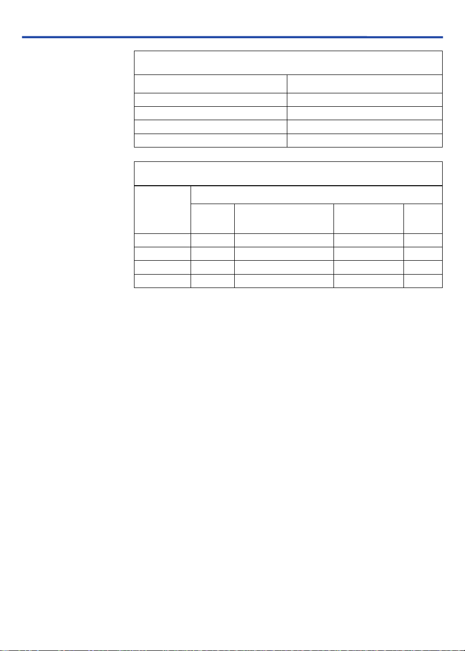
Table 1. MAX 3000A Device Features
Feature EPM3032A EPM3064A EPM3128A EPM3256A
Usable gates 600 1,250 2,500 5,000
Macrocells 32 64 128 256
Logic array blocks 2 4 8 16
Maximum user I/O
pins
(ns) 4.5 4.5 5.0 5.5
t
PD
tSU (ns) 2.9 2.8 3.3 3.9
t
(ns) 3.0 3.1 3.4 3.5
CO1
f
(MHz) 227.3 222.2 192.3 172.4
CNT
Altera Corporation 1
A-DS-M3000A-01.1
34 66 96 158
Page 2

MAX 3000A Programmable Logic Device Family Data Sheet
Programmable macrocell flipflops with individual clear, preset,
...and More Features
■
clock, and clock enable controls
■
Programmable power-saving mode for a power reduction of over
50% in each macrocell
■
Configurable expander product-term distribution, allowing up to
32 product terms per macrocell
■
Programmable security bit for protection of proprietary designs
■
Enhanced architectural features, including:
– 6 pin- or logic-driven output enable signals
– Two global clock signals with optional inversion
– Enhanced interconnect resources for improved routability
– Programmable output slew-rate control
■
Software design support and automatic place-and-route provided by
the Altera® MAX+PLUS® II development system for Windows-based
PCs and Sun SPARCstations, HP 9000 Series 700/800, and IBM RISC
System/6000 workstations
■
Additional design entry and simulation support provided by EDIF
2 0 0 and 3 0 0 netlist files, library of parameterized modules (LPM),
Verilog HDL, VHDL, and other interfaces to popular EDA tools from
third-party manufacturers such as Cadence, Exemplar Logic, Mentor
Graphics, OrCAD, Synopsys, Synplicity, and VeriBest
■
Programming support with the Altera master programming unit
(MPU), MasterBlasterTM communications cable, ByteBlasterMVTM
parallel port download cable, BitBlasterTM serial download cable as
well as programming hardware from third-party manufacturers and
any in-circuit tester that supports JamTM Standard Test and
Programming Language (STAPL) Files (
Files (
.jbc
), or Serial Vector Format Files (
.jam
), Jam STAPL Byte-Code
.svf
)
General Description
2 Altera Corporation
MAX 3000A devices are low-cost, high-performance devices based on the
Altera MAX architecture. Fabricated with advanced CMOS technology,
the EEPROM-based MAX 3000A devices operate with a 3.3-V supply
voltage and provide 600 to 5,000 usable gates, ISP, pin-to-pin delays as
fast as 4.5 ns, and counter speeds of up to 227.3 MHz. MAX 3000A devices
in the -4, -5, -6, -7, and -10 speed grades are compatible with the timing
requirements of the PCI Special Interest Group (PCI SIG)
Specification, Revision 2.2
. See Table 2.
PCI Local Bus
Page 3
MAX 3000A Programmable Logic Device Family Data Sheet
Table 2. MAX 3000A Speed Grades
Device Speed Grade
-4 -5 -6 -7 -10
EPM3032A
EPM3064A
EPM3128A
EPM3256A
Note:
(1) Contact Altera for up-to-date information on the availability of this speed grade.
vvv
vvv
vvv
v (1)
vv
The MAX 3000A architecture supports 100% transistor-to-transistor logic
(TTL) emulation and high-density small-scale integration (SSI),
medium-scale integration (MSI), and large-scale integration (LSI) logic
functions. The MAX 3000A architecture easily integrates multiple devices
ranging from PALs, GALs, and 22V10s to MACH, and pLSI devices.
MAX 3000A devices are available in a wide range of packages, including
PLCC, PQFP, and TQFP packages. See Table 3.
Table 3. MAX 3000A Maximum User I/O Pins
Device 44-Pin
PLCC
EPM3032A 34 34
EPM3064A 34 34 66
EPM3128A 80 96
EPM3256A 116 158
Notes:
(1) Contact Altera for up-to-date information on available device package options.
(2) When the IEEE Std. 1149.1 (JTAG) interface is used for in-system programming or
boundary-scan testing, four I/O pins become JTAG pins.
44-Pin
TQFP
Notes (1), (2)
100-Pin
TQFP
144-Pin
TQFP
208-Pin
PQFP
MAX 3000A devices use CMOS EEPROM cells to implement logic
functions. The user-configurable MAX 3000A architecture accommodates
a variety of independent combinatorial and sequential logic functions.
The devices can be reprogrammed for quick and efficient iterations
during design development and debug cycles, and can be programmed
and erased up to 100 times.
Altera Corporation 3
Page 4

MAX 3000A Programmable Logic Device Family Data Sheet
MAX 3000A devices contain 32 to 256 macrocells, combined into groups
of 16 macrocells called logic array blocks (LABs). Each macrocell has a
programmableindependently programmable clock, clock enable, clear, and preset
functions. To build complex logic functions, each macrocell can be
supplemented with shareable expander and high-speed parallel expander
product terms to provide up to 32 product terms per macrocell.
MAX 3000A devices provide programmable speed/power optimization.
Speed-critical portions of a design can run at high speed/full power,
while the remaining portions run at reduced speed/low power. This
speed/power optimization feature enables the designer to configure one
or more macrocells to operate at 50% or lower power while adding only a
nominal timing delay. MAX 3000A devices also provide an option that
reduces the slew rate of the output buffers, minimizing noise transients
when non-speed-critical signals are switching. The output drivers of all
MAX 3000A devices can be set for 2.5 V or 3.3 V, and all input pins are
2.5-V, 3.3-V, and 5.0-V tolerant, allowing MAX 3000A devices to be used
in mixed-voltage systems.
MAX 3000A devices are supported by the MAX+PLUS II development
system, an integrated package that offers schematic, text—including
VHDL, Verilog HDL, and the Altera Hardware Description Language
(AHDL)—and waveform design entry, compilation and logic synthesis,
simulation and timing analysis, and device programming. The
MAX+PLUS II software provides EDIF 2 0 0 and 3 0 0, LPM, VHDL,
Verilog HDL, and other interfaces for additional design entry and
simulation support from other industry-standard PC- and UNIXworkstation-based EDA tools. The MAX+PLUS II software runs on
Windows-based PCs, as well as Sun SPARCstation, HP 9000 Series
700/800, and IBM RISC System/6000 workstations.
AND
/fixed-OR array and a configurable register with
f
Functional Description
4 Altera Corporation
For more information on development tools, see the
Programmable Logic Development System & Software Data Sheet
The MAX 3000A architecture includes the following elements:
■
Logic array blocks (LABs)
■
Macrocells
■
Expander product terms (shareable and parallel)
■
Programmable interconnect array (PIA)
■
I/O control blocks
The MAX 3000A architecture includes four dedicated inputs that can be
used as general-purpose inputs or as high-speed, global control signals
(clock, clear, and two output enable signals) for each macrocell and I/O
pin. Figure 1 shows the architecture of MAX 3000A devices.
MAX+PLUS II
.
Page 5
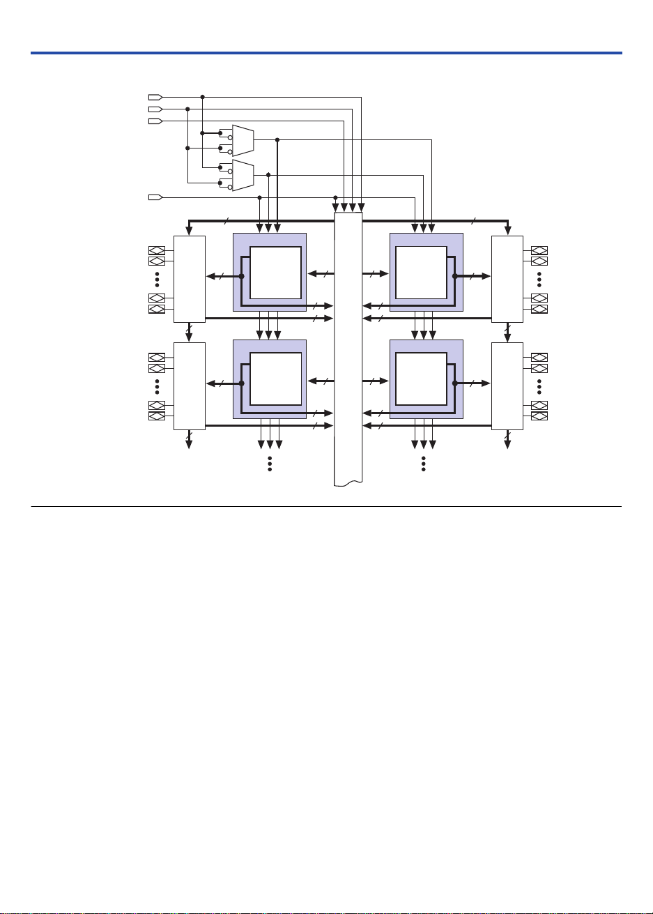
Figure 1. MAX 3000A Device Block Diagram
INPUT/GCLK1
INPUT/OE2/GCLK2
INPUT/OE1
MAX 3000A Programmable Logic Device Family Data Sheet
INPUT/GCLRn
6 to 16 I/O
6 to 16 I/O
6 Output Enables
6 to 16
I/O
Control
Block
6
6 to 16
I/O
Control
Block
6
LAB A
LAB C
Macrocells
1 to 16
Macrocells
33 to 48
36 36
16
6 to 16
36 36
16
6 to 16
16
6 to 16
PIA
16
6 to 16
Macrocells
17 to 32
Macrocells
49 to 64
6 Output Enables
LAB B
6 to 16
Control
LAB D
6 to 16
Control
I/O
Block
I/O
Block
6 to 16 I/O
6
6 to 16 I/O
6
Logic Array Blocks
The MAX 3000A device architecture is based on the linking of
high-performance LABs. LABs consist of 16-macrocell arrays, as shown in
Figure 1. Multiple LABs are linked together via the PIA, a global bus that
is fed by all dedicated input pins, I/O pins, and macrocells.
Each LAB is fed by the following signals:
■
36 signals from the PIA that are used for general logic inputs
■
Global controls that are used for secondary register functions
Macrocells
MAX 3000A macrocells can be individually configured for either
sequential or combinatorial logic operation. Macrocells consist of three
functional blocks: logic array, product-term select matrix, and
programmable register. Figure 2 shows a MAX 3000A macrocell.
Altera Corporation 5
Page 6
MAX 3000A Programmable Logic Device Family Data Sheet
Figure 2. MAX 3000A Macrocell
LAB Local Array
Product-
Term
Select
Matrix
Parallel Logic
Expanders
(from other
macrocells)
Global
Clear
Clear
Select
Global
Clocks
2
VCC
Clock/
Enable
Select
D/T
ENA
PRN
CLRN
Programmable
Register
Register
Bypass
Q
to I/O
Control
Block
36 Signals
from PIA
16 Expander
Product T erms
Shared Logic
Expanders
to PIA
Combinatorial logic is implemented in the logic array, which provides
five product terms per macrocell. The product-term select matrix allocates
these product terms for use as either primary logic inputs (to the OR and
XOR
gates) to implement combinatorial functions, or as secondary inputs
to the macrocell’s register preset, clock, and clock enable control
functions.
Two kinds of expander product terms (“expanders”) are available to
supplement macrocell logic resources:
Shareable expanders, which are inverted product terms that are fed
■
back into the logic array
Parallel expanders, which are product terms borrowed from adjacent
■
macrocells
The MAX+PLUS II development system automatically optimizes
product-term allocation according to the logic requirements of the design.
For registered functions, each macrocell flipflop can be individually
programmed to implement D, T, JK, or SR operation with programmable
clock control. The flipflop can be bypassed for combinatorial operation.
During design entry, the designer specifies the desired flipflop type; the
MAX+PLUS II software then selects the most efficient flipflop operation
for each registered function to optimize resource utilization.
6 Altera Corporation
Page 7

MAX 3000A Programmable Logic Device Family Data Sheet
Each programmable register can be clocked in three different modes:
■
Global clock signal mode, which achieves the fastest clock-to-output
performance.
■
Global clock signal enabled by an active-high clock enable. A clock
enable is generated by a product term. This mode provides an enable
on each flipflop while still achieving the fast clock-to-output
performance of the global clock.
Array clock implemented with a product term. In this mode, the
■
flipflop can be clocked by signals from buried macrocells or I/O pins.
Two global clock signals are available in MAX 3000A devices. As shown
in Figure 1, these global clock signals can be the true or the complement
of either of the two global clock pins,
GCLK1
or
GCLK2
.
Each register also supports asynchronous preset and clear functions. As
shown in Figure 2, the product-term select matrix allocates product terms
to control these operations. Although the product-term-driven preset and
clear from the register are active high, active-low control can be obtained
by inverting the signal within the logic array. In addition, each register
clear function can be individually driven by the active-low dedicated
global clear pin (
GCLRn
).
Expander Product Terms
Although most logic functions can be implemented with the five product
terms available in each macrocell, highly complex logic functions require
additional product terms. Another macrocell can be used to supply the
required logic resources. However, the MAX 3000A architecture also
offers both shareable and parallel expander product terms (“expanders”)
that provide additional product terms directly to any macrocell in the
same LAB. These expanders help ensure that logic is synthesized with the
fewest possible logic resources to obtain the fastest possible speed.
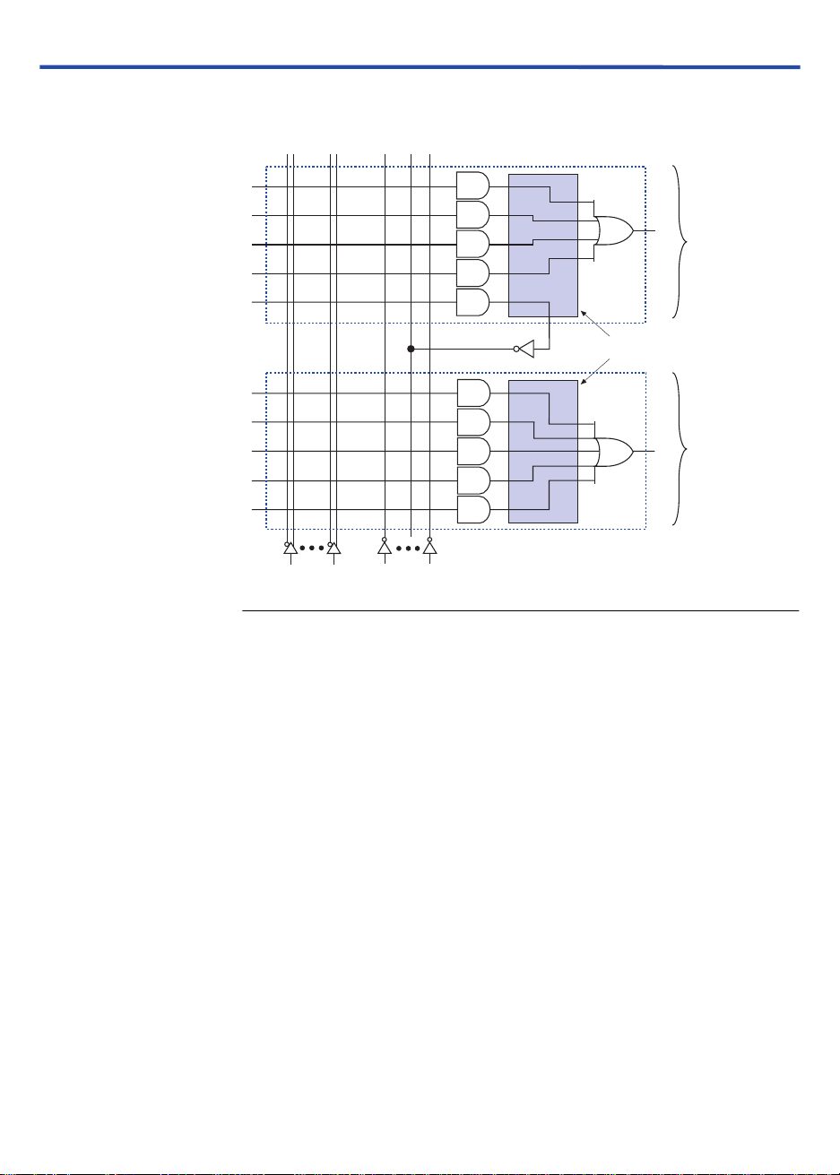
Shareable Expanders
Each LAB has 16 shareable expanders that can be viewed as a pool of
uncommitted single product terms (one from each macrocell) with
inverted outputs that feed back into the logic array. Each shareable
expander can be used and shared by any or all macrocells in the LAB to
build complex logic functions. A small delay (
shareable expanders are used. Figure 3 shows how shareable expanders
can feed multiple macrocells.
t
) is incurred when
SEXP
Altera Corporation 7
Page 8
MAX 3000A Programmable Logic Device Family Data Sheet
Figure 3. MAX 3000A Shareable Expanders
Shareable expanders can be shared by any or all macrocells in an LAB.
Macrocell
Product-Term
Logic
Product-Term Select Matrix
Macrocell
Product-Term
Logic
36 Signals
from PIA
16 Shared
Expanders
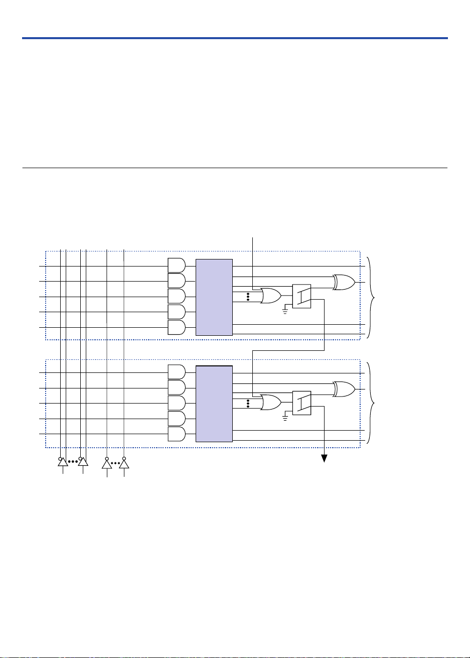
Parallel Expanders
Parallel expanders are unused product terms that can be allocated to a
neighboring macrocell to implement fast, complex logic functions.
Parallel expanders allow up to 20 product terms to directly feed the
macrocell OR logic, with five product terms provided by the macrocell and
15 parallel expanders provided by neighboring macrocells in the LAB.
The MAX+PLUS II Compiler can automatically allocate up to three sets of
up to five parallel expanders to the macrocells that require additional
product terms. Each set of five parallel expanders incurs a small,
incremental timing delay (
product terms, the MAX+PLUS II Compiler uses the five dedicated
product terms within the macrocell and allocates two sets of parallel
expanders; the first set includes five product terms, and the second set
includes four product terms, increasing the total delay by 2 ×
t
). For example, if a macrocell requires 14
PEXP
t
PEXP
.
8 Altera Corporation
Page 9
MAX 3000A Programmable Logic Device Family Data Sheet
Two groups of eight macrocells within each LAB (e.g., macrocells 1
through 8 and 9 through 16) form two chains to lend or borrow parallel
expanders. A macrocell borrows parallel expanders from lowernumbered macrocells. For example, macrocell 8 can borrow parallel
expanders from macrocell 7, from macrocells 7 and 6, or from macrocells
7, 6, and 5. Within each group of eight, the lowest-numbered macrocell
can only lend parallel expanders and the highest-numbered macrocell can
only borrow them. Figure 4 shows how parallel expanders can be
borrowed from a neighboring macrocell.
Figure 4. MAX 3000A Parallel Expanders
Unused product terms in a macrocell can be allocated to a neighboring macrocell.
from
Previous
Macrocell
Preset
36 Signals
from PIA
16 Shared
Expanders
Product-
Term
Select
Matrix
Product-
Term
Select
Matrix
Macrocell
ProductTerm Logic
Clock
Clear
Preset
Macrocell
ProductTerm Logic
Clock
Clear
to Next
Macrocell
Altera Corporation 9
Page 10
MAX 3000A Programmable Logic Device Family Data Sheet
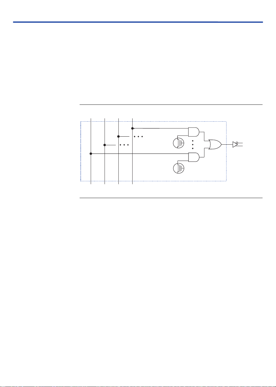
Programmable Interconnect Array
Logic is routed between LABs on the PIA. This global bus is a
programmable path that connects any signal source to any destination on
the device. All MAX 3000A dedicated inputs, I/O pins, and macrocell
outputs feed the PIA, which makes the signals available throughout the
entire device. Only the signals required by each LAB are actually routed
from the PIA into the LAB. Figure 5 shows how the PIA signals are routed
into the LAB. An EEPROM cell controls one input to a 2-input
which selects a PIA signal to drive into the LAB.
Figure 5. MAX 3000A PIA Routing
AND
gate,
to LAB
PIA Signals
While the routing delays of channel-based routing schemes in masked or
field-programmable gate arrays (FPGAs) are cumulative, variable, and
path-dependent, the MAX 3000A PIA has a predictable delay. The PIA
makes a design’s timing performance easy to predict.
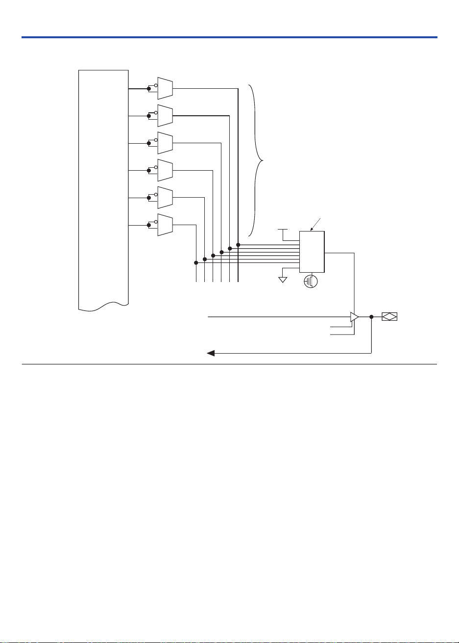
I/O Control Blocks
The I/O control block allows each I/O pin to be individually configured
for input, output, or bidirectional operation. All I/O pins have a tri-state
buffer that is individually controlled by one of the global output enable
signals or directly connected to ground or VCC. Figure 6 shows the I/O
control block for MAX 3000A devices. The I/O control block has
six global output enable signals that are driven by the true or complement
of two output enable signals, a subset of the I/O pins, or a subset of the
I/O macrocells.
10 Altera Corporation
Page 11
MAX 3000A Programmable Logic Device Family Data Sheet
Figure 6. I/O Control Block of MAX 3000A Devices
PIA
6 Global
Output Enable Signals
OE Select Multiplexer
to Other I/O Pins
from
Macrocell
to PIA
VCC
GND
Open-Drain Output
Slew-Rate Control
When the tri-state buffer control is connected to ground, the output is
tri-stated (high impedance) and the I/O pin can be used as a dedicated
input. When the tri-state buffer control is connected to VCC, the output is
enabled.
The MAX 3000A architecture provides dual I/O feedback, in which
macrocell and pin feedbacks are independent. When an I/O pin is
configured as an input, the associated macrocell can be used for buried
logic.
Altera Corporation 11
Page 12

MAX 3000A Programmable Logic Device Family Data Sheet
In-System
Programmability (ISP)
MAX 3000A devices can be programmed in-system via an industrystandard 4-pin IEEE Std. 1149.1-1990 (JTAG) interface. In-system
programmability (ISP) offers quick, efficient iterations during design
development and debugging cycles. The MAX 3000A architecture
internally generates the high programming voltages required to program
its EEPROM cells, allowing in-system programming with only a single
3.3-V power supply. During in-system programming, the I/O pins are tristated and weakly pulled-up to eliminate board conflicts. The pull-up
value is nominally 50 kΩ.
MAX 3000A devices have an enhanced ISP algorithm for faster
programming. These devices also offer an ISP_Done bit that ensures safe
operation when in-system programming is interrupted. This ISP_Done
bit, which is the last bit programmed, prevents all I/O pins from driving
until the bit is programmed.
ISP simplifies the manufacturing flow by allowing devices to be mounted
on a printed circuit board (PCB) with standard pick-and-place equipment
before they are programmed. MAX 3000A devices can be programmed by
downloading the information via in-circuit testers, embedded processors,
the MasterBlaster communications cable, the ByteBlasterMV parallel port
download cable, and the BitBlaster serial download cable. Programming
the devices after they are placed on the board eliminates lead damage on
high-pin-count packages (e.g., QFP packages) due to device handling.
MAX 3000A devices can be reprogrammed after a system has already
shipped to the field. For example, product upgrades can be performed in
the field via software or modem.
The Jam STAPL can be used to program MAX 3000A devices with incircuit testers, PCs, or embedded processors.
f
Programming with External Hardware
f
12 Altera Corporation
For more information on using the Jam STAPL language, see Application
Note 88 (Using the Jam Language for ISP & ICR via an Embedded Processor)
and Application Note 122 (Using Jam STAPL for ISP & ICR via an Embedded
Processor).
MAX 3000A devices can be programmed on Windows-based PCs with an
Altera Logic Programmer card, MPU, and the appropriate device adapter.
The MPU performs continuity checking to ensure adequate electrical
contact between the adapter and the device.
For more information, see the Altera Programming Hardware Data Sheet.
Page 13

MAX 3000A Programmable Logic Device Family Data Sheet
The MAX+PLUS II software can use text- or waveform-format test vectors
created with the MAX+PLUS II Text Editor or Waveform Editor to test the
programmed device. For added design verification, designers can
perform functional testing to compare the functional device behavior with
the results of simulation.
Data I/O, BP Microsystems, and other programming hardware
manufacturers also provide programming support for Altera devices.
f
IEEE Std.
1149.1 (JTAG)
Boundary-Scan
Support
Table 4. MAX 3000A JTAG Instructions
JTAG Instruction Description
SAMPLE/PRELOAD Allows a snapshot of signals at the device pins to be captured and examined during
EXTEST Allows the external circuitry and board-level interconnections to be tested by forcing a
BYPASS Places the 1-bit bypass register between the TDI and TDO pins, which allows the BST
IDCODE Selects the IDCODE register and places it between the TDI and TDO pins, allowing the
USERCODE Selects the 32-bit USERCODE register and places it between the TDI and TDO pins,
ISP Instructions These instructions are used when programming MAX 3000A devices via the JTAG ports
For more information, see Programming Hardware Manufacturers.
MAX 3000A devices include the JTAG BST circuitry defined by IEEE Std.
1149.1-1990. Table 4 describes the JTAG instructions supported by
MAX 3000A devices. The pin-out tables starting on page 39 of this data
sheet show the location of the JTAG control pins for each device. If the
JTAG interface is not required, the JTAG pins are available as user I/O
pins.
normal device operation, and permits an initial data pattern output at the device pins
test pattern at the output pins and capturing test results at the input pins
data to pass synchronously through a selected device to adjacent devices during normal
device operation
IDCODE to be serially shifted out of TDO
allowing the USERCODE value to be shifted out of TDO
with the MasterBlaster, ByteBlasterMV, or BitBlaster cable, or when using a Jam STAPL
file, JBC file, or SVF file via an embedded processor or test equipment
The instruction register length of MAX 3000A devices is 10 bits. The
IDCODE and USERCODE register length is 32 bits. Tables 5 and 6 show
the boundary-scan register length and device IDCODE information for
MAX 3000A devices.
Altera Corporation 13
Page 14
MAX 3000A Programmable Logic Device Family Data Sheet
Table 5. MAX 3000A Boundary-Scan Register Length
Device Boundary-Scan Register Length
EPM3032A 96
EPM3064A 192
EPM3128A 288
EPM3256A 480
Table 6. 32-Bit MAX 3000A Device IDCODE Value Note (1)
Device IDCODE (32 bits)
f
Version
(4 Bits)
EPM3032A 0001 0111 0000 0011 0010 00001101110 1
EPM3064A 0001 0111 0000 0110 0100 00001101110 1
EPM3128A 0001 0111 0001 0010 1000 00001101110 1
EPM3256A 0001 0111 0010 0101 0110 00001101110 1
Notes:
(1) The most significant bit (MSB) is on the left.
(2) The least significant bit (LSB) for all JTAG IDCODEs is 1.
Part Number (16 Bits) Manufacturer’s
Identity (11 Bits)
1 (1 Bit)
(2)
See Application Note 39 (IEEE 1149.1 (JTAG) Boundary-Scan Testing in Altera
Devices) for more information on JTAG BST.
14 Altera Corporation
Page 15
MAX 3000A Programmable Logic Device Family Data Sheet
Figure 7 shows the timing information for the JTAG signals.
Figure 7. MAX 3000A JTAG Waveforms
TMS
TDI
t
JCP
t
JCL
t
JPSU
t
JPH
TCK
t
JCH
t
JPZX
t
JPCO
t
JPXZ
TDO
t
JSH
t
JSCO
t
JSXZ
Signal
to Be
Captured
Signal
to Be
Driven
t
JSZX
t
JSSU
Table 7 shows the JTAG timing parameters and values for MAX 3000A
devices.
Altera Corporation 15
Page 16
MAX 3000A Programmable Logic Device Family Data Sheet
Table 7. JTAG Timing Parameters & Values for MAX 3000A Devices
Symbol Parameter Min Max Unit
t
JCP
t
JCH
t
JCL
t
JPSU
t
JPH
t
JPCO
t
JPZX
t
JPXZ
t
JSSU
t
JSH
t
JSCO
t
JSZX
t
JSXZ
TCK clock period 100 ns
TCK clock high time 50 ns
TCK clock low time 50 ns
JTAG port setup time 20 ns
JTAG port hold time 45 ns
JTAG port clock to output 25 ns
JTAG port high impedance to valid output 25 ns
JTAG port valid output to high impedance 25 ns
Capture register setup time 20 ns
Capture register hold time 45 ns
Update register clock to output 25 ns
Update register high impedance to valid output 25 ns
Update register valid output to high impedance 25 ns
Programmable Speed/Power Control
Output
Configuration
MAX 3000A devices offer a power-saving mode that supports low-power
operation across user-defined signal paths or the entire device. This
feature allows total power dissipation to be reduced by 50% or more
because most logic applications require only a small fraction of all gates to
operate at maximum frequency.
The designer can program each individual macrocell in a MAX 3000A
device for either high-speed or low-power operation. As a result, speedcritical paths in the design can run at high speed, while the remaining
paths can operate at reduced power. Macrocells that run at low power
incur a nominal timing delay adder (t
t
CPPW
and t
parameters.
SEXP
) for the t
LPA
LAD
, t
LAC
, tIC, t
ACL
, tEN,
MAX 3000A device outputs can be programmed to meet a variety of
system-level requirements.
MultiVolt I/O Interface
The MAX 3000A device architecture supports the MultiVolt I/O interface
feature, which allows MAX 3000A devices to connect to systems with
differing supply voltages. MAX 3000A devices in all packages can be set
for 2.5-V, 3.3-V, or 5.0-V I/O pin operation. These devices have one set of
VCC pins for internal operation and input buffers (VCCINT), and another
set for I/O output drivers (VCCIO).
16 Altera Corporation
Page 17

MAX 3000A Programmable Logic Device Family Data Sheet
The VCCIO pins can be connected to either a 3.3-V or 2.5-V power supply,
depending on the output requirements. When the VCCIO pins are
connected to a 2.5-V power supply, the output levels are compatible with
2.5-V systems. When the VCCIO pins are connected to a 3.3-V power
supply, the output high is at 3.3 V and is therefore compatible with 3.3-V
or 5.0-V systems. Devices operating with V
incur a nominally greater timing delay of t
levels lower than 3.0 V
CCIO
instead of t
OD2
OD1
. Inputs can
always be driven by 2.5-V, 3.3-V, or 5.0-V signals.
Table 8 summarizes the MAX 3000A MultiVolt I/O support.
Table 8. MAX 3000A MultiVolt I/O Support
Voltage Input Signal (V) Output Signal (V)
V
CCIO
2.5 3.3 5.0 2.5 3.3 5.0
2.5
3.3
Note:
(1) When V
tolerant inputs.
CCIO
vvvv
(1)
vvv
is 3.3 V, a MAX 3000A device can drive a 2.5-V device that has 3.3-V
v
vv
Open-Drain Output Option
MAX 3000A devices provide an optional open-drain (equivalent to
open-collector) output for each I/O pin. This open-drain output enables
the device to provide system-level control signals (e.g., interrupt and
write enable signals) that can be asserted by any of several devices. It can
also provide an additional wired-OR plane.
Slew-Rate Control
The output buffer for each MAX 3000A I/O pin has an adjustable output
slew rate that can be configured for low-noise or high-speed performance.
A faster slew rate provides high-speed transitions for high-performance
systems. However, these fast transitions may introduce noise transients
into the system. A slow slew rate reduces system noise, but adds a
nominal delay of 4 to 5 ns. When the configuration cell is turned off, the
slew rate is set for low-noise performance. Each I/O pin has an individual
EEPROM bit that controls the slew rate, allowing designers to specify the
slew rate on a pin-by-pin basis. The slew rate control affects both the
rising and falling edges of the output signal.
Altera Corporation 17
Page 18

MAX 3000A Programmable Logic Device Family Data Sheet
CC
Design Security
Generic Testing
All MAX 3000A devices contain a programmable security bit that controls
access to the data programmed into the device. When this bit is
programmed, a design implemented in the device cannot be copied or
retrieved. This feature provides a high level of design security because
programmed data within EEPROM cells is invisible. The security bit that
controls this function, as well as all other programmed data, is reset only
when the device is reprogrammed.
MAX 3000A devices are fully functionally tested. Complete testing of
each programmable EEPROM bit and all internal logic elements ensures
100% programming yield. AC test measurements are taken under
conditions equivalent to those shown in Figure 8. Test patterns can be
used and then erased during early stages of the production flow.
Figure 8. MAX 3000A AC Test Conditions
Power supply transients can affect AC
measurements. Simultaneous transitions
of multiple outputs should be avoided for
accurate measurement. Threshold tests
must not be performed under AC
conditions. Large-amplitude, fast-groundcurrent transients normally occur as the
device outputs discharge the load
capacitances. When these transients flow
through the parasitic inductance between
the device ground pin and the test system
ground, significant reductions in
observable noise immunity can result.
Numbers in brackets are for 2.5-V
outputs. Numbers without brackets are for
3.3-V devices or outputs.
703 Ω
[521 Ω]
Device
Output
620 Ω
[481 Ω]
Device input
rise and fall
times < 2 ns
V
to Test
System
C1 (includes JIG
capacitance)
Operating Conditions
Tables 9 through 12 provide information on absolute maximum ratings,
recommended operating conditions, DC operating conditions, and
capacitance for MAX 3000A devices.
Table 9. MAX 3000A Device Absolute Maximum Ratings Note (1)
Symbol Parameter Conditions Min Max Unit
V
V
I
OUT
T
T
T
18 Altera Corporation
Supply voltage With respect to ground (2) –0.5 4.6 V
CC
DC input voltage –2.0 5.75 V
I
DC output current, per pin –25 25 mA
Storage temperature No bias –65 150 ° C
STG
Ambient temperature Under bias –65 135 ° C
A
Junction temperature PQFP and TQFP packages, under bias 135 ° C
J
Page 19

MAX 3000A Programmable Logic Device Family Data Sheet
Table 10. MAX 3000A Device Recommended Operating Conditions
Symbol Parameter Conditions Min Max Unit
V
V
V
V
V
T
T
t
R
t
F
Supply voltage for internal logic and
CCINT
input buffers
Supply voltage for output drivers,
CCIO
3.3-V operation
Supply voltage for output drivers,
3.0 3.6 V
3.0 3.6 V
2.3 2.7 V
2.5-V operation
Supply voltage during ISP 3.0 3.6 V
CCISP
Input voltage (3) –0.5 5.75 V
I
Output voltage 0 V
O
Ambient temperature For commercial use 0 70 ° C
A
For industrial use –40 85 ° C
Junction temperature For commercial use 0 90 ° C
J
For industrial use –40 105 ° C
Input rise time 40 ns
Input fall time 40 ns
CCIO
V
Table 11. MAX 3000A Device DC Operating Conditions Note (4)
Symbol Parameter Conditions Min Max Unit
V
V
V
V
I
I
I
OZ
R
High-level input voltage 1.7 5.75 V
IH
Low-level input voltage –0.5 0.8 V
IL
3.3-V high-level TTL output voltage IOH = –8 mA DC, V
OH
3.3-V high-level CMOS output
voltage
2.5-V high-level output voltage I
3.3-V low-level TTL output voltage IOL = 8 mA DC, V
OL
3.3-V low-level CMOS output
voltage
2.5-V low-level output voltage I
Input leakage current VI = V
Tri-state output off-state current VO = V
Value of I/O pin pull-up resistor
ISP
when programming in-system or
= –0.1 mA DC, V
I
OH
= –100 µA DC, V
OH
= –1 mA DC, V
I
OH
= –2 mA DC, V
I
OH
= 0.1 mA DC, V
I
OL
= 100 µA DC, V
OL
= 1 mA DC, V
I
OL
= 2 mA DC, V
I
OL
or ground –10 10 µA
CCINT
or ground –10 10 µA
CCINT
V
= 2.3 to 3.6 V (7) 20 74 kΩ
CCIO
= 3.00 V (5) 2.4 V
CCIO
= 3.00 V (5) V
CCIO
= 2.30 V (5) 2.1 V
CCIO
= 2.30 V (5) 2.0 V
CCIO
= 2.30 V (5) 1.7 V
CCIO
= 3.00 V (6) 0.4 V
CCIO
= 3.00 V (6) 0.2 V
CCIO
= 2.30 V (6) 0.2 V
CCIO
= 2.30 V (6) 0.4 V
CCIO
= 2.30 V (6) 0.7 V
CCIO
– 0.2 V
CCIO
during power-up
Altera Corporation 19
Page 20

MAX 3000A Programmable Logic Device Family Data Sheet
Table 12. MAX 3000A Device Capacitance Note (8)
Symbol Parameter Conditions Min Max Unit
C
C
Notes to tables:
(1) See the Operating Requirements for Altera Devices Data Sheet.
(2) Minimum DC input voltage is –0.5 V. During transitions, the inputs may undershoot to –2.0 V or overshoot to
(3) All pins, including dedicated inputs, I/O pins, and JTAG pins, may be driven before V
(4) These values are specified under the recommended operating conditions, as shown in Table 10 on page 19.
(5) The parameter is measured with 50% of the outputs each sourcing the specified current. The I
(6) The parameter is measured with 50% of the outputs each sinking the specified current. The I
(7) This pull-up exists while devices are programmed in-system and in unprogrammed devices during power-up.
(8) Capacitance is measured at 25° C and is sample-tested only. The
Input pin capacitance VIN = 0 V, f = 1.0 MHz 8 pF
IN
I/O pin capacitance V
I/O
= 0 V, f = 1.0 MHz 8 pF
OUT
5.75 V for input currents less than 100 mA and periods shorter than 20 ns.
and V
powered.
CCINT
to high-level TTL or CMOS output current.
low-level TTL or CMOS output current.
OE1 pin (high-voltage pin during programming)
OL
has a maximum capacitance of 20 pF.
are
CCIO
parameter refers
OH
parameter refers to
Figure 9 shows the typical output drive characteristics of MAX 3000A
devices.
20 Altera Corporation
Page 21

MAX 3000A Programmable Logic Device Family Data Sheet
Figure 9. Output Drive Characteristics of MAX 3000A Devices
3.3 V
150
I
OL
Typical I
Output
O
Current (mA)
2.5 V
Typical I
Output
O
Current (mA)
100
150
100
V
= 3.3
= 3.3 V
I
OH
V
O
= 25 C
CCINT
V
CCIO
Temperature
50
0
0
1234
VO Output Voltage (V)
I
OL
V
= 3.3 V
CCINT
V
= 2.5 V
CCIO
Temperature
50
I
OH
0
0
1234
O
= 25 C
VO Output Voltage (V)
Power Sequencing & Hot-Socketing
Because MAX 3000A devices can be used in a mixed-voltage
environment, they have been designed specifically to tolerate any
possible power-up sequence. The V
CCIO
and V
power planes can be
CCINT
powered in any order.
Signals can be driven into MAX 3000A devices before and during
power-up without damaging the device. In addition, MAX 3000A devices
do not drive out during power-up. Once operating conditions are
reached, MAX 3000A devices operate as specified by the user.
Altera Corporation 21
Page 22

MAX 3000A Programmable Logic Device Family Data Sheet
Timing Model
MAX 3000A device timing can be analyzed with the MAX+PLUS II
software, with a variety of popular industry-standard EDA simulators
and timing analyzers, or with the timing model shown in Figure 10.
MAX 3000A devices have predictable internal delays that enable the
designer to determine the worst-case timing of any design. The software
provides timing simulation, point-to-point delay prediction, and detailed
timing analysis for device-wide performance evaluation.
Figure 10. MAX 3000A Timing Model
Input
Delay
t
IN
PIA
Delay
t
PIA
Internal Output
Enable Delay
t
IOE
Global Control
Delay
t
GLOB
Logic Array
Delay
t
LAD
Register
Control Delay
t
LAC
t
IC
t
EN
Shared
Expander Delay
t
SEXP
Parallel
Expander Delay
t
PEXP
Register
Delay
t
SU
t
H
t
PRE
t
CLR
t
RD
t
COMB
Output
Delay
t
OD1
t
OD2
t
OD3
t
XZ
t
X1
Z
t
ZX2
t
ZX3
I/O
Delay
t
IO
The timing characteristics of any signal path can be derived from the
timing model and parameters of a particular device. External timing
parameters, which represent pin-to-pin timing delays, can be calculated
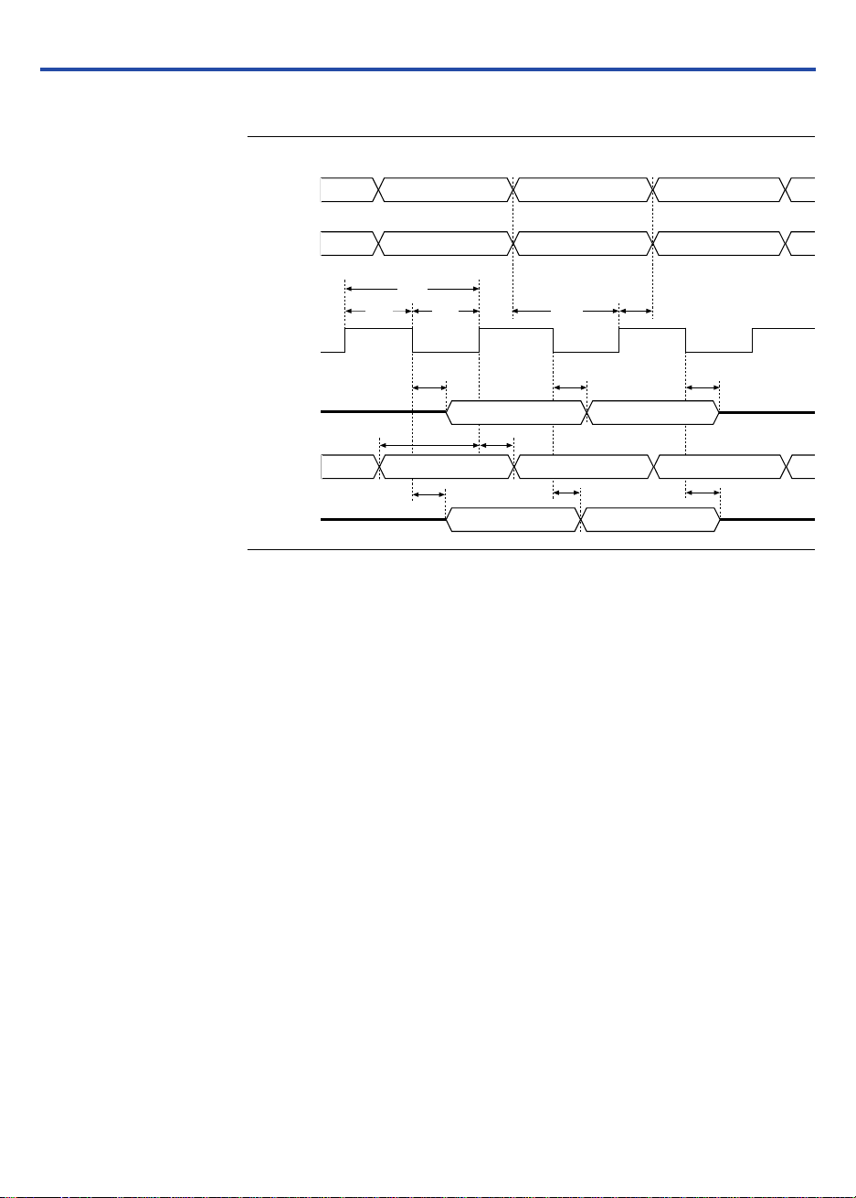
as the sum of internal parameters. Figure 11 shows the timing relationship
between internal and external delay parameters.
22 Altera Corporation
Page 23

Figure 11. MAX 3000A Switching Waveforms
MAX 3000A Programmable Logic Device Family Data Sheet
tR & tF < 2 ns. Inputs are
driven at 3 V for a logic
high and 0 V for a logic
low. All timing
characteristics are
measured at 1.5 V.
Input Pin
I/O Pin
PIA Delay
Shared Expander
Parallel Expander
Delay
Logic Array
Input
Delay
Logic Array
Output
Output Pin
Global
Clock Pin
Global Clock
at Register
Data or Enable
(Logic Array Output)
Combinatorial Mode
t
IN
t
IO
Global Clock Mode
t
IN
tSUt
t
CH
t
GLOB
H
t
R
t
PIA
t
SEXP
t
, t
LAC
LAD
t
PEXP
t
COMB
t
OD
t
CL
t
F
Array Clock Mode
t
F
t
CLR
, t
PRE
t
PIA
t
OD
Input or I/O Pin
Clock into PIA
Clock into
Logic Array
Clock at
Register
Data from
Logic Array
Register to PIA
to Logic Array
Register Output
to Pin
t
R
t
ACH
t
IN
t
IO
t
PIA
t
ACL
t
IC
t
t
SU
H
t
RD
t
PIA
t
OD
Altera Corporation 23
Page 24

MAX 3000A Programmable Logic Device Family Data Sheet
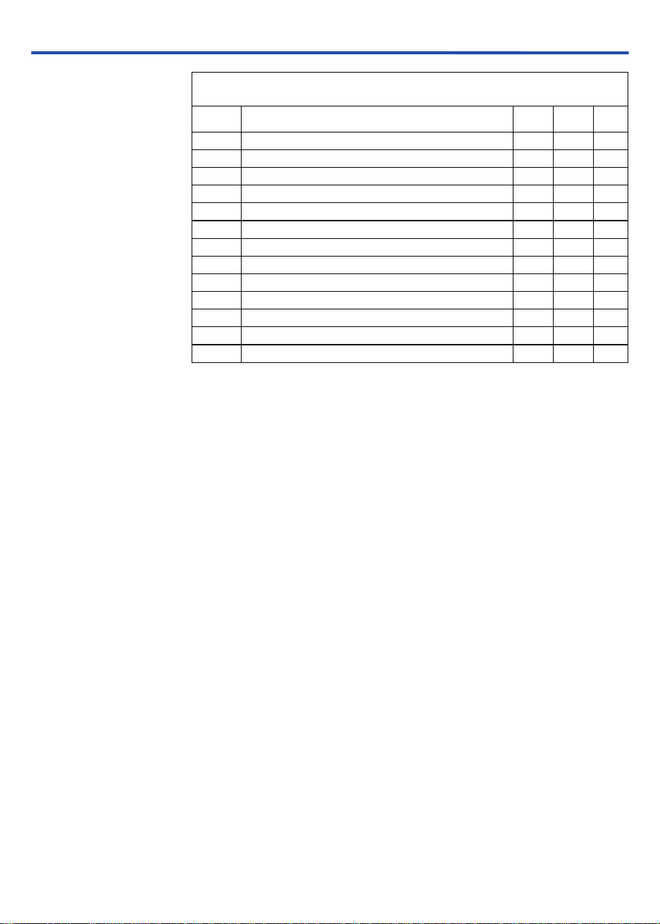
Tables 13 through 20 show EPM3032AE, EPM3064A, EPM3128A, and
EPM3256A timing information.
Table 13. EPM3032A External Timing Parameters Note (1)
Symbol Parameter Conditions Speed Grade Unit
-4 -7 -10
Min Max Min Max Min Max
t
PD1
t
PD2
t
SU
t
H
t
CO1
t
CH
t
CL
t
ASU
t
AH
t
ACO1
t
ACH
t
ACL
t
CPPW
t
CNT
f
CNT
t
ACNT
f
ACNT
Input to nonregistered output
I/O input to nonregistered output
Global clock setup
C1 = 35 pF
4.5 7.5 10 ns
(2)
C1 = 35 pF
4.5 7.5 10 ns
(2)
(2) 2.9 4.7 6.3 ns
time
Global clock hold time (2) 0.0 0.0 0.0 ns
Global clock to output
C1 = 35 pF 1.0 3.0 1.0 5.0 1.0 6.7 ns
delay
Global clock high time 2.0 3.0 4.0 ns
Global clock low time 2.0 3.0 4.0 ns
Array clock setup time (2) 1.6 2.5 3.6 ns
Array clock hold time (2) 0.3 0.5 0.5 ns
Array clock to output
delay
C1 = 35 pF
(2)
1.0 4.3 1.0 7.2 1.0 9.4 ns
Array clock high time 2.0 3.0 4.0 ns
Array clock low time 2.0 3.0 4.0 ns
Minimum pulse width
(3) 2.0 3.0 4.0 ns
for clear and preset
Minimum global clock
(2) 4.4 7.2 9.7 ns
period
Maximum internal
(2), (4) 227.3 138.9 103.1 MHz
global clock frequency
Minimum array clock
(2) 4.4 7.2 9.7 ns
period
Maximum internal
(2), (4) 227.3 138.9 103.1 MHz
array clock frequency
24 Altera Corporation
Page 25

MAX 3000A Programmable Logic Device Family Data Sheet
Table 14. EPM3032A Internal Timing Parameters (Part 1 of 2) Note (1)
Symbol Parameter Conditions Speed Grade Unit
-4 -7 -10
Min Max Min Max Min Max
t
IN
t
IO
t
SEXP
t
PEXP
t
LAD
t
LAC
t
IOE
t
OD1
t
OD2
t
OD3
t
ZX1
t
ZX2
t
ZX3
t
XZ
t
SU
t
H
t
RD
t
COMB
t
IC
t
EN
t
GLOB
t
PRE
t
CLR
Input pad and buffer delay 0.7 1.2 1.5 ns
I/O input pad and buffer
0.7 1.2 1.5 ns
delay
Shared expander delay 1.9 3.1 4.0 ns
Parallel expander delay 0.5 0.8 1.0 ns
Logic array delay 1.5 2.5 3.3 ns
Logic control array delay 0.6 1.0 1.2 ns
Internal output enable delay 0.0 0.0 0.0 ns
Output buffer and pad
C1 = 35 pF 0.8 1.3 1.8 ns
delay, slow slew rate = off
V
= 3.3 V
CCIO
Output buffer and pad
C1 = 35 pF 1.3 1.8 2.3 ns
delay, slow slew rate = off
= 2.5 V
V
CCIO
Output buffer and pad
C1 = 35 pF 5.8 6.3 6.8 ns
delay, slow slew rate = on
V
= 2.5 V or 3.3 V
CCIO
Output buffer enable delay,
C1 = 35 pF 4.0 4.0 5.0 ns
slow slew rate = off
V
= 3.3 V
CCIO
Output buffer enable delay,
C1 = 35 pF 4.5 4.5 5.5 ns
slow slew rate = off
V
= 2.5 V
CCIO
Output buffer enable delay,
C1 = 35 pF 9.0 9.0 10.0 ns
slow slew rate = on
= 2.5 V or 3.3 V
V
CCIO
Output buffer disable delay C1 = 5 pF 4.0 4.0 5.0 ns
Register setup time 1.3 2.0 2.8 ns
Register hold time 0.6 1.0 1.3 ns
Register delay 0.7 1.2 1.5 ns
Combinatorial delay 0.6 1.0 1.3 ns
Array clock delay 1.2 2.0 2.5 ns
Register enable time 0.6 1.0 1.2 ns
Global control delay 0.8 1.3 1.9 ns
Register preset time 1.2 1.9 2.6 ns
Register clear time 1.2 1.9 2.6 ns
Altera Corporation 25
Page 26

MAX 3000A Programmable Logic Device Family Data Sheet
Table 14. EPM3032A Internal Timing Parameters (Part 2 of 2) Note (1)
Symbol Parameter Conditions Speed Grade Unit
-4 -7 -10
Min Max Min Max Min Max
t
t
PIA
LPA
PIA delay (2) 0.9 1.5 2.1 ns
Low-power adder (5) 2.5 4.0 5.0 ns
26 Altera Corporation
Page 27

MAX 3000A Programmable Logic Device Family Data Sheet
Table 15. EPM3064A External Timing Parameters Note (1)
Symbol Parameter Conditions Speed Grade Unit
-4 -7 -10
Min Max Min Max Min Max
t
PD1
t
PD2
t
SU
t
H
t
CO1
t
CH
t
CL
t
ASU
t
AH
t
ACO1
t
ACH
t
ACL
t
CPPW
t
CNT
f
CNT
t
ACNT
f
ACNT
Input to nonregistered output
I/O input to nonregistered output
Global clock setup
C1 = 35 pF
4.5 7.5 10.0 ns
(2)
C1 = 35 pF
4.5 7.5 10.0 ns
(2)
(2) 2.8 4.7 6.2 ns
time
Global clock hold time (2) 0.0 0.0 0.0 ns
Global clock to output
C1 = 35 pF 1.0 3.1 1.0 5.1 1.0 7.0 ns
delay
Global clock high time 2.0 3.0 4.0 ns
Global clock low time 2.0 3.0 4.0 ns
Array clock setup time (2) 1.6 2.6 3.6 ns
Array clock hold time (2) 0.3 0.4 0.6 ns
Array clock to output
delay
C1 = 35 pF
(2)
1.0 4.3 1.0 7.2 1.0 9.6 ns
Array clock high time 2.0 3.0 4.0 ns
Array clock low time 2.0 3.0 4.0 ns
Minimum pulse width
(3) 2.0 3.0 4.0 ns
for clear and preset
Minimum global clock
(2) 4.5 7.4 10.0 ns
period
Maximum internal
(2), (4) 222.2 135.1 100.0 MHz
global clock frequency
Minimum array clock
(2) 4.5 7.4 10.0 ns
period
Maximum internal
(2), (4) 222.2 135.1 100.0 MHz
array clock frequency
Altera Corporation 27
Page 28

MAX 3000A Programmable Logic Device Family Data Sheet
Table 16. EPM3064A Internal Timing Parameters (Part 1 of 2) Note (1)
Symbol Parameter Conditions Speed Grade Unit
-4 -7 -10
Min Max Min Max Min Max
t
IN
t
IO
t
SEXP
t
PEXP
t
LAD
t
LAC
t
IOE
t
OD1
t
OD2
t
OD3
t
ZX1
t
ZX2
t
ZX3
t
XZ
t
SU
t
H
t
RD
t
COMB
t
IC
t
EN
t
GLOB
t
PRE
t
CLR
Input pad and buffer delay 0.6 1.1 1.4 ns
I/O input pad and buffer
0.6 1.1 1.4 ns
delay
Shared expander delay 1.8 3.0 3.9 ns
Parallel expander delay 0.4 0.7 0.9 ns
Logic array delay 1.5 2.5 3.2 ns
Logic control array delay 0.6 1.0 1.2 ns
Internal output enable delay 0.0 0.0 0.0 ns
Output buffer and pad
C1 = 35 pF 0.8 1.3 1.8 ns
delay, slow slew rate = off
V
= 3.3 V
CCIO
Output buffer and pad
C1 = 35 pF 1.3 1.8 2.3 ns
delay, slow slew rate = off
V
= 2.5 V
CCIO
Output buffer and pad
C1 = 35 pF 5.8 6.3 6.8 ns
delay, slow slew rate = on
V
= 2.5 V or 3.3 V
CCIO
Output buffer enable delay,
C1 = 35 pF 4.0 4.0 5.0 ns
slow slew rate = off
V
= 3.3 V
CCIO
Output buffer enable delay,
C1 = 35 pF 4.5 4.5 5.5 ns
slow slew rate = off
V
= 2.5 V
CCIO
Output buffer enable delay,
C1 = 35 pF 9.0 9.0 10.0 ns
slow slew rate = on
V
= 2.5 V or 3.3 V
CCIO
Output buffer disable delay C1 = 5 pF 4.0 4.0 5.0 ns
Register setup time 1.3 2.0 2.9 ns
Register hold time 0.6 1.0 1.3 ns
Register delay 0.7 1.2 1.6 ns
Combinatorial delay 0.6 0.9 1.3 ns
Array clock delay 1.2 1.9 2.5 ns
Register enable time 0.6 1.0 1.2 ns
Global control delay 1.0 1.5 2.2 ns
Register preset time 1.3 2.1 2.9 ns
Register clear time 1.3 2.1 2.9 ns
28 Altera Corporation
Page 29

MAX 3000A Programmable Logic Device Family Data Sheet
Table 16. EPM3064A Internal Timing Parameters (Part 2 of 2) Note (1)
Symbol Parameter Conditions Speed Grade Unit
-4 -7 -10
Min Max Min Max Min Max
t
PIA
t
LPA
PIA delay (2) 1.0 1.7 2.3 ns
Low-power adder (5) 3.5 4.0 5.0 ns
Altera Corporation 29
Page 30

MAX 3000A Programmable Logic Device Family Data Sheet
Table 17. EPM3128A External Timing Parameters Note (1)
Symbol Parameter Conditions Speed Grade Unit
-5 -7 -10
Min Max Min Max Min Max
t
PD1
t
PD2
t
SU
t
H
t
CO1
t
CH
t
CL
t
ASU
t
AH
t
ACO1
t
ACH
t
ACL
t
CPPW
t
CNT
f
CNT
t
ACNT
f
ACNT
Input to nonregistered output
I/O input to nonregistered output
Global clock setup
C1 = 35 pF
5.0 7.5 10 ns
(2)
C1 = 35 pF
5.0 7.5 10 ns
(2)
(2) 3.3 4.9 6.6 ns
time
Global clock hold time (2) 0.0 0.0 0.0 ns
Global clock to output
C1 = 35 pF 1.0 3.4 1.0 5.0 1.0 6.6 ns
delay
Global clock high time 2.0 3.0 4.0 ns
Global clock low time 2.0 3.0 4.0 ns
Array clock setup time (2) 1.8 2.8 3.8 ns
Array clock hold time (2) 0.2 0.3 0.4 ns
Array clock to output
delay
C1 = 35 pF
(2)
1.0 4.9 1.0 7.1 1.0 9.4 ns
Array clock high time 2.0 3.0 4.0 ns
Array clock low time 2.0 3.0 4.0 ns
Minimum pulse width
(3) 2.0 3.0 4.0 ns
for clear and preset
Minimum global clock
(2) 5.2 7.7 10.2 ns
period
Maximum internal
(2), (4) 192.3 129.9 98.0 MHz
global clock frequency
Minimum array clock
(2) 5.2 7.7 10.2 ns
period
Maximum internal
(2), (4) 192.3 129.9 98.0 MHz
array clock frequency
30 Altera Corporation
Page 31

MAX 3000A Programmable Logic Device Family Data Sheet
Table 18. EPM3128A Internal Timing Parameters (Part 1 of 2) Note (1)
Symbol Parameter Conditions Speed Grade Unit
-5 -7 -10
Min Max Min Max Min Max
t
IN
t
IO
t
SEXP
t
PEXP
t
LAD
t
LAC
t
IOE
t
OD1
t
OD2
t
OD3
t
ZX1
t
ZX2
t
ZX3
t
XZ
t
SU
t
H
t
RD
t
COMB
t
IC
t
EN
t
GLOB
t
PRE
t
CLR
Input pad and buffer delay 0.7 1.0 1.4 ns
I/O input pad and buffer
0.7 1.0 1.4 ns
delay
Shared expander delay 2.0 2.9 3.8 ns
Parallel expander delay 0.4 0.7 0.9 ns
Logic array delay 1.6 2.4 3.1 ns
Logic control array delay 0.7 1.0 1.3 ns
Internal output enable delay 0.0 0.0 0.0 ns
Output buffer and pad
C1 = 35 pF 0.8 1.2 1.6 ns
delay, slow slew rate = off
V
= 3.3 V
CCIO
Output buffer and pad
C1 = 35 pF 1.3 1.7 2.1 ns
delay, slow slew rate = off
V
= 2.5 V
CCIO
Output buffer and pad
C1 = 35 pF 5.8 6.2 6.6 ns
delay, slow slew rate = on
V
= 2.5 V or 3.3 V
CCIO
Output buffer enable delay,
C1 = 35 pF 4.0 4.0 5.0 ns
slow slew rate = off
= 3.3 V
V
CCIO
Output buffer enable delay,
C1 = 35 pF 4.5 4.5 5.5 ns
slow slew rate = off
V
= 2.5 V
CCIO
Output buffer enable delay,
C1 = 35 pF 9.0 9.0 10.0 ns
slow slew rate = on
V
= 2.5 V or 3.3 V
CCIO
Output buffer disable delay C1 = 5 pF 4.0 4.0 5.0 ns
Register setup time 1.4 2.1 2.9 ns
Register hold time 0.6 1.0 1.3 ns
Register delay 0.8 1.2 1.6 ns
Combinatorial delay 0.5 0.9 1.3 ns
Array clock delay 1.2 1.7 2.2 ns
Register enable time 0.7 1.0 1.3 ns
Global control delay 1.1 1.6 2.0 ns
Register preset time 1.4 2.0 2.7 ns
Register clear time 1.4 2.0 2.7 ns
Altera Corporation 31
Page 32

MAX 3000A Programmable Logic Device Family Data Sheet
Table 18. EPM3128A Internal Timing Parameters (Part 2 of 2) Note (1)
Symbol Parameter Conditions Speed Grade Unit
-5 -7 -10
Min Max Min Max Min Max
t
t
PIA
LPA
PIA delay (2) 1.4 2.0 2.6 ns
Low-power adder (5) 4.0 4.0 5.0 ns
32 Altera Corporation
Page 33

MAX 3000A Programmable Logic Device Family Data Sheet
Table 19. EPM3256A External Timing Parameters Note (1)
Symbol Parameter Conditions Speed Grade Unit
-5 -7 -10
Min Max Min Max Min Max
t
PD1
t
PD2
t
SU
t
H
t
CO1
t
CH
t
CL
t
ASU
t
AH
t
ACO1
t
ACH
t
ACL
t
CPPW
t
CNT
f
CNT
t
ACNT
f
ACNT
Input to nonregistered output
I/O input to nonregistered output
Global clock setup
C1 = 35 pF
5.5 7.5 10 ns
(2)
C1 = 35 pF
5.5 7.5 10 ns
(2)
(2) 3.9 5.2 6.9 ns
time
Global clock hold time (2) 0.0 0.0 0.0 ns
Global clock to output
C1 = 35 pF 1.0 3.5 1.0 4.8 1.0 6.4 ns
delay
Global clock high time 2.0 3.0 4.0 ns
Global clock low time 2.0 3.0 4.0 ns
Array clock setup time (2) 2.0 2.7 3.6 ns
Array clock hold time (2) 0.2 0.3 0.5 ns
Array clock to output
delay
C1 = 35 pF
(2)
1.0 5.4 1.0 7.3 1.0 9.7 ns
Array clock high time 2.0 3.0 4.0 ns
Array clock low time 2.0 3.0 4.0 ns
Minimum pulse width
(3) 2.0 3.0 4.0 ns
for clear and preset
Minimum global clock
(2) 5.8 7.9 10.5 ns
period
Maximum internal
(2), (4) 172.4 126.6 95.2 MHz
global clock frequency
Minimum array clock
(2) 5.8 7.9 10.5 ns
period
Maximum internal
(2), (4) 172.4 126.6 95.2 MHz
array clock frequency
Altera Corporation 33
Page 34

MAX 3000A Programmable Logic Device Family Data Sheet
Table 20. EPM3256A Internal Timing Parameters (Part 1 of 2) Note (1)
Symbol Parameter Conditions Speed Grade Unit
-5 -7 -10
Min Max Min Max Min Max
t
IN
t
IO
t
SEXP
t
PEXP
t
LAD
t
LAC
t
IOE
t
OD1
t
OD2
t
OD3
t
ZX1
t
ZX2
t
ZX3
t
XZ
t
SU
t
H
t
RD
t
COMB
t
IC
t
EN
t
GLOB
t
PRE
t
CLR
Input pad and buffer delay 0.7 0.9 1.2 ns
I/O input pad and buffer
0.7 0.9 1.2 ns
delay
Shared expander delay 2.1 2.8 3.7 ns
Parallel expander delay 0.3 0.5 0.6 ns
Logic array delay 1.7 2.2 2.8 ns
Logic control array delay 0.8 1.0 1.3 ns
Internal output enable delay 0.0 0.0 0.0 ns
Output buffer and pad
C1 = 35 pF 0.9 1.2 1.6 ns
delay, slow slew rate = off
V
= 3.3 V
CCIO
Output buffer and pad
C1 = 35 pF 1.4 1.7 2.1 ns
delay, slow slew rate = off
V
= 2.5 V
CCIO
Output buffer and pad
C1 = 35 pF 5.9 6.2 6.6 ns
delay, slow slew rate = on
V
= 2.5 V or 3.3 V
CCIO
Output buffer enable delay,
C1 = 35 pF 4.0 4.0 5.0 ns
slow slew rate = off
V
= 3.3 V
CCIO
Output buffer enable delay,
C1 = 35 pF 4.5 4.5 5.5 ns
slow slew rate = off
V
= 2.5 V
CCIO
Output buffer enable delay,
C1 = 35 pF 9.0 9.0 10.0 ns
slow slew rate = on
V
= 2.5 V or 3.3 V
CCIO
Output buffer disable delay C1 = 5 pF 4.0 4.0 5.0 ns
Register setup time 1.5 2.1 2.9 ns
Register hold time 0.7 0.9 1.2 ns
Register delay 0.9 1.2 1.6 ns
Combinatorial delay 0.5 0.8 1.2 ns
Array clock delay 1.2 1.6 2.1 ns
Register enable time 0.8 1.0 1.3 ns
Global control delay 1.0 1.5 2.0 ns
Register preset time 1.6 2.3 3.0 ns
Register clear time 1.6 2.3 3.0 ns
34 Altera Corporation
Page 35

MAX 3000A Programmable Logic Device Family Data Sheet
Table 20. EPM3256A Internal Timing Parameters (Part 2 of 2) Note (1)
Symbol Parameter Conditions Speed Grade Unit
-5 -7 -10
Min Max Min Max Min Max
t
PIA
t
LPA
Notes to tables:
(1) These values are specified in Tables 13 through 20 under the recommended operating conditions shown in Table 9
(2) These values are specified for a PIA fan-out of one LAB (16 macrocells). For each additional LAB fan-out in these
(3) This minimum pulse width for preset and clear applies for both global clear and array controls. The t
(4) Measured with a 16-bit loadable, enabled, up/down counter programmed into each LAB.
(5) The t
PIA delay (2) 1.7 2.4 3.2 ns
Low-power adder (5) 4.0 4.0 5.0 ns
on page 18.
devices, add an additional 0.1 ns to the PIA timing value.
must be added to this minimum width if the clear or reset signal incorporates the t
path.
parameter must be added to the t
LPA
running in low-power mode.
LAD
, t
LAC
, tIC, tEN, t
SEXP
, t
, and t
ACL
parameter into the signal
LAD
parameters for macrocells
CPPW
parameter
LPA
Power Consumption
Supply power (P) versus frequency (f
, in MHz) for MAX 3000A
MAX
devices is calculated with the following equation:
P = P
+ PIO = I
INT
CCINT
× V
CC
+ P
IO
The PIO value, which depends on the device output load characteristics
and switching frequency, can be calculated using the guidelines given in
Application Note 74 (Evaluating Power for Altera Devices).
The I
logic. The I
I
CCINT
(A × MC
value depends on the switching frequency and the application
CCINT
value is calculated with the following equation:
CCINT
=
) + [B × (MC
TON
DEV
– MC
)] + (C × MC
TON
USED
× f
MAX
× tog
LC
)
Altera Corporation 35
Page 36

MAX 3000A Programmable Logic Device Family Data Sheet
The parameters in the I
MC
= Number of macrocells with the Turbo BitTM option turned
TON
CCINT
equation are:
on, as reported in the MAX+PLUS II Report File (.rpt)
MC
MC
= Number of macrocells in the device
DEV
= Total number of macrocells in the design, as reported in
USED
the RPT File
f
MAX
tog
LC
= Highest clock frequency to the device
= Average percentage of logic cells toggling at each clock
(typically 12.5%)
A, B, C = Constants (shown in Table 21)
Table 21. MAX 3000A I
Equation Constants
CC
Device A B C
EPM3032A 0.85 0.36 0.017
EPM3064A 0.85 0.36 0.017
EPM3128A 0.85 0.36 0.017
EPM3256A 0.85 0.36 0.017
The I
calculation provides an ICC estimate based on typical
CCINT
conditions using a pattern of a 16-bit, loadable, enabled, up/down
counter in each LAB with no output load. Actual ICC should be verified
during operation because this measurement is sensitive to the actual
pattern in the device and the environmental operating conditions.
36 Altera Corporation
Page 37

MAX 3000A Programmable Logic Device Family Data Sheet
Figures 12 and 13 shows the typical supply current versus frequency for
MAX 3000A devices.
Figure 12. ICC vs. Frequency for MAX 3000A Devices (Part 1 of 2)
EPM3032A
VCC = 3.3 V
70
60
Room Temperature
Typical I
CC
Active (mA)
EPM3064A
Typical I
CC
Active (mA)
40
140
120
100
80
50
30
20
10
0
High Speed
50 100
144.9 MHz
Non-Turbo
150
227.3 MHz
200 250
Frequency (MHz)
VCC = 3.3 V
Room Temperature
High Speed
60
40
20
125.0 MHz
Non-Turbo
222.2 MHz
0
50 100
150
200
250˚
Frequency (MHz)
Altera Corporation 37
Page 38

MAX 3000A Programmable Logic Device Family Data Sheet
)
Figure 13. ICC vs. Frequency for MAX 3000A Devices (Part 2 of 2)
EPM3128A
VCC = 3.3 V
Room Temperature
High Speed
Typical I
CC
Active (mA)
210
180
150
120
90
60
30
192.3 MHz
108.7 MHz
Non-Turbo
EPM3256A
Typical I
CC
Active (mA)
350
300
250
200
150
100
0
50 100
150
200 250
Frequency (MHz)
VCC = 3.3 V
Room Temperature
172.4 MHz
High Speed
102.0 MHz
Non-Turbo
50
0
50 100
150
200
Frequency (MHz
38 Altera Corporation
Page 39

MAX 3000A Programmable Logic Device Family Data Sheet
Device Pin-Outs
Tables 22 through 29 show the pin names and numbers for the pins in
MAX 3000A device packages.
Table 22. EPM3032A Dedicated Pin-Outs
Dedicated Pin 44-Pin PLCC 44-Pin TQFP
INPUT/GCLK1 43 37
INPUT/GCLRn 139
INPUT/OE1 44 38
INPUT/OE2/GCLK2 240
TDI (1) 71
TMS (1) 13 7
TCK (1) 32 26
TDO (1) 38 32
GNDINT 22, 42 16, 36
GNDIO 10, 17, 30, 36 4, 11, 24, 30
VCCINT (3.3 V) 3, 23 17, 41
VCCIO (2.5 V or 3.3 V) 15, 35 9, 29
No Connect (N.C.) ––
Total User I/O Pins (2) 34 34
Altera Corporation 39
Page 40

MAX 3000A Programmable Logic Device Family Data Sheet
Table 23. EPM3032A I/O Pin-Outs
LAB MC 44-Pin
PLCC
A 1 4 42 B 17 41 35
2 5 43 184034
3 6 44 193933
47 (1) 1 (1) 20 38 (1) 32 (1)
5 8 2 21 37 31
693 22––
7 11 5 23 34 28
8 12 6 24 33 27
9 13 (1) 7 (1) 25 32 (1) 26 (1)
10 14 8 26 31 25
11 16 10 27 29 23
12 –– 28 28 22
13 18 12 29 27 21
14 19 13 30 26 20
15 20 14 31 25 19
16 21 15 32 24 18
Notes to tables:
(1) This pin may function as either a JTAG port or a user I/O pin. When the device is configured to use the JTAG ports
for in-system programming, this pin is not available as a user I/O pin.
(2) The user I/O pin count includes dedicated input pins and all I/O pins.
44-Pin
TQFP
LAB MC 44-Pin
PLCC
44-Pin
TQFP
40 Altera Corporation
Page 41

MAX 3000A Programmable Logic Device Family Data Sheet
Table 24. EPM3064A Dedicated Pin-Outs
Dedicated Pin 44-Pin
PLCC
INPUT/GCLK1 43 37 87
INPUT/GCLRn 13989
INPUT/OE1 44 38 88
INPUT/OE2/GCLK2 24090
TDI (1) 714
TMS (1) 13 7 15
TCK (1) 32 26 62
TDO (1) 38 32 73
GNDINT 22, 42 16, 36 38, 86
GNDIO 10, 17, 30, 36 4, 11, 24, 30 11, 26, 33, 43, 53,
VCCINT (3.3 V Only) 3, 23 17, 41 39, 91
VCCIO (2.5 V or 3.3 V) 15, 35 9, 29 3, 18, 34, 51, 66,
No Connect (N.C.) ––1, 2, 5, 7, 22, 24,
Total User I/O Pins (2) 34 34 66
44-Pin
TQFP
100-Pin
TQFP
59, 65, 74, 78, 95
82
27, 28, 49, 50, 55,
70, 72, 77
Altera Corporation 41
Page 42

MAX 3000A Programmable Logic Device Family Data Sheet
Table 25. EPM3064A I/O Pin-Outs
LAB MC 44-Pin
PLCC
A 1 12 6 14 C 33 24 18 40
2 ––13 34 ––41
3 11 5 12 35 25 19 42
49310 36262044
5829 37272145
6 ––838––46
7 ––639––47
87 (1) 1 (1) 4 (1) 40 28 22 48
9 ––100 41 29 23 52
10 ––99 42 ––54
11 6 44 98 43 ––56
12 ––97 44 ––57
13 ––96 45 ––58
145 4394 46312560
15 ––93 47 ––61
16 4 42 92 48 32 (1) 26 (1) 62 (1)
B 17 21 15 37 D 49 33 27 63
18 ––36 50 ––64
19 20 14 35 51 34 28 –
20 19 13 – 52 ––67
21 18 12 32 53 37 31 68
22 ––31 54 ––69
23 ––30 55 ––71
24 ––29 56 38 (1) 32 (1) 73 (1)
25 16 10 25 57 39 33 75
26 ––23 48 ––76
27 ––21 59 ––79
28 ––20 60 ––80
29 ––19 61 ––81
30148 17 62403483
31 ––16 63 ––84
32 13 (1) 7 (1) 15 (1) 64 41 35 85
Notes to tables:
(1) This pin may function as either a JTAG port or a user I/O pin. When the device is configured to use the JTAG ports
for in-system programming, this pin is not available as a user I/O pin.
(2) The user I/O pin count includes dedicated input pins and all I/O pins.
44-Pin
TQFP
100-Pin
TQFP
LAB MC 44-Pin
PLCC
44-Pin
TQFP
100-Pin
TQFP
42 Altera Corporation
Page 43

MAX 3000A Programmable Logic Device Family Data Sheet
Table 26. EPM3128A Dedicated Pin-Outs
Dedicated Pin 100-Pin TQFP 144-Pin TQFP
INPUT/GCLK1 87 125
INPUT/GCLRn 89 127
INPUT/OE1 88 126
INPUT/OE2/GCLK2 90 128
TDI (1) 44
TMS (1) 15 20
TCK (1) 62 89
TDO (1) 73 104
GNDINT 38, 86 52, 57, 124, 129
GNDIO 11, 26, 33, 43, 53, 59, 65,
74, 78, 95
VCCINT (3.3 V Only) 39, 91 51, 58, 123, 130
VCCIO (2.5 V or 3.3 V) 3, 18, 34, 51, 66, 82 24, 50, 73, 76, 95, 115, 144
No Connect (N.C.) – 1, 2, 12, 19, 34, 35, 36, 43,
Total User I/O Pins (2) 80 96
3, 13, 17, 26, 33, 59, 64, 77,
85, 94, 105, 114, 135
46, 47, 48, 49, 66, 75, 90,
103, 108, 120, 121, 122
Altera Corporation 43
Page 44

MAX 3000A Programmable Logic Device Family Data Sheet
Table 27. EPM3128A I/O Pin-Outs (Part 1 of 2)
LAB MC 100-Pin
TQFP
A1 2 143 C332532
2 –– 34 ––
3 1 142 35 24 31
4 – 141 36 – 30
5 100 140 37 23 29
6 99 139 38 22 28
7 –– 39 ––
8 98 138 40 21 27
9 97 137 41 20 –
10 –– 42 ––
11 96 136 43 19 25
12 – 134 44 – 23
13 94 133 45 17 22
14 93 132 46 16 21
15 –– 47 ––
16 92 131 48 15 (1) 20 (1)
B 17 14 18 D 49 37 56
18 –– 50 ––
19 13 16 51 36 55
20 – 15 52 – 54
21 12 14 53 35 53
22 10 11 54 – 45
23 –– 55 ––
249 10 563244
25 8 9 57 31 42
26 –– 58 ––
27 7 8 59 30 41
28 – 760– 40
29 6 6 61 29 39
30 5 5 62 28 38
31 –– 63 ––
32 4 (1) 4 (1) 64 27 37
144-Pin
TQFP
LAB MC 100-Pin
TQFP
144-Pin
TQFP
44 Altera Corporation
Page 45

Table 27. EPM3128A I/O Pin-Outs (Part 2 of 2)
MAX 3000A Programmable Logic Device Family Data Sheet
LAB MC 100-Pin
TQFP
E 65 40 60 G 97 63 91
66 –– 98 ––
67 41 61 99 64 92
68 – 62 100 – 93
69 42 63 101 ––
70 44 65 102 67 96
71 –– 103 ––
72 45 67 104 68 97
73 46 68 105 69 98
74 –– 106 ––
75 47 69 107 70 99
76 – 70 108 – 100
77 48 71 109 71 101
78 49 72 110 72 102
79 –– 111 ––
80 50 74 112 73 (1) 104 (1)
F81 52 – H 113 75 106
82 –– 114 ––
83 – 78 115 76 107
84 – 79 116 – 109
85 54 80 117 77 110
86 55 81 118 – 111
87 –– 119 ––
88 56 82 120 79 112
89 57 83 121 80 113
90 –– 122 ––
91 58 84 123 81 –
92 – 86 124 – 116
93 60 87 125 83 117
94 61 88 126 84 118
95 –– 127 ––
96 62 (1) 89 (1) 128 85 119
Notes to tables:
(1) This pin may function as either a JTAG port or a user I/O pin. When the device is configured to use the JTAG ports
for in-system programming, this pin is not available as a user I/O pin.
(2) The user I/O pin count includes dedicated input pins and all I/O pins.
144-Pin
TQFP
LAB MC 100-Pin
TQFP
144-Pin
TQFP
Altera Corporation 45
Page 46

MAX 3000A Programmable Logic Device Family Data Sheet
Table 28. EPM3256A Dedicated Pin-Outs
Dedicated Pin 144-Pin TQFP 208-Pin PQFP
INPUT/GCLK1 125 184
INPUT/GCLRn 127 182
INPUT/OE1 126 183
INPUT/OE2/GCLK2 128 181
TDI (1) 4 176
TMS (1) 20 127
TCK (1) 89 30
TDO (1) 104 189
GNDINT 52, 57, 124, 129 75, 82, 180, 185
GNDIO 3, 13, 17, 26, 33, 59, 64,
77, 85, 94, 105, 114, 135
VCCINT (3.3 V Only) 51, 58, 123, 130 74, 83, 179, 186
VCCIO (2.5 V or 3.3 V) 24, 50, 73, 76, 95, 115,
144
No Connect (N.C.) – 1, 2, 51, 52, 53, 54, 103,
Total User I/O Pins (2) 116 158
6, 14, 32, 40, 50, 72, 84,
94, 108, 116, 134, 142,
152, 174, 190, 200
5, 23, 41, 63, 85, 107, 125,
143, 165, 191
104, 105, 106, 155, 156,
157, 158, 207, 208
46 Altera Corporation
Page 47

MAX 3000A Programmable Logic Device Family Data Sheet
Table 29. EPM3256A I/O Pin-Outs (Part 1 of 4)
LAB MC 144-Pin
TQFP
A1 – 153 C 33 36 –
2 –– 34 ––
3 2 154 35 35 109
4 –– 36 ––
5 1 159 37 34 110
6 143 160 38 – 111
7 –– 39 ––
8 – 161 40 32 112
9 – 162 41 31 113
10 –– 42 ––
11 142 163 43 30 114
12 –– 44 ––
13 141 164 45 29 115
14 140 166 46 – 117
15 –– 47 ––
16 139 167 48 28 118
B17 – 141 D494492
18 –– 50 ––
19 10 – 51 43 93
20 –– 52 ––
21 9 144 53 42 95
22 – 145 54 41 96
23 –– 55 ––
24 8 146 56 40 97
25 7 147 57 – 98
26 –– 58 ––
27 6 148 59 39 99
28 –– 60 ––
29 5 149 61 38 100
30 – 150 62 – 101
31 –– 63 ––
32 4 (1) 151 64 37 102
208-Pin
PQFP
LAB MC 144-Pin
TQFP
208-Pin
PQFP
Altera Corporation 47
Page 48

MAX 3000A Programmable Logic Device Family Data Sheet
Table 29. EPM3256A I/O Pin-Outs (Part 2 of 4)
LAB MC 144-Pin
TQFP
E65 – 168 G 97 – 119
66 –– 98 ––
67 – 169 99 27 120
68 –– 100 ––
69 138 170 101 – 121
70 – 171 102 – 122
71 –– 103 ––
72 137 172 104 25 123
73 136 173 105 23 124
74 –– 106 ––
75 134 175 107 22 126
76 –– 108 ––
77 133 176 (1) 109 21 127 (1)
78 132 177 110 – 128
79 –– 111 ––
80 131 178 112 20 (1) 129
F81 – 130 H 113 – 79
82 –– 114 ––
83 19 131 115 54 80
84 –– 116 ––
85 18 132 117 53 81
86 – 133 118 ––
87 –– 119 ––
88 16 135 120 49 86
89 15 136 121 48 87
90 –– 122 ––
91 14 137 123 47 88
92 –– 124 ––
93 12 138 125 46 89
94 – 139 126 – 90
95 –– 127 ––
96 11 140 128 45 91
208-Pin
PQFP
LAB MC 144-Pin
TQFP
208-Pin
PQFP
48 Altera Corporation
Page 49

MAX 3000A Programmable Logic Device Family Data Sheet
Table 29. EPM3256A I/O Pin-Outs (Part 3 of 4)
LAB MC 144-Pin
TQFP
I 129 – 197 K 161 – 38
130 –– 162 ––
131 116 196 163 82 37
132 –– 164 ––
133 117 195 165 83 36
134 – 194 166 – 35
135 –– 167 ––
136 118 193 168 84 34
137 119 192 169 86 33
138 –– 170 ––
139 120 – 171 87 31
140 –– 172 ––
141 121 189 (1) 173 88 30 (1)
142 – 188 174 – 29
143 –– 175 ––
144 122 187 176 89 (1) 28
J 145 – 27 L 177 – 78
146 –– 178 ––
147 90 26 179 55 77
148 –– 180 ––
149 91 25 181 56 76
150 – 24 182 – 73
151 –– 183 ––
152 92 22 184 60 71
153 93 21 185 61 70
154 –– 186 ––
155 – 20 187 62 69
156 –– 188 ––
157 96 19 189 63 68
158 – 18 190 – 67
159 –– 191 ––
160 97 17 192 65 66
208-Pin
PQFP
LAB MC 144-Pin
TQFP
208-Pin
PQFP
Altera Corporation 49
Page 50

MAX 3000A Programmable Logic Device Family Data Sheet
Table 29. EPM3256A I/O Pin-Outs (Part 4 of 4)
LAB MC 144-Pin
TQFP
M 193 106 4 O 225 – 49
194 –– 226 ––
195 107 3 227 74 48
196 –– 228 ––
197 108 206 229 75 47
198 – 205 230 – 46
199 –– 231 ––
200 109 204 232 – 45
201 110 203 233 78 44
202 –– 234 ––
203 111 202 235 79 43
204 –– 236 ––
205 – 201 237 80 42
206 112 199 238 ––
207 –– 239 ––
208 113 198 240 81 39
N 209 – 16 P 241 66 65
210 –– 242 ––
211 98 15 243 67 64
212 –– 244 ––
213 99 13 245 68 62
214 – 12 246 69 61
215 –– 247 ––
216 100 11 248 – 60
217 101 10 249 70 59
218 –– 250 ––
219 102 9 251 – 58
220 –– 252 ––
221 103 8 253 71 57
222 – 7 254 – 56
223 –– 255 ––
224 104 (1) – 256 72 55
Notes to tables:
(1) This pin can function as either a JTAG pin or a user I/O pin. When the device is programmed to use the JTAG ports
for boundary-scan testing or in-system programming, this pin is not available as a user I/O pin.
(2) The user I/O pin count includes dedicated input pins and all I/O pins.
208-Pin
PQFP
LAB MC 144-Pin
TQFP
208-Pin
PQFP
50 Altera Corporation
Page 51

MAX 3000A Programmable Logic Device Family Data Sheet
Figures 14 through 17 show the package pin-out diagrams for
MAX 3000A devices.
Figure 14. 44-Pin PLCC/TQFP Package Pin-Out Diagram
Package outlines not drawn to scale.
I/O
I/O
VCC
EPM3032A
EPM3064A
I/O
I/O
I/O
INPUT/OE2/GCLK2
INPUT/GCLRn
INPUT/OE1
INPUT/GCLK1
GND
I/O
I/O
I/O
VCC
GND
I/O
I/O
39
I/O
38
I/O/TDO
37
I/O
36
GND
35
VCC
34
I/O
33
I/O
32
I/O/TCK
31
I/O
30
GND
29
I/O
I/O
I/O
I/O/TDI
GND
I/O/TMS
VCC
GND
I/O
6 5 4 3 2 1 44 43 42 41 40
7
8
I/O
9
I/O
10
11
I/O
12
I/O
13
14
I/O
15
16
I/O
17
18 19 20 21 22 23 24 25 26 27 28
I/O
44-Pin PLCC
Figure 15. 100-Pin TQFP Package Pin-Out Diagram
Package outline not drawn to scale.
Pin 1
I/O
I/O
I/O
VCC INPUT/OE2/GCLK2
INPUT/GCLRn
INPUT/OE1
INPUT/GCLK1
GND
Pin 1
I/O/TDI
I/O
I/O
GND
I/O
I/O
I/O/TMS
I/O
VCC
I/O
GND
Pin 12 Pin 23
I/O
EPM3032A
EPM3064A
I/O
I/O
I/O
GND
VCC
I/O
I/O
I/O
I/O
I/O
44-Pin TQFP
Pin 76
I/O
I/O
Pin 34
I/O
I/O/TDO
I/O
GND
VCC
I/O
I/O
I/O/TCK
I/O
GND
I/O
EPM3064A
EPM3128A
Pin 26
Pin 51
Altera Corporation 51
Page 52

MAX 3000A Programmable Logic Device Family Data Sheet
Figure 16. 144-Pin TQFP Package Pin-Out Diagram
Package outline not drawn to scale.
Indicates location
of Pin 1
Pin 1
EPM3128A
EPM3256A
Pin 37
Figure 17. 208-Pin PQFP Package Pin-Out Diagram
Package outline not drawn to scale.
Pin 1 Pin 157
Pin 109
Pin 73
EPM3256A
Pin 105Pin 53
52 Altera Corporation
Page 53

MAX 3000A Programmable Logic Device Family Data Sheet
Revision History
The information contained in the MAX 3000A Programmable Logic Device
Family Data Sheet version 1.1 supersedes information published in
previous versions.
Version 1.1 Changes
MAX 3000A Programmable Logic Device Family Data Sheet version 1.1
contains the following changes:
■ Made minor style and textual changes
■ Updated timing values in Table 1 and Tables 13 through 20
■ Updated Table 2 and Note (1)
■ Removed Quartus
■ Updated Notes to Table 10
■ Updated drive characteristics in Figure 9
■ Updated ICC current constants in Table 21 and Figures 12 and 13
TM
information throughout the document
Version 1.01 Changes
MAX 3000A Programmable Logic Device Family Data Sheet version 1.01
contains the following changes:
■ Corrected Figure 2
■ Corrected notes in Tables 10 and 11
■ Corrected the maximum V
voltage in Table 11
■ Added the t
■ Updated Table 21
■ Updated Figure 12
■ Corrected total I/O count for EPM3064A devices in 100-pin TQFP
parameter to Tables 13 and 15
CPPW
packages in Tables 3 and 24
value for 3.3-V low-level TTL output
OL
®
101 Innovation Drive
San Jose, CA 95134
(408) 544-7000
http://www.altera.com
Applications Hotline:
(800) 800-EPLD
Customer Marketing:
(408) 544-7104
Literature Services:
lit_req@altera.com
Altera, BitBlaster, ByteBlasterMV, MasterBlaster, Quartus, EPM3032A, EPM3064A, EPM3128A, EPM3256A,
Jam, MAX, MAX 3000A, MAX+PLUS, MAX+PLUS II, Turbo Bit, MultiVolt , and specific device designations
are trademarks and/or service marks of Altera Corporation in the United States or other countries. Altera
acknowledges the trademarks of other organizations for their respective products or services mentioned in this
document, specifically: Verilog is a registered trademark of Cadence Design Systems, Inc. Altera products are
protected under numerous U.S. and foreign patents and pending applications, maskwork rights, and
copyrights. Altera warrants performance of its semiconductor products to current specifications in accordance
with Altera’s standard warranty, but reserves the right to make changes to any products and services at any
time without notice. Altera assumes no responsibility or liability arising out of the application or use of any
information, product, or service described herein except as expressly agreed to in writing by
Altera Corporation. Altera customers are advised to obtain the latest version of device
specifications before relying on any published information and before placing orders for
products or services.
Copyright 2000 Altera Corporation. All rights reserved.
53 Altera Corporation
Printed on Recycled Paper.
 Loading...