

Page 1

MAX 10 FPGA Configuration User Guide
Subscribe
Send Feedback
UG-M10CONFIG
2015.05.04
101 Innovation Drive
San Jose, CA 95134
www.altera.com
Page 2

TOC-2
Contents
MAX 10 FPGA Configuration Overview............................................................1-1
MAX 10 FPGA Configuration Schemes and Features....................................... 2-1
Configuration Schemes...............................................................................................................................2-1
JTAG Configuration........................................................................................................................2-1
Internal Configuration....................................................................................................................2-2
Configuration Features............................................................................................................................... 2-8
Remote System Upgrade in Dual Compressed Images.............................................................. 2-8
Configuration Design Security.....................................................................................................2-15
SEU Mitigation and Configuration Error Detection................................................................2-18
Configuration Data Compression...............................................................................................2-22
Configuration Details................................................................................................................................2-23
Configuration Sequence................................................................................................................2-23
MAX 10 Configuration Pins.........................................................................................................2-25
MAX 10 FPGA Configuration Design Guidelines............................................. 3-1
Dual-Purpose Configuration Pins.............................................................................................................3-1
Guidelines: Dual-Purpose Configuration Pin..............................................................................3-1
Enabling Dual-purpose Pin............................................................................................................3-2
Configuring MAX 10 Devices using JTAG Configuration....................................................................3-2
JTAG Configuration Setup.............................................................................................................3-3
ICB Settings in JTAG Configuration.............................................................................................3-4
Configuring MAX 10 Devices using Internal Configuration................................................................ 3-4
Selecting Internal Configuration Modes...................................................................................... 3-5
.pof and ICB Settings.......................................................................................................................3-5
Programming .pof into Internal Flash..........................................................................................3-7
Accessing the Remote System Upgrade Block Through User Interface.............................................. 3-8
Error Detection............................................................................................................................................ 3-8
Verifying Error Detection Functionality......................................................................................3-8
Enabling Error Detection................................................................................................................3-9
Accessing Error Detection Block Through User Interface........................................................ 3-9
Enabling Data Compression.....................................................................................................................3-10
Enabling Compression Before Design Compilation.................................................................3-11
Enabling Compression After Design Compilation...................................................................3-11
AES Encryption..........................................................................................................................................3-11
Generating .ekp File and Encrypt Configuration File.............................................................. 3-12
Generating .jam/.jbc/.svf file from .ekp file................................................................................3-13
Programming .ekp File and Encrypted POF File...................................................................... 3-14
Encryption in Internal Configuration.........................................................................................3-15
Altera Corporation
Page 3

TOC-3
MAX 10 FPGA Configuration IP Core Implementation Guides...................... 4-1
Altera Unique Chip ID IP Core.................................................................................................................4-1
Instantiating the Altera Unique Chip ID IP Core.......................................................................4-1
Resetting the Altera Unique Chip ID IP Core............................................................................. 4-1
Altera Dual Configuration IP Core...........................................................................................................4-1
Instantiating the Altera Dual Configuration IP Core.................................................................4-2
Altera Dual Configuration IP Core References..................................................5-1
Altera Dual Configuration IP Core Avalon-MM Address Map............................................................5-1
Altera Dual Configuration IP Core Parameters...................................................................................... 5-3
Altera Unique Chip ID IP Core References........................................................6-1
Altera Unique Chip ID IP Core Ports.......................................................................................................6-1
Additional Information for MAX 10 FPGA Configuration User Guide..........A-1
Document Revision History for MAX 10 FPGA Configuration User Guide.....................................A-2
Altera Corporation
Page 4

2015.05.04
www.altera.com
101 Innovation Drive, San Jose, CA 95134
MAX 10 FPGA Configuration Overview
1
UG-M10CONFIG
Subscribe
Send Feedback
You can configure MAX® 10 configuration RAM (CRAM) using the following configuration schemes:
• JTAG configuration—using JTAG interface.
• Internal configuration—using internal flash.
Supported Configuration Features
Table 1-1: Configuration Schemes and Features Supported by MAX 10 Devices
Configuration Scheme
Remote System
Upgrade
Compression Design Security SEU Mitigation
JTAG configuration — — — Yes
Internal configuration Yes Yes Yes Yes
Related IP Cores
• Altera Dual Configuration IP Core—used in the remote system upgrade feature.
• Altera Unique Chip ID IP Core—retrieves the chip ID of MAX 10 devices.
Related Information
• MAX 10 FPGA Configuration Schemes and Features on page 2-1
Provides information about the configuration schemes and features.
• MAX 10 FPGA Configuration Design Guidelines on page 3-1
Provides information about using the configuration schemes and features.
• Altera Unique Chip ID IP Core on page 2-16
• Altera Dual Configuration IP Core on page 2-14
©
2015 Altera Corporation. All rights reserved. ALTERA, ARRIA, CYCLONE, ENPIRION, MAX, MEGACORE, NIOS, QUARTUS and STRATIX words and logos are
trademarks of Altera Corporation and registered in the U.S. Patent and Trademark Office and in other countries. All other words and logos identified as
trademarks or service marks are the property of their respective holders as described at www.altera.com/common/legal.html. Altera warrants performance
of its semiconductor products to current specifications in accordance with Altera's standard warranty, but reserves the right to make changes to any
products and services at any time without notice. Altera assumes no responsibility or liability arising out of the application or use of any information,
product, or service described herein except as expressly agreed to in writing by Altera. Altera customers are advised to obtain the latest version of device
specifications before relying on any published information and before placing orders for products or services.
ISO
9001:2008
Registered
Page 5
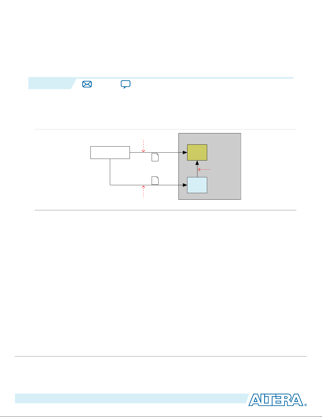
MAX 10 FPGA Configuration Schemes and
CRAM
MAX 10 Device
JTAG In-System Programming
CFM
Configuration Data
Internal
Configuration
JTAG Configuration
.sof
.pof
www.altera.com
101 Innovation Drive, San Jose, CA 95134
Features
2015.05.04
UG-M10CONFIG
Subscribe
Configuration Schemes
Figure 2-1: High-Level Overview of JTAG Configuration and Internal Configuration for MAX 10 Devices
Send Feedback
2
JTAG Configuration
©
2015 Altera Corporation. All rights reserved. ALTERA, ARRIA, CYCLONE, ENPIRION, MAX, MEGACORE, NIOS, QUARTUS and STRATIX words and logos are
trademarks of Altera Corporation and registered in the U.S. Patent and Trademark Office and in other countries. All other words and logos identified as
trademarks or service marks are the property of their respective holders as described at www.altera.com/common/legal.html. Altera warrants performance
of its semiconductor products to current specifications in accordance with Altera's standard warranty, but reserves the right to make changes to any
products and services at any time without notice. Altera assumes no responsibility or liability arising out of the application or use of any information,
product, or service described herein except as expressly agreed to in writing by Altera. Altera customers are advised to obtain the latest version of device
specifications before relying on any published information and before placing orders for products or services.
In MAX 10 devices, JTAG instructions take precedence over the internal configuration scheme.
Using the JTAG configuration scheme, you can directly configure the device CRAM through the JTAG
interface—TDI, TDO, TMS, and TCK pins. The Quartus® II software automatically generates an SRAM
Object File (.sof). You can program the .sof using a download cable with the Quartus II software
programmer.
Related Information
Configuring MAX 10 Devices using JTAG Configuration on page 3-2
Provides more information about JTAG configuration using download cable with Quartus II software
programmer.
ISO
9001:2008
Registered
Page 6

2-2
JTAG Pins
JTAG Pins
Table 2-1: JTAG Pin
Pin Function Description
UG-M10CONFIG
2015.05.04
TDI Serial input pin for:
• instructions
• TDI is sampled on the rising edge of TCK
• TDI pins have internal weak pull-up resistors.
• test data
• programming data
TDO Serial output pin for:
• instructions
• test data
• TDO is sampled on the falling edge of TCK
• The pin is tri-stated if data is not shifted out
of the device.
• programming data
TMS Input pin that provides the control
signal to determine the transitions of
the TAP controller state machine.
TCK Clock input to the BST circuitry. —
All the JTAG pins are powered by the V
1B. In JTAG mode, the I/O pins support the LVTTL/
CCIO
• TMS is sampled on the rising edge of TCK
• TMS pins have internal weak pull-up resistors.
LVCMOS 3.3-1.5V standards.
Related Information
• MAX 10 Device Datasheet
Provides more information about supported I/O standard in MAX 10 devices.
• Guidelines: Dual-Purpose Configuration Pin on page 3-1
• Enabling Dual-purpose Pin on page 3-2
Internal Configuration
You need to program the configuration data into the configuration flash memory (CFM) before internal
configuration can take place. The configuration data to be written to CFM will be part of the programmer
object file (.pof). Using JTAG In-System Programming (ISP), you can program the .pof into the internal
flash.
During internal configuration, MAX 10 devices load the CRAM with configuration data from the CFM.
Internal Configuration Modes
The internal configuration scheme for all MAX 10 devices except for 10M02 device consists of the
following modes:
• Dual Compressed Images—configuration image is stored as image 0 and image 1 in the CFM
• Single Compressed Image
• Single Compressed Image with Memory Initialization
• Single Uncompressed Image
• Single Uncompressed Image with Memory Initialization
In dual compressed images mode, you can use the CONFIG_SEL pin to select the configuration image.
Altera Corporation
MAX 10 FPGA Configuration Schemes and Features
Send Feedback
Page 7

UG-M10CONFIG
2015.05.04
Configuration Flash Memory
The internal configuration scheme for 10M02 device supports the following mode:
• Single Compressed Image
• Single Uncompressed Image
Related Information
• Configuring MAX 10 Devices using Internal Configuration on page 3-4
• Remote System Upgrade in Dual Compressed Images on page 2-8
Configuration Flash Memory
The CFM is a non-volatile internal flash that is used to store configuration images. The CFM may store up
to two compressed configuration images, depending on the compression and the MAX 10 devices. The
compression ratio for the configuration image should be at least 30% for the device to be able store two
configuration images.
Table 2-2: Maximum Number of Compressed Configuration Image for MAX 10 Devices
Device Maximum Number of Compressed Configuration Image
10M02 1
2-3
10M04, 10M08, 10M16, 10M25, 10M40, and 10M50 2
Related Information
Configuration Flash Memory Permissions on page 2-18
Configuration Flash Memory Sectors
All CFM in MAX 10 devices consist of three sectors, CFM0, CFM1, and CFM2 except for the 10M02. The
sectors are programmed differently depending on the internal configuration mode you select.
The 10M02 device consists of only CFM0. The CFM0 sector in 10M02 devices is programmed similarly
when you select single compressed image or single uncompressed image.
MAX 10 FPGA Configuration Schemes and Features
Send Feedback
Altera Corporation
Page 8
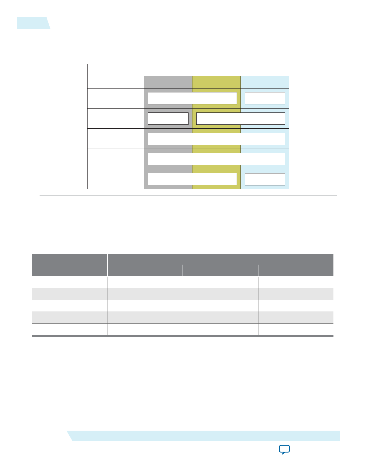
Configuration Flash Memory Sectors
CFM0CFM1CFM2
Dual Compressed Image
Single Uncompressed Image
Single Uncompressed Image
with Memory Initialization
Single Compressed Image
with Memory Initialization
Single Compressed Image
Compressed Image 0
Uncompressed Image 0 with Memory Initialization
Compressed Image 0 with Memory Initialization
Compressed Image 0
Uncompressed Image 0
Compressed Image 1
User Flash Memory
User Flash Memory
Internal Configuration
Mode
2-4
Configuration Flash Memory Total Programming Time
Figure 2-2: Configuration Flash Memory Sectors Utilization for all MAX 10 Devices Except for the
10M02 Device
Unutilized CFM1 and CFM2 sectors can be used for additional user flash memory (UFM).
UG-M10CONFIG
2015.05.04
Configuration Flash Memory Total Programming Time
Table 2-3: Configuration Flash Memory Total Programming Time for Sectors in MAX 10 Devices
10M02 — — 5.4
10M04 6.5 4.6 11.1
10M08 12.0 8.9 20.8
10M16 and 10M25 16.4 12.6 29.0
10M40 and 10M50 30.2 22.7 52.9
In-System Programming
Related Information
CFM and UFM Array Size
Device
CFM2 CFM1 CFM0
You can program the internal flash including the CFM of MAX 10 devices with ISP through industry
standard JTAG interface. ISP offers the capability to program, erase, and verify the CFM. The JTAG
circuitry and ISP instructions for MAX 10 devices are compliant to the IEEE-1532-2002 programming
specification.
Programming Time (s)
During ISP, the MAX 10 receives the IEEE Std. 1532 instructions, addresses, and data through the TDI
input pin. Data is shifted out through the TDO output pin and compared with the expected data.
Altera Corporation
MAX 10 FPGA Configuration Schemes and Features
Send Feedback
Page 9

UG-M10CONFIG
2015.05.04
Real-Time ISP
Real-Time ISP
2-5
The following are the generic flow of an ISP operation:
1. Check ID—the JTAG ID is checked before any program or verify process. The time required to read
this JTAG ID is relatively small compared to the overall programming time.
2. Enter ISP—ensures the I/O pins transition smoothly from user mode to the ISP mode.
3. Sector Erase—shifting in the address and instruction to erase the device and applying erase pulses.
4. Program—shifting in the address, data, and program instructions and generating the program pulse to
program the flash cells. This process is repeated for each address in the internal flash sector.
5. Verify—shifting in addresses, applying the verify instruction to generate the read pulse, and shifting
out the data for comparison. This process is repeated for each internal flash address.
6. Exit ISP—ensures that the I/O pins transition smoothly from the ISP mode to the user mode.
You can also use the Quartus II Programmer to program the CFM.
Related Information
Programming .pof into Internal Flash on page 3-7
Provides the steps to program the .pof using Quartus II Programmer.
In a normal ISP operation, to update the internal flash with a new design image, the device exits from user
mode and all I/O pins remain tri-stated. After the device completes programing the new design image, it
resets and enters user mode.
The real-time ISP feature updates the internal flash with a new design image while operating in user
mode. During the internal flash programming, the device continues to operate using the existing design.
After the new design image programming process completes, the device will not reset. The new design
image update only takes effect in the next reconfiguration cycle.
ISP and Real-Time ISP Instructions
Table 2-4: ISP and Real-Time ISP Instructions for MAX 10 Devices
Instruction Instruction Code Description
CONFIG_IO 00 0000 1101
• Allows I/O reconfiguration through JTAG ports using
the IOCSR for JTAG testing. This is executed after or
during configurations.
• nSTATUS pin must go high before you can issue the
CONFIG_IO instruction.
PULSE_NCONFIG 00 0000 0001 Emulates pulsing the nCONFIG pin low to trigger reconfi‐
guration even though the physical pin is unaffected.
MAX 10 FPGA Configuration Schemes and Features
Send Feedback
Altera Corporation
Page 10

2-6
ISP and Real-Time ISP Instructions
Instruction Instruction Code Description
ISC_ENABLE_HIZ
(1)
10 1100 1100
UG-M10CONFIG
2015.05.04
• Puts the device in ISP mode, tri-states all I/O pins,
and drives all core drivers, logic, and registers.
• Device remains in the ISP mode until the ISC_
DISABLE instruction is loaded and updated.
• The ISC_ENABLE instruction is a mandatory instruc‐
tion. This requirement is met by the ISC_ENABLE_
CLAMP or ISC_ENABLE_HIZ instruction.
ISC_ENABLE_CLAMP
ISC_DISABLE 10 0000 0001
ISC_PROGRAM
ISC_NOOP
(2)
(2)
(1)
10 0011 0011
10 1111 0100 Sets the device up for in-system programming. Program‐
10 0001 0000
• Puts the device in ISP mode and forces all I/O pins to
follow the contents of the JTAG boundary-scan
register.
• When this instruction is activated, all core drivers,
logics, and registers are frozen. The I/O pins remain
clamped until the device exits ISP mode successfully.
• Brings the device out of ISP mode.
• Successful completion of the ISC_DISABLE instruction
happens immediately after waiting 200 µs in the RunTest/Idle state.
ming occurs in the run-test or idle state.
• Sets the device to a no-operation mode without
leaving the ISP mode and targets the ISC_Default
register.
• Use when:
• two or more ISP-compliant devices are being
accessed in ISP mode and;
• a subset of the devices perform some instructions
while other more complex devices are completing
extra steps in a given process.
ISC_ADDRESS_SHIFT
ISC_ERASE
ISC_READ
(1)
Do not issue the ISC_ENABLE_HIZ and ISC_ENABLE_CLAMP instructions from the core logic.
(2)
All ISP and real-time ISP instructions are disabled when the device is not in the ISP or real-time ISP mode,
except for the enabling and disabling instructions.
Altera Corporation
(2)
(2)
(2)
10 0000 0011 Sets the device up to load the flash address. It targets the
ISC_Address register, which is the flash address register.
10 1111 0010
• Sets the device up to erase the internal flash.
• Issue after ISC_ADDRESS_SHIFT instruction.
10 0000 0101
• Sets the device up for verifying the internal flash
under normal user bias conditions.
• The ISC_READ instruction supports explicit
addressing and auto-increment, also known as the
Burst mode.
MAX 10 FPGA Configuration Schemes and Features
Send Feedback
Page 11

UG-M10CONFIG
2015.05.04
Initialization Configuration Bits
Instruction Instruction Code Description
2-7
BGP_ENABLE 01 1001 1001
• Sets the device to the real-time ISP mode.
• Allows access to the internal flash configuration
sector while the device is still in user mode.
BGP_DISABLE 01 0110 0110
• Brings the device out of the real-time ISP mode.
• The device has to exit the real-time ISP mode using
the BGP_DISABLE instruction after it is interrupted by
reconfiguration.
Caution: Do not use unsupported JTAG instructions. It will put the device into an unknown state and
requires a power cycle to recover the operation.
Initialization Configuration Bits
Initialization Configuration Bits (ICB) stores the configuration feature settings of the MAX 10 device. You
can set the ICB settings during Convert Programming File.
Table 2-5: Initialization Configuration Bits for MAX 10 Devices
Configuration Settings Description Default State/Value
Power On Reset Scheme
• Instant ON
• Fast POR delay
• Slow POR delay
Instant ON
Set I/O to weak pull-up prior
usermode
Auto-reconfigure from
secondary image when initial
image fails.
Use secondary image ISP data
as default setting when
available.
• Enable: I/O will set to week pull-up prior to
usermode.
• Disable: I/O will be input tri-stated.
Enable:
• Device will automatically load secondary image
if initial image fails.
Disable:
• device will automatically load image 0.
• device will not load image 1 if image 0 fails.
• CONFIG_SEL pin setting is ignored.
• Disable: Use ISP data from image 0
• Enable: Use ISP data from image 1
ISP data contains the information about state of
the pin during ISP. This can be either tri-state with
weak pull-up or clamp the I/O state. You can set
the ISP clamp through Device and Pin Option, or
Pin Assignment tool.
Enable
Enable
Disable
Verify Protect To disable or enable the Verify Protect feature. Disable
MAX 10 FPGA Configuration Schemes and Features
Send Feedback
Altera Corporation
Page 12

2-8
Configuration Features
Configuration Settings Description Default State/Value
UG-M10CONFIG
2015.05.04
Allow encrypted POF only If enabled, configuration error will occur if
unencrypted .pof is used.
JTAG Secure
(3)
To disable or enable the JTAG Secure feature. Disable
Enable Watchdog To disable or enable the watchdog timer for
remote system upgrade.
Watchdog value To set the watchdog timer value for remote system
upgrade.
Related Information
• .pof and ICB Settings on page 3-5
• .pof Generation through Convert Programming Files on page 3-6
Provides more information about setting the ICB during .pof generation using Convert Programming
File.
• Instant-on on page 2-24
Provides more information about Instant ON and other power on reset scheme.
• Verify Protect on page 2-17
• JTAG Secure Mode on page 2-16
• ISP and Real-Time ISP Instructions on page 2-5
• User Watchdog Timer on page 2-14
Disable
Enable
0x1FFF
(4)
Configuration Features
Remote System Upgrade in Dual Compressed Images
MAX 10 devices support the remote system upgrade feature. By default, the remote system upgrade
feature is enabled in all MAX 10 devices when you select the dual compressed image internal
configuration mode.
The remote system upgrade feature in MAX 10 devices offers the following capabilities:
• Manages remote configuration
• Provides error detection, recovery, and information
• Supports direct-to-application configuration image
• Supports compressed and encrypted .pof
You can use the Altera Dual Configuration IP core or the remote system upgrade circuitry to access the
remote system upgrade block in MAX 10 devices.
(3)
The JTAG Secure feature will be disabled by default in Quartus II. If you are interested in using the JTAG
Secure feature, contact Altera for support.
(4)
The watchdog timer value depends on the MAX 10 you are using. Refer to the Watchdog Timer section for
more information.
Altera Corporation
MAX 10 FPGA Configuration Schemes and Features
Send Feedback
Page 13
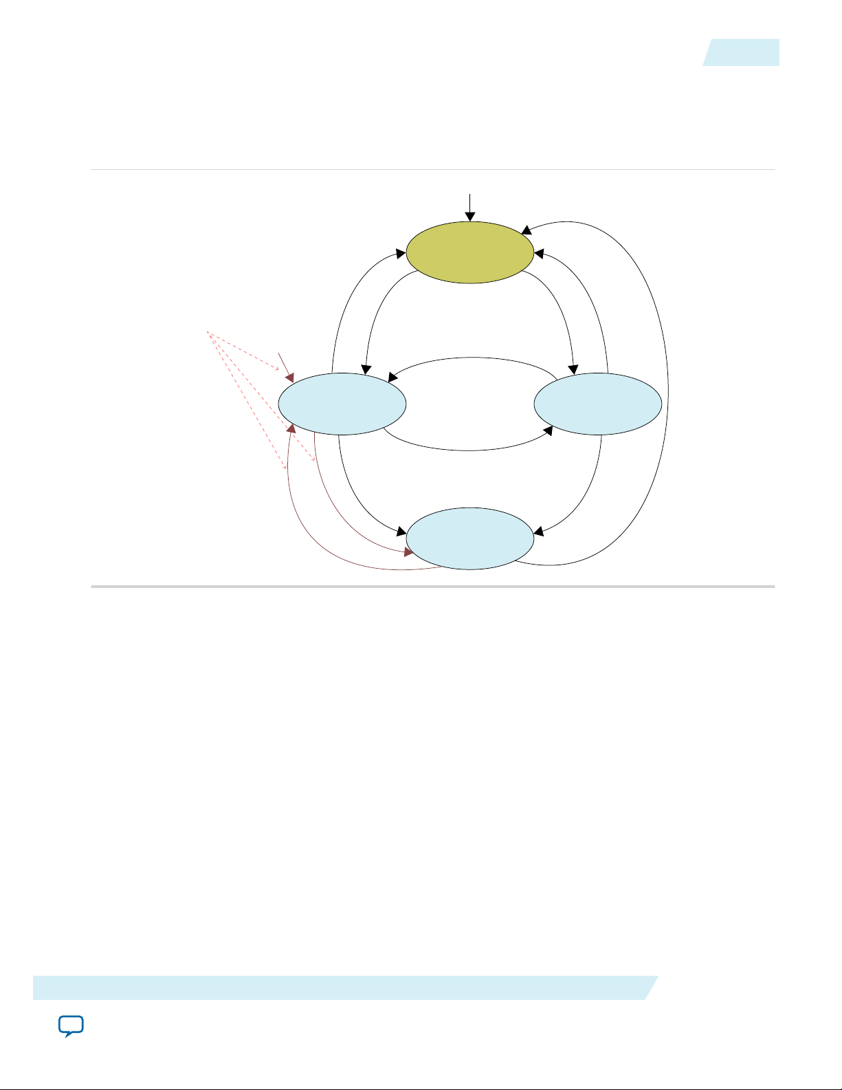
Sample CONFIG_SEL pin
Image 0 Image 1
CONFIG_SEL=0
CONFIG_SEL=1
Wait for Reconfiguration
Power-up
Reconfiguration
Reconfiguration
Reconfiguration
First Error Occurs
First Error Occurs
Second Error Occurs
Flow when Auto-reconfigure
from secondary image when
initial image fails is disabled.
Second Error Occurs
Power-up
Error Occurs
Reconfiguration
UG-M10CONFIG
2015.05.04
Remote System Upgrade Flow
Both the application configuration images, image 0 and image 1, are stored in the CFM. The MAX 10
device loads either one of the application configuration image from the CFM.
Figure 2-3: Remote System Upgrade Flow for MAX 10 Devices
Remote System Upgrade Flow
2-9
MAX 10 FPGA Configuration Schemes and Features
The remote system upgrade feature detects errors in the following sequence:
1. After power-up, the device samples the CONFIG_SEL pin to determine which application configuration
image to load. The CONFIG_SEL pin setting can be overwritten by the input register of the remote
system upgrade circuitry for the subsequent reconfiguration.
2. If an error occurs, the remote system upgrade feature reverts by loading the other application configu‐
ration image. These errors cause the remote system upgrade feature to load another application
configuration image:
• Internal CRC error
• User watchdog timer time-out
3. Once the revert configuration completes and the device is in user mode, you can use the remote system
upgrade circuitry to query the cause of error and which application image failed.
4. If a second error occurs, the device waits for a reconfiguration source. If the Auto-restart configura‐
tion after error is enabled, the device will reconfigure without waiting for any reconfiguration source.
5. Reconfiguration is triggered by the following actions:
• Driving the nSTATUS low externally.
• Driving the nCONFIG low externally.
• Driving RU_nCONFIG low.
Altera Corporation
Send Feedback
Page 14
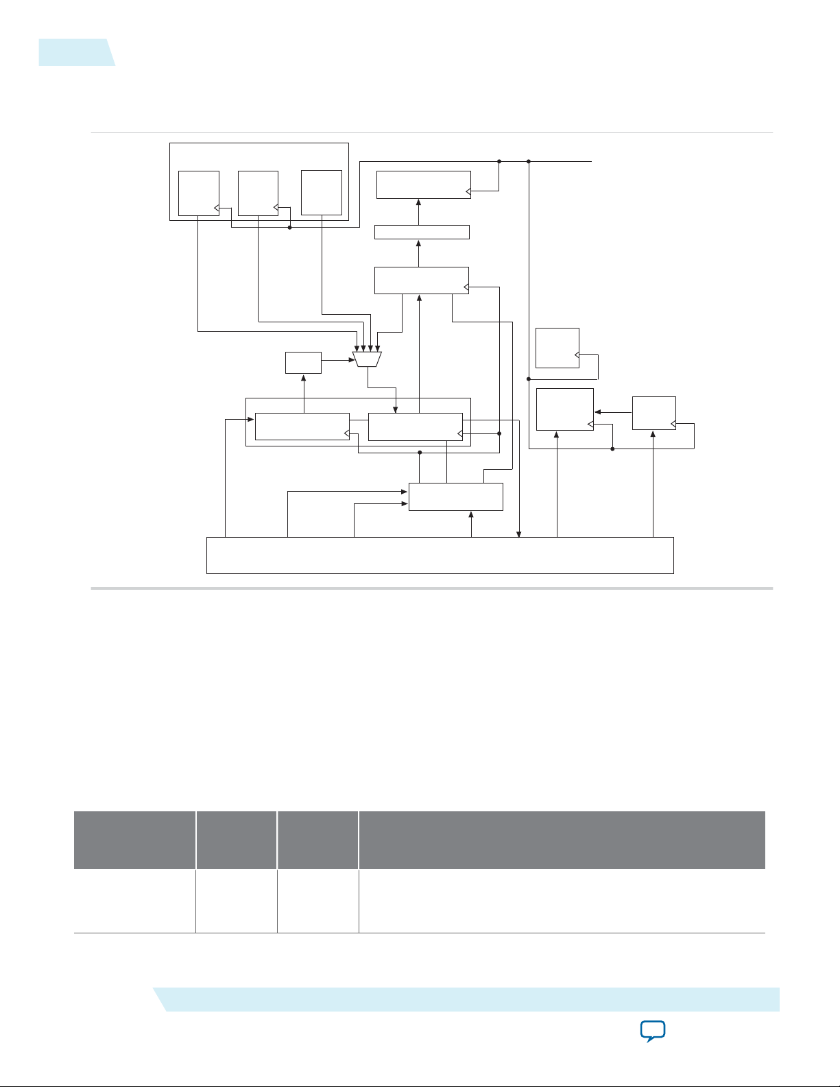
Status Register (SR)
Previous
State
Register 2
Bit[31..0]
State
Register 1
Bit[31..0]
Current
State
Logic
Bit[33..0]
Internal Oscillator
Control Register
Bit [38..0]
Logic
Input Register
Bit [38..0]
update
Logic
Bit [40..39]
doutdin
Bit [38..0]
dout
din
capture
Shift Register
clkout
capture
update
Logic
clkin
RU_DIN
RU_SHIFTnLD
RU_CAPTnUPDT
RU_CLK
RU_nRSTIMER
Logic Array
RU
Reconfiguration
State
Machine
User
Watchdog
Timer
RU
Master
State
Machine
timeout
RU_nCONFIGRU_DOUT
Previous
2-10
Remote System Upgrade Circuitry
Remote System Upgrade Circuitry
Figure 2-4: Remote System Upgrade Circuitry
UG-M10CONFIG
2015.05.04
Table 2-6: Remote System Upgrade Circuitry Signals for MAX 10 Devices
Altera Corporation
The remote system upgrade circuitry does the following functions:
• Tracks the current state of configuration
• Monitors all reconfiguration sources
• Provides access to set up the application configuration image
• Returns the device to fallback configuration if an error occurs
• Provides access to the information on the failed application configuration image
Remote System Upgrade Circuitry Signals
Core Signal Name Logical
Signal
Name
RU_DIN regin Input
Input/
Output
Description
Use this signal to write data to the shift register on the rising
edge of RU_CLK. To load data to the shift register, assert RU_
SHIFTnLD.
MAX 10 FPGA Configuration Schemes and Features
Send Feedback
Page 15

UG-M10CONFIG
2015.05.04
Remote System Upgrade Circuitry Input Control
2-11
Core Signal Name Logical
Signal
Name
Input/
Output
Description
Use this signal to get output data from the shift register. Data
RU_DOUT regout Output
is clocked out on each rising edge of RU_CLK if RU_SHIFTnLD is
asserted.
RU_nRSTIMER rsttimer Input
Use this signal to reset the user watchdog timer. A falling edge
of this signal triggers a reset of the user watchdog timer.
Use this signal to reconfigure the device. Driving this signal
RU_nCONFIG rconfig Input
low triggers the device to reconfigure if you enable the remote
system upgrade feature.
The clock to the remote system upgrade circuitry. All registers
RU_CLK clk Input
in this clock domain are enabled in user mode if you enable
the remote system upgrade. Shift register and input register
are positive edge flip-flops.
RU_SHIFTnLD shiftnld Input Control signals that determine the mode of remote system
upgrade circuitry.
• When RU_SHIFTnLD is driven low and RU_CAPTnUPDT is
driven low, the input register is loaded with the contents of
the shift register on the rising edge of RU_CLK.
• When RU_SHIFTnLD is driven low and RU_CAPTnUPDT is
RU_CAPTnUPDT captnupdt Input
driven high, the shift register captures values from the
input_cs_ps module on the rising edge of RU_CLK.
• When RU_SHIFTnLD is driven high, the RU_CAPTnUPDT will
be ignored and the shift register shifts data on each rising
edge of RU_CLK.
Related Information
• Accessing the Remote System Upgrade Block Through User Interface on page 3-8
Provides more information about accessing the remote system upgrade through user interface atom.
• MAX 10 Device Datasheet
Provides more information about Remote System Upgrade timing specifications.
Remote System Upgrade Circuitry Input Control
The remote system upgrade circuitry has three modes of operation.
• Update—loads the values in the shift register into the input register.
• Capture—loads the shift register with data to be shifted out.
• Shift—shifts out data to the user logic.
MAX 10 FPGA Configuration Schemes and Features
Send Feedback
Altera Corporation
Page 16

2-12
Remote System Upgrade Input Register
Table 2-7: Control Inputs to the Remote System Upgrade Circuitry
UG-M10CONFIG
2015.05.04
Remote System Upgrade Circuitry Control Inputs
RU_SHIFTnLD RU_CAPTnUPDT Shift register
[40]
Shift register
[39]
Operation
Mode
0 0 Don't Care Don't Care Update
0 1 0 0 Capture Current State
0 1 0 1 Capture
Previous State
Application1}
0 1 1 0 Capture
Previous State
Application2}
0 1 1 1 Capture
Register[38:0]
1 Don't Care Don't Care Don't Care Shift
Input Settings for Registers
Shift
Register[38:0]
Shift Register
[38:0]
Input
Register[38:0]
Shift Register
[38:0]
Input
Register[38:0]
{8’b0,
Input
Register[38:0]
{8’b0,
Input
Register[38:0]
Input
Input
Register[38:0]
{ru_din, Shift
Register
[38:1]}
Input
Register[38:0]
The following shows examples of driving the control inputs in the remote system upgrade circuitry:
• When you drive RU_SHIFTnLD high to 1’b1, the shift register shifts data on each rising edge of RU_CLK
and RU_CAPTnUPDT has no function.
• When you drive both RU_SHIFTnLD and RU_CAPTnUPDT low to 1’b0, the input register is loaded with
the contents of the shift register on the rising edge of RU_CLK.
• When you drive RU_SHIFTnLD low to 1’b0 and RU_CAPTnUPDT high to 1’b1, the shift register
captures values on the rising edge of RU_DCLK.
Remote System Upgrade Input Register
Table 2-8: Remote System Upgrade Input Register for MAX 10 Devices
Bits Name Description
38:14 Reserved Reserved—set to 0.
• 0: Load configuration image 0
13 ru_config_sel
• 1: Load configuration image 1
This bit will only work if the ru_config_sel_overwrite bit is set
to 1.
12
ru_config_sel_
overwrite
• 0: Disable overwrite CONFIG_SEL pin
• 1: Enable overwrite CONFIG_SEL pin
Altera Corporation
MAX 10 FPGA Configuration Schemes and Features
Send Feedback
Page 17

UG-M10CONFIG
2015.05.04
Bits Name Description
Remote System Upgrade Status Registers
11:0 Reserved Reserved—set to 0.
Remote System Upgrade Status Registers
Table 2-9: Remote System Upgrade Status Register—Current State Logic Bit for MAX 10 Devices
Bits Name Description
33:30 msm_cs The current state of the master state machine (MSM).
2-13
29 ru_wd_en
The current state of the enabled user watchdog timer. The default
state is active high.
28:0 wd_timeout_value The current, entire 29-bit watchdog time-out value.
Table 2-10: Remote System Upgrade Status Register—Previous State Bit for MAX 10 Devices
Bits Name Description
31 nconfig An active high field that describes the reconfiguration sources
30 crcerror
29 nstatus
which caused the MAX 10 device to leave the previous application
configuration. In the event of a tie, the higher bit order takes
precedence. For example, if the nconfig and the ru_nconfig
triggered at the same time, the nconfig takes precedence over the
28 wdtimer
ru_nconfig.
27:26 Reserved Reserved—set to 0.
The state of the MSM when a reconfiguration event occurred. The
25:22 msm_cs
reconfiguration will cause the device to leave the previous applica‐
tion configuration.
21:0 Reserved Reserved—set to 0.
Master State Machine
The master state machine (MSM) tracks current configuration mode and enables the user watchdog
timer.
Table 2-11: Remote System Upgrade Master State Machine Current State Descriptions for MAX 10 Devices
msm_cs Values State Description
0010 Image 0 is being loaded.
0011 Image 1 is being loaded after a revert in application image happens.
0100 Image 1 is being loaded.
0101 Image 0 is being loaded after a revert in application image happens.
MAX 10 FPGA Configuration Schemes and Features
Send Feedback
Altera Corporation
Page 18

Altera
Dual Configuration
clk
nreset
avmm_rcv_address[2..0]
avmm_rcv_read
avmm_rcv_writedata[31..0]
avmm_rcv_write
avmm_rcv_readdata[31..0]
2-14
User Watchdog Timer
User Watchdog Timer
The user watchdog timer prevents a faulty application configuration from stalling the device indefinitely.
You can use the timer to detect functional errors when an application configuration is successfully loaded
into the device.
The counter is 29 bits wide and has a maximum count value of 229. When specifying the user watchdog
timer value, specify only the most significant 12 bits. The granularity of the timer setting is 217 cycles. The
cycle time is based on the frequency of the user watchdog timer internal oscillator. Depending on the
counter and the internal oscillator of the device, you can set the cycle time from 9ms to 244s.
Figure 2-5: Watchdog Timer Formula for MAX 10 Devices
The timer begins counting as soon as the application configuration enters user mode. When the timer
expires, the remote system upgrade circuitry generates a time-out signal, updates the status register, and
triggers the loading of the revert configuration image. To reset the timer, pulse the RU_NRSTIMER for a
minimum of 250 ns.
UG-M10CONFIG
2015.05.04
When you enable the watchdog timer, the setting will apply to all images, all images should contain the
soft logic configuration to reset the timer. Application Configuration will reset the control block registers.
Related Information
• User Watchdog Internal Circuitry Timing Specifications
Provides more information about the user watchdog frequency.
• Initialization Configuration Bits on page 2-7
Altera Dual Configuration IP Core
The Altera Dual Configuration IP core offers the following capabilities through Avalon-MM interface:
• Asserts RU_nCONFIG to trigger reconfiguration.
• Asserts RU_nRSTIMER to reset watchdog timer if the watchdog timer is enabled.
• Writes configuration setting to the input register of the remote system upgrade circuitry.
• Reads information from the remote system upgrade circuitry.
Figure 2-6: Altera Dual Configuration IP Core Block Diagram
Altera Corporation
MAX 10 FPGA Configuration Schemes and Features
Send Feedback
Page 19

UG-M10CONFIG
2015.05.04
Related Information
• Altera Dual Configuration IP Core Avalon-MM Address Map on page 5-1
• Avalon Interface Specifications
Provides more information about the Avalon-MM interface specifications applied in Altera Dual
Configuration IP Core.
• Instantiating the Altera Dual Configuration IP Core on page 4-2
• Accessing the Remote System Upgrade Block Through User Interface on page 3-8
Configuration Design Security
The MAX 10 design security feature supports the following capabilities:
• Encryption—Built-in encryption standard (AES) to support 128-bit key industry-standard design
security algorithm
• Chip ID—Unique device identification
• JTAG secure mode—limits access to JTAG instructions
• Verify Protect—allows optional disabling of CFM content read-back
AES Encryption Protection
The MAX 10 design security feature provides the following security protection for your designs:
Configuration Design Security
2-15
• Security against copying—the non-volatile key is securely stored in the MAX 10 devices and cannot be
read through any interface. Without this key, attacker will not be able to decrypt the encrypted
configuration image.
• Security against reverse engineering—reverse engineering from an encrypted configuration file is very
difficult and time consuming because the file require decryption.
• Security against tampering—after you enable the JTAG Secure and Encrypted POF (EPOF) only, the
MAX 10 device can only accept configuration files encrypted with the same key. Additionally, configu‐
ration through the JTAG interface is blocked.
Related Information
.pof Generation through Convert Programming Files on page 3-6
Encryption and Decryption
MAX 10 supports AES encryption. Programming bitstream is encrypted based on the encryption key that
is specified by user. In MAX 10 devices, the key is part of the ICB settings stored in the internal flash.
Hence, the key will be non-volatile but user can clear/delete the key by a full chip erase the device.
When you use compression with encryption, the configuration file is first compressed, and then
encrypted using the Quartus II software. During configuration, the device first decrypts, and then
decompresses the configuration file.
The header and I/O configuration shift register (IOCSR) data will not be encrypted. The decryption block
is activated after the IOCSR chain is programmed. The decryption block only decrypts core data and
postamble.
Related Information
JTAG Instruction Availability on page 2-17
MAX 10 FPGA Configuration Schemes and Features
Send Feedback
Altera Corporation
Page 20

Altera Unique
Chip ID
clkin data_valid
chip_id[63..0]reset
2-16
Unique Chip ID
Unique Chip ID
Unique chip ID provides the following features:
• Identifies your device in your design as part of a security feature to protect your design from an
unauthorized device.
• Provides non-volatile 64-bits unique ID for each MAX 10 device with write protection.
You can use the Altera Unique Chip ID IP core to acquire the chip ID of your MAX 10 device.
Related Information
• Altera Unique Chip ID IP Core on page 4-1
• Altera Unique Chip ID IP Core Ports on page 6-1
Altera Unique Chip ID IP Core
Figure 2-7: Altera Unique Chip ID IP Core Block Diagram
UG-M10CONFIG
2015.05.04
At the initial state, the data_valid signal is low because no data is read from the unique chip ID block.
After feeding a clock signal to the clkin input port, the Altera Unique Chip ID IP core begins to acquire
the chip ID of your device through the unique chip ID block. After acquiring the chip ID of your device,
the Altera Unique Chip ID IP core asserts the data_valid signal to indicate that the chip ID value at the
output port is ready for retrieval.
The operation repeats only when you provide another clock signal when the data_valid signal is low. If
the data_valid signal is high when you provide another clock signal, the operation stops because the
chip_id[63..0] output holds the chip ID of your device.
A minimum of 67 clock cycles are required for the data_valid signal to go high.
The chip_id[63:0]output port holds the value of chip ID of your device until you reconfigure the device
or reset the Altera Unique Chip ID IP core.
JTAG Secure Mode
In JTAG Secure mode, the device only allows mandatory JTAG 1149.1 instructions to be exercised.
You can enable the JTAG secure when generating the .pof in the Convert Programming Files. To exit JTAG
secure mode, issue the UNLOCK JTAG instruction. The LOCK JTAG instruction puts the device in the JTAG
secure mode again. The LOCK and UNLOCK JTAG instructions can only be issued through the JTAG core
access.
Altera Corporation
MAX 10 FPGA Configuration Schemes and Features
Send Feedback
Page 21

UG-M10CONFIG
2015.05.04
Related Information
• JTAG Instruction Availability on page 2-17
• Configuration Flash Memory Permissions on page 2-18
• .pof Generation through Convert Programming Files on page 3-6
JTAG Secure Mode Instructions
Table 2-12: JTAG Secure Mode Instructions for MAX 10 Devices
JTAG Instruction Instruction Code Description
JTAG Secure Mode Instructions
2-17
LOCK 10 0000 0010
• Activates the JTAG secure mode.
• Blocks access from both external pins and core to
JTAG.
UNLOCK 10 0000 1000 Deactivates the JTAG secure mode.
Verify Protect
Verify Protect is a security feature to enhance CFM security. When you enable the Verify Protect, only
program and erase operation are allowed on the CFM. This capability protects the CFM contents from
being copied.
You can turn on the Verify Protect feature by enabling the Verify Protect in the Quartus II programmer.
Related Information
Configuration Flash Memory Permissions on page 2-18
JTAG Instruction Availability
Table 2-13: JTAG Instruction Availability Based on JTAG Secure Mode and Encryption Settings
JTAG Secure Mode Encryption Description
Disabled All JTAG Instructions enabled
Disabled
Enabled
Disabled All JTAG Instructions are disabled except:
Enabled
Enabled
Related Information
• JTAG Secure Mode on page 2-16
MAX 10 FPGA Configuration Schemes and Features
Send Feedback
All JTAG Instructions are enabled except:
• CONFIGURE
• SAMPLE/PRELOAD
• BYPASS
• EXTEST
• IDCODE
• UNLOCK
• LOCK
Altera Corporation
Page 22

2-18
Configuration Flash Memory Permissions
• Encryption and Decryption on page 2-15
Configuration Flash Memory Permissions
The JTAG secure mode and verify protect features determines the CFM operation permission.. The table
list the operations permitted based on the security settings.
Table 2-14: CFM Permissions for MAX 10 Devices
JTAG Secure Mode Disabled JTAG Secure Mode Enabled
Operation
ISP through core Illegal operation Illegal operation Illegal operation Illegal operation
Verify Protect
Disabled
Verify Protect
Enabled
Verify Protect
Disabled
UG-M10CONFIG
2015.05.04
Verify Protect
Enabled
ISP through
JTAG pins
Real-time ISP
through core
Real-time ISP
through JTAG
pins
UFM interface
through core
Related Information
(5)
Full access
Full access
Full access
Full access Full access Full access Full access
Program and erase
only
Program and erase
only
Program and erase
only
• JTAG Secure Mode on page 2-16
• Verify Protect on page 2-17
SEU Mitigation and Configuration Error Detection
The dedicated circuitry built in MAX 10 devices consists of an error detection cyclic redundancy check
(EDCRC) feature. You can use this feature to mitigate single-event upset (SEU) or soft errors.
The hardened on-chip EDCRC circuitry allows you to perform the following operations without any
impact on the fitting of the device:
No access No access
No access No access
No access No access
• Auto-detection of cyclic redundancy check (CRC) errors during configuration.
• Identification of SEU in user mode with the optional CRC error detection.
• Testing of error detection by error detection verification through the JTAG interface.
Related Information
• Verifying Error Detection Functionality on page 3-8
• Enabling Error Detection on page 3-9
• Accessing Error Detection Block Through User Interface on page 3-9
(5)
The UFM interface through core is available if you select the dual compressed image mode.
Altera Corporation
MAX 10 FPGA Configuration Schemes and Features
Send Feedback
Page 23

Control Signals
Error Detection
State Machine
32-bit Storage
Register
Compute & Compare
CRC
32-bit Signature
Register
32
32
32
CRC_ERROR
UG-M10CONFIG
2015.05.04
Configuration Error Detection
In configuration mode, a frame-based CRC is stored in the configuration data and contains the CRC value
for each data frame.
During configuration, the MAX 10 device calculates the CRC value based on the frame of data that is
received and compares it against the frame CRC value in the data stream. Configuration continues until
the device detects an error or when all the values are calculated.
For MAX 10 devices, the CRC is computed by the Quartus II software and downloaded into the device as
part of the configuration bit stream. These devices store the CRC in the 32-bit storage register at the end
of the configuration mode.
User Mode Error Detection
SEUs are changes in a CRAM bit state due to an ionizing particle. MAX 10 devices have built-in error
detection circuitry to detect data corruption in the CRAM cells.
This error detection capability continuously computes the CRC of the configured CRAM bits. The CRC of
the contents of the device are compared with the pre-calculated CRC value obtained at the end of the
configuration. If the CRC values match, there is no error in the current configuration CRAM bits. The
process of error detection continues until the device is reset—by setting nCONFIG to low.
The error detection circuitry in MAX 10 device uses a 32-bit CRC IEEE Std. 802 and a 32-bit polynomial
as the CRC generator. Therefore, the device performs a single 32-bit CRC calculation. If an SEU does not
occur, the resulting 32-bit signature value is 0x000000, which results in a 0 on the output signal
CRC_ERROR. If an SEU occurs in the device, the resulting signature value is non-zero and the CRC_ERROR
output signal is 1. You must decide whether to reconfigure the FPGA by strobing the nCONFIG pin low or
ignore the error.
Configuration Error Detection
2-19
Error Detection Block
Figure 2-8: Error Detection Block Diagram
Error detection block diagram including the two related 32-bit registers—the signature register and the
storage register.
There are two sets of 32-bit registers in the error detection circuitry that store the computed CRC
signature and pre-calculated CRC value. A non-zero value on the signature register causes the CRC_ERROR
pin to go high.
MAX 10 FPGA Configuration Schemes and Features
Send Feedback
Altera Corporation
Page 24

2-20
CHANGE_EDREG JTAG Instruction
Table 2-15: Error Detection Registers for MAX 10 Devices
Register Description
This register contains the CRC signature. The signature register contains the
result of the user mode calculated CRC value compared against the pre-
32-bit signature register
calculated CRC value. If no errors are detected, the signature register is all
zeroes. A non-zero signature register indicates an error in the configuration
CRAM contents. The CRC_ERROR signal is derived from the contents of this
register.
This register is loaded with the 32-bit pre-computed CRC signature at the end
of the configuration stage. The signature is then loaded into the 32-bit
Compute and Compare CRC block during user mode to calculate the CRC
error. This register forms a 32-bit scan chain during execution of the CHANGE_
32-bit storage register
EDREG JTAG instruction. The CHANGE_EDREG JTAG instruction can change the
content of the storage register. Therefore, the functionality of the error
detection CRC circuitry is checked in-system by executing the instruction to
inject an error during the operation. The operation of the device is not halted
when issuing the CHANGE_EDREG JTAG instruction.
CHANGE_EDREG JTAG Instruction
UG-M10CONFIG
2015.05.04
Table 2-16: CHANGE_EDREG JTAG Instruction Description
JTAG Instruction Instruction Code Description
CHANGE_EDREG 00 0001 0101 This instruction connects the 32-bit CRC storage register
between TDI and TDO. Any precomputed CRC is loaded
into the CRC storage register to test the operation of the
error detection CRC circuitry at the CRC_ERROR pin.
Error Detection Timing
When the error detection CRC feature is enabled through the Quartus II software, the device
automatically activates the CRC process upon entering user mode, after configuration and initialization is
complete.
The CRC_ERROR pin will remain low until the error detection circuitry has detected a corrupted bit in the
previous CRC calculation. After the pin goes high, it remains high during the next CRC calculation. This
pin does not log the previous CRC calculation. If the new CRC calculation does not contain any corrupted
bits, the CRC_ERROR pin is driven low. The error detection runs until the device is reset.
The error detection circuitry is clocked by an internal configuration oscillator with a divisor that sets the
maximum frequency. The CRC calculation time depends on the device and the error detection clock
frequency.
Related Information
Enabling Error Detection on page 3-9
Error Detection Frequency
You can set a lower clock frequency by specifying a division factor in the Quartus II software.
Altera Corporation
MAX 10 FPGA Configuration Schemes and Features
Send Feedback
Page 25

UG-M10CONFIG
2015.05.04
Cyclic Redundancy Check Calculation Timing
Table 2-17: Minimum and Maximum Error Detection Frequencies for MAX 10 Devices—Preliminary
2-21
Device Error Detection Frequency Maximum Error
Detection
Frequency (MHz)
Minimum Error
Detection
Frequency (kHz)
10M02
10M04
10M08
55 MHz/2n to 116 MHz/2
n
58 214.8
10M16
10M25
10M40
35 MHz/2n to 77 MHz/2
n
38.5 136.7
10M50
Cyclic Redundancy Check Calculation Timing
Table 2-18: Cyclic Redundancy Check Calculation Time for MAX 10 Devices—Preliminary
Device
Minimum Time (ms) Maximum Time (ms)
Divisor Value (n = 2)
10M02 2 6.6
Valid Values for n
2, 3, 4, 5, 6, 7, 8
10M04 6 15.7
10M08 6 15.7
10M16 10 25.5
10M25 14 34.7
10M40 43 106.7
10M50 43 106.7
Figure 2-9: CRC Calculation Formula
You can use this formula to calculate the CRC calculation time for divisor other than 2.
Example 2-1: CRC Calcualtion Example
For 10M16 device with divisor value of 256:
Minimum CRC calculation time for divisor 256 = 10 x (256/2) = 1280 ms
MAX 10 FPGA Configuration Schemes and Features
Send Feedback
Altera Corporation
Page 26

2-22
Recovering from CRC Errors
Recovering from CRC Errors
The system that MAX 10 resides in must control device reconfiguration. After detecting an error on the
CRC_ERROR pin, strobing the nCONFIG pin low directs the system to perform reconfiguration at a time
when it is safe for the system to reconfigure the MAX 10 device.
When the data bit is rewritten with the correct value by reconfiguring the device, the device functions
correctly.
While SEUs are uncommon in Altera devices, certain high-reliability applications might require a design
to account for these errors.
Configuration Data Compression
MAX 10 devices can receive compressed configuration bitstream and decompress the data in real-time
during configuration. This feature helps to reduce the configuration image size stored in the CFM.
Preliminary data indicates that compression typically reduces the configuration file size by at least 30%
depending on the design.
Related Information
• Enabling Compression Before Design Compilation on page 3-11
• Enabling Compression After Design Compilation on page 3-11
UG-M10CONFIG
2015.05.04
Altera Corporation
MAX 10 FPGA Configuration Schemes and Features
Send Feedback
Page 27

Power supplies including V
CCIO
, V
CCA
and V
CC
reach recommended operating voltage
nSTATUS and nCONFIG released high
CONF_DONE pulled low
CONF_DONE released high
Power Up
•
nSTATUS and CONF_DONE
driven low
• All I/Os pins are tri-stated
• Clears configuration RAM bits
Reset
• nSTATUS and CONF_DONE remain low
Initialization
• Initializes internal logic and
registers
• Enables I/O buffers
Configuration Error Handling
• nSTATUS pulled low
• CONF_DONE remains low
• Restarts configuration if option
enabled
User Mode
Executes your design
Configuration
Writes configuration data to
FPGA
• All I/Os pins are tri-stated
• Samples CONFIG_SEL pin
UG-M10CONFIG
2015.05.04
Configuration Details
Configuration Sequence
Figure 2-10: Configuration Sequence for MAX 10 Devices
Configuration Details
2-23
You can initiate reconfiguration by pulling the nCONFIG pin low to at least the minimum t
width. When this pin is pulled low, the nSTATUS and CONF_DONE pins are pulled low and all I/O pins are
tied to an internal weak pull-up.
MAX 10 FPGA Configuration Schemes and Features
Send Feedback
low-pulse
CFG
Altera Corporation
Page 28

2-24
Power Up
Power Up
Related Information
.pof Generation through Convert Programming Files on page 3-6
Provides more information about how to set th weak pull-up during configuration.
UG-M10CONFIG
2015.05.04
If you power-up a device from the power-down state, you need to power the V
CCIO
the appropriate level for the device to exit POR.
To begin configuration, the required voltages must be powered up to the appropriate voltage levels as
shown in the following table. The V
for bank 1B and bank 8 must be powered up to a voltage between
CCIO
1.5V – 3.3V during configuration.
Table 2-19: Single-Supply and Dual-Supply Voltage Requirements for MAX 10 Devices
Power Supply Device Options Voltage that must be Powered-Up
Single-supply
Dual-supply
Related Information
Regulated V
V
bank 1B and bank 8
CCIO
V
bank 1B and bank 8
CCIO
V
V
V
CC_ONE
CCA
CC
CCA
• MAX 10 Power Management User Guide
Provides more information about power supply modes in MAX 10 devices
• MAX 10 Device Datasheet
Provides more information about the ramp-up time specifications.
• MAX 10 FPGA Device Family Pin Connection Guideline
Provides more information about configuration pin connections.
for bank 1B and 8 to
Instant-on
The MAX 10 devices support instant-on feature. The instant-on mode is the fastest power-up mode for
MAX 10 devices.
If you enable instant-on, the device will directly enter the configuration stage. The POR delay value will be
used to delay the POR signal if the instant-on feature is not enabled.
Table 2-20: Instant-On Power Up Sequence Requirement for MAX 10 Devices
Power Supply Device Options Power Up Sequence
Single-supply V
must ramp up to full rail before V
CCIO
Dual-supply All power supplies must ramp up to full rail before VCC starts ramping
Altera Corporation
and V
CCA
MAX 10 FPGA Configuration Schemes and Features
CC_ONE
start ramping
Send Feedback
Page 29

UG-M10CONFIG
2015.05.04
Table 2-21: POR Requirements and Timing for MAX 10 Devices
Reset
2-25
Instant-On POR Delay Setting Ramp Rate Requirement (t
Enabled Don’t Care 200 us to 3 ms No delay
Disabled Fast POR 200 us to 3 ms 3 ms to 9 ms
Disabled Standard POR 200 us to 50 ms 50 ms to 200 ms
Reset
POR delay is the time frame between the time when all the power supplies monitored by the POR
circuitry reach the recommended operating voltage and when nSTATUS is released high and the MAX 10
device is ready to begin configuration.
Configuration
During configuration, the configuration data is written to the device.
Configuration Error Handling
To restart configuration automatically, turn on the Auto-restart configuration after error option in the
General page of the Device and Pin Options dialog box in the Quartus II software.
If you do not turn on this option, you can monitor the nSTATUS pin to detect errors. To restart configura‐
tion, pull the nCONFIG pin low for at least the duration of t
CFG
) POR Delay (t
RAMP
POR
)
.
Initialization
After you pull the CONF_DONE pin high, the initialization sequence begins. The initialization clock source is
from the internal oscillator. By default, the internal oscillator is the clock source for initialization. If you
use the internal oscillator, the MAX 10 device will receive enough clock cycles for proper initialization.
User Mode
After the initialization completes, your design starts executing. The user I/O pins will then function as
specified by your design.
MAX 10 Configuration Pins
All configuration pins and JTAG pins in MAX 10 devices are dual-purpose pins. The configuration pins
function as configuration pins prior to user mode. When the device is in user mode, they function as user
I/O pins or remain as configuration pins.
Table 2-22: Configuration Pin Summary for MAX 10 Devices
All pins are powered by V
Configuration Pin Input/Output Configuration Scheme
CRC_ERROR Output only, open-drain Optional, JTAG and internal configurations
CONFIG_SEL Input only Internal configuration
Bank 1B and 8.
CCIO
DEV_CLRn Input only Optional, JTAG and internal configurations
MAX 10 FPGA Configuration Schemes and Features
Send Feedback
Altera Corporation
Page 30

2-26
JTAG Pin Sharing Behavior
Configuration Pin Input/Output Configuration Scheme
DEV_OE Input only Optional, JTAG and internal configurations
CONF_DONE Bidirectional, open-drain JTAG and internal configurations
nCONFIG Input only JTAG and internal configurations
nSTATUS Bidirectional, open-drain JTAG and internal configurations
JTAGEN Input only Optional, JTAG configuration
TCK Input only JTAG configuration
TDO Output only JTAG configuration
TMS Input only JTAG configuration
TDI Input only JTAG configuration
Related Information
• Guidelines: Dual-Purpose Configuration Pin on page 3-1
• Enabling Dual-purpose Pin on page 3-2
JTAG Pin Sharing Behavior
UG-M10CONFIG
2015.05.04
Table 2-23: JTAG Pin Sharing Behavior for MAX 10 Devices
Configuration Stage JTAG Pin Sharing JTAGEN Pin JTAG Pins (TDO, TDI, TCK, TMS)
Disabled User I/O pin Dedicated JTAG pins.
User mode
Driven low User I/O pins.
Enabled
Driven high Dedicated JTAG pins.
Configuration Don’t Care Not used Dedicated JTAG pins.
Altera Corporation
MAX 10 FPGA Configuration Schemes and Features
Send Feedback
Page 31

2015.05.04
www.altera.com
101 Innovation Drive, San Jose, CA 95134
MAX 10 FPGA Configuration Design Guidelines
3
UG-M10CONFIG
Subscribe
Send Feedback
Dual-Purpose Configuration Pins
Guidelines: Dual-Purpose Configuration Pin
To use configuration pins as user I/O pins in user mode, you have to adhere to the following guidelines.
Table 3-1: Dual-Purpose Configuration Pin Guidelines for MAX 10 Devices
Pins Guidelines
nCONFIG During initialization:
nSTATUS
CONF_DONE
nSTATUS
CONF_DONE
TDO
• tri-state the external I/O driver and drive an external pull-up resistor
• use the external I/O driver to drive the pins to the state same as the external weak pullup resistor
Tri-state the external driver of the configuration pins before the t
time is reached. You can use these pins for configuration purpose after t
(6)
or
(minimum) wait
WAIT
WAIT
(maximum).
You can only use the nCONFIG pin as a single-ended input pin in user mode.
nCONFIG
If the nCONFIG is set as user I/O, you can trigger the reconfiguration by:
• asserting RU_nCONFIG of the remote system upgrade circuitry
• issuing PULSE_NCONFIG JTAG instruction
(6)
If you intend to remove the external weak pull-up resistor, Altera recommends that you remove it after
the device enters user mode.
©
2015 Altera Corporation. All rights reserved. ALTERA, ARRIA, CYCLONE, ENPIRION, MAX, MEGACORE, NIOS, QUARTUS and STRATIX words and logos are
trademarks of Altera Corporation and registered in the U.S. Patent and Trademark Office and in other countries. All other words and logos identified as
trademarks or service marks are the property of their respective holders as described at www.altera.com/common/legal.html. Altera warrants performance
of its semiconductor products to current specifications in accordance with Altera's standard warranty, but reserves the right to make changes to any
products and services at any time without notice. Altera assumes no responsibility or liability arising out of the application or use of any information,
product, or service described herein except as expressly agreed to in writing by Altera. Altera customers are advised to obtain the latest version of device
specifications before relying on any published information and before placing orders for products or services.
ISO
9001:2008
Registered
Page 32

3-2
Enabling Dual-purpose Pin
Pins Guidelines
UG-M10CONFIG
2015.05.04
TDO
TMS
• If you intend to switch back and forth between user I/O pins and JTAG pin functions
using the JTAGEN pin, all JTAG pins must be assigned as single-ended I/O pins or
voltage-referenced I/O pins. Schmitt trigger input is the recommended input buffer.
TCK
• JTAG pins cannot perform as JTAG pins in user mode if you assign any of the JTAG
pin as a differential I/O pin.
• You must use the JTAG pins as dedicated pins and not as user I/O pins during JTAG
programming.
TDI
• Do not toggle JTAG pin during the initialization stage.
• Put the test access port (TAP) controller in reset state and drive the TDI and TMS pins
high and TCK pin low before the initialization.
Related Information
• MAX 10 FPGA Device Family Pin Connection Guidelines
Provides more information about recommended resistor values.
• MAX 10 Configuration Pins on page 2-25
• JTAG Pins on page 2-2
Enabling Dual-purpose Pin
To use the configuration and JTAG pins as user I/O in user mode, you must do the following in the
Quartus II software:
1. On the Assignments menu, click Device.
2. Click Device and Pin Options.
3. Select the General tab of Device and Pin Options.
4. In the General Options list, do the following:
• Check the Enable JTAG pin sharing to use JTAG pins as user I/O.
• Uncheck the Enable nCONFIG, nSTATUS, and CONF_DONE pins to use configuration pins as
user I/O.
Related Information
• MAX 10 Configuration Pins on page 2-25
• JTAG Pins on page 2-2
Configuring MAX 10 Devices using JTAG Configuration
The Quartus II software generates a .sof that can used for JTAG configuration. You can directly configure
the MAX 10 device by using a download cable with the Quartus II software programmer.
Alternatively, you can use the JRunner software with a JAM Standard Test and Programming Language
(STAPL) Format File (.jam) or JAM Byte Code File (.jbc) with other third-party programmer tools.
Related Information
• AN 414: The JRunner Software Driver: An Embedded Solution for PLD JTAG Configuration
Altera Corporation
MAX 10 FPGA Configuration Design Guidelines
Send Feedback
Page 33

V
CCIO
10 kΩ
V
CCIO
10 kΩ
V
CCIO
10 kΩ
nSTATUS
CONF_DONE
nCONFIG
MAX 10
JTAGEN
TCK
TDO
TMS
TDI
2
4
6
8
10
1
3
5
7
9
V
CCIO
10 kΩ
V
CCIO
10 kΩ
V
CCIO
JTAGEN
1 kΩ
Download Cable
(JTAG Mode)
10-Pin Male Header
UG-M10CONFIG
2015.05.04
• AN 425: Using the Command-Line Jam STAPL Solution for Device Programming
JTAG Configuration Setup
To configure MAX 10 device using a download cable, connect the device as shown in the following figure.
Figure 3-1: JTAG Configuration of a Single Device Using a Download Cable
JTAG Configuration Setup
3-3
To configure a device in a JTAG chain, the programming software sets the other devices to bypass mode.
A device in bypass mode transfers the programming data from the TDI pin to the TDO pin through a single
bypass register. The configuration data is available on the TDO pin one clock cycle later.
The Quartus II software uses the CONF_DONE pin to verify the completion of the configuration process
through the JTAG port:
• CONF_DONE pin is low—indicates that the configuration has failed.
• CONF_DONE pin is high—indicates that the configuration was successful.
After the configuration data is transmitted serially using the JTAG TDI port, the TCK port is clocked to
perform device initialization.
Voltage Overshoot Prevention
To prevent voltage overshoot, power up the download cable to 2.5 V when VCCIO of the JTAG pins are
2.5 V to 3.3 V. Tie the TCK pin to ground. If the VCCIO of the JTAG pins are using 1.5 V or 1.8 V, the
download cable should be powered by the same VCCIO. For single-supply device which has to power-up
the download cable within the range of 3.0 V to 3.3 V, Altera recommends you to add external resistor or
diode.
MAX 10 FPGA Configuration Design Guidelines
Send Feedback
Altera Corporation
Page 34

3-4
ICB Settings in JTAG Configuration
JTAGEN
If you use the JTAGEN pin, Altera recommends the following settings:
• Once you entered user mode and JTAG pins are regular I/O pins—connect the JTAGEN pin to a weak
pull-down (1 kΩ).
• Once you entered user mode and JTAG pins are dedicated pins—connect the JTAGEN pin to a weak
pull-up (10 kΩ).
ICB Settings in JTAG Configuration
The ICB settings is loaded into the device during .pof programming of the internal configuration scheme.
The .sof used during JTAG configuration does not contain ICB settings. The Quartus II Programmer will
make the necessary setting based on the following:
• Device without ICB settings—ICB settings cleared from the internal flash or new device
• Device with ICB settings—prior ICB settings programmed using .pof
Device Without ICB Settings
For devices without ICB settings, the default value will be used. However, Quartus II Programmer disables
the user watchdog timer by setting the Watchdog Timer Enable bit to 0. This step is to avoid any
unwanted reconfiguration occurred due to user watchdog timeout.
UG-M10CONFIG
2015.05.04
If the default ICB setting is undesired, you can program the desirable ICB setting first by using .pof
programming before doing the JTAG configuration.
Device With ICB Settings
For device with ICB settings, the settings will be preserved until the internal flash is erased. Hence, you
need to remember the previous ICB settings because JTAG configuration will follow the ICB setting and
behave accordingly.
If the prior ICB setting is undesired, you can program the desirable ICB setting first by using .pof
programming before doing the JTAG configuration.
Related Information
• .pof and ICB Settings on page 3-5
• .pof Generation through Convert Programming Files on page 3-6
Provides more information about setting the ICB during .pof generation using Convert Programming
File.
• Instant-on on page 2-24
Provides more information about Instant ON and other power on reset scheme.
• Verify Protect on page 2-17
• JTAG Secure Mode on page 2-16
• ISP and Real-Time ISP Instructions on page 2-5
• User Watchdog Timer on page 2-14
Configuring MAX 10 Devices using Internal Configuration
There are three main steps for using internal configuration scheme for MAX 10 devices.
Altera Corporation
MAX 10 FPGA Configuration Design Guidelines
Send Feedback
Page 35

UG-M10CONFIG
2015.05.04
• Select the internal configuration scheme
• Generate the .pof with ICB settings
• Program the .pof the internal flash
Related Information
• Internal Configuration Modes on page 2-2
• Remote System Upgrade in Dual Compressed Images on page 2-8
Selecting Internal Configuration Modes
To select the configuration mode, follow these steps:
1. Open the Quartus II software and load a project using a MAX 10 device.
2. On the Assignments menu, click Settings. The Settings dialog box appears.
3. In the Category list, select Device. The Device page appears.
4. Click Device and Pin Options.
5. In the Device and Pin Options dialog box, click the Configuration tab.
6. In the Configuration Scheme list, select Internal Configuration.
7. In the Configuration Mode list, select 1 out of 5 configuration modes available. The 10M02 devices
has only 2 modes available.
8. Turn on Generate compressed bitstreams if needed.
9. Click OK.
Selecting Internal Configuration Modes
3-5
.pof and ICB Settings
There are two methods which the .pof will be generated and setting-up the ICB. The internal
configuration mode you selected will determine the corresponding method.
Table 3-2: .pof Generation and ICB Setting Method for Internal Configuration Modes
Internal Configuration
Mode
Single Compressed
Image
Single Uncompressed
Image
.pof Generation and ICB
Setting Method
Auto-generated .pof
(7)
Description
• Quartus II will automatically generate the .pof
during project compilation
• ICB can be set in Device and Pin Options
(7)
Auto-generated .pof does not allow encryption. To enable the encryption feature in Single Compressed and
Single Uncompressed mode, use the Convert Programming Files method.
MAX 10 FPGA Configuration Design Guidelines
Send Feedback
Altera Corporation
Page 36

3-6
Auto-Generated .pof
UG-M10CONFIG
2015.05.04
Internal Configuration
Mode
Single Compressed
Image with Memory
Initialization.
Single Uncompressed
Image with Memory
Initialization
Dual Compressed
Images
Auto-Generated .pof
To set the ICB for the auto-generated .pof, follow these steps:
1. On the Assignments menu, click Settings. The Settings dialog box appears.
2. In the Category list, select Device. The Device page appears.
3. Click Device and Pin Options.
4. In the Device and Pin Options dialog box, select the Configuration from the category pane.
5. Click the Device Options … button.
6. The Max 10 Device Options dialog box allows you to set the following:
a. Power on Reset Scheme: Instant On, Fast POR Delay or Standard POR Delay.
b. User IOs week pull up during configuration.
c. Verify Protect.
7. Click OK once setting is completed.
.pof Generation and ICB
Setting Method
Convert Programming
Files
Description
• User needs to generate .pof using Convert
Programming Files.
• ICB can be set during Convert Programming
Files task.
.pof Generation through Convert Programming Files
To set the ICB settings and convert .sof to .pof, follow these steps:
1. On the File menu, click Convert Programming Files.
2. Under Output programming file, select Programmer Object File (.pof) in the Programming file
type list.
3. In the Mode list, select Internal Configuration.
4. To set the ICB settings, click Option/Boot Info and the ICB setting dialog box will appear. The ICB
setting dialog box allows you to set the following:
a. Power on Reset Scheme: Instant On, Fast POR Delay or Standard POR Delay.
b. User IOs week pull up during configuration.
c. Auto-recofigure from secondary image when initial image fails (enabled by default).
Note:
d. Use secondary image ISP data as default setting when available.
e. JTAG Secure.
When you disable this feature, the device will always load the configuration image 0 without
sampling the physical CONFIG_SEL pin. After successfully load the configuration image 0,
you can switch between configuration image using the config_sel_overwrite bit of the
input register. Refer to related information for details about Altera Dual Configuration IP
core input register.
Altera Corporation
MAX 10 FPGA Configuration Design Guidelines
Send Feedback
Page 37

UG-M10CONFIG
2015.05.04
Programming .pof into Internal Flash
Note: The JTAG Secure feature will be disabled by default in Quartus II. If you are interested in
using the JTAG Secure feature, contact Altera for support.
Caution: MAX 10 FPGA device would become permanently locked if user enabled JTAG secure
mode in the POF file and POF is encrypted with the wrong key.
f. Verify Protect.
g. Allow encrypted POF only.
h. Watchdog timer for dual configuration and watching value (Enabled after adding 2 .sof page with 2
design that compiled with Dual Compressed Internal Images).
i. User Flash Memory settings.
5. In the File name box, specify the file name for the programming file you want to create.
6. To generate a Memory Map File (.map), turn on Create Memory Map File (Auto generate
output_file.map). The .map contains the address of the CFM and UFM with the ICB setting that you
set through the Option/Boot Info option.
7. To generate a Raw Programming Data (.rpd), turn on Create config data RPD (Generate
output_file_auto.rpd).
With the help of Memory Map File, you can identify the data of each functional block easily. You can
also extract the flash data for third party programming tool or update the configuration or user data
through Altera On-Chip Flash IP.
8. The .sof can be added through Input files to convert list and you can add up to two .sof files.
For remote system upgrade purpose, you can retain the original page 0 data in the .pof, and replaces
page 1 data with new .sof file. To perform this, user need to add the .pof file in page 0, then add .sof
page, then add the new .sof file to page 1.
9. After all settings are set, click Generate to generate related programming file.
3-7
Related Information
MAX 10 User Flash Memory User Guide
Provides more information about Altera On-Chip Flash IP Core.
Programming .pof into Internal Flash
You can use the Quartus II Programmer to program the .pof into the CFM through JTAG interface. The
Quartus II Programmer also allows you to program the UFM part of the internal flash.
To program the .pof into the flash, follow these steps:
1. In the Programmer window, click Hardware Setup and select USB Blaster.
2. In the Mode list, select JTAG.
3. Click Auto Detect button on the left pane.
4. Select the device to be programmed, and click Add File.
5. Select the .pof to be programmed to the selected device.
6. There are several options in programming the internal flash:
MAX 10 FPGA Configuration Design Guidelines
Send Feedback
Altera Corporation
Page 38

3-8
Accessing the Remote System Upgrade Block Through User Interface
UG-M10CONFIG
• To program any of the CFM0/CFM1/CFM2 only, select the corresponding CFM in the Program/
Configure column.
• To program the UFM only, select the UFM in the Program/Configure column.
• To program the CFM and UFM only, select the CFM and UFM in the Program/Configure column.
Note: ICB setting is preserved in this option. However, before the programming starts, Quartus II
Programmer will make sure the ICB setting in the device and the ICB setting in the
selected .pof are the same. If the ICB settings are different, Quartus II Programmer will
overwrite the ICB setting.
• To program the whole internal flash including the ICB settings, select the <yourpoffile.pof> in the
Program/Configure column.
7. To enable the real-time ISP mode, turn-on the Enable real-time ISP to allow background program‐
ming.
8. After all settings are set, click Start to start programming.
Accessing the Remote System Upgrade Block Through User Interface
The following example shows how the input and output ports of a WYSIWYG atom are defined in the
MAX 10 device.
2015.05.04
fiftyfivenm_rublock <rublock_name>
(
.clk(<clock source>),
.shiftnld(<shiftnld source>),
.captnupdt(<captnupdt source>),
.regin(<regin input source from the core>),
.rsttimer(<input signal to reset the watchdog timer>),
.rconfig(<input signal to initiate configuration>),
.regout(<data output destination to core>),
);
defparam <rublock_name>.sim_init_config = <initial configuration for simulation
only>;
defparam <rublock_name>.sim_init_watchdog_value = <initial watchdog value for
simulation only>;
defparam <rublock_name>.sim_init_config = <initial status register value for
simulation only>;
Related Information
Remote System Upgrade Circuitry Signals on page 2-10
Provides more information about remote system upgrade signals.
Error Detection
This section covers detailed guidelines on error detection.
Verifying Error Detection Functionality
You can inject a soft error by changing the 32-bit CRC storage register in the CRC circuitry. After
verifying the failure induced, you can restore the 32-bit CRC value to the correct CRC value using the
same instruction and inserting the correct value. Be sure to read out the correct value before updating it
with a known bad value.
Altera Corporation
MAX 10 FPGA Configuration Design Guidelines
Send Feedback
Page 39

UG-M10CONFIG
2015.05.04
In user mode, MAX 10 devices support the CHANGE_EDREG JTAG instruction, which allows you to write to
the 32-bit storage register. You can use .jam to automate the testing and verification process. You can
only execute this instruction when the device is in user mode. This instruction enables you to dynamically
verify the CRC functionality in-system without having to reconfigure the device. You can then switch to
use the CRC circuit to check for real errors induced by an SEU.
After the test completes, to clear the CRC error and restore the original CRC value, power cycle the device
or follow these steps:
1. After the configuration completes, use CHANGE_EDREG JTAG instruction to shift out the correct
precomputed CRC value and load the wrong CRC value to the CRC storage register. When an error is
detected, the CRC_ERROR pin will be asserted.
2. Use CHANGE_EDREG JTAG instruction to shift in the correct precomputed CRC value. The CRC_ERROR
pin is de-asserted to show that the error detection CRC circuitry is working.
Related Information
SEU Mitigation and Configuration Error Detection on page 2-18
Enabling Error Detection
The CRC error detection feature in the Quartus II software generates the CRC_ERROR output to the
optional dual-purpose CRC_ERROR pin.
Enabling Error Detection
3-9
To enable the error detection feature using CRC, follow these steps:
1. Open the Quartus II software and load a project using MAX 10 device family.
2. On the Assignments menu, click Settings. The Settings dialog box appears.
3. In the Category list, select Device.
4. Click Device and Pin Options.
5. In the Device and Pin Options dialog box, click the Error Detection CRC tab.
6. Turn on Enable error detection CRC.
7. In the Divide error check frequency by field, enter a valid divisor.
The divisor value divides down the frequency of the configuration oscillator output clock. This output
clock is used as the clock source for the error detection process.
8. Click OK.
Related Information
SEU Mitigation and Configuration Error Detection on page 2-18
Accessing Error Detection Block Through User Interface
The error detection circuit stores the computed 32-bit CRC signature in a 32-bit register. The user logic
from the core reads out this signature. The fiftyfivenm_crcblock primitive is a WYSIWYG component
used to establish the interface from the user logic to the error detection circuit. The
fiftyfivenm_crcblock primitive atom contains the input and output ports that must be included in the
atom. To access the logic array,you must insert the fiftyfivenm_crcblock WYSIWYG atom into your
design. The recommended clock frequency of .clk port is to follow the clock frequency of EDCRC block.
MAX 10 FPGA Configuration Design Guidelines
Send Feedback
Altera Corporation
Page 40

Clock Divider
(1 to 256 Factor)
Pre-Computed CRC
(Saved in the Option Register)
CRC
Computation
Error Detection
Logic
SRAM
Bits
CRC_ERROR
(Shown in BIDIR Mode)
VCC
Logic Array
CLK
SHIFTNLD
LDSRC
REGOUT
CRC_ERROR
Internal Chip Oscillator
3-10
Enabling Data Compression
Figure 3-2: Error Detection Block Diagram with Interfaces for MAX 10 Devices
UG-M10CONFIG
2015.05.04
Enabling Data Compression
The following example shows how the input and output ports of a WYSIWYG atom are defined in the
MAX 10 device.
fiftyfivenm_crcblock <name>
(
.clk(<ED_CLK clock source>),
.shiftnld(<ED_SHIFTNLD source>),
.ldsrc (<LDSRC source>),
.crcerror(<CRCERROR_CORE out destination>),
.regout(<output destination>)
);
defparam <crcblock_name>.oscillator_divider = <internal oscillator division (1 to
256)>;
Related Information
• SEU Mitigation and Configuration Error Detection on page 2-18
• Error Detection Timing on page 2-20
When you enable compression, the Quartus II software generates configuration files with compressed
configuration data.
A compressed configuration file is needed to use the dual configuration mode in the internal configura‐
tion scheme. This compressed file reduces the storage requirements in internal flash memory, and
decreases the time needed to send the bitstream to the MAX 10 device family. There are two methods to
enable compression for the MAX 10 device family bitstreams in the Quartus II software:
Altera Corporation
MAX 10 FPGA Configuration Design Guidelines
Send Feedback
Page 41

UG-M10CONFIG
2015.05.04
• Before design compilation—using the Compiler Settings menu.
• After design compilation—using the Convert Programming Files option.
Enabling Compression Before Design Compilation
To enable compression before design compilation, follow these steps:
1. On the Assignments menu, click Device. The Settings dialog box appears.
2. Click Device and Pin Options. The Device and Pin Options dialog box appears.
3. Click the Configuration tab.
4. Turn on Generate compressed bitstreams.
5. Click OK.
6. In the Settings dialog box, click OK.
Related Information
Configuration Data Compression on page 2-22
Enabling Compression After Design Compilation
To enable compression after design compilation, follow these steps:
1. On the File menu, click Convert Programming Files.
2. Under Output programming file, from the pull-down menu, select your desired file type.
3. If you select the Programmer Object File (.pof), you must specify a configuration device, directly
under the file type.
4. In the Input files to convert box, select SOF Data.
5. Click Add File to browse to the MAX 10 device family .sof.
6. In the Convert Programming Files dialog box, select the .pof you added to SOF Data and click
Properties.
7. In the SOF Properties dialog box, turn on the Compression option.
Enabling Compression Before Design Compilation
3-11
Related Information
Configuration Data Compression on page 2-22
AES Encryption
This section covers detailed guidelines on applying AES Encryption for design security. There are two
main steps in applying design security in MAX 10 devices. First is to generate the encryption key
programming (.ekp) file and second is to program the .ekp file into the device.
The .ekp file has other different formats, depending on the hardware and system used for programming.
There are three file formats supported by the Quartus II software:
• JAM Byte Code (.jbc) file
• JAM™ Standard Test and Programming Language (STAPL) Format (.jam) file
• Serial Vector Format (.svf) file
Only the .ekp file type generated automatically from the Quartus II software. You must create the .jbc, .jam
and .svf files using the Quartus II software if these files are required in the key programming.
Note:
Altera recommends that you keep the .ekp file confidential.
MAX 10 FPGA Configuration Design Guidelines
Send Feedback
Altera Corporation
Page 42

3-12
Generating .ekp File and Encrypt Configuration File
Generating .ekp File and Encrypt Configuration File
To generate the .ekp file and encrypt your configuration file, follow these steps:
1. On the File menu, click Convert Programming Files.
2. Under Output programming file, select Programmer Object File (.pof) in the Programming file
type list.
3. In the Mode list, select Internal Configuration.
4. Click Option/Boot Info and the ICB setting dialog box will appear.
5. You can enable the enable the Allow encrypted POF only option. Click OK once ICB setting is set.
The device will only accept encrypted bitstream during internal configuration if this option is enabled.
If you encrypt one of CFM0, CFM1 or CFM2 only, the Programmer will post a warning.
6. Type the file name in the File name field, or browse to and select the file.
7. Under the Input files to convert section, click SOF Data.
8. Click Add File to open the Select Input File dialog box.
9. Browse to the unencrypted .sof and click Open.
10.Under the Input files to convert section, click on the added .sof.
11.Click Properties and the SOF Files Properties: Bitstream Encryption dialog box will appear.
12.Turn on Generate encrypted bitstream.
13.Turn on Generate key programming file and type the .ekp file path and file name in the text area, or
browse to and select <filename>.ekp.
14.You can the key with either a .key file or entering the key manually.
UG-M10CONFIG
2015.05.04
Note:
MAX 10 devices require the entry of 128-bit keys.
Altera Corporation
MAX 10 FPGA Configuration Design Guidelines
Send Feedback
Page 43

UG-M10CONFIG
2015.05.04
Generating .jam/.jbc/.svf file from .ekp file
3-13
• Adding key with a .key file.
The .key file is a plain text file in which each line represents a key unless the line starts with "#". The
"#" symbol is used to denote comments. Each valid key line has the following format:
<key identity><white space><128-bit hexadecimal key>
# This is an example key file
key1 0123456789ABCDEF0123456789ABCDEF
1. Enable the Use key file checkbox.
2. Click Open and add the desired .key file and click Open again.
3. Under Key entry part, the key contained in the .key file will be selected in the drop-down list.
4. Click OK.
• Entering you key manually.
1. Under Key entry part, click the Add button.
2. Select the Key Entry Method to enter the encryption key either with the On-screen Keypad or
Keyboard.
3. Enter a key name in the Key Name (alphanumeric) field.
4. Key in the desired key in the Key (128-bit hexadecimal) field and repeat in the Confirm Key
field below it.
5. Click OK.
15.Read the design security feature disclaimer. If you agree, turn on the acknowledgment box and click
OK.
16.In the Convert Programming Files dialog box, click OK. The <filename>.ekp and encrypted configura‐
tion file will be generated in the same project directory.
Note:
For dual configuration .pof file, both .sof file need to be encrypted with the same key.The
generation of key file and encrypted configuration file will not be successful if different keys are
used.
Generating .jam/.jbc/.svf file from .ekp file
To generate .jam/.jbc/.svf file from .ekp file, follow these steps:
1. On the Tools menu, click Programmer and the Programmer dialog box will appear.
2. In the Mode list, select JTAG as the programming mode.
3. Click Hardware Setup. The Hardware Setup dialog box will appear.
4. Select USBBlaster as the programming hardware in the currently selected hardware list and click
Done.
5. Click Add File and the Select Programmer File dialog box will appear.
6.
Type <filename>.ekp in the File name field and click Open.
7. Select the .ekp file you added and click Program/Configure.
8. On the File menu, point to Create/Update and click Create JAM, SVF, or ISC File. The Create JAM,
SVF, or ISC File dialog box will appear.
9. Select the file format required for the .ekp file in the File format field.
MAX 10 FPGA Configuration Design Guidelines
Send Feedback
Altera Corporation
Page 44

3-14
Programming .ekp File and Encrypted POF File
• JEDEC STAPL Format (.jam)
• Jam STAPL Byte Code (.jbc)
• Serial Vector Format (.svf)
10.Type the file name in the File name field, or browse to and select the file.
11.Click OK to generate the .jam, .jbc or .svf file.
Programming .ekp File and Encrypted POF File
There are two methods to program the encrypted .pof and .ekp file:
• Program the .ekp and .pof separately.
• Integrate the .ekp into .pof and program both altogether.
Programming .ekp File and Encrypted .pof Separately
To program the .ekp and encrypted .pof separately using the Quartus II software, follow these steps:
1. In the Quartus II Programmer, under the Mode list, select JTAG as the programming mode.
2. Click Hardware Setup and the Hardware Setup dialog box will appear.
3. Select USBBlaster as the programming hardware in the Currently selected hardware list and click
Done.
4. Click Add File and the Select Programmer File dialog box will appear.
5.
Type <filename>.ekp in the File name field and click Open.
6. Select the .ekp file you added and click Program/Configure.
7. Click Start to program the key.
UG-M10CONFIG
2015.05.04
Note:
The Quartus II software message window provides information about the success or failure of
the key programming operation. Once the .ekp is programmed, .pof can be programmed
separately. To retain the security key in the internal flash that had been programmed through
the .ekp, continue with the following steps.
8. Select the .ekp to be programmed to the selected device.
9. Check only the functional block that need to be updated at child level. Do not check operation at the
parent level when using Programmer GUI.
10.After all settings are set, click Start to start programming.
Integrate the .ekp into .pof Programming
To integrate the .ekp into .pof and program both altogether using the Quartus II software, follow these
steps:
1. In the Quartus II Programmer, under the Mode list, select JTAG as the programming mode.
2. Click Hardware Setup and the Hardware Setup dialog box will appear.
3. Select USBBlaster as the programming hardware in the Currently selected hardware list and click
Done.
4. Click the Auto Detect button on the left pane.
5. Select the .pof you wish to program to the device.
6.
Select the <yourpoffile.pof>, right click and select Add EKP File to integrate .ekp file with the .pof
file.
Altera Corporation
MAX 10 FPGA Configuration Design Guidelines
Send Feedback
Page 45

UG-M10CONFIG
2015.05.04
Encryption in Internal Configuration
Once the .ekp is integrated into the .pof, you can to save the integrated .pof into a new .pof. This newly
saved file will have original .pof integrated with .ekp information.
7. Select the <yourpoffile.pof> in the Program/Configure column.
8. After all settings are set, click Start to start programming
Encryption in Internal Configuration
During internal configuration, the FPGA decrypts the .pof with the stored key and uses the decrypted data
to configure itself. The configuration image loaded during configuration is also affected by the encryption
settings and the Auto-reconfigure from secondary image when initial image fails setting.
Table 3-3: Configuration Image Outcome Based on Encryption Settings, Encryption Key and CONFIG_SEL
Pin Settings
Table shows the scenario when Auto-reconfigure from secondary image when initial image fails is enabled.
Configura‐
tion Image
Mode
Single Not Encrypted Not Available No key Disabled 0 image 0
Single Not Encrypted Not Available No key Disabled 1 image 0
CFM0 (image 0)
Encryption Key
CFM1 (image 1)
Encryption Key
Key Stored
in the Device
Allow
Encrypted
POF Only
CONFIG_SEL
pin
Design Loaded
After Power-up
3-15
Single Not Encrypted Not Available Key X Disabled 0 image 0
Single Not Encrypted Not Available Key X Disabled 1 image 0
Single Not Encrypted Not Available Key X Enabled 0 Configuration Fail
Single Not Encrypted Not Available Key X Enabled 1 Configuration Fail
Single Key X Not Available No key Enabled 0 Configuration Fail
Single Key X Not Available No key Enabled 1 Configuration Fail
Single Key X Not Available Key X Enabled 0 image 0
Single Key X Not Available Key X Enabled 1 image 0
Single Key X Not Available Key Y Enabled 0 Configuration Fail
Single Key X Not Available Key Y Enabled 1 Configuration Fail
Dual Not Encrypted Not Encrypted No key Disabled 0 image 0
Dual Not Encrypted Not Encrypted No key Disabled 1 image 1
Dual Key X Not Encrypted No key Disabled 0 image 1
(8)
Dual Key X Not Encrypted No key Disabled 1 image 1
Dual Key X Not Encrypted Key X Disabled 0 image 0
Dual Key X Not Encrypted Key X Disabled 1 image 1
Dual Key X Not Encrypted Key X Enabled 0 image 0
Dual Key X Not Encrypted Key X Enabled 1 image 0
(8)
After image 0 configuration failed, device will automatically load image 1.
(9)
After image 1 configuration failed, device will automatically load image 0.
MAX 10 FPGA Configuration Design Guidelines
Send Feedback
Altera Corporation
Page 46

3-16
Encryption in Internal Configuration
UG-M10CONFIG
2015.05.04
Configura‐
tion Image
Mode
CFM0 (image 0)
Encryption Key
CFM1 (image 1)
Encryption Key
Key Stored
in the Device
Allow
Encrypted
POF Only
CONFIG_SEL
pin
Design Loaded
After Power-up
Dual Key X Not Encrypted Key Y Enabled 0 Configuration Fail
Dual Key X Not Encrypted Key Y Enabled 1 Configuration Fail
Dual Key X Key X No key Enabled 0 Configuration Fail
Dual Key X Key X No key Enabled 1 Configuration Fail
Dual Key X Key X Key X Enabled 0 image 0
Dual Key X Key X Key X Enabled 1 image 1
Dual Key X Key Y Key X Enabled 0 image 0
Dual Key X Key Y Key X Enabled 1 image 0
Dual Key Y Key Y Key Y Enabled 0 image 0
Dual Key Y Key Y Key Y Enabled 1 image 1
Dual Key X Key Y Key Y Enabled 0 image 1
Dual Key X Key Y Key Y Enabled 1 image 1
Table 3-4: Configuration Image Outcome Based on Encryption Settings and Encryption Key
(9)
(9)
Table shows the scenario when Auto-reconfigure from secondary image when initial image fails is disabled. If
this setting is disabled, device will always load image 0.
CFM0 (image 0)
Encryption Key
Key Stored in the
Device
Allow Encrypted POF
Only
Design Loaded After Power-up
Not Encrypted No key Disabled image 0
Not Encrypted Key X Disabled image 0
Not Encrypted Key Y Disabled image 0
Not Encrypted No key Enabled Configuration Fail
Not Encrypted Key X Enabled Configuration Fail
Not Encrypted Key Y Enabled Configuration Fail
Key X No key Disabled Configuration Fail
Key X Key X Disabled image 0
Key X Key Y Disabled Configuration Fail
Key X No key Enabled Configuration Fail
Key X Key X Enabled image 0
Key X Key Y Enabled Configuration Fail
Key Y No key Disabled Configuration Fail
Key Y Key X Disabled Configuration Fail
Key Y Key Y Disabled image 0l
Altera Corporation
MAX 10 FPGA Configuration Design Guidelines
Send Feedback
Page 47

UG-M10CONFIG
2015.05.04
Encryption in Internal Configuration
3-17
CFM0 (image 0)
Encryption Key
Key Stored in the
Device
Allow Encrypted POF
Only
Design Loaded After Power-up
Key Y No key Enabled Configuration Fail
Key Y Key X Enabled Configuration Fail
Key Y Key Y Enabled image 0
MAX 10 FPGA Configuration Design Guidelines
Send Feedback
Altera Corporation
Page 48

MAX 10 FPGA Configuration IP Core
www.altera.com
101 Innovation Drive, San Jose, CA 95134
Implementation Guides
2015.05.04
UG-M10CONFIG
Subscribe
Altera Unique Chip ID IP Core
This section provides the guideline to implement the Altera Unique Chip ID IP Core.
Related Information
• Unique Chip ID on page 2-16
• Altera Unique Chip ID IP Core Ports on page 6-1
Instantiating the Altera Unique Chip ID IP Core
To instantiate the Altera Unique Chip ID IP Core, follow these steps:
1. On the Tools menu of the Quartus II software, click IP Catalog.
2. Under the Library category, expand the Basic Functions and Configuration Programming.
3. Select Altera Unique Chip ID and click Add, and enter your desired output file name
4. In the Save IP Variation dialog box:
Send Feedback
4
• Set your IP variation filename and directory.
• Select IP variation file type.
5. Click Finish.
Resetting the Altera Unique Chip ID IP Core
To reset the Altera Unique Chip ID IP core, you must assert high to the reset signal for at least one clock
cycle. After you de-assert the reset signal, the Altera Unique Chip ID IP core re-reads the unique chip ID
of your device from the fuse ID block. The Altera Unique Chip ID IP core asserts the data_valid signal
after completing the operation.
Altera Dual Configuration IP Core
This section provides the guideline to implement the Altera Dual Configuration IP Core.
©
2015 Altera Corporation. All rights reserved. ALTERA, ARRIA, CYCLONE, ENPIRION, MAX, MEGACORE, NIOS, QUARTUS and STRATIX words and logos are
trademarks of Altera Corporation and registered in the U.S. Patent and Trademark Office and in other countries. All other words and logos identified as
trademarks or service marks are the property of their respective holders as described at www.altera.com/common/legal.html. Altera warrants performance
of its semiconductor products to current specifications in accordance with Altera's standard warranty, but reserves the right to make changes to any
products and services at any time without notice. Altera assumes no responsibility or liability arising out of the application or use of any information,
product, or service described herein except as expressly agreed to in writing by Altera. Altera customers are advised to obtain the latest version of device
specifications before relying on any published information and before placing orders for products or services.
ISO
9001:2008
Registered
Page 49

4-2
Instantiating the Altera Dual Configuration IP Core
Instantiating the Altera Dual Configuration IP Core
To instantiate the Altera Dual Configuration IP Core, follow these steps:
1. On the Tools menu of the Quartus II software, click IP Catalog.
2. Under the Library category, expand the Basic Functions and Configuration Programming.
3. Select Altera Dual Configuration and after clicking Add, the IP Parameter Editor appears.
4. In the New IP Instance dialog box:
• Set the top-level name of your IP.
• Select the Device family.
• Select the Device
5. Click OK.
UG-M10CONFIG
2015.05.04
Altera Corporation
MAX 10 FPGA Configuration IP Core Implementation Guides
Send Feedback
Page 50

2015.05.04
www.altera.com
101 Innovation Drive, San Jose, CA 95134
Altera Dual Configuration IP Core References
5
UG-M10CONFIG
Subscribe
Send Feedback
Altera Dual Configuration IP Core Avalon-MM Address Map
Table 5-1: Altera Dual Configuration IP Core Avalon-MM Address Map for MAX 10 Devices
• Altera recommends you to set the reserve bits to 0 for write operations. For read operations, the IP core will
always generate 0 as the output.
• Write 1 to trigger any operation stated in the description.
• You need to trigger the desired operation from offset 2 before any read operation of offset 4, 5, 6 and 7.
Offset R/W Width
(Bits)
0 W 32
1 W 32
• Bit 0—trigger reconfiguration.
• Bit 1—reset the watchdog timer.
• Bit 31:2—reserved.
Signals are triggered at the same write cycle on Avalon.
• Bit 0—trigger config_sel_overwrite to the input register.
• Bit 1—writes config_sel to the input register. Set 0 or 1 to load
from configuration image 0 or 1 respectively.
• Bit 31:2—reserved.
Description
©
2015 Altera Corporation. All rights reserved. ALTERA, ARRIA, CYCLONE, ENPIRION, MAX, MEGACORE, NIOS, QUARTUS and STRATIX words and logos are
trademarks of Altera Corporation and registered in the U.S. Patent and Trademark Office and in other countries. All other words and logos identified as
trademarks or service marks are the property of their respective holders as described at www.altera.com/common/legal.html. Altera warrants performance
of its semiconductor products to current specifications in accordance with Altera's standard warranty, but reserves the right to make changes to any
products and services at any time without notice. Altera assumes no responsibility or liability arising out of the application or use of any information,
product, or service described herein except as expressly agreed to in writing by Altera. Altera customers are advised to obtain the latest version of device
specifications before relying on any published information and before placing orders for products or services.
The busy signal is generated right after the write cycle, while the
configuration image information is registered. Once busy signal is
high, writing to this address is ignored until the process is
completed and the busy signal is de-asserted.
ISO
9001:2008
Registered
Page 51

5-2
Altera Dual Configuration IP Core Avalon-MM Address Map
UG-M10CONFIG
2015.05.04
Offset R/W Width
(Bits)
2 W 32
3 R 32
4 R 32
Description
• Bit 0—trigger read operation from the user watchdog.
• Bit 1—trigger read operation from the previous state applica‐
tion 2 register.
• Bit 2—trigger read operation from the previous state applica‐
tion 1 register.
• Bit 3—trigger read operation from the input register.
• Bit 31:4—reserved.
The busy signal is generated right after the write cycle.
• Bit 0—IP busy signal.
• Bit 31:1—reserved.
The busy signal indicates the Dual Configuration IP core is in the
writing or reading process. In this state, all write operation to the
remote system upgrade block registers operation request are
ignored except for triggering the reset timer. Altera recommends
you to pull this busy signal once you triggered any read or write
process.
• Bit 11:0—user watchdog value.
(10)
• Bit 12—current state of the user watchdog.
• Bit 16:13—msm_cs value of the current state.
• Bit 31:17—reserved.
5 R 32
• Bit 3:0—previous state application 1 reconfiguration source
value.
• Bit 7:4—msm_cs value of the previous state application 1.
• Bit 31:8—reserved.
6 R 32
• Bit 3:0—previous state application 2 reconfiguration source
value.
• Bit 7:4—msm_cs value of the previous state application 2.
• Bit 31:8—reserved.
7 R 32
• Bit 0—config_sel_overwrite value from the input register.
• Bit 1—config_sel value of the input register.
(11)
• Bit 31:2—reserved.
Related Information
• Altera Dual Configuration IP Core on page 2-14
(10)
You can only read the 12 most significant bit of the 29 bit user watchdog value using Dual Configuration
IP Core.
(11)
Reads the config_sel of the input register only. It will not reflect the physical CONFIG_SEL pin setting.
Altera Corporation
Altera Dual Configuration IP Core References
Send Feedback
Page 52

UG-M10CONFIG
2015.05.04
• Avalon Interface Specifications
Provides more information about the Avalon-MM interface specifications applied in Altera Dual
Configuration IP Core.
• Instantiating the Altera Dual Configuration IP Core on page 4-2
• Accessing the Remote System Upgrade Block Through User Interface on page 3-8
Altera Dual Configuration IP Core Parameters
Table 5-2: Altera Dual Configuration IP Core Parameter for MAX 10
Parameter Value Description
Clock frequency Up to 80MHz Specifies the number of cycle to assert RU_nRSTIMER and RU_
nCONFIG signals. Note that maximum RU_CLK is 40Mhz, Altera
Dual Configuration IP Core has restriction to run at 80Mhz
maximum, which is twice faster than hardware limitation. This is
because Altera Dual Configuration IP Core generate RU_CLK at
half rate of the input frequency.
Altera Dual Configuration IP Core Parameters
5-3
Altera Dual Configuration IP Core References
Send Feedback
Altera Corporation
Page 53

2015.05.04
www.altera.com
101 Innovation Drive, San Jose, CA 95134
Altera Unique Chip ID IP Core References
6
UG-M10CONFIG
Subscribe
Send Feedback
Altera Unique Chip ID IP Core Ports
Table 6-1: Altera Unique Chip ID IP Core Ports
Port Input/Output Width (Bits) Description
clkin Input 1
reset Input 1
• Feeds clock signal to the unique chip ID
block. The maximum supported frequency
is 100 MHz.
• When you provide a clock signal, the IP core
reads the value of the unique chip ID and
sends the value to the chip_id output port.
• Resets the IP core when you assert the reset
signal to high for at least one clock cycle.
• The chip_id [63:0]output port holds the
value of the unique chip ID until you
reconfigure the device or reset the IP core.
data_valid Output 1
• Indicates that the unique chip ID is ready
for retrieval. If the signal is low, the IP core
is in initial state or in progress to load data
from a fuse ID.
• After the IP core asserts the signal, the data
is ready for retrieval at the chip_id[63..0]
output port.
chip_id Output 64
• Indicates the unique chip ID according to its
respective fuse ID location. The data is only
valid after the IP core asserts the data_
valid signal.
• The value at power-up resets to 0.
©
2015 Altera Corporation. All rights reserved. ALTERA, ARRIA, CYCLONE, ENPIRION, MAX, MEGACORE, NIOS, QUARTUS and STRATIX words and logos are
trademarks of Altera Corporation and registered in the U.S. Patent and Trademark Office and in other countries. All other words and logos identified as
trademarks or service marks are the property of their respective holders as described at www.altera.com/common/legal.html. Altera warrants performance
of its semiconductor products to current specifications in accordance with Altera's standard warranty, but reserves the right to make changes to any
products and services at any time without notice. Altera assumes no responsibility or liability arising out of the application or use of any information,
product, or service described herein except as expressly agreed to in writing by Altera. Altera customers are advised to obtain the latest version of device
specifications before relying on any published information and before placing orders for products or services.
ISO
9001:2008
Registered
Page 54

Additional Information for MAX 10 FPGA
www.altera.com
101 Innovation Drive, San Jose, CA 95134
2015.05.04
UG-M10CONFIG
Subscribe
Send Feedback
Configuration User Guide
A
©
2015 Altera Corporation. All rights reserved. ALTERA, ARRIA, CYCLONE, ENPIRION, MAX, MEGACORE, NIOS, QUARTUS and STRATIX words and logos are
trademarks of Altera Corporation and registered in the U.S. Patent and Trademark Office and in other countries. All other words and logos identified as
trademarks or service marks are the property of their respective holders as described at www.altera.com/common/legal.html. Altera warrants performance
of its semiconductor products to current specifications in accordance with Altera's standard warranty, but reserves the right to make changes to any
products and services at any time without notice. Altera assumes no responsibility or liability arising out of the application or use of any information,
product, or service described herein except as expressly agreed to in writing by Altera. Altera customers are advised to obtain the latest version of device
specifications before relying on any published information and before placing orders for products or services.
ISO
9001:2008
Registered
Page 55

A-2
Document Revision History for MAX 10 FPGA Configuration User Guide
UG-M10CONFIG
Document Revision History for MAX 10 FPGA Configuration User Guide
Date Version Changes
2015.05.04
May 2015 2015.05.04
• Rearranged and updated Configuration Setting names 'Initializa‐
tion Configuration Bits for MAX 10 Devices' table.
• Updated 'High-Level Overview of Internal Configuration for MAX
10 Devices' figure with JTAG configuration and moved the figure
to 'Configuration Schemes' section.
• Added link to corresponding description of configuration settings
in 'Initialization Configuration Bits for MAX 10 Devices' table.
• Updated the default watchdog time value from hexadecimal to
decimal value in 'Initialization Configuration Bits for MAX 10
Devices' table.
• Updated the ISP data description in 'Initialization Configuration
Bits for MAX 10 Devices' table.
• Updated 'User Watchdog Timer' by adding time-out formula.
• Added link to 'User Watchdog Internal Circuitry Timing Specifica‐
tions' in MAX 10 FPGA Device Datasheet.
• Added footnote to indicate that JTAG secure is disabled by default
and require Altera support to enable in 'Initialization Configura‐
tion Bits for MAX 10 Devices' table.
• Updated minimum and maximum CRC calculation time for
divisor 2.
• Updated remote system upgrade flow diagram.
• Updated 'Encryption in Internal Configuration' table by adding
'Key' terms and changed Image 1 and Image 2 to Image 0 and
Image 1 respectively.
• Added footnote to 'Encryption in Internal Configuration' to
indicate auto-reconfiguration when image fails.
• Added formula to calculate minimum and maximum CRC calcula‐
tion time for other than divisor 2.
• Added caution when JTAG Secure is turned on.
• Added information about auto-generated .pof for certain type of
internal configuration modes.
• Added .pof and ICB setting guide through Device and Pin Options
and convert programming file.
• Added configuration RAM (CRAM) in 'Overview'
• Editorial changes.
Altera Corporation
Additional Information for MAX 10 FPGA Configuration User Guide
Send Feedback
Page 56

UG-M10CONFIG
2015.05.04
Document Revision History for MAX 10 FPGA Configuration User Guide
Date Version Changes
A-3
December 2014 2014.12.15
• Rename BOOT_SEL pin to CONFIG_SEL pin.
• Update Altera IP Core name from Dual Boot IP Core to Altera
Dual Configuration IP Core.
• Added information about the AES encryption key part of ICB.
• Added encryption feature guidelines.
• Updated ICB settings options available in 14.1 release.
• Updated Programmer options on CFM programming available in
14.1 release.
September 2014 2014.09.22 Initial release.
Additional Information for MAX 10 FPGA Configuration User Guide
Send Feedback
Altera Corporation
 Loading...