

Page 1

MAX 10 Embedded Multipliers User
Guide
Subscribe
Send Feedback
UG-M10DSP
2014.09.22
101 Innovation Drive
San Jose, CA 95134
www.altera.com
Page 2

TOC-2
Contents
Embedded Multiplier Block Overview................................................................1-1
Embedded Multipliers Features and Architecture.............................................2-1
Embedded Multipliers Implementation Guides.................................................3-1
Embedded Multipliers Architecture..........................................................................................................2-1
Input Register................................................................................................................................... 2-1
Multiplier Stage................................................................................................................................2-2
Output Register................................................................................................................................ 2-2
Embedded Multipliers Operational Modes..............................................................................................2-3
18-Bit Multipliers.............................................................................................................................2-3
9-Bit Multipliers...............................................................................................................................2-4
Embedded Multipliers Implementation Guides......................................................................................3-1
IP Catalog and Parameter Editor...................................................................................................3-1
Specifying IP Core Parameters and Options................................................................................3-2
Files Generated by IP Cores............................................................................................................3-3
LPM_MULT (Multiplier) IP Core References....................................................4-1
LPM_MULT Parameter Settings...............................................................................................................4-1
LPM_MULT Ports.......................................................................................................................................4-3
ALTMULT_ACCUM (Multiply-Accumulate) IP Core References....................5-1
ALTMULT_ACCUM Parameter Settings................................................................................................5-1
ALTMULT_ACCUM Ports........................................................................................................................5-8
ALTMULT_ADD (Multiply-Adder) IP Core References...................................6-1
ALTMULT_ADD Parameter Settings...................................................................................................... 6-1
ALTMULT_ADD Ports..............................................................................................................................6-8
ALTMULT_COMPLEX (Complex Multiplier) IP Core References..................7-1
ALTMULT_COMPLEX Parameter Settings............................................................................................7-1
ALTMULT_COMPLEX Ports................................................................................................................... 7-2
Additional Information for MAX 10 Embedded Multipliers User Guide........A-1
Document Revision History for MAX 10 Embedded Multipliers User Guide .................................A-1
Altera Corporation
Page 3
2014.09.22
Embedded
Multiplier
Embedded
Multiplier
Column
1 LAB
Row
www.altera.com
101 Innovation Drive, San Jose, CA 95134
Embedded Multiplier Block Overview
1
UG-M10DSP
Subscribe
Send Feedback
The embedded multiplier is configured as either one 18 x 18 multiplier or two 9 x 9 multipliers. For
multiplications greater than 18 x 18, the Quartus® II software cascades multiple embedded multiplier
blocks together. There are no restrictions on the data width of the multiplier but the greater the data
width, the slower the multiplication process.
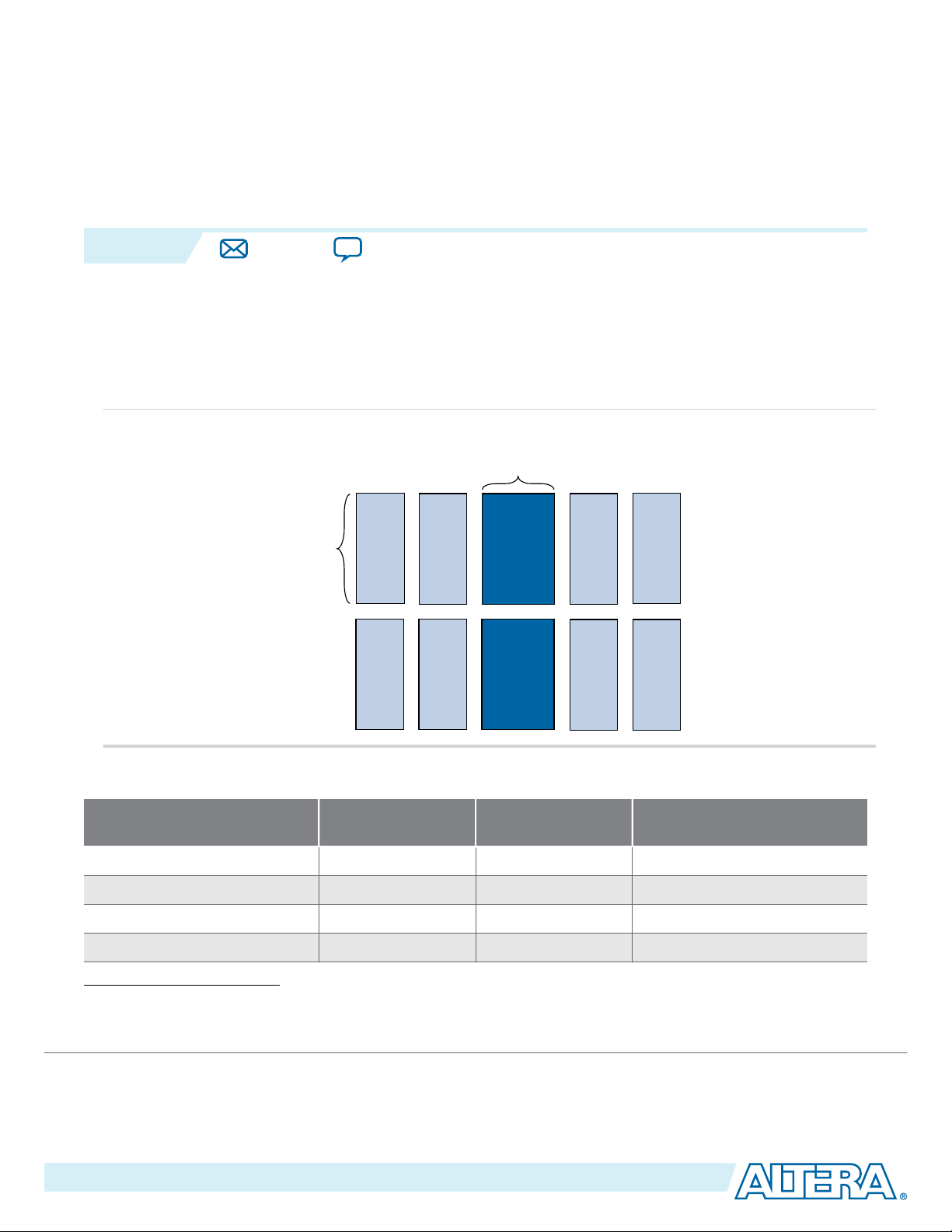
Figure 1-1: Embedded Multipliers Arranged in Columns with Adjacent LABS
Table 1-1: Number of Embedded Multipliers in the MAX 10 Devices
10M02 16 32 16
10M04 20 40 20
10M08 24 48 24
10M16 45 90 45
(1)
These columns show the number of 9 x 9 or 18 x 18 multipliers for each device. The total number of
multipliers for each device is not the sum of all the multipliers.
©
2014 Altera Corporation. All rights reserved. ALTERA, ARRIA, CYCLONE, ENPIRION, MAX, MEGACORE, NIOS, QUARTUS and STRATIX words and logos are
trademarks of Altera Corporation and registered in the U.S. Patent and Trademark Office and in other countries. All other words and logos identified as
trademarks or service marks are the property of their respective holders as described at www.altera.com/common/legal.html. Altera warrants performance
of its semiconductor products to current specifications in accordance with Altera's standard warranty, but reserves the right to make changes to any
products and services at any time without notice. Altera assumes no responsibility or liability arising out of the application or use of any information,
product, or service described herein except as expressly agreed to in writing by Altera. Altera customers are advised to obtain the latest version of device
specifications before relying on any published information and before placing orders for products or services.
Device Embedded
Multipliers
9 x 9 Multipliers
(1)
18 x 18 Multipliers
(1)
ISO
9001:2008
Registered
Page 4

1-2
Embedded Multiplier Block Overview
UG-M10DSP
2014.09.22
Device Embedded
9 x 9 Multipliers
(1)
18 x 18 Multipliers
Multipliers
10M25 55 110 55
10M40 125 250 125
10M50 144 288 144
You can implement soft multipliers by using the M9K memory blocks as look-up tables (LUTs). The
LUTs contain partial results from multiplying input data with coefficients implementing variable depth
and width high-performance soft multipliers for low-cost, high-volume DSP applications. The availability
of soft multipliers increases the number of available multipliers in the device.
Table 1-2: Number of Multipliers in the MAX 10 Devices
Device Embedded
Multipliers
Soft Multipliers
(16 x 16)
(2)
Total Multipliers
10M02 16 12 28
10M04 20 21 41
10M08 24 42 66
10M16 45 61 106
10M25 55 75 130
(1)
(3)
10M40 125 140 265
10M50 144 182 326
(1)
These columns show the number of 9 x 9 or 18 x 18 multipliers for each device. The total number of
multipliers for each device is not the sum of all the multipliers.
(2)
Soft multipliers are implemented in sum of multiplication mode. M9K memory blocks are configured with
18-bit data widths to support 16-bit coefficients. The sum of the coefficients requires 18-bits of resolution to
account for overflow.
(3)
The total number of multipliers may vary, depending on the multiplier mode you use.
Altera Corporation
Embedded Multiplier Block Overview
Send Feedback
Page 5
Embedded Multipliers Features and
CLRN
D Q
ENA
Data A
Data B
aclr
clock
ena
signa
signb
CLRN
D Q
ENA
CLRN
D Q
ENA
Data Out
Embedded Multiplier Block
Output
Register
Input
Register
www.altera.com
101 Innovation Drive, San Jose, CA 95134
2014.09.22
UG-M10DSP
Subscribe
Send Feedback
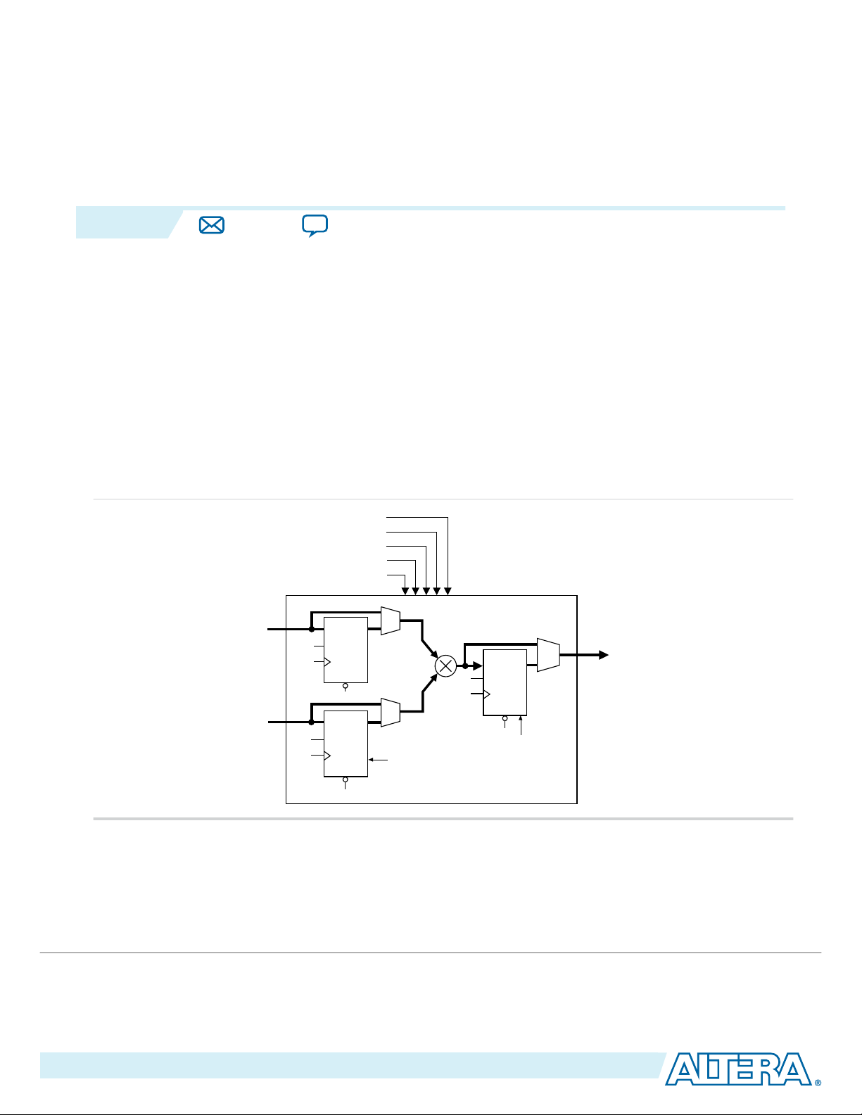
Each embedded multiplier consists of three elements. Depending on the application needs, you can use an
embedded multiplier block in one of two operational modes.
Embedded Multipliers Architecture
Each embedded multiplier consists of the following elements:
• Multiplier stage
• Input and output registers
• Input and output interfaces
Figure 2-1: Multiplier Block Architecture
Architecture
2
Input Register
Depending on the operational mode of the multiplier, you can send each multiplier input signal into
either one of the following:
©
2014 Altera Corporation. All rights reserved. ALTERA, ARRIA, CYCLONE, ENPIRION, MAX, MEGACORE, NIOS, QUARTUS and STRATIX words and logos are
trademarks of Altera Corporation and registered in the U.S. Patent and Trademark Office and in other countries. All other words and logos identified as
trademarks or service marks are the property of their respective holders as described at www.altera.com/common/legal.html. Altera warrants performance
of its semiconductor products to current specifications in accordance with Altera's standard warranty, but reserves the right to make changes to any
products and services at any time without notice. Altera assumes no responsibility or liability arising out of the application or use of any information,
product, or service described herein except as expressly agreed to in writing by Altera. Altera customers are advised to obtain the latest version of device
specifications before relying on any published information and before placing orders for products or services.
ISO
9001:2008
Registered
Page 6

2-2
Multiplier Stage
• An input register
• The multiplier in 9- or 18-bit sections
Each multiplier input signal can be sent through a register independently of other input signals. For
example, you can send the multiplier Data A signal through a register and send the Data B signal directly
to the multiplier.
The following control signals are available to each input register in the embedded multiplier:
• Clock
• Clock enable
• Asynchronous clear
All input and output registers in a single embedded multiplier are fed by the same clock, clock enable, and
asynchronous clear signals.
Multiplier Stage
The multiplier stage of an embedded multiplier block supports 9 × 9 or 18 × 18 multipliers and other
multipliers in between these configurations. Depending on the data width or operational mode of the
multiplier, a single embedded multiplier can perform one or two multiplications in parallel.
Each multiplier operand is a unique signed or unsigned number. Two signals, signa and signb, control
an input of a multiplier and determine if the value is signed or unsigned. If the signa signal is high, the
Data A operand is a signed number. If the signa signal is low, the Data A operand is an unsigned
number.
UG-M10DSP
2014.09.22
The following table lists the sign of the multiplication results for the various operand sign representations.
The results of the multiplication are signed if any one of the operands is a signed value.
signa Value Logic Level signb Value Logic Level
Unsigned Low Unsigned Low Unsigned
Unsigned Low Signed High Signed
Signed High Unsigned Low Signed
Signed High Signed High Signed
You can dynamically change the signa and signb signals to modify the sign representation of the input
operands at run time. You can send the signa and signb signals through a dedicated input register. The
multiplier offers full precision, regardless of the sign representation.
When the signa and signb signals are unused, the Quartus II software sets the multiplier to perform
unsigned multiplication by default.
Output Register
You can register the embedded multiplier output using output registers in either 18- or 36-bit sections.
This depends on the operational mode of the multiplier. The following control signals are available for
each output register in the embedded multiplier:
Data A Data B
Result
Altera Corporation
Embedded Multipliers Features and Architecture
Send Feedback
Page 7
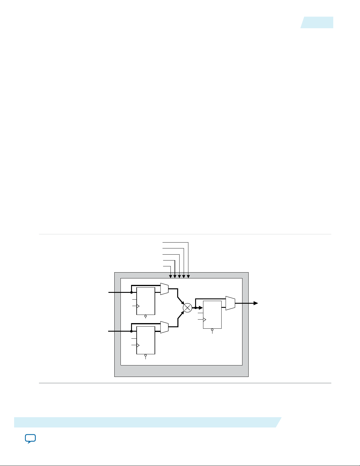
CLRN
D Q
ENA
Data A [17..0]
Data B [17..0]
aclr
clock
ena
signa
signb
CLRN
D Q
ENA
CLRN
D Q
ENA
Data Out [35..0]
18 x 18 Multiplier
Embedded Multiplier
UG-M10DSP
2014.09.22
• Clock
• Clock enable
• Asynchronous clear
All input and output registers in a single embedded multiplier are fed by the same clock, clock enable, and
asynchronous clear signals.
Embedded Multipliers Operational Modes
You can use an embedded multiplier block in one of two operational modes, depending on the applica‐
tion needs:
• One 18-bit x 18-bit multiplier
• Up to two 9-bit x 9-bit independent multipliers
You can also use embedded multipliers of the MAX® 10 devices to implement multiplier adder and
multiplier accumulator functions. The multiplier portion of the function is implemented using embedded
multipliers. The adder or accumulator function is implemented in logic elements (LEs).
18-Bit Multipliers
Embedded Multipliers Operational Modes
2-3
You can configure each embedded multiplier to support a single 18 x 18 multiplier for input widths of 10
to 18 bits.
The following figure shows the embedded multiplier configured to support an 18-bit multiplier.
Figure 2-2: 18-Bit Multiplier Mode
Embedded Multipliers Features and Architecture
Send Feedback
Altera Corporation
Page 8
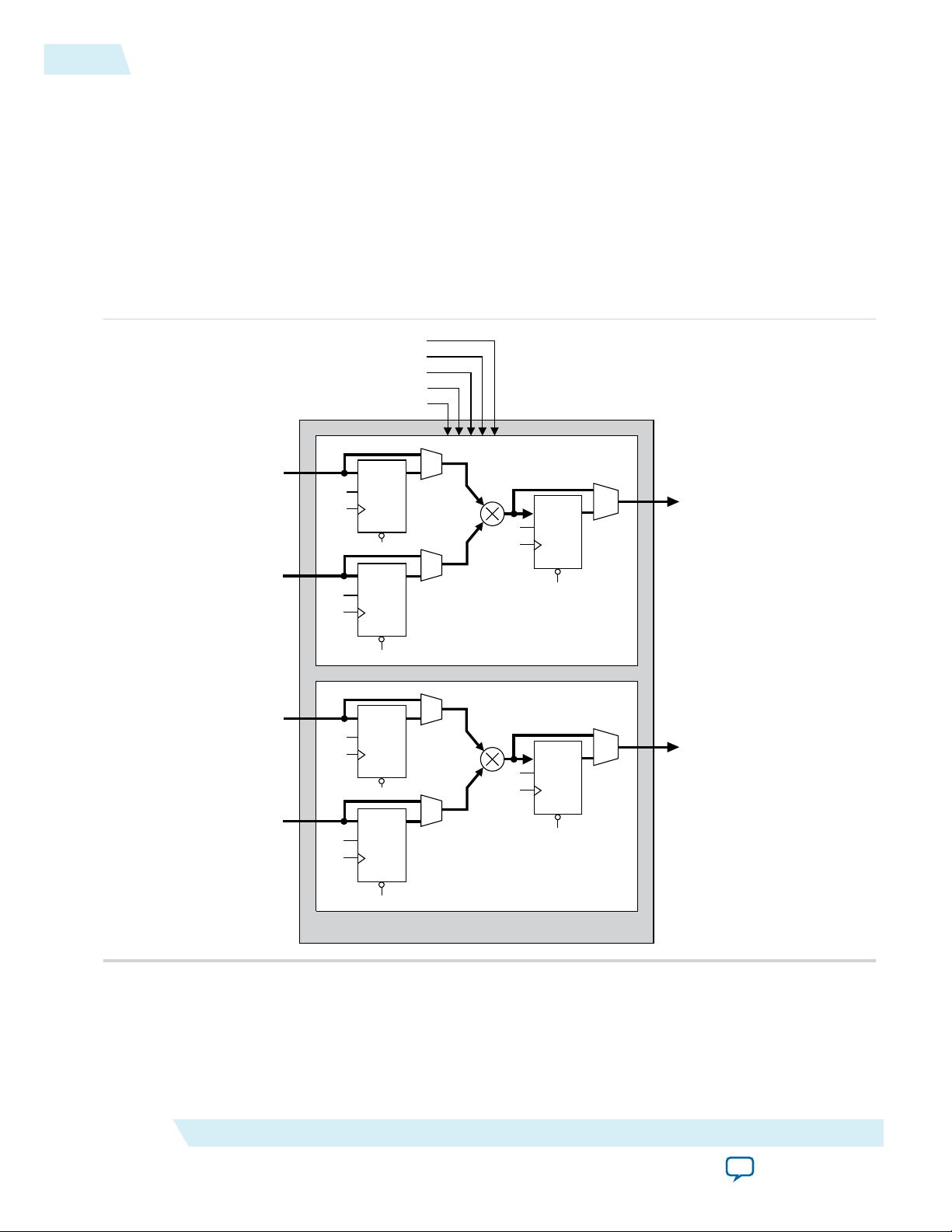
CLRN
D Q
ENA
Data A 0 [8..0]
Data B 0 [8..0]
aclr
clock
ena
signa
signb
CLRN
D Q
ENA
CLRN
D Q
ENA
Data Out 0 [17..0]
9 x 9 Multiplier
Embedded Multiplier
CLRN
D Q
ENA
Data A 1 [8..0]
Data B 1 [8..0]
CLRN
D Q
ENA
CLRN
D Q
ENA
Data Out 1 [17..0]
9 x 9 Multiplier
2-4
9-Bit Multipliers
All 18-bit multiplier inputs and results are independently sent through registers. The multiplier inputs can
accept signed integers, unsigned integers, or a combination of both. Also, you can dynamically change the
signa and signb signals and send these signals through dedicated input registers.
9-Bit Multipliers
You can configure each embedded multiplier to support two 9 × 9 independent multipliers for input
widths of up to 9 bits.
The following figure shows the embedded multiplier configured to support two 9-bit multipliers.
Figure 2-3: 9-Bit Multiplier Mode
UG-M10DSP
2014.09.22
All 9-bit multiplier inputs and results are independently sent through registers. The multiplier inputs can
accept signed integers, unsigned integers, or a combination of both.
Altera Corporation
Embedded Multipliers Features and Architecture
Send Feedback
Page 9

UG-M10DSP
2014.09.22
9-Bit Multipliers
2-5
Each embedded multiplier block has only one signa and one signb signal to control the sign representa‐
tion of the input data to the block. If the embedded multiplier block has two 9 × 9 multipliers the
following applies:
• The Data A input of both multipliers share the same signa signal
• The Data B input of both multipliers share the same signb signal
Embedded Multipliers Features and Architecture
Send Feedback
Altera Corporation
Page 10

2014.09.22
www.altera.com
101 Innovation Drive, San Jose, CA 95134
Embedded Multipliers Implementation Guides
3
UG-M10DSP
Subscribe
Send Feedback
The Quartus II software contains tools for you to create and compile your design, and configure your
device.
You can prepare for device migration, set pin assignments, define placement restrictions, setup timing
constraints, and customize IP cores using the Quartus II software.
Embedded Multipliers Implementation Guides
The Quartus II software contains tools for you to create and compile your design, and configure your
device.
You can prepare for device migration, set pin assignments, define placement restrictions, setup timing
constraints, and customize IP cores using the Quartus II software.
IP Catalog and Parameter Editor
The Quartus II IP Catalog (Tools > IP Catalog) and parameter editor help you easily customize and
integrate IP cores into your project. You can use the IP Catalog and parameter editor to select, customize,
and generate files representing your custom IP variation.
The IP Catalog automatically displays the IP cores available for your target device. Double-click any IP
core name to launch the parameter editor and generate files representing your IP variation. The
parameter editor prompts you to specify your IP variation name, optional ports, architecture features, and
output file generation options. The parameter editor generates a top-level .qsys or .qip file representing the
IP core in your project. Alternatively, you can define an IP variation without an open Quartus II project.
When no project is open, select the Device Family directly in IP Catalog to filter IP cores by device.
The IP Catalog is also available in Qsys (View > IP Catalog). The Qsys IP Catalog includes
Note:
exclusive system interconnect, video and image processing, and other system-level IP that are not
available in the Quartus II IP Catalog.
Use the following features to help you quickly locate and select an IP core:
©
2014 Altera Corporation. All rights reserved. ALTERA, ARRIA, CYCLONE, ENPIRION, MAX, MEGACORE, NIOS, QUARTUS and STRATIX words and logos are
trademarks of Altera Corporation and registered in the U.S. Patent and Trademark Office and in other countries. All other words and logos identified as
trademarks or service marks are the property of their respective holders as described at www.altera.com/common/legal.html. Altera warrants performance
of its semiconductor products to current specifications in accordance with Altera's standard warranty, but reserves the right to make changes to any
products and services at any time without notice. Altera assumes no responsibility or liability arising out of the application or use of any information,
product, or service described herein except as expressly agreed to in writing by Altera. Altera customers are advised to obtain the latest version of device
specifications before relying on any published information and before placing orders for products or services.
ISO
9001:2008
Registered
Page 11
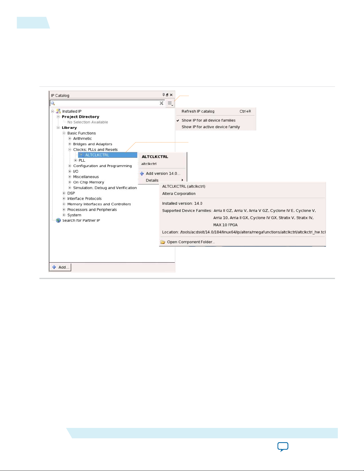
Search and filter IP for your target device
Double-click to customize, right-click for information
3-2
Specifying IP Core Parameters and Options
• Filter IP Catalog to Show IP for active device family or Show IP for all device families.
• Search to locate any full or partial IP core name in IP Catalog. Click Search for Partner IP, to access
partner IP information on the Altera website.
• Right-click an IP core name in IP Catalog to display details about supported devices, installation
location, and links to documentation.
Figure 3-1: Quartus II IP Catalog
UG-M10DSP
2014.09.22
Note: The IP Catalog and parameter editor replace the MegaWizard™ Plug-In Manager in the Quartus II
software. The Quartus II software may generate messages that refer to the MegaWizard Plug-In
Manager. Substitute "IP Catalog and parameter editor" for "MegaWizard Plug-In Manager" in these
messages.
Specifying IP Core Parameters and Options
Follow these steps to specify IP core parameters and options.
1. In the IP Catalog (Tools > IP Catalog), locate and double-click the name of the IP core to customize.
The parameter editor appears.
2. Specify a top-level name for your custom IP variation. This name identifies the IP core variation files
in your project. If prompted, also specify the target Altera device family and output file HDL
preference. Click OK.
3. Specify parameters and options for your IP variation:
Altera Corporation
Embedded Multipliers Implementation Guides
Send Feedback
Page 12

UG-M10DSP
2014.09.22
• Optionally select preset parameter values. Presets specify all initial parameter values for specific
applications (where provided).
• Specify parameters defining the IP core functionality, port configurations, and device-specific
features.
• Specify options for generation of a timing netlist, simulation model, testbench, or example design
(where applicable).
• Specify options for processing the IP core files in other EDA tools.
4. Click Finish or Generate to generate synthesis and other optional files matching your IP variation
specifications. The parameter editor generates the top-level .qip or .qsys IP variation file and HDL files
for synthesis and simulation. Some IP cores also simultaneously generate a testbench or example
design for hardware testing.
The top-level IP variation is added to the current Quartus II project. Click Project > Add/Remove Files
in Project to manually add a .qip or .qsys file to a project. Make appropriate pin assignments to connect
ports.
Files Generated by IP Cores
The following integer arithmetic IP cores use the MAX 10 device embedded multipliers block:
• LPM_MULT
• ALTMULT_ACCUM (MAC)
• ALTMULT_ADD
• ALTMULT_COMPLEX
Files Generated by IP Cores
3-3
Verilog HDL Prototype Location
You can view the Verilog HDL prototype for the IP cores in the following Verilog Design Files (.v):
Table 3-1: Verilog HDL Prototype Location
Integer Arithmetic Megafunctions Directory Verilog Design File (.v)
LPM_MULT <Quartus II installation directory>
lpm.v
\eda\synthesis
• ALTMULT_ACCUM
• ALTMULT_ADD
<Quartus II installation directory>
\eda\synthesis
altera_mf.v
• ALTMULT_COMPLEX
VHDL Component Declaration Location
You can view the VHDL component declaration for the IP cores in the following VHDL Design Files
(.vhd):
Integer Arithmetic Megafunctions Directory VHDL Design File (.vhd)
LPM_MULT <Quartus II installation directory>
\libraries\vhdl\lpm
• ALTMULT_ACCUM
• ALTMULT_ADD
<Quartus II installation directory>
\libraries\vhdl\altera_mf
• ALTMULT_COMPLEX
LPM_PACK.vhd
altera_mf_components.vhd
Embedded Multipliers Implementation Guides
Send Feedback
Altera Corporation
Page 13

2014.09.22
www.altera.com
101 Innovation Drive, San Jose, CA 95134
LPM_MULT (Multiplier) IP Core References
4
UG-M10DSP
Subscribe
Send Feedback
LPM_MULT Parameter Settings
There are three groups of options: General, General2, and Pipeling.
Table 4-1: LPM_MULT Parameters - General
This table lists the IP core parameters applicable to MAX 10 devices.
GUI Parameter Parameter Condition Value Description
Multiplier configuration — —
How wide should the
‘dataa’ input be?
LPM_
WIDTHA
— 1–256 Specifies the width of the
• Multiply
• Multiply
‘dataa’ input
by ‘datab’
input
‘dataa’ input
by itself
(squaring
operation)
Specifies the multiplier
configuration.
dataa[] port.
How wide should the
‘datab’ input be?
How should the width of
the ‘result’ output be
determined?
LPM_
WIDTHB
LPM_
WIDTHP
— 1–256 Specifies the width of the
datab[] port.
—
• Automatically
calculate the
Specifies how the result
width is determined.
width
• Restrict the
width to [] bits
How should the width of
the ‘result’ output be
determined? >
Restrict the width to []
bits
LPM_
WIDTHP
How should the
width of the
‘result’ output
be determined? >
Restrict the width
1–256 You can set the result
width.
to [] bits = On
©
2014 Altera Corporation. All rights reserved. ALTERA, ARRIA, CYCLONE, ENPIRION, MAX, MEGACORE, NIOS, QUARTUS and STRATIX words and logos are
trademarks of Altera Corporation and registered in the U.S. Patent and Trademark Office and in other countries. All other words and logos identified as
trademarks or service marks are the property of their respective holders as described at www.altera.com/common/legal.html. Altera warrants performance
of its semiconductor products to current specifications in accordance with Altera's standard warranty, but reserves the right to make changes to any
products and services at any time without notice. Altera assumes no responsibility or liability arising out of the application or use of any information,
product, or service described herein except as expressly agreed to in writing by Altera. Altera customers are advised to obtain the latest version of device
specifications before relying on any published information and before placing orders for products or services.
ISO
9001:2008
Registered
Page 14

4-2
LPM_MULT Parameter Settings
Table 4-2: LPM_MULT Parameters - General2
This table lists the IP core parameters applicable to MAX 10 devices.
GUI Parameter Parameter Condition Value Description
UG-M10DSP
2014.09.22
Does the ‘datab’ input
bus have a constant
value?
Which type of multipli‐
cation do you want?
Which multiplier
implementation should
be used?
LPM_
REPRESENTATI
ON
DEDICATED_
MULTIPLIER_
CIRCUITRY
— —
—
—
• No
• Yes, the value
• Unsigned
• Signed
• Use default
• Use the
• Use logic
Table 4-3: LPM_MULT Parameters - Pipeling
This table lists the IP core parameters applicable to MAX 10 devices.
GUI Parameter Parameter Condition Value Description
is []
implementa‐
tion
dedicated
multiplier
circuitry (Not
available for all
families)
elements
You can specify the
constant value of the
‘datab’ input bus, if any.
Specifies the type of
multiplication
performed.
Specifies the multiplier
implementation.
Do you want to
pipeline the function?
Create an ‘aclr’
asynchronous clear
port
Create a ‘clken’ clock
enable clock
What type of optimiza‐
tion do you want?
LPM_PIPELINE —
— Do you want to
pipeline the
function? = Yes,
I want output
latency of []
clock cycles
— Do you want to
pipeline the
function? = Yes,
I want output
latency of []
clock cycles
MAXIMIZE_
—
SPEED
• No
• Yes, I want
output
You can add extra
latency to the outputs,
if any.
latency of []
clock cycles
On or off Specifies asynchronous
clear for the complex
multiplier. Clears the
function asynchro‐
nously when aclr port
is asserted high.
On or off Specifies active high
clock enable for the
clock port of the
complex multiplier
• Default
• Speed
• Area
You can specify if the
type of optimization is
determined by Quartus
II, speed, or area.
Altera Corporation
LPM_MULT (Multiplier) IP Core References
Send Feedback
Page 15

UG-M10DSP
2014.09.22
LPM_MULT Ports
Table 4-4: LPM_MULT IP Core Input Ports
Port Name Required Description
dataa[] Yes Data input. The size of the input port depends on the LPM_
datab[] Yes Data input. The size of the input port depends on the LPM_
clock No Clock input for pipelined usage. For LPM_PIPELINE values
clken No Clock enable for pipelined usage. When the clken port is
aclr No Asynchronous clear port used at any time to reset the
LPM_MULT Ports
WIDTHA parameter value.
WIDTHB parameter value.
other than 0 (default), the clock port must be enabled.
asserted high, the adder/subtractor operation takes place.
When the signal is low, no operation occurs. If omitted, the
default value is 1.
pipeline to all 0s, asynchronously to the clock signal. The
pipeline initializes to an undefined (X) logic level. The
outputs are a consistent, but non-zero value.
4-3
Table 4-5: LPM_MULT IP Core Output Ports
Port Name Required Description
result[] Yes Data output. The size of the output port depends on the
LPM_WIDTHP parameter value. If LPM_WIDTHP < max (LPM_
WIDTHA + LPM_WIDTHB, LPM_WIDTHS) or (LPM_WIDTHA + LPM_
WIDTHS), only the LPM_WIDTHP MSBs are present.
LPM_MULT (Multiplier) IP Core References
Send Feedback
Altera Corporation
Page 16

ALTMULT_ACCUM (Multiply-Accumulate) IP
www.altera.com
101 Innovation Drive, San Jose, CA 95134
2014.09.22
UG-M10DSP
Subscribe
Send Feedback
ALTMULT_ACCUM Parameter Settings
There are four groups of options: General, Extra Modes, Multipliers, and Accumulator.
Table 5-1: ALTMULT_ACCUM Parameters - General
This table lists the IP core parameters applicable to MAX 10 devices.
GUI Parameter Parameter Condition Value Description
What is the number of
multipliers?
All multipliers have
similar configurations
How wide should the A
input buses be?
NUMBER_OF_
— 1 By default, only 1
MULTIPLIERS
— — On By default all
WIDTH_A — 1–256 Specifies the width of A
Core References
multiplier is supported.
multipliers have similar
configurations
input buses.
5
How wide should the B
input buses be?
How wide should the
‘result’ output bus be?
Create a 4th asynchro‐
nous clear input option
WIDTH_B — 1–256 Specifies the width of B
input buses.
WIDTH_
RESULT
— 1–256 Specifies the width of
‘result’ output bus.
— — On or Off Turn on this option if
you want to create a 4
asynchronous clear
input option.
Create an associated
clock enable for each
clock
— — On or Off Turn on this option if
you want to create an
associated clock enable
for each clock.
What is the representa‐
tion format for A
inputs?
©
2014 Altera Corporation. All rights reserved. ALTERA, ARRIA, CYCLONE, ENPIRION, MAX, MEGACORE, NIOS, QUARTUS and STRATIX words and logos are
trademarks of Altera Corporation and registered in the U.S. Patent and Trademark Office and in other countries. All other words and logos identified as
trademarks or service marks are the property of their respective holders as described at www.altera.com/common/legal.html. Altera warrants performance
of its semiconductor products to current specifications in accordance with Altera's standard warranty, but reserves the right to make changes to any
products and services at any time without notice. Altera assumes no responsibility or liability arising out of the application or use of any information,
product, or service described herein except as expressly agreed to in writing by Altera. Altera customers are advised to obtain the latest version of device
specifications before relying on any published information and before placing orders for products or services.
REPRESENTATI
ON_A
—
• Signed
• Unsigned
• Variable
Specifies the represen‐
tation format for A
inputs.
th
ISO
9001:2008
Registered
Page 17

5-2
ALTMULT_ACCUM Parameter Settings
GUI Parameter Parameter Condition Value Description
UG-M10DSP
2014.09.22
‘signa’ input controls
the sign (1 signed/0
unsigned)
PORT_SIGNA Input
Representation >
What is the
representation
format for A
inputs? =
Variable
Register ‘signa’ input — Input
Representation >
More Options
Add an extra pipeline
register
— Input
Representation >
More Options
Input Register > What
is the source for clock
input?
Input Register > What
is the source for
asynchronous clear
SIGN_REG_A Input
Representation >
More Options
SIGN_ACLR_A Input
Representation >
More Options
input?
Pipeline Register >
What is the source for
clock input?
SIGN_
PIPELINE_
REG_A
Input
Representation >
More Options
More Options High ‘signa’ input
indicates signed and
low ‘signa’ input
indicates unsigned.
On or Off Turn on this option if
you want to enable the
register of ‘signa’
input
On or Off Turn on this option if
you want to enable the
extra pipeline register
Clock0–Clock3 Specifies the source for
clock input.
• Aclr0–Aclr2
• None
Specifies the source for
asynchronous clear
input.
Clock0–Clock3 Specifies the source for
clock input.
Pipeline Register >
What is the source for
asynchronous clear
SIGN_
PIPELINE_
ACLR_A
Input
Representation >
More Options
input?
What is the representa‐
tion format for B
REPRESENTATI
ONS_B
inputs?
‘signb’ input controls
the sign (1 signed/0
unsigned)
PORT_SIGNB Input
Representation >
What is the
representation
format for B
inputs? =
Variable
Register ‘signb’ input — Input
Representation >
More Options
Add an extra pipeline
register
— Input
Representation >
More Options
—
• Aclr0–Aclr2
• None
• Signed
• Unsigned
• Variable
Specifies the source for
asynchronous clear
input.
Specifies the represen‐
tation format for B
inputs.
More Options High ‘signb’ input
indicates signed and
low ‘signb’ input
indicates unsigned.
On or Off Turn on this option if
you want to enable the
register of ‘signb’
input
On or Off Turn on this option if
you want to enable the
extra pipeline register
Altera Corporation
ALTMULT_ACCUM (Multiply-Accumulate) IP Core References
Send Feedback
Page 18

UG-M10DSP
2014.09.22
ALTMULT_ACCUM Parameter Settings
GUI Parameter Parameter Condition Value Description
5-3
Input Register > What
is the source for clock
input?
Input Register > What
is the source for
asynchronous clear
SIGN_REG_B Input
Representation >
More Options
SIGN_ACLR_B Input
Representation >
More Options
input?
Pipeline Register >
What is the source for
clock input?
Pipeline Register >
What is the source for
asynchronous clear
SIGN_
PIPELINE_
REG_B
SIGN_
PIPELINE_
ACLR_B
Input
Representation >
More Options
Input
Representation >
More Options
input?
Table 5-2: ALTMULT_ACCUM Parameters - Extra Modes
GUI Parameter Parameter Condition Value Description
Create a shiftout
— — On or Off Turn on this option to
output from A input of
the last multiplier
Clock0–Clock3 Specifies the source for
clock input.
• Aclr0–Aclr2
• None
Specifies the source for
asynchronous clear
input.
Clock0–Clock3 Specifies the source for
clock input.
• Aclr0–Aclr2
• None
Specifies the source for
asynchronous clear
input.
create a shiftout output
from A input of the last
multiplier.
Create a shiftout
output from B input of
the last multiplier
Add extra register(s) at
the output
What is the source for
clock input?
What is the source for
asynchronous clear
input?
Add [] extra latency to
the output
— — On or Off Turn on this option to
— — On By default, output
OUTPUT_REG Outputs
Configuration >
More Options
OUTPUT_ACLR Outputs
Configuration >
More Options
— Outputs
Configuration >
More Options
create a shiftout output
from B input of the last
multiplier.
register must be
enabled for
accumulator.
Clock0–Clock3 Specifies the clock
signal for the registers
on the outputs.
• Aclr0–Aclr2
• None
Specifies the asynchro‐
nous clear signal for
the registers on the
outputs.
0, 1, 2, 3, 4, 5, 6,
7, 8, or 12
Specifies the extra
latency to add to the
output.
ALTMULT_ACCUM (Multiply-Accumulate) IP Core References
Send Feedback
Altera Corporation
Page 19

5-4
ALTMULT_ACCUM Parameter Settings
GUI Parameter Parameter Condition Value Description
UG-M10DSP
2014.09.22
Which multiplieradder implementation
should be used?
DEDICATED_
MULTIPLIER_
CIRCUITRY
—
Table 5-3: ALTMULT_ACCUM Parameters - Multipliers
This table lists the IP core parameters applicable to MAX 10 devices.
GUI Parameter Parameter Condition Value Description
Register input A of the
— — On or Off Turn on to enable
multiplier
What is the source for
clock input?
INPUT_REG_A
• Input
Configuration
> Register
input A of the
multiplier =
On
• Input
Configuration
> More
Options
• Use the
default
implementa‐
Specifies the
multiplier-adder
implementation.
tion
• Use dedicated
multiplier
circuitry (Not
available for
all families)
• Use logic
elements
register input A of the
multiplier.
Clock0–Clock3 Specifies the clock port
for the dataa[] port.
What is the source for
asynchronous clear
input?
Register input B of the
multiplier
Altera Corporation
INPUT_ACLR_
A
— — On or Off Turn on to enable
• Input
Configuration
> Register
input A of the
multiplier =
On
• Input
Configuration
> More
Options
• Aclr0–Aclr2
• None
Specifies the asynchro‐
nous clear port for the
dataa[] port.
register input B of the
multiplier.
ALTMULT_ACCUM (Multiply-Accumulate) IP Core References
Send Feedback
Page 20

UG-M10DSP
2014.09.22
ALTMULT_ACCUM Parameter Settings
GUI Parameter Parameter Condition Value Description
5-5
What is the source for
clock input?
What is the source for
asynchronous clear
input?
What is the input A of
the multiplier
connected to?
INPUT_REG_B
INPUT_ACLR_
B
— — Multiplier input By default, input A of
• Input
Configuration
> Register
input B of the
multiplier =
On
• Input
Configuration
> More
Options
• Input
Configuration
> Register
input B of the
multiplier =
On
• Input
Configuration
> More
Options
Clock0–Clock3 Specifies the clock port
for the datab[] port.
• Aclr0–Aclr2
• None
Specifies the asynchro‐
nous clear port for the
datab[] port.
the multiplier is always
connected to the
multiplier’s input.
What is the input B of
the multiplier
connected to?
Register output of the
multiplier
What is the source for
clock input?
— — Multiplier input By default, input B of
— — On or Off Turn on to enable
MULTIPLIER_
REG
• Output
Configuration
> Register
output of the
multiplier =
On
• Output
Configuration
> More
Options
the multiplier is always
connected to the
multiplier’s input.
register output of the
multiplier.
Clock0–Clock3 Specifies the clock
signal for the register
that immediately
follows the multiplier.
ALTMULT_ACCUM (Multiply-Accumulate) IP Core References
Send Feedback
Altera Corporation
Page 21

5-6
ALTMULT_ACCUM Parameter Settings
GUI Parameter Parameter Condition Value Description
UG-M10DSP
2014.09.22
What is the source for
asynchronous clear
input?
MULTIPLIER_
ACLR
• Output
Configuration
> Register
output of the
multiplier =
On
• Output
Configuration
> More
Options
Table 5-4: ALTMULT_ACCUM Parameters - Accumulator
This table lists the IP core parameters applicable to MAX 10 devices.
GUI Parameter Parameter Condition Value Description
Create an ‘accum_
sload’ input port
— — On or off Dynamically specifies
• Aclr0–Aclr2
• None
Specifies the asynchro‐
nous clear signal of the
register that follows the
corresponding
multiplier.
whether the
accumulator value is
constant. If the accum_
sload port is high,
then the multiplier
output is loaded into
the accumulator.
Register ‘accum_sload’
input
Add an extra pipeline
register
—
—
• Accumulator
> Create an
‘accum_sload’
input port =
On
• Accumulator
> More
Options
• Accumulator
> Create an
‘accum_
sload’ input
port = On
• Accumulator
> More
Options
On or off Turn on to enable
register ‘accum_sload’
input.
On or off Turn on this option if
you want to enable the
extra pipeline register
Altera Corporation
ALTMULT_ACCUM (Multiply-Accumulate) IP Core References
Send Feedback
Page 22

UG-M10DSP
2014.09.22
ALTMULT_ACCUM Parameter Settings
GUI Parameter Parameter Condition Value Description
5-7
Input Register > What
is the source for clock
input?
Input Register > What
is the source for
asynchronous clear
input?
Pipeline Register >
What is the source for
clock input?
ACCUM_
SLOAD_REG
ACCUM_
SLOAD_ACLR
ACCUM_
SLOAD_
PIPELINE_REG
• Accumulator
> Create an
‘accum_sload’
input port =
On
• Accumulator
> More
Options
• Accumulator
> Create an
‘accum_
sload’ input
port = On
• Accumulator
> More
Options
• •
Accumulator
> Create an
‘accum_
sload’ input
port = On
• Accumulator
> More
Options
Clock0–Clock3 Specifies the clock
signal for the accum_
sload port.
• Aclr0–Aclr2
• None
Specifies the asynchro‐
nous clear source for
the first register on the
accum_sload input.
Clock0–Clock3 Specifies the source for
clock input.
Pipeline Register >
What is the source for
asynchronous clear
input?
Create an ‘overflow’
output port
Add [] extra latency to
the multiplier output
ACCUM_
SLOAD_
PIPELINE_
ACLR
— — On or Off Overflow port for the
EXTRA_
MULTIPLIER_
LATENCY
• Accumulator
> Create an
‘accum_soad’
input port =
On
• Accumulator
> More
Options
— 0, 1, 2, 3, 4, 5, 6,
• Aclr0–Aclr2
• None
7, 8, or 12
Specifies the source for
asynchronous clear
input.
accumulator
Specifies the number of
clock cycles of latency
for the multiplier
portion of the DSP
block. If the
MULTIPLIER_REG
parameter is specified,
then the specified clock
port is used to add the
latency.
ALTMULT_ACCUM (Multiply-Accumulate) IP Core References
Send Feedback
Altera Corporation
Page 23

5-8
ALTMULT_ACCUM Ports
ALTMULT_ACCUM Ports
Table 5-5: ALTMULT_ACCUM IP Core Input Ports
Port Name Required Description
UG-M10DSP
2014.09.22
accum_sload No
Causes the value on the accumulator feedback path to go to
zero (0) or to accum_sload_upper_data when concatenated
with 0. If the accumulator is adding and the accum_sload port
is high, then the multiplier output is loaded into the
accumulator. If the accumulator is subtracting, then the
opposite (negative value) of the multiplier output is loaded
into the accumulator.
aclr0 No The first asynchronous clear input. The aclr0 port is active
high.
aclr1 No The second asynchronous clear input. The aclr1 port is
active high.
aclr2 No The third asynchronous clear input. The aclr2 port is active
high.
aclr3 No The fourth asynchronous clear input. The aclr3 port is active
high.
addnsub No Controls the functionality of the adder. If the addnsub port is
high, the adder performs an add function; if the addnsub port
is low, the adder performs a subtract function.
clock0 No Specifies the first clock input, usable by any register in the IP
core.
clock1 No Specifies the second clock input, usable by any register in the
IP core.
clock2 No Specifies the third clock input, usable by any register in the IP
core.
clock3 No Specifies the fourth clock input, usable by any register in the
IP core.
dataa[] Yes Data input to the multiplier. The size of the input port
depends on the WIDTH_A parameter value.
datab[] Yes Data input to the multiplier. The size of the input port
depends on the WIDTH_B parameter value.
ena0 No Clock enable for the clock0 port.
ena1 No Clock enable for the clock1 port.
ena2 No Clock enable for the clock2 port.
ena3 No Clock enable for the clock3 port.
Altera Corporation
ALTMULT_ACCUM (Multiply-Accumulate) IP Core References
Send Feedback
Page 24

UG-M10DSP
2014.09.22
Port Name Required Description
signa No Specifies the numerical representation of the dataa[] port. If
signb No Specifies the numerical representation of the datab[] port. If
Table 5-6: ALTMULT_ACCUM IP Core Output Ports
Port Name Required Description
overflow No Overflow port for the accumulator.
result[] Yes Accumulator output port. The size of the output port depends
scanouta[] No Output of the first shift register. The size of the output port
ALTMULT_ACCUM Ports
the signa port is high, the multiplier treats the dataa[] port
as signed two's complement. If the signa port is low, the
multiplier treats the dataa[] port as an unsigned number.
the signb port is high, the multiplier treats the datab[] port
as signed two's complement. If the signb port is low, the
multiplier treats the datab[]port as an unsigned number.
on the WIDTH_RESULT parameter value.
depends on the WIDTH_A parameter value. When instantiating
the ALTMULT_ACCUM IP core with the MegaWizard PlugIn Manager, the MegaWizard Plug-In Manager renames the
scanouta[] port to shiftouta port.
5-9
scanoutb[] No Output of the second shift register. The size of the input port
depends on the WIDTH_B parameter value. When instantiating
the ALTMULT_ACCUM IP core with the MegaWizard PlugIn Manager, the MegaWizard Plug-In Manager renames the
scanoutb[] port to shiftoutb port.
ALTMULT_ACCUM (Multiply-Accumulate) IP Core References
Send Feedback
Altera Corporation
Page 25

ALTMULT_ADD (Multiply-Adder) IP Core
www.altera.com
101 Innovation Drive, San Jose, CA 95134
2014.09.22
UG-M10DSP
Subscribe
Send Feedback
ALTMULT_ADD Parameter Settings
There are three groups of options: General, Extra Modes, and Multipliers.
Table 6-1: ALTMULT_ADD Parameters - General
This table lists the IP core parameters applicable to MAX 10 devices.
GUI Parameter Parameter Condition Value Description
What is the number of
multipliers?
All multipliers have
similar configurations
NUMBER_OF_
MULTIPLIERS
— — On or Off Turn on this option if
— 1, 2, 3, or 4 Specifies the number of
References
multipliers. You can
specify up to four
multipliers.
you want all multipliers
to have similar
configurations.
6
How wide should the A
input buses be?
How wide should the B
input buses be?
How wide should the
‘result’ output bus be?
Create a 4
th
asynchro‐
nous clear input option
WIDTH_A — 1–256 Specifies the width of A
input buses.
WIDTH_B — 1–256 Specifies the width of B
input buses.
WIDTH_
RESULT
— 1–256 Specifies the width of
‘result’ output bus.
— — On or Off Turn on this option if
you want to create a 4
asynchronous clear
input option.
Create an associated
clock enable for each
clock
— — On or Off Turn on this option if
you want to create an
associated clock enable
for each clock.
What is the representa‐
tion format for A
inputs?
©
2014 Altera Corporation. All rights reserved. ALTERA, ARRIA, CYCLONE, ENPIRION, MAX, MEGACORE, NIOS, QUARTUS and STRATIX words and logos are
trademarks of Altera Corporation and registered in the U.S. Patent and Trademark Office and in other countries. All other words and logos identified as
trademarks or service marks are the property of their respective holders as described at www.altera.com/common/legal.html. Altera warrants performance
of its semiconductor products to current specifications in accordance with Altera's standard warranty, but reserves the right to make changes to any
products and services at any time without notice. Altera assumes no responsibility or liability arising out of the application or use of any information,
product, or service described herein except as expressly agreed to in writing by Altera. Altera customers are advised to obtain the latest version of device
specifications before relying on any published information and before placing orders for products or services.
REPRESENTATI
ON_A
—
• Signed
• Unsigned
• Variable
Specifies the represen‐
tation format for A
inputs.
th
ISO
9001:2008
Registered
Page 26

6-2
ALTMULT_ADD Parameter Settings
GUI Parameter Parameter Condition Value Description
UG-M10DSP
2014.09.22
‘signa’ input controls
the sign (1 signed/0
unsigned)
PORT_SIGNA Input
Representation >
What is the
representation
format for A
inputs? =
Variable
Register ‘signa’ input — Input
Representation >
More Options
Add an extra pipeline
register
— Input
Representation >
More Options
Input Register > What
is the source for clock
input?
Input Register > What
is the source for
asynchronous clear
SIGNED_
REGISTER_A
SIGNED_
ACLR_A
Input
Representation >
More Options
Input
Representation >
More Options
input?
Pipeline Register >
What is the source for
clock input?
SIGNED_
PIPELINE_
REGISTER_A
Input
Representation >
More Options
More Options High ‘signa’ input
indicates signed and
low ‘signa’ input
indicates unsigned.
On or Off Turn on this option if
you want to enable the
register of ‘signa’
input
On or Off Turn on this option if
you want to enable the
extra pipeline register
Clock0–Clock3 Specifies the source for
clock input.
• Aclr0–Aclr2
• None
Specifies the source for
asynchronous clear
input.
Clock0–Clock3 Specifies the source for
clock input.
Pipeline Register >
What is the source for
asynchronous clear
SIGNED_
PIPELINE_
ACLR_A
Input
Representation >
More Options
input?
What is the representa‐
tion format for B
REPRESENTATI
ONS_B
inputs?
‘signb’ input controls
the sign (1 signed/0
unsigned)
PORT_SIGNB Input
Representation >
What is the
representation
format for B
inputs? =
Variable
Register ‘signb’ input — Input
Representation >
More Options
Add an extra pipeline
register
— Input
Representation >
More Options
—
• Aclr0–Aclr2
• None
• Signed
• Unsigned
• Variable
Specifies the source for
asynchronous clear
input.
Specifies the represen‐
tation format for B
inputs.
More Options High ‘signb’ input
indicates signed and
low ‘signb’ input
indicates unsigned.
On or Off Turn on this option if
you want to enable the
register of ‘signb’
input
On or Off Turn on this option if
you want to enable the
extra pipeline register
Altera Corporation
ALTMULT_ADD (Multiply-Adder) IP Core References
Send Feedback
Page 27

UG-M10DSP
2014.09.22
ALTMULT_ADD Parameter Settings
GUI Parameter Parameter Condition Value Description
6-3
Input Register > What
is the source for clock
input?
Input Register > What
is the source for
asynchronous clear
SIGNED_
REGISTER_B
SIGNED_
ACLR_B
Input
Representation >
More Options
Input
Representation >
More Options
input?
Pipeline Register >
What is the source for
clock input?
Pipeline Register >
What is the source for
asynchronous clear
SIGNED_
PIPELINE_
REGISTER_B
SIGNED_
PIPELINE_
ACLR_B
Input
Representation >
More Options
Input
Representation >
More Options
input?
Table 6-2: ALTMULT_ADD Parameters - Extra Modes
This table lists the IP core parameters applicable to MAX 10 devices.
GUI Parameter Parameter Condition Value Description
Create a shiftout
— — On or Off Turn on to create a
output from A input of
the last multiplier
Clock0–Clock3 Specifies the source for
clock input.
• Aclr0–Aclr2
• None
Specifies the source for
asynchronous clear
input.
Clock0–Clock3 Specifies the source for
clock input.
• Aclr0–Aclr2
• None
Specifies the source for
asynchronous clear
input.
signal from A input.
Create a shiftout
output from B input of
the last multiplier
Register output of the
adder unit
What is the source for
clock input?
— — On or Off Turn on to create a
— — On or Off Turn on to create a
OUTPUT_
REGISTER
• Outputs
Configuration
> Register
output of the
adder unit =
On
• Outputs
Configuration
> More
Options
signal from B input.
register output of the
adder unit.
Clock0–Clock3 Specifies the clock
signal for the output
register.
ALTMULT_ADD (Multiply-Adder) IP Core References
Send Feedback
Altera Corporation
Page 28

6-4
ALTMULT_ADD Parameter Settings
GUI Parameter Parameter Condition Value Description
UG-M10DSP
2014.09.22
What is the source for
asynchronous clear
input?
What operation should
be performed on
outputs of the first pair
of multipliers?
‘addnsub1’ input
controls the operation
(1 add/0 sub)
OUTPUT_ACLR
MUTIPLIER1_
DIRECTION
— Adder Operation
• Outputs
Configuration
> Register
output of the
adder unit =
On
• Outputs
Configuration
> More
Options
General > What
is the number of
multipliers? = 2,
3, or 4
> What
operation should
be performed on
outputs of the
first pair of
multipliers? =
Variable
• Aclr0–Aclr2
• None
• Add
• Subtract
• Variable
Specifies the source for
asynchronous clear
input.
Specifies whether the
second multiplier adds
or subtracts its value
from the sum. Values
are add and subtract. If
Variable is selected the
addnsub1 port is used.
More Options High ‘addnsub1’ input
indicates add and low
‘addnsub1’ input
indicates subtract.
Register ‘addnsub1'
input
Add an extra pipeline
register
Input Register > What
is the source for clock
input?
Input Register > What
is the source for
asynchronous clear
input?
Pipeline Register >
What is the source for
clock input?
— — On or Off Turn on this option if
— — On or Off Turn on this option if
ADDNSUB_
MULTIPLIER_
REGISTER[1]
ADDSUB_
MULTIPLIER_
ACLR[1]
ADDNSUB_
MULTIPLIER_
PIPELINE_
REGISTER[1]
Adder Operation
> More Options
Adder Operation
> More Options
Adder Operation
> More Options
you want to enable the
register of ‘addnsub1’
input
you want to enable the
extra pipeline register
Clock0–Clock3 Specifies the source for
clock input.
• Aclr0–Aclr2
• None
Specifies the source for
asynchronous clear
input.
Clock0–Clock3 Specifies the source for
clock input.
Altera Corporation
ALTMULT_ADD (Multiply-Adder) IP Core References
Send Feedback
Page 29

UG-M10DSP
2014.09.22
ALTMULT_ADD Parameter Settings
GUI Parameter Parameter Condition Value Description
6-5
Pipeline Register >
What is the source for
asynchronous clear
input?
What operation should
be performed on
outputs of the second
pair of multipliers?
‘addnsub3’ input
controls the sign (1
add/0 sub) - More
Options
Register ‘addnsub3’
input
Add an extra pipeline
register
ADDNSUB_
MULTIPLIER_
PIPELINE_
ACLR[1]
MUTIPLIER3_
DIRECTION
— — — High ‘addnsub3’ input
— — On or Off Turn on this option if
— — On or Off Turn on this option if
Adder Operation
> More Options
General > What
is the number of
multipliers? = 4
• Aclr0–Aclr2
• None
— Specifies whether the
Specifies the source for
asynchronous clear
input.
fourth and all
subsequent oddnumbered multipliers
add or subtract their
results from the total.
Values are add and
subtract. If Variable is
selected, the addnsub3
port is used.
indicates add and low
‘addnsub3’ input
indicates subtract.
you want to enable the
register of ‘addnsub3’
input.
you want to enable the
extra pipeline register.
Input Register > What
is the source for clock
input?
Input Register > What
is the source for
asynchronous clear
input?
Pipeline Register >
What is the source for
clock input?
Pipeline Register >
What is the source for
asynchronous clear
input?
ADDNSUB_
MULTIPLIER_
REGISTER[3]
ADDSUB_
MULTIPLIER_
ACLR[3]
ADDNSUB_
MULTIPLIER_
PIPELINE_
REGISTER[3]
ADDNSUB_
MULTIPLIER_
PIPELINE_
ACLR[3]
Adder Operation
> More Options
Adder Operation
> More Options
Adder Operation
> More Options
Adder Operation
> More Options
Clock0–Clock3 Specifies the source for
clock input.
• Aclr0–Aclr2
• None
Specifies the source for
asynchronous clear
input.
Clock0–Clock3 Specifies the source for
clock input.
• Aclr0–Aclr2
• None
Specifies the source for
asynchronous clear
input.
ALTMULT_ADD (Multiply-Adder) IP Core References
Send Feedback
Altera Corporation
Page 30

6-6
ALTMULT_ADD Parameter Settings
GUI Parameter Parameter Condition Value Description
UG-M10DSP
2014.09.22
Which multiplieradder implementation
should be used?
DEDICATED_
MULTIPLIER_
CIRCUITRY
—
Table 6-3: ALTMULT_ADD Parameters - Multipliers
This table lists the IP core parameters applicable to MAX 10 devices.
GUI Parameter Parameter Condition Value Description
Register input A of the
— — On or Off Turn on to enable
multiplier
What is the source for
clock input?
INPUT_
REGISTER_
A[0..3]
• Input
Configuration
> Register
input A of the
multiplier =
On
• • Input
Configuration
> More
Options
• Use the
default
implementa‐
Specifies the
multiplier-adder
implementation.
tion
• Use dedicated
multiplier
circuitry (Not
available for
all families)
• Use logic
elements
register input A of the
multiplier.
Clock0–Clock3 Specifies the source for
clock input.
What is the source for
asynchronous clear
input?
Register input B of the
multiplier
Altera Corporation
INPUT_ACLR_
A[0..3]
— — On or Off Turn on to enable
• Input
Configuration
> Register
input A of the
multiplier =
On
• Input
Configuration
> More
Options
• Aclr0–Aclr2
• None
Specifies the source for
asynchronous clear
input.
register input B of the
multiplier.
ALTMULT_ADD (Multiply-Adder) IP Core References
Send Feedback
Page 31

UG-M10DSP
2014.09.22
ALTMULT_ADD Parameter Settings
GUI Parameter Parameter Condition Value Description
6-7
What is the source for
clock input?
What is the source for
asynchronous clear
input?
What is the input A of
the multiplier
connected to?
INPUT_
REGISTER_
B[0..3]
INPUT_ACLR_
B[0..3]
INPUT_
SOURCE_
A[0..3]
• Input
Configuration
> Register
input B of the
multiplier =
On
• Input
Configuration
> More
Options
• Input
Configuration
> Register
input B of the
multiplier =
On
• Input
Configuration
> More
Options
—
Clock0–Clock3 Specifies the source for
clock input.
• Aclr0–Aclr2
• None
• Multiplier
input
• Shiftin input
Specifies the source for
asynchronous clear
input.
Specifies the input A of
the multiplier is
connected to either
multiplier input or
shiftin input.
What is the input B of
the multiplier
connected to?
Register output of the
multiplier
What is the source for
clock input?
INPUT_
SOURCE_B[0..3]
— — On or Off Turn on to enable the
MULTIPLIER_
REGISTER[]
—
• Output
Configuration
> Register
output of the
multiplier =
On
• Output
Configuration
> More
Options
• Multiplier
input
• Shiftin input
Specifies the input B of
the multiplier is
connected to either
multiplier input or
shiftin input.
register for output of
the multiplier.
Clock0–Clock3 Specifies the source for
clock input.
ALTMULT_ADD (Multiply-Adder) IP Core References
Send Feedback
Altera Corporation
Page 32

6-8
ALTMULT_ADD Ports
GUI Parameter Parameter Condition Value Description
UG-M10DSP
2014.09.22
What is the source for
asynchronous clear
input?
MULTIPLIER_
ACLR[]
• Output
Configuration
> Register
• Aclr0–Aclr2
• None
Specifies the source for
asynchronous clear
input.
output of the
multiplier =
On
• Output
Configuration
> More
Options
ALTMULT_ADD Ports
Table 6-4: ALTMULT_ADD IP Core Input Ports
Port Name Required Description
dataa[] Yes Data input to the multiplier. Input port [NUMBER_OF_
MULTIPLIERS * WIDTH_A - 1..0] wide.
datab[] Yes Data input to the multiplier. Input port [NUMBER_OF_
MULTIPLIERS * WIDTH_B - 1..0] wide.
clock[] No Clock input port [0..3] to the corresponding register. This port
can be used by any register in the IP core.
aclr[] No Input port [0..3]. Asynchronous clear input to the
corresponding register.
ena[] No Input port [0..3]. Clock enable for the corresponding clock[]
port.
signa No Specifies the numerical representation of the dataa[] port. If the
signa port is high, the multiplier treats the dataa[] port as a
signed two's complement number. If the signa port is low, the
multiplier treats the dataa[] port as an unsigned number.
signb No Specifies the numerical representation of the datab[] port. If the
signb port is high, the multiplier treats the datab[] port as a
signed two's complement number. If the signb port is low, the
multiplier treats the datab[] port as an unsigned number.
Table 6-5: ALTMULT_ADD IP Core Output Ports
Port Name Required Description
result[] Yes Multiplier output port. Output port [WIDTH_RESULT -
1..0] wide.
overflow No Overflow flag. If output_saturation is enabled, overflow
flag is set.
Altera Corporation
ALTMULT_ADD (Multiply-Adder) IP Core References
Send Feedback
Page 33

UG-M10DSP
2014.09.22
ALTMULT_ADD Ports
Port Name Required Description
scanouta[] No Output of scan chain A. Output port [WIDTH_A - 1..0]
wide.
scanoutb[] No Output of scan chain B. Output port [WIDTH_B - 1..0]
wide.
6-9
ALTMULT_ADD (Multiply-Adder) IP Core References
Send Feedback
Altera Corporation
Page 34

ALTMULT_COMPLEX (Complex Multiplier) IP
www.altera.com
101 Innovation Drive, San Jose, CA 95134
2014.09.22
UG-M10DSP
Subscribe
Send Feedback
ALTMULT_COMPLEX Parameter Settings
There are two groups of options: General and Implementation Style/Pipelining.
Table 7-1: ALTMULT_COMPLEX Parameters - General
This table lists the IP core parameters applicable to MAX 10 devices.
GUI Parameter Parameter Condition Value Description
How wide should the A
input buses be?
How wide should the B
input buses be?
How wide should the
‘result’ output bus be?
What is the representa‐
tion format for A
inputs?
WIDTH_A — 1–256 Specifies the width of A
WIDTH_B — 1–256 Specifies the width of B
WIDTH_
— 1–256 Specifies the width of
RESULT
REPRESENTATI
—
ON_A
Core References
• Signed
• Unsigned
7
input buses.
input buses.
‘result’ output bus.
Specifies the represen‐
tation format for A
inputs.
What is the representa‐
tion format for B
inputs?
REPRESENTATI
ONS_B
—
• Signed
• Unsigned
Specifies the represen‐
tation format for B
inputs.
Table 7-2: ALTMULT_COMPLEX Parameters - Implementation Style/Pipelining
This table lists the IP core parameters applicable to MAX 10 devices.
GUI Parameter Parameter Condition Value Description
Which implementa‐
tion style should be
used?
IMPLEMENTATIO
N_STYLE
— Automatically
select a style for
best trade-off for
the current
settings
By default automatic
selection for MAX 10
device is selected.
Quartus II software
will determine the best
implementation based
on the selected device
family and input
width.
©
2014 Altera Corporation. All rights reserved. ALTERA, ARRIA, CYCLONE, ENPIRION, MAX, MEGACORE, NIOS, QUARTUS and STRATIX words and logos are
trademarks of Altera Corporation and registered in the U.S. Patent and Trademark Office and in other countries. All other words and logos identified as
trademarks or service marks are the property of their respective holders as described at www.altera.com/common/legal.html. Altera warrants performance
of its semiconductor products to current specifications in accordance with Altera's standard warranty, but reserves the right to make changes to any
products and services at any time without notice. Altera assumes no responsibility or liability arising out of the application or use of any information,
product, or service described herein except as expressly agreed to in writing by Altera. Altera customers are advised to obtain the latest version of device
specifications before relying on any published information and before placing orders for products or services.
ISO
9001:2008
Registered
Page 35

7-2
ALTMULT_COMPLEX Ports
GUI Parameter Parameter Condition Value Description
UG-M10DSP
2014.09.22
Output latency []
clock cycles
PIPELINE — 0–14 Specifies the number
of clock cycles for
output latency.
Create an asynchro‐
nous Clear input
— — On or off Specifies synchronous
clear for the complex
multiplier. Clears the
function asynchro‐
nously when the aclr
port is asserted high.
Create clock enable
input
— — On or off Specifies active high
clock enable for the
clock port of the
complex multiplier.
ALTMULT_COMPLEX Ports
Table 7-3: ALTMULT_COMPLEX IP Core Input Ports
Port Name Required Description
aclr No Asynchronous clear for the complex multiplier. When the aclr
port is asserted high, the function is asynchronously cleared.
clock Yes Clock input to the ALTMULT_COMPLEX function.
dataa_imag[] Yes Imaginary input value for the data A port of the complex
multiplier. The size of the input port depends on the WIDTH_A
parameter value.
dataa_real[] Yes Real input value for the data A port of the complex multiplier.
The size of the input port depends on the WIDTH_A parameter
value.
datab_imag[] Yes Imaginary input value for the data B port of the complex
multiplier. The size of the input port depends on the WIDTH_B
parameter value.
datab_real[] Yes Real input value for the data B port of the complex multiplier.
The size of the input port depends on the WIDTH_B parameter
value.
ena No Active high clock enable for the clock port of the complex
multiplier.
Table 7-4: ALTMULT_COMPLEX IP Core Output Ports
Port Name Required Description
result_imag Yes Imaginary output value of the multiplier. The size of the output
port depends on the WIDTH_RESULT parameter value.
Altera Corporation
ALTMULT_COMPLEX (Complex Multiplier) IP Core References
Send Feedback
Page 36

UG-M10DSP
2014.09.22
ALTMULT_COMPLEX Ports
Port Name Required Description
result_real Yes Real output value of the multiplier. The size of the output port
depends on the WIDTH_RESULT parameter value.
7-3
ALTMULT_COMPLEX (Complex Multiplier) IP Core References
Send Feedback
Altera Corporation
Page 37

Additional Information for MAX 10 Embedded
www.altera.com
101 Innovation Drive, San Jose, CA 95134
2014.09.22
UG-M10DSP
Subscribe
Multipliers User Guide
Send Feedback
A
Document Revision History for MAX 10 Embedded Multipliers User Guide
Date Version Changes
September
2014
2014.09.22 Initial release.
©
2014 Altera Corporation. All rights reserved. ALTERA, ARRIA, CYCLONE, ENPIRION, MAX, MEGACORE, NIOS, QUARTUS and STRATIX words and logos are
trademarks of Altera Corporation and registered in the U.S. Patent and Trademark Office and in other countries. All other words and logos identified as
trademarks or service marks are the property of their respective holders as described at www.altera.com/common/legal.html. Altera warrants performance
of its semiconductor products to current specifications in accordance with Altera's standard warranty, but reserves the right to make changes to any
products and services at any time without notice. Altera assumes no responsibility or liability arising out of the application or use of any information,
product, or service described herein except as expressly agreed to in writing by Altera. Altera customers are advised to obtain the latest version of device
specifications before relying on any published information and before placing orders for products or services.
ISO
9001:2008
Registered
 Loading...