

Page 1

MAX 10 Embedded Memory User Guide
Subscribe
Send Feedback
UG-
M10MEMORY
2015.05.04
101 Innovation Drive
San Jose, CA 95134
www.altera.com
Page 2

TOC-2
Contents
MAX 10 Embedded Memory Overview.............................................................. 1-1
MAX 10 Embedded Memory Architecture and Features...................................2-1
MAX 10 Embedded Memory General Features...................................................................................... 2-1
Control Signals.................................................................................................................................2-1
Parity Bit............................................................................................................................................2-2
Read Enable.......................................................................................................................................2-2
Read-During-Write......................................................................................................................... 2-3
Byte Enable........................................................................................................................................2-3
Packed Mode Support..................................................................................................................... 2-4
Address Clock Enable Support.......................................................................................................2-5
Asynchronous Clear........................................................................................................................ 2-6
MAX 10 Embedded Memory Operation Modes.....................................................................................2-7
Supported Memory Operation Modes..........................................................................................2-7
MAX 10 Embedded Memory Clock Modes.............................................................................................2-9
Asynchronous Clear in Clock Modes........................................................................................... 2-9
Output Read Data in Simultaneous Read and Write................................................................2-10
Independent Clock Enables in Clock Modes.............................................................................2-10
MAX 10 Embedded Memory Configurations....................................................................................... 2-10
Port Width Configurations.......................................................................................................... 2-10
Mixed-Width Port Configurations..............................................................................................2-11
Maximum Block Depth Configuration.......................................................................................2-12
MAX 10 Embedded Memory Design Consideration..........................................3-1
Implement External Conflict Resolution..................................................................................................3-1
Customize Read-During-Write Behavior.................................................................................................3-1
Same-Port Read-During-Write Mode.......................................................................................... 3-2
Mixed-Port Read-During-Write Mode.........................................................................................3-3
Consider Power-Up State and Memory Initialization............................................................................3-5
Control Clocking to Reduce Power Consumption................................................................................. 3-5
Selecting Read-During-Write Output Choices........................................................................................3-6
RAM: 1-Port IP Core References........................................................................ 4-1
RAM: 1-Port IP Core Signals For MAX 10 Devices................................................................................4-2
RAM: 1-Port IP Core Parameters For MAX 10 Devices........................................................................4-3
RAM: 2-PORT IP Core References.....................................................................5-1
RAM: 2-Ports IP Core Signals (Simple Dual-Port RAM) For MAX 10 Devices................................ 5-5
RAM: 2-Port IP Core Signals (True Dual-Port RAM) for MAX 10 Devices.......................................5-7
Altera Corporation
Page 3

TOC-3
RAM: 2-Port IP Core Parameters for MAX 10 Devices.........................................................................5-9
ROM: 1-PORT IP Core References.....................................................................6-1
ROM: 1-PORT IP Core Signals For MAX 10 Devices............................................................................6-2
ROM: 1-PORT IP Core Parameters for MAX 10 Devices..................................................................... 6-4
ROM: 2-PORT IP Core References.....................................................................7-1
ROM: 2-PORT IP Core Signals for MAX 10 Devices.............................................................................7-3
ROM:2-Port IP Core Parameters For MAX 10 Devices.........................................................................7-5
Shift Register (RAM-based) IP Core References................................................8-1
Shift Register (RAM-based) IP Core Signals for MAX 10 Devices.......................................................8-1
Shift Register (RAM-based) IP Core Parameters for MAX 10 Devices............................................... 8-2
FIFO IP Core References.....................................................................................9-1
FIFO IP Core Signals for MAX 10 Devices..............................................................................................9-2
FIFO IP Core Parameters for MAX 10 Devices.......................................................................................9-4
ALTMEMMULT IP Core References................................................................10-1
ALTMEMMULT IP Core Signals for MAX 10 Devices.......................................................................10-1
ALTMEMMULT IP Core Parameters for MAX 10 Devices............................................................... 10-2
Additional Information for MAX 10 Embedded Memory User Guide............ A-1
Document Revision History for MAX 10 Embedded Memory User Guide.......................................A-1
Altera Corporation
Page 4

2015.05.04
www.altera.com
101 Innovation Drive, San Jose, CA 95134
MAX 10 Embedded Memory Overview
1
UG-M10MEMORY
Subscribe
Send Feedback
MAX® 10 embedded memory block is optimized for applications such as high throughput packet
processing, embedded processor program, and embedded data storage.
©
2015 Altera Corporation. All rights reserved. ALTERA, ARRIA, CYCLONE, ENPIRION, MAX, MEGACORE, NIOS, QUARTUS and STRATIX words and logos are
trademarks of Altera Corporation and registered in the U.S. Patent and Trademark Office and in other countries. All other words and logos identified as
trademarks or service marks are the property of their respective holders as described at www.altera.com/common/legal.html. Altera warrants performance
of its semiconductor products to current specifications in accordance with Altera's standard warranty, but reserves the right to make changes to any
products and services at any time without notice. Altera assumes no responsibility or liability arising out of the application or use of any information,
product, or service described herein except as expressly agreed to in writing by Altera. Altera customers are advised to obtain the latest version of device
specifications before relying on any published information and before placing orders for products or services.
ISO
9001:2008
Registered
Page 5

MAX 10 Embedded Memory Architecture and
www.altera.com
101 Innovation Drive, San Jose, CA 95134
2015.05.04
UG-M10MEMORY
Subscribe
Send Feedback
The MAX 10 embedded memory structure consists of 9,216-bit (including parity bits) blocks. You can use
each M9K block in different widths and configuration to provide various memory functions such as
RAM, ROM, shift registers, and FIFO.
The following list summarizes the MAX 10 embedded memory features:
• Embedded memory general features
• Embedded memory operation modes
• Embedded memory clock modes
Related Information
MAX 10 Device Overview
For information about MAX 10 devices embedded memory capacity and distribution
MAX 10 Embedded Memory General Features
MAX 10 embedded memory supports the following general features:
Features
2
• 8,192 memory bits per block (9,216 bits per block including parity).
• Independent read-enable (rden) and write-enable (wren) signals for each port.
• Packed mode in which the M9K memory block is split into two 4.5 K single-port RAMs.
• Variable port configurations.
• Single-port and simple dual-port modes support for all port widths.
• True dual-port (one read and one write, two reads, or two writes) operation.
• Byte enables for data input masking during writes.
• Two clock-enable control signals for each port (port A and port B).
• Initialization file to preload memory content in RAM and ROM modes.
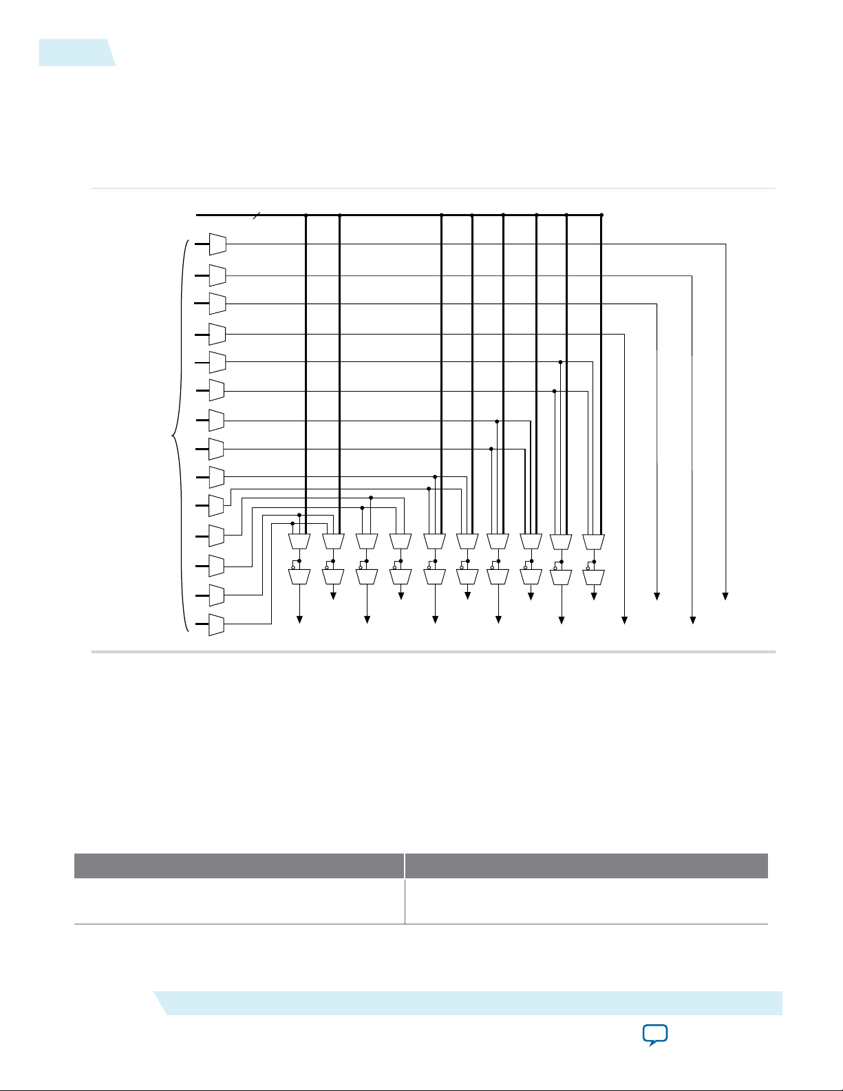
Control Signals
The clock-enable control signal controls the clock entering the input and output registers and the entire
M9K memory block. This signal disables the clock so that the M9K memory block does not see any clock
edges and does not perform any operations.
©
2015 Altera Corporation. All rights reserved. ALTERA, ARRIA, CYCLONE, ENPIRION, MAX, MEGACORE, NIOS, QUARTUS and STRATIX words and logos are
trademarks of Altera Corporation and registered in the U.S. Patent and Trademark Office and in other countries. All other words and logos identified as
trademarks or service marks are the property of their respective holders as described at www.altera.com/common/legal.html. Altera warrants performance
of its semiconductor products to current specifications in accordance with Altera's standard warranty, but reserves the right to make changes to any
products and services at any time without notice. Altera assumes no responsibility or liability arising out of the application or use of any information,
product, or service described herein except as expressly agreed to in writing by Altera. Altera customers are advised to obtain the latest version of device
specifications before relying on any published information and before placing orders for products or services.
ISO
9001:2008
Registered
Page 6
clock_b
clocken_aclock_a
clocken_b
aclr_b
aclr_a
Dedicated
Row LAB
Clocks
rden_b
rden_a
6
Local
Interconnect
byteena_b
byteena_a
addressstall_b
addressstall_a
wren_a
wren_b
2-2
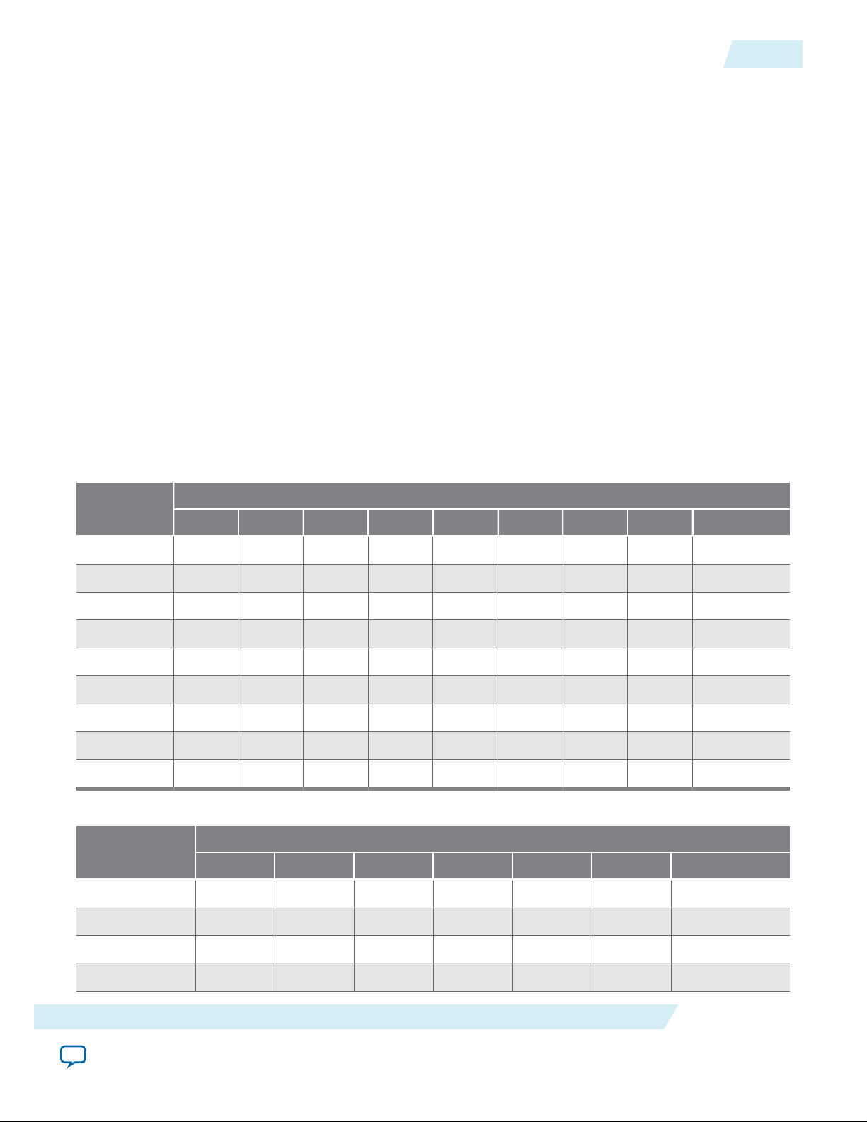
Parity Bit
The rden and wren control signals control the read and write operations for each port of the M9K
memory blocks. You can disable the rden or wren signals independently to save power whenever the
operation is not required.
Figure 2-1: Register Clock, Clear, and Control Signals Implementation in M9K Embedded Memory
Block
UG-M10MEMORY
2015.05.04
Altera Corporation
Parity Bit
You can perform parity checking for error detection with the parity bit along with internal logic
resources. The M9K memory blocks support a parity bit for each storage byte. You can use this bit as
either a parity bit or as an additional data bit. No parity function is actually performed on this bit. If error
detection is not desired, you can use the parity bit as an additional data bit.
Read Enable
M9K memory blocks support the read enable feature for all memory modes.
If you... ...Then
Create the read-enable port and perform a write
operation with the read enable port deasserted
The data output port retains the previous values that
are held during the most recent active read enable.
MAX 10 Embedded Memory Architecture and Features
Send Feedback
Page 7

UG-M10MEMORY
2015.05.04
Read-During-Write
If you... ...Then
2-3
• Activate the read enable during a write
operation, or
• Do not create a read-enable signal
Read-During-Write
The read-during-write operation occurs when a read operation and a write operation target the same
memory location at the same time.
The read-during-write operation operates in the following ways:
• Same-port
• Mixed-port
Related Information
Customize Read-During-Write Behavior on page 3-1
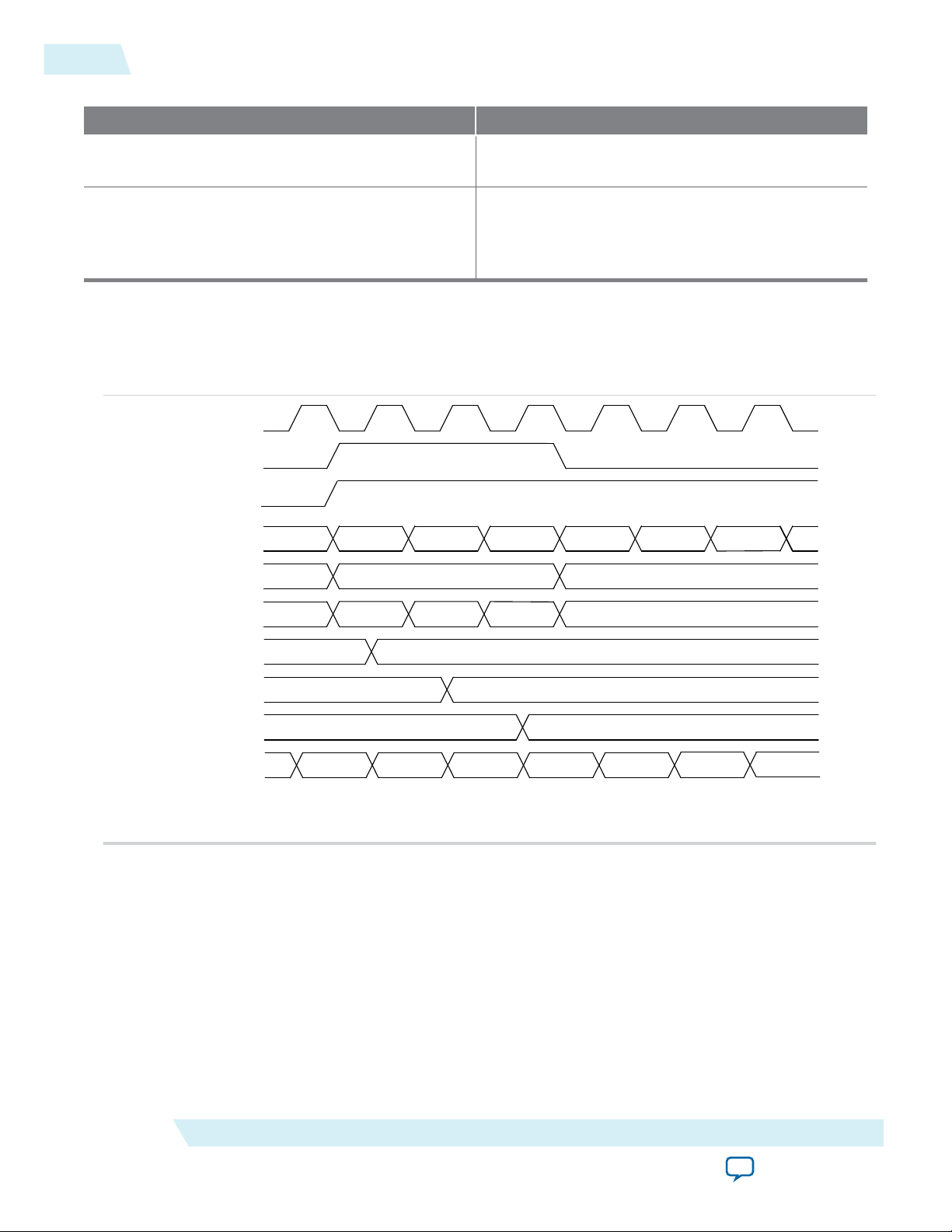
Byte Enable
• Memory block that are implemented as RAMs support byte enables.
• The byte enable controls mask the input data, so that only specific bytes of data are written. The
unwritten bytes retain the values written previously.
• The write enable (wren) signal, together with the byte enable (byteena) signal, control the write
operations on the RAM blocks. By default, the byteena signal is high (enabled) and only the wren
signal controls the writing.
• The byte enable registers do not have a clear port.
• M9K blocks support byte enables when the write port has a data width of ×16, ×18, ×32, or ×36 bits.
• Byte enables operate in a one-hot fashion. The LSB of the byteena signal corresponds to the LSB of the
data bus. For example, if byteena = 01 and you are using a RAM block in ×18 mode, data[8:0] is
enabled and data[17:9] is disabled. Similarly, if byteena = 11, both data[8:0] and data[17:9] are
enabled.
• Byte enables are active high.
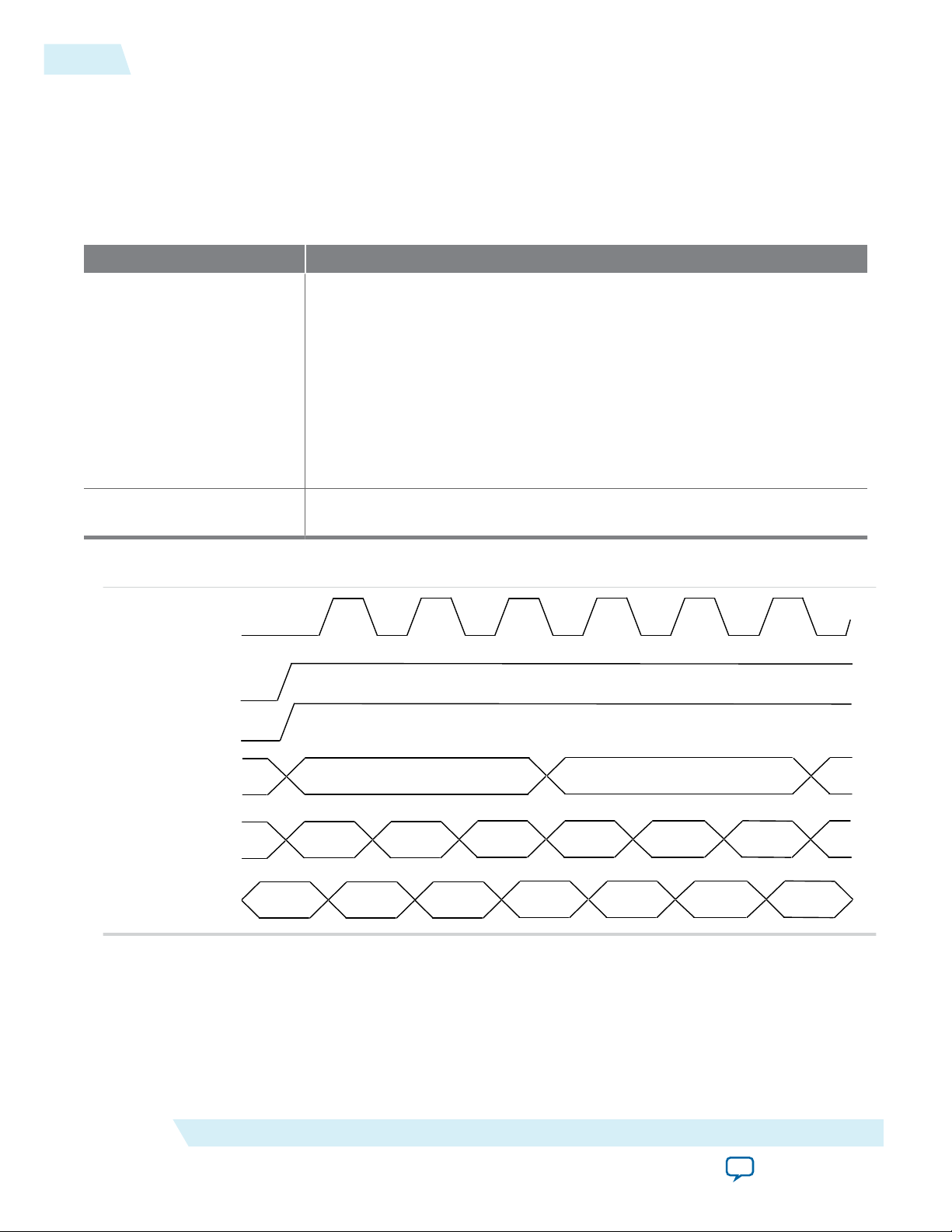
The output port shows:
• the new data being written,
• the old data at that address, or
• a “Don't Care” value when read-during-write
occurs at the same address location.
Byte Enable Controls
Table 2-1: M9K Blocks Byte Enable Selections
byteena[3:0]
datain x 16 datain x 18 datain x 32 datain x 36
[0] = 1 [7:0] [8:0] [7:0] [8:0]
[1] = 1 [15:8] [17:9] [15:8] [17:9]
[2] = 1 — — [23:16] [26:18]
[3] = 1 — — [31:24] [35:27]
MAX 10 Embedded Memory Architecture and Features
Send Feedback
Affected Bytes. Any Combination of Byte Enables is Possible.
Altera Corporation
Page 8
inclock
wren
address
data
q (asynch)
an
XXXX
a0
a1
a2 a0
a1
a2
doutn
ABFF
FFCD
ABCD ABFF FFCD
ABCD
byteena
XX 10 01 11
XXXX
XX
ABCD
ABCD
FFFF
FFFF
FFFF
ABFF
FFCD
contents at a0
contents at a1
contents at a2
rden
For this functional waveform, New Data Mode is selected.
2-4
Data Byte Output
RAM Blocks Operations
Data Byte Output
If you... ...Then
Deassert a byte-enable bit during a write cycle The old data in the memory appears in the
corresponding data-byte output.
Assert a byte-enable bit during a write cycle The corresponding data-byte output depends on the
Quartus® II software setting. The setting can be
either the newly written data or the old data at that
location.
This figure shows how the wren and byteena signals control the RAM operations.
Figure 2-2: Byte Enable Functional Waveform
UG-M10MEMORY
2015.05.04
Altera Corporation
Packed Mode Support
You can implement two single-port memory blocks in a single block under the following conditions:
• Each of the two independent block sizes is less than or equal to half of the M9K block size. The
• Each of the single-port memory blocks is configured in single-clock mode.
Related Information
MAX 10 Embedded Memory Clock Modes on page 2-9
maximum data width for each independent block is 18 bits wide.
MAX 10 Embedded Memory Architecture and Features
Send Feedback
Page 9
address[0]
address[N]
addressstall
clock
address[0]
register
address[N]
register
address[N]
address[0]
inclock
rden
rdaddress
q (synch)
a0
a1 a2 a3 a4 a5
a6
q (asynch)
an
a0
a4
a5
latched address
(inside memory)
dout0
dout1
dout1
dout4
dout1
dout4
dout5
addressstall
a1
doutn-1
dout1
doutn
doutn
dout1
dout0
dout1
UG-M10MEMORY
2015.05.04
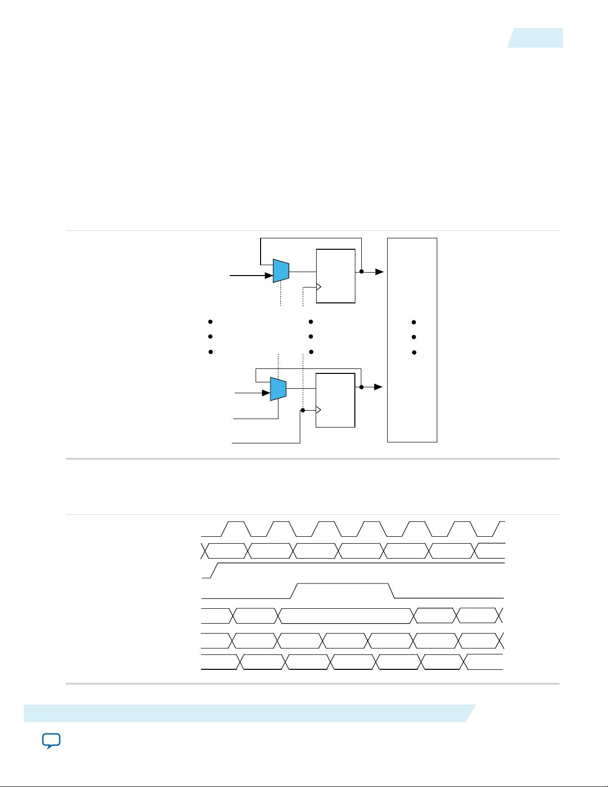
Address Clock Enable Support
• The address clock enable feature holds the previous address value for as long as the address clock
enable signal (addressstall) is enabled (addressstall = 1).
• When you configure M9K memory blocks in dual-port mode, each port has its own independent
address clock enable.
• Use the address clock enable feature to improve the effectiveness of cache memory applications during
a cache-miss.
• The default value for the addressstall signal is low.
• The address register output feeds back to its input using a multiplexer. The addressstall signal
selects the multiplexer output.
Figure 2-3: Address Clock Enable Block Diagram
Address Clock Enable Support
2-5
Address Clock Enable During Read Cycle Waveform
MAX 10 Embedded Memory Architecture and Features
Figure 2-4: Address Clock Enable Waveform During Read Cycle
Send Feedback
Altera Corporation
Page 10
inclock
wren
wraddress
a0 a1 a2 a3 a4 a5
a6
an a0
a4 a5
latched address
(inside memory)
addressstall
a1
data
00
01 02
03 04
05
06
contents at a0
contents at a1
contents at a2
contents at a3
contents at a4
contents at a5
XX
04
XX
00
03
01
XX
02
XX
XX
XX
05
aclr
aclr at latch
clk
q
a1 a0 a1
a2
2-6
Address Clock Enable During Write Cycle Waveform
Address Clock Enable During Write Cycle Waveform
Figure 2-5: Address Clock Enable Waveform During Write Cycle
UG-M10MEMORY
2015.05.04
Asynchronous Clear
You can selectively enable asynchronous clear per logical memory using the RAM: 1-PORT and RAM: 2PORT IP cores.
The M9k block supports asynchronous clear for:
• Read address registers: Asserting asynchronous clear to the read address register during a read
operation might corrupt the memory content.
• Output registers: When applied to output registers, the asynchronous clear signal clears the output
registers and the effects are immediately seen. If your RAM does not use output registers, you can still
clear the RAM outputs using the output latch asynchronous clear feature.
• Output latches
Input registers other than read address registers are not supported.
Note:
Figure 2-6: Output Latch Asynchronous Clear Waveform
Altera Corporation
MAX 10 Embedded Memory Architecture and Features
Send Feedback
Page 11

UG-M10MEMORY
2015.05.04
Related Information
• Internal Memory (RAM and ROM) User Guide.
Resetting Registers in M9K Blocks
There are three ways to reset registers in the M9K blocks:
• Power up the device
• Use the aclr signal for output register only
• Assert the device-wide reset signal using the DEV_CLRn option
MAX 10 Embedded Memory Operation Modes
The M9K memory blocks allow you to implement fully-synchronous SRAM memory in multiple
operation modes. The M9K memory blocks do not support asynchronous (unregistered) memory inputs.
Note: Violating the setup or hold time on the M9K memory block input registers may corrupt memory
contents. This applies to both read and write operations.
Supported Memory Operation Modes
Resetting Registers in M9K Blocks
2-7
Table 2-2: Supported Memory Operation Modes in the M9K Embedded Memory Blocks
Memory Operation Mode Related IP Core Description
Single-port RAM RAM: 1-PORT IP Core
Single-port mode supports non-simultaneous read
and write operations from a single address.
Use the read enable port to control the RAM output
ports behavior during a write operation:
• To show either the new data being written or the
old data at that address, activate the read enable
during a write operation.
• To retain the previous values that are held
during the most recent active read enable,
perform the write operation with the read enable
port deasserted.
Simple dual-port RAM
RAM: 2-PORT IP Core
You can simultaneously perform one read and one
write operations to different locations where the
write operation happens on port A and the read
operation happens on port B.
True dual-port RAM RAM: 2-PORT IP Core
You can perform any combination of two port
operations:
MAX 10 Embedded Memory Architecture and Features
Send Feedback
• two reads, two writes, or,
• one read and one write at two different clock
frequencies.
Altera Corporation
Page 12

2-8
Supported Memory Operation Modes
Memory Operation Mode Related IP Core Description
Single-port ROM ROM: 1-PORT IP Core Only one address port is available for read
operation.
You can use the memory blocks as a ROM.
• Initialize the ROM contents of the memory
blocks using a .mif or .hex file.
• The address lines of the ROM are registered.
• The outputs can be registered or unregistered.
• The ROM read operation is identical to the read
operation in the single-port RAM configuration.
UG-M10MEMORY
2015.05.04
Dual-port ROM ROM: 2-PORT IP Core
Shift-register
Shift Register (RAMbased) IP Core
FIFO FIFO IP Core
The dual-port ROM has almost similar functional
ports as single-port ROM. The difference is dualport ROM has an additional address port for read
operation.
You can use the memory blocks as a ROM.
• Initialize the ROM contents of the memory
blocks using a .mif or .hex file.
• The address lines of the ROM are registered.
• The outputs can be registered or unregistered.
• The ROM read operation is identical to the read
operation in the single-port RAM configuration.
You can use the memory blocks as a shift-register
block to save logic cells and routing resources.
The input data width (w), the length of the taps (m),
and the number of taps (n) determine the size of a
shift register (w × m × n).
You can cascade memory blocks to implement
larger shift registers.
You can use the memory blocks as FIFO buffers.
Memory-based
multiplier
Altera Corporation
• Use the FIFO IP core in single clock FIFO
(SCFIFO) mode and dual clock FIFO (DCFIFO)
mode to implement single- and dual-clock FIFO
buffers in your design.
• Use dual clock FIFO buffers when transferring
data from one clock domain to another clock
domain.
• The M9K memory blocks do not support
simultaneous read and write from an empty
FIFO buffer.
ALTMEMMULT IP Core You can use the memory blocks as a memory-based
multiplier.
MAX 10 Embedded Memory Architecture and Features
Send Feedback
Page 13

UG-M10MEMORY
2015.05.04
Related Information
MAX 10 Embedded Memory Related IPs
MAX 10 Embedded Memory Clock Modes
MAX 10 Embedded Memory Clock Modes
Modes
2-9
Clock Mode Description
Independent
Clock Mode
A separate clock is available for the following
ports:
• Port A—Clock A controls all registers on the
port A side.
• Port B—Clock B controls all registers on the
port B side.
Input/Output
Clock Mode
• M9K memory blocks can implement input
or output clock mode for single-port, true
dual-port, and simple dual-port memory
modes.
• An input clock controls all input registers to
the memory block, including data, address,
byteena, wren, and rden registers.
• An output clock controls the data-output
registers.
Read or Write
Clock Mode
• M9K memory blocks support independent
clock enables for both the read and write
clocks.
• A read clock controls the data outputs, read
address, and read enable registers.
• A write clock controls the data inputs, write
address, and write enable registers.
True
Dual-
Port
Simple
Dual-
Port
Single-
Port
ROM FIFO
Yes — — Yes —
Yes Yes Yes Yes —
— Yes — — Yes
Single-Clock
Mode
Related Information
A single clock, together with a clock enable,
controls all registers of the memory block.
• Packed Mode Support on page 2-4
• Control Clocking to Reduce Power Consumption on page 3-5
• Output Read Data in Simultaneous Read and Write on page 2-10
Asynchronous Clear in Clock Modes
In all clock modes, asynchronous clear is available only for output latches and output registers. For
independent clock mode, this is applicable on port A and port B.
MAX 10 Embedded Memory Architecture and Features
Send Feedback
Yes Yes Yes Yes Yes
Altera Corporation
Page 14

2-10
Output Read Data in Simultaneous Read and Write
Output Read Data in Simultaneous Read and Write
If you perform a simultaneous read/write to the same address location using the read or write clock mode,
the output read data is unknown. If you want the output read data to be a known value, use single-clock
or input/output clock mode and then select the appropriate read-during-write behavior in the RAM: 1PORT and RAM: 2-PORT IP cores.
Related Information
MAX 10 Embedded Memory Clock Modes on page 2-9
Independent Clock Enables in Clock Modes
Table 2-3: Supported Clock Modes for Independent Clock Enables
Clock Mode Description
Read/write Supported for both the read and write clocks.
Independent Supported for the registers of both ports.
MAX 10 Embedded Memory Configurations
UG-M10MEMORY
2015.05.04
Table 2-4: Maximum Configurations Supported for M9K Embedded Memory Blocks
Feature M9K Block
8192 × 1
4096 × 2
2048 × 4
1024 × 8
Configurations (depth × width)
1024 × 9
512 × 16
512 × 18
256 × 32
256 × 36
Port Width Configurations
The following equation defines the port width configuration: Memory depth (number of words) × Width
of the data input bus.
Altera Corporation
MAX 10 Embedded Memory Architecture and Features
Send Feedback
Page 15
UG-M10MEMORY
2015.05.04
• If your port width configuration (either the depth or the width) is more than the amount an internal
memory block can support, additional memory blocks (of the same type) are used. For example, if you
configure your M9K as 512 × 36, which exceeds the supported port width of 512 × 18, two M9Ks are
used to implement your RAM.
• In addition to the supported configuration provided, you can set the memory depth to a non-power of
two, but the actual memory depth allocated can vary. The variation depends on the type of resource
implemented.
• If the memory is implemented in dedicated memory blocks, setting a non-power of two for the
memory depth reflects the actual memory depth.
• When you implement your memory using dedicated memory blocks, refer to the Fitter report to check
the actual memory depth.
Mixed-Width Port Configurations
The mixed-width port configuration support allows you to read and write different data widths to an
M9K memory block. The following memory modes support the mixed-width port configuration:
• Simple dual-port RAM
• True dual-port RAM
• FIFO
Mixed-Width Port Configurations
2-11
M9K Block Mixed-Width Configurations (Simple Dual-Port RAM)
Read Port
8192 × 1 4096 × 2 2048 × 4 1024 × 8 512 × 16 256 × 32 1024 × 9 512 × 18 256 × 36
8192 × 1 Yes Yes Yes Yes Yes Yes — — —
4096 × 2 Yes Yes Yes Yes Yes Yes — — —
2048 × 4 Yes Yes Yes Yes Yes Yes — — —
1024 × 8 Yes Yes Yes Yes Yes Yes — — —
512 × 16 Yes Yes Yes Yes Yes Yes — — —
256 × 32 Yes Yes Yes Yes Yes Yes — — —
1024 × 9 — — — — — — Yes Yes Yes
512 × 18 — — — — — — Yes Yes Yes
256 × 36 — — — — — — Yes Yes Yes
Write Port
M9K Block Mixed-Width Configurations (True Dual-Port RAM Mode)
Read Port
8192 × 1 4096 × 2 2048 × 4 1024 × 8 512 × 16 1024 × 9 512 × 18
Write Port
8192 × 1 Yes Yes Yes Yes Yes — —
4096 × 2 Yes Yes Yes Yes Yes — —
2048 × 4 Yes Yes Yes Yes Yes — —
1024 × 8 Yes Yes Yes Yes Yes — —
MAX 10 Embedded Memory Architecture and Features
Send Feedback
Altera Corporation
Page 16

2-12
Maximum Block Depth Configuration
UG-M10MEMORY
2015.05.04
Read Port
8192 × 1 4096 × 2 2048 × 4 1024 × 8 512 × 16 1024 × 9 512 × 18
Write Port
512 × 16 Yes Yes Yes Yes Yes — —
1024 × 9 — — — — — Yes Yes
512 × 18 — — — — — Yes Yes
Maximum Block Depth Configuration
The Set the maximum block depth parameter allows you to set the maximum block depth of the
dedicated memory block you use. You can slice the memory block to your desired maximum block depth.
For example, the capacity of an M9K block is 9,216 bits, and the default memory depth is 8K, in which
each address is capable of storing 1 bit (8K × 1). If you set the maximum block depth to 512, the M9K
block is sliced to a depth of 512 and each address is capable of storing up to 18 bits (512 × 18).
Use this parameter to save power usage in your devices and to reduce the total number of memory blocks
used. However, this parameter might increase the number of LEs and affects the design performance.
When the RAM is sliced shallower, the dynamic power usage decreases. However, for a RAM block with a
depth of 256, the power used by the extra LEs starts to outweigh the power gain achieved by shallower
slices.
The maximum block depth must be in a power of two, and the valid values vary among different
dedicated memory blocks.
This table lists the valid range of maximum block depth for M9K memory blocks.
Table 2-5: Valid Range of Maximum Block Depth for M9K Memory Blocks
Memory Block Valid Range
M9K 256 - 8K. The maximum block depth must be in a power of two.
The IP parameter editor prompts an error message if you enter an invalid value for the maximum block
depth. Altera recommends that you set the value of the Set the maximum block depth parameter to Auto
if you are unsure of the appropriate maximum block depth to set or the setting is not important for your
design. The Auto setting enables the Compiler to select the maximum block depth with the appropriate
port width configuration for the type of internal memory block of your memory.
Altera Corporation
MAX 10 Embedded Memory Architecture and Features
Send Feedback
Page 17
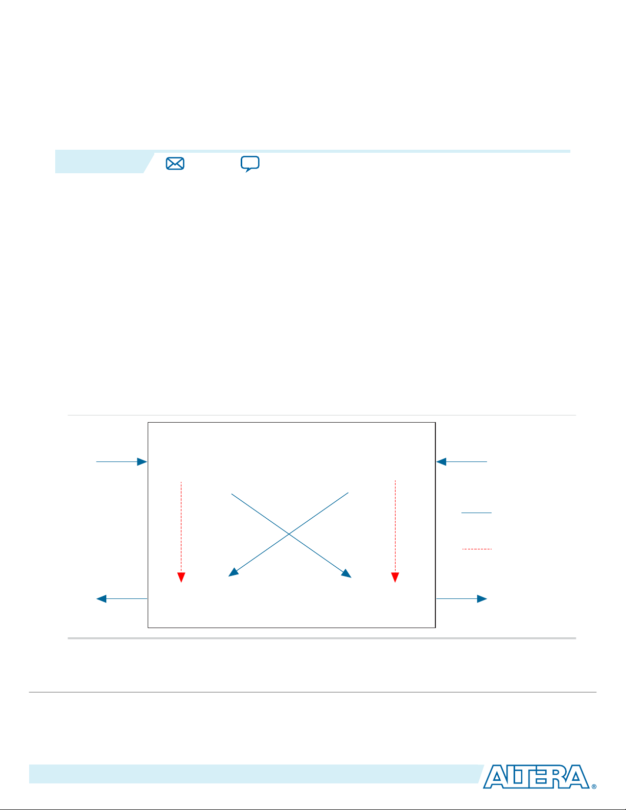
MAX 10 Embedded Memory Design
Port A
data in
Port B
data in
Port A
data out
Port B
data out
Mixed-port
data flow
Same-port
data flow
FPGA Device
www.altera.com
101 Innovation Drive, San Jose, CA 95134
Consideration
2015.05.04
UG-M10MEMORY
There are several considerations that require your attention to ensure the success of your designs.
Subscribe
Implement External Conflict Resolution
In the true dual-port RAM mode, you can perform two write operations to the same memory location.
However, the memory blocks do not have internal conflict resolution circuitry.
To avoid unknown data being written to the address, implement external conflict resolution logic to the
memory block.
Customize Read-During-Write Behavior
Customize the read-during-write behavior of the memory blocks to suit your design requirements.
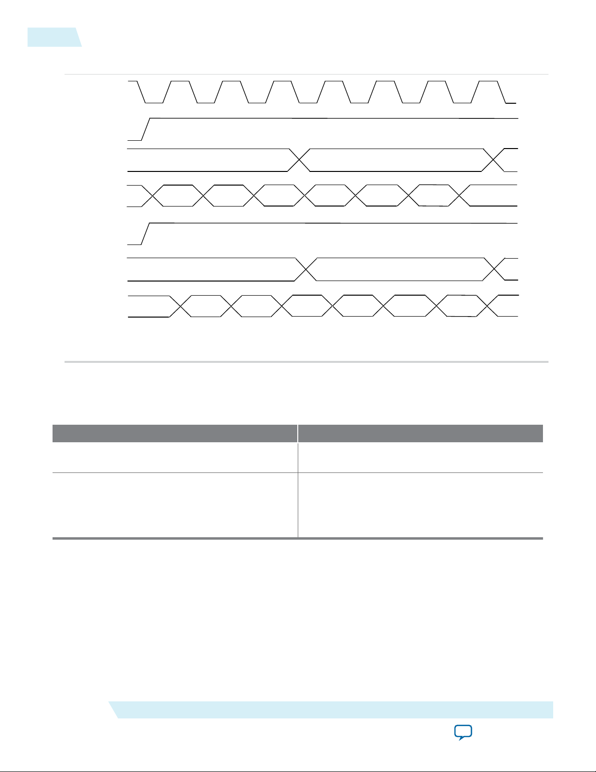
Figure 3-1: Difference Between the Two Types of Read-during-Write Operations —Same Port and
Mixed Port.
Send Feedback
3
Related Information
Read-During-Write on page 2-3
©
2015 Altera Corporation. All rights reserved. ALTERA, ARRIA, CYCLONE, ENPIRION, MAX, MEGACORE, NIOS, QUARTUS and STRATIX words and logos are
trademarks of Altera Corporation and registered in the U.S. Patent and Trademark Office and in other countries. All other words and logos identified as
trademarks or service marks are the property of their respective holders as described at www.altera.com/common/legal.html. Altera warrants performance
of its semiconductor products to current specifications in accordance with Altera's standard warranty, but reserves the right to make changes to any
products and services at any time without notice. Altera assumes no responsibility or liability arising out of the application or use of any information,
product, or service described herein except as expressly agreed to in writing by Altera. Altera customers are advised to obtain the latest version of device
specifications before relying on any published information and before placing orders for products or services.
ISO
9001:2008
Registered
Page 18
clk_a
wren_a
address_a
data_a
rden_a
q_a (asynch)
a0 a1
A B C D E F
A B C D E
F
3-2
Same-Port Read-During-Write Mode
UG-M10MEMORY
Same-Port Read-During-Write Mode
The same-port read-during-write mode applies to a single-port RAM or the same port of a true dual-port
RAM.
Table 3-1: Output Modes for Embedded Memory Blocks in Same-Port Read-During-Write Mode
This table lists the available output modes if you select the embedded memory blocks in the same-port readduring-write mode.
Output Mode Description
2015.05.04
"new data"
(flow-through)
"don't care" The RAM outputs reflect the old data at that address before the write
Figure 3-2: Same-Port Read-During-Write: New Data Mode
The new data is available on the rising edge of the same clock cycle on which
the new data is written.
When using New Data mode together with byte enable, you can control the
output of the RAM.
When byte enable is high, the data written into the memory passes to the
output (flow-through).
When byte enable is low, the masked-off data is not written into the memory
and the old data in the memory appears on the outputs. Therefore, the
output can be a combination of new and old data determined by byteena.
operation proceeds.
Altera Corporation
MAX 10 Embedded Memory Design Consideration
Send Feedback
Page 19
clk_a
wren_a
address_a
data_a
rden_a
a0 a1
A B C D E F
a0(old data) a1(old data)A B D E
UG-M10MEMORY
2015.05.04
Figure 3-3: Same Port Read-During-Write: Old Data Mode
Mixed-Port Read-During-Write Mode
3-3
Mixed-Port Read-During-Write Mode
The mixed-port read-during-write mode applies to simple and true dual-port RAM modes where two
ports perform read and write operations on the same memory address using the same clock—one port
reading from the address, and the other port writing to it.
Table 3-2: Output Modes for RAM in Mixed-Port Read-During-Write Mode
Output Mode Description
"old data"
"don't care"
A read-during-write operation to different ports causes the RAM
output to reflect the “old data” value at the particular address.
The RAM outputs “don’t care” or “unknown” value.
MAX 10 Embedded Memory Design Consideration
Send Feedback
Altera Corporation
Page 20
a b
a (old data)
b (old data)
clk_a&b
wren_a
address_a
q_b (asynch)
rden_b
a b
address_b
data_a
A B C D E F
A
B
D E
In Don't Care mode, the old data is replaced with “Don't Care”.
3-4
Mixed-Port Read-During-Write Operation with Dual Clocks
Figure 3-4: Mixed-Port Read-During-Write: Old Data Mode
UG-M10MEMORY
2015.05.04
Mixed-Port Read-During-Write Operation with Dual Clocks
For mixed-port read-during-write operation with dual clocks, the relationship between the clocks
determines the output behavior of the memory.
If You... ...Then
Use the same clock for the two clocks The output is the old data from the address
location.
Use different clocks The output is unknown during the mixed-port
read-during-write operation. This unknown value
may be the old or new data at the address location,
depending on whether the read happens before or
after the write.
Altera Corporation
MAX 10 Embedded Memory Design Consideration
Send Feedback
Page 21

UG-M10MEMORY
2015.05.04
Consider Power-Up State and Memory Initialization
Consider Power-Up State and Memory Initialization
Consider the power-up state of the different types of memory blocks if you are designing logic that
evaluates the initial power-up values, as listed in the following table:
Table 3-3: Initial Power-Up Values of Embedded Memory Blocks
Memory Type Output Registers Power Up Value
3-5
M9K
Used Zero (cleared)
Bypassed Zero (cleared)
By default, the Quartus II software initializes the RAM cells to zero unless you specify a .mif.
All memory blocks support initialization with a .mif. You can create .mif files in the Quartus II software
and specify their use with the RAM IP when you instantiate a memory in your design. Even if a memory is
preinitialized (for example, using a .mif), it still powers up with its output cleared. Only the subsequent
read after power up outputs the preinitialized values.
Only the following MAX 10 configuration modes support memory initialization:
• Single Compressed Image with Memory Initialization
• Single Uncompressed Image with Memory Initialization
Related Information
Selecting Internal Configuration modes.
Provides more information about selecting MAX 10 internal configuration modes.
Control Clocking to Reduce Power Consumption
Reduce AC power consumption in your design by controlling the clocking of each memory block:
• Use the read-enable signal to ensure that read operations occur only when necessary. If your design
does not require read-during-write, you can reduce your power consumption by deasserting the readenable signal during write operations, or during the period when no memory operations occur.
• Use the Quartus II software to automatically place any unused memory blocks in low-power mode to
reduce static power.
• Create independent clock enable for different input and output registers to control the shut down of a
particular register for power saving purposes. From the parameter editor, click More Options (beside
the clock enable option) to set the available independent clock enable that you prefer.
Related Information
MAX 10 Embedded Memory Clock Modes on page 2-9
MAX 10 Embedded Memory Design Consideration
Send Feedback
Altera Corporation
Page 22

3-6
Selecting Read-During-Write Output Choices
Selecting Read-During-Write Output Choices
• Single-port RAM only supports same-port read-during-write, and the clock mode must be either
single clock mode, or input/output clock mode.
• Simple dual-port RAM only supports mixed-port read-during-write, and the clock mode must be
either single clock mode, or input/output clock mode.
• True dual-port RAM supports same port read-during-write and mixed-port read-during-write.
• For same port read-during-write, the clock mode must be either single clock mode, input/output
clock mode, or independent clock mode.
• For mixed port read-during-write, the clock mode must be either single clock mode, or input/
output clock mode.
Note:
If you are not concerned about the output when read-during-write occurs and would like to
improve performance, select Don't Care. Selecting Don't Care increases the flexibility in the type
of memory block being used, provided you do not assign block type when you instantiate the
memory block.
Table 3-4: Output Choices for the Same-Port and Mixed-Port Read-During-Write
UG-M10MEMORY
2015.05.04
Memory Block
M9K
Single-Port RAM Simple Dual-
Port RAM
Same-Port
Read-During-
Write
Don’t Care
New Data
Mixed-Port
Read-During-
Write
Old Data
Don’t Care
Old Data
Same-Port
Read-During-
Write
New Data
Old Data
True Dual-Port RAM
Mixed-Port Read-During-Write
Old Data
Don’t Care
Altera Corporation
MAX 10 Embedded Memory Design Consideration
Send Feedback
Page 23

2015.05.04
data[]
wren
address[]
rden
addressstall_a
clock
clken
q[]
outaclr
data[]
wren
address[]
rden
addressstall_a
inclock
inclocken
outclock
outclocken
q[]
outaclr
www.altera.com
101 Innovation Drive, San Jose, CA 95134
RAM: 1-Port IP Core References
4
UG-M10MEMORY
Subscribe
Send Feedback
The RAM: 1-Port IP core implements the single-port RAM memory mode.
Figure 4-1: RAM: 1-Port IP Core Signals with the Single Clock Option Enabled
Figure 4-2: RAM: 1-Port IP Core Signals with the Dual Clock Option Enabled
©
2015 Altera Corporation. All rights reserved. ALTERA, ARRIA, CYCLONE, ENPIRION, MAX, MEGACORE, NIOS, QUARTUS and STRATIX words and logos are
trademarks of Altera Corporation and registered in the U.S. Patent and Trademark Office and in other countries. All other words and logos identified as
trademarks or service marks are the property of their respective holders as described at www.altera.com/common/legal.html. Altera warrants performance
of its semiconductor products to current specifications in accordance with Altera's standard warranty, but reserves the right to make changes to any
products and services at any time without notice. Altera assumes no responsibility or liability arising out of the application or use of any information,
product, or service described herein except as expressly agreed to in writing by Altera. Altera customers are advised to obtain the latest version of device
specifications before relying on any published information and before placing orders for products or services.
ISO
9001:2008
Registered
Page 24

4-2
RAM: 1-Port IP Core Signals For MAX 10 Devices
RAM: 1-Port IP Core Signals For MAX 10 Devices
Table 4-1: RAM:1-Port IP Core Input Signals
Signal Required Description
data Yes Data input to the memory. The data port is required
and the width must be equal to the width of the q port.
address Yes Address input to the memory.
wren Yes Write enable input for the wraddress port.
addressstall_a Optional Address clock enable input to hold the previous address
of address_a port for as long as the addressstall_a
port is high.
clock Yes The following list describes which of your memory
clock must be connected to the clock port, and port
synchronization in different clocking modes:
• Single clock—Connect your single source clock to
clock port. All registered ports are synchronized by
the same source clock.
• Read/Write—Connect your write clock to clock
port. All registered ports related to write operation,
such as data_a port, address_a port, wren_a port,
and byteena_a port are synchronized by the write
clock.
• Input/Output—Connect your input clock to clock
port. All registered input ports are synchronized by
the input clock.
• Independent clock—Connect your port A clock to
clock port. All registered input and output ports of
port A are synchronized by the port A clock.
UG-M10MEMORY
2015.05.04
clkena
rden Optional Read enable input for rdaddress port.
aclr Optional Asynchronously clear the registered input and output
Altera Corporation
Optional Clock enable input for clock port.
ports. The asynchronous clear effect on the registered
ports can be controlled through their corresponding
asynchronous clear parameter, such as indata_aclr,
wraddress_aclr, and so on.
RAM: 1-Port IP Core References
Send Feedback
Page 25

UG-M10MEMORY
2015.05.04
inclock Optional The following list describes which of your memory
RAM: 1-Port IP Core Parameters For MAX 10 Devices
Signal Required Description
clock must be connected to the inclock port, and port
synchronization in different clock modes:
• Single clock—Connect your single source clock to
inclock port and outclock port. All registered
ports are synchronized by the same source clock.
• Read/Write—Connect your write clock to inclock
port. All registered ports related to write operation,
such as data port, wraddress port, wren port, and
byteena port are synchronized by the write clock.
• Input/Output—Connect your input clock to
inclock port. All registered input ports are
synchronized by the input clock.
4-3
inclocken
outclock Optional The following list describes which of your memory
Optional Clock enable input for inclock port.
clock must be connected to the outclock port, and port
synchronization in different clock modes:
• Single clock—Connect your single source clock to
inclock port and outclock port. All registered
ports are synchronized by the same source clock.
• Read/Write—Connect your read clock to outclock
port. All registered ports related to read operation,
such as rdaddress port, rdren port, and q port are
synchronized by the read clock.
• Input/Output—Connect your output clock to
outclock port. The registered q port is synchron‐
ized by the output clock.
outclocken
Optional Clock enable input for outclock port.
Table 4-2: RAM:1-Port IP Core Output Ports
Signal Required Description
q Yes Data output from the memory. The q port must be
equal to the width data port.
RAM: 1-Port IP Core Parameters For MAX 10 Devices
Table 4-3: RAM: 1-Port IP Core Parameters for MAX 10 Devices
This table lists the IP core parameters applicable to MAX 10 devices.
Parameter Values Description
Parameter Settings: Widths/Blk Type/Clks
RAM: 1-Port IP Core References
Send Feedback
Altera Corporation
Page 26

4-4
RAM: 1-Port IP Core Parameters For MAX 10 Devices
Parameter Values Description
UG-M10MEMORY
2015.05.04
How wide should the 'q' output bus be? 1, 2, 3, 4, 5, 6, 7, 8, 9,
10, 11, 12, 13, 14, 15,
16, 17, 18, 19, 20, 21,
22, 23, 24, 25, 26, 27,
28, 29, 30, 31, 32, 36,
40, 48, 64, 72, 108,
128, 144, and 256.
How many <X>-bit words of memory? 32, 64, 128, 256, 512,
1024, 2048, 4096,
8192, 16384, 32768,
and 65536.
What should the memory block type be?
Auto On/Off
M9K On/Off
LC On/Off
Use default
On/Off
logic cell style
Options
Use Stratix
On/Off
M512
emulation logic
cell style
Specifies the width of the 'q' output bus
in bits.
Specifies the number of <X>-bit
words.
Specifies the memory block type. The
types of memory block that are
available for selection depends on your
target device.
Specifies the logic cell implementation
options. This option is enabled only
when you choose LCs memory type.
Set the maximum block depth to Auto, 32, 64, 128,
256, 512, 1024, 2048,
4096, and 8192
Specifies the maximum block depth in
words. This option is disabled only
when you choose LCs memory type.
What clocking method would you like to use?
Single clock On/Off A single clock and a clock enable
controls all registers of the memory
block.
Dual clock: use separate ‘input’ and
‘output’ clocks
On/Off An input and an output clock controls
all registers related to the data input
and output to/from the memory block
including data, address, byte enables,
read enables, and write enables.
Parameter Settings: Regs/Clkens/Byte Enable/Aclrs
Which ports should be registered?
'data' and 'wren' input ports — This option is automatically enabled.
Specifies whether to register the read
or write input and output ports.
'address' input port — This option is automatically enabled.
Specifies whether to register the read
or write input and output ports.
'q' output port On/Off Specifies whether to register the read
Altera Corporation
or write input and output ports.
RAM: 1-Port IP Core References
Send Feedback
Page 27

UG-M10MEMORY
2015.05.04
RAM: 1-Port IP Core Parameters For MAX 10 Devices
Parameter Values Description
4-5
Create one clock enable signal for each
clock signal.
On/Off Specifies whether to turn on the option
to create one clock enable signal for
each clock signal.
Use clock
enable for port
On/Off Specify whether to use clock enable for
port A input and output registers.
A input
registers
More Options
Use clock
enable for port
A output
On/Off Specify whether to use clock enable for
port A input and output registers.
registers
Create an
'addressstall_a'
input port
On/Off Specifies whether to create clock
enables for address registers. You can
create these ports to act as an extra
active low clock enable input for the
address registers.
Create an ‘aclr’ asynchronous clear for the
registered ports.
On/Off Specifies whether to create an
asynchronous clear port for the
registered ports.
More Options 'q' port On/Off Specifies whether the q port is cleared
by the aclr port.
Create a 'rden' read enable signal On/Off Specifies whether to create a rden read
enable signal.
Parameter Settings: Read During Write Option
Single Port Read During Write Option
What should the q output be when
reading from a memory location being
written to?
• Don't Care
• New Data
• Old Data
Specifies the output behavior when
read-during-write occurs.
• Don't Care—The RAM outputs
"don't care" or "unknown" values
for read-during-write operation.
• New Data—New data is available
on the rising edge of the same clock
cycle on which it was written.
• Old Data— The RAM outputs
reflect the old data at that address
before the write operation
proceeds.
Get x's for write masked bytes instead of
old data when byte enable is used
On/Off Turn on this option to obtain 'X' on
the masked byte.
Parameter Settings: Mem Init
Do you want to specify the initial content of the memory?
RAM: 1-Port IP Core References
Send Feedback
Altera Corporation
Page 28

4-6
RAM: 1-Port IP Core Parameters For MAX 10 Devices
Parameter Values Description
No, leave it blank On/Off Specifies the initial content of the
memory. Initialize the memory to
zero.
UG-M10MEMORY
2015.05.04
Initialize memory content data to XX..X
on power-up in simulation
Yes, use this file for the memory content
data
Allow In-System Memory Content Editor
to capture and update content independ‐
ently of the system clock
On/Off
On/Off Allows you to specify a memory
initialization file (.mif) or a hexadec‐
imal (Intel-format) file (.hex).
Note: The configuration scheme
of your device is Internal
Configuration. In order to
use memory initialization,
you must select a single
image configuration mode
with memory initialization,
for example the Single
Compressed Image with
Memory Initialization
option. You can set the
configuration mode on the
Configuration page of the
Device and Pin Options
dialog box.
On/Off Specifies whether to allow In-System
Memory Content Editor to capture
and update content independently of
the system clock.
The 'Instance ID' of this RAM is — Specifies the RAM ID.
Altera Corporation
RAM: 1-Port IP Core References
Send Feedback
Page 29

2015.05.04
data[]
wren
rdaddress[]
rden
wr_addressstall
clock
enable
q[]
aclr
wraddress[]
byteena_a[]
rd_addressstall
www.altera.com
101 Innovation Drive, San Jose, CA 95134
RAM: 2-PORT IP Core References
5
UG-M10MEMORY
Subscribe
Send Feedback
The RAM: 2-PORT IP core implements the simple dual-port RAM and true dual-port RAM memory
modes.
Figure 5-1: RAM: 2-Port IP Core Signals With the One Read Port and One Write Port, and Single Clock
Options Enabled
©
2015 Altera Corporation. All rights reserved. ALTERA, ARRIA, CYCLONE, ENPIRION, MAX, MEGACORE, NIOS, QUARTUS and STRATIX words and logos are
trademarks of Altera Corporation and registered in the U.S. Patent and Trademark Office and in other countries. All other words and logos identified as
trademarks or service marks are the property of their respective holders as described at www.altera.com/common/legal.html. Altera warrants performance
of its semiconductor products to current specifications in accordance with Altera's standard warranty, but reserves the right to make changes to any
products and services at any time without notice. Altera assumes no responsibility or liability arising out of the application or use of any information,
product, or service described herein except as expressly agreed to in writing by Altera. Altera customers are advised to obtain the latest version of device
specifications before relying on any published information and before placing orders for products or services.
ISO
9001:2008
Registered
Page 30

data[]
wren
rdaddress[]
wr_addressstall
wrclock
wrclocken
rdclock
rdinclocken
q[]
rd_aclr
wraddress[]
rden
rd_addressstall
rdoutclocken
byteena_a[]
rdclocken
data[]
wren
rdaddress[]
rden
wr_addressstall
inclock
inclocken
outclock
outclocken
q[]
in_aclr
out_aclr
wraddress[]
byteena_a[]
rd_addressstall
5-2
RAM: 2-PORT IP Core References
UG-M10MEMORY
Figure 5-2: RAM: 2-Port IP Core Signals with the One Read Port and One Write Port, and Dual Clock: Use
Separate 'Read' and 'Write' Clocks Options Enabled
2015.05.04
Figure 5-3: RAM: 2-Port IP Core Signals with the One Read Port and One Write Port, and Dual Clock: Use
Separate 'Input' and 'Output' Clocks Options Enabled
Altera Corporation
RAM: 2-PORT IP Core References
Send Feedback
Page 31

data_a[]
wren_a
data_b[]
address_b[]
addressstall_a
clock
enable
q_a[]
aclr
address_a[]
wren_b
addressstall_b
rden_a
rden_b
byteena_a[]
q_b[]
UG-M10MEMORY
2015.05.04
Figure 5-4: RAM: 2-Port IP Core Signals with the Two Read/Write Ports and Single Clock Options
Enabled
RAM: 2-PORT IP Core References
5-3
RAM: 2-PORT IP Core References
Altera Corporation
Send Feedback
Page 32

data_a[]
wren_a
data_b[]
address_b[]
addressstall_a
inclock
inclocken
outclock
outclocken
q_a[]
out_aclr
address_a[]
wren_b
addressstall_b
rden_a
rden_b
byteena_a[]
q_b[]
5-4
RAM: 2-PORT IP Core References
Figure 5-5: RAM: 2-Port IP Core Signals with the Two Read/Write Ports and Dual Clock: Use Separate
'Input' and 'Output' Clocks Options Enabled
UG-M10MEMORY
2015.05.04
Altera Corporation
RAM: 2-PORT IP Core References
Send Feedback
Page 33

data_a[]
wren_a
data_b[]
address_b[]
addressstall_a
clock_a
enable_a
clock_b
enable_b
q_a[]
aclr_a
address_a[]
wren_b
addressstall_b
rden_a
rden_b
byteena_a[]
aclr_b
q_b[]
UG-M10MEMORY
2015.05.04
Figure 5-6: RAM: 2-Port IP Core Signals with the Two Read/Write Ports and Dual Clock: Use Separate for
A and B Ports Options Enabled
RAM: 2-Ports IP Core Signals (Simple Dual-Port RAM) For MAX 10 Devices
5-5
RAM: 2-PORT IP Core References
RAM: 2-Ports IP Core Signals (Simple Dual-Port RAM) For MAX 10 Devices
Table 5-1: RAM: 2-Ports IP Core Input Signals (Simple Dual-Port RAM)
Signal Required Description
data Yes Data input to the memory. The data port is required and the
wraddress Yes Write address input to the memory. The wraddress port is
wren Yes Write enable input for wraddress port. The wren port is
rdaddress Yes Read address input to the memory. The rdaddress port is
Send Feedback
width must be equal to the width of the q port.
required and must be equal to the width of the raddress port.
required.
required and must be equal to the width of wraddress port.
Altera Corporation
Page 34

5-6
RAM: 2-Ports IP Core Signals (Simple Dual-Port RAM) For MAX 10 Devices
Signal Required Description
clock Yes The following list describes which of your memory clock must
be connected to the clock port, and port synchronization in
different clock modes:
• Single clock—Connect your single source clock to clock
port. All registered ports are synchronized by the same
source clock.
• Read/Write—Connect your write clock to clock port. All
registered ports related to write operation, such as data_a
port, address_a port, wren_a port, and byteena_a port are
synchronized by the write clock.
• Input/Output—Connect your input clock to clock port. All
registered input ports are synchronized by the input clock.
• Independent clock—Connect your port A clock to clock
port. All registered input and output ports of port A are
synchronized by the port A clock.
UG-M10MEMORY
2015.05.04
inclock
outclock
Yes The following list describes which of your memory clock must
be connected to the inclock port, and port synchronization in
different clock modes:
• Single clock—Connect your single source clock to inclock
port and outclock port. All registered ports are synchron‐
ized by the same source clock.
• Read/Write—Connect your write clock to inclock port. All
registered ports related to write operation, such as data
port, wraddress port, wren port, and byteena port are
synchronized by the write clock.
• Input/Output—Connect your input clock to inclock port.
All registered input ports are synchronized by the input
clock.
Yes The following list describes which of your memory clock must
be connected to the outclock port, and port synchronization in
different clock modes:
• Single clock—Connect your single source clock to inclock
port and outclock port. All registered ports are synchron‐
ized by the same source clock.
• Read/Write—Connect your read clock to outclock port. All
registered ports related to read operation, such as
rdaddress port, rdren port, and q port are synchronized by
the read clock.
• Input/Output—Connect your output clock to outclock
port. The registered q port is synchronized by the output
clock.
rden
Altera Corporation
Optional Read enable input for rdaddress port. The rden port is
supported when the use_eab parameter is set to OFF.
Instantiate the IP core if you want to use read enable feature
with other memory blocks.
RAM: 2-PORT IP Core References
Send Feedback
Page 35

UG-M10MEMORY
2015.05.04
Signal Required Description
byteena_a Optional Byte enable input to mask the data_a port so that only specific
RAM: 2-Port IP Core Signals (True Dual-Port RAM) for MAX 10 Devices
bytes, nibbles, or bits of the data are written. The byteena_a
port is not supported in the following conditions:
• If the implement_in_les parameter is set to ON.
• If the operation_mode parameter is set to ROM.
outclocken Optional Clock enable input for outclock port.
inclocken Optional Clock enable input for inclock port.
Table 5-2: RAM: 2-Ports IP Core Output Signals (Simple Dual-Port RAM)
Signal Required Description
q Yes Data output from the memory. The q port is required, and
must be equal to the width data port.
RAM: 2-Port IP Core Signals (True Dual-Port RAM) for MAX 10 Devices
5-7
Table 5-3: RAM: 2-Port IP Core Input Signals (True Dual-Port RAM)
Signal Required Description
data_a Optional Data input to port A of the memory. The data_a port is
required if the operation_mode parameter is set to any of the
following values:
• SINGLE_PORT
• DUAL_PORT
• BIDIR_DUAL_PORT
address_a Yes Address input to port A of the memory. The address_a port is
required for all operation modes.
wren_a Optional Write enable input for address_a port. The wren_a port is
required if you set the operation_mode parameter to any of the
following values:
• SINGLE_PORT
• DUAL_PORT
• BIDIR_DUAL_PORT
data_b Optional Data input to port B of the memory. The data_b port is
required if the operation_mode parameter is set to BIDIR_
DUAL_PORT.
address_b Optional Address input to port B of the memory. The address_b port is
RAM: 2-PORT IP Core References
Send Feedback
required if the operation_mode parameter is set to the
following values:
• DUAL_PORT
• BIDIR_DUAL_PORT
Altera Corporation
Page 36

5-8
RAM: 2-Port IP Core Signals (True Dual-Port RAM) for MAX 10 Devices
Signal Required Description
wren_b Yes Write enable input for address_b port. The wren_b port is
required if you set the operation_mode parameter to BIDIR_
DUAL_PORT.
clock Yes The following list describes which of your memory clock must
be connected to the clock port, and port synchronization in
different clock modes:
• Single clock—Connect your single source clock to clock
port. All registered ports are synchronized by the same
source clock.
• Read/Write—Connect your write clock to clock port. All
registered ports related to write operation, such as data_a
port, address_a port, wren_a port, and byteena_a port are
synchronized by the write clock.
• Input/Output—Connect your input clock to clock port. All
registered input ports are synchronized by the input clock.
• Independent clock—Connect your port A clock to clock
port. All registered input and output ports of port A are
synchronized by the port A clock.
UG-M10MEMORY
2015.05.04
inclock
outclock
Yes The following list describes which of your memory clock must
be connected to the inclock port, and port synchronization in
different clock modes:
• Single clock—Connect your single source clock to inclock
port and outclock port. All registered ports are synchron‐
ized by the same source clock.
• Read/Write—Connect your write clock to inclock port. All
registered ports related to write operation, such as data
port, wraddress port, wren port, and byteena port are
synchronized by the write clock.
• Input/Output—Connect your input clock to inclock port.
All registered input ports are synchronized by the input
clock.
Yes The following list describes which of your memory clock must
be connected to the outclock port, and port synchronization in
different clock modes:
• Single clock—Connect your single source clock to inclock
port and outclock port. All registered ports are synchron‐
ized by the same source clock.
• Read/Write—Connect your read clock to outclock port. All
registered ports related to read operation, such as
rdaddress port, rdren port, and q port are synchronized by
the read clock.
• Input/Output—Connect your output clock to outclock
port. The registered q port is synchronized by the output
clock.
Altera Corporation
RAM: 2-PORT IP Core References
Send Feedback
Page 37

UG-M10MEMORY
2015.05.04
Signal Required Description
rden_a Optional Read enable input for address_a port. The rden_a port is
RAM: 2-Port IP Core Parameters for MAX 10 Devices
supported depending on your selected memory mode and
memory block.
rden_b Optional Read enable input for address_b port. The rden_b port is
supported depending on your selected memory mode and
memory block.
byteena_a Byte enable input to mask the data_a port so that only specific
bytes, nibbles, or bits of the data are written. The byteena_a
port is not supported in the following conditions:
• If the implement_in_les parameter is set to ON.
• If the operation_mode parameter is set to ROM.
addressstall_a Optional Address clock enable input to hold the previous address of
address_a port for as long as the addressstall_a port is high.
addressstall_b Optional Address clock enable input to hold the previous address of
address_b port for as long as the addressstall_b port is high.
Table 5-4: RAM:2-Port IP Core Output Signals (True Dual-Port RAM)
5-9
Signal Required Description
q_a Yes Data output from Port A of the memory. The q_a port is
required if the operation_mode parameter is set to any of the
following values:
• SINGLE_PORT
• BIDIR_DUAL_PORT
• ROM
The width of q_a port must be equal to the width of data_a
port.
q_b Yes Data output from Port B of the memory. The q_b port is
required if you set the operation_mode to the following values:
• DUAL_PORT
• BIDIR_DUAL_PORT
The width of q_b port must be equal to the width of data_b
port.
RAM: 2-Port IP Core Parameters for MAX 10 Devices
Table 5-5: RAM: 2-Port IP Core Parameters for MAX 10 Devices
This table lists the IP core parameters applicable to MAX 10 devices.
Option Legal Values Description
Parameter Settings: General
RAM: 2-PORT IP Core References
Send Feedback
Altera Corporation
Page 38

5-10
RAM: 2-Port IP Core Parameters for MAX 10 Devices
Option Legal Values Description
UG-M10MEMORY
2015.05.04
How will you be using the dual port RAM?
• With one read port and
one write port
Specifies how you use the
dual port RAM.
• With two read/write ports
How do you want to specify the memory
size?
• As a number of words
• As a number of bits
Determines whether to
specify the memory size in
words or bits.
Parameter Settings: Widths/ Blk Type
How many <X>-bit words of memory? — Specifies the number of <X>
-bit words.
Use different data widths on different ports On/Off Specifies whether to use
different data widths on
different ports.
When you select With
one read port and one
write port, the
following options are
available:
• How wide should
the ‘data_a’ input
bus be?
Specifies the width of the
input and output ports.
• How wide should
The How wide should the
‘q’ output bus be? and the
How wide should the ‘q_b’
output bus be? options are
only available when you turn
on the Use different data
widths on different ports
parameter.
Read/Write Ports
the ‘q’ output bus
be?
When you select
With two read/
write ports, the
following options
are available:
1, 2, 3, 4, 5, 6, 7, 8, 9, 16, 18,
32, 36, 64, 72, 108, 128, 144,
256, and 288
Altera Corporation
• How wide
should the ‘q_a’
output bus be?
• How wide
should the ‘q_b’
output bus be?
RAM: 2-PORT IP Core References
Send Feedback
Page 39

UG-M10MEMORY
2015.05.04
RAM: 2-Port IP Core Parameters for MAX 10 Devices
Option Legal Values Description
5-11
What should the memory block type be?
Option
How should the
memory be
implemented?
Set the maximum block depth to
• Auto
• M9K
• LCs
• Use default logic cell style
• Use Stratix M512
emulation logic cell style
• Auto
• 128
• 256
• 512
• 1024
• 2048
• 4096
• 8192
Specifies the memory block
type. The types of memory
block that are available for
selection depends on your
target device.
The LCs value is only
available under the following
conditions:
• Turn on the With one
read port and one write
port option
• Turn off Use different
data widths on different
ports option.
Specifies the logic cell
implementation options.
This option is enabled only
when you choose LCs
memory type.
Specifies the maximum
block depth in words.
Parameter Settings: Clks/Rd, Byte En
RAM: 2-PORT IP Core References
Send Feedback
Altera Corporation
Page 40

5-12
RAM: 2-Port IP Core Parameters for MAX 10 Devices
Option Legal Values Description
UG-M10MEMORY
2015.05.04
What clocking method would you like to
use?
When you select With one
read port and one write port,
the following values are
available:
• Single clock
• Dual clock: use separate
‘input’ and ‘output’ clocks
• Dual clock: use separate
‘read’ and ‘write’ clocks
When you select With two
read/write ports, the
following options are
available:
• Single clock
• Dual clock: use separate
‘input’ and ‘output’ clocks
• Dual clock: use separate
clocks for A and B ports
Specifies the clocking
method to use.
• Single clock—A single
clock and a clock enable
controls all registers of
the memory block.
• Dual Clock: use separate
‘input’ and ‘output’
clocks—An input and an
output clock controls all
registers related to the
data input and output to/
from the memory block
including data, address,
byte enables, read
enables, and write
enables.
• Dual clock: use separate
‘read’ and ‘write’ clocks—
A write clock controls the
data-input, write-address,
and write-enable registers
while the read clock
controls the data-output,
read-address, and readenable registers.
• Dual clock: use separate
clocks for A and B ports
—Clock A controls all
registers on the port A
side; clock B controls all
registers on the port B
side. Each port also
supports independent
clock enables for both
port A and port B
registers, respectively.
Create a ‘rden’ read enable signal
Create a ‘rden_a’ and ‘rden_b’ read enable
signal
Altera Corporation
On/Off Available when you select
With one read port and one
write port option.
On/Off
• Available when you select
With two read/write
ports option.
• Specifies whether to
create a read enable
signal for Port A and B.
RAM: 2-PORT IP Core References
Send Feedback
Page 41

UG-M10MEMORY
2015.05.04
RAM: 2-Port IP Core Parameters for MAX 10 Devices
Option Legal Values Description
5-13
Byte Enable Ports Create byte enable for
port A
Parameter Settings: Regs/Clkens/Aclrs
Which ports
should be
registered?
When you select With
one read port and one
write port, the
following options are
available:
• Write input ports
‘data_a’,
‘wraddress_a’, and
‘wren_a’
• Read input ports
'rdaddress' and
'rden'
• Read output port(s)
‘q_a’ and 'q_b'
On/Off Specifies whether to create a
byte enable for Port A and B.
Turn on these options if you
want to mask the input data
so that only specific bytes,
nibbles, or bits of data are
written.
On/Off
Specifies whether to register
the read or write input and
output ports.
When you select With
two read/write ports,
the following options
are available:
• Write input ports
‘data_a’,
‘wraddress_a’, and
‘wren_a’ write
input ports
• Read output port(s)
‘q’_a and ‘q_b’
More Option When you select With
one read port and one
write port, the
following options are
available:
• ‘q_b’ port
When you select With
two read/write ports,
the following options
are available:
On/Off
The read and write input
ports are turned on by
default. You only need to
specify whether to register
the Q output ports.
RAM: 2-PORT IP Core References
Send Feedback
• ‘q_a’ port
• ‘q_b’ port
Altera Corporation
Page 42

5-14
RAM: 2-Port IP Core Parameters for MAX 10 Devices
Option Legal Values Description
UG-M10MEMORY
2015.05.04
Create one clock enable signal for each
clock signal.
More Option When you select With
one read port and one
write port, the
following option is
available:
• Clock enable
options
• Clock enable
options: Use
clock enable for
write input
registers
• Address options
• Create an ‘wr_
addressstall’
input port.
• Create an ‘rd_
addressstall’
input port.
On/Off Specifies whether to turn on
the option to create one
clock enable signal for each
clock signal.
On/Off
• Clock enable options—
Clock enable for port B
input and output
registers are turned on by
default. You only need to
specify whether to use
clock enable for port A
input and output
registers.
• Address options—
Specifies whether to
create clock enables for
address registers. You can
create these ports to act
as an extra active low
clock enable input for the
address registers.
When you select With
two read /write ports,
the following options
are available:
• Clock enable
options
• Use clock enable
for port A input
registers
• Use clock enable
for port A
output registers
• Address options
• Create an
‘addressstall_a’
input port.
• Create an
‘addressstall_b’
input port.
Create an ‘aclr’ asynchronous clear for the
registered ports.
On/Off Specifies whether to create
an asynchronous clear port
for the registered ports.
Altera Corporation
RAM: 2-PORT IP Core References
Send Feedback
Page 43

UG-M10MEMORY
2015.05.04
RAM: 2-Port IP Core Parameters for MAX 10 Devices
Option Legal Values Description
5-15
More Option When you select With
one read port and one
write port, the
following options are
available:
• ‘rdaddress’ port
• ‘q_b’ port
When you select With
two read /write ports,
the following options
are available:
• ‘q_a’ port
• ‘q_b’ port
Parameter Settings: Output 1
Mixed Port ReadDuring-Write for
Single Input
Clock RAM
When you select With
one read port and one
write port, the
following option is
available:
• How should the q
output behave
when reading a
memory location
that is being written
from the other
port?
When you select With
two read /write ports,
the following option is
available:
• How should the q_
a and q_b outputs
behave when
reading a memory
location that is
being written from
the other port?
On/Off
• Old memory contents
appear
• I do not care (the outputs
will be undefined)
Specifies whether the
raddress, q_a, and q_b
ports are cleared by the aclr
port.
Specifies the output behavior
when read-during-write
occurs.
• Old memory contents
appear— The RAM
outputs reflect the old
data at that address
before the write
operation proceeds.
• I do not care—This
option functions
differently when you turn
it on depending on the
following memory block
type you select:
• When you set the
memory block type to
Auto, or M9K, the
RAM outputs ‘don't
care’ or “unknown”
values for readduring-write
operation without
analyzing the timing
path.
RAM: 2-PORT IP Core References
Send Feedback
Altera Corporation
Page 44

5-16
RAM: 2-Port IP Core Parameters for MAX 10 Devices
Option Legal Values Description
UG-M10MEMORY
2015.05.04
Do not analyze the timing between write
and read operation. Metastability issues are
prevented by never writing and reading at
the same address at the same time.
On/Off This option is automatically
turned on when you turn on
the I do not care (The
outputs will be undefined)
option. This option enables
the RAM to output ‘don’t
care’ or 'unknown' values for
read-during-write operation
without analyzing the timing
path.
Parameter Settings: Output 2 (This tab is only available when you select two read/write ports)
Port A ReadDuring-Write
Option
Port B ReadDuring-Write
Option
What should the ‘q_a’
output be when
reading from a
memory location being
written to?
What should the
‘q_b’ output be
when reading from
a memory location
being written to?
• New data
• Old Data
Specifies the output behavior
when read-during-write
occurs.
• New Data—New data is
available on the rising
edge of the same clock
cycle on which it was
written.
• Old Data—The RAM
outputs reflect the old
data at that address
before the write
operation proceeds.
Get x’s for write masked bytes instead of
old data when byte enable is used
Parameter Settings: Mem Init
On/Off This option is automatically
turned on when you select
the New Data value. This
option obtains ‘X’ on the
masked byte.
Altera Corporation
RAM: 2-PORT IP Core References
Send Feedback
Page 45

UG-M10MEMORY
2015.05.04
RAM: 2-Port IP Core Parameters for MAX 10 Devices
Option Legal Values Description
5-17
Do you want to specify the initial content
of the memory?
• No, leave it blank
• Yes, use this file for the
memory content data
Specifies the initial content
of the memory.
• To initialize the memory
to zero, select No, leave it
blank.
• To use a Memory Initiali‐
zation File (.mif) or a
Hexadecimal (Intelformat) File (.hex), select
Yes, use this file for the
memory content data.
Note:
The configuration
scheme of your
device is Internal
Configuration. In
order to use
memory initiali‐
zation, you must
select a single
image configura‐
tion mode with
memory initiali‐
zation, for
example the
Single
Compressed
Image with
Memory Initiali‐
zation option.
You can set the
configuration
mode on the
Configuration
page of the
Device and Pin
Options dialog
box.
The initial content file should conform to
which port's dimension?
RAM: 2-PORT IP Core References
Send Feedback
• PORT_A
• PORT_B
Specifies which port's
dimension that the initial
content file should conform
to.
Altera Corporation
Page 46

2015.05.04
addressstall_a
clock
clken
q[]
inaclr
address[]
rden
outaclr
www.altera.com
101 Innovation Drive, San Jose, CA 95134
ROM: 1-PORT IP Core References
6
UG-M10MEMORY
Subscribe
Send Feedback
The ROM: 1-PORT IP core implements the single-port ROM memory mode.
Figure 6-1: ROM: 1-PORT IP Core Signals with the Single Clock Option Enabled
©
2015 Altera Corporation. All rights reserved. ALTERA, ARRIA, CYCLONE, ENPIRION, MAX, MEGACORE, NIOS, QUARTUS and STRATIX words and logos are
trademarks of Altera Corporation and registered in the U.S. Patent and Trademark Office and in other countries. All other words and logos identified as
trademarks or service marks are the property of their respective holders as described at www.altera.com/common/legal.html. Altera warrants performance
of its semiconductor products to current specifications in accordance with Altera's standard warranty, but reserves the right to make changes to any
products and services at any time without notice. Altera assumes no responsibility or liability arising out of the application or use of any information,
product, or service described herein except as expressly agreed to in writing by Altera. Altera customers are advised to obtain the latest version of device
specifications before relying on any published information and before placing orders for products or services.
ISO
9001:2008
Registered
Page 47

addressstall_a
outclock
outclocken
q[]
inaclr
address[]
rden
inclocken
inclock
outaclr
6-2
ROM: 1-PORT IP Core Signals For MAX 10 Devices
Figure 6-2: ROM: 1-PORT IP Core Signals with the Dual Clock: Use Separate 'Input' and 'Output' Clocks
Option Enabled
UG-M10MEMORY
2015.05.04
ROM: 1-PORT IP Core Signals For MAX 10 Devices
Table 6-1: ROM: 1-PORT IP Core Input Signals
Signal Required Description
address Yes Address input to the memory.
addressstall_a Optional Address clock enable input to hold the previous address
of address_a port for as long as the addressstall_a
port is high.
rden Optional Read enable input for rdaddress port. The rden port is
supported when the use_eab parameter is set to OFF.
Instantiate the IP if you want to use read enable feature
with other memory blocks.
Altera Corporation
ROM: 1-PORT IP Core References
Send Feedback
Page 48

UG-M10MEMORY
2015.05.04
clock Yes The following list describes which of your memory
ROM: 1-PORT IP Core Signals For MAX 10 Devices
Signal Required Description
clock must be connected to the clock port, and port
synchronization in different clock modes:
• Single clock—Connect your single source clock to
clock port. All registered ports are synchronized by
the same source clock.
• Read/Write—Connect your write clock to clock
port. All registered ports related to write operation,
such as data_a port, address_a port, wren_a port,
and byteena_a port are synchronized by the write
clock.
• Input/Output—Connect your input clock to clock
port. All registered input ports are synchronized by
the input clock.
• Independent clock—Connect your port A clock to
clock port. All registered input and output ports of
port A are synchronized by the port A clock.
6-3
clken
inclock Yes The following list describes which of your memory
Optional Clock enable input for clock port.
clock must be connected to the inclock port, and port
synchronization in different clock modes:
• Single clock—Connect your single source clock to
inclock port and outclock port. All registered
ports are synchronized by the same source clock.
• Read/Write—Connect your write clock to inclock
port. All registered ports related to write operation,
such as data port, wraddress port, wren port, and
byteena port are synchronized by the write clock.
• Input/Output—Connect your input clock to
inclock port. All registered input ports are
synchronized by the input clock.
inclocken
outclock Yes The following list describes which of your memory
Optional Clock enable input for inclock port.
clock must be connected to the outclock port, and
port synchronization in different clock modes:
• Single clock—Connect your single source clock to
inclock port and outclock port. All registered
ports are synchronized by the same source clock.
• Read/Write—Connect your read clock to outclock
port. All registered ports related to read operation,
such as rdaddress port, rdren port, and q port are
synchronized by the read clock.
• Input/Output—Connect your output clock to
outclock port. The registered q port is synchron‐
ized by the output clock.
ROM: 1-PORT IP Core References
Send Feedback
Altera Corporation
Page 49

6-4
ROM: 1-PORT IP Core Parameters for MAX 10 Devices
Signal Required Description
outclocken Optional Clock enable input for outclock port.
Table 6-2: ROM: 1-PORT IP Core Output Signals
Signal Required Description
q Yes Data output from the memory. The q port is required,
and must be equal to the width data port.
ROM: 1-PORT IP Core Parameters for MAX 10 Devices
Table 6-3: ROM: 1-Port IP Core Parameters for MAX 10 Devices
This table lists the IP core parameters applicable to MAX 10 devices.
Option Legal Values Description
Parameter Settings: General
UG-M10MEMORY
2015.05.04
How wide should the 'q' output bus be? 1, 2, 3, 4, 5, 6, 7, 8, 9, 10, 11,
12, 13, 14, 15, 16, 17, 18, 19,
20, 21, 22, 23, 24, 25, 26, 27,
28, 29, 30, 31, 32, 36, 40, 48,
64, 72, 108, 128, 144, and 256.
How many <X>-bit words of memory? 32, 64, 128, 256, 512, 1024,
2048, 4096, 8192, 16384,
32768, and 65536.
What should the memory block type be?
• Auto
• M9K
Set the maximum block depth to
• Auto
• 32
• 64
• 128
• 256
• 512
• 1024
• 2048
• 4096
• 8192
Specifies the width of the 'q'
output bus in bits.
Specifies the number of <X>
-bit words.
Specifies the memory block
type. The types of memory
block that are available for
selection depends on your
target device.
Specifies the maximum
block depth in words.
Altera Corporation
ROM: 1-PORT IP Core References
Send Feedback
Page 50

UG-M10MEMORY
2015.05.04
ROM: 1-PORT IP Core Parameters for MAX 10 Devices
Option Legal Values Description
6-5
What clocking method would you like to
use?
Parameter Settings: Regs/Clkens/Aclrs
Which ports
should be
registered?
• 'address' input port
• 'q' output port
Create one clock enable signal for each
clock signal.
• Single clock
• Dual clock: use separate
‘input’ and ‘output’ clocks
On/Off Specifies whether to register
On/Off Specifies whether to turn on
Specifies the clocking
method to use.
• Single clock—A single
clock and a clock enable
controls all registers of
the memory block.
• Dual clock: use separate
‘input’ and ‘output’
clocks—An input and an
output clock controls all
registers related to the
data input and output to/
from the memory block
including data, address,
byte enables, read
enables, and write
enables.
the read or write input and
output ports.
the option to create one
clock enable signal for each
clock signal.
More Options
• Clock enable options
• Use clock enable
for port A input
registers
• Use clock enable
for port A output
registers
• Address options
• Create an 'address‐
stall_a' input port
Create an ‘aclr’ asynchronous clear for the
registered ports.
On/Off
• Clock enable options—
Clock enable for port B
input and output
registers are turned on by
default. You only need to
specify whether to use
clock enable for port A
input and output
registers.
• Address options—
Specifies whether to
create clock enables for
address registers. You
can create these ports to
act as an extra active low
clock enable input for the
address registers.
On/Off Specifies whether to create
an asynchronous clear port
for the registered ports.
ROM: 1-PORT IP Core References
Send Feedback
Altera Corporation
Page 51

6-6
ROM: 1-PORT IP Core Parameters for MAX 10 Devices
Option Legal Values Description
UG-M10MEMORY
2015.05.04
More Options
• 'address' port
• 'q' port
On/Off Specifies whether the
address and q ports are
cleared by the aclr port.
Create a 'rden' read enable signal On/Off Specifies whether to create a
rden read enable signal.
Parameter Settings: Mem Init
Do you want to specify the initial content
of the memory?
Yes, use this file for the
memory content data.
Specifies the initial content
of the memory. In ROM
mode you must specify a
Memory Initialization File
(.mif) or a Hexadecimal
(Intel-format) File (.hex).
The configuration scheme of
your device is Internal
Configuration. In order to
use memory initialization,
you must select a single
image configuration mode
with memory initialization,
for example the Single
Compressed Image with
Memory Initialization
option. You can set the
configuration mode on the
Configuration page of the
Device and Pin Options
dialog box.
Allow In-System Memory Content Editor
to capture and update content independ‐
ently of the system clock
On/Off Specifies whether to allow
In-System Memory Content
Editor to capture and update
content independently of the
system clock.
The 'Instance ID' of this RAM is — Specifies the RAM ID.
Altera Corporation
ROM: 1-PORT IP Core References
Send Feedback
Page 52

2015.05.04
address_b[]
addressstall_a
clock
enable
q_a[]
aclr
address_a[]
addressstall_b
rden_a
rden_b
q_b[]
www.altera.com
101 Innovation Drive, San Jose, CA 95134
ROM: 2-PORT IP Core References
7
UG-M10MEMORY
Subscribe
Send Feedback
This IP core implements the dual-port ROM memory mode. The dual-port ROM has almost similar
functional ports as single-port ROM. The difference is dual-port ROM has an additional address port for
read operation.
Figure 7-1: ROM: 2-PORT IP Core Signals with the Single Clock Option Enabled
©
2015 Altera Corporation. All rights reserved. ALTERA, ARRIA, CYCLONE, ENPIRION, MAX, MEGACORE, NIOS, QUARTUS and STRATIX words and logos are
trademarks of Altera Corporation and registered in the U.S. Patent and Trademark Office and in other countries. All other words and logos identified as
trademarks or service marks are the property of their respective holders as described at www.altera.com/common/legal.html. Altera warrants performance
of its semiconductor products to current specifications in accordance with Altera's standard warranty, but reserves the right to make changes to any
products and services at any time without notice. Altera assumes no responsibility or liability arising out of the application or use of any information,
product, or service described herein except as expressly agreed to in writing by Altera. Altera customers are advised to obtain the latest version of device
specifications before relying on any published information and before placing orders for products or services.
ISO
9001:2008
Registered
Page 53

address_b[]
addressstall_a
inclock
inclocken
outclock
outclocken
q_a[]
out_aclr
address_a[]
addressstall_b
rden_a
rden_b
q_b[]
address_b[]
addressstall_a
clock_a
enable_a
clock_b
enable_b
q_a[]
aclr_a
address_a[]
addressstall_b
rden_a
rden_b
aclr_b
q_b[]
7-2
ROM: 2-PORT IP Core References
Figure 7-2: ROM: 2-PORT IP Core Signals with the Dual Clock: Use Separate 'Input' and 'Output' Clocks
Option Enabled
UG-M10MEMORY
2015.05.04
Figure 7-3: ROM: 2-PORT IP Core Signals with the Dual Clock: Use Separate Clocks for A and B Ports
Option Enabled
Altera Corporation
ROM: 2-PORT IP Core References
Send Feedback
Page 54

UG-M10MEMORY
2015.05.04
ROM: 2-PORT IP Core Signals for MAX 10 Devices
ROM: 2-PORT IP Core Signals for MAX 10 Devices
Table 7-1: ROM: 2-PORT IP Core Input Signals
Signal Required Description
address_a Yes Address input to port A of the memory. The address_a port is
required for all operation modes.
rden_a Optional Read enable input for address_a port. The rden_a port is
supported depending on your selected memory mode and memory
block.
address_b Optional Address input to port B of the memory. The address_b port is
required if the operation_mode parameter is set to the following
values:
• DUAL_PORT
• BIDIR_DUAL_PORT
rden_b Optional Read enable input for address_b port. The rden_b port is
supported depending on your selected memory mode and memory
block.
7-3
clock Yes The following list describes which of your memory clock must be
connected to the clock port, and port synchronization in different
clock modes:
• Single clock—Connect your single source clock to clock port.
All registered ports are synchronized by the same source clock.
• Read/Write—Connect your write clock to clock port. All
registered ports related to write operation, such as data_a port,
address_a port, wren_a port, and byteena_a port are
synchronized by the write clock.
• Input/Output—Connect your input clock to clock port. All
registered input ports are synchronized by the input clock.
• Independent clock—Connect your port A clock to clock port.
All registered input and output ports of port A are synchron‐
ized by the port A clock.
addressstall_a
addressstall_b Optional Address clock enable input to hold the previous address of
Optional Address clock enable input to hold the previous address of
address_a port for as long as the addressstall_a port is high.
address_b port for as long as the addressstall_b port is high.
ROM: 2-PORT IP Core References
Send Feedback
Altera Corporation
Page 55

7-4
ROM: 2-PORT IP Core Signals for MAX 10 Devices
Signal Required Description
inclock Yes The following list describes which of your memory clock must be
connected to the inclock port, and port synchronization in
different clock modes:
• Single clock—Connect your single source clock to inclock port
and outclock port. All registered ports are synchronized by the
same source clock.
• Read/Write—Connect your write clock to inclock port. The
write clock synchronizes all registered ports related to write
operation, such as data port, wraddress port, wren port, and
byteena port.
• Input/Output—Connect your input clock to inclock port. The
input clock synchronizes all registered input ports.
UG-M10MEMORY
2015.05.04
outclock
Yes The following list describes which of your memory clock must be
connected to the outclock port, and port synchronization in
different clock modes:
• Single clock—Connect your single source clock to inclock port
and outclock port. All registered ports are synchronized by the
same source clock.
• Read/Write—Connect your read clock to outclock port. The
read clock synchronizes all registered ports related to read
operation, such as rdaddress port, rdren port, and q port.
• Input/Output—Connect your output clock to outclock port.
The output clock synchronizes the registered q port.
inclocken
outclocken Optional Clock enable input for outclock port.
aclr Optional Asynchronously clear the registered input and output ports. The
Optional Clock enable input for inclock port.
asynchronous clear effect on the registered ports can be controlled
through their corresponding asynchronous clear parameter, such
as indata_aclr and wraddress_aclr.
Table 7-2: ROM: 2-PORT IP Core Output Signals
Signal Required Description
q_a Yes Data output from port A of the memory. The q_a port is required
Altera Corporation
if you set the operation_mode parameter to any of the following
values:
• SINGLE_PORT
• BIDIR_DUAL_PORT
• ROM
The width of the q_a port must be equal to the width of the data_a
port.
ROM: 2-PORT IP Core References
Send Feedback
Page 56

UG-M10MEMORY
2015.05.04
Signal Required Description
q_b Yes Data output from port B of the memory. The q_b port is required
ROM:2-Port IP Core Parameters For MAX 10 Devices
if you set the operation_mode parameter to the following values:
• DUAL_PORT
• BIDIR_DUAL_PORT
The width of q_b port must be equal to the width of data_b port.
ROM:2-Port IP Core Parameters For MAX 10 Devices
Table 7-3: ROM:2-Port IP Core Parameters for MAX 10 Devices
This table lists the IP core parameters applicable to MAX 10 devices.
Option Legal Values Description
Parameter Settings: Widths/Blk Type
7-5
How do you want to specify the memory
size?
• As a number of
words
Determines whether to specify the
memory size in words or bits.
• As a number of bits
How many <X>-bit words of memory? — Specifies the number of <X>-bit
words.
Use different data widths on different
ports
How wide should the
‘q_a’ output bus be?
How wide should
Read Ports
the ‘q_b’ output bus
be?
On/Off Specifies whether to use different
data widths on different ports.
Specifies the width of the input and
output ports.
1, 2, 3, 4, 5, 6, 7, 8, 9,
16, 18, 32, 36, 64, 72,
108, 128, 144, 256, and
288
The How wide should the ‘q_b’
output bus be? option is only
available when you turn on the Use
different data widths on different
ports parameter.
What should the memory block type be? Auto, M9K Specifies the memory block type.
The types of memory block that are
available for selection depends on
your target device.
Set the maximum block depth to Auto, 128, 256, 512,
1024, 2048, 4096, 8192
Specifies the maximum block depth
in words.
Parameter Settings: Clks/Rd, Byte En
ROM: 2-PORT IP Core References
Send Feedback
Altera Corporation
Page 57

7-6
ROM:2-Port IP Core Parameters For MAX 10 Devices
Option Legal Values Description
UG-M10MEMORY
2015.05.04
What clocking method would you like to
use?
Create a ‘rden_a’ and 'rden_b' read enable
signal
• Single clock
• Dual clock: use
separate ‘input’ and
‘output’ clocks
• Dual clock: use
separate clocks for
A and B ports
Specifies the clocking method to use.
• Single clock—A single clock and
a clock enable controls all
registers of the memory block.
• Dual Clock: use separate ‘input’
and ‘output’ clocks—An input
and an output clock controls all
registers related to the data input
and output to/from the memory
block including data, address,
byte enables, read enables, and
write enables.
• Dual clock: use separate clocks
for A and B ports—Clock A
controls all registers on the port
A side; clock B controls all
registers on the port B side. Each
port also supports independent
clock enables for both port A and
port B registers, respectively.
On/Off Specifies whether to create read
enable signals.
Parameter Settings: Regs/Clkens/Aclrs
Which ports
should be
registered?
More Options
• Write input ports
• Read output port(s)
• Input ports
• 'address_a' port
• 'address_b' port
• Q output ports
• ‘q_a’ port
• 'q_b' port
Create one clock enable signal for each
clock signal.
On/Off Specifies whether to register the read
or write input and output ports.
On/Off
The read and write input ports are
turned on by default. You only need
to specify whether to register the Q
output ports.
On/Off Specifies whether to turn on the
option to create one clock enable
signal for each clock signal.
Altera Corporation
ROM: 2-PORT IP Core References
Send Feedback
Page 58

UG-M10MEMORY
2015.05.04
ROM:2-Port IP Core Parameters For MAX 10 Devices
Option Legal Values Description
7-7
More Options
• Clock enable options
• Use clock enable
for port A input
registers
• Use clock enable
for port A output
registers
• Address options
• Create an
‘addressstall_a’
input port.
• Create an
‘addressstall_b’
input port.
•
Create an ‘aclr’ asynchronous clear for the
registered ports.
More Options
• ‘q_a’ port
• ‘q_b’ port
On/Off
• Clock enable options—Clock
enable for port B input and
output registers are turned on by
default. You only need to specify
whether to use clock enable for
port A input and output
registers.
• Address options—Specifies
whether to create clock enables
for address registers. You can
create these ports to act as an
extra active low clock enable
input for the address registers.
On/Off Specifies whether to create an
asynchronous clear port for the
registered ports.
On/Off Specifies whether the ‘q_a’, and ‘q_b’
ports are cleared by the aclr port.
Parameter Settings: Mem Init
ROM: 2-PORT IP Core References
Send Feedback
Altera Corporation
Page 59

7-8
ROM:2-Port IP Core Parameters For MAX 10 Devices
Option Legal Values Description
UG-M10MEMORY
2015.05.04
Do you want to specify the initial content
of the memory?
Yes, use this file for the
memory content data
Specifies the initial content of the
memory.
• To initialize the memory to zero,
select No, leave it blank.
• To use a Memory Initialization
File (.mif) or a Hexadecimal
(Intel-format) File (.hex), select
Yes, use this file for the memory
content data.
Note: The configuration
scheme of your device is
Internal Configuration.
In order to use memory
initialization, you must
select a single image
configuration mode with
memory initialization, for
example the Single
Compressed Image with
Memory Initialization
option. You can set the
configuration mode on
the Configuration page of
the Device and Pin
Options dialog box.
The initial content file should conform to
which port's dimension?
• PORT_A
• PORT_B
Specifies which port's dimension
that the initial content file should
conform to.
Altera Corporation
ROM: 2-PORT IP Core References
Send Feedback
Page 60

2015.05.04
shift_in[]
clock
clken
aclr
shiftout[]
taps[]
www.altera.com
101 Innovation Drive, San Jose, CA 95134
Shift Register (RAM-based) IP Core References
8
UG-M10MEMORY
Subscribe
Send Feedback
The Shift Register (RAM-based) IP core contains additional features not found in a conventional shift
register. You can use the memory blocks as a shift-register block to save logic cells and routing resources.
You can cascade memory blocks to implement larger shift registers.
Figure 8-1: Shift Register (RAM-based) IP Core Signals
Shift Register (RAM-based) IP Core Signals for MAX 10 Devices
Table 8-1: Shift Register (RAM-based) IP Core Input Signals
Signal Required Description
shiftin[] Yes Data input to the shifter. Input port WIDTH bits wide.
clock Yes Positive-edge triggered clock.
clken No Clock enable for the clock port. clken defaults to VCC.
aclr No Asynchronously clears the contents of the shift register chain. The
shiftout outputs are cleared immediately upon the assertion of the aclr
signal.
Table 8-2: Shift Register (RAM-based) IP Core Output Signals
Signal Required Description
shiftout[] Yes Output from the end of the shift register. Output port WIDTH bits wide.
©
2015 Altera Corporation. All rights reserved. ALTERA, ARRIA, CYCLONE, ENPIRION, MAX, MEGACORE, NIOS, QUARTUS and STRATIX words and logos are
trademarks of Altera Corporation and registered in the U.S. Patent and Trademark Office and in other countries. All other words and logos identified as
trademarks or service marks are the property of their respective holders as described at www.altera.com/common/legal.html. Altera warrants performance
of its semiconductor products to current specifications in accordance with Altera's standard warranty, but reserves the right to make changes to any
products and services at any time without notice. Altera assumes no responsibility or liability arising out of the application or use of any information,
product, or service described herein except as expressly agreed to in writing by Altera. Altera customers are advised to obtain the latest version of device
specifications before relying on any published information and before placing orders for products or services.
ISO
9001:2008
Registered
Page 61

8-2
Shift Register (RAM-based) IP Core Parameters for MAX 10 Devices
Signal Required Description
taps[] Yes Output from the regularly spaced taps along the shift register. Output
port WIDTH * NUMBER_OF_TAPS wide. This port is an aggregate of all the
regularly spaced taps (each WIDTH bits) along the shift register.
Shift Register (RAM-based) IP Core Parameters for MAX 10 Devices
Table 8-3: Shift Register (RAM-based) IP Core Parameters for MAX 10 Devices
This table lists the IP core parameters applicable to MAX 10 devices.
Option Values Description
UG-M10MEMORY
2015.05.04
How wide should the "shiftin" input and
the "shiftout" output buses be?
1, 2, 3, 4, 5, 6, 7, 8, 12, 16, 24,
32, 48, 64, 96, 128, 192, and
Specifies the width of the
input pattern.
256.
How many taps would you like? 1, 2, 3, 4, 5, 6, 7, 8, 12, 16, 24,
32, 48, 64, 96, and 128.
Specifies the number of
regularly spaced taps along
the shift register.
Create groups for each tap output On/Off Creates groups for each tap
output.
How wide should the distance between
taps be?
3, 4, 5, 6, 7, 8, 16, 32, 64, and
128
Specifies the distance
between the regularly spaced
taps in clock cycles. This
number translates to the
number of RAM words that
will be used. The value must
be at least 3.
Create a clock enable port On/Off Creates the clken port
Create an asynchronous clear port On/Off Creates the aclr port.
What should the RAM block type be? Auto, M9K Specifies the RAM block
type.
Altera Corporation
Shift Register (RAM-based) IP Core References
Send Feedback
Page 62

2015.05.04
data[]
wrreq
rdreq
q[]
full
almost_full
clock
empty
almost_empty
usedw[]
sclr
aclr
www.altera.com
101 Innovation Drive, San Jose, CA 95134
FIFO IP Core References
9
UG-M10MEMORY
Subscribe
Send Feedback
The FIFO IP core implements the FIFO mode, enabling you to use the memory blocks as FIFO buffers.
• Use the FIFO IP core in single clock FIFO (SCFIFO) and dual clock FIFO (DCFIFO) modes to
implement single- and dual-clock FIFO buffers in your design.
• Dual clock FIFO buffers are useful when transferring data from one clock domain to another clock
domain.
• The M9K memory blocks do not support simultaneous read and write from an empty FIFO buffer.
Figure 9-1: FIFO IP Core: SCFIFO Mode Signals
©
2015 Altera Corporation. All rights reserved. ALTERA, ARRIA, CYCLONE, ENPIRION, MAX, MEGACORE, NIOS, QUARTUS and STRATIX words and logos are
trademarks of Altera Corporation and registered in the U.S. Patent and Trademark Office and in other countries. All other words and logos identified as
trademarks or service marks are the property of their respective holders as described at www.altera.com/common/legal.html. Altera warrants performance
of its semiconductor products to current specifications in accordance with Altera's standard warranty, but reserves the right to make changes to any
products and services at any time without notice. Altera assumes no responsibility or liability arising out of the application or use of any information,
product, or service described herein except as expressly agreed to in writing by Altera. Altera customers are advised to obtain the latest version of device
specifications before relying on any published information and before placing orders for products or services.
ISO
9001:2008
Registered
Page 63

data[]
wrreq
wrclk
wrfull
wrempty
wrusedw[]
rdreq
rdclk
q[]
rdfull
rdempty
rdusedw[]
aclr
9-2
FIFO IP Core Signals for MAX 10 Devices
Figure 9-2: FIFO IP Core: DCFIFO Mode Signals
FIFO IP Core Signals for MAX 10 Devices
UG-M10MEMORY
2015.05.04
Table 9-1: FIFO IP Core Input Signals
Signal Required Description
clock Yes Positive-edge-triggered clock.
wrclk Yes Positive-edge-triggered clock. Synchronizes the following ports:
• data
• wrreq
• wrfull
• wrempty
• wrusedw
rdclk Yes Positive-edge-triggered clock. Synchronizes the following ports:
• q
• rdreq
• rdfull
• rdempty
• rdusedw
data Yes Holds the data to be written in the FIFO IP core when the wrreq
signal is asserted.
If you manually instantiate the FIFO IP core, ensure that the port
width is equal to the How wide should the FIFO be? parameter.
Altera Corporation
FIFO IP Core References
Send Feedback
Page 64

UG-M10MEMORY
2015.05.04
wrreq Yes Assert this signal to request for a write operation.
FIFO IP Core Signals for MAX 10 Devices
Signal Required Description
Ensure that the following conditions are met:
• Do not assert the wrreq signal when the full (for the FIFO IP
core in SCFIFO mode) or wrfull (for the FIFO IP core in
DCFIFO mode) port is high. Enable the overflow protection
circuitry or turn on the Disable overflow checking. Writing to a
full FIFO will corrupt contents parameter so that the FIFO IP
core can automatically disable the wrreq signal when it is full.
• The wrreq signal must meet the functional timing requirement
based on the full or wrfull signal.
• Do not assert the wrreq signal during the deassertion of the aclr
signal. Violating this requirement creates a race condition
between the falling edge of the aclr signal and the rising edge of
the write clock if the wrreq port is set to high.
9-3
rdreq
sclr
aclr No
Yes Assert this signal to request for a read operation. The rdreq signal
No Assert this signal to clear all the output status ports, but the effect on
Table 9-2: FIFO IP Core Output Signals
Signal Required Description
acts differently in normal synchronous FIFO mode and show-ahead
mode synchronous FIFO modes.
Ensure that the following conditions are met:
• Do not assert the rdreq signal when the empty (for the FIFO IP
core in SCFIFO mode) or rdempty (for the FIFO IP core in
DCFIFO mode) port is high. Enable the underflow protection
circuitry or turn on the Disable underflow checking. Reading
from an empty FIFO will corrupt contents parameter so that the
FIFO IP core can automatically disable the rdreq signal when it is
empty.
The rdreq signal must meet the functional timing requirement
based on the empty or rdempty signal.
the q output may vary for different FIFO configurations. There are
no minimum number of clock cycles for aclr signals that must
remain active.
q Shows the data read from the read request operation. In SCFIFO and
FIFO IP Core References
Send Feedback
DCFIFO modes, the width of the q port must be equal to the width of
the data port. If you manually instantiate the IPs, ensure that the
port width is equal to the How wide should the FIFO be? parameter.
In DCFIFO_MIXED_WIDTHS mode, the width of the q port can be
different from the width of the data port. If you manually instantiate
the IP, ensure that the width of the q port is equal to the Use a
different output width parameter. The IP supports a wide write port
with a narrow read port, and vice versa. However, the width ratio is
restricted by the type of RAM block, and in general, are in the power
of 2.
Altera Corporation
Page 65

9-4
FIFO IP Core Parameters for MAX 10 Devices
Signal Required Description
UG-M10MEMORY
2015.05.04
full
wrfull
rdfull
No
When asserted, the FIFO IP core is considered full. Do not perform
write request operation when the FIFO IP core is full. In general, the
rdfull signal is a delayed version of the wrfull signal. However, the
rdfull signal functions as a combinational output instead of a
derived version of the wrfull signal. Therefore, you must always
refer to the wrfull port to ensure whether or not a valid write
request operation can be performed, regardless of the target device.
empty
wrempty
rdempty
No
When asserted, the FIFO IP core is considered empty. Do not
perform read request operation when the FIFO IP core is empty. In
general, the wrempty signal is a delayed version of the rdempty
signal. However, the wrempty signal functions as a combinational
output instead of a derived version of the rdempty signal. Therefore,
you must always refer to the rdempty port to ensure whether or not a
valid read request operation can be performed, regardless of the
target device.
almost_full No Asserted when the usedw signal is greater than or equal to the
Almost full parameter. It is used as an early indication of the full
signal.
almost_empty No Asserted when the usedw signal is less than the Almost empty
parameter. It is used as an early indication of the empty signal.
usedw
wrusedw
rdusedw
No
Show the number of words stored in the FIFO. Ensure that the port
width is equal to the usedw[] parameter if you manually instantiate
the FIFO IP core in SCFIFO or DCFIFO modes. In DCFIFO_
MIXED_WIDTH mode, the width of the wrusedw and rdusedw ports
must be equal to the usedw[] and Use a different output width
parameters respectively.
FIFO IP Core Parameters for MAX 10 Devices
Table 9-3: FIFO IP Core Parameters for MAX 10 Devices
This table lists the IP core parameters applicable to MAX 10 devices.
Parameter HDL Parameter Description
How wide should the
FIFO be?
Use a different output
width
(1)
Applicable in DCFIFO_MIXED_WIDTHS mode only.
Altera Corporation
(1)
lpm_width Specifies the width of the data and q ports for the FIFO IP
core in SCFIFO mode and DCFIFO mode. For the FIFO IP
core in DCFIFO_MIXED_WIDTHS mode, this parameter
specifies only the width of the data port.
lpm_width_r Specifies the width of the q port for the FIFO IP core in
DCFIFO_MIXED_WIDTHS mode.
FIFO IP Core References
Send Feedback
Page 66

UG-M10MEMORY
2015.05.04
Usedw[] lpm_widthu Specifies the width of the usedw port for the FIFO IP core
FIFO IP Core Parameters for MAX 10 Devices
Parameter HDL Parameter Description
in SCFIFO mode, or the width of the rdusedw and
wrusedw ports for the FIFO IP core in DCFIFO mode. For
the FIFO IP core in DCFIFO_MIXED_WIDTHS mode, it
only represents the width of the wrusedw port.
9-5
How deep should the
FIFO be?
Which kind of read
access do you want with
the rdreq signal?
Do you want a common
clock for reading and
writing the FIFO?
Disable overflow
checking. Writing to a
full FIFO will corrupt
contents
lpm_numwords Specifies the depths of the FIFO you require. The value
must be at least 4. The value assigned must comply with
LPM_WIDTHU
the 2
lpm_showahead Specifies whether the FIFO is in normal synchronous FIFO
equation.
mode or show-ahead mode synchronous FIFO mode.
Fornormal synchronous FIFO mode, the FIFO IP core
treats the rdreq port as a normal read request that only
performs read operation when the port is asserted. For
show-ahead mode synchronous FIFO mode, the FIFO IP
core treats the rdreq port as a read-acknowledge that
automatically outputs the first word of valid data in the
FIFO IP core (when the empty or rdempty port is low)
without asserting the rdreq signal. Asserting the rdreq
signal causes the FIFO IP core to output the next data
word, if available. If you turn on this parameter, you may
reduce performance.
lpm_type Identifies the library of parameterized modules (LPM)
entity name. The values are SCFIFO and DCFIFO.
overflow_
checking
Specifies whether or not to enable the protection circuitry
for overflow checking that disables the wrreq port when
the FIFO IP core is full. This parameter is enabled by
default.
Disable underflow
checking. Reading from
an empty FIFO will
corrupt contents.
Add an extra MSB to
usedw
(2)
FIFO IP Core References
Send Feedback
(2)
Applicable in DCFIFO mode only.
underflow_
checking
add_usedw_msb_
bit
Specifies whether or not to enable the protection circuitry
for underflow checking that disables the rdreq port when
the FIFO IP core is empty. This parameter is enabled by
default. Note that reading from an empty SCFIFO mode
gives unpredictable results.
Increases the width of the rdusedw and wrusedw ports by
one bit. By increasing the width, it prevents the FIFO IP
core from rolling over to zero when it is full. This
parameter is disabled by default.
Altera Corporation
Page 67

9-6
FIFO IP Core Parameters for MAX 10 Devices
Parameter HDL Parameter Description
How many sync stages?
How many sync stages?
(2)
rdsync_
delaypipe
(2)
wrsync_
delaypipe
UG-M10MEMORY
2015.05.04
Specifies the number of synchronization stages in the cross
clock domain. The value of the rdsync_delaypipe
parameter relates the synchronization stages from the
write control logic to the read control logic; the wrsync_
delaypipe parameter relates the synchronization stages
from the read control logic to the write control logic. Use
these parameters to set the number of synchronization
stages if the clocks are not synchronized, and set the
clocks_are_synchronized parameter to FALSE. The actual
synchronization stage implemented relates variously to the
parameter value assigned, depends on the target device.
Implement FIFO storage
with logic cells only, even
if the device contains
memory blocks.
Add circuit to
synchronize ‘aclr’ input
with ‘wrclk’
(2)
Add circuit to
synchronize ‘aclr’ input
with ‘rdclk’
use_eab Specifies whether or not the FIFO IP core is constructed
using RAM blocks. This parameter is disabled by default. If
you turn off this parameter, the FIFO IP core is
implemented in logic elements, regardless of the memory
block type assigned to the What should the memory block
type be parameter.
write_aclr_
synch
Specifies whether or not to add a circuit that causes the
aclr port to be internally synchronized by the wrclk
clock. Adding the circuit prevents the race condition
between the wrreq and aclr ports that could corrupt the
FIFO IP core. This parameter is disabled by default.
read_aclr_
synch
Specifies whether or not to add a circuit that causes the
aclr port to be internally synchronized by the rdclk
clock. Adding the circuit prevents the race condition
between the rdreq and aclr ports that could corrupt the
FIFO IP core. This parameter is disabled by default.
Altera Corporation
FIFO IP Core References
Send Feedback
Page 68

UG-M10MEMORY
2015.05.04
FIFO IP Core Parameters for MAX 10 Devices
Parameter HDL Parameter Description
9-7
Which type of optimiza‐
tion do you want?
(2)
What should the memory
block type be
clocks_are_
synchronized
Specifies whether or not the write and read clocks are
synchronized, which in turn determines the number of
internal synchronization stages added for stable operation
of the FIFO. The values are TRUE and FALSE. If omitted,
the default value is FALSE. You must only set the
parameter to TRUE if the write clock and the read clock
are always synchronized and they are multiples of each
other. Otherwise, set this to FALSE to avoid metastability
problems. If the clocks are not synchronized, set the
parameter to FALSE, and use the rdsync_delaypipe and
wrsync_delaypipe parameters to determine the number of
synchronization stages required.
ram_block_type Specifies the target device’s memory block to be used. To
get the proper implementation based on the RAM configu‐
ration that you set, allow the Quartus II software to
automatically choose the memory type by ignoring this
parameter and turn on the Implement FIFO storage with
logic cells only, even if the device contains memory
blocks. parameter. This gives the Compiler the flexibility
to place the memory function in any available memory
resource based on the FIFO depth required.
Would you like to
register the output to
maximize the perform‐
ance but use more area?
(3)
Becomes true when
usedw[] is greater than or
equal to:
Almost full
Almost empty
(3)
(3)
(3)
Becomes true when
usedw[] is less than:
(3)
Currently selected device
family
add_ram_
output_
register
almost_full_
value
almost_empty_
value
intended_
device_family
Specifies whether to register the q output. The values are
Yes (best speed) and No (smallest area). The default value
is No (smallest area).
Sets the threshold value for the almost_full port. When the
number of words stored in the FIFO IP core is greater than
or equal to this value, the almost_full port is asserted.
Sets the threshold value for the almost_empty port. When
the number of words stored in the FIFO IP core is less than
this value, the almost_empty port is asserted.
Specifies the intended device that matches the device set in
your Quartus II project. Use this parameter only for
functional simulation.
(3)
Applicable in SCFIFO mode only.
FIFO IP Core References
Send Feedback
Altera Corporation
Page 69

2015.05.04
data_in[]
coeff_in[]
sload_coeff
clock
sclr
result[]
load_done
www.altera.com
101 Innovation Drive, San Jose, CA 95134
ALTMEMMULT IP Core References
10
UG-M10MEMORY
Subscribe
Send Feedback
The ALTMEMMULT IP core creates only memory-based multipliers using on-chip memory blocks
found in M9K memory blocks.
Figure 10-1: ALTMEMMULT IP Core Signals
ALTMEMMULT IP Core Signals for MAX 10 Devices
Table 10-1: ALTMEMMULT IP Core Input Signals
Signal Required Description
clock Yes Clock input to the multiplier.
coeff_in[] No Coefficient input port for the multiplier. The size of the input port
depends on the WIDTH_C parameter value.
data_in[] Yes Data input port to the multiplier. The size of the input port depends on the
WIDTH_D parameter value.
sclr No Synchronous clear input. If unused, the default value is active high.
sel[] No Fixed coefficient selection. The size of the input port depends on the
WIDTH_S parameter value.
sload_coeff No Synchronous load coefficient input port. Replaces the current selected
coefficient value with the value specified in the coeff_in input.
©
2015 Altera Corporation. All rights reserved. ALTERA, ARRIA, CYCLONE, ENPIRION, MAX, MEGACORE, NIOS, QUARTUS and STRATIX words and logos are
trademarks of Altera Corporation and registered in the U.S. Patent and Trademark Office and in other countries. All other words and logos identified as
trademarks or service marks are the property of their respective holders as described at www.altera.com/common/legal.html. Altera warrants performance
of its semiconductor products to current specifications in accordance with Altera's standard warranty, but reserves the right to make changes to any
products and services at any time without notice. Altera assumes no responsibility or liability arising out of the application or use of any information,
product, or service described herein except as expressly agreed to in writing by Altera. Altera customers are advised to obtain the latest version of device
specifications before relying on any published information and before placing orders for products or services.
ISO
9001:2008
Registered
Page 70

10-2
ALTMEMMULT IP Core Parameters for MAX 10 Devices
Signal Required Description
sload_data No Synchronous load data input port. Signal that specifies new multiplication
operation and cancels any existing multiplication operation. If the MAX_
CLOCK_CYCLES_PER_RESULT parameter has a value of 1, the sload_data
input port is ignored.
Table 10-2: ALTMEMMULT IP Core Output Signals
Signal Required Description
result[] Yes Multiplier output port. The size of the input port depends on the WIDTH_R
parameter value.
result_valid Yes Indicates when the output is the valid result of a complete multiplication.
If the MAX_CLOCK_CYCLES_PER_RESULT parameter has a value of 1, the
result_valid output port is not used.
load_done No Indicates when the new coefficient has finished loading. The load_done
signal asserts when a new coefficient has finished loading. Unless the
load_done signal is high, no other coefficient value can be loaded into the
memory.
UG-M10MEMORY
2015.05.04
ALTMEMMULT IP Core Parameters for MAX 10 Devices
Table 10-3: ALTMEMMULT IP Core Parameters for MAX 10 Devices
This table lists the IP core parameters applicable to MAX 10 devices.
Option Values Description
How wide should the 'data_
in' input bus be?
What is the representation of
'data_in'?
How wide should the
coefficient be?
What is the representation of
the coefficient?
What is the value of the
initial coefficient?
Create ports to allow loading
coefficients
Create a synchronous clear
input
2, 3, 4, 5, 6, 7, 8, 16,
Specifies the width of the data_in port.
24, and 32
SIGNED,
UNSIGNED
Specifies whether the data_in input port is signed
or unsigned.
2, 3, 4, 5, 6, 7, 8, 16,24Specifies the width of the coeff_in port.
SIGNED,
UNSIGNED
Specifies whether the coeff_in input port and the
pre-loaded coefficients are signed or unsigned.
0, 1, 2, 3, and 4 Specifies value of the first fixed coefficient.
On/Off Creates the coeff_in and sload_coeff port.
On/Off Creates the sclr port.
What should the RAM block
type be?
Altera Corporation
Auto, M9K Specifies the RAM block type.
ALTMEMMULT IP Core References
Send Feedback
Page 71

Additional Information for MAX 10 Embedded
www.altera.com
101 Innovation Drive, San Jose, CA 95134
Memory User Guide
2015.05.04
UG-M10MEMORY
Subscribe
Document Revision History for MAX 10 Embedded Memory User Guide
Date Version Changes
May 2015 2015.05.04
September 2014 2014.09.22 Initial release.
• Updated 'Yes, use this file for the memory content data' parameter
• Added information about the internal configuration mode that
Send Feedback
note for RAM:1-Port, RAM:2-Port, ROM:1-Port, and ROM:2-Port.
supports memory initialization in 'Consider Power-Up State and
Memory Initialization'
A
©
2015 Altera Corporation. All rights reserved. ALTERA, ARRIA, CYCLONE, ENPIRION, MAX, MEGACORE, NIOS, QUARTUS and STRATIX words and logos are
trademarks of Altera Corporation and registered in the U.S. Patent and Trademark Office and in other countries. All other words and logos identified as
trademarks or service marks are the property of their respective holders as described at www.altera.com/common/legal.html. Altera warrants performance
of its semiconductor products to current specifications in accordance with Altera's standard warranty, but reserves the right to make changes to any
products and services at any time without notice. Altera assumes no responsibility or liability arising out of the application or use of any information,
product, or service described herein except as expressly agreed to in writing by Altera. Altera customers are advised to obtain the latest version of device
specifications before relying on any published information and before placing orders for products or services.
ISO
9001:2008
Registered
 Loading...