

Page 1

MAX 10 Clocking and PLL User Guide
Subscribe
Send Feedback
UG-M10CLKPLL
2015.05.04
101 Innovation Drive
San Jose, CA 95134
www.altera.com
Page 2

TOC-2
Contents
MAX 10 Clocking and PLL Overview................................................................. 1-1
MAX 10 Clocking and PLL Architecture and Features......................................2-1
Clock Networks Overview..........................................................................................................................1-1
Internal Oscillator Overview......................................................................................................................1-1
PLLs Overview..............................................................................................................................................1-1
Clock Networks Architecture and Features.............................................................................................2-1
Global Clock Networks................................................................................................................... 2-1
Clock Pins Introduction..................................................................................................................2-1
Clock Resources............................................................................................................................... 2-2
Global Clock Network Sources...................................................................................................... 2-2
Global Clock Control Block............................................................................................................2-4
Global Clock Network Power Down.............................................................................................2-6
Clock Enable Signals........................................................................................................................2-7
Internal Oscillator Architecture and Features.........................................................................................2-8
PLLs Architecture and Features.................................................................................................................2-8
PLL Architecture..............................................................................................................................2-8
PLL Features................................................................................................................................... 2-10
PLL Locations.................................................................................................................................2-10
Clock Pin to PLL Connections.....................................................................................................2-12
PLL Counter to GCLK Connections...........................................................................................2-12
PLL Control Signals.......................................................................................................................2-13
Clock Feedback Modes..................................................................................................................2-14
PLL External Clock Output..........................................................................................................2-17
ADC Clock Input from PLL.........................................................................................................2-19
Spread-Spectrum Clocking...........................................................................................................2-19
PLL Programmable Parameters...................................................................................................2-19
Clock Switchover........................................................................................................................... 2-22
PLL Cascading................................................................................................................................2-26
PLL Reconfiguration..................................................................................................................... 2-26
MAX 10 Clocking and PLL Design Considerations........................................... 3-1
Altera Corporation
Clock Networks Design Considerations...................................................................................................3-1
Guideline: Clock Enable Signals.................................................................................................... 3-1
Guideline: Connectivity Restrictions............................................................................................ 3-1
Internal Oscillator Design Considerations...............................................................................................3-2
Guideline: Connectivity Restrictions............................................................................................ 3-2
PLLs Design Considerations...................................................................................................................... 3-2
Guideline: PLL Control Signals......................................................................................................3-2
Guideline: Self-Reset........................................................................................................................3-2
Guideline: Output Clocks............................................................................................................... 3-2
Page 3

TOC-3
Guideline: PLL Cascading...............................................................................................................3-3
Guideline: Clock Switchover..........................................................................................................3-3
Guideline: .mif Streaming in PLL Reconfiguration.....................................................................3-4
Guideline: scandone Signal for PLL Reconfiguration.................................................................3-4
MAX 10 Clocking and PLL Implementation Guides......................................... 4-1
ALTCLKCTRL IP Core...............................................................................................................................4-1
IP Catalog and Parameter Editor...................................................................................................4-1
Specifying IP Core Parameters and Options................................................................................4-2
Files Generated for Altera IP Cores (Legacy Parameter Editor)............................................... 4-4
ALTPLL IP Core.......................................................................................................................................... 4-5
IP Catalog and Parameter Editor...................................................................................................4-6
Specifying IP Core Parameters and Options................................................................................4-7
Files Generated for Altera IP Cores (Legacy Parameter Editor).............................................4-17
ALTPLL_RECONFIG IP Core.................................................................................................................4-18
IP Catalog and Parameter Editor.................................................................................................4-18
Specifying IP Core Parameters and Options..............................................................................4-19
Files Generated for Altera IP Cores (Legacy Parameter Editor).............................................4-20
Obtaining the Resource Utilization Report................................................................................4-21
Internal Oscillator IP Core....................................................................................................................... 4-21
IP Catalog and Parameter Editor.................................................................................................4-22
Specifying IP Core Parameters and Options..............................................................................4-23
Files Generated for Altera IP Cores (Legacy Parameter Editor).............................................4-24
ALTCLKCTRL IP Core References.....................................................................5-1
ALTCLKCTRL Parameters.........................................................................................................................5-1
ALTCLKCTRL Ports and Signals..............................................................................................................5-2
ALTPLL IP Core References............................................................................... 6-1
ALTPLL Parameters.................................................................................................................................... 6-1
Operation Modes Parameter Settings........................................................................................... 6-1
PLL Control Signals Parameter Settings.......................................................................................6-2
Programmable Bandwidth Parameter Settings............................................................................6-2
Clock Switchover Parameter Settings........................................................................................... 6-3
PLL Dynamic Reconfiguration Parameter Settings.................................................................... 6-4
Dynamic Phase Configuration Parameter Settings.....................................................................6-4
Output Clocks Parameter Settings.................................................................................................6-5
ALTPLL Ports and Signals..........................................................................................................................6-6
ALTPLL_RECONFIG IP Core References......................................................... 7-1
ALTPLL_RECONFIG Parameters............................................................................................................ 7-1
ALTPLL_RECONFIG Ports and Signals..................................................................................................7-2
ALTPLL_RECONFIG Counter Settings...................................................................................................7-7
Internal Oscillator IP Core References...............................................................8-1
Altera Corporation
Page 4

TOC-4
Internal Oscillator Parameters...................................................................................................................8-1
Internal Oscillator Ports and Signals.........................................................................................................8-1
Additonal Information for MAX 10 Clocking and PLL User Guide................ A-1
Document Revision History for MAX 10 Clocking and PLL User Guide..........................................A-1
Altera Corporation
Page 5

2015.05.04
www.altera.com
101 Innovation Drive, San Jose, CA 95134
MAX 10 Clocking and PLL Overview
1
UG-M10CLKPLL
Subscribe
Clock Networks Overview
MAX® 10 devices support global clock (GCLK) networks.
Clock networks provide clock sources for the core. You can use clock networks in high fan-out global
signal network such as reset and clear.
Internal Oscillator Overview
MAX 10 devices offer built-in internal oscillator up to 116 MHz.
You can enable or disable the internal oscillator.
PLLs Overview
Phase-locked loops (PLLs) provide robust clock management and synthesis for device clock management,
external system clock management, and I/O interface clocking.
You can use the PLLs as follows:
Send Feedback
• Zero-delay buffer
• Jitter attenuator
• Low-skew fan-out buffer
• Frequency synthesizer
• Reduce the number of oscillators required on the board
• Reduce the clock pins used in the device by synthesizing multiple clock frequencies from a single
reference clock source
• On-chip clock de-skew
• Dynamic phase shift
• Counters reconfiguration
• Bandwidth reconfiguration
• Programmable output duty cycle
©
2015 Altera Corporation. All rights reserved. ALTERA, ARRIA, CYCLONE, ENPIRION, MAX, MEGACORE, NIOS, QUARTUS and STRATIX words and logos are
trademarks of Altera Corporation and registered in the U.S. Patent and Trademark Office and in other countries. All other words and logos identified as
trademarks or service marks are the property of their respective holders as described at www.altera.com/common/legal.html. Altera warrants performance
of its semiconductor products to current specifications in accordance with Altera's standard warranty, but reserves the right to make changes to any
products and services at any time without notice. Altera assumes no responsibility or liability arising out of the application or use of any information,
product, or service described herein except as expressly agreed to in writing by Altera. Altera customers are advised to obtain the latest version of device
specifications before relying on any published information and before placing orders for products or services.
ISO
9001:2008
Registered
Page 6

1-2
PLLs Overview
• PLL cascading
• Reference clock switchover
• Drive the analog-to-digital converter (ADC) clock
UG-M10CLKPLL
2015.05.04
Altera Corporation
MAX 10 Clocking and PLL Overview
Send Feedback
Page 7

MAX 10 Clocking and PLL Architecture and
www.altera.com
101 Innovation Drive, San Jose, CA 95134
2015.05.04
UG-M10CLKPLL
Subscribe
Send Feedback
Clock Networks Architecture and Features
Global Clock Networks
GCLKs drive throughout the entire device, feeding all device quadrants. All resources in the device, such
as the I/O elements, logic array blocks (LABs), dedicated multiplier blocks, and M9K memory blocks can
use GCLKs as clock sources. Use these clock network resources for control signals, such as clock enables
and clears fed by an external pin. Internal logic can also drive GCLKs for internally-generated GCLKs and
asynchronous clears, clock enables, or other control signals with high fan-out.
Clock Pins Introduction
There are two types of external clock pins that can drive the GCLK networks.
Dedicated Clock Input Pins
Features
2
You can use the dedicated clock input pins (CLK<#>[p,n]) to drive clock and global signals, such as
asynchronous clears, presets, and clock enables for GCLK networks.
If you do not use the dedicated clock input pins for clock input, you can also use them as general-purpose
input or output pins.
The CLK pins can be single-ended or differential inputs. When you use the CLK pins as single-ended clock
inputs, both the CLK<#>p and CLK<#>n pins have dedicated connection to the GCLK networks. When you
use the CLK pins as differential inputs, pair two clock pins of the same number to receive differential
signaling.
Dual-Purpose Clock Pins
You can use the dual-purpose clock (DPCLK) pins for high fan-out control signals, such as protocol signals,
TRDY and IRDY signals for PCI via GCLK networks.
The DPCLK pins are only available on the left and right of the I/O banks.
©
2015 Altera Corporation. All rights reserved. ALTERA, ARRIA, CYCLONE, ENPIRION, MAX, MEGACORE, NIOS, QUARTUS and STRATIX words and logos are
trademarks of Altera Corporation and registered in the U.S. Patent and Trademark Office and in other countries. All other words and logos identified as
trademarks or service marks are the property of their respective holders as described at www.altera.com/common/legal.html. Altera warrants performance
of its semiconductor products to current specifications in accordance with Altera's standard warranty, but reserves the right to make changes to any
products and services at any time without notice. Altera assumes no responsibility or liability arising out of the application or use of any information,
product, or service described herein except as expressly agreed to in writing by Altera. Altera customers are advised to obtain the latest version of device
specifications before relying on any published information and before placing orders for products or services.
ISO
9001:2008
Registered
Page 8
2-2
Clock Resources
Clock Resources
Table 2-1: MAX 10 Clock Resources
UG-M10CLKPLL
2015.05.04
Clock Resource Device Number of Resources
Available
Dedicated clock input pins
• 10M02
• 10M04
• 10M08
• 10M16
• 10M25
• 10M40
8 single-ended or 4
differential
16 single-ended or 8
differential
• 10M50
DPCLK pins All 4
For more information about the clock input pins connections, refer to the pin connection guidelines.
Related Information
MAX 10 FPGA Device Family Pin Connection Guidelines
Global Clock Network Sources
Table 2-2: MAX 10 Clock Pins Connectivity to the GCLK Networks
Source of Clock Resource
CLK[3..0][p,n] pins on the
left and right of the I/O
banks
CLK[7..0][p,n] pins on the
top, left, bottom, and right of
the I/O banks
DPCLK[3..0] pins on the left
and right of the I/O banks
CLK Pin GCLK
CLK0p GCLK[0,2,4]
CLK0n GCLK[1,2]
CLK1p GCLK[1,3,4]
CLK1n GCLK[0,3]
CLK2p GCLK[5,7,9]
CLK2n GCLK[6,7]
CLK3p GCLK[6,8,9]
CLK3n GCLK[5,8]
(1)
CLK4p
(1)
CLK4n
(1)
CLK5p
(1)
CLK5n
(1)
CLK6p
(1)
This only applies to 10M16, 10M25, 10M40, and 10M50 devices.
GCLK[10,12,14]
GCLK[11,12]
GCLK[11,13,14]
GCLK[10,13]
GCLK[15,17,19]
Altera Corporation
MAX 10 Clocking and PLL Architecture and Features
Send Feedback
Page 9
DPCLK2
DPCLK3
DPCLK0
DPCLK1
CLK[0,1][p,n] CLK[2,3][p,n]
GCLK[0..4] GCLK[5..9]
UG-M10CLKPLL
2015.05.04
CLK6n
CLK7p
CLK7n
DPCLK0 GCLK[0,2]
DPCLK1 GCLK[1,3,4]
DPCLK2 GCLK[5,7]
DPCLK3 GCLK[6,8,9]
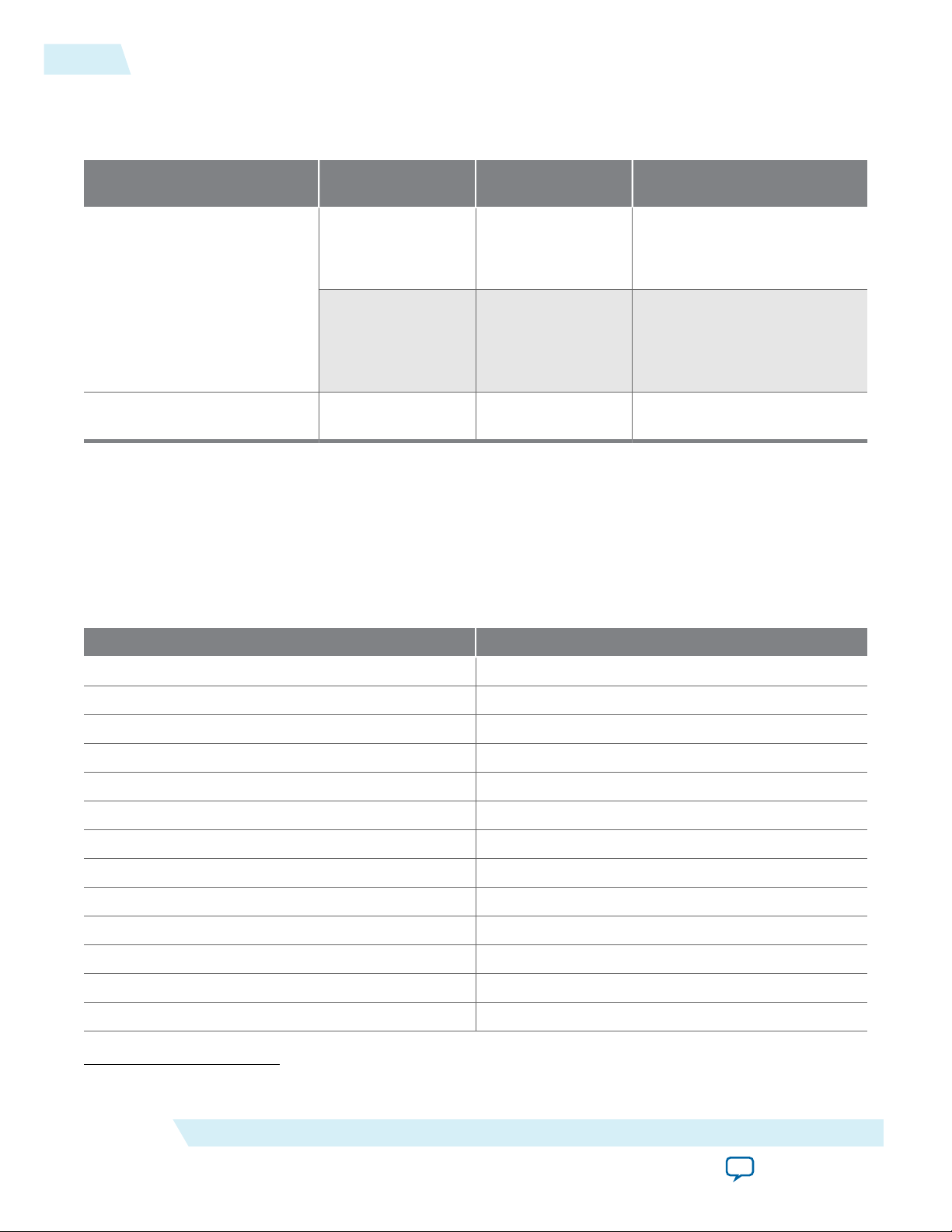
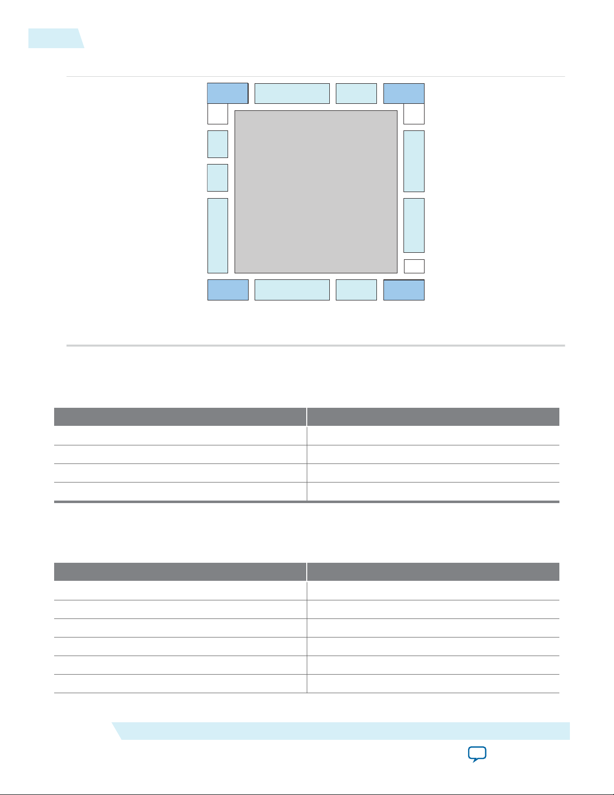
Figure 2-1: GCLK Network Sources for 10M02, 10M04, and 10M08 Devices
(1)
(1)
(1)
Global Clock Network Sources
CLK Pin GCLK
GCLK[16,17]
GCLK[16,18,19]
GCLK[15,18]
2-3
MAX 10 Clocking and PLL Architecture and Features
Send Feedback
Altera Corporation
Page 10
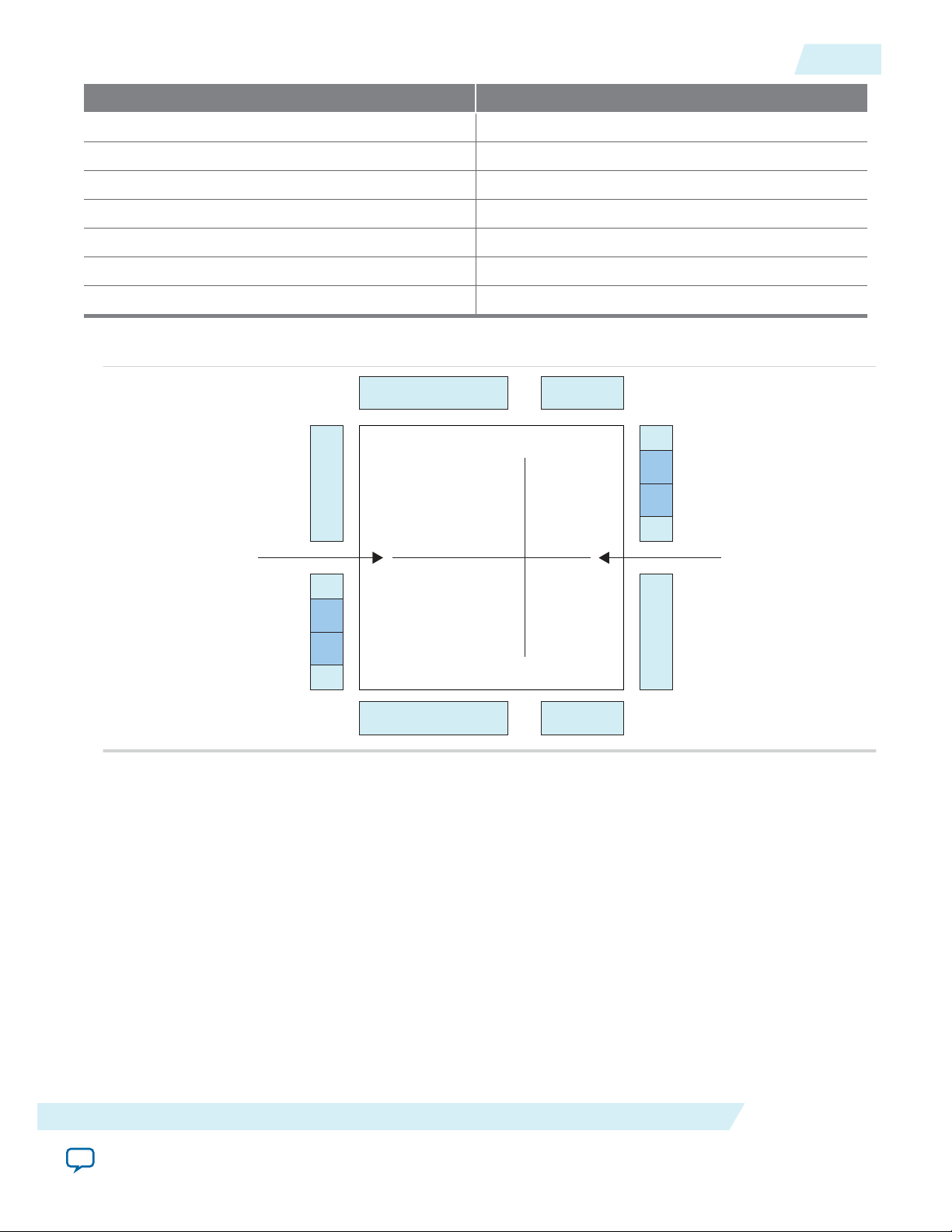
DPCLK2
DPCLK3
DPCLK0
DPCLK1
CLK[0,1][p,n] CLK[2,3][p,n]
GCLK[0..4] GCLK[5..9]
CLK[4,5][p,n]
CLK[6,7][p,n]
GCLK[15..19]
GCLK[10..14]
2-4
Global Clock Control Block
Figure 2-2: GCLK Network Sources for 10M16, 10M25, 10M40, and 10M50 Devices
UG-M10CLKPLL
2015.05.04
Global Clock Control Block
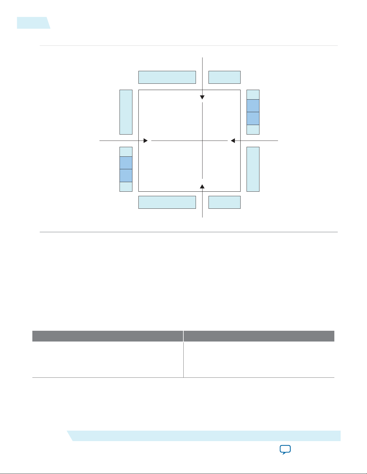
The clock control block drives GCLKs. The clock control blocks are located on each side of the device,
close to the dedicated clock input pins. GCLKs are optimized for minimum clock skew and delay.
The clock control block has the following functions:
• Dynamic GCLK clock source selection (not applicable for DPCLK pins and internal logic input)
• GCLK multiplexing
• GCLK network power down (dynamic enable and disable)
Table 2-3: Clock Control Block Inputs
Dedicated clock input pins Dedicated clock input pins can drive clocks or
Input Description
global signals, such as synchronous and asynchro‐
nous clears, presets, or clock enables onto given
GCLKs.
Altera Corporation
MAX 10 Clocking and PLL Architecture and Features
Send Feedback
Page 11
clkswitch (1)
Static Clock Select (3)
Static Clock
Select (3)
Internal Logic
Clock Control Block
DPCLK
clkselect[1..0] (2) Internal Logic (4)
inclk1
inclk0
CLK[n + 3]
CLK[n + 2]
CLK[n + 1]
CLK[n]
f
IN
C0
C1
C2
PLL
Global
Clock
Enable/
Disable
C3
C4
Notes:
(1) The clkswitch signal can either be set through the configuration file or dynamically set when using the manual PLL switchover
feature. The output of the multiplexer is the input clock (fIN) for the PLL.
(2) The clkselect[1..0] signals are fed by internal logic. You can use the clkselect[1..0] signals to dynamically select the clock source for
the GCLK when the device is in user mode. Only one PLL (applicable to PLLs on the same side) can be selected as the clock source to
the GCLK.
(3) The static clock select signals are set in the configuration file. Therefore, dynamic control when the device is in user mode is not
feasible.
(4) You can use internal logic to enable or disable the GCLK in user mode.
clkswitch (1)
inclk1
inclk0
f
IN
C0
C1
C2
PLL
C3
C4
UG-M10CLKPLL
2015.05.04
DPCLK pins DPCLK pins are bidirectional dual function pins that
PLL counter outputs PLL counter outputs can drive the GCLK.
Internal logic You can drive the GCLK through logic array
Figure 2-3: Clock Control Block
Global Clock Control Block
Input Description
are used for high fan-out control signals, such as
protocol signals, TRDY and IRDY signals for PCI via
the GCLK. Clock control blocks that have inputs
driven by DPCLK pins cannot drive PLL inputs.
routing to enable the internal logic elements (LEs)
to drive a high fan-out, low-skew signal path. Clock
control blocks that have inputs driven by internal
logic cannot drive PLL inputs.
2-5
Each MAX 10 device has a maximum of 20 clock control blocks. There are five clock control blocks on
each side of the device.
MAX 10 Clocking and PLL Architecture and Features
Send Feedback
Altera Corporation
Page 12
5
GCLK
Clock Input Pins
4
DPCLK
Internal Logic
Clock
Control
Block
5
PLL Outputs
5
4
Five Clock Control
Blocks on Each Side
of the Device
2-6
Global Clock Network Power Down
Each PLL generates five clock outputs through the c[4..0] counters. Two of these clocks can drive the
GCLK through a clock control block.
From the Clock Control Block Inputs table, only the following inputs can drive into any given clock
control block:
• Two dedicated clock input pins
• Two PLL counter outputs
• One DPCLK pin
• One source from internal logic
The output from the clock control block in turn feeds the corresponding GCLK. The GCLK can drive the
PLL input if the clock control block inputs are outputs of another PLL or dedicated clock input pins.
Normal I/O pins cannot drive the PLL input clock port.
Figure 2-4: Clock Control Block on Each Side of the Device
UG-M10CLKPLL
2015.05.04
Altera Corporation
Out of these five inputs to any clock control block, the two clock input pins and two PLL outputs are
dynamically selected to feed a GCLK. The clock control block supports static selection of the signal from
internal logic.
Related Information
• ALTCLKCTRL Parameters on page 5-1
• ALTCLKCTRL Ports and Signals on page 5-2
Global Clock Network Power Down
You can disable the MAX 10 GCLK (power down) by using both static and dynamic approaches. In the
static approach, configuration bits are set in the configuration file generated by the Quartus® II software,
which automatically disables unused GCLKs. The dynamic clock enable or disable feature allows internal
logic to control clock enable or disable of the GCLKs.
When a clock network is disabled, all the logic fed by the clock network is in an off-state, reducing the
overall power consumption of the device. This function is independent of the PLL and is applied directly
on the clock network.
You can set the input clock sources and the clkena signals for the GCLK multiplexers through the
ALTCLKCTRL IP core parameter editor in the Quartus II software.
MAX 10 Clocking and PLL Architecture and Features
Send Feedback
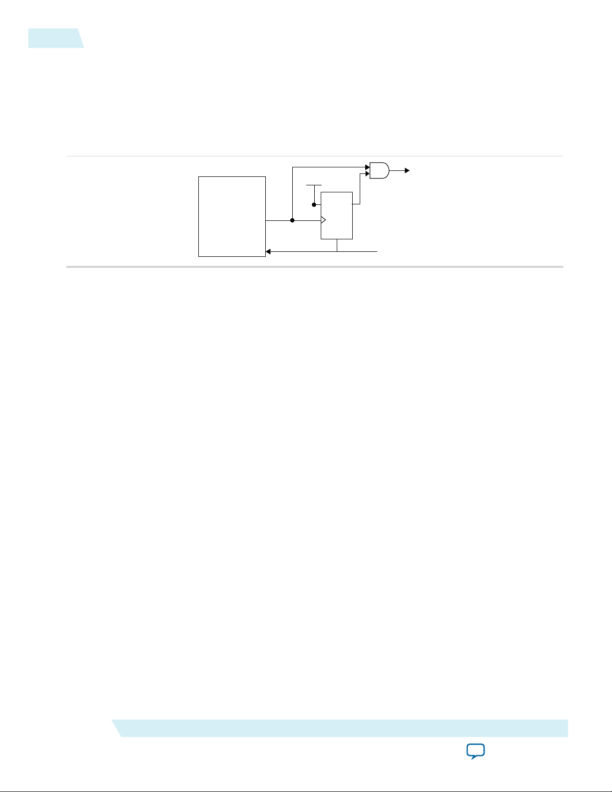
Page 13
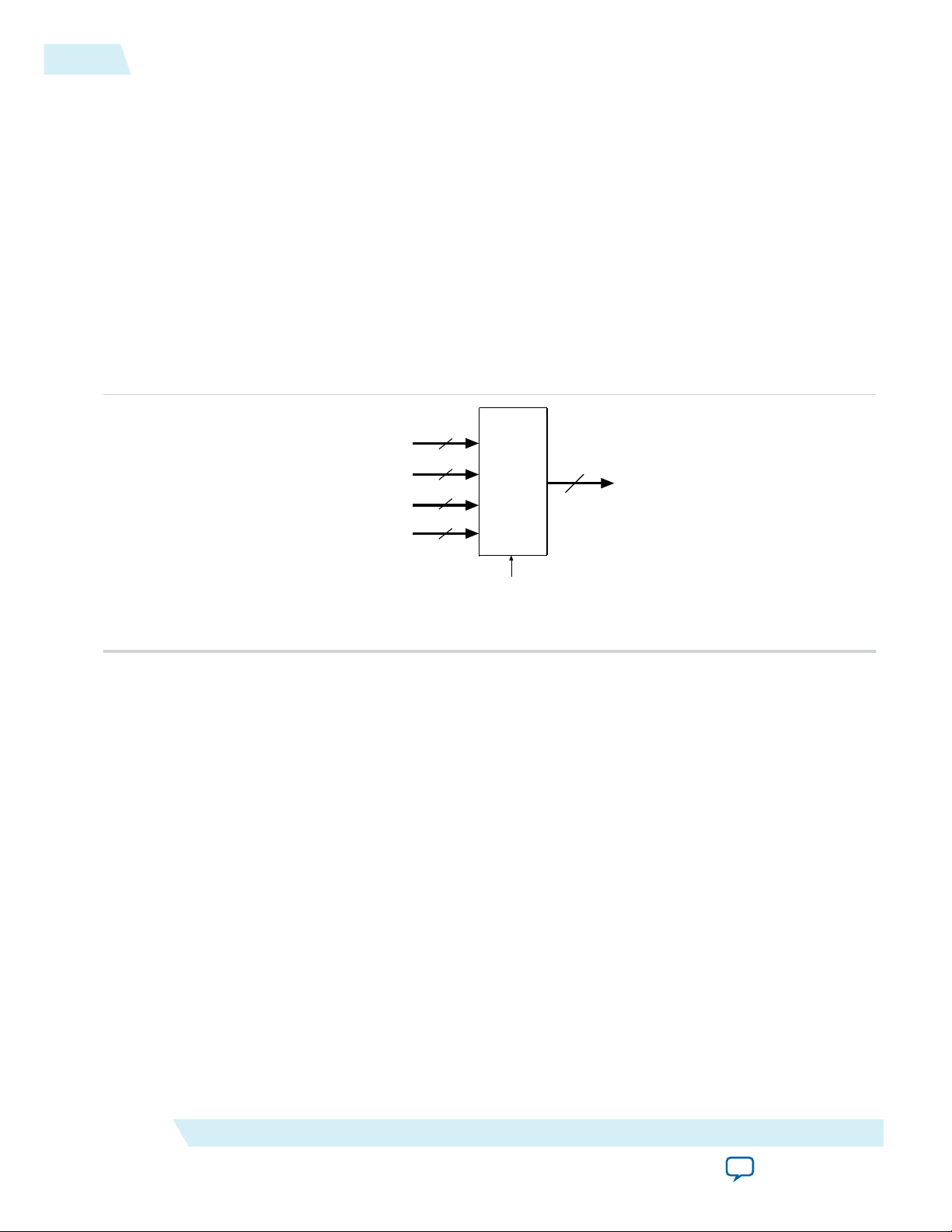
clkena clkena_out
clk_out
clkin
D Q
clkin
clkena
clk_out
UG-M10CLKPLL
2015.05.04
Related Information
• ALTCLKCTRL Parameters on page 5-1
• ALTCLKCTRL Ports and Signals on page 5-2
Clock Enable Signals
The MAX 10 devices support clkena signals at the GCLK network level. This allows you to gate off the
clock even when a PLL is used. After reenabling the output clock, the PLL does not need a resynchroniza‐
tion or relock period because the circuit gates off the clock at the clock network level. In addition, the PLL
can remain locked independent of the clkena signals because the loop-related counters are not affected.
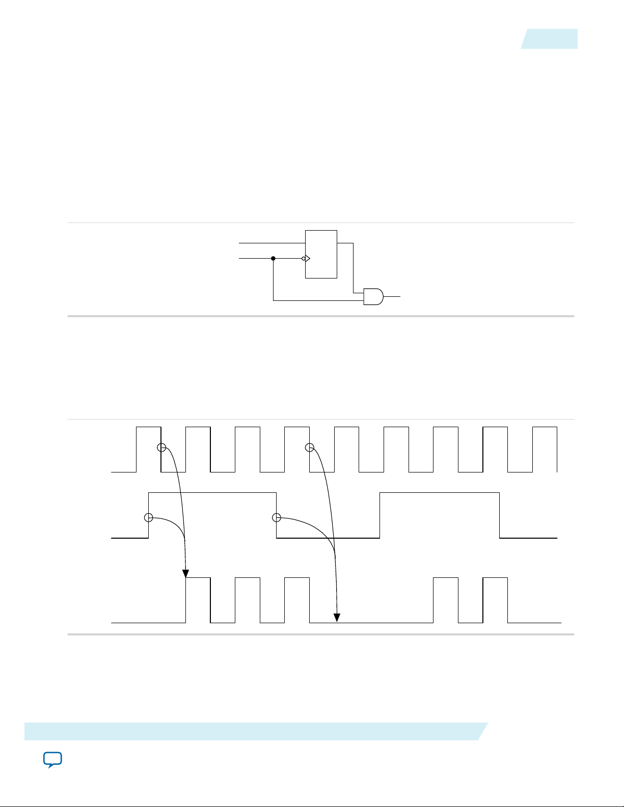
Figure 2-5: clkena Implementation
Clock Enable Signals
2-7
Note: The clkena circuitry controlling the C0 output of the PLL to an output pin is implemented with
two registers instead of a single register.
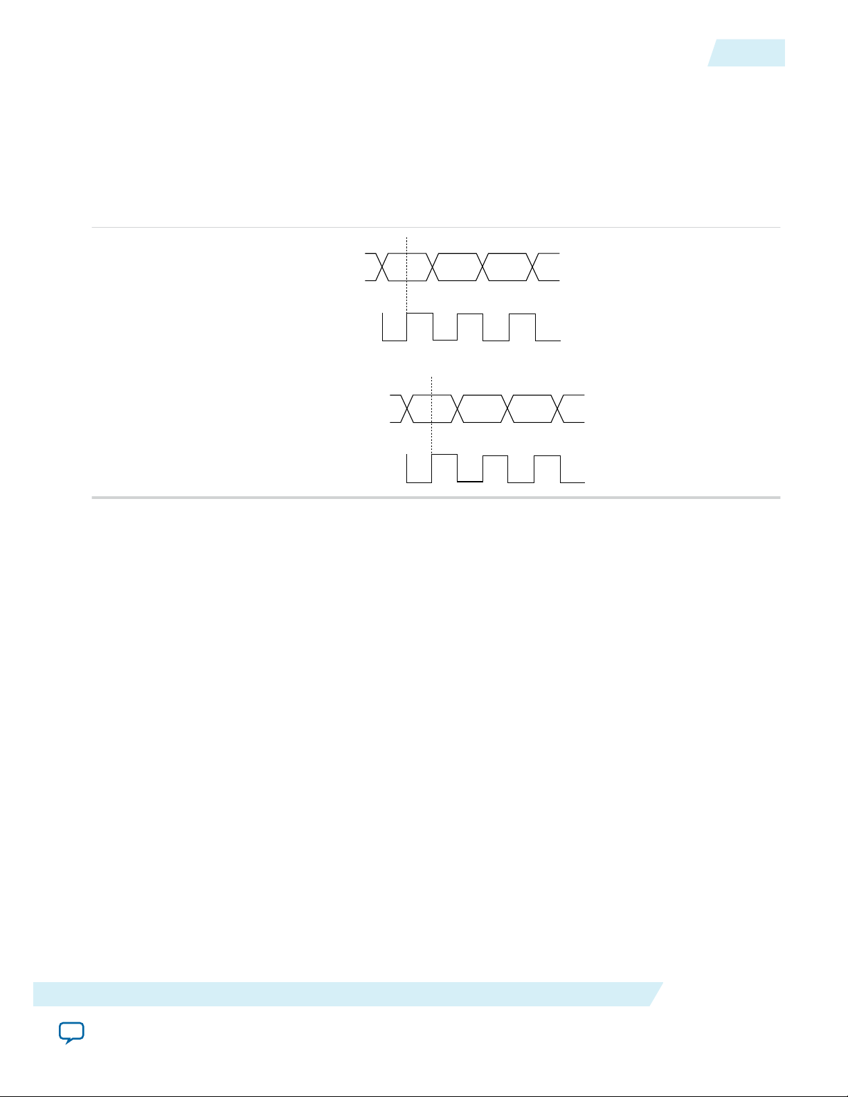
Figure 2-6: Example Waveform of clkena Implementation with Output Enable
The clkena signal is sampled on the falling edge of the clock (clkin). This feature is useful for
applications that require low power or sleep mode.
The clkena signal can also disable clock outputs if the system is not tolerant to frequency overshoot
during PLL resynchronization.
MAX 10 Clocking and PLL Architecture and Features
Send Feedback
Altera Corporation
Page 14
Clock
Switchover
Block
inclk0
inclk1
pfdena
clkswitch
clkbad0
clkbad1
activeclock
PFD
LOCK
circuit
lock
÷n
CP
LF
VCO
÷2 (1)
÷C0
÷C1
÷C2
÷C3
÷C4
÷M
PLL
output
mux
GCLKs
ADC clock (2)
8
8
GCLK
networks
No Compensation; ZDB Mode
Source-Synchronous; Normal Mode
VCO
Range
Detector
Notes:
(1) This is the VCO post-scale counter K.
(2) Only counter C0 of PLL1 and PLL3 can drive the ADC clock.
PLL
External clock output
4:1
Multiplexer
4:1
Multiplexer
CLKIN
2-8
Internal Oscillator Architecture and Features
Related Information
• Guideline: Clock Enable Signals on page 3-1
• ALTCLKCTRL Parameters on page 5-1
• ALTCLKCTRL Ports and Signals on page 5-2
Internal Oscillator Architecture and Features
MAX 10 devices have built-in internal ring oscillator with clock multiplexers and dividers. The internal
ring oscillator operates up to 232 MHz which is not accessible. This operating frequency further divides
down to slower frequencies.
By default internal oscillator is turned off in user mode. You can turn on the oscillator by asserting the
oscena signal in the Internal Oscillator IP core.
When the oscena input signal is asserted, the oscillator is enabled and the output can be routed to the
logic array through the clkout output signal. When the oscena signal is set low, the clkout signal is
constant high. You can analyze this delay using the TimeQuest timing analyzer.
PLLs Architecture and Features
UG-M10CLKPLL
2015.05.04
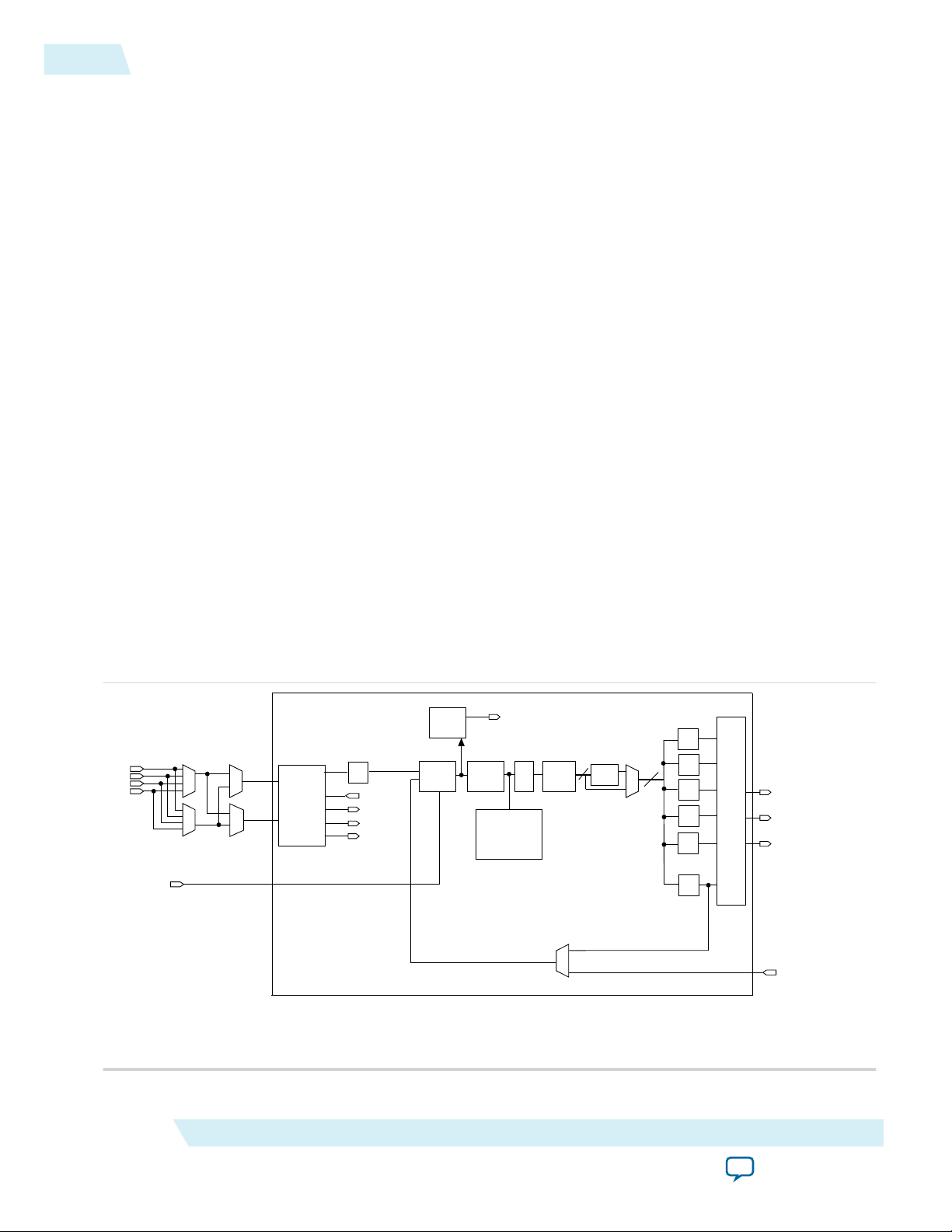
PLL Architecture
The main purpose of a PLL is to synchronize the phase and frequency of the voltage-controlled oscillator
(VCO) to an input reference clock.
Figure 2-7: MAX 10 PLL High-Level Block Diagram
Each clock source can come from any of the two or four clock pins located on the same side of the device
as the PLL.
Altera Corporation
MAX 10 Clocking and PLL Architecture and Features
Send Feedback
Page 15

UG-M10CLKPLL
2015.05.04
Phase-Frequency Detector (PFD)
PLL Architecture
2-9
The PFD has inputs from the feedback clock, fFB, and the input reference clock, f
. The PLL compares
REF
the rising edge of the input reference clock to a feedback clock using a PFD. The PFD produces an up or
down signal that determines whether the VCO needs to operate at a higher or lower frequency.
Charge Pump (CP)
If the charge pump receives a logic high on the up signal, current is driven into the loop filter. If the
charge pump receives a logic high on the down signal, current is drawn from the loop filter.
Loop Filter (LF)
The loop filter converts the up and down signals from the PFD to a voltage that is used to bias the VCO.
The loop filter filters out glitches from the charge pump and prevents voltage overshoot, which minimizes
jitter on the VCO.
Voltage-Controlled Oscillator (VCO)
The voltage from the charge pump determines how fast the VCO operates. The VCO is implemented as a
four-stage differential ring oscillator. A divide counter, M, is inserted in the feedback loop to increase the
VCO frequency, f
, above the input reference frequency, f
VCO
REF
.
The VCO frequency is determined using the following equation:
f
= f
VCO
× M = fIN × M/N ,
REF
where fIN is the input clock frequency to the PLL and N is the pre-scale counter.
The VCO frequency is a critical parameter that must be between 600 and 1,300 MHz to ensure proper
operation of the PLL. The Quartus II software automatically sets the VCO frequency within the
recommended range based on the clock output and phase shift requirements in your design.
Post-Scale Counters (C)
The VCO output can feed up to five post-scale counters (C0, C1, C2, C3, and C4). These post-scale counters
allow the PLL to produce a number of harmonically-related frequencies.
Internal Delay Elements
The MAX 10 PLLs have internal delay elements to compensate for routing on the GCLK networks and
I/O buffers. These internal delays are fixed.
PLL Outputs
The MAX 10 PLL supports up to 5 GCLK outputs and 1 dedicated external clock output. The output
frequency, f
, to the GCLK network or dedicated external clock output is determined using the
OUT
following equation:
f
= fIN/N and
REF
f
OUT
= f
VCO
/C = (f
× M)/C = (fIN × M)/(N × C),
REF
where C is the setting on the C0, C1, C2, C3, or C4 counter.
MAX 10 Clocking and PLL Architecture and Features
Send Feedback
Altera Corporation
Page 16

2-10
PLL Features
PLL Features
Table 2-4: MAX 10 PLL Features
Feature Support
C output counters 5
M, N, C counter sizes 1 to 512
Dedicated clock outputs 1 single-ended or 1 differential
Dedicated clock input pins 4 single-ended or 2 differential
Spread-spectrum input clock tracking Yes
PLL cascading Through GCLK
Source synchronous compensation Yes
No compensation mode Yes
Normal compensation Yes
Zero-delay buffer compensation Yes
Phase shift resolution Down to 96 ps increments
(3)
UG-M10CLKPLL
2015.05.04
(2)
(4)
Programmable duty cycle Yes
Output counter cascading Yes
Input clock switchover Yes
User mode reconfiguration Yes
Loss of lock detection Yes
4:1 multiplexer CLK input selection Yes
PLL Locations
The following figures show the physical locations of the PLLs. Every index represents one PLL in the
device. The physical locations of the PLLs correspond to the coordinates in the Quartus II Chip Planner.
(2)
C counters range from 1 through 512 if the output clock uses a 50% duty cycle. For any output clocks using a
non-50% duty cycle, the post-scale counters range from 1 through 256.
(3)
Only applicable if the input clock jitter is in the input jitter tolerance specifications.
(4)
The smallest phase shift is determined by the VCO period divided by eight. For degree increments, the
MAX 10 device family can shift all output frequencies in increments of at least 45°. Smaller degree
increments are possible depending on the frequency and divide parameters.
Altera Corporation
MAX 10 Clocking and PLL Architecture and Features
Send Feedback
Page 17
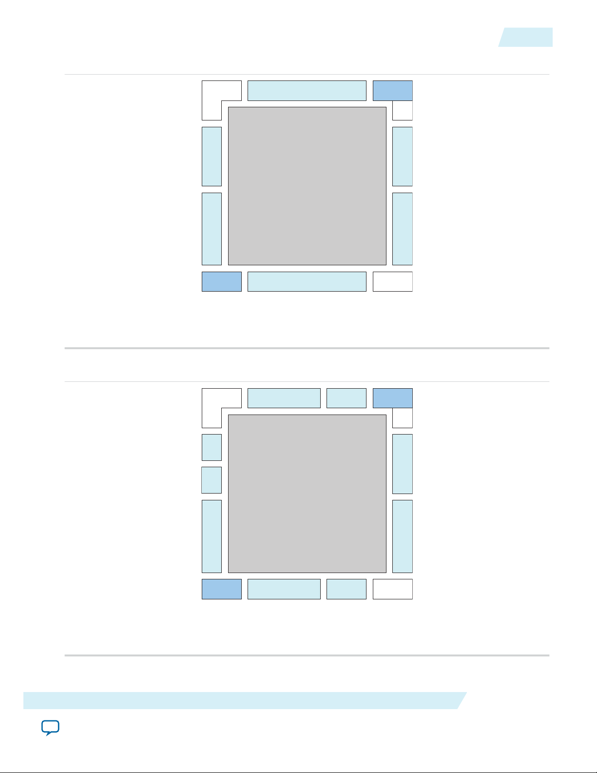
Bank 8
Bank 3
Bank 1Bank 2
Bank 6Bank 5
PLL 1 (1)
PLL 2 (2)
Notes:
(1) Available on all packages except V36 package.
(2) Available on U324 and V36packages only.
Bank 8
Bank 1A
Bank 2
Bank 6Bank 5
PLL 1 (1)
PLL 2 (2)Bank 7
Bank 3 Bank 4
Bank 1B
Notes:
(1) Available on all packages except V81 package.
(2) Available on F256, F484, U324, and V81 packages only.
UG-M10CLKPLL
2015.05.04
Figure 2-8: PLL Locations for 10M02 Device
PLL Locations
2-11
Figure 2-9: PLL Locations for 10M04 and 10M08 Devices
MAX 10 Clocking and PLL Architecture and Features
Send Feedback
Altera Corporation
Page 18
Bank 8
Bank 1A
Bank 2
Bank 6Bank 5
PLL 1
PLL 2 (1)Bank 7
Bank 3 Bank 4
Bank 1B
PLL 3 (1)
PLL 4 (1)
OCT
Note:
(1) Available on all packages except E144 and U169 packages.
2-12
Clock Pin to PLL Connections
Figure 2-10: PLL Locations for 10M16, 10M25, 10M40 and 10M50 Devices
UG-M10CLKPLL
2015.05.04
Clock Pin to PLL Connections
Table 2-5: MAX 10 Dedicated Clock Input Pin Connectivity to PLL
Dedicated Clock Pin PLL
CLK[0,1][p,n] PLL1, PLL3
CLK[2,3][p,n] PLL2, PLL4
CLK[4,5][p,n] PLL2, PLL3
CLK[6,7][p,n] PLL1, PLL4
PLL Counter to GCLK Connections
Table 2-6: MAX 10 PLL Counter Connectivity to the GCLK Networks
PLL Counter Output GCLK
PLL1_C0 GCLK[0,3,15,18]
PLL1_C1 GCLK[1,4,16,19]
PLL1_C2 GCLK[0,2,15,17]
PLL1_C3 GCLK[1,3,16,18]
PLL1_C4 GCLK[2,4,17,19]
PLL2_C0 GCLK[5,8,10,13]
Altera Corporation
MAX 10 Clocking and PLL Architecture and Features
Send Feedback
Page 19

UG-M10CLKPLL
2015.05.04
PLL Control Signals
PLL Counter Output GCLK
PLL2_C1 GCLK[6,9,11,14]
PLL2_C2 GCLK[5,7,10,12]
PLL2_C3 GCLK[6,8,11,13]
PLL2_C4 GCLK[7,9,12,14]
PLL3_C0
PLL3_C1
PLL3_C2
PLL3_C3
PLL3_C4
PLL4_C0
PLL4_C1
PLL4_C2
PLL4_C3
PLL4_C4
(5)
(5)
(5)
(5)
(5)
(5)
(5)
(5)
(5)
(5)
GCLK[0,3,10,13]
GCLK[1,4,11,14]
GCLK[0,2,10,12]
GCLK[1,3,11,13]
GCLK[2,4,12,14]
GCLK[5,8,15,18]
GCLK[6,9,16,19]
GCLK[5,7,15,17]
GCLK[6,8,16,18]
GCLK[7,9,17,19]
2-13
PLL Control Signals
You can use the following three signals to observe and control the PLL operation and resynchronization.
pfdena
Use the pfdena signal to maintain the last locked frequency so that your system has time to store its
current settings before shutting down.
The pfdena signal controls the PFD output with a programmable gate. The PFD circuit is enabled by
default. When the PFD circuit is disabled, the PLL output does not depend on the input clock, and tends
to drift outside of the lock window.
areset
The areset signal is the reset or resynchronization input for each PLL. The device input pins or internal
logic can drive these input signals.
When you assert the areset signal, the PLL counters reset, clearing the PLL output and placing the PLL
out of lock. The VCO is then set back to its nominal setting. When the areset signal is deasserted, the
PLL resynchronizes to its input as it relocks.
The assertion of the areset signal does not disable the VCO, but instead resets the VCO to its nominal
value. The only time that the VCO is completely disabled is when you do not have a PLL instantiated in
your design.
(5)
This only applies to 10M16, 10M25, 10M40, and 10M50 devices.
MAX 10 Clocking and PLL Architecture and Features
Send Feedback
Altera Corporation
Page 20
DFF
D
Q
PLL
locked
locked
areset
V
CC
2-14
Clock Feedback Modes
locked
The locked output indicates that the PLL has locked onto the reference clock and the PLL clock outputs
are operating at the desired phase and frequency set in the ALTPLL IP core parameter editor.
Altera recommends using the areset and locked signals in your designs to control and observe the status
of your PLL. This implementation is illustrated in the following figure.
Figure 2-11: locked Signal Implementation
Note: If you use the SignalTap® II tool to probe the locked signal before the D flip-flop, the locked
signal goes low only when areset is deasserted. If the areset signal is not enabled, the extra logic
is not implemented in the ALTPLL IP core.
UG-M10CLKPLL
2015.05.04
Related Information
• Guideline: PLL Control Signals on page 3-2
• PLL Control Signals Parameter Settings on page 6-2
• ALTPLL Ports and Signals on page 6-6
Clock Feedback Modes
The MAX 10 PLLs support up to four different clock feedback modes. Each mode allows clock multiplica‐
tion and division, phase shifting, and programmable duty cycle.
The PLL fully compensates input and output delays only when you use the dedicated clock input pins
associated with a given PLL as the clock sources.
For example, when using PLL1 in normal mode, the clock delays from one of the following clock input
pins to the PLL and the PLL clock output-to-destination register are fully compensated:
• CLK0
• CLK1
• CLK2
• CLK3
When driving the PLL using the GCLK network, the input and output delays might not be fully
compensated in the Quartus II software.
Altera Corporation
Related Information
Operation Modes Parameter Settings on page 6-1
MAX 10 Clocking and PLL Architecture and Features
Send Feedback
Page 21
Data pin
PLL reference
clock at input pin
Data at register
Clock at register
UG-M10CLKPLL
2015.05.04
Source Synchronous Mode
If the data and clock arrive at the same time at the input pins, the phase relationship between the data and
clock remains the same at the data and clock ports of any I/O element input register.
You can use this mode for source synchronous data transfers. Data and clock signals at the I/O element
experience similar buffer delays as long as both signals use the same I/O standard.
Figure 2-12: Example of Phase Relationship Between Clock and Data in Source Synchronous Mode
Source Synchronous Mode
2-15
Source synchronous mode compensates for clock network delay, including any difference in delay
between the following two paths:
• Data pin to I/O element register input
• Clock input pin to the PLL PFD input
For all data pins clocked by a source synchronous mode PLL, set the input pin to the register delay chain
in the I/O element to zero in the Quartus II software. All data pins must use the PLL COMPENSATED
logic option in the Quartus II software.
No Compensation Mode
In no compensation mode, the PLL does not compensate for any clock networks. This mode provides
better jitter performance because clock feedback into the PFD does not pass through as much circuitry.
Both the PLL internal and external clock outputs are phase-shifted with respect to the PLL clock input.
MAX 10 Clocking and PLL Architecture and Features
Altera Corporation
Send Feedback
Page 22
PLL Reference
Clock at the Input Pin
PLL Clock at the
Register Clock Port
(1), (2)
External PLL Clock
Outputs (2)
Phase Aligned
Notes:
(1) Internal clocks fed by the PLL are phase-aligned to each other.
(2) The PLL clock outputs can lead or lag the PLL input clocks. The PLL clock outputs lag the
PLL input clocks depending on the routine delays.
PLL Reference
Clock at the Input pin
PLL Clock at the
Register Clock Port
External PLL Clock
Outputs (1)
Phase Aligned
Note:
(1) The external clock output can lead or lag the PLL internal clock signals.
2-16
Normal Mode
Figure 2-13: Example of Phase Relationship Between the PLL Clocks in No Compensation Mode
UG-M10CLKPLL
2015.05.04
Normal Mode
In normal mode, the PLL fully compensates the delay introduced by the GCLK network. An internal clock
in normal mode is phase-aligned to the input clock pin. In this mode, the external clock output pin has a
phase delay relative to the input clock pin. The Quartus II software timing analyzer reports any phase
difference between the two.
Figure 2-14: Example of Phase Relationship Between the PLL Clocks in Normal Compensation Mode
Altera Corporation
MAX 10 Clocking and PLL Architecture and Features
Send Feedback
Page 23

PLL Reference Clock
at the Input Pin
PLL Clock
at the Register Clock Port
External PLL Clock Output
at the Output Pin
Phase Aligned
UG-M10CLKPLL
2015.05.04
Zero-Delay Buffer Mode
In zero-delay buffer (ZDB) mode, the external clock output pin is phase-aligned with the clock input pin
for zero delay through the device. When using this mode, use the same I/O standard for the input clock
and output clocks to ensure clock alignment at the input and output pins.
Figure 2-15: Example of Phase Relationship Between the PLL Clocks in ZDB Mode
Zero-Delay Buffer Mode
2-17
PLL External Clock Output
Each PLL in the MAX 10 devices supports one single-ended clock output or one differential clock output.
Only the C0 output counter can feed the dedicated external clock outputs without going through the
GCLK. Other output counters can feed other I/O pins through the GCLK.
MAX 10 Clocking and PLL Architecture and Features
Send Feedback
Altera Corporation
Page 24
C0
C1
C2
C4
C3
PLL #
clkena 1 (1)
clkena 0 (1)
PLL #_CLKOUTp (2)
PLL #_CLKOUTn (2)
Notes:
(1) These external clock enable signals are available only when using the ALTCLKCTRL IP core.
(2) PLL#_CLKOUTp and PLL#_CLKOUTn pins are dual-purpose I/O pins that you can use as one single-ended
or one differential clock output.
2-18
PLL External Clock Output
Figure 2-16: PLL External Clock Output
UG-M10CLKPLL
2015.05.04
Each pin of a differential output pair is 180° out of phase. To implement the 180° out-of-phase pin in a
pin pair, the Quartus II software places a NOT gate in the design into the I/O element.
The clock output pin pairs support the following I/O standards:
• Same I/O standard as the standard output pins (in the top and bottom banks)
• LVDS
• LVPECL
• Differential high-speed transceiver logic (HSTL)
• Differential SSTL
The MAX 10 PLLs can drive out to any regular I/O pin through the GCLK. You can also use the external
clock output pins as general-purpose I/O pins if you do not require any external PLL clocking.
Related Information
MAX 10 General Purpose I/O User Guide
Provides more information about the I/O standards supported by the PLL clock output pins.
Altera Corporation
MAX 10 Clocking and PLL Architecture and Features
Send Feedback
Page 25

UG-M10CLKPLL
2015.05.04
ADC Clock Input from PLL
Only the C0 output counter from PLL1 and PLL3 can drive the ADC clock.
Counter C0 has dedicated path to the ADC clock input.
Spread-Spectrum Clocking
The MAX 10 devices allow a spread-spectrum input with typical modulation frequencies. However, the
device cannot automatically detect that the input is a spread-spectrum signal. Instead, the input signal
looks like deterministic jitter at the input of the PLL.
The MAX 10 PLLs can track a spread-spectrum input clock if the input signal meets the following
conditions:
• The input signal is within the input jitter tolerance specifications.
• The modulation frequency of the input clock is below the PLL bandwidth as specified in the Fitter
report.
MAX 10 devices cannot generate spread-spectrum signals internally.
PLL Programmable Parameters
ADC Clock Input from PLL
2-19
Programmable Duty Cycle
The programmable duty cycle allows PLLs to generate clock outputs with a variable duty cycle. This
feature is supported on the PLL post-scale counters.
The duty cycle setting is achieved by a low and high time-count setting for the post-scale counters. To
determine the duty cycle choices, the Quartus II software uses the frequency input and the required
multiply or divide rate.
The post-scale counter value determines the precision of the duty cycle. The precision is defined as 50%
divided by the post-scale counter value. For example, if the C0 counter is 10, steps of 5% are possible for
duty cycle choices between 5 to 90%.
Combining the programmable duty cycle with programmable phase shift allows the generation of precise
nonoverlapping clocks.
Related Information
Post-Scale Counters (C0 to C4) on page 4-11
Provides more information about configuring the duty cycle of the post-scale counters in real time.
Programmable Bandwidth
The PLL bandwidth is the measure of the PLL’s ability to track the input clock and its associated jitter.
The MAX 10 PLLs provide advanced control of the PLL bandwidth using the programmable characteris‐
tics of the PLL loop, including loop filter and charge pump. The 3-dB frequency of the closed-loop gain in
the PLL determines the PLL bandwidth. The bandwidth is approximately the unity gain point for open
loop PLL response.
Related Information
• Programmable Bandwidth with Advanced Parameters on page 4-10
MAX 10 Clocking and PLL Architecture and Features
Send Feedback
Altera Corporation
Page 26
2-20
Programmable Phase Shift
• Charge Pump and Loop Filter on page 4-13
Provides more information about the PLL components to update PLL bandwidth in real time.
• Programmable Bandwidth Parameter Settings on page 6-2
Programmable Phase Shift
The MAX 10 devices use phase shift to implement clock delays. You can phase shift the output clocks
from the MAX 10 PLLs using one of the following methods:
• Fine resolution using VCO phase taps
• Coarse resolution using counter starting time
The VCO phase output and counter starting time are the most accurate methods of inserting delays.
These methods are purely based on counter settings, which are independent of process, voltage, and
temperature.
The MAX 10 devices support dynamic phase shifting of VCO phase taps only. The phase shift is configu‐
rable for any number of times. Each phase shift takes about one scanclk cycle, allowing you to implement
large phase shifts quickly.
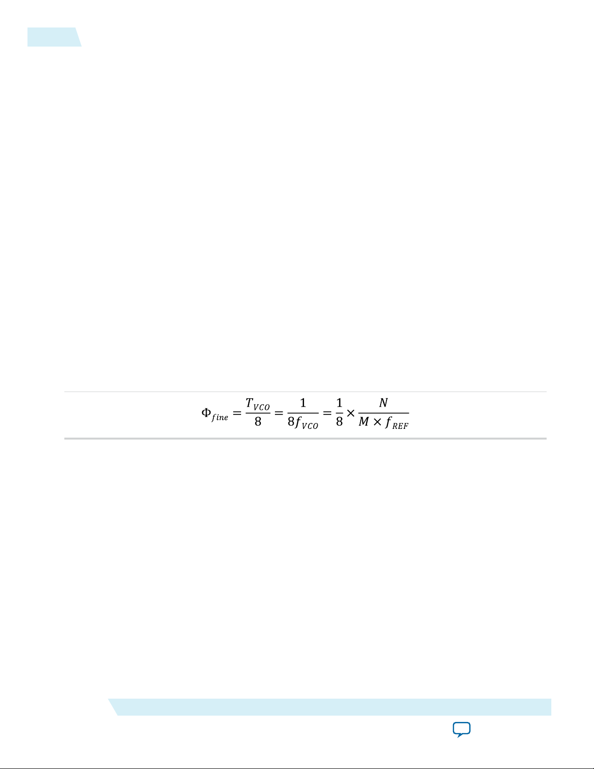
Fine Resolution Phase Shift
Fine resolution phase shifts are implemented by allowing any of the output counters (C[4..0]) or the M
counter to use any of the eight phases of the VCO as the reference clock. This allows you to adjust the
delay time with a fine resolution. The following equation shows the minimum delay time that you can
insert using this method.
UG-M10CLKPLL
2015.05.04
Figure 2-17: Fine Resolution Phase Shift Equation
f
in this equation is the input reference clock frequency
REF
For example, if f
is 100 MHz, N = 1, and M = 8, then f
REF
= 800 MHz, and Φ
VCO
= 156.25 ps. The PLL
fine
operating frequency defines this phase shift, a value that depends on the reference clock frequency and
counter settings.
The following figure shows an example of phase shift insertion using the fine resolution through VCO
phase taps method. The eight phases from the VCO are shown and labeled for reference.
Altera Corporation
MAX 10 Clocking and PLL Architecture and Features
Send Feedback
Page 27

t
d0-1
t
d0-2
1/8 t
VCO
t
VCO
0
90
135
180
225
270
315
CLK0
CLK1
CLK2
45
UG-M10CLKPLL
2015.05.04
Figure 2-18: Example of Delay Insertion Using VCO Phase Output and Counter Delay Time
Programmable Phase Shift
2-21
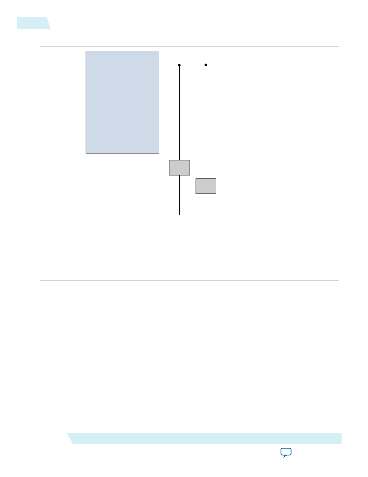
The observations in this example are as follows:
• CLK0 is based on 0° phase from the VCO and has the C value for the counter set to one.
• CLK1 signal is divided by four, two VCO clocks for high time and two VCO clocks for low time. CLK1 is
based on the 135° phase tap from the VCO and has the C value for the counter set to one.
• CLK2 signal is also divided by four. In this case, the two clocks are offset by 3 Φ
. CLK2 is based on the
fine
0° phase from the VCO but has the C value for the counter set to three. This creates a delay of two
Φ
(two complete VCO periods).
coarse
Coarse Resolution Phase Shift
Coarse resolution phase shifts are implemented by delaying the start of the counters for a predetermined
number of counter clocks.
Figure 2-19: Coarse Resolution Phase Shift Equation
C in this equation is the count value set for the counter delay time—the initial setting in the PLL usage
section of the compilation report in the Quartus II software. If the initial value is 1, C – 1 = 0° phase shift.
Related Information
• Dynamic Phase Configuration Implementation on page 4-15
• Dynamic Phase Configuration Counter Selection on page 4-16
• Dynamic Phase Configuration with Advanced Parameters on page 4-16
MAX 10 Clocking and PLL Architecture and Features
Send Feedback
Altera Corporation
Page 28

2-22
Clock Switchover
• Dynamic Phase Configuration Parameter Settings on page 6-4
Provides more information about the ALTPLL IP core parameter settings in the Quartus II software.
• ALTPLL_RECONFIG Parameters on page 7-1
Provides more information about the ALTPLL_RECONFIG IP core parameter settings in the Quartus
II software.
Clock Switchover
The clock switchover feature allows the PLL to switch between two reference input clocks. Use this feature
for clock redundancy or for a dual-clock domain application where a system turns on the redundant clock
if the previous clock stops running. The design can perform clock switchover automatically when the
clock is no longer toggling or based on a user-controlled signal, clkswitch.
The following clock switchover modes are supported in MAX 10 PLLs:
• Automatic switchover—The clock sense circuit monitors the current reference clock. If the current
reference clock stops toggling, the reference clock automatically switches to inclk0 or inclk1 clock.
• Manual clock switchover—The clkswitch signal controls the clock switchover. When the clkswitch
signal goes from logic low to high, and stays high for at least three clock cycles, the reference clock to
the PLL switches from inclk0 to inclk1, or vice-versa.
• Automatic switchover with manual override—This mode combines automatic switchover and manual
clock switchover. When the clkswitch signal goes high, it overrides the automatic clock switchover
function. As long as the clkswitch signal is high, any further switchover action is blocked.
UG-M10CLKPLL
2015.05.04
Related Information
• Guideline: Clock Switchover on page 3-3
• Clock Switchover Parameter Settings on page 6-3
Automatic Clock Switchover
The MAX 10 PLLs support a fully configurable clock switchover capability.
Altera Corporation
MAX 10 Clocking and PLL Architecture and Features
Send Feedback
Page 29

Switchover
State
Machine
Clock
Sense
N Counter
PFD
clkswitch
(Provides Manual
Switchover Support)
activeclock
clkbad1
clkbad0
muxout
inclk0
inclk1
refclk
fbclk
clksw
UG-M10CLKPLL
2015.05.04
Figure 2-20: Automatic Clock Switchover Circuit Block Diagram
Automatic Clock Switchover
This figure shows a block diagram of the automatic switchover circuit built into the PLL.
2-23
When the current reference clock is not present, the clock sense block automatically switches to the
backup clock for PLL reference. You can select a clock source at the backup clock by connecting it to the
inclk1 port of the PLL in your design.
The clock switchover circuit also sends out three status signals—clkbad[0], clkbad[1], and
activeclock—from the PLL to implement a custom switchover circuit in the logic array.
In automatic switchover mode, the clkbad[0] and clkbad[1] signals indicate the status of the two clock
inputs. When the clkbad[0] and clkbad[1] signals are asserted, the clock sense block detects that the
corresponding clock input has stopped toggling. These two signals are not valid if the frequency difference
between inclk0 and inclk1 is greater than 20%.
The activeclock signal indicates which of the two clock inputs (inclk0 or inclk1) is selected as the
reference clock to the PLL. When the frequency difference between the two clock inputs is more than
20%, the activeclock signal is the only valid status signal.
Note:
Glitches in the input clock may cause the frequency difference between the input clocks to be more
than 20%.
When the current reference clock to the PLL stops toggling, use the switchover circuitry to automatically
switch from inclk0 to inclk1 that runs at the same frequency. This automatic switchover can switch
back and forth between the inclk0 and inclk1 clocks any number of times when one of the two clocks
fails and the other clock is available.
For example, in applications that require a redundant clock with the same frequency as the reference
clock, the switchover state machine generates a signal (clksw) that controls the multiplexer select input.
In this case, inclk1 becomes the reference clock for the PLL.
MAX 10 Clocking and PLL Architecture and Features
Send Feedback
Altera Corporation
Page 30

inclk0
inclk1
muxout
clkbad0
clkbad1
(1)
activeclock
Note:
(1) Switchover is enabled on the falling edge of inclk0 or inclk1, depending on which clock is available. In this figure,
switchover is enabled on the falling edge of inclk1.
2-24
Automatic Switchover with Manual Override
When using automatic clock switchover mode, the following requirements must be satisfied:
• Both clock inputs must be running when the FPGA is configured.
• The period of the two clock inputs differ by no more than 20%.
If the current clock input stops toggling while the other clock is also not toggling, switchover is not
initiated and the clkbad[0..1] signals are not valid. If both clock inputs do not have the same frequency,
but their period difference is within 20%, the clock sense block detects when a clock stops toggling.
However, the PLL might lose lock after the switchover completes and needs time to relock.
Note: Altera recommends resetting the PLL using the areset signal to maintain the phase relationships
between the PLL input and output clocks when using clock switchover.
Figure 2-21: Example of Automatic Switchover After Loss of Clock Detection
This figure shows an example waveform of the switchover feature in automatic switchover mode. In this
example, the inclk0 signal remains low. After the inclk0 signal remains low for approximately two clock
cycles, the clock sense circuitry drives the clkbad[0] signal high. Since the reference clock signal is not
toggling, the switchover state machine controls the multiplexer through the clksw signal to switch to the
backup clock, inclk1.
UG-M10CLKPLL
2015.05.04
Automatic Switchover with Manual Override
In automatic switchover with manual override mode, you can use the clkswitch signal for user- or
system-controlled switch conditions. You can use this mode for same-frequency switchover, or to switch
Altera Corporation
between inputs of different frequencies.
For example, if inclk0 is 66 MHz and inclk1 is 200 MHz, you must control the switchover using the
clkswitch signal. The automatic clock sense circuitry cannot monitor clock input (inclk0 and inclk1)
frequencies with a frequency difference of more than 20%.
This feature is useful when clock sources originate from multiple cards on the backplane, requiring a
system-controlled switchover between frequencies of operation.
MAX 10 Clocking and PLL Architecture and Features
Send Feedback
Page 31

inclk0
inclk1
muxout
clkswitch
activeclock
clkbad0
clkbad1
To initiate a manual clock switchover event,
both inclk0 and inclk1 must be running when
the clkswitch signal goes high.
UG-M10CLKPLL
2015.05.04
Manual Clock Switchover
2-25
You must choose the backup clock frequency and set the M, N, and C counters so that the VCO operates
within the recommended frequency range.
The following figure shows a clock switchover waveform controlled by the clkswitch signal. In this case,
both clock sources are functional and inclk0 is selected as the reference clock. The clkswitch signal goes
high, which starts the switchover sequence. On the falling edge of inclk0, the counter’s reference clock,
muxout, is gated off to prevent clock glitching. On the falling edge of inclk1, the reference clock
multiplexer switches from inclk0 to inclk1 as the PLL reference. The activeclock signal is asserted to
indicate the clock that is currently feeding the PLL, which is inclk1.
In automatic override with manual switchover mode, the activeclock signal mirrors the clkswitch
signal. Since both clocks are still functional during the manual switch, neither clkbad signal goes high.
Because the switchover circuit is positive-edge sensitive, the falling edge of the clkswitch signal does not
cause the circuit to switch back from inclk1 to inclk0. When the clkswitch signal goes high again, the
process repeats.
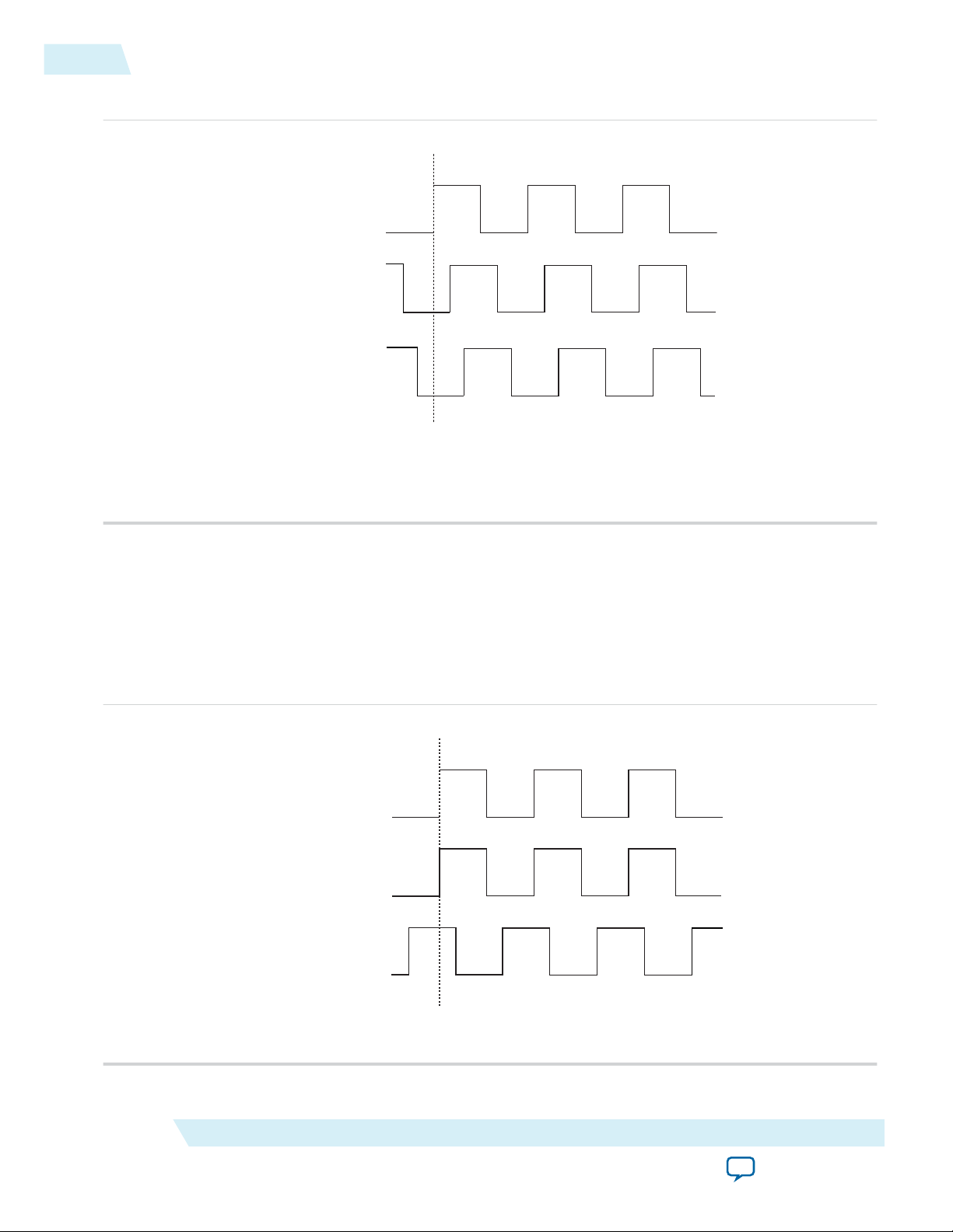
Figure 2-22: Example of Clock Switchover Using the
clkswitch signal and automatic switch work only if the clock being switched to is available. If the
The
clkswitch
clock is not available, the state machine waits until the clock is available.
(Manual) Control
Manual Clock Switchover
In manual clock switchover mode, the clkswitch signal controls whether inclk0 or inclk1 is selected as
the input clock to the PLL. By default, inclk0 is selected.
A clock switchover event is initiated when the clkswitch signal transitions from logic low to logic high,
and is being held high for at least three inclk cycles. You must bring the clkswitch signal back to low
again to perform another switchover event. If you do not require another switchover event, you can leave
the clkswitch signal in a logic high state after the initial switch. Pulsing the clkswitch signal high for at
least three inclk cycles performs another switchover event.
MAX 10 Clocking and PLL Architecture and Features
Send Feedback
Altera Corporation
Page 32

C0
C1
C2
C3
C4
VCO Output
VCO Output
VCO Output
VCO Output
VCO Output
VCO Output
2-26
PLL Cascading
If inclk0 and inclk1 have different frequencies and are always running, the minimum amount of time
for which clkswitch signal is high must be greater than or equal to three of the slower-frequency inclk0
and inclk1 cycles.
PLL Cascading
Related Information
Guideline: PLL Cascading on page 3-3
PLL-to-PLL Cascading
Two PLLs are cascaded to each other through the clock network. If your design cascades PLLs, the source
(upstream) PLL must have a low-bandwidth setting and the destination (downstream) PLL must have a
high-bandwidth setting.
Counter-to-Counter Cascading
The MAX 10 PLLs support post-scale counter cascading to create counters larger than 512. This is
implemented by feeding the output of one C counter into the input of the next C counter.
Figure 2-23: Counter-to-Counter Cascading
UG-M10CLKPLL
2015.05.04
Altera Corporation
When cascading counters to implement a larger division of the high-frequency VCO clock, the cascaded
counters behave as one counter with the product of the individual counter settings.
For example, if C0 = 4 and C1 = 2, the cascaded value is C0 x C1 = 8.
The Quartus II software automatically sets all the post-scale counter values for cascading in the configura‐
tion file. Post-scale counter cascading cannot be performed using PLL reconfiguration.
PLL Reconfiguration
The PLLs use several divide counters and different VCO phase taps to perform frequency synthesis and
phase shifts. In MAX 10 PLLs, you can reconfigure both counter settings and phase shift the PLL output
clock in real time. You can also change the charge pump and loop filter components, which dynamically
affects the PLL bandwidth.
MAX 10 Clocking and PLL Architecture and Features
Send Feedback
Page 33

/C4 /C3 /C2 /C1 /C0 /M /N
scanclk
scandone
scandata
LF/K/CP
configupdate
inclk
PFD VCO
F
VCO
scanclkena
scandataout
from M counter
from N counter
UG-M10CLKPLL
2015.05.04
PLL Reconfiguration
2-27
The following PLL components are configurable in real time:
• Pre-scale counter (N)
• Feedback counter (M)
• Post-scale output counters (C0-C4)
• Charge pump current (ICP)
• Loop filter components (R, C)
You can use these PLL components to update the following settings in real time without reconfiguring the
entire FPGA:
• Output clock frequency
• PLL bandwidth
• Phase shift
The ability to reconfigure the PLL in real time is useful in applications that may operate in multiple
frequencies. It is also useful in prototyping environments, allowing you to sweep PLL output frequencies
and dynamically adjust the output clock phase.
For instance, a system generating test patterns is required to generate and send patterns at 75 or 150 MHz,
depending on the requirements of the device under test. Reconfiguring the PLL components in real time
allows you to switch between two such output frequencies in a few microseconds.
You can also use this feature to adjust clock-to-out (tCO) delays in real time by changing the PLL output
clock phase shift. This approach eliminates the need to regenerate a configuration file with the new PLL
settings.
Figure 2-24: PLL Reconfiguration Scan Chain
This figure shows the dynamic adjustment of the PLL counter settings by shifting their new settings into a
serial shift register chain or scan chain. Serial data shifts to the scan chain via the scandata port, and shift
registers are clocked by scanclk. The maximum scanclk frequency is 100 MHz. After shifting the last bit
of data, asserting the configupdate signal for at least one scanclk clock cycle synchronously updates the
PLL configuration bits with the data in the scan registers.
MAX 10 Clocking and PLL Architecture and Features
Send Feedback
Altera Corporation
Page 34

2-28
PLL Reconfiguration
UG-M10CLKPLL
2015.05.04
The counter settings are updated synchronously to the clock frequency of the individual counters.
Therefore, not all counters update simultaneously.
The dynamic reconfiguration scheme uses configuration files, such as the Hexadecimal-format file (.hex)
or the Memory Initialization file (.mif). These files are used together with the ALTPLL_RECONFIG IP
core to perform the dynamic reconfiguration.
Related Information
• Guideline: .mif Streaming in PLL Reconfiguration on page 3-4
• PLL Dynamic Reconfiguration Implementation on page 4-10
• PLL Dynamic Reconfiguration Parameter Settings on page 6-4
Provides more information about the ALTPLL IP core parameter settings in the Quartus II software.
• ALTPLL_RECONFIG Parameters on page 7-1
Provides more information about the ALTPLL_RECONFIG IP core parameter settings in the Quartus
II software.
Altera Corporation
MAX 10 Clocking and PLL Architecture and Features
Send Feedback
Page 35

MAX 10 Clocking and PLL Design
www.altera.com
101 Innovation Drive, San Jose, CA 95134
2015.05.04
UG-M10CLKPLL
Subscribe
Send Feedback
Clock Networks Design Considerations
Guideline: Clock Enable Signals
Altera recommends using the clkena signals when switching the clock source to the PLLs or GCLK. The
recommended sequence is as follows:
1. Disable the primary output clock by deasserting the clkena signal.
2. Switch to the secondary clock using the dynamic select signals of the clock control block.
3. Allow some clock cycles of the secondary clock to pass before reasserting the clkena signal. The exact
number of clock cycles to wait before enabling the secondary clock depends on your design. You can
build a custom logic to ensure a glitch-free transition when switching between different clock sources.
Related Information
• Clock Enable Signals on page 2-7
• ALTCLKCTRL Parameters on page 5-1
• ALTCLKCTRL Ports and Signals on page 5-2
Considerations
3
Guideline: Connectivity Restrictions
The following guidelines describe the restrictions associated with the signal sources that can drive the
inclk input:
• You must use the inclk ports that are consistent with the clkselect ports.
• When you are using multiple input sources, the inclk ports can only be driven by the dedicated clock
input pins and the PLL clock outputs.
• If the clock control block feeds any inclk port of another clock control block, both clock control
blocks must be able to be reduced to a single clock control block of equivalent functionality.
• When you are using the glitch-free switchover feature, the clock you are switching from must be active.
If the clock is not active, the switchover circuit cannot transition from the clock you originally selected.
©
2015 Altera Corporation. All rights reserved. ALTERA, ARRIA, CYCLONE, ENPIRION, MAX, MEGACORE, NIOS, QUARTUS and STRATIX words and logos are
trademarks of Altera Corporation and registered in the U.S. Patent and Trademark Office and in other countries. All other words and logos identified as
trademarks or service marks are the property of their respective holders as described at www.altera.com/common/legal.html. Altera warrants performance
of its semiconductor products to current specifications in accordance with Altera's standard warranty, but reserves the right to make changes to any
products and services at any time without notice. Altera assumes no responsibility or liability arising out of the application or use of any information,
product, or service described herein except as expressly agreed to in writing by Altera. Altera customers are advised to obtain the latest version of device
specifications before relying on any published information and before placing orders for products or services.
ISO
9001:2008
Registered
Page 36

3-2
Internal Oscillator Design Considerations
Internal Oscillator Design Considerations
Guideline: Connectivity Restrictions
You cannot drive the PLLs with internal oscillator.
PLLs Design Considerations
Guideline: PLL Control Signals
You must include the areset signal in your designs if one of the following conditions is true:
• PLL reconfiguration or clock switchover is enabled in your design.
• Phase relationships between the PLL input clock and output clocks must be maintained after a loss-oflock condition.
• The input clock to the PLL is toggling or unstable at power-up.
• The areset signal is asserted after the input clock is stable and within specifications.
Related Information
PLL Control Signals on page 2-13
UG-M10CLKPLL
2015.05.04
Guideline: Self-Reset
The lock time of a PLL is the amount of time required by the PLL to attain the target frequency and phase
relationship after device power-up, after a change in the PLL output frequency, or after resetting the PLL.
A PLL might lose lock for a number of reasons, such as the following causes:
• Excessive jitter on the input clock.
• Excessive switching noise on the clock inputs of the PLL.
• Excessive noise from the power supply, causing high output jitter and possible loss of lock.
• A glitch or stopping of the input clock to the PLL.
• Resetting the PLL by asserting the areset port of the PLL.
• An attempt to reconfigure the PLL might cause the M counter, N counter, or phase shift to change,
causing the PLL to lose lock. However, changes to the post-scale counters do not affect the PLL locked
signal.
• PLL input clock frequency drifts outside the lock range specification.
• The PFD is disabled using the pfdena port. When this happens, the PLL output phase and frequency
tend to drift outside of the lock window.
The ALTPLL IP core allows you to monitor the PLL locking process using a lock signal named locked
and also allows you to set the PLL to self-reset on loss of lock.
Guideline: Output Clocks
Each MAX 10 PLL supports up to five output clocks. You can use the output clock port as a core output
clock or an external output clock port. The core output clock feeds the FPGA core and the external output
clock feeds the dedicated pins on the FPGA.
Altera Corporation
MAX 10 Clocking and PLL Design Considerations
Send Feedback
Page 37

UG-M10CLKPLL
2015.05.04
The ALTPLL IP core does not have a dedicated output enable port. You can disable the PLL output using
the areset signal to disable the PLL output counters.
Guideline: PLL Cascading
Consider the following guidelines when cascading PLLs:
• Set the primary PLL to low bandwidth to help filter jitter. Set the secondary PLL to high bandwidth to
track the jitter from the primary PLL. You can view the Quartus II software compilation report file to
ensure the PLL bandwidth ranges do not overlap. If the bandwidth ranges overlap, jitter peaking can
occur in the cascaded PLL scheme.
Note: You can get an estimate of the PLL deterministic jitter and static phase error (SPE) by using the
TimeQuest Timing Analyzer in the Quartus II software. Use the SDC command
derive_clock_uncertainty to generate a report titled PLLJ_PLLSPE_INFO.txt in your
project directory. Then, use set_clock_uncertainty command to add jitter and SPE
values to your clock constraints.
• Keep the secondary PLL in a reset state until the primary PLL has locked to ensure the phase settings
are correct on the secondary PLL.
• You cannot connect any of the inclk ports of any PLLs in a cascaded scheme to the clock outputs
from PLLs in the cascaded scheme.
Guideline: PLL Cascading
3-3
Related Information
PLL Cascading on page 2-26
Guideline: Clock Switchover
Use the following guidelines to design with clock switchover in PLLs:
• Clock loss detection and automatic clock switchover requires that the frequency difference between
inclk0 and inclk1 is within 20% range. Failing to meet this requirement causes the clkbad[0] and
clkbad[1] signals to function improperly.
• When using manual clock switchover, the frequency difference between inclk0 and inclk1 can be
more than 20%. However, differences between the two clock sources (frequency, phase, or both) can
cause the PLL to lose lock. Resetting the PLL ensures that the correct phase relationships are
maintained between the input and output clocks.
• Both inclk0 and inclk1 must be running when the clkswitch signal goes high to start the manual
clock switchover event. Failing to meet this requirement causes the clock switchover to malfunction.
• Applications that require a clock switchover feature and a small frequency drift must use a lowbandwidth PLL. When referencing input clock changes, the low-bandwidth PLL reacts slower than a
high-bandwidth PLL. When the switchover happens, the low-bandwidth PLL propagates the stoppage
of the clock to the output at a slower speed than the high-bandwidth PLL. The low-bandwidth PLL
filters out jitter on the reference clock. However, be aware that the low-bandwidth PLL also increases
lock time.
• After a switchover occurs, there might be a finite resynchronization period for the PLL to lock onto a
new clock. The exact amount of time it takes for the PLL to relock depends on the PLL configuration.
MAX 10 Clocking and PLL Design Considerations
Send Feedback
Altera Corporation
Page 38

ΔF
vco
Primary Clock Stops Running
Switchover Occurs
VCO Tracks Secondary Clock
Frequency Overshoot
3-4
Guideline: .mif Streaming in PLL Reconfiguration
• The phase relationship between the input clock to the PLL and output clock from the PLL is important
in your design. Assert areset for 10 ns after performing a clock switchover. Wait for the locked signal
(or gated lock) to go high before reenabling the output clocks from the PLL.
• Disable the system during switchover if the system is not tolerant of frequency variations during the
PLL resynchronization period. You can use the clkbad[0] and clkbad[1] status signals to turn off the
PFD (pfdena = 0) so that the VCO maintains its last frequency. You can also use the switchover state
machine to switch over to the secondary clock. After enabling the PFD, the output clock enable signals
(clkena) can disable clock outputs during the switchover and resynchronization period. After the lock
indication is stable, the system can reenable the output clock or clocks.
• The VCO frequency gradually decreases when the primary clock is lost and then increases as the VCO
locks onto the secondary clock, as shown in the following figure. After the VCO locks onto the
secondary clock, some overshoot can occur (an over-frequency condition) in the VCO frequency.
Figure 3-1: VCO Switchover Operating Frequency
UG-M10CLKPLL
2015.05.04
Related Information
• Clock Switchover on page 2-22
• Clock Switchover Parameter Settings on page 6-3
Guideline: .mif Streaming in PLL Reconfiguration
Consider the following guidelines when using .mif streaming in PLL reconfiguration:
• 10M02 devices do not support .mif streaming in PLL reconfiguration due to flash size limitation. Altera
recommends using an external flash.
• 10M04, 10M08, 10M16, 10M25, 10M40, and 10M50 devices only support .mif streaming in single
image mode. Altera recommends using an external flash for dual image mode. The MAX 10 devices do
not support using both dual image mode and PLL reconfiguration with .mif simultaneously.
Related Information
PLL Reconfiguration on page 2-26
Guideline: scandone Signal for PLL Reconfiguration
scandone signal must be low before the second PLL reconfiguration. For scandone signal to go low, PLL
areset signal must be asserted.
Altera Corporation
MAX 10 Clocking and PLL Design Considerations
Send Feedback
Page 39

MAX 10 Clocking and PLL Implementation
www.altera.com
101 Innovation Drive, San Jose, CA 95134
2015.05.04
UG-M10CLKPLL
Subscribe
ALTCLKCTRL IP Core
The clock control block (ALTCLKCTRL) IP core is a clock control function for configuring the clock
control block.
The common applications of the ALTCLKCTRL IP core are as follows:
• Dynamic clock source selection—When using the clock control block, you can select the dynamic
clock source that drives the global clock network.
• Dynamic power-down of a clock network—The dynamic clock enable or disable feature allows
internal logic to power down the clock network. When a clock network is powered down, all the logic
fed by that clock network is not toggling, thus reducing the overall power consumption of the device.
The ALTCLKCTRL IP core provides the following features:
• Supports clock control block operation mode specifications
• Supports specification of the number of input clock sources
• Provides an active high clock enable control input
Send Feedback
Guides
4
IP Catalog and Parameter Editor
The Quartus II IP Catalog (Tools > IP Catalog) and parameter editor help you easily customize and
integrate IP cores into your project. You can use the IP Catalog and parameter editor to select, customize,
and generate files representing your custom IP variation.
The IP Catalog (Tools > IP Catalog) and parameter editor replace the MegaWizard™ Plug-In
Note:
Manager for IP selection and parameterization, beginning in Quartus II software version 14.0. Use
the IP Catalog and parameter editor to locate and paramaterize Altera IP cores.
The IP Catalog lists installed IP cores available for your design. Double-click any IP core to launch the
parameter editor and generate files representing your IP variation. The parameter editor prompts you to
specify an IP variation name, optional ports, and output file generation options. The parameter editor
generates a top-level Qsys system file (.qsys) or Quartus II IP file (.qip) representing the IP core in your
project. You can also parameterize an IP variation without an open project.
©
2015 Altera Corporation. All rights reserved. ALTERA, ARRIA, CYCLONE, ENPIRION, MAX, MEGACORE, NIOS, QUARTUS and STRATIX words and logos are
trademarks of Altera Corporation and registered in the U.S. Patent and Trademark Office and in other countries. All other words and logos identified as
trademarks or service marks are the property of their respective holders as described at www.altera.com/common/legal.html. Altera warrants performance
of its semiconductor products to current specifications in accordance with Altera's standard warranty, but reserves the right to make changes to any
products and services at any time without notice. Altera assumes no responsibility or liability arising out of the application or use of any information,
product, or service described herein except as expressly agreed to in writing by Altera. Altera customers are advised to obtain the latest version of device
specifications before relying on any published information and before placing orders for products or services.
ISO
9001:2008
Registered
Page 40

Search for installed IP cores
Double-click to customize, right-click for
detailed information
Show IP only for target device
4-2
Specifying IP Core Parameters and Options
Use the following features to help you quickly locate and select an IP core:
• Filter IP Catalog to Show IP for active device family or Show IP for all device families. If you have no
project open, select the Device Family in IP Catalog.
• Type in the Search field to locate any full or partial IP core name in IP Catalog.
• Right-click an IP core name in IP Catalog to display details about supported devices, open the IP core's
installation folder, and view links to documentation.
• Click Search for Partner IP, to access partner IP information on the Altera website.
Figure 4-1: Quartus II IP Catalog
UG-M10CLKPLL
2015.05.04
Note: The IP Catalog is also available in Qsys (View > IP Catalog). The Qsys IP Catalog includes
exclusive system interconnect, video and image processing, and other system-level IP that are not
available in the Quartus II IP Catalog. For more information about using the Qsys IP Catalog, refer
to Creating a System with Qsys in the Quartus II Handbook.
Specifying IP Core Parameters and Options
You can quickly configure a custom IP variation in the parameter editor. Use the following steps to
specify IP core options and parameters in the parameter editor. Refer to Specifying IP Core Parameters
and Options (Legacy Parameter Editors) for configuration of IP cores using the legacy parameter editor.
Altera Corporation
MAX 10 Clocking and PLL Implementation Guides
Send Feedback
Page 41

UG-M10CLKPLL
2015.05.04
Specifying IP Core Parameters and Options
4-3
1. In the IP Catalog (Tools > IP Catalog), locate and double-click the name of the IP core to customize.
The parameter editor appears.
2. Specify a top-level name for your custom IP variation. The parameter editor saves the IP variation
settings in a file named <your_ip>.qsys. Click OK.
3. Specify the parameters and options for your IP variation in the parameter editor, including one or
more of the following. Refer to your IP core user guide for information about specific IP core
parameters.
• Optionally select preset parameter values if provided for your IP core. Presets specify initial
parameter values for specific applications.
• Specify parameters defining the IP core functionality, port configurations, and device-specific
features.
• Specify options for processing the IP core files in other EDA tools.
4. Click Generate HDL, the Generation dialog box appears.
5. Specify output file generation options, and then click Generate. The IP variation files generate
according to your specifications.
6. To generate a simulation testbench, click Generate > Generate Testbench System.
7. To generate an HDL instantiation template that you can copy and paste into your text editor, click
Generate > HDL Example.
8. Click Finish. The parameter editor adds the top-level .qsys file to the current project automatically. If
you are prompted to manually add the .qsys file to the project, click Project > Add/Remove Files in
Project to add the file.
9. After generating and instantiating your IP variation, make appropriate pin assignments to connect
ports.
MAX 10 Clocking and PLL Implementation Guides
Send Feedback
Altera Corporation
Page 42

View IP port
and parameter
details
Apply preset parameters for
specific applications
Specify your IP variation name
and target device
4-4
Files Generated for Altera IP Cores (Legacy Parameter Editor)
Figure 4-2: IP Parameter Editor
UG-M10CLKPLL
2015.05.04
Files Generated for Altera IP Cores (Legacy Parameter Editor)
The Quartus II software version generates the following output for your IP core that uses the legacy
parameter editor.
Altera Corporation
MAX 10 Clocking and PLL Implementation Guides
Send Feedback
Page 43

Notes:
1. If supported and enabled for your IP variation
2. If functional simulation models are generated
<Project Directory>
<your_ip>_bb.v - Verilog HDL black box EDA synthesis file
<your_ip>_inst.v or .vhd - Sample instantiation template
synthesis - IP synthesis files
<your_ip>.qip - Lists files for synthesis
testbench - Simulation testbench files
1
<testbench_hdl_files>
<simulator_vendor> - Testbench for supported simulators
<simulation_testbench_files>
<your_ip>.v or .vhd - Top-level IP variation synthesis file
simulation - IP simulation files
<your_ip>.sip - NativeLink simulation integration file
<simulator vendor> - Simulator setup scripts
<simulator_setup_scripts>
<your_ip> - IP core variation files
<your_ip>.qip or .qsys - System or IP integration file
<your_ip>_generation.rpt - IP generation report
<your_ip>.bsf - Block symbol schematic file
<your_ip>.ppf - XML I/O pin information file
<your_ip>.spd - Combines individual simulation startup scripts
1
<your_ip>.html - Contains memory map
<your_ip>.sopcinfo - Software tool-chain integration file
<your_ip>_syn.v or .vhd - Timing & resource estimation netlist
1
<your_ip>.debuginfo - Lists files for synthesis
<your_ip>.v, .vhd, .vo, .vho - HDL or IPFS models
2
<your_ip>_tb - Testbench for supported simulators
<your_ip>_tb.v or .vhd - Top-level HDL testbench file
UG-M10CLKPLL
2015.05.04
Figure 4-3: IP Core Generated Files
ALTPLL IP Core
4-5
ALTPLL IP Core
The ALTPLL IP core specifies the PLL circuitry. You can use this IP core to configure the PLL types,
operation modes, and advanced features of the PLL.
MAX 10 Clocking and PLL Implementation Guides
Send Feedback
Altera Corporation
Page 44

4-6
IP Catalog and Parameter Editor
IP Catalog and Parameter Editor
The Quartus II IP Catalog (Tools > IP Catalog) and parameter editor help you easily customize and
integrate IP cores into your project. You can use the IP Catalog and parameter editor to select, customize,
and generate files representing your custom IP variation.
Note: The IP Catalog (Tools > IP Catalog) and parameter editor replace the MegaWizard™ Plug-In
Manager for IP selection and parameterization, beginning in Quartus II software version 14.0. Use
the IP Catalog and parameter editor to locate and paramaterize Altera IP cores.
The IP Catalog lists installed IP cores available for your design. Double-click any IP core to launch the
parameter editor and generate files representing your IP variation. The parameter editor prompts you to
specify an IP variation name, optional ports, and output file generation options. The parameter editor
generates a top-level Qsys system file (.qsys) or Quartus II IP file (.qip) representing the IP core in your
project. You can also parameterize an IP variation without an open project.
Use the following features to help you quickly locate and select an IP core:
• Filter IP Catalog to Show IP for active device family or Show IP for all device families. If you have no
project open, select the Device Family in IP Catalog.
• Type in the Search field to locate any full or partial IP core name in IP Catalog.
• Right-click an IP core name in IP Catalog to display details about supported devices, open the IP core's
installation folder, and view links to documentation.
• Click Search for Partner IP, to access partner IP information on the Altera website.
UG-M10CLKPLL
2015.05.04
Altera Corporation
MAX 10 Clocking and PLL Implementation Guides
Send Feedback
Page 45

Search for installed IP cores
Double-click to customize, right-click for
detailed information
Show IP only for target device
UG-M10CLKPLL
2015.05.04
Figure 4-4: Quartus II IP Catalog
Specifying IP Core Parameters and Options
4-7
Note: The IP Catalog is also available in Qsys (View > IP Catalog). The Qsys IP Catalog includes
exclusive system interconnect, video and image processing, and other system-level IP that are not
available in the Quartus II IP Catalog. For more information about using the Qsys IP Catalog, refer
to Creating a System with Qsys in the Quartus II Handbook.
Specifying IP Core Parameters and Options
You can quickly configure a custom IP variation in the parameter editor. Use the following steps to
specify IP core options and parameters in the parameter editor. Refer to Specifying IP Core Parameters
and Options (Legacy Parameter Editors) for configuration of IP cores using the legacy parameter editor.
1. In the IP Catalog (Tools > IP Catalog), locate and double-click the name of the IP core to customize.
The parameter editor appears.
2. Specify a top-level name for your custom IP variation. The parameter editor saves the IP variation
settings in a file named <your_ip>.qsys. Click OK.
3. Specify the parameters and options for your IP variation in the parameter editor, including one or
more of the following. Refer to your IP core user guide for information about specific IP core
parameters.
MAX 10 Clocking and PLL Implementation Guides
Send Feedback
Altera Corporation
Page 46

View IP port
and parameter
details
Apply preset parameters for
specific applications
Specify your IP variation name
and target device
4-8
Expanding the PLL Lock Range
• Optionally select preset parameter values if provided for your IP core. Presets specify initial
parameter values for specific applications.
• Specify parameters defining the IP core functionality, port configurations, and device-specific
features.
• Specify options for processing the IP core files in other EDA tools.
4. Click Generate HDL, the Generation dialog box appears.
5. Specify output file generation options, and then click Generate. The IP variation files generate
according to your specifications.
6. To generate a simulation testbench, click Generate > Generate Testbench System.
7. To generate an HDL instantiation template that you can copy and paste into your text editor, click
Generate > HDL Example.
8. Click Finish. The parameter editor adds the top-level .qsys file to the current project automatically. If
you are prompted to manually add the .qsys file to the project, click Project > Add/Remove Files in
Project to add the file.
9. After generating and instantiating your IP variation, make appropriate pin assignments to connect
ports.
Figure 4-5: IP Parameter Editor
UG-M10CLKPLL
2015.05.04
Expanding the PLL Lock Range
The PLL lock range is between the minimum (Freq min lock parameter) and maximum (Freq min lock
parameter) input frequency values for which the PLL can achieve lock. Changing the input frequency
might cause the PLL to lose lock, but if the input clock remains within the minimum and maximum
frequency specifications, the PLL is able to achieve lock. The Quartus II software shows these input
Altera Corporation
MAX 10 Clocking and PLL Implementation Guides
Send Feedback
Page 47

UG-M10CLKPLL
2015.05.04
Expanding the PLL Lock Range
4-9
frequency values in the PLL Summary report located under the Resource Section of the Fitter folder in the
Compilation Report.
The Quartus II software does not necessarily pick values for the PLL parameters to maximize the lock
range. For example, when you specify a 75 MHz input clock in the ALTPLL parameter editor, the actual
PLL lock range might be between 70 MHz to 90 MHz. If your application requires a lock range of 50 MHz
to 100 MHz, the default lock range of this PLL is insufficient.
For devices that support clock switchover in PLLs, you can use the ALTPLL IP core parameter editor to
maximize the lock range.
To extract valid parameter values to maximize your PLL lock range, perform the following steps:
1. In the schematic editor, double-click the ALTPLL instance in your design to open the ALTPLL
parameter editor.
2. On the General/Modes page, for What is the frequency of the inclk0 input?, type the value of the low
end of your desired PLL lock range.
For example, if your application requires a lock range of 50 MHz to 100 MHz, type 50 MHz.
3. On the Inputs/Lock page, turn on Create output file(s) using the 'Advanced' PLL parameters.
4. On the Clock switchover page, turn on Create an 'inclk1' input for a second input clock and enter
the high end of your lock range as the frequency for inclk1.
For example, if your application requires a lock range of 50 MHz to 100 MHz, type 100 MHz.
5. Set the rest of the parameters in the remaining pages of the ALTPLL IP core parameter editor.
6. Compile your project and note the lock range shown in the PLL Summary report. If it is satisfactory,
note all of the values for the PLL from this report, such as the M value, N value, charge pump current,
loop filter resistance, and loop filter capacitance.
7. In the schematic editor, double-click the ALTPLL instance in your design to open the ALTPLL
parameter editor.
8. On the Clock switchover page, turn off Create an 'inclk1' input for a second input clock.
9. Click Finish to update the PLL wrapper file.
10.In a text editor, open the PLL wrapper file. Modify all of the values for the parameters listed in step 6.
Save the changes.
• If the wrapper file is in Verilog format, go to the defparam section.
• If the wrapper file is in VHDL HDL, go to the Generic Map section.
11.Compile your project.
12.Check the PLL Summary report to confirm that the PLL lock range meets your requirements. The
modified PLL should have the desired lock range.
If your input clock frequency is too close to the end of the desired PLL lock range—for example the low
end of the desired lock range is 50 MHz and the input clock frequency is 50 MHz, the PLL might not
maintain lock when the input clock has jitter or the frequency drifts below 50 MHz. You may choose to
expand your PLL lock range to ensure your expected input clock frequency is further from the end of the
range. For this example, you can enter 45 MHz and 105 MHz to ensure that your target lock range of
50 MHz to 100 MHz is within the PLL lock range.
The Quartus II software prompts an error message if it is unable to implement your preferred lock range
using this procedure. Therefore, you have to look into other options, such as PLL reconfiguration to
support your input frequency range.
MAX 10 Clocking and PLL Implementation Guides
Send Feedback
Altera Corporation
Page 48

4-10
Programmable Bandwidth with Advanced Parameters
Programmable Bandwidth with Advanced Parameters
An advanced level of control is also possible for precise control of the PLL loop filter characteristics. This
level allows you to explicitly select the following advanced parameters:
• Charge pump current (charge_pump_current)
• Loop filter resistance (loop_filter_r)
• Loop filter capacitance(loop_filter_c)
This option is intended for advanced users who know the exact details of their PLL configuration. You
can use this option if you understand the parameters well enough to set them optimally. The files
generated are not intended to be reused by the ALTPLL IP core parameter editor. After the ALTPLL IP
core output files are specified using the advanced parameters, the Quartus II compiler cannot change
them. For example, the compiler cannot perform optimization. Thus, your design cannot benefit from
improved algorithms of the compiler. The Quartus II compiler cannot select better settings or change
some settings that the ALTPLL IP core parameter editor finds to be incompatible with your design.
The parameter settings to generate output files using advanced PLL parameters are located on the Inputs/
Lock page of the ALTPLL IP core parameter editor.
Turn on Create output file(s) using the 'Advanced' PLL parameters to enable the feature.
When you turn on this option, the generated output files contain all of the initial counter values used in
the PLL. You can use these values for functional simulation in a third-party simulator.
UG-M10CLKPLL
2015.05.04
These parameter settings create no additional top-level ports.
Related Information
• Programmable Bandwidth on page 2-19
• Charge Pump and Loop Filter on page 4-13
Provides more information about the PLL components to update PLL bandwidth in real time.
• Programmable Bandwidth Parameter Settings on page 6-2
PLL Dynamic Reconfiguration Implementation
To reconfigure the PLL counters, perform the following steps:
1. Assert the scanclkena signal at least one scanclk cycle prior to shifting in the first bit of scandata
(Dn).
2. Shift the serial data (scandata) into the scan chain on the second rising edge of scanclk.
3. After all 144 bits have been scanned into the scan chain, deassert the scanclkena signal to prevent
inadvertent shifting of bits in the scan chain.
4. Assert the configupdate signal for one scanclk cycle to update the PLL counters with the contents of
the scan chain.
The scandone signal goes high indicating that the PLL is being reconfigured. A falling edge indicates
that the PLL counters have been updated with new settings.
5. Reset the PLL using the areset signal if you make any changes to the M, N, post-scale output C
counters, or the ICP , R, and C settings.
6. You can repeat steps 1 through 5 to reconfigure the PLL any number of times.
Altera Corporation
MAX 10 Clocking and PLL Implementation Guides
Send Feedback
Page 49

scandata
scanclk
scanclkena
scandataout
configupdate
scandone
areset
Dn_old
D0_old Dn
D0
Dn
LSB
UG-M10CLKPLL
2015.05.04
Figure 4-6: PLL Reconfiguration Scan Chain Functional Simulation
Post-Scale Counters (C0 to C4)
4-11
When reconfiguring the counter clock frequency, you cannot reconfigure the corresponding counter
phase shift settings using the same interface. You can reconfigure phase shifts in real time using the
dynamic phase shift reconfiguration interface. If you wish to keep the same nonzero phase shift setting
(for example, 90°) on the clock output, you must reconfigure the phase shift after reconfiguring the
counter clock frequency.
Related Information
PLL Reconfiguration on page 2-26
Post-Scale Counters (C0 to C4)
You can configure the multiply or divide values and duty cycle of the post-scale counters in real time.
Each counter has an 8-bit high time setting and an 8-bit low time setting. The duty cycle is the ratio of
output high or low time to the total cycle time, which is the sum of the two.
The post-scale counters have two control bits:
• rbypass—For bypassing the counter
• rselodd—For selecting the output clock duty cycle
When the rbypass bit is set to 1, it bypasses the counter, resulting in a division by one. When this bit is
set to 0, the PLL computes the effective division of the VCO output frequency based on the high and low
time counters. The PLL implements this duty cycle by transitioning the output clock from high-to-low on
the rising edge of the VCO output clock.
For example, if the post-scale divide factor is 10, the high and low count values are set to 5 and 5
respectively, to achieve a 50–50% duty cycle. However, a 4 and 6 setting for the high and low count values,
respectively, would produce an output clock with 40–60% duty cycle.
The rselodd bit indicates an odd divide factor for the VCO output frequency with a 50% duty cycle. The
PLL implements this duty cycle by transitioning the output clock from high-to-low on a falling edge of the
VCO output clock.
MAX 10 Clocking and PLL Implementation Guides
For example, if the post-scale divide factor is 3, the high and low time count values are 2 and 1
respectively, to achieve this division. This implies a 67%–33% duty cycle. If you need a 50%–50% duty
Send Feedback
Altera Corporation
Page 50

4-12
Scan Chain
cycle, you must set the rselodd control bit to 1 to achieve this duty cycle despite an odd division factor.
When you set rselodd = 1, subtract 0.5 cycles from the high time and add 0.5 cycles to the low time.
The calculation for the example is shown as follows:
• High time count = 2 cycles
• Low time count = 1 cycle
• rselodd = 1 effectively equals:
• High time count = 1.5 cycles
• Low time count = 1.5 cycles
• Duty cycle = (1.5/3)% high time count and (1.5/3)% low time count
Related Information
Programmable Duty Cycle on page 2-19
Scan Chain
The MAX 10 PLLs have a 144-bit scan chain.
Table 4-1: PLL Component Reprogramming Bits
UG-M10CLKPLL
2015.05.04
Block Name
Number of Bits
Counter Control Bit Total
(6)
C4
C3 16 2
C2 16 2
C1 16 2
C0 16 2
M 16 2
N 16 2
16 2
(7)
(7)
(7)
(7)
(7)
(7)
(7)
18
18
18
18
18
18
18
Charge Pump 9 0 9
Loop Filter
(8)
9 0 9
Total number of bits 144
(6)
LSB bit for C4 low-count value is the first bit shifted into the scan chain.
(7)
These two control bits include rbypass, for bypassing the counter, and rselodd, for selecting the output
clock duty cycle.
(8)
MSB bit for loop filter is the last bit shifted into the scan chain.
Altera Corporation
MAX 10 Clocking and PLL Implementation Guides
Send Feedback
Page 51

DATAIN
C1C2C3C4
DATAOUT
MSB
LF CP
LSB
N M C0
DATAIN
rbypass
HB
7
HB
6
HB
5
HB
4
HB
3
HB
2
HB
1
HB
0
rselodd
LB
7
LB
6
LB
5
LB
4
LB
3
LB
2
LB
1
LB
0
DATAOUT
HB
9
HB
8
LB
9
LB
8
UG-M10CLKPLL
2015.05.04
Figure 4-7: PLL Component Scan Chain Order
Figure 4-8: PLL Post-Scale Counter Scan Chain Bit Order
Charge Pump and Loop Filter
4-13
Charge Pump and Loop Filter
You can reconfigure the following settings to update the PLL bandwidth in real time:
• Charge pump (ICP)
• Loop filter resistor (R)
• Loop filter capacitor (C)
Table 4-2: Charge Pump Bit Control
CP[2] CP[1] CP[0] Setting (Decimal)
0 0 0 0
0 0 1 1
0 1 1 3
1 1 1 7
Table 4-3: Loop Filter Resistor Value Control
LFR[4] LFR[3] LFR[2] LFR[1] LFR[0] Setting (Decimal)
0 0 0 0 0 0
0 0 0 1 1 3
0 0 1 0 0 4
0 1 0 0 0 8
1 0 0 0 0 16
1 0 0 1 1 19
MAX 10 Clocking and PLL Implementation Guides
Send Feedback
Altera Corporation
Page 52

4-14
Bypassing PLL Counter
LFR[4] LFR[3] LFR[2] LFR[1] LFR[0] Setting (Decimal)
1 0 1 0 0 20
1 1 0 0 0 24
1 1 0 1 1 27
1 1 1 0 0 28
1 1 1 1 0 30
Table 4-4: Loop Filter High Frequency Capacitor Control
LFC[1] LFC[0] Setting (Decimal)
0 0 0
0 1 1
1 1 3
Related Information
• Programmable Bandwidth on page 2-19
• Programmable Bandwidth with Advanced Parameters on page 4-10
• Programmable Bandwidth Parameter Settings on page 6-2
UG-M10CLKPLL
2015.05.04
Bypassing PLL Counter
Bypassing a PLL counter results in a multiplification (M counter) or a division (N, C0 to C4 counters) factor
of one.
Table 4-5: PLL Counter Settings
Description
PLL counter
X X X X X X X X 1
bypassed
PLL counter not
X X X X X X X X 0
bypassed
To bypass any of the PLL counters, set the bypass bit to 1. The values on the other bits are ignored.
PLL Scan Chain Bits [0..8] Settings
LSB MSB
(9)
(9)
(9)
Bypass bit
Altera Corporation
MAX 10 Clocking and PLL Implementation Guides
Send Feedback
Page 53

PHASEDONE goes low
synchronous with SCANCLK
SCANCLK
PHASESTEP
PHASEUPDOWN
PHASECOUNTERSELECT
PHASEDONE
a
b c
d
UG-M10CLKPLL
2015.05.04
Dynamic Phase Configuration Implementation
To perform one dynamic phase shift step, perform the following steps:
1. Set PHASEUPDOWN and PHASECOUNTERSELECT as required.
2. Assert PHASESTEP for at least two SCANCLK cycles. Each PHASESTEP pulse allows one phase shift.
3. Deassert PHASESTEP after PHASEDONE goes low.
4. Wait for PHASEDONE to go high.
5. Repeat steps 1 through 4 as many times as required to perform multiple phase shifts.
Dynamic Phase Configuration Implementation
4-15
PHASEUPDOWN and PHASECOUNTERSELECT signals are synchronous to SCANCLK and must meet the t
requirements with respect to the SCANCLK edges.
You can repeat dynamic phase-shifting indefinitely. For example, in a design where the VCO frequency is
set to 1,000 MHz and the output clock frequency is set to 100 MHz, performing 40 dynamic phase shifts
(each one yields 125 ps phase shift) results in shifting the output clock by 180º, which is a phase shift of 5
ns.
Figure 4-9: Dynamic Phase Shift Timing Diagram
and t
su
h
MAX 10 Clocking and PLL Implementation Guides
Send Feedback
The PHASESTEP signal is latched on the negative edge of SCANCLK (a,c) and must remain asserted for at
least two SCANCLK cycles. Deassert PHASESTEP after PHASEDONE goes low.
On the second SCANCLK rising edge (b,d) after PHASESTEP is latched, the values of PHASEUPDOWN and
PHASECOUNTERSELECT are latched. The PLL starts dynamic phase-shifting for the specified counters and in
the indicated direction.
The PHASEDONE signal is deasserted synchronous to SCANCLK at the second rising edge (b,d) and remains
low until the PLL finishes dynamic phase-shifting. Depending on the VCO and SCANCLK frequencies,
PHASEDONE low time may be greater than or less than one SCANCLK cycle.
You can perform another dynamic phase-shift after the PHASEDONE signal goes from low to high. Each
PHASESTEP pulse enables one phase shift. The PHASESTEP pulses must be at least one SCANCLK cycle apart.
Related Information
• Programmable Phase Shift on page 2-20
• Dynamic Phase Configuration Parameter Settings on page 6-4
Provides more information about the ALTPLL IP core parameter settings in the Quartus II software.
Altera Corporation
Page 54

4-16
Dynamic Phase Configuration Counter Selection
• ALTPLL_RECONFIG Parameters on page 7-1
Provides more information about the ALTPLL_RECONFIG IP core parameter settings in the Quartus
II software.
• PLL Dynamic Reconfiguration Parameter Settings on page 6-4
Provides more information about the ALTPLL IP core parameter settings in the Quartus II software.
• ALTPLL_RECONFIG Parameters on page 7-1
Provides more information about the ALTPLL_RECONFIG IP core parameter settings in the Quartus
II software.
Dynamic Phase Configuration Counter Selection
Table 4-6: Phase Counter Select Mapping
PLL Counter Selection PHASECOUNTERSELECT [2] [1] [0]
All output counters 0 0 0
M counter 0 0 1
C0 counter 0 1 0
C1 counter 0 1 1
C2 counter 1 0 0
UG-M10CLKPLL
2015.05.04
C3 counter 1 0 1
C4 counter 1 1 0
Related Information
Programmable Phase Shift on page 2-20
Dynamic Phase Configuration with Advanced Parameters
The finest phase shift step resolution you can get in the ALTPLL IP core is 1/8 of the VCO period. If the
VCO frequency is at the lower end of the supported VCO range, the phase shift step resolution might be
larger than preferred for your design.
You can modify your phase shift resolution using the dynamic phase reconfiguration feature of the PLL. If
you want to modify the phase shift resolution without the dynamic phase reconfiguration feature enabled,
perform the following steps:
1. Create an ALTPLL instance. Make sure you specify the speed grade of your target device and the PLL
type.
2. On the PLL Reconfiguration page, turn on Create optional inputs for dynamic phase reconfigura‐
tion and Enable phase shift step resolution.
3. On the Output Clocks page, set your desired phase shift for each required output clock. Note all the
internal PLL settings shown.
4. On the Bandwidth/SS page, click More Details to see the internal PLL settings. Note all of the settings
shown.
5. On the Inputs/Lock page, turn on Create output file(s) using the ‘Advanced’ PLL Parameters.
6. Return to the PLL Reconfiguration page and turn off Create Optional Inputs for Dynamic Phase
Reconfiguration.
7. Click Finish to generate the PLL instantiation file(s).
Altera Corporation
MAX 10 Clocking and PLL Implementation Guides
Send Feedback
Page 55

Notes:
1. If supported and enabled for your IP variation
2. If functional simulation models are generated
3. Ignore this directory
<Project Directory>
<your_ip>.v or .vhd - Top-level IP synthesis file
<your_ip>_inst.v or .vhd - Sample instantiation template
<your_ip>.bsf - Block symbol schematic file
<your_ip>.vo or .vho - IP functional simulation model
2
<your_ip>_syn.v or .vhd - Timing & resource estimation netlist1
<your_ip>_bb.v - Verilog HDL black box EDA synthesis file
<your_ip>.qip - Quartus II IP integration file
greybox_tmp 3
<your_ip>.cmp - VHDL component declaration file
UG-M10CLKPLL
2015.05.04
Files Generated for Altera IP Cores (Legacy Parameter Editor)
When using Advanced Parameters, the PLL wrapper file (<ALTPLL_instantiation_name>.v or
<ALTPLL_instantiation_name>.vhd) is written in a format that allows you to identify the PLL
parameters. The parameters are listed in the Generic Map section of the VHDL file, or in the
defparam section of the Verilog file.
8. Open your PLL instantiation wrapper file and locate either the Generic Map or the defparam section.
9. Modify the settings to match the settings that you noted in steps 3 and 4.
10.Save the PLL instantiation wrapper file and compile your design.
11.Verify that the output clock frequencies and phases are correct in the PLL Usage report located under
the Resource section of the Fitter folder in the Compilation Report.
By using this technique, you can apply valid PLL parameters as provided by the ALTPLL IP core
parameter editor to optimize the settings for your design.
Alternatively, you can leave the dynamic phase reconfiguration option enabled and tie the relevant input
ports—phasecounterselect[3..0], phaseupdown, phasestep, and scanclk—to constants, if you prefer
not to manually edit the PLL wrapper file using the Advanced PLL Parameters option.
Related Information
Programmable Phase Shift on page 2-20
Files Generated for Altera IP Cores (Legacy Parameter Editor)
The Quartus II generates the following output for IP cores that use the legacy MegaWizard parameter
editor.
4-17
Figure 4-10: IP Core Generated Files
MAX 10 Clocking and PLL Implementation Guides
Send Feedback
Altera Corporation
Page 56

4-18
ALTPLL_RECONFIG IP Core
ALTPLL_RECONFIG IP Core
The ALTPLL_RECONFIG IP core implements reconfiguration logic to facilitate dynamic real-time
reconfiguration of PLLs. You can use the IP core to update the output clock frequency, PLL bandwidth,
and phase shifts in real time, without reconfiguring the entire FPGA.
Use the ALTPLL_RECONFIG IP core in designs that must support dynamic changes in the frequency and
phase shift of clocks and other frequency signals. The IP core is also useful in prototyping environments
because it allows you to sweep PLL output frequencies and dynamically adjust the output clock phase.
You can also adjust the clock-to-output (tCO) delays in real-time by changing the output clock phase shift.
This approach eliminates the need to regenerate a configuration file with the new PLL settings. This
operation requires dynamic phase-shifting.
IP Catalog and Parameter Editor
The Quartus II IP Catalog (Tools > IP Catalog) and parameter editor help you easily customize and
integrate IP cores into your project. You can use the IP Catalog and parameter editor to select, customize,
and generate files representing your custom IP variation.
Note: The IP Catalog (Tools > IP Catalog) and parameter editor replace the MegaWizard™ Plug-In
Manager for IP selection and parameterization, beginning in Quartus II software version 14.0. Use
the IP Catalog and parameter editor to locate and paramaterize Altera IP cores.
UG-M10CLKPLL
2015.05.04
The IP Catalog lists installed IP cores available for your design. Double-click any IP core to launch the
parameter editor and generate files representing your IP variation. The parameter editor prompts you to
specify an IP variation name, optional ports, and output file generation options. The parameter editor
generates a top-level Qsys system file (.qsys) or Quartus II IP file (.qip) representing the IP core in your
project. You can also parameterize an IP variation without an open project.
Use the following features to help you quickly locate and select an IP core:
• Filter IP Catalog to Show IP for active device family or Show IP for all device families. If you have no
project open, select the Device Family in IP Catalog.
• Type in the Search field to locate any full or partial IP core name in IP Catalog.
• Right-click an IP core name in IP Catalog to display details about supported devices, open the IP core's
installation folder, and view links to documentation.
• Click Search for Partner IP, to access partner IP information on the Altera website.
Altera Corporation
MAX 10 Clocking and PLL Implementation Guides
Send Feedback
Page 57

Search for installed IP cores
Double-click to customize, right-click for
detailed information
Show IP only for target device
UG-M10CLKPLL
2015.05.04
Figure 4-11: Quartus II IP Catalog
Specifying IP Core Parameters and Options
4-19
Note: The IP Catalog is also available in Qsys (View > IP Catalog). The Qsys IP Catalog includes
exclusive system interconnect, video and image processing, and other system-level IP that are not
available in the Quartus II IP Catalog. For more information about using the Qsys IP Catalog, refer
to Creating a System with Qsys in the Quartus II Handbook.
Specifying IP Core Parameters and Options
You can quickly configure a custom IP variation in the parameter editor. Use the following steps to
specify IP core options and parameters in the parameter editor. Refer to Specifying IP Core Parameters
and Options (Legacy Parameter Editors) for configuration of IP cores using the legacy parameter editor.
1. In the IP Catalog (Tools > IP Catalog), locate and double-click the name of the IP core to customize.
The parameter editor appears.
2. Specify a top-level name for your custom IP variation. The parameter editor saves the IP variation
settings in a file named <your_ip>.qsys. Click OK.
3. Specify the parameters and options for your IP variation in the parameter editor, including one or
more of the following. Refer to your IP core user guide for information about specific IP core
parameters.
MAX 10 Clocking and PLL Implementation Guides
Send Feedback
Altera Corporation
Page 58

View IP port
and parameter
details
Apply preset parameters for
specific applications
Specify your IP variation name
and target device
4-20
Files Generated for Altera IP Cores (Legacy Parameter Editor)
• Optionally select preset parameter values if provided for your IP core. Presets specify initial
parameter values for specific applications.
• Specify parameters defining the IP core functionality, port configurations, and device-specific
features.
• Specify options for processing the IP core files in other EDA tools.
4. Click Generate HDL, the Generation dialog box appears.
5. Specify output file generation options, and then click Generate. The IP variation files generate
according to your specifications.
6. To generate a simulation testbench, click Generate > Generate Testbench System.
7. To generate an HDL instantiation template that you can copy and paste into your text editor, click
Generate > HDL Example.
8. Click Finish. The parameter editor adds the top-level .qsys file to the current project automatically. If
you are prompted to manually add the .qsys file to the project, click Project > Add/Remove Files in
Project to add the file.
9. After generating and instantiating your IP variation, make appropriate pin assignments to connect
ports.
Figure 4-12: IP Parameter Editor
UG-M10CLKPLL
2015.05.04
Files Generated for Altera IP Cores (Legacy Parameter Editor)
The Quartus II generates the following output for IP cores that use the legacy MegaWizard parameter
editor.
Altera Corporation
MAX 10 Clocking and PLL Implementation Guides
Send Feedback
Page 59

Notes:
1. If supported and enabled for your IP variation
2. If functional simulation models are generated
3. Ignore this directory
<Project Directory>
<your_ip>.v or .vhd - Top-level IP synthesis file
<your_ip>_inst.v or .vhd - Sample instantiation template
<your_ip>.bsf - Block symbol schematic file
<your_ip>.vo or .vho - IP functional simulation model
2
<your_ip>_syn.v or .vhd - Timing & resource estimation netlist1
<your_ip>_bb.v - Verilog HDL black box EDA synthesis file
<your_ip>.qip - Quartus II IP integration file
greybox_tmp 3
<your_ip>.cmp - VHDL component declaration file
UG-M10CLKPLL
2015.05.04
Figure 4-13: IP Core Generated Files
Obtaining the Resource Utilization Report
4-21
Obtaining the Resource Utilization Report
For details about the resource usage and performance of the ALTPLL_RECONFIG IP core, refer to the
compilation reports in the Quartus II software.
To view the compilation reports for the ALTPLL_RECONFIG IP core in the Quartus II software, follow
these steps:
1. On the Processing menu, click Start Compilation to run a full compilation.
2. After compiling the design, on the Processing menu, click Compilation Report.
3. In the Table of Contents browser, expand the Fitter folder by clicking the “+” icon.
4. Under Fitter, expand Resource section, and select Resource Usage Summary to view the resource
usage information.
5. Under Fitter, expand Resource section, and select Resource Utilization by Entity to view the
resource utilization information.
Internal Oscillator IP Core
The Internal Oscillator IP core specifies the internal oscillator frequencies for the devices.
MAX 10 Clocking and PLL Implementation Guides
Send Feedback
Altera Corporation
Page 60

4-22
IP Catalog and Parameter Editor
IP Catalog and Parameter Editor
The Quartus II IP Catalog (Tools > IP Catalog) and parameter editor help you easily customize and
integrate IP cores into your project. You can use the IP Catalog and parameter editor to select, customize,
and generate files representing your custom IP variation.
Note: The IP Catalog (Tools > IP Catalog) and parameter editor replace the MegaWizard™ Plug-In
Manager for IP selection and parameterization, beginning in Quartus II software version 14.0. Use
the IP Catalog and parameter editor to locate and paramaterize Altera IP cores.
The IP Catalog lists installed IP cores available for your design. Double-click any IP core to launch the
parameter editor and generate files representing your IP variation. The parameter editor prompts you to
specify an IP variation name, optional ports, and output file generation options. The parameter editor
generates a top-level Qsys system file (.qsys) or Quartus II IP file (.qip) representing the IP core in your
project. You can also parameterize an IP variation without an open project.
Use the following features to help you quickly locate and select an IP core:
• Filter IP Catalog to Show IP for active device family or Show IP for all device families. If you have no
project open, select the Device Family in IP Catalog.
• Type in the Search field to locate any full or partial IP core name in IP Catalog.
• Right-click an IP core name in IP Catalog to display details about supported devices, open the IP core's
installation folder, and view links to documentation.
• Click Search for Partner IP, to access partner IP information on the Altera website.
UG-M10CLKPLL
2015.05.04
Altera Corporation
MAX 10 Clocking and PLL Implementation Guides
Send Feedback
Page 61

Search for installed IP cores
Double-click to customize, right-click for
detailed information
Show IP only for target device
UG-M10CLKPLL
2015.05.04
Figure 4-14: Quartus II IP Catalog
Specifying IP Core Parameters and Options
4-23
Note: The IP Catalog is also available in Qsys (View > IP Catalog). The Qsys IP Catalog includes
exclusive system interconnect, video and image processing, and other system-level IP that are not
available in the Quartus II IP Catalog. For more information about using the Qsys IP Catalog, refer
to Creating a System with Qsys in the Quartus II Handbook.
Specifying IP Core Parameters and Options
You can quickly configure a custom IP variation in the parameter editor. Use the following steps to
specify IP core options and parameters in the parameter editor. Refer to Specifying IP Core Parameters
and Options (Legacy Parameter Editors) for configuration of IP cores using the legacy parameter editor.
1. In the IP Catalog (Tools > IP Catalog), locate and double-click the name of the IP core to customize.
The parameter editor appears.
2. Specify a top-level name for your custom IP variation. The parameter editor saves the IP variation
settings in a file named <your_ip>.qsys. Click OK.
3. Specify the parameters and options for your IP variation in the parameter editor, including one or
more of the following. Refer to your IP core user guide for information about specific IP core
parameters.
MAX 10 Clocking and PLL Implementation Guides
Send Feedback
Altera Corporation
Page 62

View IP port
and parameter
details
Apply preset parameters for
specific applications
Specify your IP variation name
and target device
4-24
Files Generated for Altera IP Cores (Legacy Parameter Editor)
• Optionally select preset parameter values if provided for your IP core. Presets specify initial
parameter values for specific applications.
• Specify parameters defining the IP core functionality, port configurations, and device-specific
features.
• Specify options for processing the IP core files in other EDA tools.
4. Click Generate HDL, the Generation dialog box appears.
5. Specify output file generation options, and then click Generate. The IP variation files generate
according to your specifications.
6. To generate a simulation testbench, click Generate > Generate Testbench System.
7. To generate an HDL instantiation template that you can copy and paste into your text editor, click
Generate > HDL Example.
8. Click Finish. The parameter editor adds the top-level .qsys file to the current project automatically. If
you are prompted to manually add the .qsys file to the project, click Project > Add/Remove Files in
Project to add the file.
9. After generating and instantiating your IP variation, make appropriate pin assignments to connect
ports.
Figure 4-15: IP Parameter Editor
UG-M10CLKPLL
2015.05.04
Files Generated for Altera IP Cores (Legacy Parameter Editor)
The Quartus II software version generates the following output for your IP core that uses the legacy
parameter editor.
Altera Corporation
MAX 10 Clocking and PLL Implementation Guides
Send Feedback
Page 63

Notes:
1. If supported and enabled for your IP variation
2. If functional simulation models are generated
<Project Directory>
<your_ip>_bb.v - Verilog HDL black box EDA synthesis file
<your_ip>_inst.v or .vhd - Sample instantiation template
synthesis - IP synthesis files
<your_ip>.qip - Lists files for synthesis
testbench - Simulation testbench files
1
<testbench_hdl_files>
<simulator_vendor> - Testbench for supported simulators
<simulation_testbench_files>
<your_ip>.v or .vhd - Top-level IP variation synthesis file
simulation - IP simulation files
<your_ip>.sip - NativeLink simulation integration file
<simulator vendor> - Simulator setup scripts
<simulator_setup_scripts>
<your_ip> - IP core variation files
<your_ip>.qip or .qsys - System or IP integration file
<your_ip>_generation.rpt - IP generation report
<your_ip>.bsf - Block symbol schematic file
<your_ip>.ppf - XML I/O pin information file
<your_ip>.spd - Combines individual simulation startup scripts
1
<your_ip>.html - Contains memory map
<your_ip>.sopcinfo - Software tool-chain integration file
<your_ip>_syn.v or .vhd - Timing & resource estimation netlist
1
<your_ip>.debuginfo - Lists files for synthesis
<your_ip>.v, .vhd, .vo, .vho - HDL or IPFS models
2
<your_ip>_tb - Testbench for supported simulators
<your_ip>_tb.v or .vhd - Top-level HDL testbench file
UG-M10CLKPLL
2015.05.04
Figure 4-16: IP Core Generated Files
Files Generated for Altera IP Cores (Legacy Parameter Editor)
4-25
MAX 10 Clocking and PLL Implementation Guides
Send Feedback
Altera Corporation
Page 64

2015.05.04
www.altera.com
101 Innovation Drive, San Jose, CA 95134
ALTCLKCTRL IP Core References
5
UG-M10CLKPLL
Subscribe
Send Feedback
ALTCLKCTRL Parameters
Table 5-1: ALTCLKCTRL IP Core Parameters for MAX 10 Devices
This table lists the IP core parameters applicable to MAX 10 devices.
Parameter Value Decription
How do you want to use
the ALTCLKCTRL
How many clock inputs
would you like?
For global clock, or
For external path
1, 2, 3, or 4
Specify the ALTCLKCTRL buffering mode. You can
select from the following modes:
• For global clock—Allows a clock signal to reach all
parts of the chip with the same amount of skew; you
can select input port clkselect to switch between
the four clock inputs.
• For external path—Represents the clock path from
the outputs of the PLL to the dedicated clock output
pins; only one clock output is accepted.
Specify the number of input clock sources for the clock
control block. You can specify up to four clock inputs.
You can change the number of clock inputs only if you
choose For global clock option.
Create ‘ena’ port to
enable or disable the
clock network driven by
On or Off Turn on this option if you want to create an active high
clock enable signal to enable or disable the clock
network.
this buffer
©
2015 Altera Corporation. All rights reserved. ALTERA, ARRIA, CYCLONE, ENPIRION, MAX, MEGACORE, NIOS, QUARTUS and STRATIX words and logos are
trademarks of Altera Corporation and registered in the U.S. Patent and Trademark Office and in other countries. All other words and logos identified as
trademarks or service marks are the property of their respective holders as described at www.altera.com/common/legal.html. Altera warrants performance
of its semiconductor products to current specifications in accordance with Altera's standard warranty, but reserves the right to make changes to any
products and services at any time without notice. Altera assumes no responsibility or liability arising out of the application or use of any information,
product, or service described herein except as expressly agreed to in writing by Altera. Altera customers are advised to obtain the latest version of device
specifications before relying on any published information and before placing orders for products or services.
ISO
9001:2008
Registered
Page 65

5-2
ALTCLKCTRL Ports and Signals
Parameter Value Decription
UG-M10CLKPLL
2015.05.04
Ensure glitch-free
switchover implementa‐
On or Off
Turn on this option to implement a glitch-free
switchover when you use multiple clock inputs.
tion
You must ensure the currently selected clock is running
before switching to another source. If the selected clock
is not running, the glitch-free switchover implementa‐
tion will not be able to switch to the new clock source.
By default, the clkselect port is set to 00. A clock
must be applied to inclk0x for the values on the
clkselect ports to be read.
Related Information
• Global Clock Control Block on page 2-4
• Global Clock Network Power Down on page 2-6
• Clock Enable Signals on page 2-7
• Guideline: Clock Enable Signals on page 3-1
ALTCLKCTRL Ports and Signals
Table 5-2: ALTCLKCTRL Input Ports for MAX 10 Devices
Port Name Condition Description
clkselect[] Optional
ena
Optional
Input that dynamically selects the clock source to drive the
clock network that is driven by the clock buffer.
Input port [1 DOWNTO 0] wide.
If omitted, the default is GND.
If this signal is connected, only the global clock network can
be driven by this clock control block.
The following list shows the signal selection for the binary
value:
• 00—inclk[0]
• 01—inclk[1]
Clock enable of the clock buffer.
If omitted, the default value is VCC.
Altera Corporation
ALTCLKCTRL IP Core References
Send Feedback
Page 66

UG-M10CLKPLL
2015.05.04
ALTCLKCTRL Ports and Signals
Port Name Condition Description
5-3
inclk[] Required
Clock input of the clock buffer.
Input port [1 DOWNTO 0] wide.
You can specify up to two clock inputs, inclk[1..0].
Clock pins, clock outputs from the PLL, and core signals can
drive the inclk[] port.
Multiple clock inputs are only supported for the global clock
networks.
Table 5-3: ALTCLKCTRL Output Ports for MAX 10 Devices
Port Name Condition Description
outclk Required Output of the clock buffer.
Related Information
• Global Clock Control Block on page 2-4
• Global Clock Network Power Down on page 2-6
• Clock Enable Signals on page 2-7
• Guideline: Clock Enable Signals on page 3-1
ALTCLKCTRL IP Core References
Send Feedback
Altera Corporation
Page 67

2014.12.15
www.altera.com
101 Innovation Drive, San Jose, CA 95134
ALTPLL IP Core References
6
UG-M10CLKPLL
Subscribe
Send Feedback
ALTPLL Parameters
The following tables list the IP core parameters applicable to MAX 10 devices.
Operation Modes Parameter Settings
You can set the operation mode for PLL in the General/Modes page of the ALTPLL IP core parameter
editor.
Table 6-1: Operation Mode Parameter Editor Settings
Parameter Value Description
Which device speed
grade will you be using?
What is the frequency of
the inclock0 input?
Use the feedback path
inside the PLL
Any, 7, or 8 Specify the speed grade if you are not already using a
device with the fastest speed. The lower the number, the
faster the speed grade.
— Specify the frequency of the input clock signal.
In normal mode, In
Specify which operation mode to use.
source-synchronous
compensation
mode, In zero-delay
buffer mode, or
With no
compensation
For source-synchronous mode and zero-delay buffer
mode, you must make PLL Compensation assignments
using the Assignment Editor in addition to setting the
appropriate mode in the IP core. The assignment allows
you to specify an output pin as a compensation target
for a PLL in zero-delay buffer mode, or to specify an
input pin or group of input pins as compensation
targets for a PLL in source-synchronous mode.
Which output clock will
be compensated for?
©
2015 Altera Corporation. All rights reserved. ALTERA, ARRIA, CYCLONE, ENPIRION, MAX, MEGACORE, NIOS, QUARTUS and STRATIX words and logos are
trademarks of Altera Corporation and registered in the U.S. Patent and Trademark Office and in other countries. All other words and logos identified as
trademarks or service marks are the property of their respective holders as described at www.altera.com/common/legal.html. Altera warrants performance
of its semiconductor products to current specifications in accordance with Altera's standard warranty, but reserves the right to make changes to any
products and services at any time without notice. Altera assumes no responsibility or liability arising out of the application or use of any information,
product, or service described herein except as expressly agreed to in writing by Altera. Altera customers are advised to obtain the latest version of device
specifications before relying on any published information and before placing orders for products or services.
C0, C1, C2, C3, or C4
Specify which PLL output port to compensate.
The drop down list contains all output clock ports for
the selected device. The correct output clock selection
depends on the operation mode that you select.
For example, for normal mode, select the core output
clock. For zero-delay buffer mode, select the external
output clock.
ISO
9001:2008
Registered
Page 68

6-2
PLL Control Signals Parameter Settings
Related Information
Clock Feedback Modes on page 2-14
PLL Control Signals Parameter Settings
The parameter settings for the control signals are located on the Inputs/Lock page of the ALTPLL IP core
parameter editor.
Turn on the control signal you want to create from the options available.
Related Information
PLL Control Signals on page 2-13
Programmable Bandwidth Parameter Settings
You can configure the bandwidth of the ALTPLL IP core on the Bandwidth/SS page of the ALTPLL IP
core parameter editor.
Table 6-2: Bandwidth Configuration Parameter Editor Settings
Parameter Value Description
UG-M10CLKPLL
2014.12.15
Auto —
The ALTPLL parameter editor chooses the best possible
bandwidth values to achieve the desired PLL settings. In some
cases, you can get a bandwidth value outside the Low and High
preset range.
You can use the programmable bandwidth feature with the clock
switchover feature to get the PLL output settings that you desire.
You must set the bandwidth to Auto if you want to enable the
spread-spectrum feature.
Low PLL with a low bandwidth has better jitter rejection but a slower
lock time.
Preset
Medium PLL with a medium bandwidth has a balance between lock time
and jitter rejection.
High PLL with a high bandwidth has a faster lock time but tracks more
jitter.
The table on the right in the Bandwidth/SS page shows the values of the following components:
• Charge pump current
• Loop filter resistance
• Loop filter capacitance
• M counter
These parameter settings create no additional top-level ports.
Related Information
• Programmable Bandwidth on page 2-19
• Programmable Bandwidth with Advanced Parameters on page 4-10
• Charge Pump and Loop Filter on page 4-13
Altera Corporation
ALTPLL IP Core References
Send Feedback
Page 69

UG-M10CLKPLL
2014.12.15
Clock Switchover Parameter Settings
The parameter settings for clock switchover feature are located on the Clock switchover page of the
ALTPLL IP core parameter editor.
Table 6-3: Clock Switchover Parameter Editor Settings
Parameter Value Description
Clock Switchover Parameter Settings
6-3
Create an 'inclk1' input
for a second input clock
Create a 'clkswitch'
input to manually select
between the input clocks
Allow PLL to automati‐
cally control the
switching between input
clocks
Create a 'clkswitch'
input to dynamically
control the switching
between input clocks
Perform the input clock
switchover after
(number) input clock
cycles
On or Off
Turn on this option to enable the switchover feature.
The inclk0 signal is by default the primary input clock
signal of the ALTPLL IP core.
— Select this option for manual clock switchover mode.
—
Select this option for automatic clock switchover mode.
The automatic switchover is initiated during loss of lock
or when the inclk0 signal stops toggling.
On or Off
Turn on this option for automatic clock switchover
with manual override mode.
The automatic switchover is initiated during loss of lock
or when the clkswitch signal is asserted.
On or Off
Turn on this option to specify the number of clock
cycles to wait before the PLL performs the clock
switchover.
The allowed number of clock cycles to wait is devicedependent.
Create an 'activeclock'
output to indicate the
input clock being used
Create a 'clkbad' output
for each input clock
Related Information
• Clock Switchover on page 2-22
ALTPLL IP Core References
Send Feedback
On or Off
On or Off
Turn on this option to monitor which input clock
signal is driving the PLL.
When the current clock signal is inclk0, the
activeclock signal is low. When the current clock
signal is inclk1, the activeclock signal is high.
Turn on this option to monitor when the input clock
signal has stopped toggling.
The clkbad0 signal monitors the inclk0 signal. The
clkbad1 signal monitors the inclk1 signal.
The clkbad0 signal goes high when the inclk0 signal
stops toggling. The clkbad1 signal goes high when the
inclk1 signal stops toggling. The clkbad signals
remain low when the input clock signals are toggling.
Altera Corporation
Page 70

6-4
PLL Dynamic Reconfiguration Parameter Settings
• Guideline: Clock Switchover on page 3-3
PLL Dynamic Reconfiguration Parameter Settings
The parameter settings for the normal dynamic reconfiguration scheme are located on the PLL Reconfi‐
guration page of the ALTPLL IP core parameter editor.
Table 6-4: PLL Dynamic Reconfiguration Parameter Editor Settings
Parameter Value Description
UG-M10CLKPLL
2014.12.15
Create optional inputs
for dynamic reconfigu‐
ration
Initial Configuration
File
Additional Configura‐
tion File(s)
On or Off Turn on this option to enable all the PLL reconfigura‐
tion ports for this instantiation—scanclk, scanclkena,
scandata, scandone, scandataout, and configupdate.
— Specify the location of the configuration file that is used
to initialize the ALTPLL_RECONFIG IP core.
— Specify additional configuration file. This file might
contain additional settings for the PLL, or might be
used to initialize the ALTPLL_RECONFIG IP core.
Related Information
• PLL Reconfiguration on page 2-26
• Dynamic Phase Configuration Implementation on page 4-15
Dynamic Phase Configuration Parameter Settings
The parameter settings to enable the dynamic phase configuration feature are located on the PLL
Reconfiguration page of the ALTPLL IP core parameter editor.
Table 6-5: Dynamic Phase Configuration Parameter Editor Settings
Parameter Value Description
Create optional inputs
for dynamic phase
reconfiguration
On or Off
Turn on this option to enable the dynamic phase
configuration feature. The following ports are created:
• phasecounterselect[2..0]
• phaseupdown
• phasestep
• scanclk
• phasedone
Enable phase shift step
resolution edit
Altera Corporation
On or Off
Turn on this option to modify the value for Phase shift
step resolution(ps) for each individual PLL output
clock on the Output Clocks page.
By default, the finest phase shift resolution value is 1/8
of the VCO period. If the VCO frequency is at the lower
end of the supported VCO range, the phase shift
resolution might be larger than preferred for your
design. Use this option to fine tune the phase shift step
resolution.
ALTPLL IP Core References
Send Feedback
Page 71

UG-M10CLKPLL
2014.12.15
Related Information
• Programmable Phase Shift on page 2-20
• Dynamic Phase Configuration Implementation on page 4-15
Output Clocks Parameter Settings
The Output Clocks page of the ALTPLL parameter editor contains the parameter settings of the clock
output signals. You can configure the c0, c1, c2, c3, and c4 clock output signals of the ALTPLL IP core.
Each option has the following two columns:
• Requested settings—The settings that you want to implement.
• Actual settings—The settings closest values that can be implemented in the PLL circuit to best approxi‐
mate the requested settings.
Use the values in the actual settings column as a guide to adjust the requested settings. If the requested
settings for one of the output clocks cannot be approximated, the ALTPLL IP core parameter editor
produces a warning message at the top of every page.
Table 6-6: Output Clocks Parameter Editor Settings
Parameter Value Description
Output Clocks Parameter Settings
6-5
Use this clock On or Off
Turn on this option to generate an output clock port in
your ALTPLL instance.
The output clock port that is to be compensated for is
enabled by default. It cannot be disabled, unless you
select a different output clock port to be compensated
for.
Enter output clock
— Specify the frequency of the output clock signal.
frequency
Enter output clock
parameters
Clock multiplication
— Specify the the output clock parameters instead of the
frequency.
— Specify the clock multiplication factor of the signal.
factor
Clock division factor — Specify the clock division factor of the signal.
Clock phase shift —
Set the programmable phase shift for an output clock
signals.
The smallest phase shift is 1/8 of VCO period. For
degree increments, the maximum step size is 45
degrees. You can set smaller steps using the Clock
multiplication factor and Clock division factor
options.
ALTPLL IP Core References
Send Feedback
For example, if the post-scale counter is 32, the smallest
phase shift step is 0.1°. The up and down buttons let
you cycle through phase shift values. Alternatively, you
can enter a number in the phase shift field manually
instead of using the buttons.
Altera Corporation
Page 72

6-6
ALTPLL Ports and Signals
Parameter Value Description
Clock duty cycle (%) — Set the duty cycle of the output clock signal.
UG-M10CLKPLL
2014.12.15
Per Clock Feasibility
Indicators
—
Indicate output clocks that contain unachievable
settings.
The output clock name in red is the name of the clock
with unachievable settings. The clock listed in green has
no settings issues, and the grayed-out names are the
unselected output clocks. You must adjust the requested
settings for the affected output clocks to resolve the
warning messages.
The ALTPLL IP core parameter editor calculates the simplest fraction, and displays it in the actual settings
column. You can use the copy button to copy values from the actual settings to the requested settings.
Figure 6-1: PLL Output Clock Frequency
For example, if the input clock frequency is 100 MHz, and the requested multiplication and division
factors are 205 and 1025 respectively, the output clock frequency is calculated as 100 × 205/1025=20 MHz.
The actual settings reflect the simplest fraction—the actual multiplication factor is 1, and the actual
division factor is 5.
ALTPLL Ports and Signals
Table 6-7: ALTPLL Input Ports for MAX 10 Devices
Port Name
areset
clkswitch
configupdate
(10)
Replace brackets, [], in the port name with integer to get the exact name. For example, inclk0 and inclk1.
(10)
Condition Description
Optional Resets all counters to initial values, including the
GATE_LOCK_COUNTER parameter.
Optional The control input port to dynamically toggle
between clock input ports (inclk0 and inclk1
ports), or to manually override the automatic clock
switchover.
You should create the clkswitch port if only the
inclk1 port is created.
Optional Dynamic full PLL reconfiguration.
Altera Corporation
ALTPLL IP Core References
Send Feedback
Page 73

UG-M10CLKPLL
2014.12.15
ALTPLL Ports and Signals
6-7
Port Name
inclk[]
pfdena
phasecounterselect[]
(10)
Condition Description
Required The clock inputs that drive the clock network.
If more than one inclk[] port is created, you must
use the clkselect port to specify which clock is
used. The inclk0 port must always be connected;
connect other clock inputs if switching is necessary.
A dedicated clock pin or PLL output clock can drive
this port.
Optional Enables the phase frequency detector (PFD).
When the PFD is disabled, the PLL continues to
operate regardless of the input clock. Because the
PLL output clock frequency does not change for
some time, you can use the pfdena port as a
shutdown or cleanup function when a reliable input
clock is no longer available.
Optional Specifies counter select. You can use the
phasecounterselect[2..0] bits to select either the
M or one of the C counters for phase adjustment.
One address map to select all C counters. This signal
is registered in the PLL on the rising edge of
SCANCLK.
phasestep
phaseupdown
scanclk
scanclkena
scandata
Optional Specifies dynamic phase shifting. Logic high enables
dynamic phase shifting.
Optional Specifies dynamic phase shift direction. 1= UP, 0 =
DOWN. Signal is registered in the PLL on the rising
edge of SCANCLK.
Optional Input clock port for the serial scan chain.
Free-running clock from core used in combination
with PHASESTEP to enable or disable dynamic phase
shifting. Shared with SCANCLK for dynamic reconfi‐
guration.
Optional Clock enable port for the serial scan chain.
Optional Contains the data for the serial scan chain.
(10)
Replace brackets, [], in the port name with integer to get the exact name. For example, inclk0 and inclk1.
ALTPLL IP Core References
Send Feedback
Altera Corporation
Page 74

6-8
ALTPLL Ports and Signals
Table 6-8: ALTPLL Output Ports for MAX 10 Devices
UG-M10CLKPLL
2014.12.15
Port Name
activeclock
c[]
clkbad[]
(11)
Condition Description
Optional Specifies which clock is the primary reference clock
when the clock switchover circuit initiates.
If the inclk0 is in use, the activeclock port goes
low. If the inclk1 is in use, the activeclock port
goes high.
You can set the PLL to automatically initiate the
clock switchover when the primary reference clock
is not toggling correctly, or you can manually
initiate the clock switchover using the clkswitch
input port.
Required The clock output of the PLL.
Optional clkbad1 and clkbad0 ports check for input clock
toggling.
If the inclk0 port stops toggling, the clkbad0 port
goes high. If the inclk1 port stops toggling, the
clkbad1 port goes high.
(11)
Replace the brackets, [], in the port name with an integer to get the exact name (for example, c0 and c1).
Altera Corporation
ALTPLL IP Core References
Send Feedback
Page 75

UG-M10CLKPLL
2014.12.15
ALTPLL Ports and Signals
6-9
locked
Port Name
(11)
Condition Description
Optional This output port acts as an indicator when the PLL
has reached phase-locked. The locked port stays
high as long as the PLL is locked, and stays low
when the PLL is out-of-lock.
The number of cycles needed to gate the locked
signal is based on the PLL input clock. The gatedlock circuitry is clocked by the PLL input clock. The
maximum lock time for the PLL is provided in the
MAX 10 Device Datasheet.
Take the maximum lock time of the PLL and divide
it by the period of the PLL input clock. The result is
the number of clock cycles needed to gate the
locked signal.
The lock signal is an asynchronous output of the
PLL. The PLL lock signal is derived from the
reference clock and feedback clock feeding the
phase frequency detector (PFD) as follows:
• Reference clock = Input Clock/N
• Feedback clock = VCO/M
The PLL asserts the locked port when the phases
and frequencies of the reference clock and feedback
clock are the same or within the lock circuit
tolerance. When the difference between the two
clock signals goes beyond the lock circuit tolerance,
the PLL loses lock.
phasedone
scandataout
scandone
(11)
Replace the brackets, [], in the port name with an integer to get the exact name (for example, c0 and c1).
ALTPLL IP Core References
Optional This output port indicates that dynamic phase
reconfiguration is completed.
When phasedone signal is asserted, it indicates to
core logic that the phase adjustment is complete and
PLL is ready to act on a possible second adjustment
pulse. This signal asserts based on internal PLL
timing and deasserts on rising edge of SCANCLK.
Optional The data output for the serial scan chain.
You can use the scandataout port to determine
when PLL reconfiguration completes. The last
output is cleared when reconfiguration completes.
Optional This output port indicates that the scan chain write
operation is initiated.
The scandone port goes high when the scan chain
write operation initiates, and goes low when the
scan chain write operation completes.
Altera Corporation
Send Feedback
Page 76

6-10
ALTPLL Ports and Signals
Related Information
PLL Control Signals on page 2-13
UG-M10CLKPLL
2014.12.15
Altera Corporation
ALTPLL IP Core References
Send Feedback
Page 77

2015.05.04
www.altera.com
101 Innovation Drive, San Jose, CA 95134
ALTPLL_RECONFIG IP Core References
7
UG-M10CLKPLL
Subscribe
Send Feedback
ALTPLL_RECONFIG Parameters
Table 7-1: ALTPLL_RECONFIG IP Core Parameters for MAX 10 Devices
This table lists the IP core parameters applicable to MAX 10 devices.
Page Parameter Value Description
Parameter
Settings
Currently Selected
Device Family
Which scan chain type
will you be using?
Do you want to specify
the initial value of the
scan chain?
Yes, use this file
— Specifies the chosen device family.
— The scan chain is a serial shift register chain
that is used to store settings. It acts like a
cache. When you assert the reconfig signal,
the PLL is reconfigured with the values in the
cache. The type of scan chain must follow the
type of PLL to be reconfigured. The scan
chain type has a default value of Top/
Bottom.
No, leave it
blank,
Specifies the initial value of the scan chain.
Select No, leave it blank to not specify a file
or select Yes, use this file for the content
for the content
data
data to browse for a .hex or .mif file.
The option to initialize from a ROM is not
available. However, you can choose to add
ports to write to the scan chain from an
external ROM during runtime by turning on
Add ports to write to the scan chain from
external ROM during run time.
©
2015 Altera Corporation. All rights reserved. ALTERA, ARRIA, CYCLONE, ENPIRION, MAX, MEGACORE, NIOS, QUARTUS and STRATIX words and logos are
trademarks of Altera Corporation and registered in the U.S. Patent and Trademark Office and in other countries. All other words and logos identified as
trademarks or service marks are the property of their respective holders as described at www.altera.com/common/legal.html. Altera warrants performance
of its semiconductor products to current specifications in accordance with Altera's standard warranty, but reserves the right to make changes to any
products and services at any time without notice. Altera assumes no responsibility or liability arising out of the application or use of any information,
product, or service described herein except as expressly agreed to in writing by Altera. Altera customers are advised to obtain the latest version of device
specifications before relying on any published information and before placing orders for products or services.
Add ports to write to
the scan chain from
external ROM during
run time
On, Off Turn on this option to take advantage of
cycling multiple configuration files, which are
stored in external ROMs during user mode.
ISO
9001:2008
Registered
Page 78

7-2
ALTPLL_RECONFIG Ports and Signals
Page Parameter Value Description
Simulation Libraries — Specifies the libraries for functional
simulation.
EDA
Generate netlist On, Off Turn on this option to generate synthesis area
and timing estimation netlist.
UG-M10CLKPLL
2015.05.04
Summary — —
Related Information
• Programmable Phase Shift on page 2-20
• Dynamic Phase Configuration Implementation on page 4-15
• PLL Reconfiguration on page 2-26
• Dynamic Phase Configuration Implementation on page 4-15
Specifies the types of files to be generated. A
gray checkmark indicates a file that is
automatically generated; an unchecked check
box indicates an optional file. Choose from
the following types of files:
• AHDL Include file (<function name>.inc)
• VHDL component declaration file
(<function name>.cmp)
• Quartus II symbol file (<function name>
.bsf)
• Instantiation template file (<function
name>_inst.v or <function name>_
inst.vhd)
• Verilog HDL black box file (<function
name>_bb.v)
If the Generate netlist option is turned on,
the file for that netlist is also available
(<function name>_syn.v).
ALTPLL_RECONFIG Ports and Signals
Table 7-2: ALTPLL_RECONFIG Input Ports for MAX 10 Devices
Port Name Condition Description
clock
Altera Corporation
Required Clock input for loading individual parameters. This signal
also clocks the PLL during reconfiguration.
The clock input port must be connected to a valid clock.
Refer to the MAX 10 Device Datasheet for the clock f
ALTPLL_RECONFIG IP Core References
MAX
Send Feedback
.
Page 79

UG-M10CLKPLL
2015.05.04
ALTPLL_RECONFIG Ports and Signals
Port Name Condition Description
7-3
reset
data_in[]
counter_type[]
Required Asynchronous reset input to the IP core.
Altera recommends that you reset this IP core before first
use to guarantee that it is in a valid state. However, it does
power up in the reset state. This port must be connected.
Optional Data input that provides parameter value when writing
parameters.
This 9-bit input port provides the data to be written to the
scan cache during a write operation. The bit width of the
counter parameter to be written determines the number
of bits of data_in[] that are read into the cache.
For example, the low bit count of the C0 counter is 8-bit
wide, so data_in[7..0] is read to the correct cache
location. The bypass mode for the C0 counter is 1-bit
wide, so data_in[0] is read for the value of this
parameter.
If omitted, the default value is 0.
Optional Specifies the counter type.
An input port in the form of a 4-bit bus that selects which
counter type should be selected for the corresponding
operation (read, write, or reconfig).
counter_param[]
Refer to the counter_type[3..0] settings table for the
mapping between the counter_type value and the
physical counter to be set.
Optional Specifies the parameter for the value specified in the
counter_type port.
An input port in the form of a 3-bit bus that selects which
parameter for the given counter type should be updated.
The mapping to each parameter type and the
corresponding parameter bit-width are defined in the
counter_param[3..0] settings table.
ALTPLL_RECONFIG IP Core References
Send Feedback
Altera Corporation
Page 80

7-4
ALTPLL_RECONFIG Ports and Signals
Port Name Condition Description
UG-M10CLKPLL
2015.05.04
read_param
Optional Reads the parameter specified with the counter_type and
counter_param ports from cache and fed to the data_
out[] port.
When asserted, the read_param signal indicates that the
scan cache should be read and fed to data_out[]. The bit
location of the scan cache and the number of bits read
and sent to data_out[] depend on the counter_type
and counter_param values. The read_param signal is
sampled at the rising clock edge. If the read_param signal
is asserted, the parameter value is read from the cache.
Assert the read_param signal for 1 clock cycle only to
prevent the parameter from being read twice.
The busy signal is asserted on the rising clock edge
following the assertion of the read_param signal. While
the parameter is read, the busy signal remains asserted.
After the busy signal is deasserted, the value on data_
out[] is valid and the next parameter can be loaded.
While the busy signal is asserted, the value on data_
out[] is not valid.
When the read_param signal is asserted, the busy signal is
only asserted on the following rising edge of the clock and
not on the same clock cycle as the read_param signal.
write_param
Optional Writes the parameter specified with the counter_type
and counter_param ports to the cache with the value
specified on the data_in[] port.
When asserted, the write_param signal indicates that the
value on data_in[] should be written to the parameter
specified by counter_type[] and counter_param[]. The
number of bits read from the data_in[] port depends on
the parameter. The write_param signal is sampled at the
rising clock edge. If the write_param signal is asserted,
the parameter value is written to the cache. Assert the
write_param signal for 1 clock cycle only to prevent the
parameter from being written twice.
The busy signal is asserted on the rising clock edge
following the assertion of the write_param signal. While
the parameter is being written, the busy signal remains
asserted and input to data_in[] is ignored. After the
busy signal is deasserted, the next parameter can be
written.
When the write_param signal is asserted, the busy signal
is only asserted on the following rising edge of the clock.
The busy signal is not asserted on the same clock cycle as
the write_param signal.
Altera Corporation
ALTPLL_RECONFIG IP Core References
Send Feedback
Page 81

UG-M10CLKPLL
2015.05.04
ALTPLL_RECONFIG Ports and Signals
Port Name Condition Description
7-5
reconfig
Required Specifies that the PLL should be reconfigured with the
PLL settings specified in the current cache.
When asserted, the reconfig signal indicates that the PLL
should be reconfigured with the values in the cache. The
reconfig signal is sampled at the rising clock edge. If the
reconfig signal is asserted, the cached settings are loaded
in the PLL. Assert the reconfig signal for 1 clock cycle
only to prevent reloading the PLL configuration. The
busy signal is asserted on the rising clock edge following
the assertion of the reconfig signal. While the PLL is
being loaded, the busy signal remains asserted. After the
busy signal is deasserted, the parameter values can be
modified again.
During and after reconfiguration, the scan chain data
cache remains unchanged. This allows you to easily create
a new set of reconfiguration settings using only one
parameter.
If write_param has not been asserted since the previous
assertion of reconfig, the entire scan chain is shifted in
to the PLL again.
When the reconfig signal is asserted, the busy signal is
only asserted on the following rising edge of the clock.
The busy signal is not asserted on the same clock cycle as
the reconfig signal.
pll_areset_in
pll_scandone
pll_scandataout
Optional Input signal indicating that the PLL should be reset.
When asserted, the pll_areset_in signal indicates the
PLL IP core should be reset. This port defaults to 0 if left
unconnected. When using the ALTPLL_RECONFIG IP
core in a design, you cannot reset the PLL in any other
way. You must use this IP core port to manually reset the
PLL.
Optional Input port for the ALTPLL_RECONFIG IP core. This
port is driven by the PLL's scandone output signal and
determines when the PLL is reconfigured.
Required Input port driven by the scandataout signal from the
ALTPLL IP core. Use this port to read the current
configuration of the ALTPLL IP core. This input port
holds the ALTPLL scan data output from the dynamically
reconfigurable bits. The pll_scandataout port must be
connected to the scandataout port of the PLL. The
activity on this port can only be observed when the
reconfig signal is asserted.
ALTPLL_RECONFIG IP Core References
Send Feedback
Altera Corporation
Page 82

7-6
ALTPLL_RECONFIG Ports and Signals
Table 7-3: ALTPLL_RECONFIG Output Ports for MAX 10 Devices
Port Name Condition Description
UG-M10CLKPLL
2015.05.04
data_out[]
busy
pll_areset
Optional Data read from the cache when read_param is asserted.
This 9-bit output bus provides the parameter data to the
user. When the read_param signal is asserted, the values
on counter_type[] and counter_param[] determine the
parameter value that is loaded from cache and driven on
the data_out[] bus. When the IP core deasserts the busy
signal, the appropriate bits of the bus (for example,[0] or
[3..0]) hold a valid value.
Optional Indicates that the PLL is reading or writing a parameter to
the cache, or is configuring the PLL.
While the busy signal is asserted, no parameters can be
read or written, and no reconfiguration can be initiated.
Changes to the IP core can be made only when the busy
signal is not asserted. The signal goes high when the
read_param, write_param, or reconfig input port is
asserted, and remains high until the specified operation is
complete. In the case of a reconfiguration operation, the
busy signal remains high until the pll_areset signal is
asserted and then deasserted.
Required Drives the areset port on the PLL to be reconfigured.
pll_configupdate
pll_scanclk
The pll_areset port must be connected to the areset
port of the ALTPLL IP core for the reconfiguration to
function correctly. This signal is active high. The pll_
areset is asserted when pll_areset_in is asserted, or,
after reconfiguration, at the next rising clock edge after
the scandone signal goes high. If you use the ALTPLL_
RECONFIG IP core, use the pll_areset output port to
drive the PLL areset port.
Optional Drives the configupdate port on the PLL to be reconfig‐
ured. When asserted, the pll_configupdate port loads
selected data to PLL configuration latches. The signal is
asserted after the final data bit is sent out.
Required Drives the scanclk port on the PLL to be reconfigured.
For information about the maximum scanclk frequency
for the various devices, refer to the respective device
handbook.
Altera Corporation
ALTPLL_RECONFIG IP Core References
Send Feedback
Page 83

UG-M10CLKPLL
2015.05.04
ALTPLL_RECONFIG Counter Settings
Port Name Condition Description
7-7
pll_scanclkena
Optional This port acts as a clock enable for the scanclk port on
the PLL to be reconfigured.
Reconfiguration begins on the first rising edge of pll_
scanclk after pll_scanclkena assertion. On the first
falling edge of pll_scanclk, after the deassertion of the
pll_scanclkena signal, the IP core stops scanning data
to the PLL.
pll_scandata
Required Drives the scandata port on the PLL to be reconfigured.
This output port from the IP core holds the scan data
input to the PLL for the dynamically reconfigurable bits.
The pll_scandata port sends scandata to the PLL. Any
activity on this port can only be observed when the
reconfig signal is asserted.
ALTPLL_RECONFIG Counter Settings
Table 7-4: counter_type[3..0] Settings for MAX 10 Devices
Counter Selection Binary Decimal
N 0000 0
M 0001 1
CP/LF 0010 2
VCO 0011 3
C0 0100 4
C1 0101 5
C2 0110 6
C3 0111 7
C4 1000 8
Illegal value 1001 9
Illegal value 1010 10
Illegal value 1011 11
Illegal value 1100 12
Illegal value 1101 13
Illegal value 1110 14
Illegal value 1111 15
ALTPLL_RECONFIG IP Core References
Send Feedback
Altera Corporation
Page 84

7-8
ALTPLL_RECONFIG Counter Settings
Table 7-5: counter_param[2..0] Settings for MAX 10 Devices
Counter Type Counter Param Binary Decimal Width (bits)
High count 000 0 8
UG-M10CLKPLL
2015.05.04
Regular counters (C0 -
C4)
Low count 001 1 8
Bypass 100 4 1
Mode (odd/even division) 101 5 1
Charge pump unused 101 5 5
Charge pump current 000 0 3
CP/LF
Loop filter unused 100 4 1
Loop filter resistor 001 1 5
Loop filter capacitance 010 2 2
VCO VCO post scale 000 0 1
High count 000 0 8
Low count 001 1 8
M/N counters
Bypass 100 4 1
Mode (odd/even division) 101 5 1
Nominal count 111 7 9
For even nominal count, the counter bits are automatically set as follows:
• high_count = Nominalcount/2
• low_count= Nominalcount/2
For odd nominal count, the counter bits are automatically set as follows:
• high_count = (Nominalcount + 1)/2
• low_count = Nominalcount - high_count
• odd/even division bit = 1
For nominal count = 1, bypass bit = 1.
Altera Corporation
ALTPLL_RECONFIG IP Core References
Send Feedback
Page 85

2015.05.04
www.altera.com
101 Innovation Drive, San Jose, CA 95134
Internal Oscillator IP Core References
8
UG-M10CLKPLL
Subscribe
Send Feedback
Internal Oscillator Parameters
Table 8-1: Internal Oscillator IP Core Parameters for MAX 10 Devices
This table lists the IP core parameters applicable to MAX 10 devices.
Parameter Value Decription
Clock Frequency 55, 116 Specify the clock frequency for simulation. If not
specified, the default value is 55 MHz.
Internal Oscillator Ports and Signals
Table 8-2: Internal Oscillator Input Port for MAX 10 Devices
Port Name Condition Description
oscena
Required
Input control signal to turn on or turn off the internal
oscillator.
Table 8-3: Internal Oscillator Output Port for MAX 10 Devices
Port Name Condition Description
clkout
©
2015 Altera Corporation. All rights reserved. ALTERA, ARRIA, CYCLONE, ENPIRION, MAX, MEGACORE, NIOS, QUARTUS and STRATIX words and logos are
trademarks of Altera Corporation and registered in the U.S. Patent and Trademark Office and in other countries. All other words and logos identified as
trademarks or service marks are the property of their respective holders as described at www.altera.com/common/legal.html. Altera warrants performance
of its semiconductor products to current specifications in accordance with Altera's standard warranty, but reserves the right to make changes to any
products and services at any time without notice. Altera assumes no responsibility or liability arising out of the application or use of any information,
product, or service described herein except as expressly agreed to in writing by Altera. Altera customers are advised to obtain the latest version of device
specifications before relying on any published information and before placing orders for products or services.
Optional
Output clock from the internal oscillator.
ISO
9001:2008
Registered
Page 86

Additonal Information for MAX 10 Clocking
www.altera.com
101 Innovation Drive, San Jose, CA 95134
and PLL User Guide
2015.05.04
UG-M10CLKPLL
Subscribe
Document Revision History for MAX 10 Clocking and PLL User Guide
Date Version Changes
May 2015 2015.05.04 Rearranged the fine resolution phase shift equation.
December 2014 2014.12.15
Send Feedback
• Corrected the statement that if you do not use the dedicated clock
input pins for clock input, you can also use them as generalpurpose input or output pins.
• Added description in Internal Oscillator Architecture and Features
to state that the internal ring oscillator operates up to 232 MHz and
this frequency is not accessible.
• Added connectivity restrictions guideline for internal oscillator.
• Added Internal Oscillator IP Core parameter: Clock Frequency.
• Moved Internal Oscillator Frequencies table from Internal
Oscillator Architecture and Features chapter to MAX 10 FPGA
Device Datasheet.
A
September 2014 2014.09.22 Initial release.
©
2015 Altera Corporation. All rights reserved. ALTERA, ARRIA, CYCLONE, ENPIRION, MAX, MEGACORE, NIOS, QUARTUS and STRATIX words and logos are
trademarks of Altera Corporation and registered in the U.S. Patent and Trademark Office and in other countries. All other words and logos identified as
trademarks or service marks are the property of their respective holders as described at www.altera.com/common/legal.html. Altera warrants performance
of its semiconductor products to current specifications in accordance with Altera's standard warranty, but reserves the right to make changes to any
products and services at any time without notice. Altera assumes no responsibility or liability arising out of the application or use of any information,
product, or service described herein except as expressly agreed to in writing by Altera. Altera customers are advised to obtain the latest version of device
specifications before relying on any published information and before placing orders for products or services.
ISO
9001:2008
Registered
 Loading...