

Page 1

101 Innovation Drive
San Jose, CA 95134
www.altera.com
LCD Multimedia HSMC
Reference Manual
Document Date: August 2008
Page 2

Copyright © 2008 Altera Corporation. All rights reserved. Altera, The Programmable Solutions Company, the stylized Altera logo, specific device designations, and all other words and logos that are identified as trademarks and/or service marks are, unless noted otherwise, the trademarks and
service marks of Altera Corporation in the U.S. and other countries. All other product or service names are the property of their respective holders. Altera products are protected under numerous U.S. and foreign patents and pending applications, maskwork rights, and copyrights. Altera warrants
performance of its semiconductor products to current specifications in accordance with Altera's standard warranty, but reserves the right to make
changes to any products and services at any time without notice. Altera assumes no responsibility or liability arising out of the application or use of any information, product, or service described herein except as expressly agreed to in writing by Altera
Corporation. Altera customers are advised to obtain the latest version of device specifications before relying on any published information and before placing orders for products or services.
Part Number MNL-01028-1
ii Development Board Version 1.0.0 Altera Corporation
LCD Multimedia HSMC Reference Manual August 2008
Page 3

Contents
Chapter 1. Overview
General Description ............................................................................................................................... 1–1
Components and Block Diagram ................................................................................................... 1–3
Block Diagram .................................................................................................................................. 1–4
Chapter 2. Board Components and Interfaces
Board Overview ..................................................................................................................................... 2–1
Interface Device ..................................................................................................................................... 2–4
MAX II CPLD-EPM2210F324 (U4) ................................................................................................. 2–4
Block Diagram of bus-controller logic in the MAX II CPLD ..................................................... 2–6
Level Translator ..................................................................................................................................... 2–8
Bidirectional level shift interface .................................................................................................... 2–8
Display .................................................................................................................................................. 2–10
LCD Touch Panel Display ............................................................................................................. 2–10
Interfaces/Connectors ........................................................................................................................ 2–15
Audio Codec Interface ................................................................................................................... 2–15
SD Card ............................................................................................................................................ 2–17
Ethernet PHY .................................................................................................................................. 2–19
RS232 Serial Interface ..................................................................................................................... 2–21
PS/2 Interface ................................................................................................................................. 2–22
Video Decoder Interface ................................................................................................................ 2–23
NTSC PAL Video Decoder Circuit .............................................................................................. 2–25
VGA DAC Interface ....................................................................................................................... 2–26
Clocking Circuitry ............................................................................................................................... 2–30
Power Supply ....................................................................................................................................... 2–31
Power Supplies ............................................................................................................................... 2–31
EEPROM ............................................................................................................................................... 2–32
I2C Serial EEPROM ........................................................................................................................ 2–32
Expansion Interface ............................................................................................................................. 2–34
HSMC Interface .............................................................................................................................. 2–34
Statement of China-RoHS Compliance ............................................................................................ 2–35
Appendix A. Pin Connections HSMC.FPGA for the Cyclone III Starter Board
Introduction ........................................................................................................................................... A–1
Additional Information
Revision History ......................................................................................................................................... i
How to Contact Altera ............................................................................................................................... i
Typographic Conventions ......................................................................................................................... i
Altera Corporation iii
August 2008 Preliminary
Page 4
1. Overview
General Description
This manual provides comprehensive information about the LCD
Multimedia High Speed Mezzanine Card (HSMC). This HSMC is a fullfeatured multimedia board that can be used for video, audio, and
ethernet applications with many of the Altera FPGA Starter and
Development boards that support the HSMC connectors. For example,
see Figures 1–1
The LCD Multimedia HSMC was created to provide a set of interfaces
including LCD touchscreen, VGA out, composite video in, audio in/out,
microphone in, plus Ethernet, SD-Card, PS/2, and RS-232 interfaces. The
purpose of this reference manual is to describe each of these hardware
interfaces on the LCD HSMC.
.
f For the latest information about available HSMC boards, go to
www.altera.com/products/devkits/kit-index.html.
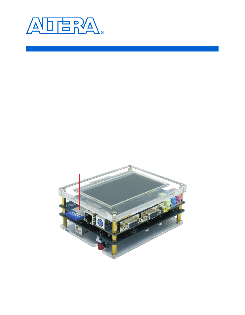
Figure 1–1. LCD Multimedia HSMC in Nios II Embedded Evaluation Kit
LCD Multimedia HSMC
Cyclone III FPGA Starter Board
The top view of the LCD Multimedia HSMC is shown in Figure 1–2.
Altera Corporation 1–1
August 2008 Preliminary
Page 5
There are several sample software applications that highlight the LCD
Touchpanel, SD-Card, and Ethernet components of the LCD Multimedia
HSMC in the Nios II Development Kits.
f For more information, refer Nios II Embedded Evaluation kit Getting Started
User Guide as an example.
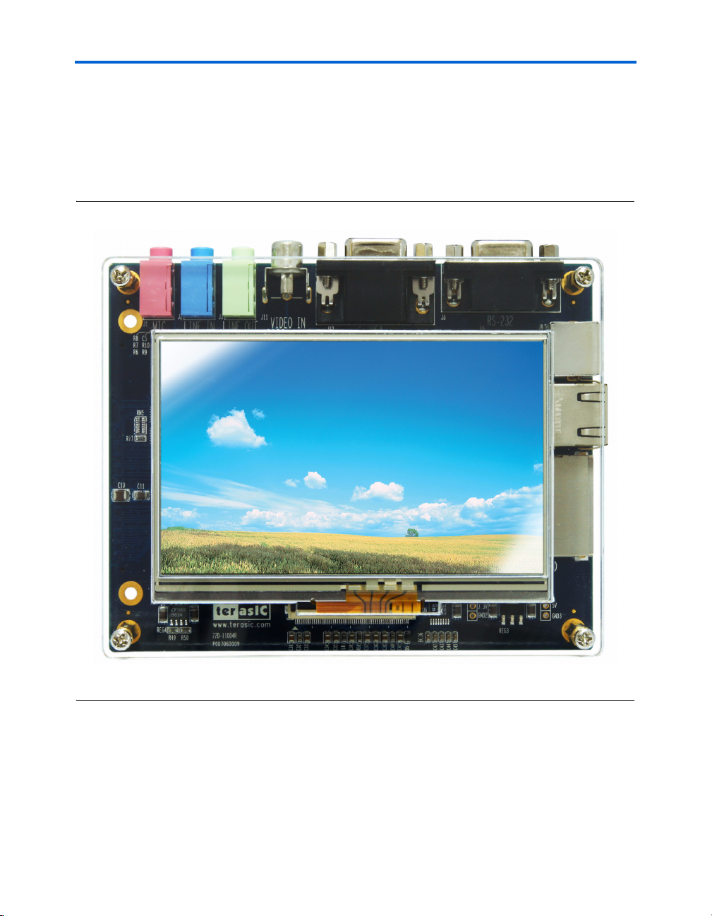
Figure 1–2. Top View of the LCD Multimedia HSMC
Connector view1 and connector view2 of the LCD Multimedia HSMC is
shown in Figure 1–3 and Figure 1–4.
1–2 Altera Corporation
LCD Multimedia HSMC August 2008
Page 6
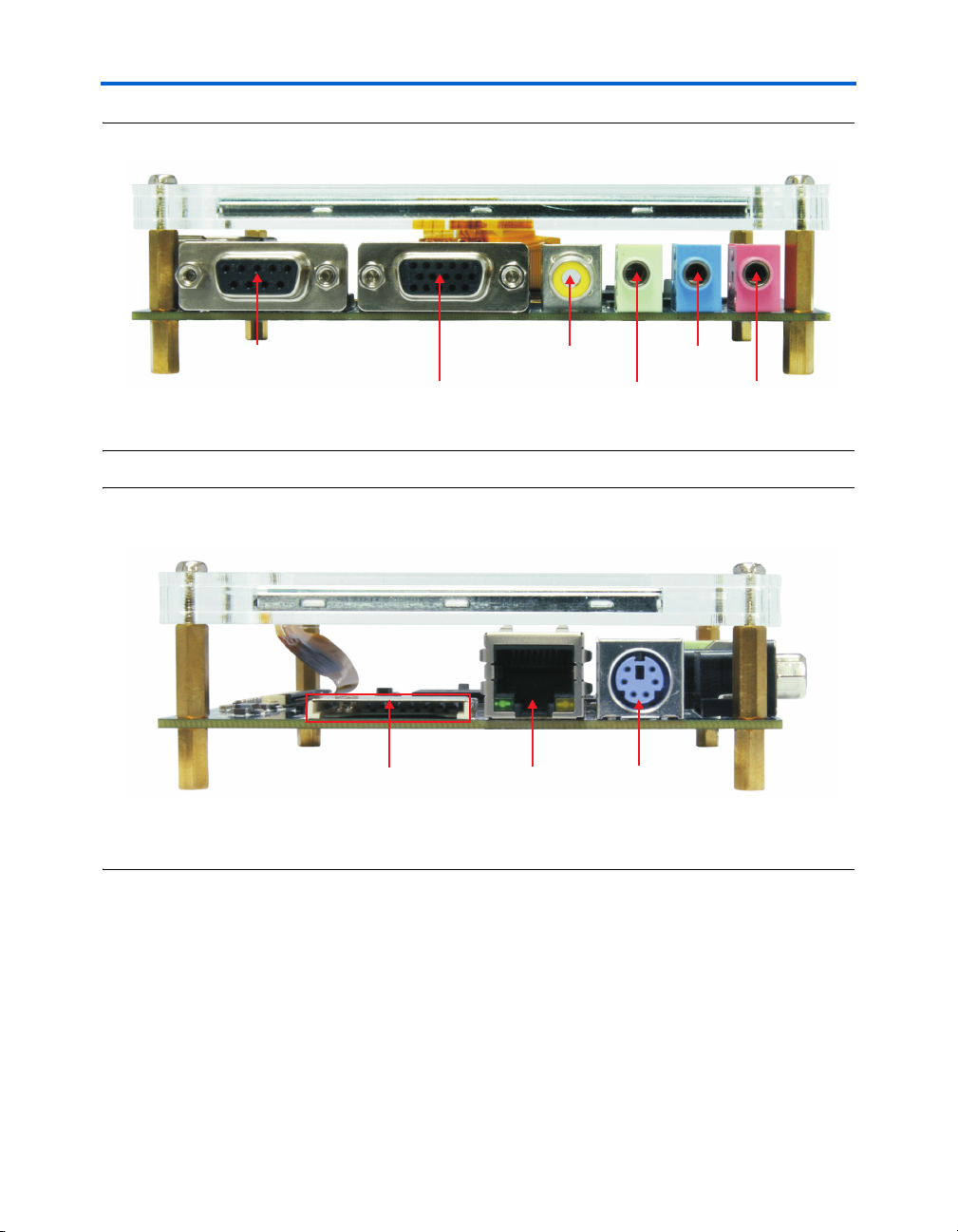
Figure 1–3. LCD Multimedia HSMC Side View 1
Overview
RS-232
VGA Out
Figure 1–4. LCD Multimedia HSMC Side View 2
SD-Card
Composite
Video In
Ethernet
RJ-45
Audio Out
PS/2
Audio In
Microphone In
Components and Block Diagram
The LCD Multimedia HSMC contains the following components.
■ MAX II CPLD EPM2210F324
● 2210 Logic elements
● 272 User I/Os
● 324 pin FineLine BGA package
■ LCD Touch-screen Display
● 800 X 480 pixel 4.3" Display
Altera Corporation 1–3
August 2008 LCD Multimedia HSMC
Page 7

■ 24-bit Audio Codec
■ SD Flash Connector
■ 10/100 Ethernet physical layer (PHY)
■ PS/2 Connector
■ Other Interfaces
● RS-232 Level-shifters
● RCA Jack (Video In)
● 10-bit VGA Output DAC
● Composite Video ADC
Block Diagram
Figure 1–5 shows a functional block diagram of the LCD Multimedia
HSMC.
1–4 Altera Corporation
LCD Multimedia HSMC August 2008
Page 8
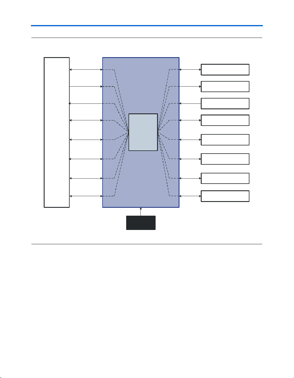
Figure 1–5. LCD Multimedia HSMC
HSMC
Connector
MAXII CPLD & Level Shift
BUS
Controller
Overview
24-bit AUDIO CODEC
VGA 10-bit Video DAC
Video decoder
PS2 & RS232 Ports
LCD Touch Panel
module
10/100 Ethernet PHY
SD Card
I2C EEPROM
100M Hz OSC
Altera Corporation 1–5
August 2008 LCD Multimedia HSMC
Page 9

2. Board Components and Interfaces
Board Overview
f For information on powering-up the LCD Multimedia HSMC and
This chapter provides operational and connectivity detail for the LCD
Multimedia HSMC's major components and interfaces and is divided
into the following major blocks:
■ MAX II CPLD used for
● Time-division multiplexing of signals
● Voltage level shifting
■ Interfaces
● HSMC expansion interface
● Audio codec interface
● Video decoder interface
● VGA interface
● Serial interface
● PS/2 interface
● Ethernet
■ Clocking circuitry
■ Memory
■ Power supply
1 Board schematics, board layout database, and assembly files for
the LCD Multimedia HSMC are included in the
board_design_files subdirectory of the installed kit directory.
installing the demo software and examples, refer to the user guide
provided with your kit.
Altera Corporation 2–1
August 2008 Preliminary
Page 10

Figure 2–1 shows the top view of the LCD Multimedia HSMC.
C
Figure 2–1. Top View of the LCD Multimedia HSMC
Board Components and Interfaces
RS-232 PortVGA Video PortVideo inLine OutLine inMic in
VGA 10-bit DA
24-bit Audio Codec
Video Decoder
(NTSC/PAL)
Altera MAX II 2210
CPLD device
100-MHz Oscillator
Notes:
(1) LCD Touch Panel is not shown.
LCD Touch Panel Connector
Ethernet 10/100M PHY
EEPROM
PS/2 Keyboard/
Mouse Port
Ethernet
10/100M Port
SD Card Slot
Altera Corporation 2–2
August 2008 LCD Multimedia HSMC
Page 11
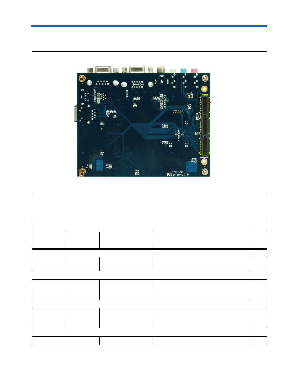
Figure 2–2 shows the back view of the LCD Multimedia HSMC.
Figure 2–2. Back View of the LCD Multimedia HSMC
Table 2–1 lists the components and their corresponding board references.
HSMC Connector
Table 2–1. LCD Multimedia HSMC (Part 1 of 2)
Typ e
Interface Device
CPLD MAX II U4 EPM2210F324C4, 272-pin FineLine BGA
Level Translator
I/O Bidirectional
Display
I/O LCD Touch
Connections & Interfaces
Input MIC In J1, U1 Microphone in jack 2–15
2–3 Altera Corporation
LCD Multimedia HSMC August 2008
Component/
Interface
Level Shift
Interface
Screen
Display
Board Reference Description Page
2–4
324-pin package
U10, U11 MAX 3378 Dual Low-Voltage Level
Translators
J10 +Touchscreen, U6 FPC 60B connector 2–10
2–8
Page 12
Table 2–1. LCD Multimedia HSMC (Part 2 of 2)
Board Components and Interfaces
Typ e
Input Line In J2, U1 24 bit CD quality audio CODEC 2–15
Output Line Out J3, U1 24 bit CD quality audio CODEC 2–15
Input SD Card
I/O Ethernet J5, U2 10/100 Ethernet PHY/MAC controller 2–19
I/O RS 232 J8, U5 9 pin connector and transceiver 2–21
I/O PS/2 J9 5 pin connector, mouse/ keyboard connector 2–22
Input Video
Output VGA J12, U9
Clock Circuitry
Oscillator Clock Y1, Y2, Y3 Various clock oscillators used for system
Powe r Supply
Powe r
Supplies
EEPROM
Memory I2C EEPROM U3 Uses one 2K bit EEPROM. 2–32
Expansion Interface
I/O HSMC J6 Expansion connector used to interface with
Component/
Interface
Socket
Decoder
Analog/Digital
Power
Board Reference Description Page
J4 128 MB Memory Card 2–17
J11 RCA jack 2–23
2–26
2–30
2–31
2–34
Reg1, Reg2, Reg3,
Reg4, Reg5
One VGA output connector (DB15)
10-bit VGA DAC
clock or other dedicated devices.
Switching and linear regulators used for
powering analog and digital components.
Altera starter and development boards
, and
Interface Device
MAX II CPLD-EPM2210F324 (U4)
The LCD Multimedia HSMC uses the MAX II 2210 CPLD
EPM2210F324C3 device (U4)
. Table 2–2 lists MAX II CPLD board
reference and manufacturing information.
Table 2–2. MAX II CPLD Manufacturing Information
Board Reference Device Description Manufacturer
U4 MAX II CPLD for TDM and
level shifting/buffering
Altera Corporation 2–4
August 2008 LCD Multimedia HSMC
Altera EPM2210F324C3N www.altera.com
Manufacturer Part
Number
Manufacturer
Website
Page 13
Interface Device
The primary functions for this device are to
1. Provide time-division multiplexing (TDM) functions to the LCD
and VGA color data bus.
2. Provide level shifting feature for the 2.5V input (Cyclone III FPGA)
and 3.3V required by many of the interface chips.
This package has 272 user I/Os and comes in a 324-pin Fine-Line BGA
package. Table 2–3 lists Max II device features.
Table 2–3. Max II Device Features
Architectural Feature Results
Altera’s second generation
low-cost CPLDs
Lowest power
consumption CPLD
On-chip user Flash memory ● 8kbit user accessible flash memory
● Low cost packaging
● Large number of logic elements
● LUT based architecture
● Fastest CPLD supports up to 300MHz clock frequency
● Power down capability that conserves the battery life
● Lowest dynamic power
● Hot-socketing support
● Single power supply simplicity
● Enables the integration of discrete and non-volatile storage
reducing chip count and cost
Real time In-signal
programmability
I/O capabilities
● Capable of downloading a second design while the device is
operational
● Supports interfacing with 1.8V, 2.5V and 3.3V logic levels of the
device due to Multivolt I/O capability
● Schmitt triggers, programmable slew rate & programmable drive
strength improve signal integrity
2–5 Altera Corporation
LCD Multimedia HSMC August 2008
Page 14
Board Components and Interfaces
Table 2–4 lists the Max II EPM2210F324C4 device pin count.
Table 2–4. Max II Device Pin Count
Board Component Pins
SD Card 6
Ethernet 18
Audio Codec 6
RS232 and PS/2 4
LCD Touch Panel 38
Video Decoder 14
VGA 25
MAX II CPLD ISP 4
HSMC(1) 88
Total Pins Used 203
Total EPM2210F324C4 User I/Os 272
Unused pins 69
Note to Ta b l e 2– 4 :
(1) The HSMC pins include all pins between the FPGA and the MAX II CPLD
f For additional information about Altera devices, go to
www.altera.com/products/devices.
Block Diagram of bus-controller logic in the MAX II CPLD
Figures 2–3 shows the block diagram of Bus Controller logic in the MAX
II device. Both the LCD TDM block is a simple 8-bit to 24-bit data
de-multiplexing function which drives the LCD panel. Similarly, the
VGA TDM block is a 10bit to 30bit data de-multiplexing function which
drives the VGA DAC. In the LCD TDM block, the 8-bit input data
(successive BGR color data) comes in at 3x the rate of the 24-bit output
data bus (8-bit B + 8bit G + 8bit R).
1 The purpose of adding this complexity to the design of the LCD
Multimedia HSMC was to allow for more functionality given
the constraint of a pin-limited HSMC connector interface.
The I2CBir_bus block provides birdirectional control for I2C Serial
EEPROM data bus. All other signals that pass through the MAXII device
are uni-directional and are simply buffered and level-shifted in the
MAX II.
Altera Corporation 2–6
August 2008 LCD Multimedia HSMC
Page 15
Interface Device
Figure 2–3. The Block Diagram of MAX II Bus Controller
LCD Touch Panel &
AD co nverter
Serial Port Int erface
LCD Col or Dat a B us (RGB )
LCD Timin g Con trol Bu s
MAXII CPLD
LCD TDM
Controller
LCD R dat a
LCD G data
LCD B data
LCD Timi ng Cont rol Bu s
LCD Touch Panel Module
HSMC
Connector
VGA Color Dat a Bus (RGB )
VGA Timing Cont rol Bu s
I2C EE PROM Interf ace
Bi-directional I /Os
The source code for this design in the MAXII device can be found in the
"board_design_files" directory for your development kit.
VGA R dat a
VGA TDM
Controller
I2C_bir_bus
Controller
Other uni -directi onal I /Os
Bi-directional Level
VGA G data
VGA B dat a
VGA Timing Control Bus
Translator
VGA
DAC
I2C E EPROM
AUDIO DAC
Ethernet PHY
SD Card
RS232 Ports
Video Decod er
2–7 Altera Corporation
LCD Multimedia HSMC August 2008
Page 16
Board Components and Interfaces
Level Translator
Bidirectional level shift interface
The board provides bidirectional level shift feature for the 2.5V input
(Cyclone III FPGA) and 3.3V required by many of the interface chips via
two Maxim MAX3378 level translators. Tab l e 2– 5 lists bidirectional level
shift interface reference and manufacturing information.
Table 2–5. Bidirectional Level Shift Interface Manufacturing Information
Board Reference Device Description Manufacturer
U10, U11 Dual Low-Voltage
Level Translators
Maxim Integrated
Products
Manufacturer Part
MAX3378EEUD www.maxim-ic.com
Figure 2–4 shows the block diagram and pinout of the bidirectional level
shift interface on the board respectively.
Figure 2–4. Block Diagram of Bidirectional Level Shift Interface
HC_I2C_SDAT
HC_PS2_CLK
HC_PS2_DAT
Level
Translator
(U10)
I2C_SDAT
PS2_CLK
PS2_DA T
Number
Manufacturer
Website
Video
Decoder
& Audio
DAC
PS/2
Port
HC_MDIO
MDIO
Eth ern et
PHY
HSMC
Connector
HC_SD_DAT3
HC_SD_CMD
HC_SD_DAT
Level
Translator
SD_DAT3
SD_CMD
SD_DAT
SD Card
Socket
(U11)
LCD
HC_SDA
SDA
Touch
Panel
Module
Altera Corporation 2–8
August 2008 LCD Multimedia HSMC
Page 17

Level Translator
Table 2–6 shows the pinouts of Level Shift Inteface with HSMC connector.
Table 2–6. Level Shift Interface Pinouts with HSMC Connector
HSMC Side Signal
Name
HC_I2C_SDAT 33 I2C_SDAT U1-27;U8-33 Audio CODEC ADC LR Clock
HC_PS2_CLK 43 PS2_CLK J9-6 PS/2 Clock
HC_PS2_DAT 47 PS2_DAT J9-1 PS/2 Data
HC_MDIO 49 MDIO U2-30 Ethernet PHY Management Data I/O
HC_SD_DAT3 53 SD_DAT3 J4-1 SD 1-bit Mode: Card Detect; SPI Mode:
HC_SD_CMD 44 SD_CMD J4-2 SD 1-bit Mode: Command Line; SPI
HC_SD_DAT 48 SD_DAT J4-7 SD 1-bit Mode: Data Line; SPI Mode:
HC_SDA 50 SDA J10-44 LCD 3-Wire Serial Interface Data
HSMC Pin
No.
Device Side
Signal
Level Shift
Interface Pin No.
Level Shift Interface Description
Chip Select (Active Low)
Mode: Data In
Data Out
Figure 2–5 shows the Level Shift Interface schmeatic.
Figure 2–5. Level Shift Interface Schematic
2–9 Altera Corporation
LCD Multimedia HSMC August 2008
Page 18

Board Components and Interfaces
Display
LCD Touch Panel Display
The board provides a 4.3" Toppoly TD043MTEA1 active matrix color
display, with 800x480 pixel resolution. Ta bl e 2– 7 lists LCD Touch Panel
Display board reference and manufacturing information.
Table 2–7. LCD Touch Panel Display Manufacturing Information
Board Reference Device Description Manufacturer
Display + J10 4.3" Active Matrix
Color LCD Screen
(480x800 RGB) +
Touch Panel
U6 12-Bit ADC for
resistive
touchscreen sensing
Toppoly TD043MTEA1 www.toppoly.com
Analog Devices AD7843 www.analog.com
The LCD panel supports the 24-bit parallel RGB data interface and
provides a 3-wire interface to control the display function registers. The
LCD Multimedia HSMC is also equipped with an Analog Devices
AD7843 touch screen digitizer chip. The AD7843 is a 12-bit analog to
digital converter (ADC) for digitizing x and y coordinates of touch points
applied to the touch screen.
Manufacturer Part
Number
Manufacturer
Website
Timing Protocol of the LCD TDM Controller
Figure 2–6 below describes the input timing waveform information of the
LCD TDM Controller implemented in the MAX II CPLD. The 8-bit wide
HC_LCD_DATA signal is presumed to contain a stream of color pixel
data, with each pixel represented by three successive clock-cycles of the
stream. The data is presented in the order "BGR". The LCD TDM
Controller uses the HC_HD pulse to determine the position of the BLUE
color sample, and thus the start of each three-clock pixel-period. State
transitions on HC_HD (0.1 or 1.0) coincide with the presentation of
BLUE color on the HC_LCD_DATA input. The GREEN and RED values
for that same pixel are presented on the next two clock-cycles. Figure 2–7
shows the timing information on the output side. The LCD TDM block
will generate an output NCLK clock and 24-bit RGB data to the LCD
panel. The NCLK signal runs at 1/3 the frequency of the incoming clock
HC_NCLK.
Altera Corporation 2–10
August 2008 LCD Multimedia HSMC
Page 19

Display
Figure 2–6. The Timing Diagram On the Input Side of VGA TDM Controller
HC_NCLK
HC_LCD_DATA
B G R B G R
HC_HD
Figure 2–7. The Timing Diagram On the Output Side of VGA TDM Controller
HC_NCLK
LCD R, G , B
Color data
HD, VD, DEN
Sync Signals
NCLK
{ R:G:B } { R:G:B }
HD, VD, DEN
HD, VD, DEN
The pin assignments are listed in Tables 2–8
Tables 2–8 shows the pinout of LCD Touch Panel with HSMC connector.
Table 2–8. LCD Touch Panel Pinout with HSMC Connector
HSMC Connector MAX II LCD Touch Panel
HSMC
Signal Name
HC_VD
HC_HD
2–11 Altera Corporation
LCD Multimedia HSMC August 2008
Pin
Connector
No.
Side Pin
132 D14 F6
134 C14 F5
Device
Side Pin
Signal Name Pin No. Description
VD
HD
6 LCD Vertical Sync Input
7 LCD Horizontal Sync Input
Page 20

Table 2–8. LCD Touch Panel Pinout with HSMC Connector
HSMC Connector MAX II LCD Touch Panel
HSMC
Signal Name
HC_DEN
HC_NCLK
HC_LCD_DATA[0]
HC_LCD_DATA[1]
HC_LCD_DATA[2]
HC_LCD_DATA[3]
HC_LCD_DATA[4]
HC_LCD_DATA[5]
HC_LCD_DATA[6]
HC_LCD_DATA[7]
HC_GREST
HC_SCEN
Pin
Connector
No.
Side Pin
138 C15 E5
95 K13 E4
145 D17 H1
149 C17 H2
151 C16 J2
126 D13 J1
128 D15 J3
146 B15 K3
150 B14 K1
152 A15 K2
140 C13 L2
144 B13 L1
Device
Side Pin
E3
D4
F3
C3
F1
C2
F2
D3
G2
D1
G1
D2
G3
E2
H3
E1
Signal Name Pin No. Description
DEN
NCLK
R[0]
G[0]
B[0]
R[1]
G[1]
B[1]
R[2]
G[2]
B[2]
R[3]
G[3]
B[3]
R[4]
G[4]
B[4]
R[5]
G[5]
B[5]
R[6]
G[6]
B[6]
R[7]
G[7]
B[7]
GREST
SCEN
Board Components and Interfaces
8 LCD RGB Data Enable
9LCD Clock
28 LCD red data bus bit 0
19 LCD green data bus bit 0
10 LCD blue data bus bit 0
29 LCD red data bus bit 1
20 LCD green data bus bit 1
11 LCD blue data bus bit 1
30 LCD red data bus bit 2
21 LCD green data bus bit 2
12 LCD blue data bus bit 2
31 LCD red data bus bit 3
22 LCD green data bus bit 3
13 LCD blue data bus bit 3
32 LCD red data bus bit 4
23 LCD green data bus bit 4
14 LCD blue data bus bit 4
33 LCD red data bus bit 5
24 LCD green data bus bit 5
15 LCD blue data bus bit 5
34 LCD red data bus bit 6
25 LCD green data bus bit 6
16 LCD blue data bus bit 6
35 LCD red data bus bit 7
26 LCD green data bus bit 7
17 LCD blue data bus bit 7
40 LCD Global Reset, Low
Active
42 LCD 3-Wire Serial
Interface Enable
Altera Corporation 2–12
August 2008 LCD Multimedia HSMC
Page 21

Display
Table 2–8. LCD Touch Panel Pinout with HSMC Connector
HSMC Connector MAX II LCD Touch Panel
HSMC
Signal Name
HC_SDA
HC_ADC_DCLK
HC_ADC_DIN
HC_ADC_CS_n
HC_ADC_DOUT
HC_ADC_PENIRQ_n
HC_ADC_BUSY
Notes to Ta b l e 2– 8 :
(1) These signals do not go through the MAX II chip. They pass through the MAX3378 level translator chip, U11.
Pin
Connector
No.
Side Pin
50
U11-5
157 B18 L3
155 B16 N2
143 D18 N1
122 E13 M1
156 A14 M3
120 E15 M2
(1)
Device
Side Pin
U11-10(1
Signal Name Pin No. Description
)
SDA
ADC_DCLK
ADC_DIN
ADC_CS_n
ADC_DOUT
ADC_PENIRQ_n
ADC_BUSY
J10.44 LCD 3-Wire Serial
Interface Data
U6.16 AD7843/LCD 3-Wire Serial
Interface Clock
U6.14 AD7843 Serial Interface
Data In
U6.15 AD7843 Serial Interface
Chip Select Input
U6.12 AD7843 Serial Interface
Data Out
U6.11 AD7843 pen Interrupt
U6.13 AD7843 Serial Interface
Busy
Figure 2–8 shows the LCD Touch Panel schematic.
2–13 Altera Corporation
LCD Multimedia HSMC August 2008
Page 22

Figure 2–8. LCD Touch Panel Schematic
R
R
R[0.. 7]
G[0..7]
B[0..7 ]
VCC33
R58 10KR58 10K
R59 10KR59 10K
R60 10KR60 10K
R61 10KR61 10K
R62 10KR62 10K
X_RIGHT
X_LEFT
Y_TOP
Y_BOTTOM
X_RIGHT
Y_TOP
X_LEFT
Y_BOTTOM
VCC33
10
HVDE
SDA
ADC_PENIRQ_n
ADC_CS_n
SCEN
C42 10NC42 10N
C43 10NC43 10N
C44 10NC44 10N
C45 10NC45 10N
1
2
4
3
5
7
8
6
U6
+VCC
+VCC
X+
X-
Y+
Y-
IN3
IN4
GND
AD7843U6AD7843
16
DCLK
15
CS
14
DIN
13
BUSY
12
DOUT
11
PENIRQ
9
VREF
VCC33
VCC33
VDDN
D5 PMEG2010ABED5 PMEG2010ABE
ADC_DCLK
ADC_CS_n
ADC_DIN
ADC_BUSY
ADC_DOUT
ADC_PENIRQ_n
R57 33R57 33
U7
U7
V+
V+
1
TRIM
TRIM
2
V-
V-
ADR525
ADR525
C31 2.2UC31 2.2U
CGH
C33 2.2UC33 2.2U
VCOM
C34 2.2UC34 2.2U
C35 2.2UC35 2.2U
VDDP
C36 2.2UC36 2.2U
VDDN
C37 2.2UC37 2.2U
C38 2.2UC38 2.2U
VMP
C39 2.2UC39 2.2U
VMN
C41 2.2UC41 2.2U
CGL
3
VCC33
Board Components and Interfaces
J10
J10
1
1
2
2
3
3
4
4
5
5
6
6
7
7
8
8
9
9
10
10
11
11
12
12
13
13
14
14
15
15
16
16
17
17
18
18
19
19
20
20
21
21
22
22
23
23
24
24
25
25
26
26
27
27
28
28
29
29
30
30
31
31
32
32
33
33
34
34
35
35
36
36
37
37
38
38
39
39
40
40
41
41
42
42
43
43
44
44
45
45
46
46
47
47
48
48
49
49
50
50
51
51
52
52
53
53
54
54
55
55
56
56
57
57
58
58
59
59
60
60
616162
FPC-60B_CONNECTO
FPC-60B_CONNECTO
GND
VCC
VDDP
VDDN
SCL
VCC
GND
LED B+
LED B-
62
VCC33
+5V
LED_B+
LED_B-
CGH
CPL1
CPL2
VCOM
VD
HD
DEN
NCLK
B0
B1
B2
B3
B4
B5
B6
B7
G0
G1
G2
G3
G4
G5
G6
G7
R0
R1
R2
R3
R4
R5
R6
R7
VDDP
TP_AGND
VDDN
-5V
HVDE
GREST
STBY
SCEN
ADC_DCLK
SDA
FB
VMP
VMN
C11
C12
CGL
Y_TOP
X_LEFT
Y_BOTTOM
X_RIGHT
Altera Corporation 2–14
August 2008 LCD Multimedia HSMC
Page 23

Interfaces/ Connectors
Interfaces/
This section describes the following LCD Multimedia HSMC’s
interface/connector blocks:
Connectors
■ Audio Codec Interface (J1, J2, J3)
■ SD Card socket (J4)
■ Ethernet connector (J5)
■ RS 232 connector (J8)
■ UART and PS/2 connector (J9)
■ Video Decoder connector (J11)
■ VGA DAC connector (J12)
Audio Codec Interface
The board provides 24-bit CD-Quality audio via the Wolfson WM8731
audio CODEC (enCODer/DECoder). Table 2–9 lists Audio Codec
Interface board reference and manufacturing information.
Table 2–9. Audio Codec Interface Manufacturing Information
Board Reference Device Description Manufacturer
U1 CD quality, low power,
high quality audio codec.
The Audio Codec Interface features:
Wolfson
Microelectronics
Manufacturer Part
Number
WM8731 www.wolfsonmicro.com
Manufacturer Website
■ 24-bit sigma-delta audio CODEC
■ Line-level input, line-level output, and microphone input jacks
■ Sampling frequency: 8 to 96 KHz
This chip supports microphone-in (J1), audio-in (J2), and audio-out (J3)
ports, with a sample rate adjustable from 8 kHz to 96 kHz. The WM8731
is controlled by a serial I2C bus interface, which is connected to pins on
the HSMC connector.
2–15 Altera Corporation
LCD Multimedia HSMC August 2008
Page 24

Board Components and Interfaces
Tables 2–10 shows the pinout of Audio Codec with HSMC connector.
Table 2–10. Audio Codec Pinout with HSMC Connector
HSMC Connector MAX II Audio Codec
HSMC
Signal Name
HC_AUD_BCLK
HC_AUD_XCK
HC_AUD_DACDAT
HC_AUD_DACLRCK
HC_AUD_ADCDAT
HC_AUD_ADCLRCK
HC_I2C_SDAT
HC_I2C_SCLK
Note:
(1) These signals do not go through the MAX II chip. They pass through the MAX3378 level translator chip, U10.
(2) Default, the audio chip is configured as a SLAVE mode.
Pin
No.
113
39
109
107
40
103
33
34
Connector
Side Pin
G17
T16
H17
H18
R15
H16
U10-2
P15
(1)
Device
Side Pin
U13
U14
V13
T13
T12
V12
U10-13(1
U11
Signal Name
AUD_BCLK
AUD_XCK
AUD_DACDAT
AUD_DACLRCK
AUD_ADCDAT
AUD_ADCLRCK
)
I2C_SDAT
I2C_SCLK
Pin
No.
7 Audio CODEC Bit-Stream
Clock
1 Audio CODEC Chip Clock
8 Audio CODEC DAC Data
9 Audio CODEC DAC LR Clock
10 Audio CODEC ADC Data
11 Audio CODEC ADC LR Clock
27 I2C Data
28 I2C Clock
Description
Altera Corporation 2–16
August 2008 LCD Multimedia HSMC
Page 25

Interfaces/ Connectors
Figure 2–9 shows the Audio Codec connector schematic.
Figure 2–9. Audio Codec Connector Schematic
C1 1UC1 1U
VCC33VCC33
R52KR5
R42KR4
2K
I2C_SDAT
I2C_SCLK
AUD_XCK
AUD_BCLK
AUD_DACDAT
AUD_DACLRCK
AUD_ADCDAT
AUD_ADCLRCK
2K
VCC33
1
2
3
4
5
6
7
U1
AGND
XTI/MCLK
XTO
DCVDD
DGND
DBVDD
CLKOUT
BCLK
22
28
24
25
27
23
26
CSB
SDIN
SCLK
MICIN
MODE
LLINEIN
RLINEIN
21
MBIAS
20
VMID
19
ADCLRCK11ADCDAT
10
A_VCC33
AGND
18
AVDD
17
ROUT
16
LOUT
15
HPGND
HPVDD
RHPOUT14LHPOUT
12
13
TC1 100U/6.3VTC1 100U/6.3V
WM8731U1WM8731
DACDAT8DACLRCK9EXPOSED
29
C2 1UC2 1U
C4 10UC4 10U
A_VCC33
AGND
TC2 100U/6.3VTC2 100U/6.3V
AGND
R6 330R6 330
R7 680R7 680
AGND
R2
4.7KR24.7K
C51NC5
1N
R9
47KR947K
R0 4.7KR0 4.7K
R1 4.7KR1 4.7K
R3
4.7KR34.7K
AGND
C31UC3
1U
R8
47KR847K
AGNDAGND
R10
R10
47K
47K
J2
J2
J1
J1
J3
J3
LINE IN
5
MIC IN
5
LINE OUT
5
L1R2GND3NCR4NCL
PHONE JACK B
PHONE JACK B
AGND
L1R2GND3NCR4NCL
PHONE JACK P
PHONE JACK P
AGND
L1R2GND3NCR4NCL
PHONE JACK G
PHONE JACK G
AGND
AGND AGND
SD Card
The board includes a SD Card socket and provides SPI mode for SD Card
access. It can be accessible as memory in both SPI and and 1-bit SD mode.
The SD-Card data, clock, and control signals are wired directly to the
MAX II CPLD.
2–17 Altera Corporation
LCD Multimedia HSMC August 2008
Page 26

Board Components and Interfaces
Tables 2–11 shows the pinout of SD Card Socket with HSMC connector.
Table 2–11. SD Card Pinout with HSMC Connector
HSMC Connector MAX II SD Card
HSMC
Signal Name
HC_SD_DAT3
Pin
No.
53
Connector
Side Pin
U11-2
(1)
Device
Side Pin
U11-13(1
Signal Name
)
SD_DAT3
Pin
No.
Description
1 SD 1-bit Mode: Card Detect;
SPI Mode: Chip Select
(Active Low)
HC_SD_CMD
44
U11-3
(1)
U11-12(1
)
SD_CMD
2 SD 1-bit Mode: Command
Line; SPI Mode: Data In
HC_SD_CLK
HC_SD_DAT
101 J16 P1
U11-4
(1)
U11-11(1
48
)
SD_CLK
SD_DAT
5Clock
7 SD 1-bit Mode: Data Line;
SPI Mode: Data Out
Notes:
(1) These signals do not go through the MAX II chip. They pass through the MAX3378 level translator chip, U11.
Figure 2–10 shows the SD Card interface schematic.
Figure 2–10. SD Card Interface Schematic
VCC33 VCC33
R38
R38
4.7K
4.7K
SD_DAT3
SD_CMD
SD_CLK
SD_DAT
Altera Corporation 2–18
August 2008 LCD Multimedia HSMC
R39
R39
4.7K
4.7K
VCC33
R42
R42
4.7K
4.7K
VCC33
J4
J4
DAT2
DAT2
9
DAT3
DAT3
1
CMD
CMD
2
VSS
VSS
3
VCC
VCC
4
CLK
CLK
5
VSS
VSS
6
DAT0
DAT0
7
DAT1
DAT1
8
SW0
SW0
10
SW1
SW1
11
SD Card Socket
121314
SD Card Socket
15
Page 27

Interfaces/ Connectors
Ethernet PHY
Ethernet support is provided via the National Semiconductor DP83848C
Ethernet Physical Layer Transceiver chip and an RJ-45 connector (J5).
Table 2–12 lists Ethernet PHY board reference and manufacturing
information.
Table 2–12. Ethernet PHY Manufacturing Information
Board Reference Device Description Manufacturer
U2 Single Port 10/100
Mb/s Ethernet
Physical Layer
Transceiver
National
Semiconductor
The DP83848C device has the following features:
■ Single Port 10/100 Mb/s Ethernet Physical Layer Transceiver
■ Supports both 100Base-T and 10Base-T Ethernet protocols
■ Supports Auto-MDIX for 10/100 Mb/s
The DP83848C is one port Fast Ethernet PHY Transceivers supporting
IEEE 802.3 physical layer applications at 10 Mbps and 100 Mbps. The
DP83848C provides Media Independent Interface (MII) to connect
DP83848C to a MAC in the FPGA.
Tables 2–13 shows the pinout of Ethernet PHY with HSMC connector.
Table 2–13. Ethernet PHY Pinout with HSMC Connector
HSMC Connector MAX II Ethernet PHY
HSMC
Signal Name
HC_TX_CLK
HC_TX_EN
HC_TXD[0]
HC_TXD[1]
HC_TXD[2]
HC_TXD[3]
HC_ETH_RESET_N
Pin
Connector
No.
Side Pin
158 A13 T2
125 F18 R3
127 F17 P4
131 E17 R1
133 E18 R2
137 E16 P2
121 F16 T3
Device
Side Pin
Signal Name
TX_CLK
TX_EN
TXD0
TXD1
TXD2
TXD3
Eth_RESET_N
Manufacturer Part
Number
DP83848C www.national.com
Pin
No.
1 MII Transmit Clock
2 MII Transmit Enable
3 MII Transmit Data bit 0
4 MII Transmit Data bit 1
5 MII Transmit Data bit 2
6 MII Transmit Data bit 3
29 DP83848C Reset
Manufacturer
Website
Description
2–19 Altera Corporation
LCD Multimedia HSMC August 2008
Page 28

Board Components and Interfaces
Table 2–13. Ethernet PHY Pinout with HSMC Connector
HSMC Connector MAX II Ethernet PHY
HSMC
Signal Name
HC_MDIO
HC_MDC
HC_RX_CLK
HC_RX_DV
HC_RX_CRS
HC_RX_ERR
HC_RX_COL
HC_RXD[0]
HC_RXD[1]
HC_RXD[2]
HC_RXD[3]
Notes:
(1) These signals do not go through the MAX II chip. They pass through the MAX3378 level translator chip, U10.
Pin
Connector
No.
Side Pin
49
U10-5
139 D16 U1
96 H14 J5
116 E14 H5
92 H15 H4
90 G13 H6
114 F14 G6
102 G15 G4
104 G12 G5
108 F13 G7
110 F15 F4
(1)
Device
Side Pin
U10-10(1
Signal Name
)
MDIO
MDC
RX_CLK
RX_DV
RX_CRS
RX_ERR
RX_COL
RXD0
RXD1
RXD2
RXD3
Pin
No.
30 Management Data I/O
31 Management Data Clock
38 MII Receive Clock
39 MII Receive Data valid
40 MII Carrier Sense
41 MII Receive Error
42 MII Collision Detect
43 MII Receive Data bit 0
44 MII Receive Data bit 1
45 MII Receive Data bit 2
46 MII Receive Data bit 3
Description
Figure 2–11 shows the Ethernet PHY connector schematic.
Altera Corporation 2–20
August 2008 LCD Multimedia HSMC
Page 29

Interfaces/ Connectors
Figure 2–11. Ethernet PHY Schematic
VCC33
VCC33
TXD[0..3]
RXD[0..3 ]
RX_CLK
RX_DV
RX_CRS
RX_ERR
RX_COL
RXD0
RXD1
RXD2
RXD3
R15 33R15 33
R16 33R16 33
R17 33R17 33
R18 33R18 33
R19 33R19 33
R20 33R20 33
R21 33R21 33
R22 33R22 33
R23 33R23 33
BC5
BC5
Y1
4
1
VCC
EN
0.1U
0.1U
2
OUT3GND
VCC33
25MHZY125MHZ
C6
10UC610U
PFBOUT
BC7
BC7
0.1U
0.1U
E_AGND
37
38
39
40
41
42
43
44
45
46
47
VCC33
48
BC11
BC11
C9
0.1U
0.1U
10UC910U
TX_CLK
TX_EN
TXD0
TXD1
TXD2
TXD3
BC6
BC6
0.1U
0.1U
35
36
U2
DGND
PFBIN2
RX_CLK
RX_DV/MII _MODE
CRS/CRS_DV/L ED_CFG
RX_ER/MDIX_EN
COL/PHYAD0
RXD_0/PHYAD1
RXD_1/PHYAD2
RXD_2/PHYAD3
RXD_3/PHYAD4
IOGND
IOVDD33
TX_CLK1TX_EN2TXD_03TXD_14TXD_25TXD_3/SNI_MODE6PWR_DOWN/INT7TCK8TDO9TMS10TRST#11TDI
R31 33R31 33
R32 33R32 33
R33 33R33 33
R34 33R34 33
R35 33R35 33
R36 33R36 33
MDIO
MDC
32
31
34
X233X1
MDC
IOGND
IOVDD33
DP83848CU2DP83848C
VCC33
R11
R11
1.5K
1.5K
ETH_RESET_N
R12 120R12 120
R13 120R13 120
R14 1KR14 1K
RBIAS
PFBOUT
AVDD33
AGND
PFBIN1
TD+
TD-
AGND
RD+
RD-
ACTIVITY
SPEED
PFBOUT
24
23
22
21
20
19
18
17
16
15
14
13
E_AGND
DUPLEXLEDR DUPLEXLEDR
R24 4. 7KR24 4. 7K
BC10 0.1UBC10 0.1U
R27
R27
49.9
49.9
E_AGND
ACTIVITY
100Mbps
DUPLEX
VCC33
C7
10UC710U
E_AGND
E_AGND
R28
R28
R29
R29
49.9
49.9
49.9
49.9
BC12
BC12
0.1U
0.1U
E_AGND
E_AVCC33
BC9
R25 2.2KR25 2.2K
R26 2.2KR26 2.2K
TD+
TD-
RD+
RD-
C8
10UC810U
E_AGND
E_AVCC33
BC14
BC14
0.1U
0.1U
E_AGND
BC9
0.1U
0.1U
E_AVCC33
BC15
BC15
0.1U
0.1U
E_AVCC33
E_AGND
16
J5
J5
1
TD+
MNT115MNT0
2
TD-
4
CTT
5
CTR
3
RD+
6
RD-
7
NC
8
CHSG
SMNT013SMNT1
14
YELLOW
YELLOW
GREEN
GREEN
RJ45INTLED
RJ45INTLED
ACTIVITY
11
D3
12
D4
SPEED
10
D2
9
D1
VCC33
BC8
BC8
0.1U
0.1U
R30
R30
49.9
49.9
E_AVCC33
BC13
BC13
0.1U
0.1U
ACT
SPE
DUPLEX
26
27
30
25
28
29
MDIO
RESET_N
25MHz_OUT
LED_LINK/AN0
LED_SPEED/AN1
RESERVED
LED_ACT/COL/AN_EN
RESERVED
12
R37
R37
2.2K
2.2K
RS232 Serial Interface
The board uses the ADM3202 transceiver chip and a 9-pin D-SUB
connector for RS-232 communications. Table 2–14 below lists RS 232
Serial Interface board reference and manufacturing information.
Table 2–14. RS232 Serial Interface Manufacturing Information
Board
Reference
U5 High-Speed, 2-Channel
Device Description Manufacturer
Analog Devices ADM3202 www.analog.com
RS232/V.28 Interface Devices
2–21 Altera Corporation
LCD Multimedia HSMC August 2008
Manufacturer Part
Number
Manufacturer
Website
Page 30

Tables 2–15 shows the pinout of RS232 Interface with HSMC connector.
Table 2–15. RS232 Interface Pinout with HSMC Connector
HSMC Connector MAX II RS232 Interface
HSMC
Signal Name
HC_UART_RXD
HC_UART_TXD
Pin
Connector
No.
Side Pin
115 G18 K4
119 G16 J4
Device
Side Pin
Signal Name Pin No. Description
UART_RXD
UART_TXD
Notes:
(1) U5.12 connects to pin 3 on the RS-232 connector (J6) via U5.13.
(2) U5.11 connects to pin 2 on the RS-232 connector (J6) via U5.14.
Figure 2–12 shows the RS232 interface schematic.
Figure 2–12. RS232 Interface Schematic
VCC33
RXD L EDRRXD L EDR
TXD LEDGTXD LEDG
R75 330R75 330
R76 330R76 330
UART_RXD
UART_TXD
C27 1UC27 1U
C28 1UC28 1U
UART_RXD
UART_TXD
12
9
11
10
1
3
4
5
2
6
C301UC30
C291UC29
1U
1U
U5
R1OUT
R2OUT
T1IN
T2IN
C+
C1C2+
C2V+
V-
Board Components and Interfaces
)
)
13
8
14
7
16
VCC33
15
UART Receiver
UART Transmitter
J8
5
9
4
8
3
7
2
6
1
ADM3202U5ADM3202
U5-12(1
U5-11(2
R1IN
R2IN
T1OUT
T2OUT
VCC
GND
RS232J8RS232
11
10
PS/2 Interface
The LCD Multimedia HSMC includes a standard PS/2 interface and a
connector (J9) for a PS/2 keyboard or mouse. The PS/2 interface is a
standard interface that is described extensively elsewhere.
Implementation of a PS/2 interface can be done ei ther in hardwa re on the
MAXII or FPGA or software in a Nios processor running on the FPGA.
Altera Corporation 2–22
August 2008 LCD Multimedia HSMC
Page 31

Interfaces/ Connectors
Tables 2–16 shows the pinout of PS/2 Interface with HSMC connector.
Table 2–16. PS/2 Interface Pinout with HSMC Connector
HSMC Connector MAX II PS/2 Interface
HSMC
Signal Name
HC_PS2_CLK
HC_PS2_DAT
Pin
No.
43
47
Connector
Side Pin
U10-3
U10-4
(1)
(1)
Device
Side Pin
U10-12(1
U10-11(1
Signal Name
)
PS2_CLK
)
PS2_DAT
Pin
No.
Description
1 PS/2 Clock
6 PS/2 Data
Notes:
(1) These signals do not go through the MAX II chip. They pass through the MAX3378 level translator chip, U10.
Figure 2–13 shows the PS/2 interface schematic.
Figure 2–13. PS/2 Interface Schematic
VCC5 VCC5
R532KR53
PS2_CLK
R542KR54
2K
2K
R56 120R56 120
R55 120R55 120
3
1
2
D3
BAT54SD3BAT54S
3
D4
BAT54SD4BAT54S
1
2
VCC33VCC33
VCC5
BC34
BC34
0.1U
0.1U
PS2DATPS2_DAT
PS2CLK
J9
J9
TOP
TOP
1
2
8 6
8 6
3
5
6
8
3
5
3
5
2 1
2 1
PS2
PS2
9
10
11
Video Decoder Interface
The board is equipped with an Analog Devices ADV7180 Video decoder
chip and RCA input jack (J11). Table 2–17 below lists Video Decoder
Interface board reference and manufacturing information.
Table 2–17. Video Decoder Interface
Board Reference Device Description Manufacturer
U8 10-Bit, 4× Oversampling
Analog Devices ADV7180 www.analog.com
Manufacturer Part
Number
SDTV Video Decoder
2–23 Altera Corporation
LCD Multimedia HSMC August 2008
Manufacturer
Website
Page 32

The Video Decoder features:
■ Multi-format SDTV Video Decoder
■ Supports worldwide NTSC/PAL/SECAM color demodulation
■ One 10-bit ADC, 4X over-sampling for CVBS
■ Supports Composite Video (CVBS) RCA jack input
■ Supports digital output formats: 8-bit ITU-R BT.656 YCrCb 4:2:2
output + HS, VS, and FIELD
The ADV7180 is an integrated video decoder that automatically detects
and converts a standard analog baseband television signal (NTSC, PAL,
and SECAM) into 4:2:2 component video data compatible with 8-bit
CCIR601/CCIR656. The ADV7180 is compatible with a broad range of
video devices, including DVD players, tape-based sources, broadcast
sources, and security/surveillance cameras.
The registers in the Video decoder can be programmed by a serial I2C bus,
which is connected to the HSMC connector as indicated in schematic.
Tables 2–18 shows the pinout of Video Decoder with HSMC connector.
Table 2–18. Video Decoder Pinout with HSMC Connector
Board Components and Interfaces
HSMC Connector MAX II Video Decoder
HSMC
Signal Name
HC_TD_D[7]
HC_TD_D[6]
HC_TD_D[5]
HC_TD_D[4]
HC_TD_D[3]
HC_TD_D[2]
HC_TD_D[1]
HC_TD_D[0]
HC_TD_27MHZ
HC_TD_RESET
HC_I2C_SDAT
HC_I2C_SCLK
HC_TD_VS
Altera Corporation 2–24
August 2008 LCD Multimedia HSMC
Pin
Connector
No.
Side Pin
78 K14 T10
74 K15 V10
72 L13 U10
68 M12 U9
66 L15 V9
62 L14 T9
60 M14 T8
56 M15 V8
98 G14 U8
80 J14 U12
33
U10-2
34 P15 U11
84 J15 V11
(1)
Device
Side Pin
U10-13(1
Signal Name
TD_D7
TD_D6
TD_D5
TD_D4
TD_D3
TD_D2
TD_D1
TD_D0
TD_27MHZ
TD_RESET
)
I2C_DATA
I2C_SCLK
TD_VS
Pin
No.
5 Video Decoder Data[7]
6 Video Decoder Data[6]
7 Video Decoder Data[5]
8 Video Decoder Data[4]
9 Video Decoder Data[3]
10 Video Decoder Data[2]
16 Video Decoder Data[1]
17 Video Decoder Data[0]
11 Video Decoder Clock Input
31 Video Decoder Reset
33 I2C Data
34 I2C Clock
37 Video Decoder V_SYNC
Description
Page 33

Interfaces/ Connectors
Table 2–18. Video Decoder Pinout with HSMC Connector
HSMC Connector MAX II Video Decoder
HSMC
Signal Name
HC_TD_HS
Pin
Connector
No.
Side Pin
86 H13 T11
Device
Side Pin
Signal Name
TD_HS
Pin
No.
Description
39 Video Decoder H_SYNC
Notes:
(1) These signals do not go through the MAX II chip. They pass through the MAX3378 level translator chip, U10.
Figure 2–14 shows the Video Decoder interface schematic.
Figure 2–14. Video Decoder Interface Schematic
VCC33
RCA JACK
RCA JACK
J11
J11
R64 36R64 36
R65 39R65 39
V_AGND
I2C ADDRESS IS 0x40
CVBS1_IN
TD_RESET
C50 0.1UC5 0 0.1U
C52 0.1UC5 2 0.1U
I2C_SCLK
I2C_SDAT
C49 0.1UC4 9 0.1U
C51
C51
0.1U
0.1U
28MHz
VCC33
23
29
30
31
26
25
13
12
32
18
34
33
U8
AIN1
AIN2
AIN3
RESET
VREFN
VREFP
XTAL
XTAL1
ALSB
PWRDWN
SCLK
SDATA
14
3
36
DVDD
DGND
15
DVDD
ADV7180U8ADV7180
DGND
DGND
35
40
AV_VCC18VCC18
4
DVDDIO1DVDDIO
41
AGND21DGND
EXPOSED
V_AGND
27
AVDD
VS/FIELD
AGND
24
20
PVDD
ELPF
INTRQ
TEST_0
AGND
28
PV_VCC18
C48 0.1UC48 0.1U
C47
C47
R63
R63
1.74K
1.74K
10N
10N
19
RN2 47RN 2 47
17
P0
10
16
P1
11
10
P2
9
12
P3
13
8
P4
14
7
P5
15
6
P6
16
5
P7
R66 120R6 6 120
37
R67 120R6 7 120
39
HS
2
SFL
38
11
LLC
22
VCC33
TD_D0
89
TD_D1
7
TD_D2
6
TD_D3
5
TD_D4
4
TD_D5
3
TD_D6
2
TD_D7
1
TD_VS
TD_HS
27MHZ
BC38
BC38
0.1U
0.1U
Y3
Y3
1
EN
2
GND
28.63636MHz
28.63636MHz
TD_D[0..7]
VCC
OUT
4
28MHz
3
NTSC PAL Video Decoder Circuit
Uses the ADV7180 Multi-format SDTV Video Decoder
■ Supports worldwide NTSC/PAL/SECAM color demodulation
■ One 10-bit ADC, 4X over-sampling for CVBS
■ Supports Composite Video (CVBS) RCA jack input
■ Supports digital output formats: 8-bit ITU-R BT.656 YCrCb 4:2:2
2–25 Altera Corporation
LCD Multimedia HSMC August 2008
Page 34

Table 2–19. VGA Output DAC
Board Components and Interfaces
■ output + HS, VS, and FIELD
■ Applications: DVD recorders, LCD TV, Set-top boxes, Digital TV
■ Portable video devices
VGA DAC Interface
The board includes an Analog Devices ADV7123 VGA DAC and 16-pin
D-SUB connector for VGA output. Table 2–19 below lists VGA DAC
Interface board reference and manufacturing information.
Board Reference Device Description Manufacturer
U9 240 MHz Triple 10-
Bit High Speed Video
DAC
Analog Devices ADV7123 www.analog.com
The VGA DAC interface features:
■ 240-MHz triple 10-bit high-speed video DAC
■ 15-pin high-density D-sub connector
The VGA synchronization signals are provided directly from the Cyclone
III FPGA, and the Analog Devices ADV7123 triple 10-bit high-speed
video DAC is used to produce the analog data signals (red, green, and
blue).
Figure 2–15 illustrates the basic timing requirements for each row
(horizontal) that is displayed on a VGA monitor. An active-low pulse of
specific duration (time) as shown in the figure is applied to the horizontal
synchronization (hsync) input of the monitor, which signifies the end of
one row of data and the start of the next. The data (RGB) inputs on the
monitor must be off (driven to 0 V) for a time period called the back porch
(b) after the hsync pulse occurs, which is followed by the display interval
(c). During the data display interval, the RGB data drives each pixel in
turn across the row being displayed. Finally, there is a time period called
the front porch (d) where the RGB signals must again be off before the
next hsync pulse can occur. The timing of the vertical synchronization
(vsync) is the same as shown in Figure 2–15, except that a vsync pulse
signifies the end of one frame and the start of the next, and the data refers
to the set of rows in the frame (horizontal timing). Table 2–20 and
Table 2–21 show, for different resolutions, the durations of time periods a,
b, c, and d for both horizontal and vertical timing.
Manufacturer Part
Number
Manufacturer
Website
Altera Corporation 2–26
August 2008 LCD Multimedia HSMC
Page 35

Interfaces/ Connectors
1 On the LCD Multimedia HSMC users still need to multiplex the
VGA synchronization and RGB data to fit the VGA TDM block
input timing as mentioned in Figure 2–6 and Figure 2–7. The
timing protocol of the VGA TDM controller is similar to the
LCD
TDM controller. The input color data bus HC_VGA_DATA
changes from 8-bit to 10-bit, and the VGA TDM controller uses
the HC_VGA_HS to determine the position of the BLUE color
sample.
Figure 2–15. V.G.A. Horizontal Timing Specification
Table 2–20. VGA Horizontal Timing Specification
Configuration Resolution(HxV) a(us) b(us) c(us) d(us) Pixel clock(Mhz)
VGA(60Hz) 640x480 3.8 1.9 25.4 0.6 25 (640/c)
VGA(85Hz) 640x480 1.6 2.2 17.8 1.6 36 (640/c)
SVGA(60Hz) 800x600 3.2 2.2 20 1 40 (800/c)
SVGA(75Hz) 800x600 1.6 3.2 16.2 0.3 49 (800/c)
SVGA(85Hz) 800x600 1.1 2.7 14.2 0.6 56 (800/c)
XGA(60Hz) 1024x768 2.1 2.5 15.8 0.4 65 (1024/c)
XGA(70Hz) 1024x768 1.8 1.9 13.7 0.3 75 (1024/c)
XGA(85Hz) 1024x768 1.0 2.2 10.8 0.5 95 (1024/c)
1280x1024(60Hz) 1280x1024 1.0 2.3 11.9 0.4 108 (1280/c)
Table 2–21. VGA Vertical Timing Specification
Configuration Resolution (HxV) a(lines) b(lines) c(lines) d(lines)
VGA(60Hz) 640x480 2 33 480 10
VGA(85Hz) 640x480 3 25 480 1
SVGA(60Hz) 800x600 4 23 600 1
2–27 Altera Corporation
LCD Multimedia HSMC August 2008
Page 36

Board Components and Interfaces
Table 2–21. VGA Vertical Timing Specification
Configuration Resolution (HxV) a(lines) b(lines) c(lines) d(lines)
SVGA(75Hz) 800x600 3 21 600 1
SVGA(85Hz) 800x600 3 27 600 1
XGA(60Hz) 1024x768 6 29 768 3
XGA(70Hz) 1024x768 6 29 768 3
XGA(85Hz) 1024x768 3 36 768 1
1280x1024(60Hz) 1280x1024 3 38 1024 1
Tables 2–22 shows the pinout of VGA/DAC Interface with HSMC
connector.
Table 2–22. VGA/DAC Interface Pinout with HSMC Connector
HSMC Connector MAX II VGA/DAC Interface
HSMC
Signal Name
HC_VGA_DATA[0]
HC_VGA_DATA[1]
HC_VGA_DATA[2]
HC_VGA_DATA[3]
HC_VGA_DATA[4]
HC_VGA_DATA[5]
Pin
Connector
No.
Side Pin
65 N16 U7
67 M16
71 M18 T7
73 M17 T6
77 L17 V6
79 L18 U6
Device
Side Pin
V4
R7
V7
U4
P6
U3
R6
V2
R5
P8
N4
R9
N5
Signal Name
VGA_R0
VGA_G0
VGA_B0
VGA_R1
VGA_G1
VGA_B1
VGA_R2
VGA_G2
VGA_B2
VGA_R3
VGA_G3
VGA_B3
VGA_R4
VGA_G4
VGA_B4
VGA_R5
VGA_G5
VGA_B5
Pin
No.
39 VGA red data bus bit 0
1 VGA green data bus bit 0
14 VGA blue data bus bit 0
40 VGA red data bus bit 1
2 VGA green data bus bit 1
15 VGA blue data bus bit 1
41 VGA red data bus bit 2
3 VGA green data bus bit 2
16 VGA blue data bus bit 2
42 VGA red data bus bit 3
4 VGA green data bus bit 3
17 VGA blue data bus bit 3
43 VGA red data bus bit 4
5 VGA green data bus bit 4
18 VGA blue data bus bit 4
44 VGA red data bus bit 5
6 VGA green data bus bit 5
19 VGA blue data bus bit 5
Description
Altera Corporation 2–28
August 2008 LCD Multimedia HSMC
Page 37

Interfaces/ Connectors
Table 2–22. VGA/DAC Interface Pinout with HSMC Connector
HSMC Connector MAX II VGA/DAC Interface
HSMC
Signal Name
HC_VGA_DATA[6]
HC_VGA_DATA[7]
HC_VGA_DATA[8]
HC_VGA_DATA[9]
HC_VGA_BLANK
HC_VGA_SYNC
HC_VGA_CLOCK
Pin
Connector
No.
Side Pin
83 L16 U5
85 K16 V5
89 K18 T5
91 J18 T4
59 N17 R8
61 N18 P7
97 J13 L4
Device
Side Pin
P9
M5
P10
M4
R10
M6
P11
L6
Signal Name
VGA_R6
VGA_G6
VGA_B6
VGA_R7
VGA_G7
VGA_B7
VGA_R8
VGA_G8
VGA_B8
VGA_R9
VGA_G9
VGA_B9
VGA_BLANK
VGA_SYNC
VGA_CLOCK
Pin
No.
45 VGA red data bus bit 6
7 VGA green data bus bit 6
20 VGA blue data bus bit 6
46 VGA red data bus bit 7
8 VGA green data bus bit 7
21 VGA blue data bus bit 7
47 VGA red data bus bit 8
9 VGA green data bus bit 8
22 VGA blue data bus bit 8
48 VGA red data bus bit 9
10 VGA green data bus bit 9
23 VGA blue data bus bit 9
11 VGA BLANK
12 VGA SYNC
24 VGA TDM Clock
Description
Figure 2–16 shows the VGA/DAC interface schematic.
2–29 Altera Corporation
LCD Multimedia HSMC August 2008
Page 38

Figure 2–16. VGA/DAC Interface Schematic
VGA_R[0..9]
VGA_G[0..9]
VGA_B[0..9]
VGA_G0
VGA_G1
VGA_G2
VGA_G3
VGA_G4
VGA_G5
VGA_G6
VGA_G7
VGA_G8
VGA_G9
VGA_BLANK
VGA_SYNC
VGA_R9
VGA_R8
VGA_R4
VGA_R5
VGA_R6
VGA_R7
48
U9
1
G0
2
G1
3
G2
4
G3
5
G4
6
G5
7
G6
8
G7
9
G8
10
G9
11
BLANK
12
SYNC
VGA_AVCC
ADV7123U9ADV7123
B317B418B519B6
B216B115B014VAA
13
VGA_B0
VGA_B3
VGA_B2
VGA_B1
VGA_B4
RSET
VGA_R0
VGA_R1
VGA_R2
VGA_R3
38
37
R039R140R241R342R443R544R645R746R847R9
RSET
PSAVE
B721B822B923CLOCK
24
20
VGA_B7
VGA_B6
VGA_B5
VGA_B9
VGA_B8
VGA_CLOCK
R68 4.7KR68 4.7K
R69 560R69 560
VREF
COMP
IOR
IOR
IOG
IOG
VAA
VAA
IOB
IOB
GND
GND
Board Components and Interfaces
VGA_AVCC
BC43
BC43
BC44
BC44
0.1U
0.1U
0.1U
0.1U
36
35
34
33
32
31
30
29
28
27
26
25
VGA_AVCC
VGA_AGND VGA_AGND VGA_AGND
VGA_R
VGA_G
VGA_B
R7075R70
R7175R71
75
R7275R72
75
75
VGA_HS
R73 47R73 47
VGA_VS
R74 47R74 47
VGA_AGND
J12
J12
1
2
3
1161
1161
4
5
6
7
8
9
10
11
12
13
10
10
14
5
5
15
15
15
VGA
VGA
17
16
Clocking Circuitry
The board has a number of dedicated clock oscillators that are used for
system timing or timing of specific peripheral chips. A list of these
oscillators is shown in Table 2–23 below.
Table 2–23. Oscillators
Board Reference
Y1 25MHz, 25ppm,
Device
Description
Manufacturer
Mercury Electronics FH3SWO-AT-25.000 www.mecxtal.com
CL=15pF, 3.3V,
Size:5*7*1.4 mm
Y2 100MHz, 25ppm,
Mercury Electronics FH3SWO-AT-100.000 www.mecxtal.com
CL=15pF, 3.3V,
Size:5*7*1.4 mm
Y3 28MHz, 25ppm,
Mercury Electronics FH3SWO-AT-27.000 www.mecxtal.com
CL=15pF, 3.3V,
Size:5*7*1.4 mm
Altera Corporation 2–30
August 2008 LCD Multimedia HSMC
Manufacturer Part
Number
Manufacturer
Website
Page 39

Powe r Supply
Power Supply
Power Supplies
The power supply block distributes clean power from the 12 V and 3.3 V
input supply (from HSMC connector) to the LCD Multimedia HSMC
through on-board regulators. To provide various voltage options, the
board uses several Linear Technologies’ regulators. Switching regulators
are used for digital circuits and linear regulators are used for analog
circuits.
Table 2–24 below lists Power Supplies board reference and
manufacturing information.
Table 2–24. Power Supplies Manufacturing Information
Board Reference Device Description Manufacturer
REG1 DC/DC Converter +/-
5V for LCD Display
REG2 DC/DC Converter for
+/- Voltages for LCD
Display Backlight
REG3 Linear regulator for
5V output
REG4 Linear regulator for
2.5V output
REG5 Linear regulator for
1.8V output
Linear Technology LT3461ES6#TRPBF www.linear.com
Linear Technology LT3461ES6#TRPBF www.linear.com
Linear Technology LT1117CTS-5#PBF www.linear.com
Linear Technology LT1963AES8#PBF www.linear.com
Linear Technology LT1963AES8#PBF www.linear.com
Manufacturer Part
Number
Manufacturer
Website
Board regulators are used to generate the voltages listed in Tables 2–25
Table 2–25. Board Regulators
Output
Voltage (V)
5V 50 mV 115mA REG1 LT3461ES6#TRPBF LCD Supply
26.4V 100mV - REG2 LT3461ES6#TRPBF LED Backlight
5V 50mV 800mA REG3 LT1117CTS-5#PBF PS2 Interface Supply
2.5V 27mV 1.5A REG4 LT1963AES8#PBF CPLD Bank Supply,
1.8V 27mV 1.5A REG5 LT1963AES8#PBF Video Decoder Supply
2–31 Altera Corporation
LCD Multimedia HSMC August 2008
Variance
(+/-mV)
MAX Current
(A)
Regulator
Board
Reference
Linear Technologies
Part #
Where Used
Level Shifter Supply
Page 40

Board Components and Interfaces
EEPROM
I2C Serial EEPROM
There is a 2K-bits I2C Serial EEPROM on the LCD Multimedia HSMC that
contains information used by applications for this board. Table 2–26
below lists I2C Serial EEPROM board reference and manufacturing
information.
Table 2–26. I2C Serial EEPROM Manufacturing Information
Board Reference Device Description Manufacturer
U3 2K-bits I2C Serial
EEPROM
Microchip 24LC02B www.microchip.com
Manufacturer Part
Number
Manufacturer
Website
Table 2–27 contains the data format written in the first 16 bytes of this
EEPROM.
Table 2–27. EEPROM Data Format
Byte
Bit #s Description Value for LCD Multimedia HSMC
#s
0 0-7 Number of bytes written (including Byte 0) 0x10
(1)
0-3 Minor revision number 0x0
1
4-7 Major revision number 0x1
2-7 0-7 Board Serial Number (If bytes 2-4 is “00 07 ED”
then this is a MAC address.)
8-15 0-7 8 bytes of board specific calibration data. Calibration Data for TouchScreen is currently
Notes:
(1) Version Number in the form of <Major>.<Minor>.
Altera MAC Addresses are in the format “00
07 ED 08 xx xx”. The "08" is the group for the
LCD Multimedia HSMC. The last two bytes
are sequential and incremented for each
board.
in the form of
Upper Right X (3946 = 0x0f6a),
Upper Right Y (3849 = 0x0f09),
Lower Left X (132 = 0x0084),
Lower Left Y (148 = 0x0094)
Altera Corporation 2–32
August 2008 LCD Multimedia HSMC
Page 41
EEPROM
To provide better accuracy for the touch-screen portion of the LCD
module, static calibration data has been programmed in bytes 8-15 of the
EEPROM. This data is shown in Table 2–28.
Table 2–28. Byte values for touch screen calibration data
Byte 8 9 10 11 12 13 14 15
Value 0f 6a 0f 09 00 84 00 94
Coordinate x=799 y=0 x=0 y=479
Position Upper Right Lower Left
Table 2–29 shows the pinout of I2C Serial EEPROM with HSMC
connector.
Table 2–29. I2C Serial EEPROM Pinout with HSMC Connector
I2C Serial EEPROM MAX II I2C Serial EEPROM
HSMC
Signal Name
HC_ID_I2CSCL
HC_ID_I2CDAT
Pin
Connector
No.
Side Pin
41 T17 N3
42 P18 P3
Device
Side Pin
Signal Name
ID_I2CSCL
ID_I2CDAT
Pin
No.
6
EEPROM I2C Clock
5
EEPROM I2C Data
Description
Figure 2–17 shows the I2C Serial EEPROM schematic.
2–33 Altera Corporation
LCD Multimedia HSMC August 2008
Page 42

Figure 2–17. I2C Serial EEPROM Schematic
Board Components and Interfaces
Expansion Interface
Altera Corporation 2–34
August 2008 LCD Multimedia HSMC
HSMC Interface
The LCD Multimedia HSMC connects to Altera FPGA Starter and
Development Boards via a single High Speed Mezzanine Card (HSMC)
connector (J6)
Table 2–30 below lists HSMC A connector board reference and
manufacturing information.
Table 2–30. HSMC A Connector Manufacturing Information
Board Reference Description Manufacturer
J6 High Speed
The HSMC connector is a modified version of standard high-speed
Samtec connectors. To provide better integrity between host boards and
HSMC boards when using high-speed transceivers, the standard highspeed Samtec connector is modified by removing every third pin in
bank 1.
.
Manufacturer
Part Number
Samtec ASP-122952-01
Mezzanine Card
Connector
Page 43

Expansion Interface
1 CMOS utilization of the HSMC pins is assumed and no options
for supporting other differential signaling are provided with the
board. The eight clock-data-recovery high-speed transceiver
channels are not connected on this HSMC.
The HSMC connector layout is shown in
Figure 2–18. Samtec Header Connector
((90 POS / 30 x .7875) + .050)
.78 REF
.571
.150 REF
.036 REF .006 REF
(29 EQ Spaces @ .0197)
02
01
DP Bank
2.413
.626 REF
1 HSMC connector pinout information is shown throughout this
document for each individual interface and in the appendices
for connecting to various FPGA starter and development
boards.
Figures 2–18 below.
.245 REF
.285 REF
2–35 Altera Corporation
LCD Multimedia HSMC August 2008
Page 44

Board Components and Interfaces
Table 2–31 lists hazardous substances included with the kit.
Statement of China-RoHS Compliance
Table 2–31. Table of Hazardous Substances’ Name and Concentration, Notes (1),(2)
Part Name
Cyclone III
FPGA starter
board
12 V power
supply
Type A-B
USB cable
User guide 0 0 0 0 0 0
Notes to Table 2–31:
(1) 0 indicates that the concentration of the hazardous substance in all homogeneous materials in the parts is below
the relevant threshold of the SJ/T11363-2006 standard.
(2) X* indicates that the concentration of the hazardous substance of at least one of all homogeneous materials in the
parts is above the relevant threshold of the SJ/T11363-2006 standard, but it is exempted by EU RoHS.
Lead
(Pb)
X* 0 0 0 0 0
00 0 0 0 0
00 0 0 0 0
Cadmium
(Cd)
Hexavalent
Chromium
(Cr6+)
Mercury
(Hg)
Polybrominated
biphenyls (PBB)
Polybrominated
diphenyl Ethers
(PBDE)
Altera Corporation 2–36
August 2008 LCD Multimedia HSMC
Page 45

Appendix A. Pin Connections
HSMC.FPGA for the
Cyclone III Starter Board
Introduction
The section describes the HSMC pin connections for Cyclone III Starter
Board. See Ta bl es A– 2
Special caution when building applications with the LCD Multimedia
HSMC and the Cyclone III FPGA Starter Board:
c The LCD Multimedia HSMC uses the differential pair
HSMC_CLKIN pins as single-ended I/O. On the Cyclone III
Starter Board, the n and p signals for these pins are terminated
with 100 Ohm resistors (R3 and R4).
These signals correspond to single-ended I/O on the LCD
Multimedia HSMC. R3 connects HC_RX_CLK and
HC_TD_27MHZ and R4 connects HC_ADC_PENIRQ_n and
HC_TX_CLK. To avoid unwanted noise on signals, users are
advised to turn off the peripherals as shown in the Tab le A –1
below.
Altera Corporation Development Board Version 1.0. A–1
August 2008 Preliminary
Page 46

1 The Cyclone III FPGA Starter Board schematic can be found
at:<installation directory>/board_design_files/schematic/
cycloneIII_3c25_start.
Table A–1. Settings to avoid unwanted noise across signals
When using this function Disable this chip Required Setting
Video Decoder Ethernet PHY (U2) Set HC_ETH_RESET_N to
Touch Panel Ethernet PHY (U2) Set HC_ETH_RESET_N to
Ethernet PHY Video Decoder (U8) Set HC_TD_RESET to logic 0
logic 0
logic 0
Avoid using touch-panel.
Table A–2. HSMC.FPGA Pinout
Signal Name HSMC Pin FPGA Pin Direction Type
HSMC_SDA
HSMC_SCL
HSMC_TCK
HSMC_TMS
HSMC_TDI
HSMC_TDO
HSMC_CLKOUT0
HSMC_CLKIN0
HSMC_CLKOUT_p1
HSMC_CLKIN_p1
HSMC_CLKOUT_n1
HSMC_CLKIN_n1
HSMC_CLKOUT_p2
HSMC_CLKIN_p2
HSMC_CLKOUT_n2
HSMC_CLKIN_n2
HSMC_D0
HSMC_D1
HSMC_D2
HSMC_D3
HSMC_D4
33 E1 Bidirectional 2.5 V
34 F3 Bidirectional 2.5 V
35 J1
36 J2
37 J6
38 J5
39 A1 Output 2.5 V
40 A9 Input 2.5 V
95 D14 Output 2.5 V
96 F17 Input 2.5 V
97 C14 Output 2.5 V
98 F18 Input 2.5 V
155 U18 Output 2.5 V
156 N17 Input 2.5 V
157 V18 Output 2.5 V
158 N18 Input 2.5 V
41 H6 Bidirectional 2.5 V
42 D3 Bidirectional 2.5 V
43 M5 Bidirectional 2.5 V
44 L6 Bidirectional 2.5 V
47 T1 Bidirectional 2.5 V
Altera Corporation A–2
August 2008 LCD Multimedia HSMC
Page 47

Introduction
Table A–2. HSMC.FPGA Pinout
Signal Name HSMC Pin FPGA Pin Direction Type
HSMC_D5
HSMC_D6
HSMC_D7
HSMC_D8
HSMC_D9
HSMC_D10
HSMC_D11
HSMC_D12
HSMC_D13
HSMC_D14
HSMC_D15
HSMC_D16
HSMC_D17
HSMC_D18
HSMC_D19
HSMC_TX_p4
HSMC_RX_p4
HSMC_TX_n4
HSMC_RX_n4
HSMC_TX_p5
HSMC_RX_p5
HSMC_TX_n5
HSMC_RX_n5
HSMC_TX_p6
HSMC_RX_p6
HSMC_TX_n6
HSMC_RX_n6
HSMC_TX_p7
HSMC_RX_p7
HSMC_TX_n7
HSMC_RX_n7
HSMC_TX_p8
HSMC_RX_p8
48 M3 Bidirectional 2.5 V
49 N7 Bidirectional 2.5 V
50 T2 Bidirectional 2.5 V
53 N8 Bidirectional 2.5 V
54 H15 Bidirectional 2.5 V
55 J13 Bidirectional 2.5 V
56 H16 Bidirectional 2.5 V
59 N10 Bidirectional 2.5 V
60 N16 Bidirectional 2.5 V
61 N11 Bidirectional 2.5 V
62 N15 Bidirectional 2.5 V
65 K17 Bidirectional 2.5 V
66 R16 Bidirectional 2.5 V
67 P11 Bidirectional 2.5 V
68 T16 Bidirectional 2.5 V
71 B2 Bidirectional 2.5 V
72 C2 Bidirectional 2.5 V
73 B1 Bidirectional 2.5 V
74 C1 Bidirectional 2.5 V
77 G2 Bidirectional 2.5 V
78 H2 Bidirectional 2.5 V
79 G1 Bidirectional 2.5 V
80 H1 Bidirectional 2.5 V
83 K2 Bidirectional 2.5 V
84 K5 Bidirectional 2.5 V
85 K1 Bidirectional 2.5 V
86 L5 Bidirectional 2.5 V
89 L2 Bidirectional 2.5 V
90 L4 Bidirectional 2.5 V
91 L1 Bidirectional 2.5 V
92 L3 Bidirectional 2.5 V
101 M2 Bidirectional 2.5 V
102 P2 Bidirectional 2.5 V
A–3 Development Board Version 1.0. Altera Corporation
LCD Multimedia HSMC August 2008
Page 48

Table A–2. HSMC.FPGA Pinout
Signal Name HSMC Pin FPGA Pin Direction Type
HSMC_TX_n8
HSMC_RX_n8
HSMC_TX_p9
HSMC_RX_p9
HSMC_TX_n9
HSMC_RX_n9
HSMC_TX_p10
HSMC_RX_p10
HSMC_TX_n10
HSMC_RX_n10
HSMC_TX_p11
HSMC_RX_p11
HSMC_TX_n11
HSMC_RX_n11
HSMC_TX_p12
HSMC_RX_p12
HSMC_TX_n12
HSMC_RX_n12
HSMC_TX_p13
HSMC_RX_p13
HSMC_TX_n13
HSMC_RX_n13
HSMC_TX_p14
HSMC_RX_p14
HSMC_TX_n14
HSMC_RX_n14
HSMC_TX_p15
HSMC_RX_p15
HSMC_TX_n15
HSMC_RX_n15
HSMC_TX_p16
HSMC_RX_p16
103 M1 Bidirectional 2.5 V
104 P1 Bidirectional 2.5 V
107 R2 Bidirectional 2.5 V
108 T3 Bidirectional 2.5 V
109 R1 Bidirectional 2.5 V
110 R3 Bidirectional 2.5 V
113 E17 Bidirectional 2.5 V
114 G17 Bidirectional 2.5 V
115 E18 Bidirectional 2.5 V
116 G18 Bidirectional 2.5 V
119 H17 Bidirectional 2.5 V
120 K18 Bidirectional 2.5 V
121 H18 Bidirectional 2.5 V
122 L18 Bidirectional 2.5 V
125 L17 Bidirectional 2.5 V
126 L16 Bidirectional 2.5 V
127 M18 Bidirectional 2.5 V
128 M17 Bidirectional 2.5 V
131 L14 Bidirectional 2.5 V
132 L13 Bidirectional 2.5 V
133 L15 Bidirectional 2.5 V
134 M14 Bidirectional 2.5 V
137 P17 Bidirectional 2.5 V
138 R17 Bidirectional 2.5 V
139 P18 Bidirectional 2.5 V
140 R18 Bidirectional 2.5 V
143 R5 Bidirectional 2.5 V
144 M6 Bidirectional 2.5 V
145 R4 Bidirectional 2.5 V
146 N6 Bidirectional 2.5 V
149 T17 Bidirectional 2.5 V
150 M13 Bidirectional 2.5 V
Altera Corporation A–4
August 2008 LCD Multimedia HSMC
Page 49

Introduction
Table A–2. HSMC.FPGA Pinout
Signal Name HSMC Pin FPGA Pin Direction Type
HSMC_TX_n16
HSMC_RX_n16
151 T18 Bidirectional 2.5 V
152 N13 Bidirectional 2.5 V
A–5 Development Board Version 1.0. Altera Corporation
LCD Multimedia HSMC August 2008
Page 50

Additional Information
Revision History
Chapter Date Version Changes Made
All August 2008 1.0.1 ● Replaced LCD Multimedia Daughtercard with
All November 2007 1.0.0
How to Contact
The table below displays the revision history for the chapters of the kit.
LCD Multimedia HSMC.
● Modified Warning in Appendix-A.
● Modified Document Part No.
● First publication.
For the most up-to-date information about Altera® products, refer to the
following table.
Altera
Information Type Contact Note (1)
Technical support www.altera.com/mysupport/
Technical training www.altera.com/training/
Technical training services custrain@altera.com
Product literature www.altera.com/literature
Product literature services literature@altera.com
FTP site ftp.altera.com
Note to table:
(1) You can also contact your local Altera sales office or sales representative.
Typographic
This document uses the typographic conventions shown below.
Conventions
Visual Cue Meaning
Bold Type with Initial
Capital Letters
bold type External timing parameters, directory names, project names, disk drive names,
Altera Corporation Info–i
August 2008 Preliminary
Command names, dialog box titles, checkbox options, and dialog box options are
shown in bold, initial capital letters. Example: Save As dialog box.
filenames, filename extensions, and software utility names are shown in bold
type. Examples: f
, \qdesigns directory, d: drive, chiptrip.gdf file.
MAX
Page 51

Typographic Conventions
Visual Cue Meaning
Italic Type with Initial Capital
Letters
Italic type Internal timing parameters and variables are shown in italic type.
Initial Capital Letters Keyboard keys and menu names are shown with initial capital letters. Examples:
“Subheading Title” References to sections within a document and titles of on-line help topics are
Document titles are shown in italic type with initial capital letters. Example: AN 75:
High-Speed Board Design.
Examples: t
Variable names are enclosed in angle brackets (< >) and shown in italic type.
Example: <file name>, <project name>.pof file.
Delete key, the Options menu.
shown in quotation marks. Example: “Typographic Conventions.”
PIA
, n + 1.
Courier type Signal and port names are shown in lowercase Courier type. Examples: data1,
tdi, input. Active-low signals are denoted by suffix n, e.g., resetn.
Anything that must be typed exactly as it appears is shown in Courier type. For
example:
actual file, such as a Report File, references to parts of files (e.g., the AHDL
keyword
Courier.
1., 2., 3., and
a., b., c., etc.
● • Bullets are used in a list of items when the sequence of the items is not important.
■
v The checkmark indicates a procedure that consists of one step only.
1 The hand points to information that requires special attention.
c
w
r The angled arrow indicates you should press the Enter key.
f The feet direct you to more information on a particular topic.
Numbered steps are used in a list of items when the sequence of the items is
important, such as the steps listed in a procedure.
A caution calls attention to a condition or possible situation that can damage or
destroy the product or the user’s work.
A warning calls attention to a condition or possible situation that can cause injury
to the user.
c:\qdesigns\tutorial\chiptrip.gdf. Also, sections of an
SUBDESIGN), as well as logic function names (e.g., TRI) are shown in
Info–ii Altera Corporation
Preliminary August 2008
 Loading...