

Page 1

JNEye User Guide
Subscribe
Send Feedback
UG-1146
2015.05.04
101 Innovation Drive
San Jose, CA 95134
www.altera.com
Page 2

TOC-2
JNEye User Guide
Contents
System Requirements and Installation Guide....................................................1-1
Functional Description....................................................................................... 2-1
System Requirements.................................................................................................................................. 1-1
Installation.................................................................................................................................................... 1-2
Program and File Types.............................................................................................................................. 1-3
JNEye Control Module................................................................................................................................2-1
Constructing Communication Links in the Link Designer Module........................................ 2-1
Link and Simulation Setting...........................................................................................................2-6
Transmitter Setting........................................................................................................................2-22
Receiver Setting..............................................................................................................................2-42
Channel Setting..............................................................................................................................2-62
Batch Channel Simulation Configuration..................................................................................2-70
Crosstalk Aggressor Transmitter Setting....................................................................................2-73
System Options.............................................................................................................................. 2-77
JNEye Data Viewer Module..................................................................................................................... 2-80
JNEye Channel Viewer Module...............................................................................................................2-98
Channel Plot Panel...................................................................................................................... 2-101
Channel List Panel.......................................................................................................................2-102
Plot Option Panel.........................................................................................................................2-104
Output Options Panel.................................................................................................................2-129
JNEye Batch Simulation Controller...................................................................................................... 2-129
JNEye Channel Designer........................................................................................................................ 2-131
Tutorial: PCI Express 8GT..................................................................................3-1
Tutorial: 28 Gbps OIF VSR Link with Arria 10 GT............................................4-1
Altera Corporation
Methodology.................................................................................................................................................3-1
Setup and Initialization...............................................................................................................................3-6
Setting Up the Control Module..................................................................................................... 3-6
Constructing the Channel.............................................................................................................3-10
Completing the System................................................................................................................. 3-13
Analysis....................................................................................................................................................... 3-14
Methodology.................................................................................................................................................4-1
Setup and Initialization...............................................................................................................................4-3
Setting Up the Control Module..................................................................................................... 4-4
Constructing the Channel...............................................................................................................4-6
Completing the System................................................................................................................... 4-9
Analysis......................................................................................................................................................... 4-9
Page 3

JNEye User Guide
TOC-3
Additional Information...................................................................................... 5-1
Document Revision History.......................................................................................................................5-1
How to Contact Altera................................................................................................................................ 5-2
Altera Corporation
Page 4

2015.05.04
www.altera.com
101 Innovation Drive, San Jose, CA 95134
System Requirements and Installation Guide
1
UG-1146
Subscribe
Send Feedback
JNEye is a high-speed transceiver link simulation. When you design high-speed, multi-gigabit transceiver
links, you must ensure the end-to-end performance from transmitter (TX) to receiver (RX) and all
interconnects in between.
JNEye's graphical user interface (GUI) and link simulator allow you to quickly and easily set up and
evaluate high-speed link performance early in your design cycle. JNEye also helps you identify possible
issues in board level design. With JNEye, you can quickly estimate optimal link equalization and other
electrical parameter settings for transmitter and receiver. You can also use JNEye to predict link perform‐
ance such as jitter and noise at a small probability level.
System Requirements
JNEye has the following minimum system requirements:
• Microsoft Windows XP, Windows 7, or Windows 8
• 4 GB RAM
• 3 GB storage space
• Microsoft .NET Framework 4
JNEye requires a Quartus® II software subscription license to perform simulations, design channels, and
view channel characteristics. Contact your Altera sales representative or your system administrator if you
have questions regarding accessing the Quartus II software subscription license.
Related Information
• Download Microsoft .NET Framework 4
• Download Microsoft Visual C++ 2013 Library
©
2015 Altera Corporation. All rights reserved. ALTERA, ARRIA, CYCLONE, ENPIRION, MAX, MEGACORE, NIOS, QUARTUS and STRATIX words and logos are
trademarks of Altera Corporation and registered in the U.S. Patent and Trademark Office and in other countries. All other words and logos identified as
trademarks or service marks are the property of their respective holders as described at www.altera.com/common/legal.html. Altera warrants performance
of its semiconductor products to current specifications in accordance with Altera's standard warranty, but reserves the right to make changes to any
products and services at any time without notice. Altera assumes no responsibility or liability arising out of the application or use of any information,
product, or service described herein except as expressly agreed to in writing by Altera. Altera customers are advised to obtain the latest version of device
specifications before relying on any published information and before placing orders for products or services.
ISO
9001:2008
Registered
Page 5

1-2
Installation
Installation
To install JNEye, perform the following steps:
1. Acquire the JNEye 15.0 Installation Package from the Altera Download Center.
2. Execute the installation file to install JNEye.
a. To improve the performance of the JNEye 64-bit version, the JNEye Installer asks for administra‐
b. If the installer cannot get administration-level access, the installation installs both 32-bit and 64-bit
c. If the installer can acquire the administration-level access (given user approval/acknowledge), the
3. Execute JNEye.exe to start JNEye. The JNEye 15.0 release comes with both 32-bit and 64-bit executa‐
bles. 32-bit JNEye is located in <JNEye Installation Directory>\bin and 64-bit JNEye is in <JNEye
Installation Directory>\bin64.
JNEye requires an Altera Quartus II Subscription License to perform simulations and view channel
characteristics. Contact your Altera sales/supports or your system administrator if you have questions
about obtaining an Altera Quartus II Subscription License.
UG-1146
2015.05.04
tion-level access right to install additional Microsoft .NET components.
JNEye components. You can install the additional .NET components after installation when you
can grant administration-level access to your computer.
installer automatically includes and installs the additional .NET components. The installation
process is much longer (can exceed 10 minutes) than previous JNEye releases.
JNEye automatically checks the license server specified in the system environment variable
“LM_LICENSE_FILE” for the required license. The license checking configuration can be configured by
editing the following entries in the configuration file JNEye_Config.dat:
• %% LM_License_File_Name—License file name. If a license server is used, this entry is ignored. The
default value is na. JNEye automatically checks whether a license server exists. If a valid license server
does not exist, JNEye checks the individual license file specified in this entry.
• %% LM_License_Feature_Name—The feature or type of license to be checked out for JNEye use. The
default value is quartus.
When you execute JNEye for the first time, JNEye may ask permission to create a JNEye working
directory at <JNEye Installation Directory>\GUI_Work.
Click Yes to use the default location. To use a different working directory, modify the “%% GUIWorkDir‐
ectory” entry in JNEye_Config.dat.
Altera Corporation
System Requirements and Installation Guide
Send Feedback
Page 6

UG-1146
2015.05.04
Program and File Types
If you have problems running JNEye after installing the program, follow these instructions:
• Check whether the Microsoft Visual C++ 2013 library is on your system
• If you execute JNEye in a system that doesn't have the Microsoft Visual C++ 2013 library, you will
get an error message.
• Download the Visual C++ 2013 library from the Microsoft web site and install it.
Note: For 64-bit Windows operating systems, the 32-bit version of the Visual C++ 2013 library is
required for running the 32-bit version JNEye.
• Check whether Microsoft .NET Framework 4 is on your system
• If you execute JNEye Release in a system that doesn't have Microsoft .NET Framework 4, you will
get an error message.
• Download .NET Framework 4.0 from the Microsoft web site and install it.
• 32-bit Windows: Execute dotNetFx40_Client_x86.exe
• 64-bit Windows: Execute dotNetFx40_Full_x86_x64.exe
• You may have to install Windows Imaging Component (WIC) before installing .NET Framework 4.
You can download WIC from the Microsoft web site.
Related Information
Download Windows Imaging Component
1-3
Program and File Types
JNEye comes with the following executable files:
• JNEye.exe—JNEye’s main user interface
• JNEye_Simulation_Engine.exe—JNEye simulation engine
• JNEye_Simulation_Engine_Console.exe—JNEye simulation engine (console version)
• JNEye_Data_Viewer.exe—The JNEye Data Viewer displays simulation results
• JNEye_Channel_Viewer_SA.exe—The JNEye Channel Viewer displays channel characteristics
• JNEye_Batch_Simulation_Controller.exe—The JNEye Batch Simulation Controller runs simulations in
batch mode
• JNEye_Channel_Designer.exe—JNEye’s channel designer that generate S-parameter channel models for
link simulations
JNEye uses the following file extensions:
• .jne—JNEye simulation configuration
• .jneschm—JNEye simulation schematic configuration
• .jnetxdata, .jnerxdata, .jnedevdata, .jneledata, and others—JNEye internal data
When you want to share a JNEye link configuration, both .jne and .jneschm files are needed for other users
to reload the link configuration in his or her JNEye session. Make sure all other associated files, such as
channel model files and device model files, are included so that simulations can be run correctly. JNEye
provides limited backward compatibility with link configuration files saved in previous versions.
System Requirements and Installation Guide
Send Feedback
Altera Corporation
Page 7
2015.05.04
www.altera.com
101 Innovation Drive, San Jose, CA 95134
Functional Description
2
UG-1146
Subscribe
JNEye Control Module
Double-click the JNEye.exe icon to launch JNEye.
Figure 2-1: JNEye Control Module
Send Feedback
Constructing Communication Links in the Link Designer Module
The Link Designer module allows you to construct communication links.
©
2015 Altera Corporation. All rights reserved. ALTERA, ARRIA, CYCLONE, ENPIRION, MAX, MEGACORE, NIOS, QUARTUS and STRATIX words and logos are
trademarks of Altera Corporation and registered in the U.S. Patent and Trademark Office and in other countries. All other words and logos identified as
trademarks or service marks are the property of their respective holders as described at www.altera.com/common/legal.html. Altera warrants performance
of its semiconductor products to current specifications in accordance with Altera's standard warranty, but reserves the right to make changes to any
products and services at any time without notice. Altera assumes no responsibility or liability arising out of the application or use of any information,
product, or service described herein except as expressly agreed to in writing by Altera. Altera customers are advised to obtain the latest version of device
specifications before relying on any published information and before placing orders for products or services.
ISO
9001:2008
Registered
Page 8
2-2
Constructing Communication Links in the Link Designer Module
Figure 2-2: JNEye Link Designer Module
Table 2-1: Supported Transmitter, Channel, and Receiver Components
UG-1146
2015.05.04
Transmitter (TX) Component Channel Component Receiver (RX) Component
Altera Stratix V GX
Altera Arria V GZ
Altera Stratix V GT
Altera Arria 10 GX/SX
Altera Arria 10 GT
IBIS-AMI
Custom
PCI-Express 8GT
Transmission
Connector
Far-end Crosstalk
Near-end Crosstalk
Package
AC Coupling Capacitor
Shunt Capacitor
Altera Stratix V GX
Altera Arria V GZ
Altera Stratix V GT
Altera Arria 10 GX/SX
Altera Arria 10 GT
IBIS-AMI
Custom
PCI-Express 8GT
JNEye supports the following simulations:
• Altera TX to Altera RX
• Altera TX to non-Altera RX
• Non-Altera TX to Altera RX
Non-Altera to non-Altera link simulations are not supported.
Note:
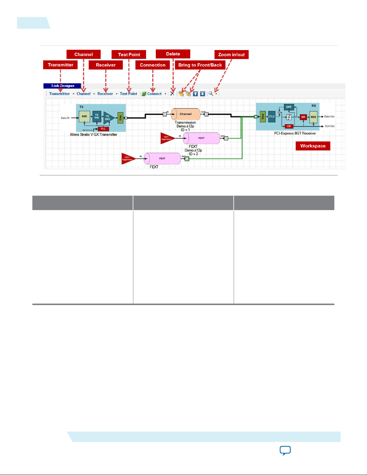
A link consists of a transmitter, a receiver, and one or more channel components. Select the transmitter,
receiver, and channel components from the menus at the top of the Link Designer workspace.
After the link components are placed into the workspace, click Connect to connect the components. In
connect mode, one or two connectors are shown on each component. Connect the link components by
dragging the line from one connector to another. Two types of connections are provided in Link
Designer: Right Angled Line and Straight Line. Right Angled Line is the default connection method. Test
Altera Corporation
Functional Description
Send Feedback
Page 9
UG-1146
2015.05.04
Constructing Communication Links in the Link Designer Module
points can be manually placed into the link by clicking Test Point and connecting to the desired location
in the link.
The following rules of link construction apply to the Link Designer module:
• A transmitter can only have one output port or connector
• A receiver can only have one input port or connector
• A channel component has one input and one output port
• A test point can only be connected to an input port
• A connection between two components can be established from an output port to an input port
• A transmitter cannot be connected directly to a receiver
A link establishment checking algorithm runs constantly in the background, checking whether a link is
established for simulations. When a link is established between a transmitter and receiver, the link lines
become bold and color-coded. Bold black lines indicate signal paths, green lines indicate crosstalk signal
paths, and purple lines point to test point port locations. The following figure shows an example link
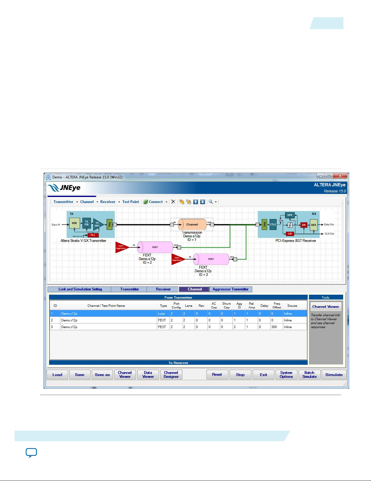
topology. A table of link components is displayed in the Channel tab for reference.
Figure 2-3: JNEye Link Designer with Channel Table
2-3
When a channel component (for example, a transmission line, connector, far-end crosstalk (FEXT), nearend crosstalk (NEXT), package, AC coupling capacitor, or shunt capacitor) is chosen, the Channel
Wizard helps you verify or set the channel configuration.
Functional Description
Send Feedback
Altera Corporation
Page 10
2-4
Constructing Communication Links in the Link Designer Module
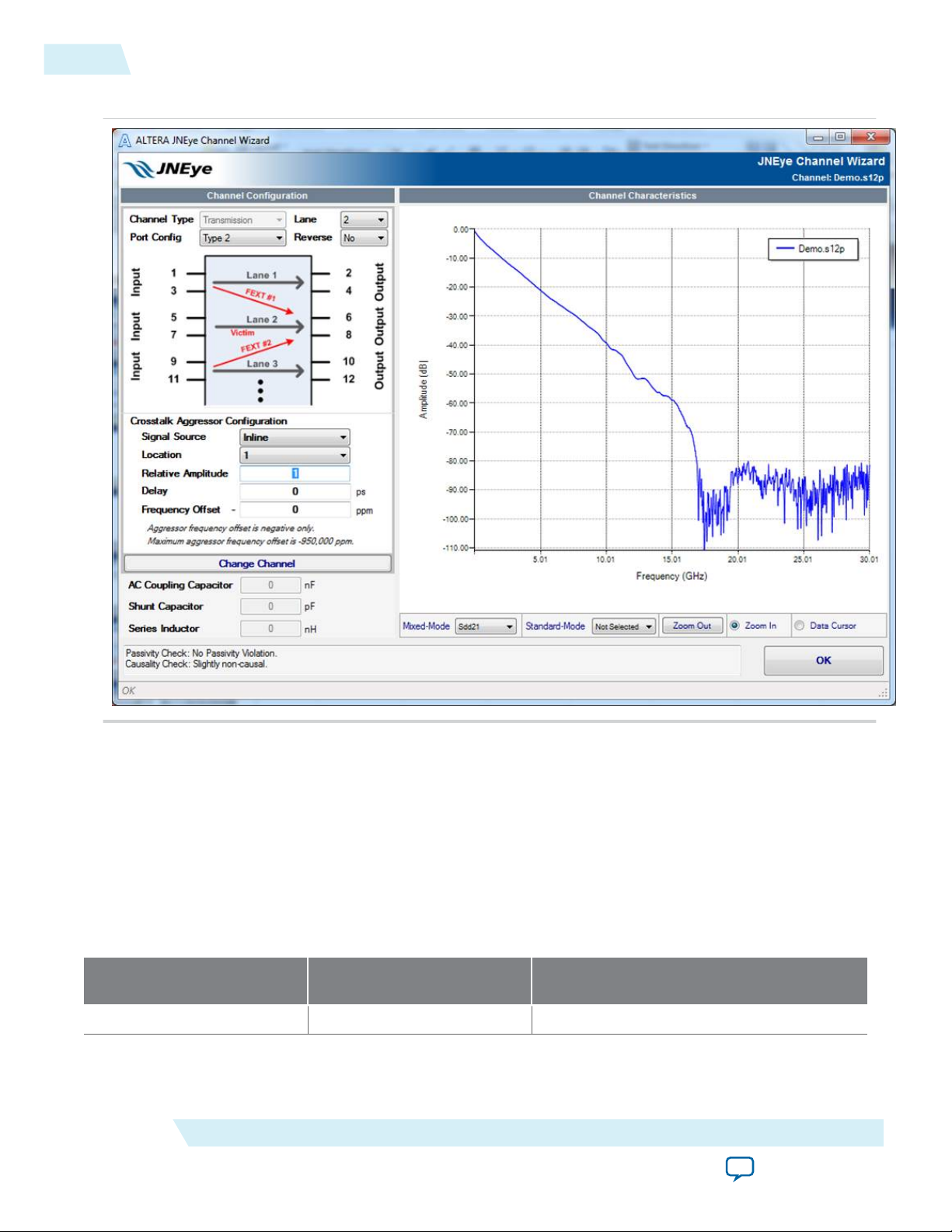
Figure 2-4: JNEye Channel Wizard
UG-1146
2015.05.04
The Channel Wizard displays the channel characteristics and allows you to verify the correctness of the
channel component, such as a component represented by an S-parameter. The Channel Wizard allows
you to select a channel type, port configuration, signal lanes (for multiple-lane S-parameters with eight
and more ports), crosstalk aggressor location (for multiple-lane S-parameters), aggressor, series
inductance value (in nH), AC coupling capacitor value (in nF), and shunt capacitance value (in pF). The
Channel Wizard checks the integrity of the channel component in terms of passivity and causality
characteristics. When the Channel Wizard detects passivity and causality violations, it displays messages
about the severeness of the violations in the text box on the left of the OK button. The levels of channel
integrity violation are listed in the following tables.
Table 2-2: Channel Passivity Check Results and Recommendations
Passivity Violation Check
Results
Impact on Link Simulation
Accuracy
No Passivity Violation No impact No action needed
Altera Corporation
Recommendations
Functional Description
Send Feedback
Page 11
UG-1146
2015.05.04
Constructing Communication Links in the Link Designer Module
2-5
Passivity Violation Check
Results
Slight Passivity Violation There may not be a noticeable
Impact on Link Simulation
Accuracy
effect in the simulation result
The channel model can be further
improved but the improvement in terms of
simulation results accuracy can be small.
Minor Passivity Violation There may be a noticeable
effect in the simulation result
The channel model can be further
improved. The differences in terms of
simulation results and accuracy are
expected.
Passivity Violation Simulation result will be
impacted
The channel model needs to be regenerated
(by design tools) or re-taken (by
instruments). The confidence of simulation
results using this channel model is low.
Table 2-3: Channel Causality Check Results and Recommendations
Causality Violation Check
Results
Impact on Link Simulation
Accuracy
Channel is causal No impact No action needed
Slight non-causal There may not be a noticeable
effect in the simulation result
The channel model can be further
improved but the improvement in terms of
simulation results accuracy can be small.
Recommendations
Recommendations
Somewhat non-causal There may be a noticeable
effect in the simulation result
The channel model can be further
improved. The differences in terms of
simulation results and accuracy are
expected.
Non-causal Simulation result will be
impacted
The channel model needs to be regenerated
(by design tools) or re-taken (by
instruments). The confidence of simulation
results using this channel model is low.
To select another S-parameter within the Channel Wizard, click Change Channel.
Altera recommends that you replace or change a channel with one of the same channel type. Link
Note:
Designer allows channel changing with different channel types, but you might see inconsistent
channel icons in the design workspace.
An existing channel can be changed by adding a new channel component or by modifying an existing
channel component. Right-click in the Link designer module and select Properties.
When using the package channel component, follow these guidelines:
• Package models should be placed next to the devices.
• Each device can have only one package model. Therefore, the external package model can only be used
when the device’s package type is “Custom”.
• The package model type is used by the simulation engine to identify the boundary of the devices and
generate a waveform for observation and analysis.
• The package model is treated the same way as the “Transmission” channel type. Therefore, use the
“Transmission” channel type even if the model represents a physical package (in your system) but it is
not a package of the TX and RX.
Functional Description
Send Feedback
Altera Corporation
Page 12
2-6
Link and Simulation Setting
Link and Simulation Setting
The Link and Simulation Setting tab sets the global link parameters and simulation configurations.
Figure 2-5: Link and Simulation Setting Tab
UG-1146
2015.05.04
The Link and Simulation Setting dialog box contains the following fields.
Data Rate
Link data rate is specified in Gbps.
Simulation Length
Simulation length is specified in the number of bits running at the specified data rate. Simulation length
should be at least 4096 bits. Altera recommends that the length is a power-of-2 factor for the best
computation efficiency. The simulation length does not apply in Statistical mode.
Simulation length is adjusted automatically to the closest power-of-2 factor.
Note:
Target BER
Target bit error rate is used to calculate the jitter and noise at low BER conditions. The methodology of
jitter and noise at low BER can be found in HST Jitter and BER Estimator Tool User Guide for Stratix IV
GT and GX Devices.
Altera Corporation
Functional Description
Send Feedback
Page 13

UG-1146
2015.05.04
Link and Simulation Setting
Test Pattern
Allows you to specify the test pattern used in the simulation. The following test patterns are available:
• PRBS-7, PRBS-9, PRBS-11, PRBS-15, PRBS-23, and PRBS-31
• The PRBS test patterns are generated using JNEye’s built-in pattern generator.
• If the whole PRBS pattern is shorter than the simulation length, the PRBS pattern is inverted and
repeated. The inversion is applied to achieve DC balance of the generated PRBS test pattern.
• If the PRBS patterns are longer than the simulation length, a partial test pattern of the PRBS pattern
is used. The default initial condition of PRBS test pattern generation is with logic 1s in all shift
registers for the valid PRBS patterns.
• The most commonly used PRBS test patterns are listed in the Test Pattern menu. Other PRBS test
pattern can be selected or configured in the Pattern Designer.
2-7
Functional Description
Send Feedback
Altera Corporation
Page 14
2-8
Link and Simulation Setting
• Pattern Designer—Allows you to specify your own custom test patterns. The following figure shows
the Pattern Designer user interface.
Figure 2-6: JNEye Pattern Designer
UG-1146
2015.05.04
Altera Corporation
The Pattern Designer includes the following test pattern generation methods:
• PRBS—Provides an extensive list of common PRBS test patterns. You can also specify custom
PRBS polynomials and seeds. The internal linear feedback shift register (LFSR) engine uses the
information to generate the desired test pattern. Other options include selecting how the test
pattern is repeated or extracted when the simulation length is longer or shorter than the generated
test patterns. There are two options for selecting the partial test patterns:
• Use First Part of Generated PRBS Sequence
• Include Longest Run-Length Bit Sequence—The longest run-length test pattern will be located
at the ending portion of the test bit sequence.
• Consecutive Bit Patterns—Defines the test patterns with repeating patterns.
• Clock—Generates a clock-like pattern.
• All 1's—Generates an all-ones test pattern that usually feeds into a coder or scrambler.
• All 0's—Generates an all-zeros test pattern that usually feeds into a coder or scrambler.
• Encoder and Scrambler—JNEye supports the following encoders and scramblers: 8B/10B, 64B/
66B, 64B/67B, and 128B/130B.
Functional Description
Send Feedback
Page 15
UG-1146
2015.05.04
Link and Simulation Setting
• Custom—Click the open-file dialog button to select a custom test pattern file.
Figure 2-7: Custom Test Pattern File Browser Button
The custom pattern files are in the following formats:
• Hexadecimal—Hexadecimal strings start with 0x. For example, a PRBS-7 test pattern can be
specified by 0x8cd501fbe7ae1ba62b05e3b64a4272d0. The custom file name must have a .hex
extension.
• Binary—Binary strings have a format such as "001000111…". Blank characters and new lines/
returns are allowed in the input binary string file. The custom file name must have a .bin extension.
2-9
Note:
The custom test pattern has a maximum text length of 262,142 characters (about 1M bits with a
hexadecimal text format or about 246K bits with a binary text format). Altera recommends that
the test pattern string (hexadecimal or binary) is specified in a single row without spaces,
especially for long custom test patterns. If a custom test pattern is input with multiple lines of
text, the line returns or end-of-line control characters on each line of text are counted as an item
or entry by the text parser.
Reference Clock
Specifies the reference clock that feeds into the transmitter. The supported clock frequencies are shown in
MHz. By default, the reference is assumed to be ideal without any noise or jitter. You can configure and
specify the reference clock characteristics by clicking Reference Clock Option.
The reference clock can be fed to a transmitter with or without enabling a phase-locked loop (PLL)
module. When the transmitter PLL is disabled or not present, the reference clock noise and jitter directly
affects the serial output signal.
With integer PLLs, JNEye supports an integer divider ratio between the data rate and the reference clock
frequency. If the ratio is not an integer, the reference clock frequency is rounded to the closest integerdivided-ratio frequency. The actual reference clock frequency used in the simulation is displayed in the
message box next to the pull-down menu. With fractional-N PLLs, fractional divider ratios are allowed.
In the simulation with specific transmitter devices, such as Arria 10 GX/SX/GT, Stratix V GT, Stratix V
GX, and Arria V GZ devices, the supported data rate to reference clock divider ratios are limited. If a
specific combination of data rate, PLL divider ratio, and reference clock frequency cannot be found, the
reference clock used in the simulation can be further adjusted.
Functional Description
Send Feedback
Altera Corporation
Page 16
2-10
Link and Simulation Setting
The reference clock frequencies listed are commonly used in most serial link protocols. If you cannot find
the exact reference clock frequency from the list, you can add your reference clock frequency with the
following procedure:
1. Close JNEye.
2. Navigate to the JNEye installation directory. Typically, JNEye is installed in C:\altera\15.0\jneye\.
3. Under the Database folder, find RefCLK_List.jnetxdata.
4. Edit the file by adding your desired reference clock frequencies.
5. Save the change and exit the editor.
6. Restart JNEye.
Reference Clock Option
The reference clock option user interface allows you to configure the characteristics of the reference clock
used in the simulation. The reference clock can be specified with the following methods:
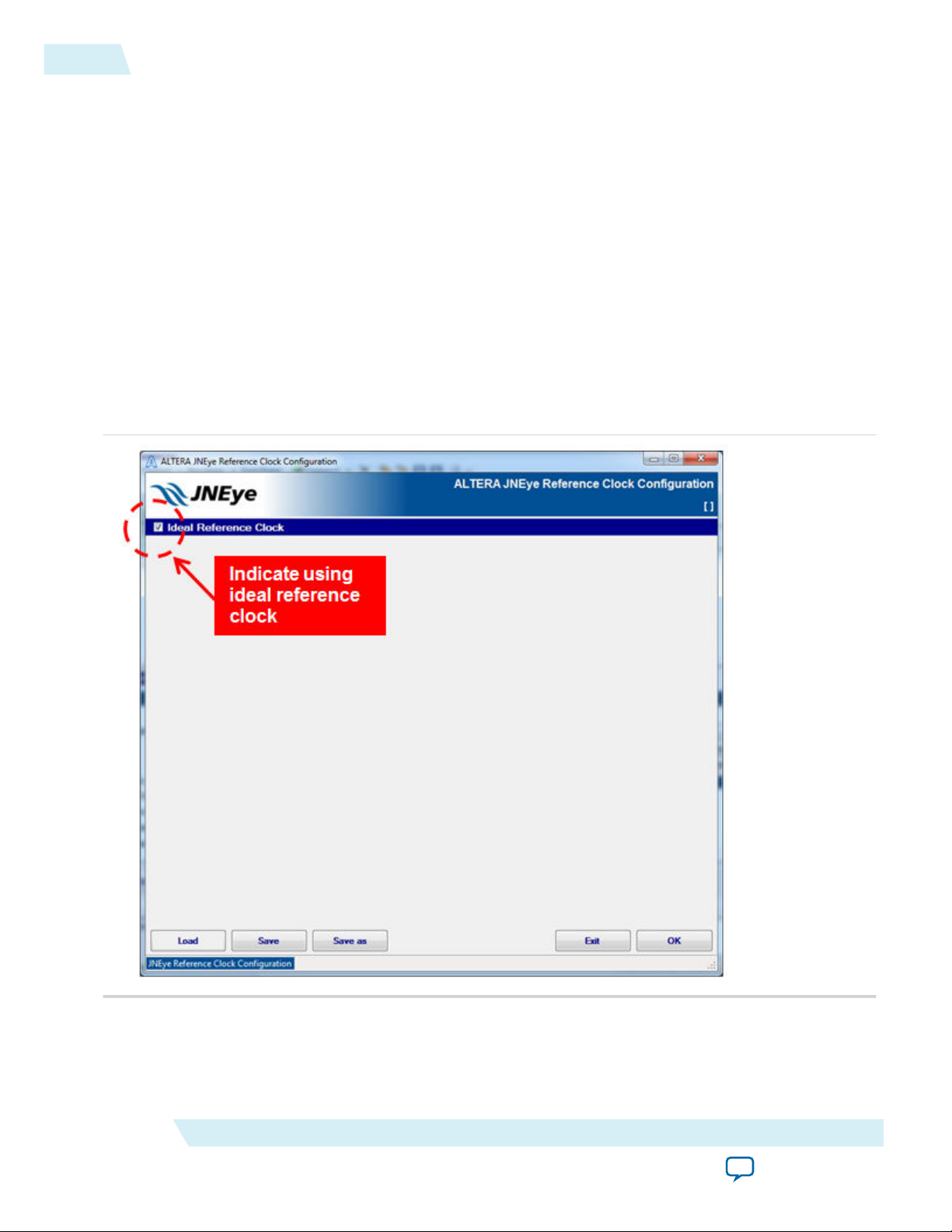
• Ideal Reference Clock—With this setting, the reference clock is ideal without any noise or jitter.
Figure 2-8: Ideal Reference Clock Setting
UG-1146
2015.05.04
Altera Corporation
Functional Description
Send Feedback
Page 17
UG-1146
2015.05.04
• Option 1: Reference Clock Jitter
Figure 2-9: Reference Clock Option 1: Reference Clock Jitter
Link and Simulation Setting
2-11
Functional Description
Send Feedback
Altera Corporation
Page 18

2-12
Link and Simulation Setting
Option 1 configures the reference clock with the following options:
• Random Jitter— Specify the frequency range (in ps).
UG-1146
2015.05.04
Note: Altera recommends that the maximum frequency range (f
reference clock frequency. If the f
linear extrapolation to calculate the phase noise at f
is less than the reference clock frequency, JNEye uses
MAX
MAX
) of the phase noise be set to the
MAX
, which can lead to inaccurate results.
• Periodic Jitter Type—Specify the shape profile, frequency (in Hz), and amplitude (in ps). The shape
profile can be:
• Triangle
• Hershey with programmable Hershey shape parameter
• Sharkfin with programmable Sharkfin shape parameter
• Sinusoidal
• Spurs—Specify clock spectrum spurs with individual frequency (in Hz) and amplitude (in dBc). For
example, if the reference clock has three spurs: –110 dBc at 100 KHz, –90 dBc at 1 MHz, and –80 dBc
at 10 MHz, you can input the following text into the Spurs text box:
100e3 -110
1e6 -90
10e6 -80
• Spur Phase Offset
Use the Spur Phase Offset pull-down menu to configure the initial phase of spur noises. The options
are:
• Auto—JNEye automatically selects the default initial spur noise phase. The default initial spur
phase is 0 rad.
• Random—JNEye randomly sets the initial spur noise phases.
• Zero—JNEye sets the initial spur noise phase to 0 rad.
• Specified—You can manually specify the initial spur phase individually by adding the phase value
after the amplitude value. The following example shows the initial spur noise phases are 1.0, 2.0,
and 3.0 rad.
Altera Corporation
100e3 -110 1.0
1e6 -90 2.0
10e6 -80 3.0
Functional Description
Send Feedback
Page 19
UG-1146
2015.05.04
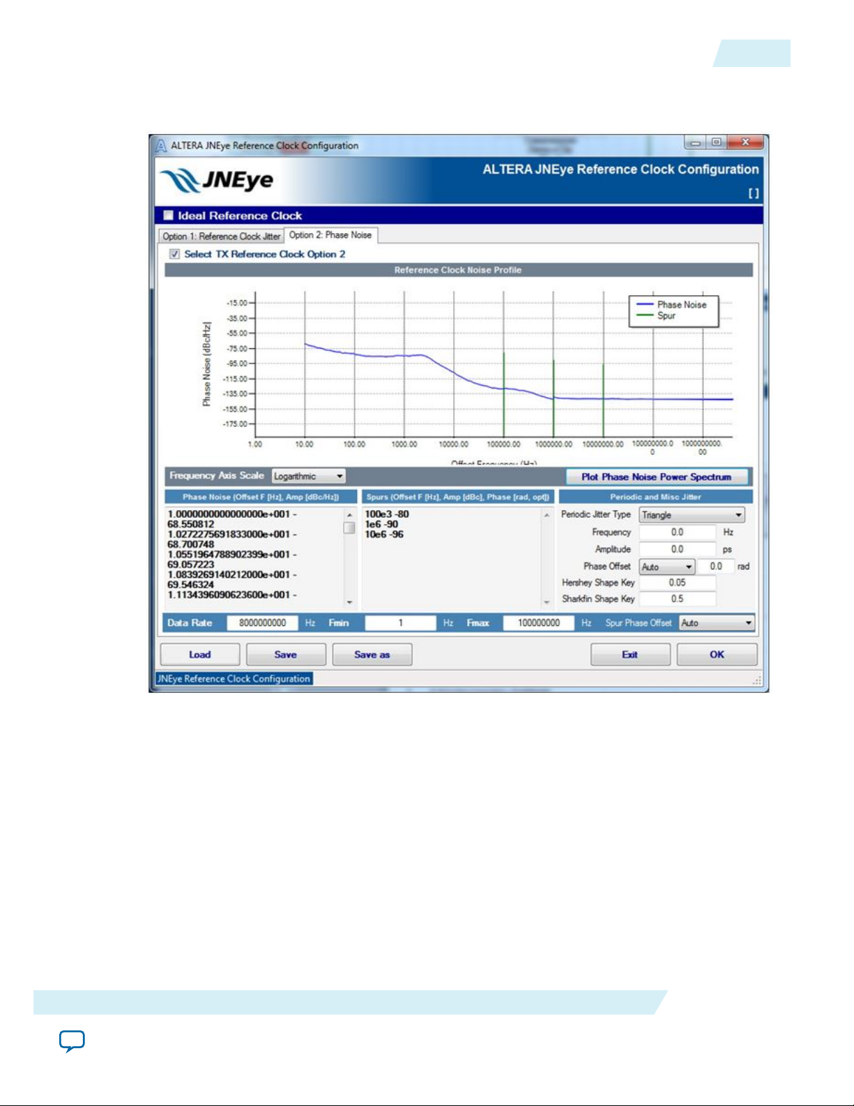
• Option 2: Phase Noise
Figure 2-10: Reference Clock Option 2: Phase Noise
Link and Simulation Setting
2-13
Functional Description
Send Feedback
Altera Corporation
Page 20

2-14
Link and Simulation Setting
UG-1146
2015.05.04
Option 2 configures the reference clock with the following options:
• Phase Noise—Specify reference clock jitter using a phase noise profile. Reference clock phase noise is
specified with the noise power spectrum described with frequency and amplitude. The above figure
demonstrates a phase noise profile with a measured reference clock phase noise data set.
Note: Altera recommends that the maximum frequency range (f
reference clock frequency. If the f
MAX
linear extrapolation to calculate the phase noise at f
• Spurs—Specify clock spectrum spurs with individual frequency (in Hz) and amplitude (in dBc). For
example, if the reference clock has three spurs: –80 dBc at 100 KHz, –90 dBc at 1 MHz, and –96 dBc at
10 MHz, you can input the following text into the text box:
100e3 -80
1e6 -90
10e6 -96
• Spur Phase Offset—Same as in Option 1 Reference Clock Jitter.
• Periodic Jitter Type—Same as in Option 1 Reference Clock Jitter.
• Plot / Update Plot—You can plot the input phase noise and spurs in the plotting area and confirm the
reference clock characteristics.
Link Optimization Method
JNEye can find optimal transmitter and receiver equalization settings with a user-specified link configura‐
tion.
The TX/RX joint link optimization function is specific to JNEye and may not be supported by the
Note:
transmitter and receiver devices.
Table 2-4: Link Operation Modes Supported by JNEye
) of the phase noise be set to the
MAX
is less than the reference clock frequency, JNEye uses
, which can lead to inaccurate results.
MAX
Transmitter Mode Receiver Mode Notes
Manual Manual Both TX and RX equalizations are manually set.
Auto /
Auto with Manual
Manual JNEye finds optimal TX equalization setting. RX EQ
setting is manually set.
Starting Point
Manual Auto TX EQ is manually set. JNEye finds optimal RX EQ
setting.
Auto /
Auto JNEye finds both TX and RX EQ settings.
Auto with Manual
Starting Point
JNEye has four link optimization methods for finding the optimal link setting, such as a transmitter preemphasis and receiver CTLE and DFE with a given link configuration.
Altera Corporation
Functional Description
Send Feedback
Page 21

UG-1146
2015.05.04
Link and Simulation Setting
2-15
• FIR => CTLE => DFE— (default) Optimizes the link performance by finding the optimal transmitter
setting, receiver equalization setting, or both. This method prioritizes the transmitter equalization,
such as pre-emphasis, de-emphasis, or FIR-based, over receiver equalization schemes. However, the
optimization algorithm is also capable of detecting and utilizing optimal receiver equalization. In
practice, this usually implies that most of the "heavy-lifting" in channel compensation is performed by
the transmitter equalization.
• FIR => CTLE & DFE—Extends the FIR => CTLE =>DFE method by enabling RX DFE (Decision
Feedback Equalizer) when RX optimization is performed. This method exploits DFE capabilities by
possibly reducing the channel compensation from CTLE (depending on the channel characteristics).
• CTLE => FIR => DFE—Prioritizes the receiver's CTLE capability over the transmitter's equalization.
Most of the channel compensation is performed by the receiver's CTLE while the TX equalization
provides additional compensation if needed. RX DFE is adapted in the final stage. This method is
supported in non-IBIS-AMI devices. For Altera transmitters, you can manually set initial TX FIR
configurations so the link optimizations can yield better solutions more quickly when the initial
conditions are proper.
• CTLE => FIR & DFE—Extends the CTLE => FIR => DFE method by joint-optimizing TX pre-
emphasis/FIR and RX DFE. This method allows co-optimization between the TX FIR and RX DFE.
For Altera transmitters, you can manually set the initial TX FIR configurations so the link optimiza‐
tions can yield better solutions more quickly when the initial conditions are proper.
Use the following guidelines for choosing the best link optimization method:
• FIR => CTLE => DFE is a good choice for most applications or channels for time efficient link
optimizations. It is the default link optimization method in JNEye.
• For heavy insertion loss channels such as when insertion loss > 25 dB at Nyquist frequency, FIR =>
CTLE => DFE provides good coverage.
• For strong impedance discontinuities, CTLE => FIR => DFE methods provide better performance in
general.
• For large crosstalk noises, choose FIR => CTLE & DFE for high loss channels or CTLE => FIR & DFE
for moderate loss applications.
Notes:
• JNEye supports link optimization for selected IBIS-AMI models for the link optimization modes and
the methods shown above. Refer to the IBIS-AMI model support sections for details.
• For a transmitter equalization sweep simulation, JNEye provides batch simulation capability using the
JNEye Batch Simulation Controller tool. Refer to the JNEye Batch Simulation Controller section for
details.
FOM of Link Optimization
Use this menu to select the figure of merit (FOM) for optimizing the serial link. There are three options:
Area, Width, and Height. The signal conditioning mechanisms, which include transmitter pre-emphasis,
de-emphasis, and receiver equalizers, use these selections to optimize the waveform so that it has the best
eye diagram opening in terms of area, width, or height.
Compliance Mask
JNEye plots link compliance eye diagram masks after the simulations are completed. Use a compliance
mask to examine whether the waveform or eye diagram meets the receiver's requirements at certain
conditions (such as BER target). PCI-Express 8GT receiver eye masks are provided.
Device intrinsic jitter can be included in the link simulation by using the Characterization Data
Note:
Access function in JNEye. When both transmitter and receiver jitter are extracted from the
Characterization Data Access and included in the simulation, the simulation results at the end of
Functional Description
Send Feedback
Altera Corporation
Page 22

2-16
Link and Simulation Setting
the link represent the link margin at the specified bit error rate (BER) target. Link margin
simulation using transmitter and receiver jitter provides better accuracy than the conventional eye
mask method.
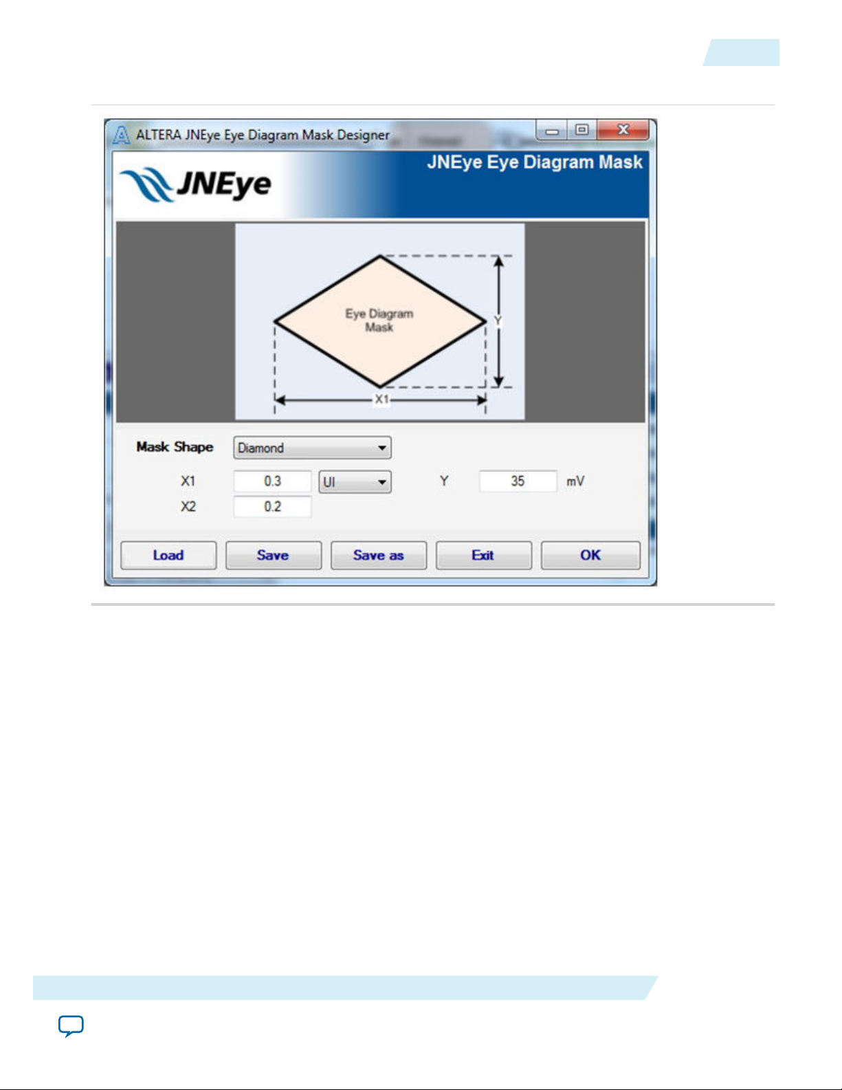
Eye Diagram Mask Designer
JNEye supports custom eye diagram mask definition. When the Eye Diagram Mask Designer option is
selected, the custom eye diagram mask configuration window opens. You can then specify the dimension
of the eye diagram mask. The custom eye diagram mask is used in the simulation. Two eye diagram mask
types are supported:
Figure 2-11: Hexagon-Shaped Eye Diagram Mask Editor
UG-1146
2015.05.04
Altera Corporation
Functional Description
Send Feedback
Page 23
UG-1146
2015.05.04
Figure 2-12: Diamond-Shaped Eye Diagram Mask Editor
Link and Simulation Setting
2-17
A custom eye diagram mask can be saved and loaded for future use.
Project Name
A user-defined name for the current task/project. Currently, the session name is the saved user configura‐
tion file name when the simulation configuration is saved.
Notes:
• The simulation results are automatically written to a directory with the same project name.
• The location of the output directory can be configured as a) the same location as the project configura‐
tion file (.jne/.jneschm) (this is the default), or b) a location you specify in the System Options. Refer to
the System Options section for details.
Simulation Mode
JNEye provides three simulation modes (statistical, full waveform, and hybrid) to meet your simulation
and link analysis preferences and needs. Hybrid mode is the default.
Functional Description
Send Feedback
Altera Corporation
Page 24

2-18
Link and Simulation Setting
Table 2-5: Simulation Modes
PDF = Probability Density Function
Statistical Mode Full Waveform Mode Hybrid Mode (Default)
Simulation Method Statistical Method Time-domain Method Time-domain and
Statistical Methods
UG-1146
2015.05.04
Jitter Injection and
Simulation
Statistical Domain
(PDF- based)
Time Domain Mixed Domain (Time
Domain and PDFbased)
Noise Injection and
Simulation
Statistical Domain
(PDF- based)
Time Domain Mixed Domain (Time
Domain and PDFbased)
Simulation Speed
Fast Slow Optimal
(to meet your specified
BER target)
Accuracy Lower Best Optimal
Recommended
Simulation Length
N/A (You do not need to
specify simulation length
>500,000 bits ~60,000 bits
in statistical mode.)
Further information and comparisons among the three simulation modes can be found in the following
papers:
1. Comparison of Two Statistical Methods for High-Speed Serial Link Simulation by M. Shimanouchi, M.
Li, and H. Wu. DesignCon, 2013, Santa Clara, CA.
2. Advancements in High-Speed Link Modeling and Simulation by M. Li, M. Shimanouchi, and H. Wu.
IEEE Custom Integrated Circuits Conference, 2013.
3. High-Speed Link Simulation Strategy for Meeting Ultra Long Data Pattern under Low BER Require‐
ments by H. Wu, M. Shimanouchi, and M. Li, DesignCon, 2014, Santa Clara, CA.
Output Options
• Data Viewer—When simulation is complete, a new JNEye Data Viewer opens and the results are
• Data Viewer with Image Output—When simulation is complete, all the simulation results are also
Altera Corporation
shown. The simulation results can be loaded and viewed at a later time with JNEye Data Viewer.
saved as image files that can be used in documentation. JNEye supports three image output options:
PNG, JPEG, and GIF. The saved images are located in the same directory as the simulation results for
each project.
Functional Description
Send Feedback
Page 25

UG-1146
2015.05.04
Link and Simulation Setting
Test Point Options
JNEye provides the following default test point options:
• Data Latch Only—(default option) Simulation results at the data latch will be saved and displayed.
Data latch can be at DFE output, CTLE output, or input stage of receiver depending on the link or
device configuration. Custom test points will be neglected and the simulation results at test points will
not be shown.
• TX/Channel/CTLE-/DFE-Latch—JNEye automatically sets up to four test points for the link:
• Transmitter output—If a transmitter package model is present (for example, the package model is
embedded, as in Altera devices and PCI-Express 8GT) or external (for example, using the "Custom"
package option), the output appears after the package model. If no package model is present, the
output appears at the transmitter output.
• Channel output—The second test point is at the end of channels.
• CTLE output—If you enable the receiver CTLE, the third test point is at the output of the CTLE.
• DFE output—The fourth test point is at the output of the receiver DFE.
2-19
Note:
Custom test points are neglected with this test point option.
• Custom Test Point and Data Latch—JNEye plots the output at custom test points and the final data
latch point.
Probe Type
JNEye provides two type of probes:
• Ideal—With an ideal probe, the waveform, signal, or eye diagram is plotted by assuming that the link
is terminated with an ideal 50 ohms termination at the probe location.
• High-Impedance—With a high-impedance probe, the waveform, signal, or eye diagram is plotted by
emulating a high-impedance probe sensing the probe location.
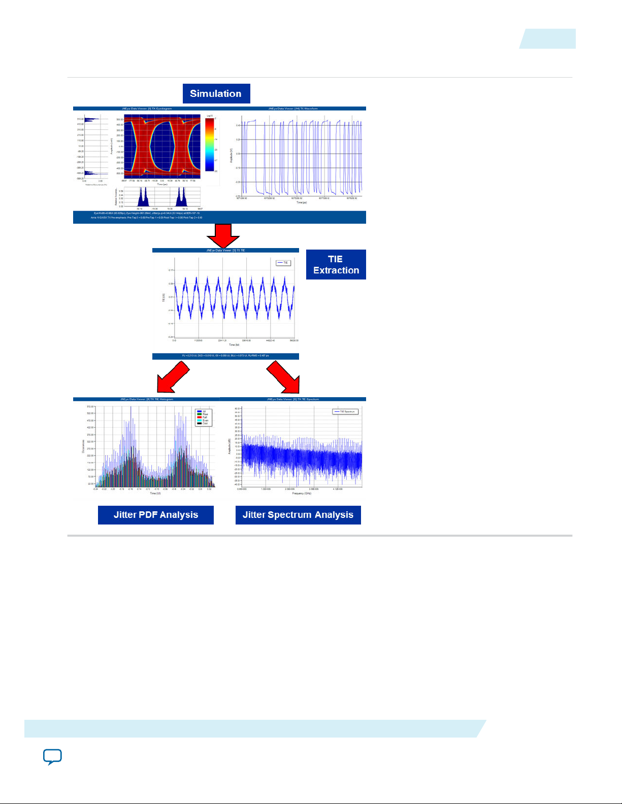
Jitter Analysis Options
JNEye can perform jitter decomposition and analysis on a waveform at specified test points. The jitter
analysis feature is in the beta testing stage in the JNEye 15.0 release.
• Disable—Jitter analysis is disabled.
• Jitter Component—Using proprietary algorithms, JNEye performs a series of spectrum and
probability density function (PDF) analyses on the time-interval-error (TIE) record of the simulated
waveforms. The jitter decomposition algorithms extract various jitter components as shown in the
following figure.
Functional Description
Send Feedback
Altera Corporation
Page 26
2-20
Link and Simulation Setting
Figure 2-13: Jitter Component Supported in JNEye Jitter Analysis Feature
UG-1146
2015.05.04
The jitter decomposition process (conceptual) is shown in the following figure.
Altera Corporation
Functional Description
Send Feedback
Page 27
UG-1146
2015.05.04
Figure 2-14: Jitter Decomposition Process (Conceptual)
Link and Simulation Setting
2-21
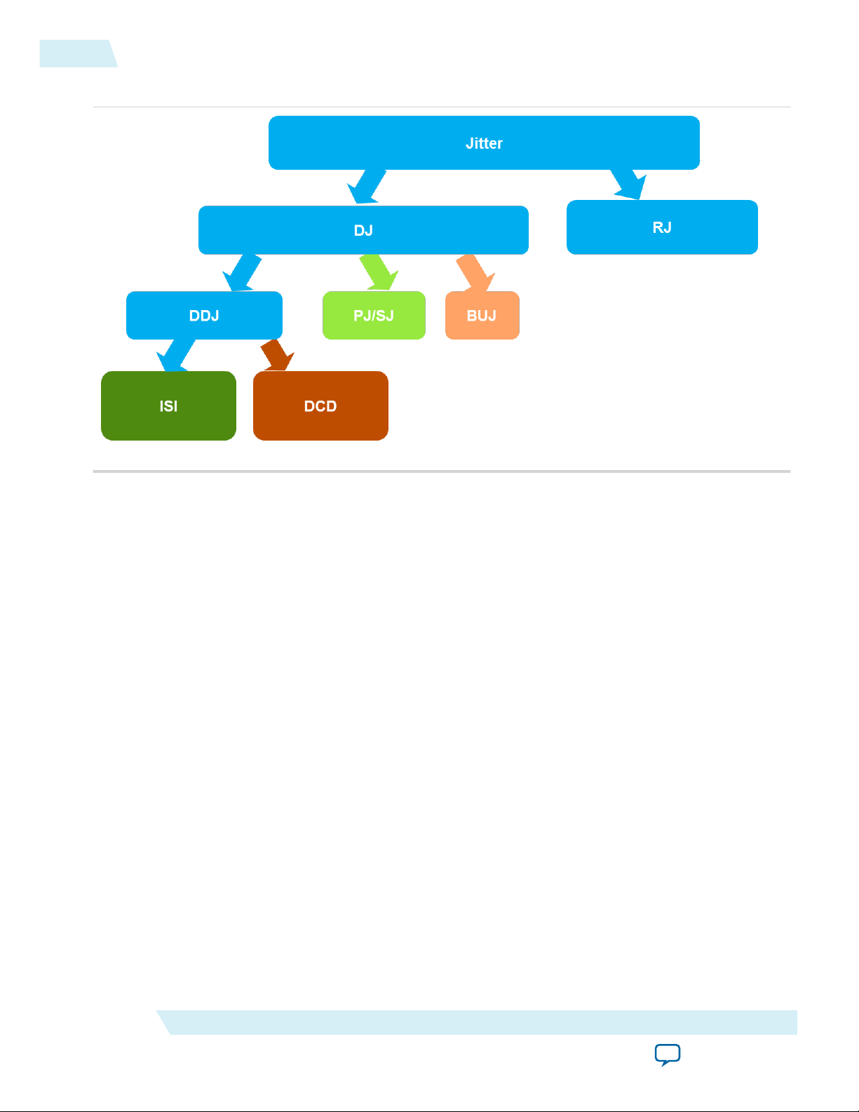
In JNEye 15,0, the following jitter components are extracted and reported:
• PJ—Periodic jitter (peak-peak)
• DCD—Duty cycle distortion (peak-peak)
• ISI—Inter-symbol interference (peak-peak)
• BUJ—Bounded uncorrelated jitter (peak-peak)
• RJ-RMS—Random jitter (RMS)
Note:
Related Information
• JNEye Batch Simulation Controller on page 2-129
• HST Jitter and BER Estimator Tool User Guide for Stratix IV GT and GX Devices
Functional Description
Send Feedback
In JNEye 15.0, jitter analysis is available in Hybrid simulation mode only.
Altera Corporation
Page 28
2-22
Transmitter Setting
Transmitter Setting
The transmitter generates signals based on the transmitter clock and test pattern conditions.
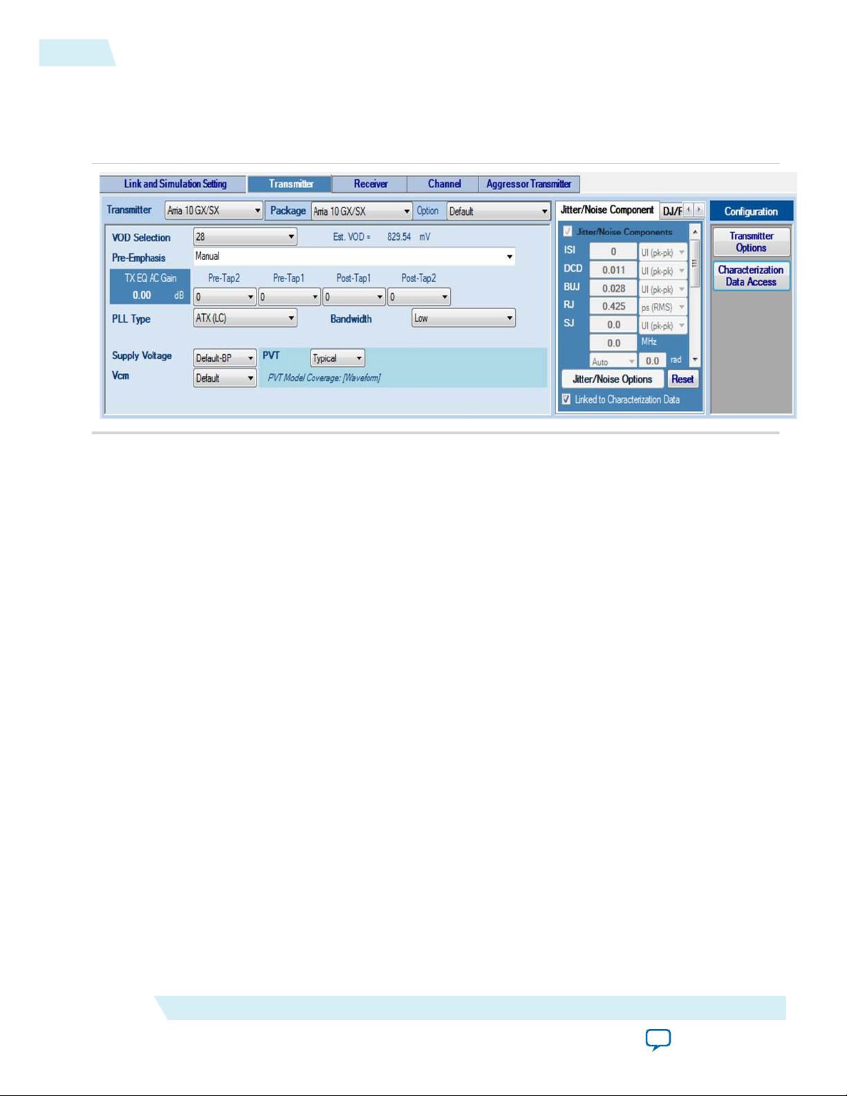
Figure 2-15: JNEye Transmitter Settings
UG-1146
2015.05.04
Transmitter
The following transmitter types are supported:
• Stratix V GX
• Arria V GZ
• Arria 10 GX/SX
• Arria 10 GT
• IBIS-AMI
• Custom
• PCI Express 8GT
The transmitter type determines what other transmitter settings you can select. When a transmitter is
chosen, it is automatically inserted into the Link Designer, ready to connect to other link components.
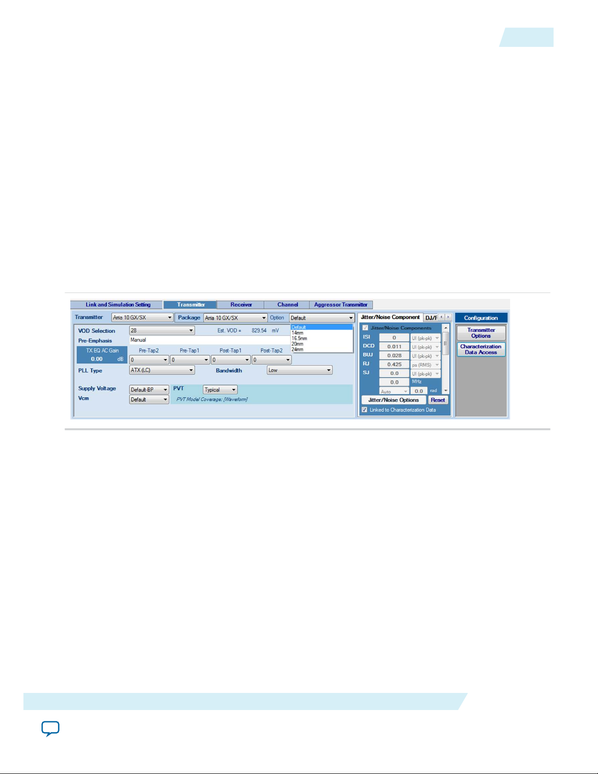
Package
Select a package type for the transmitter device. For Altera products and IBIS-AMI models, the package
models are included in the device models. For Custom devices, the package model is specified in the
channel setting. When you select the Custom package type (for any transmitter devices), the embedded
package model (if available) is disabled. You can then add a channel component (such as an S-parameter)
with type Package in the Link Designer workspace. The Custom package model must be placed next to the
transmitter module so it can be simulated and analyzed correctly. If you choose the Custom package type
but do not add a channel component with Package type to the Link Designer workspace, the transmitter is
simulated without any package model.
Altera Corporation
Functional Description
Send Feedback
Page 29
UG-1146
2015.05.04
JNEye comes with the following transmitter package models:
• Stratix V GX
• Arria V GZ
• Stratix V GT
• Arria 10 GX/SX
Options: Additional package models (shown in the following figure) are available for Arria 10 devices.
The package model is specified as its trace length inside the package. These models are chosen to cover
the range of package trace lengths in Arria 10 transceiver transmitters.
• Default—The default package model is same as the 14 mm option
• 14mm
• 16.5mm
• 20mm
• 24mm
Contact your Altera’s representative if you would like to know how to pair your design with the Arria
10 package model options.
Figure 2-16: Arria 10 Transmitter Package Options
Transmitter Setting
2-23
• Arria 10 GT—Same options as Arria 10 GX/SX
• PCI-Express 8GT
VOD Selection
Select the VOD (differential output voltage) for the transmitter. VOD selections can be either by voltage
level or by index, depending on the transmitter selected. For supported devices, the target VOD value is
displayed in the Transmitter tab page. The VOD value depends on the device type, supply voltage, and
PVT.
Functional Description
Altera Corporation
Send Feedback
Page 30

2-24
Transmitter Setting
Pre-Emphasis
Select or specify the transmitter pre-emphasis, de-emphasis, or TX-FIR configuration in one of the
following modes:
• Auto—JNEye uses its link optimization algorithm to find the optimal transmitter FIR settings.
• Auto with Manual Starting Point—Specify the initial TX pre-emphasis or FIR configuration. JNEye’s
link optimization engine uses the TX settings as initial conditions.
• Manual—For non-Altera devices, you can manually input the tap coefficients. For Altera devices,
select individual FIR levels from the menus for each FIR tap. The FIR selection for Altera devices is
VOD dependent. Therefore, changing the VOD or device type can reset the TX FIR menu contents.
For a generic transmitter type, a set of typical FIR coefficients is included in the pull-down menu.
• Off
Estimated TX EQ AC Gain
Select pre-tap and post-tap values to estimate the AC gain in dB scale. The TX EQ AC gain is calculated as
the gain between the DC (0 Hz) and the Nyquist frequency of the link, assuming a FIR type of transmitter
pre-emphasis scheme.
Note:
This is a rough analytical estimate of TX EQ AC gain that may differ from the actual AC gain
generated by the transmitter.
UG-1146
2015.05.04
PLL Type and Bandwidth
Select the type and bandwidth of the PLL used in the transmitter to generate the transmitter clock.
• Ideal Clock—The default PLL setting. The PLL is disabled and the clock is passed from the external
reference clock.
• For Altera transmitters, PLL models and configurations are automatically set based on the following
settings:
• Data rate
• Reference clock frequency
• Oscillator type:
• Stratix V GX and Arria V GZ—ATX (LC) or CMU
• Stratix V GT—ATX (LC)
• Arria 10 GX/SX/GT—ATX (LC), Fractional PLL, or CMU
• PLL bandwidth
• Altera transmitter PLL configurations such as internal divider ratios
Altera recommends that you follow Altera’s reference clock selection and PLL configurations
recommendations when setting up the transmitter PLL. Without following the reference clock and
PLL guidelines, you might operate and simulate an unstable PLL and see unexpected results.
• For Custom transmitters, PLL models and configuration are set automatically based on settings
similar to that of Altera PLLs while more comprehensive PLL configuration capabilities are under
development. With custom transmitters, the VCO can be either LC type or ring oscillator (Ring) type.
More PLL to reference clock divider ratios are supported in the custom PLL type. Follow Altera's PLL
and reference clock guidelines when setting up transmitter PLLs to avoid unexpected results.
• PLL is currently not supported for IBIS-AMI transmitters.
Altera Corporation
Functional Description
Send Feedback
Page 31

UG-1146
2015.05.04
Transmitter Setting
Supply Voltage
For supported devices, you can choose the supply voltage. In JNEye 15.0, the Arria 10 GX/SX/GT
transmitter model provides the following supply voltages:
• Default-BP—Supply voltage for backplane applications that have a dependency on the data rate
setting
• Default-C2C—Supply voltage for chip-to-chip applications that have a dependency on the data rate
setting
• 0.9 V (Arria 10 GX/SX/GT)
• 1.0 V (Arria 10 GX/SX/GT)
• 1.1 V (Arria 10 GT)
V
cm
Vcm is the common voltage of the transmitted signal.
PVT
Select the process, voltage, and temperature (PVT) models for the selected transmitter device. PVT model
support varies depending on device type, device data availability, and model coverage. A message is
shown on the Transmitter tab page to indicate the PVT model coverage. Transmitter PVT model coverage
and conditions are shown in the following table.
2-25
Table 2-6: Transmitter PVT Model Coverage
Transmitter Type Waveform PVT Model Jitter/Noise PVT Model
Stratix V GX Typical Process: Typical/Fast/Slow Voltage:
Typical/High/Low Temperature:
–40°C to 100°C
Arria V GZ Typical Process: Typical/Fast/Slow Voltage:
Typical/High/Low Temperature:
–40°C to 100°C
Stratix V GT Typical Process: Typical/Fast/Slow Voltage:
Typical/High/Low Temperature: 0°C
to 100°C
Arria 10 GX/SX Typical/Fast/Slow Typical
Arria 10 GT Typical/Fast/Slow Typical
IBIS-AMI Provide by IBIS-AMI
Provide by IBIS-AMI model
model
Custom None None
PCI-Express 8GT None None
JNEye to Quartus II Parameter Translation for Arria 10 GX/SX/GT Transmitters
The following table provides a translation from JNEye Arria 10 GX/SX/GT transmitter parameter names
to the equivalent Quartus II parameter names. Use the Quartus II software to transfer optimum device
settings from a JNEye simulation to an actual device configuration.
Functional Description
Send Feedback
Altera Corporation
Page 32

2-26
Jitter/Noise Component
Table 2-7: JNEye to Quartus II Parameter Translation for Arria 10 GX/SX/GT Transmitters
JNEye Name Quartus II Name
Vod Selection Transmitter Output Swing Level
Post-Tap 1
(1)
Transmitter Pre-Emphasis First Post-Tap
Magnitude
Post-Tap 2
(1)
Transmitter Pre-Emphasis Second Post-Tap
Magnitude
Pre-Tap 1
Pre-Tap 2
(1)
(1)
Transmitter Pre-Emphasis First Pre-Tap Magnitude
Transmitter Pre-Emphasis Second Pre-Tap
Magnitude
Sign of Post-Tap 1
(1)
Transmitter Pre-Emphasis First Post-Tap Polarity
(2)
UG-1146
2015.05.04
(1)
(1)
(1)
Transmitter Pre-Emphasis Second Post-Tap
Polarity
(2)
Transmitter Pre-Emphasis First Pre-Tap Polarity
Transmitter Pre-Emphasis Second Pre-Tap
Polarity
(2)
Quartus II PLL Type
• Arria 10 Transceiver ATX PLL
• Arria 10 fPLL
• Arria 10 Transceiver CMU PLL
Sign of Post-Tap 2
Sign of Pre-Tap 1
Sign of Pre-Tap 2
PLL Type
• ATX(LC)
• Fractional PLL
• CMU
PLL Bandwidth Bandwidth in PLL Configuration Options in
selected PLL type
Jitter/Noise Component
The Jitter/Noise panel allows you to input or import jitter and noise parameters. JNEye provides extensive
transmitter jitter and noise modeling and configuration capabilities.
The following figure shows the jitter decomposition diagram and the breakdown of jitter components.
(2)
(1)
In JNEye when Pre-emphasis is selected as Manual or Auto with Manual Starting Point
(2)
“0” = non-inverted which is positive tap selections in JNEye; “1” = inverted which is negative tap
selections in JNEye.
Altera Corporation
Functional Description
Send Feedback
Page 33

UG-1146
2015.05.04
Figure 2-17: Transmitter Jitter Decomposition
Jitter/Noise Component
2-27
Table 2-8: Transmitter Intrinsic Jitter and Noise Types
Name Description Unit Support
in JNEye
DJ Deterministic
Jitter
ISI Inter-Symbol
Unit Interval
Yes DJ can be generated using a uniform distribution,
(UI)
UI Yes ISI can be generated using a uniform distribution,
Interference
Comments
dual-Dirac, or truncated Gaussian method. Select
the DJ generation method in the Transmitter
Jitter/Noise Options Window. The default DJ
method is dual-Dirac. DJ consists of periodic jitter,
bounded uncorrelated jitter, inter-symbol interfer‐
ence, and duty-cycle distortion. The DJ value is
used in the simulation when the DJ/RJ-DN/RN
method is selected.
dual-Dirac, or truncated Gaussian method. Select
the ISI generation method in the Transmitter
Jitter/Noise Options Window. The default ISI
method is dual-Dirac.
Functional Description
Send Feedback
Altera Corporation
Page 34

2-28
Jitter/Noise Component
UG-1146
2015.05.04
Name Description Unit Support
in JNEye
DCD Duty Cycle
UI Yes The DCD parameter models two types of jitter:
Distortion
BUJ Bounded
UI Yes Same as Deterministic Jitter. The default BUJ
Uncorrelated
Jitter
RJ Random Jitter UI-RMS or ps-
Yes RJ is assumed to be Gaussian. RJ can be specified in
RMS
SJ Sinusoidal
Jitter
Amplitude: UI
Frequency:
Yes Sinusoidal jitter can be specified with amplitude and
MHz
Comments
Positive pulse width jitter (PPWJ) and Clock DCD.
The PPWJ shortens or lengthens the logic 1
waveform. The Clock DCD emulates distorted clock
waveform effects on the transmitter output
waveform. You can select the DCD generation
method in the Transmitter Jitter/Noise Options
Window. The default DCD method is PPWJ –
(shortened positive waveform).
method is Uniform distribution.
either pico-second (ps-RMS) or UI-RMS.
frequency.
DN Deterministic
Noise
mV Yes DN can be generated using a uniform distribution,
dual-Dirac, or truncated Gaussian method. You can
select the DN generation method in the
Transmitter Jitter/Noise Options Window. The
default DN method is uniform.
BUN Bound
Uncorrelated
Noise
mV Yes Same as DN. The default method is Truncated
Gaussian method with a Peak-to-RMS ratio of 14.
You can select the BUN generation method and
parameters in the Transmitter Jitter/Noise
Options Window.
RN Random Noise mV-RMS Yes RN is assumed to be Gaussian.
Altera Corporation
Functional Description
Send Feedback
Page 35

UG-1146
2015.05.04
Jitter/Noise Component
2-29
Name Description Unit Support
in JNEye
Jitter PDF Jitter
Probability
Density
Function
(PDF)
Jitter
amplitude,
Probability
(Jitter
amplitude can
be in absolute
time or UI
(unit interval)
unit)
Comments
Yes Jitter PDF defines the jitter probability density
function. The input format is jitter amplitude in
second and probability. The following is a jitter PDF
example:
-5e-12 1e-10
-4e-12 3e-7
-3e-12 1e-4
-2e-12 1e-2
-1e-12 0.29
0 0.4
1e-12 0.29
2e-12 1e-2
3e-12 1e-4
4e-12 3e-7
5e-12 1e-10
Noise
PDF
Noise
Probability
Density
Function
Noise
amplitude,
Probability
Yes Noise PDF defines the noise probability density
function. The input format is Noise amplitude in
volt and probability. The following is a noise PDF
example:
-50e-3 1e-10
-40e-3 3e-7
-30e-3 1e-4
-20e-3 1e-2
-10e-3 0.29
0 0.4
10e-3 0.29
20e-3 1e-2
30e-3 1e-4
40e-3 3e-7
50e-3 1e-10
Click Jitter/Noise Options to further configure each jitter and noise type. There are two jitter/noise
modes for JNEye’s transmitters: Jitter/Noise Component mode and DJ/RJ-DN/RJ mode. Only one jitter/
noise mode is active at a time and you must determine which mode to use in your simulations.
Functional Description
Send Feedback
Altera Corporation
Page 36

2-30
Jitter/Noise Component
• Jitter/Noise Component mode—JNEye uses a flat jitter/noise structure that assumes no overlapping
among all the jitter and noise components. Avoid double counting when inputting or importing jitter/
noise figures. In the following figure, there are six specific jitter components: DCD, ISI, SJ, BUJ, RJ,
and jitter PDF. The noise components DN, BUN, RN, and noise PDF must also be specified separately.
Figure 2-18: Specifying Transmitter Jitter and Noise in Jitter/Noise Mode
Figure 2-19: Transmitter Jitter/Noise Configuration in Jitter/Noise Component Mode
UG-1146
2015.05.04
Altera Corporation
Functional Description
Send Feedback
Page 37

UG-1146
2015.05.04
Jitter/Noise Component
• DJ/RJ-DN/RJ mode—All deterministic jitter/noise components are included in DJ and DN.
Figure 2-20: Specifying Transmitter Jitter and Noise in DJ/RJ-DN/RJ Mode
Figure 2-21: Transmitter Jitter/Noise Configuration in DJ/RJ-DN/RJ Method
2-31
Functional Description
Send Feedback
Altera Corporation
Page 38

2-32
Transmitter Options
Note: Jitter specified in the Transmitter Noise/Jitter panel is the transmitter’s intrinsic jitter and noise.
Jitter specified in the Reference Clock configuration window is external reference clock jitter. You
must distinguish between these two parts and avoid double-counting jitter from the same source.
Transmitter Options
Transmitter options provide further configuration and setting options for transmitters. The additional
options are only displayed or valid for transmitter devices that allow custom configurations.
Note: Not all Transmitter Options are available for all transmitter devices.
Termination tab
This section specifies the transmitter impedance.
Figure 2-22: Transmitter Advanced Options Window: Transmitter Termination
UG-1146
2015.05.04
For selected Altera devices, use the TX Impedance pull-down menu to select a termination configuration.
You can also customize the termination configuration by selecting the Custom option. When the Custom
TX Impedance method is chosen, the termination can be configured as follows:
• Ideal TX termination—The transmitter is ideal with a 50 ohms (single-ended) termination.
• Non-ideal TX termination—Select one of the following options:
For an Altera transmitter, the default termination configurations are automatically selected and specified.
Altera Corporation
• R—Transmitter impedance is modeled as a resistance R ohms (single-ended).
• R//C1—Transmitter impedance is modeled as an RC network with a parallel resistor (in ohms) and
a capacitance (in pF).
• File Input (Frequency Real Imaginary)—Transmitter impedance is modeled by a frequency-
dependent complex impedance table described in the input file.
Functional Description
Send Feedback
Page 39

UG-1146
2015.05.04
Transmitter Options
Pulse Shaping tab
JNEye supports two pulse shaping methods for Custom transmitters:
• Edge Rate—A pulse-shaping filter is generated by using a Gaussian low-pass filter that matches the
specified edge rate.
• S-parameter—A pulse-shaping filter is specified by your S-parameter file. Only the differential
insertion loss (for example, S
), is applied in the pulse shaping.
dd21
Figure 2-23: Transmitter Options: Pulse Shaping Configuration
2-33
FIR / Pre-emphasis tab
Specify the length of the TX FIR and the location of the main cursor tap. This setting is only valid for the
Custom transmitter type.
Functional Description
Send Feedback
Altera Corporation
Page 40

2-34
Transmitter Options
Figure 2-24: Transmitter Options: Transmitter FIR, Pre-emphasis, and De-emphasis Configuration
UG-1146
2015.05.04
PLL tab
Use this panel to set the custom PLL divider ratio. This panel provides an alternative to JNEye’s automatic
divider ratio configuration. For example, Altera transmitters provide three programmable dividers: L, M,
and N. You can set the divider ratio manually. Refer to Altera transceiver documentation for PLL setting
recommendations.
Note:
Altera Corporation
JNEye does not support the N divider.
Functional Description
Send Feedback
Page 41

UG-1146
2015.05.04
Figure 2-25: Transmitter Options: PLL Configuration
Characterization Data Access
2-35
Misc tab
Reserved. This tab is blank.
Characterization Data Access
Characterization Data Access—Transmitter jitter values can be retrieved from the built-in device
characterization database.
JNEye supports Arria 10 GX/SX/GT, Stratix V GT, Stratix V GX, and Arria V GZ characterization
Note:
database access upon request. If you need this capability, contact your Altera representative or
supporting team for details.
Functional Description
Send Feedback
Altera Corporation
Page 42

2-36
Characterization Data Access
UG-1146
2015.05.04
Use the following guidelines for characterization data access:
• When Stratix V GX, Stratix V GT, Arria V GZ, or Arria 10 GX/SX/GT is selected, the Characteriza‐
tion Data Access button appears and you can include the transmitter jitter parameters in the
simulation.
• Altera Characterization Data Access covers PVT variations. You can select appropriate process,
voltage, and temperature conditions that best match the desired operation conditions.
• After clicking the button, Altera Characterization Data Access configures JNEye to use the characteri‐
zation data by:
• Selecting Jitter/Noise Component Mode for characterization data entries
• Setting the Jitter/Noise Data Lock check box
• Importing device characterization data based on the jitter unit selection
• RJ—Unit selection can be UI (RMS) or ps (RMS)
• Other Jitter—Unit selection can be UI (pk-pk), UI (pk), ps (pk-pk), or ps (pk)
These actions inform the JNEye simulation engine to use the characterization data from the database.
Note:
• The characterization data is displayed in the text box for reference purposes. The JNEye
simulation engine uses proprietary algorithms to accurately model the jitter and noise in the
simulations.
• You can unlock the jitter and noise contents by turning off the Jitter/Noise Data Lock check
box. However, the jitter and noise models and values can be different from those when the
Jitter/Noise Data Lock check box is checked.
• Characterization Data Access is supported when the data rate is in the following range:
• Stratix V GX: 5 Gbps to 14.1 Gbps
• Stratix V GT: 19.6 Gbps to 28.1 Gbps
• Arria V GZ: 5 Gbps to 14.1 Gbps
• Arria V GX/SX: 3 Gbps to 17.4 Gbps (Typical PVT only)
• Arria 10 GT: 3 Gbps to 28.3 Gbps (Typical PVT only)
When the data rate is out of the specified range, JNEye displays a warning message and no jitter
data is retrieved. If you change the data rate, you must retrieve the new jitter data by clicking
Characterization Data Access.
• After changing the link and device configurations, such as data rate, VOD, PLL type and
bandwidth, and PVT condition, you must update the jitter value by clicking Characterization
Data Access.
• When the Jitter/Noise Data Lock check box is checked, JNEye examines whether the jitter data
matches the simulation configuration during the following conditions:
• Start simulation
• Save link configuration
• In batch simulation mode, jitter data is retrieved and calculated based on the link configura‐
tion
When the link configuration exceeds the supporting range of Characterization Data Access, a
warning message (conditions 1 and 2) is shown and jitter is reset (all conditions).
Altera Corporation
Functional Description
Send Feedback
Page 43

UG-1146
2015.05.04
Characterization Data Access
Figure 2-26: Characterization Data Access: PVT Conditions and Jitter/Noise Lock Check Box
Figure 2-27: Characterization Data Access Usage and Message
2-37
IBIS-AMI Transmitter—JNEye supports IBIS-AMI transmitter modeling. When IBIS-AMI Transmitter
is selected, the IBIS-AMI Transmitter page is shown.
Figure 2-28: Transmitter IBIS-AMI Model IBIS Configuration
Functional Description
Send Feedback
Altera Corporation
Page 44

2-38
Characterization Data Access
UG-1146
2015.05.04
• Package—Package models are required in all IBIS models. JNEye includes the IBIS package model in
the simulation by default. You can choose other package models by changing the Package selection to
Custom and specifying the external package model (Channel type Package) as a channel component.
• IBIS Files—Click the file open button next to the IBIS File text box to select an IBIS model file. JNEye
scans through the IBIS file and allocates all available transmitter components and models. If JNEye
encounters the following issues in opening or interpreting the IBIS-AMI model, a warning message is
displayed.
• No transmitter component or model can be located.
• The DLL for the computer platform cannot be located. The IBIS-AMI model is platform
dependent. For example, a 32-bit DLL is required to simulate in a 32-bit link simulator and a 64-bit
DLL is required to simulate in a 64-bit simulator. A 32-bit DLL cannot simulate in a 64-bit DLL
simulator.
• The DLL occupies too much memory and JNEye was not able to load it. However, JNEye might be
able to run the simulation with such a DLL because of memory allocation differences in the JNEye
GUI and the simulation engine.
• Component—Select an IBIS component from the IBIS model.
• IBIS tab—The IBIS tab shows the following configuration parameters:
• Model—Select a device model within a component of an IBIS model.
• Model Selector—Select a model from the model selector list.
• Corner—Select the corner type of a device model. The choices are Typ, Min, and Max.
• AMI File—Shows the AMI file specified in the IBIS model.
Note:
JNEye currently only supports device models with AMI modeling components.
• DLL File—Shows the DLL file specified in the IBIS model.
• Use External Termination—A checked box indicates that an external termination is used in the
simulation. The external termination (single-ended) is specified in the text box on the right. The
default setting is not using external termination and the default external termination (if applicable)
is 50 ohms (single-ended).
• Use Rising/Falling Waveform—If rising/falling waveforms are available in the IBIS model, the
rising/falling waveforms are used to model the transmitter by default. If you turn off this option,
ramp data (in the IBIS model) is used in the simulation.
• Automatic Jitter/Noise Update—A checked box allows automatic jitter/noise updates from the
IBIS-AMI model (available for models which are compliant with IBIS-AMI 6.0 and later).
• Manual Jitter/Noise Update—When the Automatic Jitter/Noise Update option is disabled,
turning on this option allows you to manually update the jitter/noise figures from the IBIS-AMI
model (available for models which are compliant with IBIS-AMI 6.0 and later).
AMI tab
The AMI tab shows the following AMI configuration parameters.
Altera Corporation
Functional Description
Send Feedback
Page 45

UG-1146
2015.05.04
Figure 2-29: Transmitter IBIS-AMI Model AMI Configuration Tab
• Model Name—IBIS-AMI model name
Characterization Data Access
2-39
Functional Description
Send Feedback
Altera Corporation
Page 46

2-40
Characterization Data Access
• Reserved Parameters:
• The IBIS-AMI reserved parameters are shown. The reserved parameters are meant for the JNEye
simulation configuration.
• IBIS-AMI Rev 5.0 and 6.0 jitter parameters (Tx_Jitter) are extracted and automatically set in the
Transmitter's Jitter/Noise window with the interpretation shown in the following table:
Table 2-9: IBIS-AMI Jitter Parameters
IBIS-AMI Tx_Jitter Parameter JNEye Interpretation
UG-1146
2015.05.04
(Tx_Jitter (Usage Info)(Type Float)
(Format Gaussian <mean> <sigma>))
(Tx_Jitter (Usage Info)(Type Float)
(Format Dual-Dirac <mean> <mean> <sigma>))
(Tx_Jitter (Usage Info)(Type Float)
(Format DjRj < minDj > < maxDj > <sigma>))
(Tx_Jitter (Usage Info)(Type Integer Float/UI Float)
(Format Table (Labels Row_No Time or UI Probability)
(-5 -5e-12 1e-10)
(-4 -4e-12 3e-7) … ))
IBIS-AMI Tx_DCD Parameter JNEye Interpretation
(Tx_DCD (Usage Info)(Type Float)
(Format Range <typ> <min> <max>))
DJ = <mean> UI (pk) or ps (pk).
Uniform distribution
RJ = <sigma> UI (RMS) or ps (RMS)
DJ = (<mean> + <mean>)/2 UI (pk) or
ps (pk). Dual-Dirac distribution
RJ = <sigma> UI (RMS) or ps (RMS)
DJ = <maxDJ> UI (pk) or ps (pk).
Uniform distribution
RJ = <sigma> UI (RMS) or ps (RMS)
Refer to the transmitter jitter description
in the Jitter/Noise Component section.
DCD = <typ or min or max based on
corner selection> UI (pk) or ps (pk),
Clock jitter distribution
Altera Corporation
Functional Description
Send Feedback
Page 47

UG-1146
2015.05.04
Characterization Data Access
• Model Specific Parameters—This section lists all the model specific parameters that the IBIS-AMI
model provides. You can use their selections or specify parameters for the simulation.
Figure 2-30: Transmitter IBIS-AMI Parameter Type Designation for Link Optimization
JNEye 15.0 supports link optimization with IBIS-AMI transmitter models. On the left are the model
specific parameters. For each parameter that JNEye determines is sweepable, a pull-down menu allows
you to assign the transmitter parameters. The types of transmitter parameters are as follows:
• No Sweep—No sweeping or link optimization is performed
• Sweep—JNEye sweeps or performs link optimization using available options provided by the IBISAMI model
• Sweep as TX Main Tap—JNEye treats this parameter as the main cursor tap of transmitter
equalizer in link optimization
• Sweep as TX Main Tap Sign—JNEye treats this parameter as the sign bit of the main cursor tap in
link optimization
• Sweep as TX Post-Tap n—JNEye treats this parameter as the n-th post-cursor tap of transmitter
equalizer in link optimization
• Sweep as TX Post-Tap n Sign—JNEye treats this parameter as the sign bit of the n-th post-cursor
tap in link optimization
• Sweep as TX Pre-Tap n—JNEye treats this parameter as the n-th pre-cursor tap of transmitter
equalizer in link optimization
• Sweep as TX Pre-Tap n Sign—JNEye treats this parameter as the sign bit of the n-th pre-cursor tap
in link optimization
2-41
With the information provided in the IBIS-AMI model and parameter type selections, JNEye
determines the link optimization approach and conducts the simulation. All link optimization
methods are supported with IBIS-AMI transmitter models, but generally the CTLE=>FIR=>DFE and
CTLE=>FIR & DFE methods are more efficient (in terms of simulation time) and effective. If you
cannot determine the nature of the model specific parameters, consult with the IBIS-AMI vendors. An
example of transmitter IBIS-AMI parameter type designations is shown in the above figure.
Note:
Status tab
The Status tab shows the parameters that are fed into the IBIS-AMI model for simulations.
Functional Description
Send Feedback
As mentioned in the JNEye transmitter jitter and noise section, JNEye assumes no overlapping
between jitter and noise components. Examine the IBIS-AMI Tx_Jitter parameters when they are
imported into JNEye. Consult device vendors or model providers about the scope or definition of
the DJ component and DCD component in the IBIS-AMI model to avoid double-counting their
effects. For example, if the imported DJ already contains DCD, the DCD effect should be
subtracted from the DJ figure.
Altera Corporation
Page 48

2-42
Receiver Setting
Figure 2-31: Transmitter IBIS-AMI Model Status Tab
Consider the following for the IBIS-AMI transmitter modeling support in JNEye:
• JNEye only supports the IBIS model with an AMI component. An IBIS model without an AMI
component will not be simulated.
• Transmitter PLL is not supported when the IBIS-AMI transmitter is selected.
• JNEye supports IBIS-AMI transmitter models with the on-die S-parameter model using the txic IBISAMI keyword. When JNEye detects the txic keyword, the Channel Wizard helps you determine the
on-die S-parameter configuration.
UG-1146
2015.05.04
Related Information
Jitter/Noise Component on page 2-26
Receiver Setting
A receiver receives waveforms from the channel and processes the waveforms through the receiver
equalizer and clock and data recovery module.
Figure 2-32: JNEye Receiver Settings
Altera Corporation
Functional Description
Send Feedback
Page 49

UG-1146
2015.05.04
Receiver Setting
JNEye provides the following settings and configurations for receivers:
Receiver
The following receiver types are supported:
• Stratix V GX
• Arria V GZ
• Stratix V GT
• Arria 10 GX/SX
• Arria 10 GT
• IBIS-AMI
• Custom
• PCI Express 8GT
Parameters or selections within the receiver setting are specific to the receiver type. For example, package
model, available CDR (Clock and Data Recovery) type and bandwidth, available CTLE (Continuous Time
Linear Equalizer) selections, DFE operation mode and settings, and additional receiver options, are set
and shown when a new device is selected. When a new receiver is chosen, it is automatically inserted into
the Link Designer, ready for connecting to other link components.
Package
2-43
Select the package type for a receiver device. For Altera products and PCI-Express 8GT receivers, the
package models are included in the receiver models. For Custom devices, you can specify package models
in the channel setting by inserting a “Package” channel component. When you select the Custom package
type (for any transmitter devices), the embedded package mode (if available) will be disabled and you can
add a channel component (such as an S-parameter) with type Package in the Link Designer workspace.
The Custom package model must be placed adjacent to the receiver module so it can be simulated and
analyzed correctly. If you choose the Custom package type but do not add a channel component with
Package type to the Link Designer workspace, the receiver is simulated without any package model.
Functional Description
Send Feedback
Altera Corporation
Page 50

2-44
Receiver Setting
JNEye comes with the following receiver package models:
• Stratix V GX
• Arria V GZ
• Stratix V GT
• Arria 10 GX/SX
Options: Additional package models (shown in the following figure) are available for Arria 10 devices.
The package model is specified as its trace length inside the package. These models are chosen to cover
the range of package trace lengths in Arria 10 transceiver transmitters.
• Default—The default package model is same as the 14 mm option
• 14mm
• 16.5mm
• 20mm
• 24mm
Contact your Altera’s representative if you would like to know how to pair your design with the Arria
10 package model options.
Figure 2-33: Arria 10 Receiver Package Options
UG-1146
2015.05.04
• Arria 10 GT—Same options as Arria 10 GX/SX
• PCI-Express 8GT
CTLE Setting
Select or specify the CTLE (Continuous-Time Linear Equalizer) operation mode and model. Auto,
Manual, and Off (if available) settings are supported.
Altera Corporation
Functional Description
Send Feedback
Page 51

UG-1146
2015.05.04
Receiver Setting
• Altera device receivers:
• Stratix V GX, Arria V GZ, Stratix V GT, Arria 10 GX/SX, and Arria 10 GT CTLE models are
embedded in JNEye.
• Both Auto and Manual settings are supported.
• In Manual setting, EQ Bandwidth, AC Gain, and DC Gain menus are shown for user selection.
• In Auto setting, you select the EQ bandwidth and maximum CTLE DC gain level (if available) that
you want to use.
• JNEye uses Altera’s proprietary algorithm to find optimal CTLE setting in Auto setting.
• Custom receiver and PCI-Express 8GT receiver—You can select or input the CTLE gain (in dB)
listed in the pull-down menu. The custom CTLE model uses the PCI-Express 8GT CTLE behavior
model template.
Note:
If you are using the Arria 10 QPI mode, manually adjust the input waveform amplitude by a
constant factor of 0.4481 to get accurate QPI mode simulation results. The amplitude adjustment
can be applied on the transmitter output waveform amplitude or by using an amplitude scaling
channel component, such as an S-parameter, within a link. Following is an example of a 4-port
constant amplitude scaling S-parameter:
# MHz S DB R 50.00
0.000 -400 0 -6.9725 0 -400 0 -400 0
-6.9725 0 -400 0 -400 0 -400 0
-400 0 -400 0 -400 0 -6.9725 0
-400 0 -400 0 -6.9725 0 -400 0
10.0 -400 0 -6.9725 0 -400 0 -400 0
-6.9725 0 -400 0 -400 0 -400 0
-400 0 -400 0 -400 0 -6.9725 0
-400 0 -400 0 -6.9725 0 -400 0
100.0 -400 0 -6.9725 0 -400 0 -400 0
-6.9725 0 -400 0 -400 0 -400 0
-400 0 -400 0 -400 0 -6.9725 0
-400 0 -400 0 -6.9725 0 -400 0
1000.0 -400 0 -6.9725 0 -400 0 -400 0
-6.9725 0 -400 0 -400 0 -400 0
-400 0 -400 0 -400 0 -6.9725 0
-400 0 -400 0 -6.9725 0 -400 0
10000.0 -400 0 -6.9725 0 -400 0 -400 0
-6.9725 0 -400 0 -400 0 -400 0
-400 0 -400 0 -400 0 -6.9725 0
-400 0 -400 0 -6.9725 0 -400 0
100000.0 -400 0 -6.9725 0 -400 0 -400 0
-6.9725 0 -400 0 -400 0 -400 0
-400 0 -400 0 -400 0 -6.9725 0
-400 0 -400 0 -6.9725 0 -400 0
2-45
VGA Bandwidth
The VGA Bandwidth selection is available when an Arria 10 GX/SX/GT model is selected. The available
VGA bandwidth settings are listed in the pull-down menu. The default setting is 3 (highest bandwidth).
VGA Gain
The VGA Gain selection is available when an Arria 10 GX/SX/GT model is selected. The available VGA
gain settings are listed in the pull-down menu. If Auto (default setting) is selected, the VGA gain setting is
determined by the receiver model.
DFE Mode
The DFE can operate in Auto mode, Manual mode, or be disabled.
Functional Description
Send Feedback
Altera Corporation
Page 52

2-46
Receiver Setting
• Altera receivers:
• Stratix V GX, Arria V GZ, Aria 10 GX/SX, and Arria 10 GT DFE models are supported in both
Auto mode and Manual mode.
• In Auto mode, JNEye finds the optimal DFE setting for the given link configuration.
• In Manual mode, you select and set each DFE tap level.
• For Arria 10 GX/SX/GT with floating DFE tap supports, a floating DFE tap location can be either
automatically or manually set. When automatic floating DFE tap location mode is selected, JNEye
uses proprietary algorithms to find the optimal floating DFE tap location.
• Custom receiver and PCI-Express receiver—JNEye implements a generic behavior DFE model. You
can customize the DFE model with the Receiver Options Window.
CDR Type and CDR Bandwidth
Select the type of Clock and Data Recovery (CDR) module used in the receiver. There are two options:
Ideal Clock and supported CDR type. When you select the ideal clock option, the eye diagram is plotted
using the ideal system clock. When you enable CDR, both ideal clocked and CDR retimed eye diagrams
are shown.
• Altera Receivers—Stratix V GX, Arria V GZ, Stratix V GT, Arria 10 GX/SX, and Arria 10 GT Hybrid
CDR models are supported. The CDR models and configurations are automatically set according to
the data rate and CDR bandwidth setting. Consult Altera design guides for CDR bandwidth configura‐
tions.
• Custom receiver and PCI-Express 8GT receiver—A generic CDR, with bang-bang phase detector, is
supported. The CDR bandwidth for the generic receiver is 18 MHz (low bandwidth), 26 MHz
(medium bandwidth), and 34 MHz (high bandwidth).
UG-1146
2015.05.04
Supply Voltage
For supported devices, you can choose the supply voltage. In JNEye 15.0, the Arria 10 GX/SX/GT receiver
model provides the following supply voltages:
• Default-BP—Supply voltage for backplane applications that have a dependency on the data rate
setting
• Default-C2C—Supply voltage for chip-to-chip applications that have a dependency on the data rate
setting
• 0.9 V (Arria 10 GX/SX/GT)
• 1.0 V (Arria 10 GX/SX/GT)
• 1.1 V (Arria 10 GT)
V
cm
Vcm is the common voltage of the receiver input signal. Vcm options are only available when CTLE mode
is QPI.
PVT
Select the process, voltage, and temperature (PVT) models for the selected receiver device. PVT model
support varies depending on device type, device data availability, and model coverage. A message is
shown on the Receiver tab page to indicate the PVT model coverage. Receiver PVT model coverage and
conditions are shown in the following table.
Altera Corporation
Functional Description
Send Feedback
Page 53

UG-1146
2015.05.04
Table 2-10: Receiver PVT Model Coverage
Receiver Type Waveform PVT Model Jitter/Noise PVT Model
Stratix V GX Typical Process: Typical/Fast/Slow Voltage:
Arria V GZ Typical Process: Typical/Fast/Slow Voltage:
Stratix V GT Typical Process: Typical/Fast/Slow Voltage:
Arria 10 GX/SX Typical/Fast/Slow Typical
Arria 10 GT Typical/Fast/Slow Typical
Receiver Setting
Typical/High/Low Temperature:
–40°C to 100°C
Typical/High/Low Temperature:
–40°C to 100°C
Typical/High/Low Temperature: 0°C
to 100°C
2-47
IBIS-AMI Provide by IBIS-AMI
Provide by IBIS-AMI model
model
Custom None None
PCI-Express 8GT None None
JNEye to Quartus II Parameter Translation for Arria 10 GX/SX/GT Receivers
The following table shows the mapping between the JNEye’s Arria 10 GX/SX/GT receiver model
parameters and the Assignments Editor entries in the Quartus II software. Unless otherwise noted, values
translate directly between the two domains.
Table 2-11: JNEye to Quartus II Parameter Translation for Arria 10 GX/SX/GT Receivers
JNEye Name Quartus II Name
Receiver Options > Termination > R Receiver On-Chip- Termination
Supply Voltage Vccer/Vccet Power
Functional Description
Send Feedback
Altera Corporation
Page 54

2-48
Receiver Setting
UG-1146
2015.05.04
JNEye Name Quartus II Name
CTLE Setting / Mode
VGA BW
CTLE Setting / Mode
Eq_bw_sel (Equalizer bandwidth Selection)
If Receiver High Data Rate Mode Equalizer = 1
• 0: JNEye CTLE Setting / Mode = High Data
Rate, Peak Freq 0
• 1: JNEye CTLE Setting / Mode = High Data
Rate, Peak Freq 1
• 2: JNEye CTLE Setting / Mode = High Data
Rate, Peak Freq 2
• 3: JNEye CTLE Setting / Mode = High Data
Rate, Peak Freq 3
If Receiver High Data Rate Mode Equalizer = 0
• 0: JNEye CTLE Setting / Mode = High Gain, Low
BW
• 1: JNEye CTLE Setting / Mode = High Gain,
High BW
VGA_bandwidth_Select
Receiver High Data Rate Mode Equalizer
If Receiver High Data Rate Mode Equalizer = 1
• JNEye CTLE Setting / Mode = High Data Rate
If Receiver High Data Rate Mode Equalizer = 0
• JNEye CTLE Setting / Mode = High Gain
CTLE Setting
Refer to the Arria 10 Transceiver PHY User Guide
• Auto
• Manual
AC Gain with CTLE Setting = Manual Mode =
Receiver High Data Rate Mode Equalizer
High Data Rate
AC Gain Control
AC Gain with CTLE Setting = Manual Mode =
Receiver High Gain Mode Equalizer
High Gain
AC Gain Control
DC Gain with CTLE Setting = Manual Mode =
Receiver High Gain Mode Equalizer
High Gain
DC Gain Control
VGA Gain
Receiver Variable Gain Amplifier
Voltage Swing Select
DFE Mode Receiver Decision Feedback Equalizer Mode
DFE Tap 1 Receiver Decision Feedback Equalizer Fix Tap One
Altera Corporation
Coefficient
Functional Description
Send Feedback
Page 55

UG-1146
2015.05.04
Jitter/Noise Setting
JNEye Name Quartus II Name
DFE Tap 2 Receiver Decision Feedback Equalizer Fix Tap Two
Coefficient
DFE Tap 3 Receiver Decision Feedback Equalizer Fix Tap
Three Coefficient
DFE Tap 4 Receiver Decision Feedback Equalizer Fix Tap Four
Coefficient
DFE Tap 5 Receiver Decision Feedback Equalizer Fix Tap Five
Coefficient
DFE Tap 6 Receiver Decision Feedback Equalizer Fix Tap Six
Coefficient
DFE Tap 7 Receiver Decision Feedback Equalizer Fix Tap
Seven Coefficient
2-49
RX Impedance
Receiver On-Chip- Termination
(R in Receiver Options / Termination)
CDR Type
Arria 10 Transceiver CMU PLL
Hybrid
CDR Bandwidth Bandwidth in PLL Options
Jitter/Noise Setting
JNEye provides extensive jitter and noise modeling and configuration capabilities. The receiver intrinsic
jitter and noise types are categorized in the following table. You can configure each jitter and noise type
by clicking Receiver Jitter Options, which leads to the Receiver Jitter/Noise Configuration window.
JNEye uses a flat jitter/noise structure that assumes no overlapping among the jitter and noise
components. Avoid double counting when inputting or importing jitter/noise figures. In the following
figure, DJ contains DCD, ISI, PJ, and BUJ. This implies that when you specify DCD and BUJ, the DJ
should not be used or the DJ figure should not contain any DCD and BUJ components.
Table 2-12: Receiver Intrinsic Jitter and Noise Types
Name Description Unit Support in
JNEye
Comments
DJ Deterministic
Functional Description
Send Feedback
Jitter
UI Yes You can generate the receiver DJ by using a
uniform distribution, dual-Dirac, or truncated
Gaussian method. You can select the DJ
generation method in the Receiver Jitter/Noise
Configuration Window. The default receiver
DJ method is dual-Dirac.
Altera Corporation
Page 56

2-50
Jitter/Noise Setting
UG-1146
2015.05.04
Name Description Unit Support in
JNEye
BUJ Bounded
UI Yes Same as receiver’s Deterministic Jitter. The
Uncorrelated
Jitter
RJ Random Jitter UI-RMS or
Yes RJ is assumed to be Gaussian. You can specify
ps-RMS
DN Deterministic
mV Yes You can generate the receiver DN by using a
Noise
BUN Bound
mV Yes Same as receiver DN above. The default
Uncorrelated
Noise
Comments
default method is Uniform distribution. You
can select the BUJ generation method in the
Receiver Jitter/Noise Configuration Window.
the receiver RJ in eighth pico-second (ps-RMS)
or unit-interval (UI-RMS).
uniform distribution, dual-Dirac, or truncated
Gaussian method. You can select the DN
generation method in the Receiver Jitter/Noise
Configuration Window. The default DJ
method is uniform.
method is Truncated Gaussian method. You
can select the BUN generation method in the
Receiver Jitter/Noise Configuration Window.
RN Random Noise mV-RMS Yes RN is assumed to be Gaussian.
Jitter
PDF
Jitter
Probability
Density
Function (PDF)
Jitter
amplitude,
Probability
(Jitter
amplitude can
be in absolute
time or UI (unit
interval) unit)
Yes Jitter PDF defines the jitter probability density
function. The input format is jitter amplitude in
second and probability. The following is a jitter
PDF example:
-5e-12 1e-10
-4e-12 3e-7
-3e-12 1e-4
-2e-12 1e-2
-1e-12 0.29
0 0.4
1e-12 0.29
2e-12 1e-2
3e-12 1e-4
4e-12 3e-7
5e-12 1e-10
Altera Corporation
Functional Description
Send Feedback
Page 57

UG-1146
2015.05.04
Jitter/Noise Setting
2-51
Name Description Unit Support in
JNEye
Noise
PDF
Noise
Probability
Density
Noise
amplitude,
Probability
Yes Noise PDF defines the noise probability density
Function
Comments
function. The input format is Noise amplitude
in volt and probability. The following is a noise
PDF example:
-50e-3 1e-10
-40e-3 3e-7
-30e-3 1e-4
-20e-3 1e-2
-10e-3 0.29
0 0.4
10e-3 0.29
20e-3 1e-2
30e-3 1e-4
40e-3 3e-7
50e-3 1e-10
Functional Description
Send Feedback
Altera Corporation
Page 58

2-52
Characterization Data Access
Figure 2-34: JNEye Receiver Jitter/Noise Configuration Window
UG-1146
2015.05.04
Characterization Data Access
You can retrieve the receiver jitter values from the built-in device characterization database. JNEye
supports Arria 10 GX/SX/GT, Stratix V GT, Stratix V GX, and Arria V GZ characterization database
access upon request. If you need this capability, contact your Altera representative or supporting team
for details.
Altera Corporation
Functional Description
Send Feedback
Page 59

UG-1146
2015.05.04
Characterization Data Access
2-53
Use the following guidelines for characterization data access:
• When Stratix V GX, Stratix V GT, Arria V GZ, or Arria 10 GX/SX/GT is selected, the Characteriza‐
tion Data Access button appears and you can include the receiver jitter parameters in the simulation.
• Characterization Data Access covers PVT variations. You can select the appropriate process, voltage,
and temperature conditions that best match the desired operation conditions.
• After clicking Characterization Data Access, JNEye is configured to use the characterization data by:
• Setting Jitter/Noise Component Mode for characterization data entries
• Setting the Jitter/Noise Data Lock check box
• Importing device characterization data based on the jitter unit selection
• RJ—Unit selection can be UI (RMS) or ps (RMS)
• Other Jitter—Unit selection can be UI (pk-pk), UI (pk), ps (pk-pk), or ps (pk)
The JNEye simulation engine uses this characterization data from the database.
Note:
• The characterization data is displayed in the text box for reference purposes. The JNEye
simulation engine uses proprietary algorithms to accurately model the jitter and noise in the
simulations.
• You can unlock the jitter and noise contents by turning off the Jitter/Noise Data Lock check
box. However, the jitter and noise models and values can be different from those when the
Jitter/Noise Data Lock check box is checked.
• Characterization Data Access is supported when the data rate is in the following range:
• Stratix V GX: 5 Gbps to 14.1 Gbps
• Stratix V GT: 19.6 Gbps to 28.1 Gbps
• Arria V GZ: 5 Gbps to 14.1 Gbps
• Arria V GX/SX: 3 Gbps to 17.4 Gbps
• Arria 10 GT: 3 Gbps to 28.3 Gbps
When the data rate is out of the specified range, JNEye displays a warning message and no jitter
data is retrieved. If you change the data rate, you must retrieve the new jitter data by clicking
Characterization Data Access.
• After changing the link and device configurations, such as data rate, bandwidth, and PVT
condition, you must update the jitter value by clicking Characterization Data Access.
• When the Jitter/Noise Data Lock check box is checked, JNEye examines whether the jitter data
matches the simulation configuration during the following conditions:
• Start simulation
• Save link configuration
• In batch simulation mode, jitter data is retrieved and calculated based on the link configura‐
tion
When the link configuration exceeds the supporting range of Characterization Data Access, a
warning message (conditions 1 and 2) is shown and jitter is reset (all conditions).
Functional Description
Send Feedback
Altera Corporation
Page 60

2-54
Characterization Data Access
Figure 2-35: Characterization Data Access: PVT Conditions and Jitter/Noise Lock Check Box
Figure 2-36: Characterization Data Access Usage and Message
UG-1146
2015.05.04
A message box appears when the Characterization Data Access button is clicked.
Note:
Altera Corporation
The characterization data is only included in the simulation when the compliance mask is disabled
(set to Off). Refer to the Compliance Mask section for references.
Functional Description
Send Feedback
Page 61

UG-1146
2015.05.04
Figure 2-37: Altera Receivers Jitter Data Usage Message Window
Receiver Options
Receiver Options
2-55
Receiver options provide further configuration and setting options for receivers.
Functional Description
Send Feedback
Altera Corporation
Page 62

2-56
Receiver Options
• Termination tab—This section specifies receiver impedance.
Figure 2-38: Receiver Termination Configuration
For selected Altera devices, use the RX Impedance pull-down menu to select a termination configura‐
tion. You can also customize the termination configuration by selecting the Custom option. When the
Custom RX Impedance method is chosen, the termination can be configured as follows:
UG-1146
2015.05.04
• Ideal TX termination—The transmitter is ideal with a 50 ohms (single-ended) termination.
• Non-ideal TX termination—Select one of the following options:
• R—Transmitter impedance is modeled as a resistance R ohms (single-ended).
• R//C1—Transmitter impedance is modeled as an RC network with a parallel resistor (in ohms)
and a capacitance (in pF).
• File Input (Frequency Real Imaginary)—Transmitter impedance is modeled by a frequency-
dependent complex impedance table described in the input file.
For an Altera transmitter, the default termination configurations are automatically selected and
specified.
Altera Corporation
Functional Description
Send Feedback
Page 63

UG-1146
2015.05.04
Receiver Options
• Equalization tab—For Arria 10 GX/SX/GT, Stratix V GX, and Arria V GZ devices, the DFE model is
embedded in the JNEye and is not configurable. For Custom and PCI-Express 8GT receivers, the
following options are provided.
Figure 2-39: JNEye Receiver Options: Equalization Configuration
2-57
• Algorithm—The DFE is adapted using the LMS algorithm and its variations.
• Step Size—Step size of the LMS algorithm. This parameter controls the speed of the LMS
• DFE Tap Length—Number of DFE taps. This option is only available for Custom and PCI-Express
• Summation Node Model—JNEye supports two generic/custom summation node modeling
• Misc tab—Reserved. This tab is blank.
IBIS-AMI Receiver—JNEye supports IBIS-AMI receiver modeling. When you select the IBIS-AMI
receiver, the IBIS-AMI Receiver page appears. The IBIS-AMI page includes three tabs for additional
settings of the IBIS-AMI model.
Functional Description
Send Feedback
adaptation. The default value is 0.01.
8GT receivers.
methods:
• 3dB Bandwidth (RC filter)—Use a first-order RC filter to perform low-pass filtering of the DFE
adjustment.
• S-parameter—Use your S-parameter file to specify a pulse-shaping filter. Only the differential
insertion loss (S
) is applied in the pulse shaping.
dd21
Altera Corporation
Page 64

2-58
Receiver Options
Figure 2-40: Receiver IBIS-AMI Model IBIS Configuration Page
• Package—Package models are required in all IBIS models. JNEye includes the IBIS package model in
the simulation by default. You can choose other package models by changing the Package selection to
Custom and specifying the external package model (Channel type Package) as a channel component.
• IBIS Files—Click the file open button next to the IBIS File text box to select an IBIS model file. JNEye
scans through the IBIS file and allocates all available receiver components and models. If JNEye
encounters any of the following issues in opening or interpreting the IBIS-AMI model, a warning
message will be shown.
UG-1146
2015.05.04
• No receiver component or model can be located.
• The DLL for the computer platform cannot be located. Note that the IBIS-AMI model is platform
dependent. For example, a 32-bit DLL is required to simulate in a 32-bit link simulator. A 64-bit
DLL is required to simulate in a 64-bit simulator. A 32-bit DLL cannot simulate with a 64-bit DLL
in the same simulation.
• The DLL occupies so much memory that JNEye was not able to load it. However, JNEye might be
able to run the simulation with such a DLL because of memory allocation differences in the JNEye
GUI and the simulation engine.
• Component—Select an IBIS component from the IBIS model.
IBIS tab
• Model—Select a device model within a component of an IBIS model.
• Model Selector—Select a model from the model selector list.
• Corner—Select the corner type of a device model. The choices are Typ, Min, and Max.
• AMI File—Shows the AMI file specified in the IBIS model.
Note:
JNEye currently only supports device models with AMI modeling components.
• DLL File—Shows the DLL file specified in the IBIS model.
Altera Corporation
Functional Description
Send Feedback
Page 65

UG-1146
2015.05.04
Receiver Options
• Use External Termination—A checked box indicates that an external termination is used in the
simulation. The external termination (single-ended) is specified in the text box on the right. The
default setting is not using external termination and the default external termination (if applicable) is
50 ohms (single-ended).
Note: JNEye automatically enables the external termination option when it detects that the IBIS-AMI
model is using [series pin mapping] with [R series] configuration.
• Automatic Jitter/Noise Update—A checked box allows automatic jitter/noise updates from the IBIS-
AMI model (available for models which are compliant with IBIS-AMI 6.0 and later).
• Manual Jitter/Noise Update—When the Automatic Jitter/Noise Update option is disabled, turning
on this option allows you to manually update the jitter/noise figures from the IBIS-AMI model
(available for models which are compliant with IBIS-AMI 6.0 and later).
AMI tab
The AMI tab shows the following AMI configuration parameters.
Figure 2-41: Receiver IBIS-AMI Model AMI Configuration Tab
2-59
Functional Description
Send Feedback
Altera Corporation
Page 66

2-60
Receiver Options
• Model Name—IBIS-AMI model name
• Reserved Parameters:
• The IBIS-AMI reserved parameters are shown. The reserved parameters are meant for the JNEye
simulation configuration.
• JNEye supports the IBIS-AMI Rev. 5.0 and 6.0 jitter format. IBIS-AMI receiver jitter parameters
(Rx_Clock_PDF) are extracted and automatically set in the Receiver's Jitter/Noise window with the
interpretation shown in the following table:
Table 2-13: IBIS-AMI Receiver Jitter Parameters
IBIS-AMI Rx_Clock_PDF Parameter JNEye Interpretation
UG-1146
2015.05.04
(Rx_Clock_PDF (Usage Info)(Type Float)
(Format Gaussian <mean> <sigma>))
(Rx_Clock_PDF (Usage Info)(Type Float)
(Format Dual-Dirac <mean> <mean> <sigma>))
(Rx_Clock_PDF (Usage Info)(Type Float)
(Format DjRj < minDj > < maxDj > <sigma>))
(Rx_Clock_PDF (Usage Info)(Type Integer Float/UI Float)
(Format Table (Labels Row_No Time or UI Probability)
(-5 -5e-12 1e-10)
(- 4 - 4e-12 3e-7) … ))
IBIS-AMI RX_Receiver_Sensitivity Parameter JNEye Interpretation
(Rx_Receiver_Sensitivity (Usage Info)(Type Float)
DJ = <mean> UI (pk) or ps (pk),
Uniform distribution
RJ = <sigma> UI (RMS) or ps (RMS)
DJ = (<mean> + <mean>)/2 UI (pk) or
ps (pk), Dual-dirac distribution
RJ = <sigma> UI (RMS) or ps (RMS)
DJ = <maxDJ> UI (pk) or ps (pk),
Uniform distribution
RJ = <sigma> UI (RMS) or ps (RMS)
Refer to receiver jitter PDF
Not supported
(Format Value <value>))
(Rx_Receiver_Sensitivity (Usage Info)(Type Float)
(Format Range < typ > <min> <max>))
(Rx_Receiver_Sensitivity (Usage Info)(Type Float)
(Format Corner <slow> <fast>))
• Model Specific Parameters— This section lists all the model specific parameters that the IBIS-AMI
Altera Corporation
Not supported
Not supported
model provides. You can use their selections or specify parameters for the simulation.
Functional Description
Send Feedback
Page 67

UG-1146
2015.05.04
Receiver Options
Figure 2-42: Receiver IBIS-AMI Parameter Type Designation for Link Optimization
JNEye 15.0 supports link optimization with IBIS-AMI receiver models. On the left are the model specific
parameters. For each parameter that JNEye determines is tunable, a pull-down menu allows you to assign
the receiver parameters. The types of receiver parameters are as follows:
• No Sweep—No sweeping or link optimization is performed
• Sweep—JNEye sweeps or performs link optimization using available options provided by the IBIS-
AMI model. This parameter is not supported in the JNEye 15.0 release.
• CTLE Adapt Controller—This receiver parameter enables or disables automatic adaptation of the
CTLE or analog equalizer. This sweep parameter is used when the link optimization method is
CTLE=>FIR=>DFE or CTLE=>FIR & DFE.
• DFE Adapt Controller—This receiver parameter enables or disables automatic adaptation of the DFE.
This sweep parameter is used when the link optimization method is CTLE=>FIR=>DFE or
CTLE=>FIR & DFE.
• Sweep as CTLE—This receiver parameter is swept as the CTLE or analog equalizer with all available
options.
• Sweep as CTLE AC Gain—Tthis receiver parameter is swept as the CTLE’s AC gain controller. This
sweep parameter is generally used in conjunction with the Sweep as CTLE DC Gain parameter.
• Sweep as CTLE DC Gain—This receiver parameter is swept as the CTLE’s DC gain controller. This
sweep parameter is generally used in conjunction with the Sweep as CTLE AC Gain parameter.
2-61
With the information provided in the IBIS-AMI model and parameter type selections, JNEye determines
the link optimization approach and conducts the simulation. If you cannot determine the nature of the
model specific parameters, consult with the IBIS-AMI vendors. An example of transmitter IBIS-AMI
parameter type designations is shown in the above figure.
Note:
Status tab
The Status tab shows the parameters that are fed into the IBIS-AMI model for simulations.
Functional Description
Send Feedback
JNEye assumes no overlapping between jitter and noise components. Examine the IBIS-AMI
Rx_Clock_PDF parameters when they are imported into JNEye. Consult device vendors or model
providers about the scope or definition of the DJ component and DCD component in the IBISAMI model to avoid double-counting their effects.
Altera Corporation
Page 68

2-62
Channel Setting
Figure 2-43: Receiver IBIS-AMI Model Status Tab
Note: Consider the following for the IBIS-AMI receiver modeling support in JNEye:
• JNEye only supports the IBIS model with an AMI component. An IBIS model without an AMI
component will not be simulated.
• Rx_Receiver_Sensitivity is not supported in this JNEye release
• Receiver CDR is supported by the IBIS-AMI model itself
• JNEye supports IBIS-AMI receiver models with the on-die S-parameter model using the rxic
IBIS-AMI keyword. When JNEye detects the rxic keyword, the Channel Wizard helps you
determine the on-die S-parameter configuration.
UG-1146
2015.05.04
Channel Setting
The channel connects the transmitter and the receiver. It contains transmission media such as PCB traces,
connectors, backplanes, cables, and device packages. A channel is a combination of numerous
components described by channel models. JNEye’s channel processing engine first interprets the channel
models and then cascades channels to construct one channel component for link simulations.
JNEye supports single-ended Touchstone S-parameter channel models. It can access and process n-port
S-parameters and extract transmission responses and crosstalk responses. After successfully extracting the
channel characteristics, it performs differential-pair channel cascading for subsequent link simulation.
Make sure the single-ended Touchstone S-parameter is used in JNEye. Unexpected results will be
Note:
seen if you use a mixed-mode (or differential-mode) S-parameter in a simulation. If you receive a
mixed-mode S-parameter file, Altera recommends you convert it to single-ended format using
third-party tools. Consult your Altera supporting team if you have questions about this subject.
JNEye implements the Link Designer, which allows you to graphically construct the communication link.
In the following figure, the Channel List shows the channel construction example with one transmission
channel (such as a loss channel or a victim channel) and two crosstalk channels.
Altera Corporation
Functional Description
Send Feedback
Page 69

UG-1146
2015.05.04
Figure 2-44: JNEye Channel Setting with Link Design and Channel List
Channel Setting
2-63
An S-parameter channel component such as a connector, cable, or backplane can be described by the
following parameters or information:
• ID—Sequence or location of the channel component. The top channel is connected to the transmitter
and the bottom channel is connected to the receiver.
Note:
• Channel Name—An S-parameter file that describes the channel component. The S-parameter can be
4-port, 8-port, 12-port, 16-port, and so forth. When your cursor hovers on a channel list, a tooltip
shows the S-parameter file location. This information is useful if you share JNEye configuration files.
• Type—Specify the type of channel characteristics to be used in the link simulation. The type of channel
characteristics can be insertion loss (Loss), far-end crosstalk (FEXT), or near-end crosstalk (NEXT).
You can change the channel (or channel type) by selecting the channel from the Link Designer using
the Channel Wizard.
• Port Configuration—Depending on the S-parameter measurement condition, the port configuration
can be one of the following types. Use the Channel Wizard to change the port configuration of an
S-parameter.
Functional Description
Send Feedback
Embedded package models (such as Package models for Altera devices and PCI Express Gen3
devices) are not shown in the channel list or Link Designer.
Altera Corporation
Page 70

2-64
Channel Setting
Figure 2-45: S-parameter with Port Configuration – Type 1
Figure 2-46: S-parameter with Port Configuration – Type 2
UG-1146
2015.05.04
Figure 2-47: S-parameter with Port Configuration – Type 3
Altera Corporation
Functional Description
Send Feedback
Page 71

UG-1146
2015.05.04
Channel Setting
Figure 2-48: S-parameter with Custom Port Configuration
If the S-parameter file is not Type 1, Type 2, or Type 3, you can use the Custom option in the Channel
Wizard’s Port Config pull-down menu, as shown in the following figure. When a Custom port configura‐
tion is selected in the Channel Wizard, a text box named Port Map appears below the port configuration
figure (one of the configurations in the above figure). Enter the port numbers in the sequence [P1, P2, P3,
…Pn], where n is the number of ports, as illustrated in the figure above that matches the selected Sparameter model. In the figure below, the Port Map sequence 1 3 2 4 corresponds to a 4-port (n=4) Sparameter model with port configuration Type 2 where P1=1, P3=Pn/2+1=2, P2=3, and P4=Pn/2+2=4.
When a custom port configuration is assigned to an S-parameter model, it is displayed as port configura‐
tion Type 4 in the channel table.
2-65
Functional Description
Send Feedback
Altera Corporation
Page 72

2-66
Channel Setting
Figure 2-49: Custom Port Configuration in Channel Wizard
UG-1146
2015.05.04
• Lane—This field lists the channel lane ID number. For channel lane S-parameters that are 8-port and
• Rev—This field indicates whether the channel signal flow direction is to be reversed. This is generally
• AC Cap—This field records AC coupling capacitor value in nF (nano-Farad, 10-9 F).
• Shunt Cap—This field records shunt capacitance value in pF (pico-Farad, 10
Altera Corporation
above, a channel lane must be chosen for link simulations. For example, the above figures show a 12port 3-lane S-parameter. After loading the channel file, JNEye assigns the center lane as the default
simulating channel (or victim channel for crosstalk simulations). Use the Channel Wizard to change
the lane ID. For 2-port or 4-port S-parameter models, the lane ID is ignored.
used for the device package model when you want to make sure transmitter and receiver devices are
connected to the die side of the package S-parameter model. Refer to the S-parameter comment
section for S-parameter signal flow configuration.
-12
F).
Functional Description
Send Feedback
Page 73

UG-1146
2015.05.04
A crosstalk aggressor has the following parameters:
• Source—Each crosstalk aggressor can be of Inline, Transmitter, or Aggressor type.
• With an inline aggressor, the input to the crosstalk channel is the input waveform at the last
transmission/victim channel segment.
• With a transmitter aggressor, the aggressor waveform is the same as the victim transmitter with the
above aggressor effects, such as frequency offset, delay, and relative amplitude, applied.
• If the aggressor type is “Aggressor X”, the aggressor is modeled by the Xth aggressor type as shown
in the Aggressor Transmitter tab (refer to the Crosstalk Aggressor Transmitter Setting section).
The following figure shows the three crosstalk aggressor transmitter types. Inline aggressor means the
signal feeding into the crosstalk channel comes from the immediate victim channel in parallel with the
XTLK channel (as shown in the red dotted arrow line). TX Aggressor means that, regardless of where
the XTLK channel is located, this XTLK always uses the VICTIM TX output as its signal source
(shown in the green dotted line). The Individual Aggressor TX is similar to the Victim TX Aggressor,
but it can be generated separately.
Figure 2-50: Crosstalk Aggressor Types
Channel Setting
2-67
Functional Description
Send Feedback
Altera Corporation
Page 74

2-68
Channel Setting
UG-1146
2015.05.04
• Location—For multiple channel/lane S-parameters simulating crosstalk effects, you must specify the
aggressor location. For example, the above figures show four possible crosstalk configurations from a
12-port S-parameter model. Use the Aggressor Location menu in the Channel Wizard to change the
aggressor location. The Aggressor ID field is ignored for a victim channel (Loss type).
Note: The Aggressor ID index excludes victim lanes. For example, in a 12-port S-parameter, there are
three lanes. If the middle lane (Lane ID 2) is a victim lane, the two aggressor channels have
Aggressor ID 1 and 2, not 1 and 3.
• Relative Amplitude—Each crosstalk aggressor can have different aggressor amplitude relative to its
original amplitude. The default value for aggressor is 1.0, which indicates the aggressor has its original
amplitude. The Aggressor ID field is ignored for a victim channel (Loss type).
• Delay—Each crosstalk aggressor can have individual delay or time offset. The delay is input in picosec‐
onds (ps, 10
-12
second). Positive values in aggressor delay indicate the aggressor is lagging behind the
victim waveform. Negative values indicate the aggressor is ahead of the victim signal waveform. The
Aggressor ID field is ignored for a victim channel (Loss type).
• Frequency Offset—Each crosstalk aggressor can run on an offset frequency compared to the victim
channel’s transmitter. The frequency offset is given in negative ppm (parts per million). The maximum
frequency is –950,000 ppm.
The Channel Viewer button is a convenient way of observing channel characteristics in the current
channel list. Click Channel Viewer to transfer the channels to a new Channel Viewer window. You can
then observe various parts of channel characteristics in either frequency- or time-domain. Use the JNEye
Channel Viewer to view cascaded channel characteristics if multiple channel components are used in the
victim signal path. The following figure illustrates the Channel Viewer plot of the channel construct
shown in Figure 2-44.
Altera Corporation
Functional Description
Send Feedback
Page 75

UG-1146
2015.05.04
Figure 2-51: JNEye Channel Viewer Example
Channel Setting
2-69
Refer to the Tutorial: PCI Express 8GT chapter for step-by-step channel setup instructions.
Automatic S-parameter Configuration Check (ASCC)
JNEye uses a proprietary Automatic S-parameter Configuration Checker (ASCC) to help you set and
connect the S-parameter in the channel chain. With ASCC, JNEye inspects the S-parameter model and
determines the port number and port configuration. ASCC also selects the middle lane as the victim
channel (insertion loss channel) and sets the Lane and Aggressor pull-down menus for user configuration.
Channel configuration information is saved individually for each channel. Therefore, S-parameters with
different port numbers and/or port configurations can be mixed and cascaded in JNEye.
Related Information
• Tutorial: PCI Express 8GT on page 3-1
• Crosstalk Aggressor Transmitter Setting on page 2-73
Functional Description
Send Feedback
Altera Corporation
Page 76

2-70
Batch Channel Simulation Configuration
Batch Channel Simulation Configuration
JNEye provides a convenient way to set up batch channel simulations. Batch channel simulation
generation can be accomplished when the following conditions are met:
• A complete link is graphically configured. This requires that:
• The link contains a transmitter, receiver, and at least one transmission channel.
• In the Link Designer, the connection lines from the transmitter to the receiver are bold black lines.
• The link configuration is complete and ready for simulating with a variety of channels. Link configura‐
tions such as data rate, test pattern, BER target, reference clock setting, transmitter and receiver
operation mode, and link optimization method are set and ready for simulations.
When these conditions are met, perform the following steps to set up a batch simulation. This example
creates a batch simulation using the same transmitter, receiver, and other link settings while evaluating a
group of channels at the place of the channel 20in_4mils.s4p, as shown in the following figure.
Figure 2-52: Example Link Configuration for Creating Batch Channel Simulations
UG-1146
2015.05.04
1. Choose a connected channel from the Link Designer work space. Right-click on the channel to bring
up a context menu.
Figure 2-53: Batch Channel Simulation Configuration Selection
The JNEye Batch Simulation Channel Selection window appears.
Altera Corporation
Functional Description
Send Feedback
Page 77

UG-1146
2015.05.04
Figure 2-54: Batch Simulation Channel Selection Window
Batch Channel Simulation Configuration
2-71
2. Click Add Channel to select channel files. A file browser helps you select the channel files you want.
You can select multiple channels within the file browser. You can also click Add Channel repeatedly to
add more channels. The added channel is listed in the Channel list box with channel type, port
configuration, lane (if the channel is 8-port or more), and aggressor identification (if the channel is a
crosstalk channel within a multiple-lane S-parameter).
• JNEye uses the Automatic S-parameter Configuration Check (ASCC) algorithm to automatically
detect S-parameter models’ port configuration and designate default transmission lane.
• To observe a channel’s characteristics or change a channel’s configuration, you can:
• Select the channel and then click View using Channel Wizard. The JNEye Channel Wizard
helps you configure the channel.
• To see all channels' characteristics, click View All using Channel Viewer to start the Channel
Viewer (refer to the JNEye Channel Viewer Module sections for details).
• Use the pull-down menus or buttons below the channel list boxes to change individual channel
configuration.
• Optionally, you can edit the batch simulation file name header in the pull-down menu or the text
box below the channel list boxes. By default, JNEye uses the Date-Time string as the file name
header. You can also type the desired header name in this box.
Functional Description
Send Feedback
Altera Corporation
Page 78

2-72
Batch Channel Simulation Configuration
Figure 2-55: Example of Batch Channel Selections
UG-1146
2015.05.04
3. When channel selection is complete, click Generate Simulation Configuration to generate JNEye
simulation configuration files with the selected channels.
Note:
In the current implementation of JNEye, all of the simulation configuration files generated from
step 3 will be saved in JNEye installation directory.
After completing these steps, a series of JNEye simulation configuration files are generated. For example,
by using the Date-Time header option, four sets of JNEye simulation configuration files are generated.
Figure 2-56: Batch Generated JNEye Simulation Configuration Files
Altera Corporation
Functional Description
Send Feedback
Page 79

UG-1146
2015.05.04
Crosstalk Aggressor Transmitter Setting
Launch JNEye Batch Simulation Controller to run the generated link simulations (refer to the JNEye
Batch Simulation Controller section for details). The following figure shows the generated batch channel
simulations added in the JNEye Batch Simulation Controller and ready for batch simulations.
Figure 2-57: Added Generated Batch Channel Simulation Configuration in JNEye Batch Simulation
Controller
2-73
Related Information
• JNEye Channel Viewer Module on page 2-98
• JNEye Batch Simulation Controller on page 2-129
Crosstalk Aggressor Transmitter Setting
Aggressor transmitter configurations allow you to configure crosstalk aggressors individually with
different transmitter types, pre-emphasis settings, amplitudes, data rates, and so forth. The following
figure shows a 3-aggressor link with three different aggressor transmitters.
Functional Description
Send Feedback
Altera Corporation
Page 80

2-74
Crosstalk Aggressor Transmitter Setting
Figure 2-58: Aggressor Transmitter with Three Individual Aggressor Transmitters
UG-1146
2015.05.04
Follow the steps described in the previous section to set up a link with crosstalk channels. In the Channel
Wizard window, in the Signal Source menu of the Crosstalk Aggressor panel, select the Inline,
Transmitter, or one of the eight available Aggressor types.
Altera Corporation
Functional Description
Send Feedback
Page 81

UG-1146
2015.05.04
Crosstalk Aggressor Transmitter Setting
Figure 2-59: Setting Up the Crosstalk Aggressor for a Crosstalk Channel
2-75
JNEye supports up to eight individual crosstalk aggressor transmitters. However, a crosstalk aggressor
transmitter can be shared among crosstalk channels. By combining the aggressor relative amplitude,
frequency offset, and delay setting, JNEye can generate a variety of crosstalk aggressor signal sources.
After completing the configuration in the Channel Wizard, go to the JNEye GUI and select the Aggressor
Transmitter tab.
Functional Description
Altera Corporation
Send Feedback
Page 82

2-76
Crosstalk Aggressor Transmitter Setting
Figure 2-60: Aggressor Transmitter Tab
UG-1146
2015.05.04
Altera Corporation
Functional Description
Send Feedback
Page 83

UG-1146
2015.05.04
System Options
2-77
Within the Aggressor Transmitter tab, there are eight aggressor types associated with the aggressor types
in the Channel Wizard’s Signal Source menu. Each aggressor can be configured as follows:
• Data Rate—Data rate of the selected aggressor transmitter in Gbps.
• Test Pattern—Aggressor transmitter’s test pattern. JNEye supports the following test patterns:
• Same as victim TX
• PRBS-7, PRBS-9, PRBS-11, PRBS-15, PRBS-23, PRBS-31
• VOD—Differential output voltage of the aggressor transmitter in volts.
• Transmitter Type—Aggressor transmitter can be one of the following transmitter types:
• Same as victim TX
• Stratix V GX
• Arria V GZ
• Stratix V GT
• Custom
• Pre-emphasis / FIR—Pre-emphasis or FIR setting of the aggressor transmitter. You can set it to be the
same as the victim TX or you can type in the setting.
Note:
• In manual pre-emphasis/FIR input mode, the pre-emphasis/FIR setting must be in the same
• If the user input TX pre-emphasis /FIR is invalid for the selected transmitter type, pre-
If the transmitter type is Custom, the following parameters are also used:
• Edge Rate—JNEye generates a transmitter output waveform with the specified edge rate. Edge rate is
in the format of ps/Volt.
• TX-FIR Length—Length of TX-FIR for custom aggressor transmitter.
• Main-Tap Location—Location of main tap of aggressor transmitter.
The example shown in Figure 2-60 indicates an aggressor transmitter, which is a custom transmitter type,
running at 6.5 Gbps with the PRBS-23 test pattern and a VOD of 1.2 V. The TX FIR coefficients are [-0.1,
0.65, -0.25] with a TX-FIR length of 3 and the main tap is at 2nd tap. According to the link configuration
shown in Figure 2-58, this aggressor transmitter is associated with Crosstalk (FEXT) channel ID = 3.
System Options
Use the System Option windows to set the simulation setting.
format as used in the Transmitter tab. This does not mean that the aggressor transmitter
must be the same type as the victim transmitter, but that the pre-emphasis setting format
must be in the format as if it is a victim transmitter. For example, if the aggressor transmitter
type is Altera Stratix V GX, the pre-emphasis/FIR setting will be in a list of TX-FIR levels
such as -1, 0, 20, 3, where -1 is the pre-tap 1 value, 20 is the post-tap 1 value, and 3 is the
post-tap 2 value. The main tap can be any value, because JNEye determines the main tap's
value based on the values of other FIR taps.
emphasis/FIR will be disabled.
Functional Description
Send Feedback
Altera Corporation
Page 84

2-78
System Options
• System tab
Figure 2-61: JNEye System Options Window: System Tab
UG-1146
2015.05.04
Altera Corporation
• Output Directory—Specify an output directory for the simulation results according to the Output
Directory Mode setting.
• Output Directory Mode
• Sync with .jne file location—Automatically sets the output directory to the directory location
when .jne/.jneschm is created by a user with the Save or Save as command.
• As specified in the Output Directory—Sets the output directory to the location specified in the
Output Directory text box.
• Default Output Image Format—Set the default output image format to PNG, JPG, or GIF.
• Jitter Sensing Sensitivity—Select the sensitivity of jitter detection when JNEye performs jitter
analysis (Beta feature in the 15.0 release). The selections are: Default, Ideal, Low, Medium, and
High. The Default setting is equivalent to the Ideal setting.
• S-parameter Integrity Check—Use this entry to enable or disable channel integrity checking in
JNEye. The default setting is Enable. Choose Disable if JNEye has issues in opening or accessing an
S-parameter model.
Functional Description
Send Feedback
Page 85

UG-1146
2015.05.04
• Simulation tab
Figure 2-62: System Options Window: Simulation Tab
System Options
2-79
• Default Eye Diagram Plot Length—This parameter controls the waveform length used to
• Build Eye Diagram w/ Whole Waveform—If Enable is selected, JNEye uses the whole simulated
• Link Optimization Option—The choices are Accuracy or Speed. The default is Accuracy. By
• Channel Generation Max Frequency—Sets the default maximum frequency of the channel models
• Channel Generation Frequency Step—Sets the default frequency step of the channel models
• S-parameter Caching—If Enable is selected, the last read S-parameter file is cached in memory for
Functional Description
Send Feedback
construct the eye diagram when the Build Eye Diagram w/ Whole Waveform option is disabled.
You can increase the length as long as the length is less than the simulation length. The default
value is 4096 bits.
waveform to build the eye diagrams. If the simulation length is large, this will take more time. The
default setting is Enable.
selecting Speed, the link optimization process runs faster at the cost of possibly less optimal
solutions.
generated in JNEye. The default value is 35 GHz.
generated in JNEye. The default value is 10 MHz.
faster access and processing. Doing this greatly improves GUI performance when reading a
multiple-lane S-parameter file with large file size. You can disable this feature.
Altera Corporation
Page 86

2-80
JNEye Data Viewer Module
JNEye Data Viewer Module
The JNEye Data Viewer displays simulation and analysis results. The Data Viewer can be started in the
following ways:
• Automatically start after the completion of a simulation
• Click Data View in JNEye’s main GUI
• Double-click JNEye_Data_Viewer.exe
JNEye uses the Data Viewer to show various types of simulation and analysis results. It can show multiple
plots. Use the list box in the left panel to select the plots.
Figure 2-63: JNEye Data Viewer User Interface
UG-1146
2015.05.04
Altera Corporation
Functional Description
Send Feedback
Page 87

UG-1146
2015.05.04
JNEye Data Viewer Module
The following GUI capabilities are provided in the Data Viewer:
• Zoom control
• In an eye diagram plot—Click Zoom In or click and drag a rectangle box to show the details of a
plot. Click Zoom Out to restore the plot scale.
• Others—Right-click to bring up a menu with Zoom Out, Select, Zoom, Pan, and waveform
commands.
• Data Cursor—Select Data Cursor to show the data cursor boxes. You can select and drag a data
cursor box with the data values shown in the box. The data values are colored according to the data
lines.
Note: The Data Cursor button may not be present in certain types of plots such as waveform plots. If
you move the cursor over a data point, a pop-up window shows the data value.
Figure 2-64: Data Cursor Example
2-81
Functional Description
Send Feedback
Altera Corporation
Page 88

2-82
JNEye Data Viewer Module
Figure 2-65: Data Cursor Example for Waveform Plot
UG-1146
2015.05.04
• Legends—Plot legends are shown when plots are generated. Use the Page-Up, Page-Down, Home,
Within the Data Viewer, you can modify the link’s BER target using the BER Target menu. The JNEye
Data Viewer recalculates the jitter and the eye-opening height and width dynamically, because the JNEye
Simulation Engine has pre-calculated the results at different BER targets in the simulation range.
Use the Colormap menu to change the color map of eye diagrams within the Data Viewer. JNEye
provides eight different color maps that you can choose from, depending on your analysis purpose and
visual preferences. The color maps can be divided into two groups:
• Logarithmic Color Scale—Default, Blue, Heat, and Bone
• Linear Color Scale—Default Linear, Blue Linear, Heat Linear, and Bone Linear
The logarithmic color scale provides good visual performance in displaying low probability data points
such as the low BER portion of an eye diagram. The linear color scale is more suitable for showing minor
differences in close-range data values. The Blue/Blue Default Linear is good for showing deterministic
Altera Corporation
and End keys on the keyboard to move the legend box. Turn the Legends check box on or off to show
or hide the legend box.
Functional Description
Send Feedback
Page 89

UG-1146
2015.05.04
JNEye Data Viewer Module
simulation results when no jitter or noise is present. JNEye automatically chooses the most suitable color
map based on the type or configuration of a simulation. The default color map is either Default or Blue.
• The Image Output menu allows you to generate output images in .png, .jpg, or .gif format. This is
useful when you want to generate images after simulation is done previously. (Refer to Figure 2-77.)
• When Save Selected Plot is clicked, a file browser helps you select the image file to be saved. An image
file of the currently selected plot is saved in the format specified in the Image Output.
• When Save All Plots is clicked, a folder browser helps you select the folder location where all image
files will be saved. Image files of all plots are saved in the format specified in the Image Output.
The JNEye Data Viewer Module shows the following types of simulation results:
Probability Density Function (PDF) Eye Diagram
This scope shows the PDF eye diagram (with probability color map), horizontal histogram at slicer
voltage level (fixed at 0 V in the JNEye), vertical histogram at Ideal Clock or CDR sampling phase, and eye
diagram opening width and height information. Device settings such as transmitter pre-emphasis/FIR
setting and receiver equalization settings are shown in the text display area below the plots.
2-83
Functional Description
Send Feedback
Altera Corporation
Page 90

2-84
JNEye Data Viewer Module
Figure 2-66: JNEye Data Viewer PDF Eye Diagram and Plots
UG-1146
2015.05.04
Cumulative Distribution Function (CDF) Eye Diagram
This scope shows the CDF eye diagram (with probability color map), horizontal BER bathtub curve (fixed
at 0 V in JNEye), vertical BER bathtub curve (at ideal clock or CDR sampling phase), and eye diagram
opening width and height. The eye diagram compliance mask is plotted when it is enabled and applicable.
Altera Corporation
Functional Description
Send Feedback
Page 91

UG-1146
2015.05.04
Figure 2-67: JNEye Scope CDF and Plots
JNEye Data Viewer Module
2-85
BER Contour
The Data Viewer shows the BER contour and eye diagram opening width and height. The eye diagram
compliance mask is plotted when it is enabled and applicable.
Functional Description
Send Feedback
Altera Corporation
Page 92

2-86
JNEye Data Viewer Module
Figure 2-68: JNEye Scope BER Contour and Plots
UG-1146
2015.05.04
Q-Factor Curve
A different view of the BER bathtub curve using Q-factor.
Altera Corporation
Functional Description
Send Feedback
Page 93

UG-1146
2015.05.04
Figure 2-69: JNEye Data Viewer Q-Factor Plot (Time Axis)
JNEye Data Viewer Module
2-87
Functional Description
Send Feedback
Altera Corporation
Page 94

2-88
JNEye Data Viewer Module
Figure 2-70: JNEye Data Viewer Q-Factor Plot (Amplitude Axis)
UG-1146
2015.05.04
Transmitter Reference Clock Phase Noise Analysis and Plots
JNEye plots the phase noise power spectrum through the link. The transmitter reference clock’s phase
noise travels through the transmitter PLL, emulated scope, channel, and the RX CDR. In this process,
phase noise is shaped by the TX PLL, scope (pass through only), and RX CDR. At the same time, the
transmitter and receiver also generate their own intrinsic jitter which is mixed with the jitter caused by the
shaped phase noise. The JNEye simulation engine processes and records the phase noise characteristics
transition and the amount of random jitter the device contributed internally.
Altera Corporation
Functional Description
Send Feedback
Page 95

UG-1146
2015.05.04
JNEye Data Viewer Module
Figure 2-71: Transmitter Reference Phase Noise Analysis (At Transmitter Output)
2-89
Functional Description
Send Feedback
Altera Corporation
Page 96

2-90
JNEye Data Viewer Module
Figure 2-72: Transmitter Reference Phase Noise Analysis (At Receiver Output)
UG-1146
2015.05.04
TX pre-emphasis, de-emphasis, or FIR coefficients are displayed with the transmitter output.
The CTLE setting is displayed for the test point after CTLE.
DFE coefficients are displayed for the test point after DFE.
Time Interval Error (TIE) Plots
TIE plots capture the time differences between the waveform transition time (across data sensing
threshold) and ideal/reference waveform transition time. If Jitter Analysis is enabled and the simulation
mode is Hybrid, jitter analysis results are displayed under the TIE plot.
Altera Corporation
Functional Description
Send Feedback
Page 97

UG-1146
2015.05.04
Figure 2-73: Time Interval Error (TIE) Plot with Jitter Analysis Results
JNEye Data Viewer Module
2-91
Time Interval Error (TIE) Histogram Plots
This plot shows the histogram of TIE records. Five histograms are displayed:
• All transitions
• Rising edge transitions
• Ffalling edge transitions
• Even bit edge transitions
• Odd bit edge transitions
If Jitter Analysis is enabled and the simulation mode is Hybrid, jitter analysis results are displayed under
the TIE plot.
Functional Description
Send Feedback
Altera Corporation
Page 98

2-92
JNEye Data Viewer Module
Figure 2-74: Time Interval Error (TIE) Histogram with Jitter Analysis Results
UG-1146
2015.05.04
Waveform Spectrum Plots
The frequency spectrum of the waveform is plotted.
Altera Corporation
Functional Description
Send Feedback
Page 99

UG-1146
2015.05.04
Figure 2-75: Waveform Spectrum Plot
JNEye Data Viewer Module
2-93
Rise/Fall Time Histogram Plots
JNEye calculates the rise/fall time across the bit time boundary.
Note:
Functional Description
Send Feedback
JNEye computes the rise/fall time based on the presented waveform. JNEye assumes there are no
over- or under-shootings that are commonly seen when transmitter and receiver equalization
effects are present. Furthermore, with a channel effect such as ISI, the waveform transition time
may be slowed down dramatically compared to a transmitter output waveform. Therefore, you
may see rise/fall times exceed the bit time boundary. You must use proper judgment when
interpreting the rise/fall time results.
Altera Corporation
Page 100

2-94
JNEye Data Viewer Module
Figure 2-76: Rise/fall Time Histogram Plot
UG-1146
2015.05.04
Waveform
For Hybrid mode or Full Waveform mode simulations, a waveform of each test point is plotted. The Data
Viewer, by default, displays the final 4096 bits of the waveform. Use the following settings to specify the
location of the waveform:
• Plot—The Plot menu specifies the reference location of the simulated waveform. It has the following
• Length—If the Plot selection is Beginning or End, the length of waveform (in bits) to be plotted is
• From/to—If the Plot selection is Custom, these two entries specify the start and end points of
Altera Corporation
choices:
• Beginning—plots the waveform from the beginning of the simulation.
• End—displays the last part of simulated waveform.
• Custom—you specify the starting and ending bit locations.
specified.
waveform (in bits) to be plotted.
Functional Description
Send Feedback
 Loading...