

Page 1

JESD204B IP Core User Guide
Last updated for Altera Complete Design Suite: 15.0
Subscribe
Send Feedback
UG-01142
2015.05.04
101 Innovation Drive
San Jose, CA 95134
www.altera.com
Page 2

TOC-2
JESD204B IP Core User Guide
Contents
JESD204B IP Core Quick Reference...................................................................1-1
About the JESD204B IP Core..............................................................................2-1
Getting Started.................................................................................................... 3-1
Datapath Modes...........................................................................................................................................2-3
IP Core Variation.........................................................................................................................................2-3
JESD204B IP Core Configuration..............................................................................................................2-4
Run-Time Configuration................................................................................................................2-4
Channel Bonding......................................................................................................................................... 2-5
Performance and Resource Utilization.....................................................................................................2-6
Introduction to Altera IP Cores.................................................................................................................3-1
Installing and Licensing IP Cores..............................................................................................................3-2
Upgrading IP Cores.....................................................................................................................................3-2
IP Catalog and Parameter Editor...............................................................................................................3-5
Design Walkthrough................................................................................................................................... 3-6
Creating a New Quartus II Project................................................................................................3-6
Parameterizing and Generating the IP Core................................................................................3-7
Generating and Simulating the IP Core Testbench.................................................................... 3-8
Compiling the JESD204B IP Core Design..................................................................................3-10
Programming an FPGA Device................................................................................................... 3-11
JESD204B IP Core Design Considerations............................................................................................ 3-11
Integrating the JESD204B IP core in Qsys................................................................................. 3-11
Pin Assignments.............................................................................................................................3-12
Adding External Transceiver PLL............................................................................................... 3-13
Timing Constraints For Input Clocks.........................................................................................3-13
JESD204B IP Core Parameters.................................................................................................................3-16
JESD204B IP Core Component Files......................................................................................................3-21
JESD204B IP Core Testbench.................................................................................................................. 3-21
Testbench Simulation Flow..........................................................................................................3-23
JESD204B IP Core Functional Description........................................................4-1
Altera Corporation
Transmitter...................................................................................................................................................4-4
TX Data Link Layer..........................................................................................................................4-5
TX PHY Layer.................................................................................................................................. 4-8
Receiver......................................................................................................................................................... 4-8
RX Data Link Layer..........................................................................................................................4-9
RX PHY Layer................................................................................................................................ 4-12
Operation....................................................................................................................................................4-13
Operating Modes........................................................................................................................... 4-13
Page 3

JESD204B IP Core User Guide
Scrambler/Descrambler................................................................................................................ 4-14
SYNC_N Signal..............................................................................................................................4-14
Link Reinitialization......................................................................................................................4-16
Link Startup Sequence...................................................................................................................4-17
Error Reporting Through SYNC_N Signal................................................................................4-18
Clocking Scheme........................................................................................................................................4-18
Device Clock...................................................................................................................................4-20
Link Clock.......................................................................................................................................4-21
Local Multi-Frame Clock..............................................................................................................4-22
Clock Correlation...........................................................................................................................4-23
Reset Scheme.............................................................................................................................................. 4-24
Reset Sequence............................................................................................................................... 4-25
Signals..........................................................................................................................................................4-26
Transmitter.....................................................................................................................................4-27
Receiver........................................................................................................................................... 4-36
Registers...................................................................................................................................................... 4-43
Register Access Type Convention............................................................................................... 4-43
TOC-3
JESD204B IP Core Design Guidelines................................................................5-1
JESD204B IP Core Design Example..........................................................................................................5-1
Design Example Components........................................................................................................5-3
System Parameters.........................................................................................................................5-40
System Interface Signals................................................................................................................5-44
Example Feature: Dynamic Reconfiguration.............................................................................5-49
Generating and Simulating the Design Example.......................................................................5-55
Generating the Design Example For Compilation....................................................................5-56
Compiling the JESD204B IP Core Design Example................................................................. 5-57
JESD204B IP Core Deterministic Latency Implementation Guidelines........... 6-1
Constraining Incoming SYSREF Signal....................................................................................................6-1
Programmable RBD Offset.........................................................................................................................6-2
Programmable LMFC Offset......................................................................................................................6-5
JESD204B IP Core Debug Guidelines.................................................................7-1
Clocking Scheme..........................................................................................................................................7-1
JESD204B Parameters................................................................................................................................. 7-1
SPI Programming.........................................................................................................................................7-2
Converter and FPGA Operating Conditions...........................................................................................7-2
Signal Polarity and FPGA Pin Assignment..............................................................................................7-2
Debugging JESD204B Link Using SignalTap II and System Console..................................................7-3
Additional Information...................................................................................... 8-1
JESD204B IP Core Document Revision History..................................................................................... 8-1
How to Contact Altera................................................................................................................................ 8-3
Altera Corporation
Page 4

2015.05.04
www.altera.com
101 Innovation Drive, San Jose, CA 95134
JESD204B IP Core Quick Reference
1
UG-01142
Subscribe
Send Feedback
The Altera® JESD204B MegaCore® function is a high-speed point-to-point serial interface intellectual
property (IP).
The JESD204B MegaCore function is part of the MegaCore IP Library, which is distributed with the
Quartus® II software and downloadable from the Altera website at www.altera.com.
Note:
For system requirements and installation instructions, refer to Altera Software Installation &
Licensing.
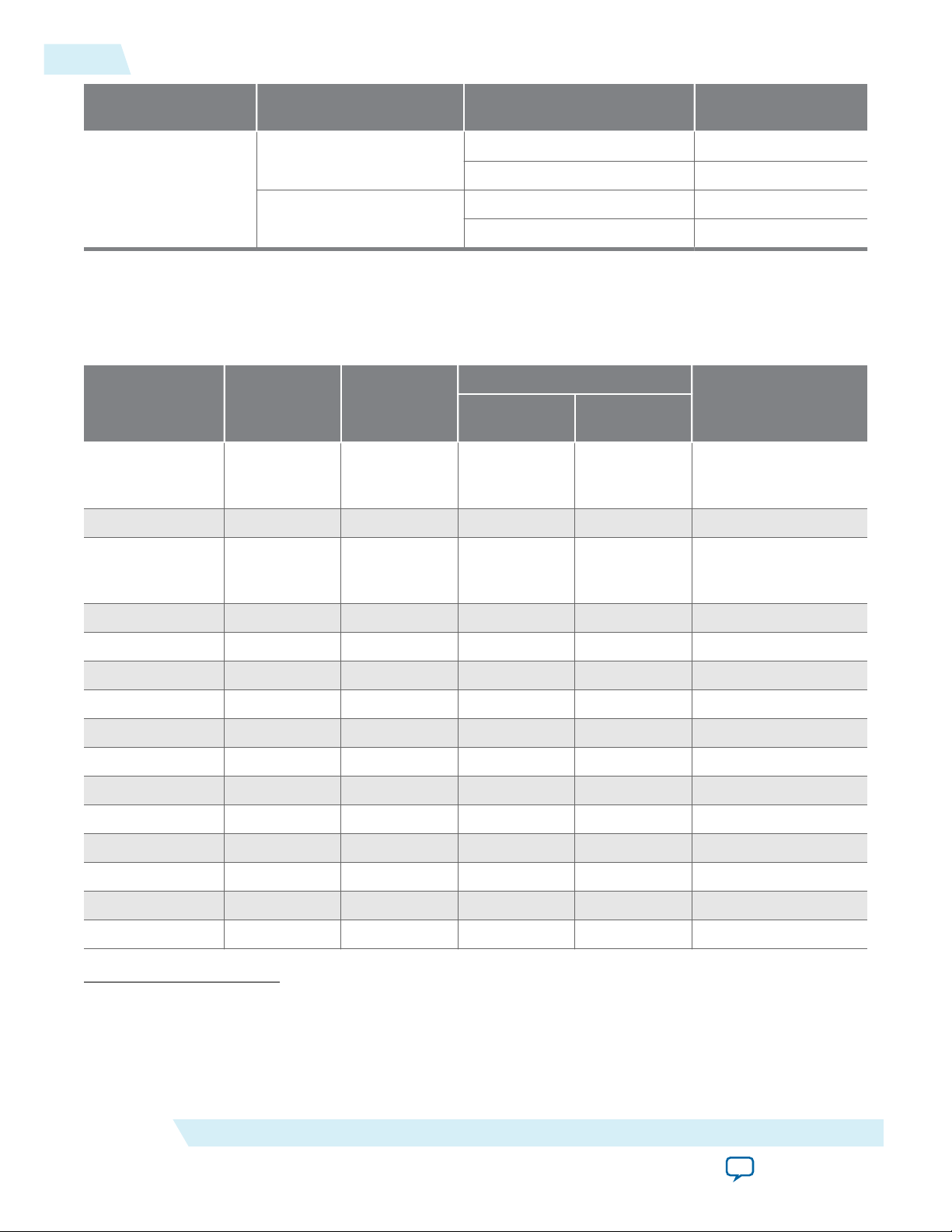
Table 1-1: Brief Information About the JESD204B MegaCore Function
Item Description
Version 15.0
Release Date May 2015
Release
Information
Ordering Code IP-JESD204B
Product ID 0116
Vendor ID 6AF7
• Joint Electron Device Engineering Council (JEDEC)
JESD204B.01, 2012 standard release specification
• Device subclass:
IP Core
Information
Protocol Features
• Subclass 0—Backwards compatible to JESD204A.
• Subclass 1—Uses SYSREF signal to support deterministic
latency.
• Subclass 2—Uses SYNC_N detection to support determin‐
istic latency.
©
2015 Altera Corporation. All rights reserved. ALTERA, ARRIA, CYCLONE, ENPIRION, MAX, MEGACORE, NIOS, QUARTUS and STRATIX words and logos are
trademarks of Altera Corporation and registered in the U.S. Patent and Trademark Office and in other countries. All other words and logos identified as
trademarks or service marks are the property of their respective holders as described at www.altera.com/common/legal.html. Altera warrants performance
of its semiconductor products to current specifications in accordance with Altera's standard warranty, but reserves the right to make changes to any
products and services at any time without notice. Altera assumes no responsibility or liability arising out of the application or use of any information,
product, or service described herein except as expressly agreed to in writing by Altera. Altera customers are advised to obtain the latest version of device
specifications before relying on any published information and before placing orders for products or services.
ISO
9001:2008
Registered
Page 5

1-2
IP Core
Information
JESD204B IP Core Quick Reference
Item Description
Core Features • Run-time configuration of parameters L,M, and F
Typical Application • Wireless communication equipment
UG-01142
2015.05.04
• Data rates up to 12.5 gigabits per second (Gbps)
• Single or multiple lanes (up to 8 lanes per link)
• Serial lane alignment and monitoring
• Lane synchronization
• Modular design that supports multidevice synchronization
• MAC and PHY partitioning
• Deterministic latency support
• 8B/10B encoding
• Scrambling/Descrambling
• Avalon® Streaming (Avalon-ST) interface for transmit and
receive datapaths
• Avalon Memory-Mapped (Avalon-MM) interface for
Configuration and Status registers (CSR)
• Dynamic generation of simulation testbench
• Broadcast equipment
• Military equipment
• Medical equipment
• Test and measurement equipment
Device Family Support • Cyclone® V FPGA device families
• Arria® V FPGA device families
• Arria V GZ FPGA device families
• Arria 10 FPGA device families
• Stratix® V FPGA device families
Refer to the device support table andWhat’s New in Altera IP
page of the Altera website for detailed information.
Design Tools • Qsys parameter editor in the Quartus II software for design
creation and compilation
• TimeQuest timing analyzer in the Quartus II software for
timing analysis
• ModelSim®-Altera, Aldec Riviera-Pro, VCS/VCS MX, and
NCSim software for design simulation or synthesis
Related Information
• Altera Software Installation and Licensing
• What's New in Altera IP
Altera Corporation
JESD204B IP Core Quick Reference
Send Feedback
Page 6

2015.05.04
www.altera.com
101 Innovation Drive, San Jose, CA 95134
About the JESD204B IP Core
2
UG-01142
Subscribe
Send Feedback
The Altera JESD204B IP core is a high-speed point-to-point serial interface for digital-to-analog (DAC) or
analog-to-digital (ADC) converters to transfer data to FPGA devices. This unidirectional serial interface
runs at a maximum data rate of 12.5 Gbps. This protocol offers higher bandwidth, low I/O count and
supports scalability in both number of lanes and data rates. The JESD204B IP core addresses multi-device
synchronization by introducing Subclass 1 and Subclass 2 to achieve deterministic latency.
The JESD204B IP core incorporates:
• Media access control (MAC)—data link layer (DLL) block that controls the link states and character
replacement.
• Physical layer (PHY)—physical coding sublayer (PCS) and physical media attachment (PMA) block.
The JESD204B IP core does not incorporate the Transport Layer (TL) that controls the frame assembly
and disassembly. The TL and test components are provided as part of a design example component where
you can customize the design for different converter devices.
©
2015 Altera Corporation. All rights reserved. ALTERA, ARRIA, CYCLONE, ENPIRION, MAX, MEGACORE, NIOS, QUARTUS and STRATIX words and logos are
trademarks of Altera Corporation and registered in the U.S. Patent and Trademark Office and in other countries. All other words and logos identified as
trademarks or service marks are the property of their respective holders as described at www.altera.com/common/legal.html. Altera warrants performance
of its semiconductor products to current specifications in accordance with Altera's standard warranty, but reserves the right to make changes to any
products and services at any time without notice. Altera assumes no responsibility or liability arising out of the application or use of any information,
product, or service described herein except as expressly agreed to in writing by Altera. Altera customers are advised to obtain the latest version of device
specifications before relying on any published information and before placing orders for products or services.
ISO
9001:2008
Registered
Page 7

JESD204B TX
IP Core
FPGA
M Converters
1 Link, L Lanes
SYNC_N
M Converters
M Converters
SYNC_N
SYNC_N
M Converters
SYNC_N
JESD204B RX
IP Core
1 Link, L Lanes
1 Link, L Lanes
1 Link, L Lanes
DAC Device
Clock 1
ADC Device
Clock 1
Multi-Device
Synchronization
through Subclass 1
or Subclass 2
Multi-Device
Synchronization
through Subclass 1
or Subclass 2
Logic Device (TX)
Device Clock 2
Logic Device (RX)
Device Clock 2
JESD204B TX
IP Core
JESD204B RX
IP Core
2-2
About the JESD204B IP Core
Figure 2-1: Typical System Application for JESD204B IP Core
The JESD204B IP core utilizes the Avalon-ST source and sink interfaces, with unidirectional flow of data,
to transmit and receive data on the FPGA fabric interface.
UG-01142
2015.05.04
Key features of the JESD204B IP core:
• Data rate of up to 12.5 Gbps
• Run-time JESD204B parameter configuration (L, M, F, S, N, K, CS, CF)
• MAC and PHY partitioning for portability
• Subclass 0 mode for backward compatibility to JESD204A
• Subclass 1 mode for deterministic latency support (using SYSREF) between the ADC/DAC and logic
• Subclass 2 mode for deterministic latency support (using SYNC_N) between the ADC/DAC and logic
Altera Corporation
• Multi-device synchronization
device
device
About the JESD204B IP Core
Send Feedback
Page 8

UG-01142
2015.05.04
Datapath Modes
The JESD204B IP core supports TX-only, RX-only, and Duplex (TX and RX) mode. The IP core is a
unidirectional protocol where interfacing to ADC utilizes the transceiver RX path and interfacing to DAC
utilizes the transceiver TX path.
The JESD204B IP core generates a single link with a single lane and up to a maximum of 8 lanes. If there
are two ADC links that need to be synchronized, you have to generate two JESD204B IP cores and then
manage the deterministic latency and synchronization signals, like SYSREF and SYNC_N, at your custom
wrapper level.
The JESD204B IP core supports duplex mode only if the LMF configuration for ADC (RX) is the same as
DAC (TX) and with the same data rate. This use case is mainly for prototyping with internal serial
loopback mode. This is because typically as a unidirectional protocol, the LMF configuration of converter
devices for both DAC and ADC are not identical.
IP Core Variation
The JESD204B IP core has three core variations:
Datapath Modes
2-3
• JESD204B MAC only
• JESD204B PHY only
• JESD204B MAC and PHY
In a subsystem where there are multiple ADC and DAC converters, you need to use the Quartus II
software to merge the transceivers and group them into the transceiver architecture. For example, to
create two instances of the JESD204B TX IP core with four lanes each and four instances of the JESD204
RX IP core with two lanes each, you can apply one of the following options:
• MAC and PHY option
1. Generate JESD204B TX IP core with four lanes and JESD204B RX IP core with two lanes.
2. Instantiate the desired components.
3. Use the Quartus II software to merge the PHY lanes.
• MAC only and PHY only option—based on the configuration above, there are a total of eight lanes in
duplex mode.
1. Generate the JESD204B Duplex PHY with a total of eight lanes. (TX skew is reduced in this
configuration as the channels are bonded).
2. Generate the JESD204B TX MAC with four lanes and instantiate it two times.
3. Generate the JESD204B RX MAC with two lanes and instantiate it four times.
4. Create a wrapper to connect the JESD204B TX MAC and RX MAC with the JESD204B Duplex
PHY.
Note:
If the data rate for TX and RX is different, the transceiver does not allow duplex mode to generate a
duplex PHY. In this case, you have to generate a RX-only PHY on the RX data rate and a TX-only
PHY on the TX data rate.
About the JESD204B IP Core
Send Feedback
Altera Corporation
Page 9

2-4
JESD204B IP Core Configuration
JESD204B IP Core Configuration
Table 2-1: JESD204B IP Core Configuration
Symbol Description Value
L Number of lanes per converter device 1-8
M Number of converters per device 1-256
F Number of octets per frame 1, 2, 4-256
S Number of transmitted samples per converter per frame 1-32
N Number of conversion bits per converter 1-32
UG-01142
2015.05.04
N' Number of transmitted bits per sample (JESD204 word size,
1-32
which is in nibble group)
K Number of frames per multiframe 17/F ≤ K ≤ 32 ; 1-32
CS Number of control bits per conversion sample 0-3
CF Number of control words per frame clock period per link 0-32
HD High Density user data format 0 or 1
LMFC Local multiframe clock (F × K /4) link clock counts
Run-Time Configuration
The JESD204B IP core allows run-time configuration of LMF parameters.
The most critical parameters that must be set correctly during IP generation are the L and F parameters.
Parameter L denotes the maximum lanes supported while parameter F denotes the size of the deskew
buffer needed for deterministic latency. The hardware generates during parameterization, which means
that run-time programmability can only fall back from the parameterized and generated hardware, but
not beyond the parameterized IP core.
You can use run-time configuration for prototyping or evaluating the performance of converter devices
with various LMF configurations. However, in actual production,Altera recommends that you generate
the JESD204B IP core with the intended LMF to get an optimized gate count.
For example, if a converter device supports LMF = 442 and LMF = 222, to check the performance for both
configurations, you need to generate the JESD204B IP core with maximum F and L, which is L = 4 and F
= 2. During operation, you can use the fall back configuration to disable the lanes that are not used in
LMF = 222 mode. You must ensure that other JESD204B configurations like M, N, S, CS, CF, and HD do
not violate the parameter F setting. You can access the Configuration and Status Register (CSR) space to
modify other configurations such as:
(1)
• K (multi-frame)
• device and lane IDs
• enable or disable scrambler
• enable or disable character replacement
(1)
The value of F x K must be divisible by 4.
Altera Corporation
About the JESD204B IP Core
Send Feedback
Page 10

UG-01142
2015.05.04
F Parameter
This parameter indicates how many octets per frame per lane that the JESD204B link is operating in. You
must set the F parameter according to the JESD204B IP Specification for a correct data mapping.
To support the High Density (HD) data format, the JESD204B IP core tracks the start of frame and end of
frame because F can be either an odd or even number. The start of frame and start of multi-frame wrap
around the 32-bits data width architecture. The RX IP core outputs the start of frame (sof[3:0]) and
start of multiframe (somf[3:0]), which act as markers, using the Avalon-ST data stream. Based on these
markers, the transport layer build the frames.
In a simpler system where the HD data format is set to 0, the F will always be 1, 2, 4, 6, 8, and so forth.
This simplifies the transport layer design, so you do not need to use the sof[3:0] and somf[3:0]
markers.
Channel Bonding
The JESD204B IP core supports channel bonding—bonded and non-bonded modes.
The channel bonding mode that you select may contribute to the transmitter channel-to-channel skew. A
bonded transmitter datapath clocking provides low channel-to-channel skew as compared to non-bonded
channel configurations.
Channel Bonding
2-5
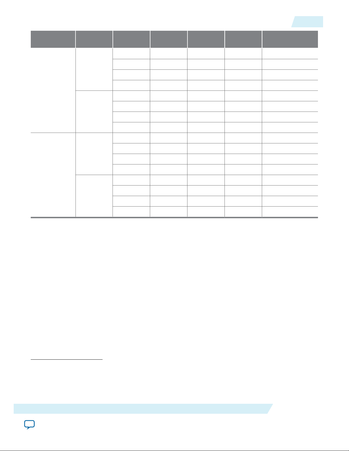
Table 2-2: Maximum Number of Lanes (L) Supported in Bonded and Non-Bonded Mode
• In PHY-only mode, you can generate up to 32 channels, provided that the channels are on the same side. In
MAC and PHY integrated mode, you can generate up to 8 channels.
• In bonded channel configuration, the lower transceiver clock skew and equal latency in the transmitter phase
compensation FIFO for all channels result in a lower channel-to-channel skew. You must use adjacent
channels when you select ×6 bonding. You must also place logical channel 0 in either physical channel 1 or 4.
Physical channels 1 and 4 are indirect drivers of the ×6 clock network. The JESD204B IP core automatically
selects between xN or feedback compensation (fb_compensation) bonding depending on the number of
transceiver channels you set.
• When you select bonded channel and L<6, the IP core automatically selects xN/x6 bonding mode for the
transceiver. When you select bonded channel and L≥6, the IP core automatically selects x6 PLL fb_compensa‐
tion bonding mode for the transceiver
• In non-bonded channel configuration, the transceiver clock skew is higher and latency is unequal in the
transmitter phase compensation FIFO for each channel. This may result in a higher channel-to-channel skew.
Device Family Core Variation Bonding Mode Configuration Maximum Number of
Lanes (L)
PHY only
Bonded 32
Non-bonded 32
(2)
(2)
Arria V
Bonded 6
MAC and PHY
Non-bonded 8
(2)
The maximum lanes listed here is for configuration simplicity. Refer to the Altera Transceiver PHY User
Guide for the actual number of channels supported.
About the JESD204B IP Core
Send Feedback
Altera Corporation
Page 11
2-6
Performance and Resource Utilization
Device Family Core Variation Bonding Mode Configuration Maximum Number of
Bonded 32
Arria V GZ
PHY only
Non-bonded 32
Arria 10
Bonded 8
Stratix V
MAC and PHY
Non-bonded 8
Performance and Resource Utilization
Table 2-3: JESD204B IP Core FPGA Performance
UG-01142
2015.05.04
Lanes (L)
(2)
(2)
Data Rate
Enable Soft PCS
(Gbps)
Link Clock F
(3)
Device Family
PMA Speed
Grade
FPGA Fabric
Speed Grade
Cyclone V 5 <Any
Enable Hard
PCS (Gbps)
1.0 to 5.0 — 125.00
supported
speed grade>
Cyclone V 6 6 or 7 1.0 to 3.125 — 78.125
Arria V <Any
supported
speed grade>
<Any
supported
speed grade>
1.0 to 6.55 —
Arria V GZ 2 3 2.0 to 9.9 —
Arria V GZ 3 4 2.0 to 8.8 —
(4)
(4)
(4)
163.84
247.50
220.00
Arria 10 1 1 2.0 to 12.0 2.0 to 12.5 312.50
Arria 10 2 1 2.0 to 12.0 2.0 to 12.5 312.50
Arria 10 2 2 2.0 to 9.83 2.0 to 12.5 312.50
Arria 10 3 1 2.0 to 12.0 2.0 to 12.5 312.50
Arria 10 3 2 2.0 to 9.83 2.0 to 12.5 —
Arria 10 4 3 2.0 to 8.83 2.0 to 12.5 312.50
MAX
(MHz)
Arria 10 5 3 2.0 to 8.0 2.0 to 8.0 312.50
Stratix V 1 1 or 2 2.0 to 12.2 2.0 to 12.5 312.50
Stratix V 2 1 or 2 2.0 to 12.2 2.0 to 12.5 312.50
Stratix V 2 3 2.0 to 9.8 2.0 to 12.5
(3)
Select Enable Soft PCS to achieve maximum data rate. For the TX IP core, enabling soft PCS incurs an
additional 3–8% increase in resource utilization. For the RX IP core, enabling soft PCS incurs an additional
10–20% increase in resource utilization.
(4)
Enabling Soft PCS does not increase the data rate for the device family and speed grade. You are
recommended to select the Enable Hard PCS option.
Altera Corporation
(5)
312.50
About the JESD204B IP Core
Send Feedback
Page 12

UG-01142
2015.05.04
Performance and Resource Utilization
2-7
Data Rate
Enable Soft PCS
(Gbps)
(3)
Device Family
PMA Speed
Grade
FPGA Fabric
Speed Grade
Enable Hard
PCS (Gbps)
Stratix V 3 1, 2, 3, or 4 2.0 to 8.5 2.0 to 8.5 312.50
The following table lists the resources and expected performance of the JESD204B IP core. These results
are obtained using the Quartus II software targeting the following Altera FPGA devices:
• Cyclone V : 5CGTFD9E5F31I7
• Arria V : 5AGXFB3H4F35C5
• Arria V GZ : 5AGZME5K2F40C3
• Arria 10 : 10AX115H2F34I2SGES
• Stratix V : 5SGXEA7H3F35C3
All the variations for resource utilization are configured with the following parameter settings:
Table 2-4: Parameter Settings To Obtain the Resource Utilization Data
Parameter Setting
JESD204B Wrapper Base and PHY
JESD204B Subclass 1
Data Rate 5 Gbps
Link Clock F
MAX
(MHz)
PCS Option Enabled Hard PCS
PLL Type
• ATX (for 10 series devices)
• CMU (for V series devices)
Bonding Mode Non-bonded
Reference Clock Frequency 125.0 MHz
Octets per frame (F) 1
Enable Scrambler (SCR) Off
Enable Error Code Correction (ECC_EN) Off
(3)
Select Enable Soft PCS to achieve maximum data rate. For the TX IP core, enabling soft PCS incurs an
additional 3–8% increase in resource utilization. For the RX IP core, enabling soft PCS incurs an additional
10–20% increase in resource utilization.
(5)
When using Soft PCS mode at 12.5 Gbps, the timing margin is very limited. You are advised to enable
HIGH fitter effort, register duplication, and register retiming to improve timing performance.
About the JESD204B IP Core
Send Feedback
Altera Corporation
Page 13

2-8
Performance and Resource Utilization
Table 2-5: JESD204B IP Core Resource Utilization
The numbers of ALMs and logic registers in this table are rounded up to the nearest 10.
Note: The resource utilization data are extracted from a full design which includes the Altera Transceiver PHY
Reset Controller IP Core. Thus, the actual resource utilization for the JESD204B IP core should be smaller
by about 15 ALMs and 20 registers.
UG-01142
2015.05.04
Device Family Data Path Number of
Lanes
1 1047 1543 1200 1
2 1594 2325 1825 2
RX
4 2832 4043 3080 4
8 5354 7525 5585 8
Cyclone V
1 728 1148 948 0
2 889 1424 1066 0
TX
4 1218 1941 1293 0
8 1715 2837 1757 0
1 1052 1543 1197 1
2 1586 2325 1823 2
RX
4 2830 4043 3077 4
8 5330 7525 5584 8
Arria V
1 719 1148 947 0
2 887 1424 1062 0
TX
4 1208 1941 1292 0
ALMs ALUTs Logic
Registers
Memory Block
(M10K/M20K)
(6) (7)
Arria V GZ
(6)
M10K for Arria V device, M20K for Arria V GZ, Stratix V and Arria 10 devices.
Altera Corporation
8 1724 2853 1754 0
1 1062 1542 1215 0
2 1634 2363 1858 0
RX
4 2934 4097 3141 0
8 5526 7697 5711 0
1 728 1150 948 0
2 937 1488 1083 0
TX
4 1365 2114 1354 0
8 2141 3417 1895 0
About the JESD204B IP Core
Send Feedback
Page 14
UG-01142
2015.05.04
Performance and Resource Utilization
2-9
Device Family Data Path Number of
Lanes
1 1043 1504 1194 0
2 1575 2265 1815 0
RX
4 2828 3927 3060 0
8 5356 7347 5546 0
Arria 10
1 695 1092 931 0
2 878 1373 1049 0
TX
4 1240 1888 1285 0
8 1908 2969 1757 0
1 1056 1542 1215 0
2 1642 2363 1857 0
RX
4 2936 4097 3140 0
8 5546 7697 5712 0
Stratix V
1 719 1150 948 0
2 937 1488 1083 0
TX
4 1358 2114 1353 0
ALMs ALUTs Logic
Registers
Memory Block
(M10K/M20K)
(6) (7)
8 2137 3417 1894 0
Related Information
• JESD204B IP Core Parameters on page 3-16
• Fitter Resources Reports in the Quartus II Help
Information about the Quartus II resource utilization reporting, including ALMs needed.
(6)
M10K for Arria V device, M20K for Arria V GZ, Stratix V and Arria 10 devices.
(7)
The Quartus II software may auto-fit to use MLAB when the memory size is too small. Conversion from
MLAB to M20K or M10K was performed for the numbers listed above.
(7)
The Quartus II software may auto-fit to use MLAB when the memory size is too small. Conversion from
MLAB to M20K or M10K was performed for the numbers listed above.
About the JESD204B IP Core
Send Feedback
Altera Corporation
Page 15

2015.05.04
www.altera.com
101 Innovation Drive, San Jose, CA 95134
Getting Started
3
UG-01142
Subscribe
Send Feedback
The JESD204B IP core is part of the MegaCore IP Library distributed with the Quartus II software and
downloadable from the Altera website at www.altera.com.
Related Information
Altera Software Installation & Licensing
Introduction to Altera IP Cores
Altera and strategic IP partners offer a broad portfolio of off-the-shelf, configurable IP cores optimized for
Altera devices. The Quartus II software installation includes the Altera IP library. You can integrate
optimized and verified Altera IP cores into your design to shorten design cycles and maximize
performance. You can evaluate any Altera IP core in simulation and compilation in the Quartus II
software. The Quartus II software also supports integration of IP cores from other sources. Use the IP
Catalog to efficiently parameterize and generate synthesis and simulation files for a custom IP variation.
The Altera IP library includes the following categories of IP cores:
• Basic functions
• DSP functions
• Interface protocols
• Low power functions
• Memory interfaces and controllers
• Processors and peripherals
Note:
The IP Catalog (Tools > IP Catalog) and parameter editor replace the MegaWizard™ Plug-In
Manager for IP selection and parameterization, beginning in Quartus II software version 14.0. Use
the IP Catalog and parameter editor to locate and paramaterize Altera and other supported IP
cores.
Related Information
• IP User Guide Documentation
• Altera IP Release Notes
©
2015 Altera Corporation. All rights reserved. ALTERA, ARRIA, CYCLONE, ENPIRION, MAX, MEGACORE, NIOS, QUARTUS and STRATIX words and logos are
trademarks of Altera Corporation and registered in the U.S. Patent and Trademark Office and in other countries. All other words and logos identified as
trademarks or service marks are the property of their respective holders as described at www.altera.com/common/legal.html. Altera warrants performance
of its semiconductor products to current specifications in accordance with Altera's standard warranty, but reserves the right to make changes to any
products and services at any time without notice. Altera assumes no responsibility or liability arising out of the application or use of any information,
product, or service described herein except as expressly agreed to in writing by Altera. Altera customers are advised to obtain the latest version of device
specifications before relying on any published information and before placing orders for products or services.
ISO
9001:2008
Registered
Page 16

acds
quartus - Contains the Quartus II software
ip - Contains the Altera IP Library and third-party IP cores
altera - Contains the Altera IP Library source code
<IP core name> - Contains the IP core source files
3-2
Installing and Licensing IP Cores
Installing and Licensing IP Cores
The Altera IP Library provides many useful IP core functions for your production use without purchasing
an additional license. Some Altera MegaCore IP functions require that you purchase a separate license for
production use. However, the OpenCore® feature allows evaluation of any Altera IP core in simulation
and compilation in the Quartus II software. After you are satisfied with functionality and perfformance,
visit the Self Service Licensing Center to obtain a license number for any Altera product.
Figure 3-1: IP Core Installation Path
Note: The default IP installation directory on Windows is <drive>:\altera\<version number>; on Linux it is
<home directory>/altera/ <version number>.
UG-01142
2015.05.04
Related Information
• Altera Licensing Site
• Altera Software Installation and Licensing Manual
Upgrading IP Cores
IP core variants generated with a previous version of the Quartus II software may require upgrading
before use in the current version of the Quartus II software. Click Project > Upgrade IP Components to
identify and upgrade outdated IP core variants.
Icons in the Upgrade IP Components dialog box indicate when IP upgrade is required, optional, or
unsupported for IP cores in your design. This dialog box may open automatically when you open a
project containing upgradeable IP variations. You must upgrade IP cores that require upgrade before you
can compile the IP variation in the current version of the Quartus II software.
The upgrade process preserves the original IP variation file in the project directory as <my_variant>_
BAK.qsys for IP targeting Arria 10 and later devices, and as <my_variant>_BAK.v, .sv, or .vhd for legacy IP
targeting 28nm devices and greater.
Upgrading IP cores for Arria 10 and later devices may append a unique identifier to the original IP
Note:
core entity name(s), without similarly modifying the IP instance name. There is no requirement to
update these entity references in any supporting Quartus II file; such as the Quartus II Settings File
(.qsf), Synopsys Design Constraints File (.sdc), or SignalTap File (.stp), if these files contain instance
names. The Quartus II software reads only the instance name and ignores the entity name in paths
that specify both names. Use only instance names in assignments.
Altera Corporation
Getting Started
Send Feedback
Page 17
UG-01142
2015.05.04
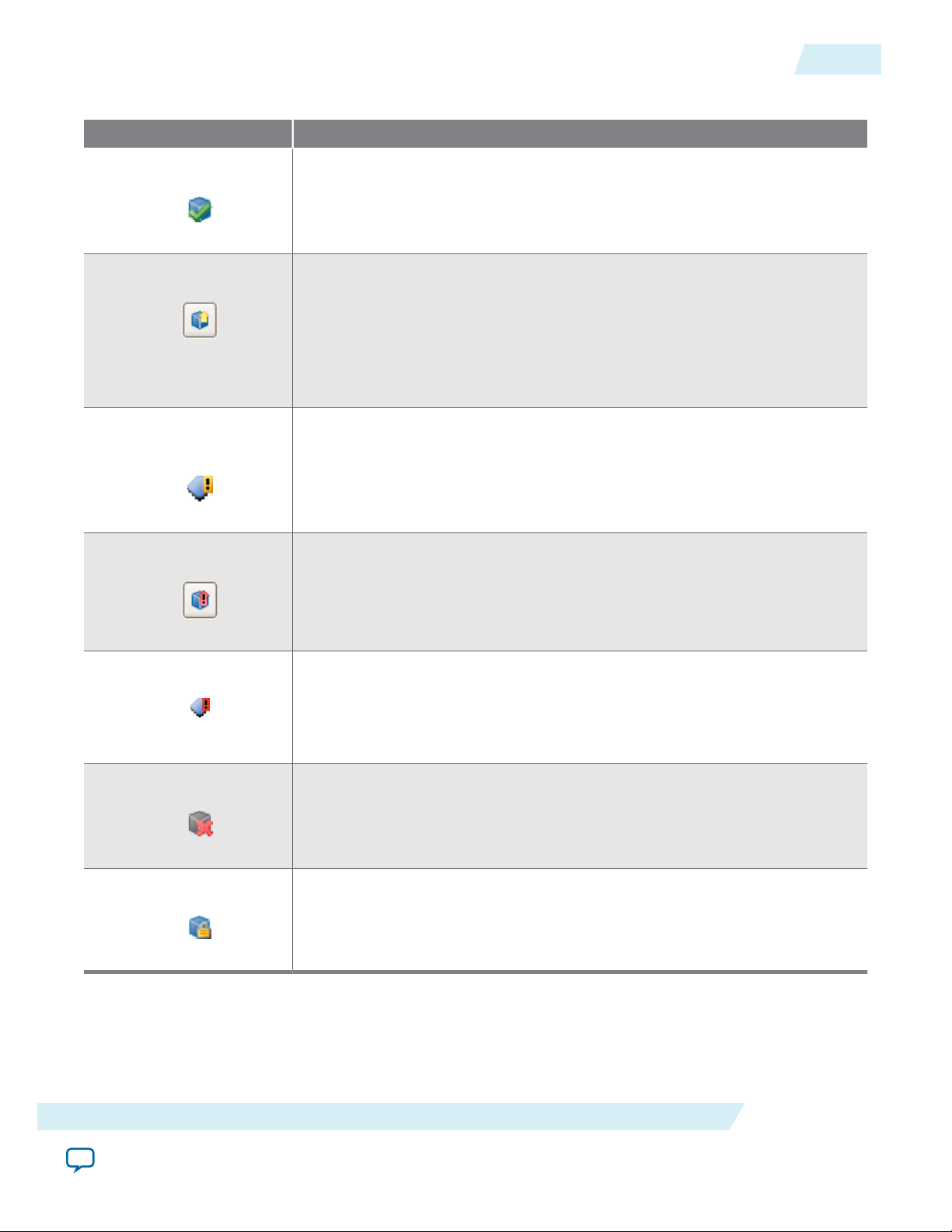
Table 3-1: IP Core Upgrade Status
IP Core Status Description
Upgrading IP Cores
3-3
IP Upgraded
IP Upgrade Optional
IP Upgrade Mismatch
Warning
IP Upgrade Required
Your IP variation uses the lastest version of the IP core.
Upgrade is optional for this IP variation in the current version of the Quartus
II software. You can upgrade this IP variation to take advantage of the latest
development of this IP core. Alternatively you can retain previous IP core
characteristics by declining to upgrade. Refer to the Description for details
about IP core version differences. If you do not upgrade the IP, the IP variation
synthesis and simulation files are unchanged and you cannot modify
parameters until upgrading.
Warning of non-critical IP core differences in migrating IP to another device
family.
You must upgrade the IP variation before compiling in the current version of
the Quartus II software. Refer to the Description for details about IP core
version differences.
IP Upgrade Unspported
Upgrade of the IP variation is not supported in the current version of the
Quartus II software due to incompatibility with the current version of the
Quartus II software. You are prompted to replace the unsupported IP core
with a supported equivalent IP core from the IP Catalog. Refer to the Descrip‐
tion for details about IP core version differences and links to Release Notes.
IP End of Life
Altera designates the IP core as end-of-life status. You may or may not be able
to edit the IP core in the parameter editor. Support for this IP core
discontinues in future releases of the Quartus II software.
Encrypted IP Core
The IP variation is encrypted.
Follow these steps to upgrade IP cores:
1. In the latest version of the Quartus II software, open the Quartus II project containing an outdated IP
core variation. The Upgrade IP Components dialog automatically displays the status of IP cores in
Getting Started
Send Feedback
Altera Corporation
Page 18

Runs “Auto Upgrade” on all supported outdated cores
Opens editor for manual IP upgrade
“Auto Upgrade”
supported
Upgrade required
Upgrade
optional
Upgrade details
“Auto Upgrade”
successful
3-4
Upgrading IP Cores
your project, along with instructions for upgrading each core. Click Project > Upgrade IP
Components to access this dialog box manually.
2. To upgrade one or more IP cores that support automatic upgrade, ensure that the Auto Upgrade
option is turned on for the IP core(s), and then click Perform Automatic Upgrade. The Status and
Version columns update when upgrade is complete. Example designs provided with any Altera IP core
regenerate automatically whenever you upgrade an IP core.
3. To manually upgrade an individual IP core, select the IP core and then click Upgrade in Editor (or
simply double-click the IP core name. The parameter editor opens, allowing you to adjust parameters
and regenerate the latest version of the IP core.
Figure 3-2: Upgrading IP Cores
UG-01142
2015.05.04
Altera Corporation
Note: IP cores older than Quartus II software version 12.0 do not support upgrade. Altera verifies that
the current version of the Quartus II software compiles the previous version of each IP core.
The Altera IP Release Notes reports any verification exceptions for Altera IP cores. Altera does
not verify compilation for IP cores older than the previous two releases.
Related Information
Altera IP Release Notes
Getting Started
Send Feedback
Page 19

UG-01142
2015.05.04
IP Catalog and Parameter Editor
The Quartus II IP Catalog (Tools > IP Catalog) and parameter editor help you easily customize and
integrate IP cores into your project. You can use the IP Catalog and parameter editor to select, customize,
and generate files representing your custom IP variation.
Note: The IP Catalog (Tools > IP Catalog) and parameter editor replace the MegaWizard™ Plug-In
Manager for IP selection and parameterization, beginning in Quartus II software version 14.0. Use
the IP Catalog and parameter editor to locate and paramaterize Altera IP cores.
The IP Catalog lists installed IP cores available for your design. Double-click any IP core to launch the
parameter editor and generate files representing your IP variation. The parameter editor prompts you to
specify an IP variation name, optional ports, and output file generation options. The parameter editor
generates a top-level Qsys system file (.qsys) or Quartus II IP file (.qip) representing the IP core in your
project. You can also parameterize an IP variation without an open project.
Use the following features to help you quickly locate and select an IP core:
• Filter IP Catalog to Show IP for active device family or Show IP for all device families. If you have no
project open, select the Device Family in IP Catalog.
• Type in the Search field to locate any full or partial IP core name in IP Catalog.
• Right-click an IP core name in IP Catalog to display details about supported devices, open the IP core's
installation folder, and view links to documentation.
• Click Search for Partner IP, to access partner IP information on the Altera website.
IP Catalog and Parameter Editor
3-5
Getting Started
Send Feedback
Altera Corporation
Page 20
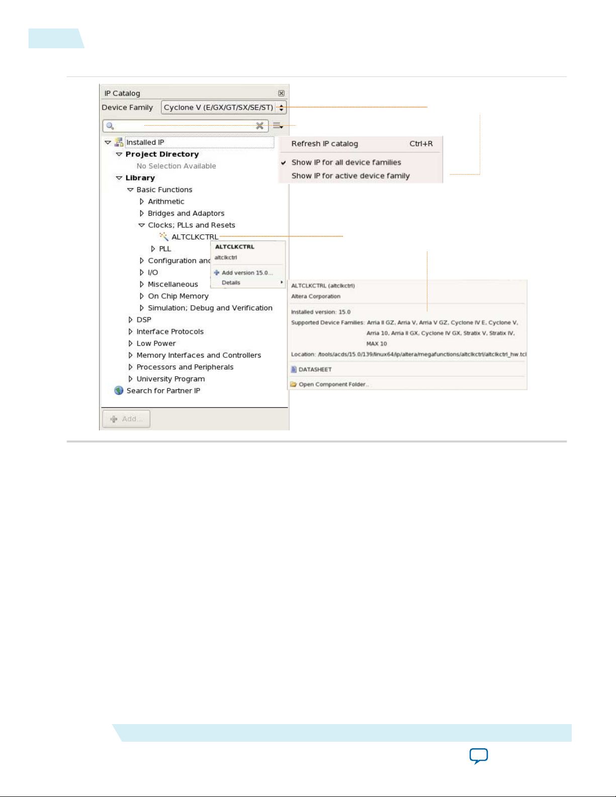
Search for installed IP cores
Double-click to customize, right-click for
detailed information
Show IP only for target device
3-6
Design Walkthrough
Figure 3-3: Quartus II IP Catalog
UG-01142
2015.05.04
Note: The IP Catalog is also available in Qsys (View > IP Catalog). The Qsys IP Catalog includes
exclusive system interconnect, video and image processing, and other system-level IP that are not
available in the Quartus II IP Catalog. For more information about using the Qsys IP Catalog, refer
to Creating a System with Qsys in the Quartus II Handbook.
Design Walkthrough
This walkthrough explains how to create a JESD204B IP core design using Qsys in the Quartus II
software. After you generate a custom variation of the JESD204B IP core, you can incorporate it into your
overall project.
Creating a New Quartus II Project
You can create a new Quartus II project with the New Project Wizard. This process allows you to:
Altera Corporation
Getting Started
Send Feedback
Page 21

UG-01142
2015.05.04
• specify the working directory for the project.
• assign the project name.
• designate the name of the top-level design entity.
1. From the Windows Start menu, select Programs > Altera > Quartus II <version> to launch the
Quartus II software. Alternatively, you can use the Quartus II Web Edition software.
2. On the File menu, click New Project Wizard.
3. In the New Project Wizard: Directory, Name, Top-Level Entity page, specify the working directory,
project name, and top-level design entity name. Click Next.
4. In the New Project Wizard: Add Files page, select the existing design files (if any) you want to include
in the project.
(8)
Click Next.
5. In the New Project Wizard: Family & Device Settings page, select the device family and specific
device you want to target for compilation. Click Next.
6. In the EDA Tool Settings page, select the EDA tools you want to use with the Quartus II software to
develop your project.
7. Review the summary of your chosen settings in the New Project Wizard window, then click Finish to
complete the Quartus II project creation.
Parameterizing and Generating the IP Core
Parameterizing and Generating the IP Core
3-7
Before you begin
Refer to Table 3-6 for the IP core parameter values and description.
1. In the IP Catalog (Tools > IP Catalog), locate and double-click the name of the IP core you want to
customize.
2. Specify a top-level name for your custom IP variation. This name identifies the IP core variation files
in your project. If prompted, also specify the target Altera device family and output file HDL
preference. Click OK.
3. In the Main tab, set the following options:
• Jesd204b wrapper
• Data path
• Jesd204b subclass
• Data Rate
• PCS Option
• PLL Type
• Bonding Mode
• PLL/CDR Reference Clock Frequency
• Enable Bit reversal and Byte reversal
• Enable Transceiver Dynamic Reconfiguration
• Enable Altera Debug Master Endpoint
• Enable Capability Registers
(8)
To include existing files, you must specify the directory path to where you installed the JESD204B IP core.
You must also add the user libraries if you installed the MegaCore IP Library in a different directory from
where you installed the Quartus II software.
Getting Started
Send Feedback
Altera Corporation
Page 22

3-8
Generating and Simulating the IP Core Testbench
UG-01142
2015.05.04
• Set user-defined IP identifier
• Enable Control and Status Registers
• Enable Prbs Soft Accumulators
4. In the Jesd204b Configurations tab, select the following configurations:
• Common configurations (L, M, Enable manual F configuration, F, N, N', S, K)
• Advanced configurations (SCR, CS, CF, HD, ECC_EN, PHADJ, ADJCNT, ADJDIR)
5. In the Configurations and Status Registers tab, set the the following configurations:
• Device ID
• Bank ID
• Lane ID
• Lane checksum
6. After parameterizing the core, click Generate Example Design to create the simulation testbench. Skip
to step 8 if you do not want to generate the design example.
7. Set a name for your <example_design_directory> and click OK to generate supporting files and scripts.
The testbench and scripts are located in the <example_design_directory>/ip_sim folder.
The Generate Example Design option generates supporting files for the following entities:
• IP core for simulation—refer to Generating and Simulating the IP Core Testbench on page 3-8
• IP core design example for simulation—refer to Generating and Simulating the Design Example
on page 5-55
• IP core design example for synthesis—refer to Compiling the JESD204B IP Core Design Example
on page 5-57
8. Click Finish or Generate HDL to generate synthesis and other optional files matching your IP
variation specifications. The parameter editor generates the top-level .qip or .qsys IP variation file and
HDL files for synthesis and simulation.
The top-level IP variation is added to the current Quartus II project. Click Project > Add/Remove
Files in Project to manually add a .qip or .qsys file to a project. Make appropriate pin assignments to
connect ports.
Some parameter options are grayed out if they are not supported in a selected configuration or it is
Note:
a derived parameter.
Generating and Simulating the IP Core Testbench
You can simulate your JESD204B IP core variation by using the provided IP core demonstration
testbench.
To use the JESD204B IP core testbench, follow these steps:
1. Generate the simulation model. Refer to Generating the Testbench Simulation Model on page 3-9.
2. Simulate the testbench using the simulator-specific scripts that you have generated. Refer to
Simulating the IP Core Testbench on page 3-9.
Note:
Some configurations are preset and are not programmable in the JESD204B IP core testbench. For
more details, refer to JESD204B IP Core Testbench on page 3-21 or the README.txt file located
in the <example_design_directory>/ip_sim folder.
Altera Corporation
Getting Started
Send Feedback
Page 23

UG-01142
2015.05.04
Generating the Testbench Simulation Model
To generate the testbench simulation model, execute the generated script (gen_sim_verilog.tcl or
gen_sim_vhdl.tcl) located in the <example_design_directory>/ip_sim folder.
To run the Tcl script using the Quartus II sofware, follow these steps:
1. Launch the Quartus II software.
2. On the View menu, click Utility Windows > Tcl Console.
3.
In the Tcl Console, type cd <example_design_directory>/ip_sim to go to the specified
directory.
4.
Type source gen_sim_verilog.tcl (Verilog) or source gen_sim_vhdl.tcl (VHDL)
to generate the simulation files.
To run the Tcl script using the command line, follow these steps:
1. Obtain the Quartus II software resource.
2.
Type cd <example_design_directory>/ip_sim to go to the specified directory.
3.
Type quartus_sh -t gen_sim_verilog.tcl (Verilog) or quartus_sh -t
gen_sim_vhdl.tcl (VHDL) to generate the simulation files.
Simulating the IP Core Testbench
Generating the Testbench Simulation Model
3-9
The JESD204B IP core simulation supports the following simulators:
• ModelSim-Altera SE/AE
• VCS
• VCS MX
• Cadence
• Aldec Riviera
VHDL is not supported in ModelSim-Altera AE, VCS simulators, and Aldec Riviera (for Arria 10
Note:
devices only).
Table 3-2: Simulation Setup Scripts
This table lists the simulation setup scripts and run scripts.
Simulator File Directory Script
ModelSim®-Altera
SE/AE
<example_design_directory>/ip_sim/testbench/setup_
scripts/mentor
VCS <example_design_directory>/ip_sim/testbench/setup_
scripts/synopsys/vcs
VCS MX <example_design_directory>/ip_sim/testbench/setup_
scripts/synopsys/vcsmx
msim_setup.tcl
vcs_setup.sh
vcsmx_setup.sh
synopsys_sim.setup
Aldec Riviera <example_design_directory>/ip_sim/testbench/setup_
Cadence <example_design_directory>/ip_sim/testbench/setup_
Getting Started
Send Feedback
rivierapro_setup.tcl
scripts/aldec
ncsim_setup.sh
scripts/cadence
Altera Corporation
Page 24

3-10
Compiling the JESD204B IP Core Design
Table 3-3: Simulation Run Scripts
Simulator File Directory Script
UG-01142
2015.05.04
ModelSim-Altera
<example_design_directory>/ip_sim/testbench/mentor run_altera_jesd204_tb.tcl
SE/AE
VCS <example_design_directory>/ip_sim/testbench/synopsys/vcs run_altera_jesd204_tb.sh
VCS MX <example_design_directory>/ip_sim/testbench/synopsys/
vcsmx
run_altera_jesd204_tb.sh
Aldec Riviera <example_design_directory>/ip_sim/testbench/aldec run_altera_jesd204_tb.tcl
Cadence <example_design_directory>/ip_sim/testbench/cadence run_altera_jesd204_tb.sh
To simulate the testbench design using the ModelSim-Altera or Aldec Riviera-PRO simulator, follow
these steps:
1. Launch the ModelSim-Altera or Aldec Riviera-PRO simulator.
2. On the File menu, click Change Directory > Select <example_design_directory>/ip_sim/testbench/
<simulator name>.
3. On the File menu, click Load > Macro file. Select run_altera_jes204_tb.tcl. This file compiles the
design and runs the simulation automatically, providing a pass/fail indication on completion.
To simulate the testbench design using the VCS, VCS MX (in Linux), or Cadence simulator, follow these
steps:
1. Launch the VCS, VCS MX, or Cadence simulator.
2. On the File menu, click Change Directory > Select <example_design_directory>/ip_sim/testbench/
<simulator name>.
3. Run the run_altera_jes204_tb.sh file. This file compiles the design and runs the simulation automati‐
cally, providing a pass/fail indication on completion.
Related Information
Simulating Altera Designs
More information about Altera simulation models.
Compiling the JESD204B IP Core Design
Before you begin
Refer to the JESD204B IP Core Design Considerations on page 3-11 before compiling the JESD204B
IP core design.
To compile your design, click Start Compilation on the Processing menu in the Quartus II software. You
can use the generated .qip file to include relevant files into your project.
Related Information
• JESD204B IP Core Design Considerations on page 3-11
• Quartus II Help
More information about compilation in Quartus II software.
Altera Corporation
Getting Started
Send Feedback
Page 25

UG-01142
2015.05.04
Programming an FPGA Device
After successfully compiling your design, program the targeted Altera device with the Quartus II
Programmer and verify the design in hardware. For instructions on programming the FPGA device, refer
to the Device Programming section in volume 3 of the Quartus II Handbook.
Related Information
Device Programming
JESD204B IP Core Design Considerations
You must be aware of the following conditions when integrating the JESD204B IP core in your design:
• Intergrating the IP core in Qsys
• Pin assignments
• Adding external transceiver PLL
• Timing constraints for the input clock
Integrating the JESD204B IP core in Qsys
You can integrate the JESD204B IP core with other Qsys components within Qsys.
Programming an FPGA Device
3-11
You can connect standard interfaces like clock, reset, Avalon-MM, Avalon-ST, HSSI bonded clock, HSSI
serial clock, and interrupt interfaces within Qsys. However, for conduit interfaces, you are advised to
export all those interfaces and handle them outside of Qsys.
(9)
This is because conduit interfaces are not
part of the standard interfaces. Thus, there is no guarantee on compatibility between different conduit
interfaces.
The Transport Layer provided in this JESD204B IP core design example is not supported in Qsys.
Note:
Therefore, you must export all interfaces that connect to the Transport Layer (for example,
jesd204_tx_link interface) and connect them to a transport layer outside of Qsys.
(9)
You can also connect conduit interfaces within Qsys but you must create adapter components to handle all
the incompatibility issues like incompatible signal type and width.
Getting Started
Send Feedback
Altera Corporation
Page 26
3-12
Pin Assignments
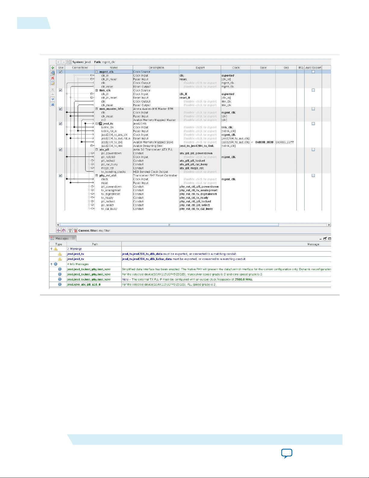
Figure 3-4: Example of Connecting JESD204B IP Core with Other Qsys Components in Qsys
Figure shows an example of how you can connect the IP core with other Qsys components in Qsys.
UG-01142
2015.05.04
Related Information
Transport Layer on page 5-8
Pin Assignments
Set the pin assignments before you compile to provide direction to the Quartus II software Fitter tool. You
must also specify the signals that should be assigned to device I/O pins.
You can create virtual pins to avoid making specific pin assignments for top-level signals. This is useful
when you want to perform compilation, but are not ready to map the design to hardware. Altera
recommends that you create virtual pins for all unused top-level signals to improve timing closure.
Note:
Altera Corporation
Do not create virtual pins for the clock or reset signals.
Getting Started
Send Feedback
Page 27

UG-01142
2015.05.04
Adding External Transceiver PLL
The JESD204B IP core variations that target an Arria 10 FPGA device require external transceiver PLLs
for compilation.
JESD204B IP core variations that target a V-series FPGA device contain transceiver PLLs. Therefore, no
external PLLs are required for compilation.
You are recommend to use an ATX PLL or CMU PLL to get a better jitter performance.
Note: The PMA width is 20 bits for Hard PCS and 40 bits for Soft PCS.
Related Information
Arria 10 Transceiver PHY User Guide
More information about the Arria 10 transceiver PLLs and clock network.
Timing Constraints For Input Clocks
When you generate the JESD204B IP core variation, the Quartus II software generates a Synopsys Design
Constraints File (.sdc) that specifies the timing constraints for the input clocks to your IP core.
When you generate the JESD204B IP core, your design is not yet complete and the JESD204B IP core is
not yet connected in the design. The final clock names and paths are not yet known. Therefore, the
Quartus II software cannot incorporate the final signal names in the .sdc file that it automatically
generates. Instead, you must manually modify the clock signal names in this file to integrate these
constraints with the timing constraints for your full design.
Adding External Transceiver PLL
3-13
This section describes how to integrate the timing constraints that the Quartus II software generates with
your IP core into the timing constraints for your design.
The Quartus II software automatically generates the altera_jesd204.sdc file that contains the JESD204B IP
core's timing constraints.
Three clocks are created at the input clock port:
• JESD204B TX IP core:
• txlink_clk
• reconfig_to_xcvr[0] (for Arria V, Cyclone V, and Stratix V devices only)
• reconfig_clk (for Arria 10 device only)
• tx_avs_clk
• JESD204B RX IP core:
• rxlink_clk
• reconfig_to_xcvr[0] (for Arria V, Cyclone V, and Stratix V devices only)
• reconfig_clk (for Arria 10 device only)
• rx_avs_clk
In a functional system design, these clocks (except for reconfig_to_xcvr[0] clock) are typically
provided by the core PLL.
Getting Started
Send Feedback
Altera Corporation
Page 28

3-14
Timing Constraints For Input Clocks
UG-01142
2015.05.04
In the .sdc file for your project, make the following command changes:
• Specify the PLL clock reference pin frequency using the create_clock command.
• Derive the PLL generated output clocks from the Altera PLL IP Core (for Arria V, Cyclone V and
Stratix V) or Altera I/O PLL IP Core (for Arria 10) using the derive_pll_clocks command.
• Comment out the create_clock commands for the txlink_clk, reconfig_to_xcvr[0] or
reconfig_clk, and tx_avs_clk, rxlink_clk, and rx_avs_clk clocks in the altera_jesd204.sdc file.
• Identify the base and generated clock name that correlates to the txlink_clk, reconfig_clk, and
tx_avs_clk, rxlink_clk, and rx_avs_clk clocks using the report_clock command.
• Describe the relationship between base and generated clocks in the design using the
set_clock_groups command.
After you complete your design, you must modify the clock names in your .sdc file to the full-design clock
names, taking into account both the IP core instance name in the full design, and the design hierarchy. Be
careful when adding the timing exceptions based on your design, for example, when the JESD204B IP
core handles asynchronous timing between the txlink_clk, rxlink_clk, pll_ref_clk, tx_avs_clk,
rx_avs_clk, and reconfig_clk (for Arria 10 only) clocks.
The table below shows an example of clock names in the altera_jesd204.sdc and input clock names in the
user design. In this example, there is a dedicated input clock for the transceiver TX PLL and CDR at the
refclk pin. The device_clk is the input to the core PLL clkin pin. The IP core and transceiver Avalon-
MM interfaces have separate external clock sources with different frequencies.
Altera Corporation
Getting Started
Send Feedback
Page 29

UG-01142
2015.05.04
Table 3-4: Example A
Timing Constraints For Input Clocks
3-15
Original clock
names in altera_
jesd204.sdc
tx_pll_ref_clk
rx_pll_ref_clk
txlink_clk
rxlink_clk
tx_avs_clk
rx_avs_clk
reconfig_clk
(10)
User design input
clock names
xcvr_tx_rx_refclk 250
device_clk 125
jesd204_avs_clk 100
phy_mgmt_clk 75
Frequency
(MHz)
Recommended SDC timing constraint
create_clock -name xcvr_tx_rx_refclk -period 4.0
[get_ports xcvr_tx_rx_refclk ]
create_clock -name device_clk -period 8.0 [get_ports
device_clk]
create_clock -name jesd204_avs_clk -period 10.0
[get_ports jesd204_avs_clk]
create_clock -name phy_mgmt_clk -period 13.3 [get_
ports phy_mgmt_clk]
derive_pll_clocks
set_clock_groups -asynchronous \
-group {xcvr_tx_rx_refclk \
<base and generated clock names as reported by
report_clock commands> \
} \
-group {device_clk \
<base and generated clock names as reported by
report_clock commands> \
} \
-group {jesd204_avs_clk} \
-group {phy_mgmt_clk \
<base and generated clock names as reported by
report_clock commands> \
}
However, if your design requires you to connect the
rx_avs_clk and reconfig_clk to the same clock,
you need to put them in the same clock group.
The table below shows an example where the device_clk in this design is an input into the transceiver
refclk pin. The IP core's Avalon-MM interface shares the same clock source as the transceiver
management clock.
(10)
For Arria 10 device only.
Getting Started
Send Feedback
Altera Corporation
Page 30

3-16
JESD204B IP Core Parameters
Table 3-5: Example B
UG-01142
2015.05.04
Original clock
names in altera_
jesd204.sdc
tx_pll_ref_clk
rx_pll_ref_clk
txlink_clk
rxlink_clk
tx_avs_clk
rx_avs_clk
reconfig_clk
(11)
User design input
clock names
device_clk 125
mgmt_clk 100
Frequency
(MHz)
Recommended SDC timing constraint
create_clock -name device_clk -period 8.0 [get_ports
device_clk]
create_clock -name mgmt_clk -period 10.0 [get_ports
mgmt_clk]
derive_pll_clocks
set_clock_groups -asynchronous \
-group {device_clk \
<base and generated clock names as reported by
report_clock commands> \
} \
-group {mgmt_clk \
<base and generated clock names as reported by
report_clock commands> \
}
JESD204B IP Core Parameters
Table 3-6: JESD204B IP Core Parameters
Parameter Value Description
Main Tab
Device Family
JESD204B Wrapper
(11)
For Arria 10 device only.
• Arria V
• Arria V GZ
• Arria 10
• Cyclone V
• Stratix V
• Base Only
• PHY Only
• Both Base
and PHY
Select the targeted device family.
Select the JESD204B wrapper.
• Base Only—generates the DLL only.
• PHY Only—generates the transceiver PHY layer only (soft
and hard PCS).
• Both Base and PHY—generates both DLL and transceiver
PHY layers.
Altera Corporation
Getting Started
Send Feedback
Page 31

UG-01142
2015.05.04
JESD204B IP Core Parameters
Parameter Value Description
3-17
Data Path
• Receiver
• Transmitter
• Duplex
Select the operation modes. This selection enables or disables
the receiver and transmitter supporting logic.
• RX—instantiates the receiver to interface to the ADC.
• TX—instantiates the transmitter to interface to the DAC.
• Duplex—instantiates the receiver and transmitter to
interface to both the ADC and DAC.
JESD204B Subclass • 0
• 1
• 2
Select the JESD204B subclass modes.
• 0—Set subclass 0
• 1—Set subclass 1
• 2—Set subclass 2
Data Rate 1.0–12.5 Set the data rate for each lane.
• Cyclone V—1.0 Gbps to 5.0 Gbps
• Arria V—1.0 Gbps to 6.55 Gbps
• Arria V GZ—2.0 Gbps to 9.9 Gbps
• Arria 10—2.0 Gbps to 12.5 Gbps
• Stratix V—2.0 Gbps to 12.5 Gbps
PCS Option • Enabled
Hard PCS
• Enabled Soft
PCS
Select the PCS modes.
• Enabled Hard PCS—utilize Hard PCS components. Select
this option to minimize resource utilization with data rate
that supports up to the limitation of the Hard PCS.
(12)
Note: For this setting, you will utilize 8G PCS mode
with 20 bits PMA width and 32 bits PCS width.
• Enabled Soft PCS—utilize Soft PCS components. Select this
option to allow higher supported data rate but increase in
resource utilization.
Note: For this setting, you will utilize 10G PCS mode
with 40 bits PMA width and 40 bits PCS width.
PLL Type • CMU
• ATX
Select the Phase-Locked Loop (PLL) types, depending on the
FPGA device family.
• Cylone V—CMU
• Arria V—CMU
• Stratix V—CMU, ATX
(12)
The maximum data rate is limited by different device speed grade, transceiver PMA speed grade, and
PCS options. Refer to Table 3-4 for the maximum data rate support.
Getting Started
Send Feedback
Altera Corporation
Page 32

3-18
JESD204B IP Core Parameters
Parameter Value Description
UG-01142
2015.05.04
Bonding Mode
PLL/CDR Reference
Clock Frequency
Enable Bit reversal and
Byte reversal
Enable Transceiver
Dynamic Reconfigura‐
tion
Enable Altera Debug
Master Endpoint
(14)
• Bonded
• Non-bonded
Select the bonding modes.
• Bonded—select this option to minimize inter-lanes skew
for the transmitter datapath.
• Non-bonded—select this option to disable inter-lanes skew
control for the transmitter datapath.
Note: The bonding type is automatically selected based on
the device family and number of lanes that you set.
50.0–625.0 Set the transceiver reference clock frequency for PLL or CDR.
On, Off Turn on this option to set the data transmission order in MSB-
first serialization. If this option is off, the data transmission
order is in LSB-first serialization.
On, Off
Turn on this option to enable dynamic data rate change. When
you enable this option, you need to connect the reconfigura‐
tion interface to the transceiver reconfiguration controller.
(13)
For Arria 10 devices, turn on this option to enable the
Transceiver Native PHY reconfiguration interface with "Share
Reconfiguration Interface" enabled for multiple channels.
On, Off Turn on this option for the Transceiver Native PHY IP core to
include an embedded Altera Debug Master Endpoint (ADME).
This ADME connects internally to the Avalon-MM slave
interface of the Transceiver Native PHY and can access the
reconfiguration space of the transceiver. It can perform certain
test and debug functions via JTAG using System Console.
Enable Capability
Registers
Set user-defined IP
identifier
(13)
To perform dynamic reconfiguration, you have to instantiate the Transceiver Reconfiguration Controller
from the IP Catalog and connect it to the JESD204B IP core through the reconfig_to_xcvr and
reconfig_from_xcvr interface.
(14)
To support the Transceiver Toolkit in your design, you must turn on this option.
Altera Corporation
(14)
This parameter is valid only for Arria 10 devices and when you
turn on the Enable Transceiver Dynamic Reconfiguration
parameter.
On, Off Turn on this option to enable capability registers, which
provides high level information about the transceiver channel's
configuration.
0–255 Set a user-defined numeric identifier that can be read from the
user identifer offset when you turn on the Enable Capability
Registers parameter.
Getting Started
Send Feedback
Page 33

UG-01142
2015.05.04
JESD204B IP Core Parameters
Parameter Value Description
3-19
Enable Control and
Status Registers
(14)
On, Off Turn on this option to enable soft registers for reading status
signals and writing control signals on the PHY interface
through the embedded debug. Signals include rx_is_
locktoref, rx_is_locktodata, tx_cal_busy, rx_cal_busy,
rx_serial_loopback, set_rx_locktodata, set_rx_
locktoref, tx_analogreset, tx_digitalreset, rx_
analogreset, and rx_digitalrest. For more information,
refer to the Arria 10 Transceiver User Guide.
Enable Prbs Soft
Accumulators
(14)
On, Off Turn on this option to set the soft logic to perform PRBS bit
and error accumulation when using the hard PRBS generator
and checker.
JESD204B Configurations Tab
Lanes per converter device
1–8 Set the number of lanes per converter device.
(15)
(L)
Converters per device (M) 1–256 Set the number of converters per converter device.
Enable manual F configu‐
ration
On, Off
Turn on this option to set parameter F in manual mode
and enable this parameter to be configurable. Otherwise,
the parameter F is in derived mode.
You have to enable this parameter and configure the
appropriate F value if the transport layer in your design is
supporting Control Word (CF) and/or High Density
format(HD).
Note: The auto derived F value using formula
F=M*S*N\'/(8*L) may not apply if parameter
CF and/or parameter HD are enabled.
Octets per frame (F) 1, 2, 4–256 The number of octets per frame derived from the formula
of F= M*N'*S/(8*L).
Converter resolution (N) 1–32 Set the number of conversion bits per converter.
Transmitted bits per
sample (N')
1–32 Set the number of transmitted bits per sample (JESD204B
word size).
Note: If parameter CF equals to 0 (no control word),
parameter N' must be larger than or equal to
sum of parameter N and parameter CS (N' ≥ N
+ CS). Otherwise, parameter N' must be larger
than or equal to parameter N (N'≥N).
Samples per converter per
frame (S)
(15)
Refer to the Table 3-6 table for the supported range for L.
1–32 Set the number of transmitted samples per converter per
frame.
Getting Started
Send Feedback
Altera Corporation
Page 34

3-20
JESD204B IP Core Parameters
UG-01142
2015.05.04
Frames per multiframe
(K)
1–32 Set the number of frames per multiframe. This value is
dependent on the value of F and is derived using the
following constraints:
• The value of K must fall within the range of 17/F <= K
<= min(32, floor (1024/F))
• The value of F*K must be divisible by 4
Enable scramble (SCR) On, Off Turn on this option to scramble the transmitted data or
descramble the receiving data.
Control Bits (CS) 0–3 Set the number of control bits per conversion sample.
Control Words (CF) 0–32 Set the number of control words per frame clock period
per link.
High density user data
format (HD)
On, Off Turn on this option to set the data format. This parameter
controls whether a sample may be divided over more
lanes.
• On: High Density format
• Off: Data should not cross the lane boundary
Enable Error Code
Correction (ECC_EN)
On, Off Turn on this option to enable error code correction (ECC)
for memory blocks.
Phase adjustment request
(PHADJ)
On, Off Turn on this option to specify the phase adjustment
request to the DAC.
• On: Request for phase adjustment
• Off: No phase adjustment
This parameter is valid for Subclass 2 mode only.
Adjustment resolution
0–15 Set the adjustment resolution for the DAC LMFC.
step count (ADJCNT)
This parameter is valid for Subclass 2 mode only.
Direction of adjustment
(ADJDIR)
• Advance
• Delay
Select to adjust the DAC LMFC direction.
This parameter is valid for Subclass 2 mode only.
Configurations and Status Registers Tab
Device ID 0–255 Set the device ID number.
Bank ID 0–15 Set the device bank ID number.
Lane# ID 0–31 Set the lane ID number.
Lane# checksum 0–255 Set the checksum for each lane ID.
Altera Corporation
Getting Started
Send Feedback
Page 35

UG-01142
2015.05.04
Related Information
Performance and Resource Utilization on page 2-6
JESD204B IP Core Component Files
The following table describes the generated files and other files that may be in your project directory. The
names and types of generated files specified may vary depending on whether you create your design with
VHDL or Verilog HDL.
Table 3-7: Generated Files
Extension Description
<variation name>.v or .vhd IP core variation file, which defines a VHDL or Verilog HDL description of
the custom IP core. Instantiate the entity defined by this file inside of your
design. Include this file when compiling your design in the Quartus II
software.
<variation name>.cmp A VHDL component declaration file for the IP core variation. Add the
contents of this file to any VHDL architecture that instantiates the IP core.
JESD204B IP Core Component Files
3-21
<variation name>.sdc Contains timing constraints for your IP core variation.
<variation name>.qip Contains Quartus II project information for your IP core variation.
<variation name>.tcl Tcl script file to run in Quartus II software.
<variation name>.sip Contains IP core library mapping information required by the Quartus II
software.The Quartus II software generates a . sip file during generation of
some Altera IP cores. You must add any generated .sip file to your project
for use by NativeLink simulation and the Quartus II Archiver.
<variation name>.spd Contains a list of required simulation files for your IP core.
JESD204B IP Core Testbench
The JESD204B IP core includes a testbench to demonstrate a normal link-up sequence for the JESD204B
IP core with a supported configuration. The testbench also provides an example of how to control the
JESD204B IP core interfaces.
The testbench instantiates the JESD204B IP core in duplex mode and connects with the Altera
Transceiver PHY Reset Controller IP core. Some configurations are preset and are not programmable in
the JESD204B IP core testbench. For example, the JESD204B IP core always instantiates in duplex mode
even if RX or TX mode is selected in the JESD204B parameter editor.
Getting Started
Send Feedback
Dynamic reconfiguration is not supported in this JESD204B IP core testbench.
Note:
Altera Corporation
Page 36

Reference Clock
Generator
Link Clock
Generator
AVS Clock
Generator
Packet
Generator
Packet
Checker
ATX PLL
Transceiver PHY Reset Controller
IP Core
JESD204B
IP Core
(Duplex)
Loopback
JESD204B Testbench
3-22
Table 3-8: Preset Configurations for JESD204B IP Core Testbench
JESD204B IP Core Testbench
Configuration Preset Value
JESD204B Wrapper Base and PHY (MAC and PHY)
Data Path Duplex
UG-01142
2015.05.04
PLL/CDR Reference Clock Frequency
Link Clock Data rate/40
AVS Clock 125 MHz
Figure 3-5: JESD204B IP Core Testbench Block Diagram
The external ATX PLL is present only in the JESD204B IP core testbench targeting an Arria 10 FPGA
device family.
• data_rate/20 (if you turn on Enabled Hard PCS)
• data_rate/40 (if you turn on Enabled Soft PCS)
Related Information
Generating and Simulating the IP Core Testbench on page 3-8
Altera Corporation
Getting Started
Send Feedback
Page 37

UG-01142
2015.05.04
Testbench Simulation Flow
The JESD204B testbench simulation flow:
1. At the start, the system is under reset (all the components are in reset).
2. After 100 ns, the Transceiver Reset Controller IP core power up and wait for the tx_ready signal from
the Transceiver Reset Controller IP to assert.
3. The reset signal of the JESD204B TX Avalon-MM interface is released (go HIGH) once the tx_ready
signal is asserted. At the next positive edge of the link_clk signal, the JESD204B TX link powers up by
releasing its reset signal.
4. The JESD204B TX link starts transmitting K28.5 characters and wait for the Transceiver Reset
Controller IP core to assert the rx_ready signal.
5. The reset signal of the JESD204B RX Avalon-MM interface is released (go HIGH) once the rx_ready
signal is asserted. At the next positive edge of the link_clk signal, the JESD204B RX link powers up by
releasing its reset signal.
6. Once the link is out of reset, a SYSREF pulse is generated to reset the LMFC counter inside both the
JESD204B TX and RX IP core.
7. When the txlink_ready signal is asserted, the packet generator starts sending packets to the TX
datapath.
8. The packet checker starts comparing the packet sent from the TX datapath and received at the RX
datapath after the rxlink_valid signal is asserted.
9. The testbench reports a pass or fail when all the packets are received and compared.
Testbench Simulation Flow
3-23
The testbench concludes by checking that all the packets have been received.
If no error is detected, the testbench issues a TESTBENCH PASSED message stating that the simulation
was successful. If an error is detected, the testbench issues a TESTBENCH FAILED message to indicate
that the testbench has failed.
Getting Started
Send Feedback
Altera Corporation
Page 38

2015.05.04
www.altera.com
101 Innovation Drive, San Jose, CA 95134
JESD204B IP Core Functional Description
4
UG-01142
Subscribe
Send Feedback
The JESD204B IP core implements a transmitter (TX) and receiver (RX) block. Each block has two layers
and consists of the following components:
• Media access control (MAC)—DLL block that consists of the link layer (link state machine and
character replacement), CSR, Subclass 1 and 2 deterministic latency, scrambler or descrambler, and
multiframe counter.
• Physical layer (PHY)—PCS and PMA block that consists of the 8B/10B encoder, word aligner,
serializer, and deserializer.
You can specify the datapath and wrapper for your design and generate them separately.
The TX and RX blocks in the DLL utilizes the Avalon-ST interface to transmit or receive data and the
Avalon-MM interface to access the CSRs. The TX and RX blocks operate on 32-bit data width per
channel, where the frame assembly packs the data into four octets per channel. Multiple TX and RX
blocks can share the clock and reset if the link rates are the same.
©
2015 Altera Corporation. All rights reserved. ALTERA, ARRIA, CYCLONE, ENPIRION, MAX, MEGACORE, NIOS, QUARTUS and STRATIX words and logos are
trademarks of Altera Corporation and registered in the U.S. Patent and Trademark Office and in other countries. All other words and logos identified as
trademarks or service marks are the property of their respective holders as described at www.altera.com/common/legal.html. Altera warrants performance
of its semiconductor products to current specifications in accordance with Altera's standard warranty, but reserves the right to make changes to any
products and services at any time without notice. Altera assumes no responsibility or liability arising out of the application or use of any information,
product, or service described herein except as expressly agreed to in writing by Altera. Altera customers are advised to obtain the latest version of device
specifications before relying on any published information and before placing orders for products or services.
ISO
9001:2008
Registered
Page 39

RX
Driver
TX
Driver
Deserializer
Serializer
Frame/Lane
Alignment
Character
Generation
Descrambler
Scrambler
Data Frame
Assembly
Data Frame
Deassembly
SYSREF
Frame Clock
ADC Application
Layer
DAC Application
Layer
Transport Layer Data Link Layer Physical Layer
Word
Aligner
Soft Logic
Hard Logic
JESD204B IP CoreJESD204B
Design Example
jesd204_tx_top
MAC (jesd204_tx_base)
MAC (jesd204_rx_base) PHY (jesd204_rx_phy)
PHY (jesd204_tx_phy)
jesd204_rx_top
8B/10B
Encoder
8B/10B
Decoder
SYNC~
SYNC~
Frame/Lane
Alignment
Character Buffer/
Replace/
Monitor
4-2
JESD204B IP Core Functional Description
Figure 4-1: Overview of the JESD204B IP Core Block Diagram
UG-01142
2015.05.04
Altera Corporation
JESD204B IP Core Functional Description
Send Feedback
Page 40

TX Frame
Assembly
Per Device
TX CSR
Per Device
TX CTL
Per Device
Scrambler
Data Link
Layer (TX)
Soft
PCS
(TX)
Hard PCS
and
Transceiver
JESD204B
(TX) Per Device
CSR
CSR
CSR
32 Bit PCS
Per Channel
Transceiver (Duplex)
Per Device
SYNC_N
SYSREF
TX_INT
TXLINK_CLKTXFRAME_CLK
Avalon-MM
Avalon-ST
To Avalon
Interface
Bus
RX Frame
Deassembly
Per Device
RX CSR
Per Device
RX CTL
Per Device
Descrambler
Data Link
Layer (RX)
Soft
PCS
(RX)
Hard PCS
and
Transceiver
JESD204B
(RX) Per Device
CSR
CSR
CSR
CSR
CSR
32 Bit PCS
Per Channel
32/40
PCS
SYNC_N
SYSREF
RX_INT
RXLINK_CLK
RXFRAME_CLK
Avalon-MM
Avalon-ST
To Avalon
Interface
Bus
JESD204B TX and RX Transport Layer with Base and Transceiver (Design Example)
Avalon-ST
32 Bits per Channel
Serial Interface
(TX_n, TX_p)
Avalon-ST
32 Bits per Channel
Serial Interface
(RX_n, RX_p)
UG-01142
2015.05.04
JESD204B IP Core Functional Description
Figure 4-2: JESD204B IP Core TX and RX Datapath Block Diagram
The JESD204B IP core utilizes the Avalon-ST source and sink interfaces, with unidirectional flow of data,
to transmit and receive data on the FPGA fabric interface.
4-3
32-Bits Architecture
The JESD204B IP core consist of 32-bit internal datapath per lane. This means that JESD204B IP Core
expects the data samples to be assembled into 32-bit data (4 octets) per lane in the transport layer before
sending the data to the Avalon-ST data bus. The JESD204 IP core operates in the link clock domain. The
link clock runs at (data rate/40) because it is operating in 32-bit data bus after 8B/10B encoding.
JESD204B IP Core Functional Description
As the internal datapath of the core is 32-bits, the (F × K) value must be in the order of 4 to align the
multi-frame length on a 32-bit boundary. Apart from this, the deterministic latency counter values such
as LMFC counter, RBD counter, and Subclass 2 adjustment counter will be in link clock count instead of
frame clock count.
Avalon-ST Interface
The JESD204 IP core and transport layer in the design example use the Avalon-ST source and sink
interfaces. There is no backpressure mechanism implemented in this core. The JESD204B IP core expects
continuous stream of data samples from the upstream device.
Send Feedback
Altera Corporation
Page 41

TX Frame
Deassembly
Per Device
TX CSR
Per Device
TX CTL
Per Device
Scrambler
Data Link
Layer (TX)
Soft
PCS
(TX)
Hard PCS
and
Transceiver
JESD204B
(TX) Per Device
CSR
CSR
CSR
32 Bit PCS
Per Channel
Transceiver (TX)
Per Device
SYNC_N
SYSREF
TX_INT
TXLINK_CLKTXFRAME_CLK
Avalon-MM
Avalon-ST
To Avalon
Interface
Bus
JESD204 TX Transport Layer with
Base and Transceiver Design Example
Avalon-ST
32 Bits per Channel
Serial Interface
(TX_n, TX_p)
4-4
Transmitter
Avalon-MM Interface
The Avalon-MM slave interface provides access to internal CSRs. The read and write data width is 32-bits
(DWORD access). The Avalon-MM slave is asynchronous to the txlink_clk, txframe_clk, rxlink_clk,
and rxframe_clk clock domains. You are recommended to release the reset for the CSR configuration
space first. All run-time JESD204B configurations like L, F, M, N, N', CS, CF, and HD should be set before
releasing the reset for link and frame clock domain.
Each write transfer has a writeWaitTime of 0 cycle while a read transfer has a readWaitTime of 1 cycle and
readLatency of 1 cycle.
Related Information
Avalon Interface Specification
More information about the Avalon-ST and Avalon-MM interfaces, including timing diagrams.
Transmitter
The transmitter block, which interfaces to DAC devices, takes one of more digital sample streams and
converts them into one or more serial streams.
The transmitter performs the following functions:
UG-01142
2015.05.04
• Data scrambling
• Frame or lane alignment
• Character generation
• Serial lane monitoring
• 8B/10B encoding
• Data serializer
Figure 4-3: Transmitter Data Path Block Diagram
Altera Corporation
The transmitter block consists of the following modules:
JESD204B IP Core Functional Description
Send Feedback
Page 42

UG-01142
2015.05.04
• TX CSR—manages the configuration and status registers.
• TX_CTL—manages the SYNC_N signal, state machine that controls the data link layer states, LMFC,
and also the deterministic latency throughout the link.
• TX Scrambler and Data Link Layer—takes in 32-bits of data that implements the Initial Lane
Alignment Sequence (ILAS), performs scrambling, lane insertion and frame alignment of characters.
TX Data Link Layer
The JESD204B IP core TX data link layer includes three phases to establish a synchronized link—Code
Group Synchronization (CGS), Initial Lane Synchronization (ILAS), and User Data phase.
TX CGS
The CGS phase is achieved through the following process:
• Upon reset, the converter device (RX) issues a synchronization request by driving SYNC_N low. The
JESD204 TX IP core transmits a stream of /K/ = /K28.5/ symbols. The receiver synchronizes when it
receives four consecutive /K/ symbols.
• For Subclass 0, the RX converter devices deassert SYNC_N signal at the frame boundary. After all
receivers have deactivated their synchronization requests, the JESD204 TX IP core continues to
emit /K/ symbols until the start of the next frame. The core proceeds to transmit ILAS data sequence
or encoded user data if csr_lane_sync_en signal is disabled.
• For Subclass 1 and 2, the RX converter devices deassert SYNC_N signal at the LMFC boundary. After all
receivers deactivate the SYNC_N signal, the JESD204 TX IP core continues to transmit /K/ symbols until
the next LMFC boundary. At the next LMFC boundary, the JESD204B IP core transmits ILAS data
sequence. (There is no programmability to use a later LMFC boundary.)
TX Data Link Layer
4-5
TX ILAS
When lane alignment sequence is enabled through the csr_lane_sync_en register, the ILAS sequence is
transmitted after the CGS phase. The ILAS phase takes up four multi-frames. For Subclass 0 mode, you
can program the CSR (csr_ilas_multiframe) to extend the ILAS phase to a maximum of 256 multiframes before transitioning to the encoded user data phase. The ILAS data is not scrambled regardless of
whether scrambling is enabled or disabled.
The multi-frame has the following structure:
• Each multi-frame starts with a /R/ character (K28.0) and ends with a /A/ character (K28.3)
• The second multi-frame transmits the ILAS configuration data. The multi-frame starts with /R/
character (K28.0), followed by /Q/ character (K28.4), and then followed by the link configuration data,
which consists of 14 octets as illustrated in the table below. It is then padded with dummy data and
ends with /A/ character (K28.3), marking the end of multi-frame.
• Dummy octets are an 8-bit counter and is always reset when it is not in ILAS phase.
• For a configuration of more than four multi-frames, the multi-frame follows the same rule above and
is padded with dummy data in between /R/ character and /A/ character.
JESD204B IP Core Functional Description
Send Feedback
Altera Corporation
Page 43

4-6
TX ILAS
Table 4-1: Link Configuration Data Transmitted in ILAS Phase
UG-01142
2015.05.04
Configura‐
tion Octet
MSB 6 5 4 3 2 1 LSB
Bits
Description
0 DID[7:0] DID = Device ID
1 ADJCNT[3:0] BID[3:0] ADJCNT = Number of adjustment
resolution steps
(16)
BID = Bank ID
2 0 ADJDIRPHADJLID[4:0]
ADJDIR = Direction to adjust DAC
LMFC
(16)
PHADJ = Phase adjustment
request
(16)
LID = Lane ID
3 SCR 0 0 L[4:0]
SCR = Scrambling enabled/disabled
L = Number of lanes per device
(link)
4 F[7:0] F = Number of octets per frame per
lane
5 0 0 0 K[4:0] K = Number of frames per multi-
frame
6 M[7:0] M = Number of converters per
device
7 CS[1:0] 0 N[4:0]
CS = Number of control bits per
sample
N = Converter resolution
8 SUBCLASSV[2:0] N_PRIME[4:0]
SUBCLASSV = Subclass version
N_PRIME = Total bits per sample
9 JESDV[2:0] S[4:0]
JESDV = JESD204 version
S = Number of samples per
converter per frame
10 HD 0 0 CF[4:0]
HD = High Density data format
CF = Number of control words per
frame clock per link
(16)
Applies to Subclass 2 only.
Altera Corporation
JESD204B IP Core Functional Description
Send Feedback
Page 44

UG-01142
2015.05.04
User Data Phase
4-7
Configura‐
tion Octet
MSB 6 5 4 3 2 1 LSB
Bits
Description
11 RES1[7:0] RES1 = Reserved. Set to 8'h00
12 RES2[7:0] RES2 = Reserved. Set to 8'h00
13 FCHK[7:0]; automatically calculated using run-time
configuration.
FCHK is the modulus 256 of the
sum of the 13 configuration octets
above.
If you change any of the octets
during run-time, make sure to
update the new FCHK value in the
register.
The JESD204 TX IP core also supports debug feature to continuously stay in ILAS phase without exiting.
You can enable this feature by setting the bit in csr_ilas_loop register. There are two modes of entry:
• RX asserts SYNC_N and deasserts it after CGS phase. This activity triggers the ILAS phase and the CSR
will stay in ILAS phase indefinitely until this setting changes.
• Link reinitialization through CSR is initiated. The JESD204B IP core transmits /K/ character and
causes the RX converter to enter CGS phase. After RX deasserts SYNC_N, the CSR enters ILAS phase
and will stay in that phase indefinitely until this setting changes.
In ILAS loop, the multi-frame transmission is the same where /R/ character (K28.0) marks the start of
multi-frame and /A/ character (K28.3) marks the end of multi-frame, with dummy data in between. The
dummy data is an increment of Dx.y.
User Data Phase
During the user data phase, character replacement at the end of frame and end of multi-frame is
opportunistically inserted so that there is no additional overhead for data bandwidth.
Character replacement for non-scrambled data
The character replacement for non-scrambled mode in the IP core follows these JESD204B specification
rules:
• At end of frame (not coinciding with end of multi-frame), which equals the last octet in the previous
frame, the transmitter replaces the octet with /F/ character (K28.7). However, if an alignment character
was transmitted in the previous frame, the original octet will be encoded.
• At the end of a multi-frame, which equals to the last octet in the previous frame, the transmitter
replaces the octet with /A/ character (K28.3), even if a control character was already transmitted in the
previous frame.
For devices that do not support lane synchronization, only /F/ character replacement is done. At every
end of frame, regardless of whether the end of multi-frame equals to the last octet in previous frame, the
transmitter encodes the octet as /F/ character (K28.7) if it fits the rules above.
JESD204B IP Core Functional Description
Send Feedback
Altera Corporation
Page 45

4-8
TX PHY Layer
Character replacement for scrambled data
The character replacement for scrambled data in the IP core follows these JESD204B specification rules:
• At end of frame (not coinciding with end of multi-frame), which equals to 0xFC (D28.7), the
transmitter encodes the octet as /F/ character (K28.7).
• At end of multi-frame, which equals to 0x7C, the transmitter replaces the current last octet as /A/
character (K28.3).
For devices that do not support lane synchronization, only /F/ character replacement is done. At every
end of frame, regardless of whether the end of multi-frame equals to 0xFC (D28.7), the transmitter
encodes the octet as /F/ character (K28.7) if it fits the rules above.
TX PHY Layer
The 8B/10B encoder encodes the data before transmitting them through the serial line. The 8B/10B
encoding has sufficient bit transition density (3-8 transitions per 10-bit symbol) to allow clock recovery by
the receiver. The control characters in this scheme allow the receiver to:
• synchronize to 10-bit boundary.
• insert special character to mark the start and end of frames and start and end of multi-frames.
• detect single bit errors.
UG-01142
2015.05.04
The JESD204 IP core supports transmission order from MSB first as well as LSB first. For MSB first
transmission, the serialization of the left-most bit of 8B/10B code group (bit "a") is transmitted first.
Receiver
The receiver block, which interfaces to ADC devices, receives the serial streams from one or more TX
blocks and converts the streams into one or more sample streams.
The receiver performs the following functions:
• Data deserializer
• 8B/10B decoding
• Lane alignment
• Character replacement
• Data descrambling
Altera Corporation
JESD204B IP Core Functional Description
Send Feedback
Page 46

Transceiver (RX)
Per Device
RX Frame
Deassembly
Per Device
RX CSR
Per Device
RX CTL
Per Device
Descrambler
Data Link
Layer (RX)
Soft
PCS
(RX)
Hard PCS
and
Transceiver
JESD204B
(RX) Per Device
CSR
CSR
CSR
32 Bit PCS
Per Channel
32/40
PCS
SYNC_N
SYSREF
RX_INT
RXLINK_CLK
RXFRAME_CLK
Avalon-MM
Avalon-ST
To Avalon
Interface
Bus
JESD204 RX Transport Layer with
Base and Transceiver Design Example
Avalon-ST
32 Bits per Channel
Serial Interface
(RX_n, RX_p)
UG-01142
2015.05.04
RX Data Link Layer
Figure 4-4: Receiver Data Path Block Diagram
The receiver block includes the following modules:
• RX CSR—manages the configuration and status registers.
• RX_CTL—manages the SYNC_N signal, state machine that controls the data link layer states, LMFC,
and also the buffer release, which is crucial for deterministic latency throughout the link.
• RX Scrambler and Data Link Layer—takes in 32-bits of data that decodes the ILAS, performs descram‐
bling, character replacement as per the JESD204B specification, and error detection (code group error,
frame and lane realignment error).
4-9
RX Data Link Layer
The JESD204B IP core RX data link layer buffers incoming user data on all lanes until the RX elastic
buffers can be released. Special character substitution are done in the TX link so that the RX link can
execute frame and lane alignment monitoring based on the JESD204B specification.
RX CGS
The CGS phase is the link up phase that monitors the detection of /K28.5/ character.
The CGS phase is achieved through the following process:
• Once the word boundary is aligned, the RX PHY layer detects the /K28.5/ 20-bit boundary and
indicate that the character is valid.
• The receiver deasserts SYNC_N on the next frame boundary (for Subclass 0) or on the next LMFC
boundary (for Subclass 1 and 2) after the reception of four successive /K/ characters.
• After correct reception of another four 8B/10B characters, the receiver assumes full code group
synchronization. Error detected in this state machine is the code group error. Code group error always
trigger link reinitialization through the assertion of SYNC_N signal and this cannot be disabled through
the CSR. The CS state machine is defined as CS_INIT, CS_CHECK, and CS_DATA.
• The minimum duration for a synchronization request on the SYNC_N is five frames plus nine octets.
Frame Synchronization
After CGS phase, the receiver assumes that the first non-/K28.5/ character marks the start of frame and
multi-frame. If the transmitter emits an initial lane alignment sequence, the first non-/K28.5/ character
JESD204B IP Core Functional Description
Send Feedback
Altera Corporation
Page 47

4-10
Frame Alignment
will be /K28.0/. Similar to the JESD204 TX IP core, the csr_lane_sync_en is set to 1 by default, thus the
RX core detects the /K/ character to /R/ character transition. If the csr_lane_sync_en is set to 0, the RX
core detects the /K/ character to the first data transition. An ILAS error and unexpected /K/ character is
flagged if either one of these conditions are violated.
When csr_lane_sync_en is set to 0, you have to disable data checking for the first 16 octets of data as the
character replacement block takes 16 octets to recover the end-of-frame pointer for character replace‐
ment. When csr_lane_sync_en is set to 1 (default JESD204B setting), the number of octets to be
discarded depends on the scrambler or descrambler block.
The receiver assumes that a new frame starts in every F octets. The octet counter is used for frame
alignment and lane alignment.
Related Information
• Scrambler/Descrambler on page 4-14
Frame Alignment
The frame alignment is monitored through the alignment character /F/. The transmitter inserts this
character at the end of frame. The /A/ character indicates the end of multi-frame. The character replace‐
ment algorithm depends on whether scrambling is enabled or disabled, regardless of the
csr_lane_sync_en register setting.
UG-01142
2015.05.04
The alignment detection process:
• If two successive valid alignment characters are detected in the same position other than the assumed
end of frame—without receiving a valid or invalid alignment character at the expected position
between two alignment characters—the receiver realigns its frame to the new position of the received
alignment characters.
• If lane realignment can result in frame alignment error, the receiver issues an error.
In the JESD204 RX IP core, the same flexible buffer is used for frame and lane alignment. Lane realign‐
ment gives a correct frame alignment because lane alignment character doubles as a frame alignment
character. A frame realignment can cause an incorrect lane alignment or link latency. The course of action
is for the RX to request for reinitialization through SYNC_N.
Lane Alignment
After the frame synchronization phase has entered FS_DATA, the lane alignment is monitored via /A/
character (/K28.3/) at the end of multi-frame. The first /A/ detection in the ILAS phase is important for
the RX core to determine the minimum RX buffer release for inter-lane alignment. There are two types of
error that is detected in lane alignment phase:
• Arrival of /A/ character from multiple lanes exceed one multi-frame.
• Misalignment detected during user data phase.
(17)
(17)
Dynamic frame realignment and correction is not supported.
Altera Corporation
JESD204B IP Core Functional Description
Send Feedback
Page 48

UG-01142
2015.05.04
ILAS Data
ILAS Data
4-11
The realignment rules for lane alignment are similar to frame alignment:
• If two successive and valid /A/ characters are detected at the same position other than the assumed end
of multi-frame—without receiving a valid/invalid /A/ character at the expected position between
two /A/ characters—the receiver aligns the lane to the position of the newly received /A/ characters.
• If a recent frame alignment causes the loss of lane alignment, the receiver realigns the lane frame—
which is already at the position of the first received /A/ character—at the unexpected position.
The JESD204 RX IP core captures 14 octets of link configuration data that are transmitted on the 2
multi-frame of the ILAS phase. The receiver waits for the reception of /Q/ character that marks the start of
link configuration data and then latch it into ILAS octets, which are per lane basis. You can read the 14
octets captured in the link configuration data through the CSR. You need to first set the
csr_ilas_data_sel register to select which link configuration data lane it is trying to read from. Then,
proceed to read from the csr_ilas_octet register.
Initial Lane Synchronization
The receivers in Subclass 1 and Subclass 2 modes store data in a memory buffer (Subclass 0 mode does not
store data in the buffer but immediately releases them on the frame boundary as soon as the latest lane
arrives.). The RX IP core detects the start of multi-frame of user data per lane and then wait for the latest
lane data to arrive. The latest data is reported as RBD count (csr_rbd_count) value which you can read
from the status register. This is the earliest release opportunity of the data from the deskew FIFO (referred
to as RBD offset).
The JESD204 RX IP core supports RBD release at 0 offset and also provides programmable offset through
RBD count. By default, the RBD release can be programmed through the csr_rbd_offset to release at
the LMFC boundary. If you want to implement an early release mechanism, program it in the
csr_rbd_offset register. The csr_rbd_offset and csr_rbd_count is a counter based on the link clock
boundary (not frame clock boundary). Therefore, the RBD release opportunity is at every four octets.
nd
JESD204B IP Core Functional Description
Send Feedback
Altera Corporation
Page 49

K K K K K K K K K K K K K K K K K K K K K K K K
KKR D D
D D A R Q C C D D D A
L Transmit Lanes
SYSREF
SYNC_N
LMFC
Deterministic Delay from SYSREF
Sampled High to LMFC Zero-Crossing
TX ILA Begins on First LMFC Zero-Crossing
after SYNC_N Is Deasserted
Multi-Frame
TX
Device
K K K K K K K K K K K K
K R D D D D A R Q C C D D D A R D D
Earliest Arrival Lane
SYSREF
SYNC_N
LMFC
Deterministic Delay from
SYSREF Sampled High
to LMFC Zero-Crossing
RX Elastic Buffers Released
RX
Device
K K
K K K K K K K K
K K K K K R D D D D A R Q C C D D D A R D DK K
K K K K K K
K K K K K K K R D D D D A R Q C C D D D A R D DK K
K K K K
K K K K K K K KK K K K
K K K K K K K KK K K K
K KK K K K
K K K K K K KK KK K K
Latest Arrival Lane
Aligned Output on All Lanes
RX Elastic Buffer
Release Opportunity
RBD Frame
Cycles
SYNC_N Deasserted Directly after LMFC Zero Crossing
RBD Frame
Cycles
RBD Frame
Cycles
RBD Frame
Cycles
2 Character Elastic Buffer Delay for Latest Arrival
6 Character Elastic Buffer Delay for Latest Arrival
Deterministic Delay
from TX ILA Output
to RX ILA Output
4-12
RX PHY Layer
Figure 4-5: Subclass 1 Deterministic Latency and Support for Programmable Release Opportunity
UG-01142
2015.05.04
RX PHY Layer
Altera Corporation
The word aligner block identifies the MSB and LSB boundaries of the 10-bit character from the serial bit
stream. Manual alignment is set because the /K/ character must be detected in either LSB first or MSB first
mode. When the programmed word alignment pattern is detected in the current word boundary, the PCS
indicates a valid pattern in the rx_sync_status (mapped as pcs_valid to the IP core). The code
synchronization state is detected after the detection of the /K/ character boundary for all lanes.
In a normal operation, whenever synchronization is lost, JESD204 RX IP core always return back to the
CS_INIT state where the word alignment is initiated. For debug purposes, you can bypass this alignment
by setting the csr_patternalign_en register to 0.
The 8B/10B decoder decode the data after receiving the data through the serial line. The JESD204 IP core
supports transmission order from MSB first as well as LSB first.
The PHY layer can detect 8B/10B not-in-table (NIT) error and also running disparity error.
JESD204B IP Core Functional Description
Send Feedback
Page 50

UG-01142
2015.05.04
Operation
Operating Modes
The JESD204B IP core supports Subclass 0, 1, and 2 operating modes.
Subclass 0
The JESD204 IP core maintains a LMFC counter that counts from 0 to (F × K/4)–1 and wraps around
again. The LMFC counter starts counting at the deassertion of SYNC_N signal from multiple DACs after
synchronization. This is to align the LMFC counter upon transmission and can only be done after all the
converter devices have deasserted its synchronization request signal.
Subclass 1
The JESD204 IP core maintains a LMFC counter that counts from 0 to (F × K/4)–1 and wraps around
again. The LMFC counter will reset within two link clock cycles after converter devices issue a common
SYSREF frequency to all the transmitters and receivers. The SYSREF frequency must be the same for
converter devices that are grouped and synchronized together.
Table 4-2: Example of SYSREF Frequency Calculation
Operation
4-13
In this example, you can choose to perform one of the following options:
• provide two SYSREF and device clock, where the ADC groups share both the device clock and SYSREF (18.75
MHz and 9.375 MHz)
• provide one SYSREF (running at 9.375 MHz) and device clock for all the ADC and DAC groups because the
SYSREF period in the DAC is a multiplication of n integer.
Group Configuration SYSREF Frequency
ADC Group 1 (2 ADCs)
• LMF = 222
(6 GHz / 40) / (2 x 16 / 4) = 18.75 MHz
• K = 16
• Data rate = 6 Gbps
ADC Group 2 (2 ADCs)
• LMF = 811
(6 GHz / 40) / (1 x 32 / 4) = 18.75 MHz
• K = 32
• Data rate = 6 Gbps
DAC Group 3 (2 DACs)
• LMF = 222
(3 GHz / 40) / (2 x 16 / 4) = 9.375 MHz
• K = 16
• Data rate = 3 Gbps
Subclass 2
The JESD204 IP core maintains a LMFC counter that counts from 0 to (F × K/4)–1 and wraps around
again. The LMFC count starts upon reset and the logic device always acts as the timing master. The
converters adjust their own internal LMFC to match the master's counter. The alignment of LMFC within
the system relies on the correct alignment of SYNC_N signal deassertion at the LMFC boundary.
The alignment of LMFC to RX logic is handled within the TX converter. The RX logic releases SYNC_N at
the LMFC tick and the TX converter adjust its internal LMFC to match the RX LMFC.
JESD204B IP Core Functional Description
Send Feedback
Altera Corporation
Page 51

4-14
Scrambler/Descrambler
For the alignment of LMFC to the TX logic, the JESD204 TX IP core samples SYNC_N from the DAC
receiver and reports the relative phase difference between the DAC and TX logic device LMFC in the TX
CSR (dbg_phadj, dbg_adjdir, and dbg_adjcnt). Based on the reported value, you can calculate the
adjustment required. Then, to initiate the link reinitialization through the CSR, set the value in the TX
CSR (csr_phadj, csr_adjdir, and csr_adjcnt). The values on the phase adjustment are embedded in
bytes 1 and 2 of the ILAS sequence that is sent to the DAC during link initialization. On the reception of
the ILAS, the DAC adjusts its LMFC phase by step count value and sends back an error report with the
new LMFC phase information. This process may be repeated until the LMFC at the DAC and the logic
device are aligned.
Scrambler/Descrambler
Both the scrambler and descrambler are designed in a 32-bit parallel implementation and the scrambling/
descrambling order starts from first octet with MSB first.
The JESD204 TX and RX IP core support scrambling by implementing a 32-bit parallel scrambler in each
lane. The scrambler and descrambler are located in the JESD204 IP MAC interfacing to the Avalon-ST
interface. You can enable or disable scrambling and this option applies to all lanes. Mixed mode
operation, where scrambling is enabled for some lanes, is not permitted.
The scrambling polynomial:
1 + x14 + x
15
UG-01142
2015.05.04
The descrambler can self-synchronize in eight octets. In a typical application where the reset value of the
scrambler seed is different from the converter device to FPGA logic device, the correct user data is
recovered in the receiver in two link clocks (due to the 32-bit architecture). The PRBS pattern checker on
the transport layer should always disable checking of the first eight octets from the JESD204 RX IP core.
SYNC_N Signal
For Subclass 0 implementation, the SYNC_N signal from the DAC converters in the same group path must
be combined.
In some applications, multiple converters are grouped together in the same group path to sample a signal
(referred as multipoint link). The FPGA can only start the LMFC counter and its transition to ILAS after
all the links deassert the synchronization request. The JESD204B TX IP core provides three signals to
facilitate this application. The SYNC_N is the direct signal from the DAC converters. The error signaling
from SYNC_N is filtered and sent out as dev_sync_n signal. For Subclass 0, you need to multiplex all the
dev_sync_n signals in the same multipoint link and then input them to the IP core through mdev_sync_n
signal.
Altera Corporation
JESD204B IP Core Functional Description
Send Feedback
Page 52

SYSREF Tied to
0 for Subclass 0
JESD204B IP Core
TX
SYSREF
SYNC_N
DEV_SYNC_N
MDEV_SYNC_N
SYSREF
SYNC_N
DEV_SYNC_N
MDEV_SYNC_N
SYSREF
SYNC_N
DEV_SYNC_N
MDEV_SYNC_N
FPGA Device
Converter Device 0
L
Converter Device 1
L
Converter Device 2
L
SYNC_N
SYNC_N
SYNC_N
Clock Chip
FPGA Reference Clock
SYNC* (1)
DAC Reference
Clock
Note:
1. SYNC* is not associated to SYNC_N in the JESD204B specification. SYNC* refers to JESD204A (Subclass 0) converter devices that
may support synchronization via additional SYNC signalling.
JESD204B IP Core
TX
JESD204B IP Core
TX
UG-01142
2015.05.04
Figure 4-6: Subclass 0 — Combining the SYNC_N Signal for JESD204B TX IP Core
SYNC_N Signal
4-15
For Subclass 1 implementation, you may choose to combine or not to combine the SYNC_N signal from the
converter device. If you implement two ADC converter devices as a multipoint link and one of the
converter is unable to link up, the functional link will still operate. You must manage the trace length for
the SYSREF signal and also the differential pair to minimize skew.
The SYNC_N is the direct signal from the DAC converters. The error signaling from SYNC_N is filtered and
sent out as dev_sync_n output signal. The dev_sync_n signal from the JESD204B TX IP core must
loopback into the mdev_sync_n signal of the same instance without combining the SYNC_N signal.
Apart from that, you must set the same RBD offset value (csr_rbd_offset) to all the JESD204B RX IP
cores within the same multipoint link for the RBD release (the latest lane arrival for each of the links). The
JESD204 RX IP core will deskew and output the data when the RBD offset value is met. The total latency
is consistent in the system and is also the same across multiple resets. Setting a different RBD offset to
each link or setting an early release does not guarantee deterministic latency and data alignment.
JESD204B IP Core Functional Description
Send Feedback
Altera Corporation
Page 53

SYSREF (Subclass 1)
SYSREF
SYNC_N
DEV_SYNC_N
MDEV_SYNC_N
SYSREF
SYNC_N
DEV_SYNC_N
MDEV_SYNC_N
SYSREF
SYNC_N
DEV_SYNC_N
MDEV_SYNC_N
FPGA Device
Converter Device 0
L
Converter Device 1
L
Converter Device 2
L
SYNC_N
SYNC_N
SYNC_N
Clock Chip
and SYSREF
FPGA Reference Clock
SYSREF
DAC Reference
Clock
SYSREF
JESD204B IP Core
TX
JESD204B IP Core
TX
JESD204B IP Core
TX
4-16
Link Reinitialization
Figure 4-7: Subclass 1 — Combining the SYNC_N Signal for JESD204B TX IP Core
UG-01142
2015.05.04
Link Reinitialization
Altera Corporation
Related Information
Programmable RBD Offset on page 6-2
The JESD204B TX and RX IP core support link reinitialization.
JESD204B IP Core Functional Description
Send Feedback
Page 54

UG-01142
2015.05.04
Link Startup Sequence
4-17
There are two modes of entry for link reinitialization:
• Hardware initiated link reinitialization:
• For TX, the reception of SYNC_N for more than five frames and nine octets triggers link reinitializa‐
tion.
• For RX, the loss of code group synchronization, frame alignment and lane alignment errors cause
the IP core to assert SYNC_N and request for link reinitialization.
• Software initiated link reinitialization—both the TX and RX IP core allow software to request for link
reinitialization.
• For TX, the IP core transmits /K/ character and wait for the receiver to assert SYNC_N to indicate
that it has entered CS_INIT state.
• For RX, the IP core asserts SYNC_N to request for link reinitialization.
Hardware initiated link reinitialization can be globally disabled through the csr_link_reinit_disable
register for debug purposes.
Hardware initiated link reinitialization can be issued as interrupt depending on the error type and
interrupt error enable. If lane misalignment has been detected as a result of a phase change in local timing
reference, the software can rely on this interrupt trigger to initiates a LMFC realignment. The realignment
process occurs by first resampling SYSREF and then issuing a link reinitialization request.
Link Startup Sequence
Set the run-time LMF configuration when the txlink_rst_n or rxlink_rst_n signals are asserted. Upon
txlink_rst_n or rxlink_rst_n deassertion, the JESD204B IP core begins operation. The following
sections describe the detailed operation for each subclass mode.
TX (Subclass 0)
Upon reset deassertion, the JESD204B TX IP core is in CGS phase. SYNC_N deassertion from the converter
device enables the JESD204B TX IP core to exit CGS phase and enter ILAS phase (if csr_lane_sync_en =
1) or User Data phase (if csr_lane_sync_en = 0).
TX (Subclass 1)
Upon reset deassertion, the JESD204B TX IP core is in CGS phase. SYNC_N deassertion from the converter
device enables the JESD204B TX IP core to exit CGS phase. The IP core ensures that at least one SYSREF
rising edge is sampled before exiting CGS phase and entering ILAS phase. This is to prevent a race
condition where the SYNC_N is deasserted before SYSREF is sampled. SYSREF sampling is crucial to ensure
deterministic latency in the JESD204B Subclass 1 system.
TX (Subclass 2)
Similar to Subclass 1 mode, the JESD204B TX IP core is in CGS phase upon reset deassertion. The LMFC
alignment between the converter and IP core starts after SYNC_N deassertion. The JESD204B TX IP core
detects the deassertion of SYNC_N and compares the timing to its own LMFC. The required adjustment in
the link clock domain is updated in the register map. You need to update the final phase adjustment value
in the registers for it to transfer the value to the converter during the ILAS phase. The DAC adjusts the
LMFC phase and acknowledge the phase change with an error report. This error report contains the new
DAC LMFC phase information, which allows the loop to iterate until the phase between them is aligned.
JESD204B IP Core Functional Description
Send Feedback
Altera Corporation
Page 55

4-18
Error Reporting Through SYNC_N Signal
RX (Subclass 0)
The JESD204B RX IP core drives and holds SYNC_N (dev_sync_n signal) low when it is in reset. Upon
reset deassertion, the JESD204B RX IP core checks if there is sufficient /K/ character to move its state
machine out of synchronization request. Once sufficient /K/ character is detected, the IP core deasserts
SYNC_N.
RX (Subclass 1)
The JESD204B RX IP core drives and holds the SYNC_N (dev_sync_n signal) low when it is in reset. Upon
reset deassertion, the JESD204B RX IP core checks if there is sufficient /K/ character to move its state
machine out of synchronization request. The IP core also ensures that at least one SYSREF rising edge is
sampled before deasserting SYNC_N. This is to prevent a race condition where the SYNC_N is deasserted
based on internal free-running LMFC count instead of the updated LMFC count after SYSREF is sampled.
RX (Subclass 2)
The JESD204B RX IP core behaves the same as in Subclass 1 mode. In this mode, the logic device is always
the master timing reference. Upon SYNC_N deassertion, the ADC adjusts the LMFC timing to match the IP
core.
Error Reporting Through SYNC_N Signal
UG-01142
2015.05.04
The JESD204 TX IP core can detect error reporting through SYNC_N when SYNC_N is asserted for two
frame clock periods (if F >= 2) or four frame clock periods (if F = 1). When the downstream device
reports an error through SYNC_N, the TX IP core issues an interrupt. The TX IP core samples the SYNC_N
pulse width using the link clock.
For a special case of F = 1, two frame clock periods are less than one link clock. Therefore, the error
signaling from the receiver may be lost. You must program the converter device to extend the SYNC_N
pulse to four frame clocks when F = 1.
The JESD204 RX IP core does not report an error through SYNC_N signaling. Instead, the RX IP core
issues an interrupt when any error is detected.
You can check the csr_tx_err, csr_rx_err0, and csr_rx_err1 register status to determine the error
types.
Clocking Scheme
This section describes the clocking scheme for the JESD204B IP core and transceiver.
Table 4-3: JESD204B IP Core Clocks
Clock Signal Formula Description
TX/RX Device Clock:
pll_ref_clk
PLL selection during IP
core generation
The PLL reference clock used by the TX Transceiver
PLL or RX CDR.
This is also the recommended reference clock to the
Altera PLL IP Core (for Arria V or Stratix V
devices) or Altera IOPLL (for Arria10 devices).
Altera Corporation
JESD204B IP Core Functional Description
Send Feedback
Page 56

UG-01142
2015.05.04
Clocking Scheme
Clock Signal Formula Description
4-19
TX/RX Link Clock:
txlink_clk
rxlink_clk
TX/RX Frame Clock
(in design example):
txframe_clk
rxframe_clk
Data rate/40 The timing reference for the JESD204B IP core.The
link clock runs at data rate/40 because the IP core is
operating in a 32-bit data bus architecture after 8B/
10B encoding.
The JESD204B transport layer in the design
example requires both the link clock and frame
clock to be synchronous.
Data rate/(10 × F) The frame clock as per the JESD204B specification.
This clock is applicable to the JESD204B transport
layer and other upstream devices that run in frame
clock such as the PRBS generator/checker or any
data processing blocks that run at the same rate as
the frame clock.
The JESD204B transport layer in the design
example also supports running the frame clock in
half rate or quarter rate by using the FRAMECLK_
DIV parameter. The JESD204B transport layer
requires both the link clock and frame clock to be
synchronous. For more information, refer to the F1/
F2_FRAMECLK_DIV parameter description and
its relationship to the frame clock.
TX/RX Transceiver
Serial Clock and
Parallel Clock
Internally derived from
the data rate during IP
core generation
The serial clock is the bit clock to stream out
serialized data. The transceiver PLL supplies this
clock and is internal to the transceiver.
The parallel clock is for the transmitter PMA and
PCS within the PHY. This clock is internal to the
transceiver and is not exposed in the JESD204B IP
core.
For Arria V and Stratix V devices, these clocks are
internally generated as the transceiver PLL is
encapsulated within the JESD204B IP core's PHY.
For Arria 10 devices, you need to generate the
transceiver PLL based on the data rate and connect
the serial and parallel clock. These clocks are
referred to as *serial_clk and *bonding_clock in
Arria 10 devices. Refer to the Arria10 Transceiver
PHY IP Core User Guide for more information.
JESD204B IP Core Functional Description
Send Feedback
Altera Corporation
Page 57

4-20
Device Clock
Clock Signal Formula Description
UG-01142
2015.05.04
TX/RX PHY Clock:
txphy_clk
rxphy_clk
TX/RX AVS Clock:
jesd204_tx_avs_clk
jesd204_rx_avs_clk
Transceiver
Management Clock:
reconfig_clk
Data rate/40 The link clock generated from the transceiver serial
or parallel clock for the TX path or the link clock
generated from the CDR for the RX path. This clock
has the same frequency as the TX/RX link clock and
is an output from the JESD204B IP core.
There is limited use for this clock. Only if the
JESD204B configuration is F=4 and operating at
Subclass 0 mode, this clock can be used as input for
both the txlink_clk and txframe_clk, or rxlink_
clk and rxframe_clk.
75–125 MHz The configuration clock for the JESD204B IP core
CSR through the Avalon-MM interface.
100 MHz–125 MHz The configuration clock for the transceiver CSR
through the Avalon-MM interface. This clock is
exported only when the transceiver dynamic
reconfiguration option is enabled.
This clock is only applicable for Arria 10 devices.
Device Clock
In a converter device, the sampling clock is typically the device clock.
For the JESD204 IP core in an FPGA logic device, the device clock is used as the transceiver PLL reference
clock and also the core PLL reference clock. The available frequency depends on the PLL type, bonding
option, number of lanes, and device family. During IP core generation, the Quartus II software
recommends the available device clock frequency for the transceiver PLL based on the user selection.
Note:
You need to generate the Altera PLL IP core (in Arria V and Stratix V devices) or Altera IOPLL IP
core (in Arria 10 devices) to generate the link clock and frame clock. The link clock is used in the
JESD204 IP core (MAC) and the transport layer.
Based on the JESD204B specification, the device clock is the timing reference and is source synchronous
with SYSREF. Due to the clock network architecture in the FPGA, you are recommended to use the device
clock to generate the link clock and use the link clock as timing reference.
The JESD204B protocol does not support rate matching. Therefore, you must ensure that the TX or RX
device clock (pll_ref_clk) and the PLL reference clock that generates link clock (txlink_clk or rxlink_clk)
and frame clock (txframe_clk or rxframe_clk) have 0 ppm variation. Both PLL reference clocks should
come from the same clock chip.
Altera Corporation
JESD204B IP Core Functional Description
Send Feedback
Page 58

Clock Jitter Cleaner
Converter Device 2
Converter Device
device_clock
SYSREF
Trace Matching (1)
MAC
PHY
Transceiver
PLL (2)
JESD204B IP Core
L
SYNC_N
Core PLL
FPGA Device
(Normal Mode) (3)
JESD204B
Transport
Layer
Avalon-ST
Link Clock
Frame Clock avs_clock
Test
Pattern
Generator/
Checker
Trace Matching (1)
SYSREF
FPGA Device
Clock
Notes:
1. The device clock to the Altera core PLL and SYSREF must be trace matched. The device clock to the converter device and SYSREF must be
trace matched. The phase offset between the SYSREF to the FPGA and converter devices should be minimal.
2. For Arria 10 devices, the transceiver PLL is outside of the JESD204B IP core. For Arria V and Stratix V devices, the transceiver PLL is part of the JESD204B IP core.
3. The Altera core PLL provdes the link clock, frame clock, and AVS clock. The link clock and frame clock must be synchronous.
UG-01142
2015.05.04
Figure 4-8: JESD204B Subsystem Clock Diagram (For Arria V and Stratix V Devices)
Link Clock
4-21
Related Information
Clock Correlation on page 4-23
Link Clock
The device clock is the timing reference for the JESD204B system.
JESD204B IP Core Functional Description
Due to the clock network architecture in the FPGA, JESD204 IP core does not use the device clock to
clock the SYSREF signal because the GCLK or RCLK is not fully compensated. You are recommended to
use the Altera PLL IP core (in Arria V and Stratix V devices) or Altera IOPLL IP core (in Arria 10 devices)
to generate both the link clock and frame clock. The Altera PLL IP core must operate in normal mode or
source synchronous mode to achieve the following state:
• the GCLK and RCLK clock network latency is fully compensated.
• the link clock and frame clock at the registers are phase-aligned to the input of the clock pin.
To provide consistency across the design regardless of frame clock and sampling clock, the link clock is
used as a timing reference.
Altera Corporation
Send Feedback
Page 59

4-22
Local Multi-Frame Clock
The Altera PLL IP core should provide both the frame clock and link clock from the same PLL as these
two clocks are treated as synchronous in the design.
For Subclass 0 mode, the device clock is not required to sample the SYSREF signal edge. The link clock
does not need to be phase compensated to capture SYSREF. Therefore, you can generate both the link
clock and frame clock using direct mode in the Altera PLL IP core. If F = 4, where link clock is the same as
the frame clock, you can use the parallel clock output from the transceiver (txphy_clk or rxphy_clk
signal).
Related Information
Clock Correlation on page 4-23
Local Multi-Frame Clock
The Local Multi-Frame Clock (LMFC) is a counter generated from the link clock and depends on the F
and K parameter.
The K parameter must be set between 1 to 32 and meet the requirement of at least a minimum of 17 octets
and a maximum of 1024 octets in a single multi-frame. In a 32-bit architecture, the K × F must also be in
the order of four.
In a Subclass 1 deterministic latency system, the SYSREF frequency is distributed to the devices to align
them in the system. The SYSREF resets the internal LMFC clock edge when the sampled SYSREF signal's
rising edge transition from 0 to 1. Due to source synchronous signaling of SYSREF with respect to the
device clock sampling (provided from the clock chip), the JESD204 IP core does not directly use the
device clock to sample SYSREF but instead uses the link clock to sample SYSREF. Therefore, the Altera
PLL IP core that provides the link clock must to be in normal mode to phase-compensate the link clock
to the device clock.
UG-01142
2015.05.04
Based on hardware testing, to get a fixed latency, at least 32 octets are recommended in an LMFC period
so that there is a margin to tune the RBD release opportunity to compensate any lane-to-lane deskew
across multiple resets. If F = 1, then K = 32 would be optimal as it provides enough margin for system
latency variation. If F = 2, then K = 16 and above (18/20/22/24/26/28/30/32) is sufficient to compensate
lane-to-lane deskew.
The JESD204B IP core implements the local multi-frame clock as a counter that increments in link clock
counts. The local multi-frame clock counter is equal to (F × K/4) in link clock as units. The rising edge of
SYSREF resets the local multi-frame clock counter to 0. There are two CSR bits that controls SYSREF
sampling.
• csr_sysref_singledet—resets the local multi-frame clock counter once and automatically cleared
after SYSREF is sampled. This register also prevents CGS exit to bypass SYSREF sampling.
• csr_sysref_alwayson—resets the local multi-frame clock counter at every rising edge of SYSREF that
it detects. This register also enables the SYSREF period checker. If the provided SYSREF period violates
the F and K parameter, an interrupt is triggered. However, this register does not prevent CGS-SYSREF
race condition.
The following conditions occur if both CSR bits are set:
• resets the local multi-frame clock counter at every rising edge of SYSREF.
• prevents CGS-SYSREF race condition.
• checks SYSREF period.
Altera Corporation
JESD204B IP Core Functional Description
Send Feedback
Page 60

UG-01142
2015.05.04
Related Information
Clock Correlation on page 4-23
Clock Correlation
This section describes the clock correlation between the device clock, link clock, frame clock, and local
multi-frame clock.
Example 1
Targeted device with LMF=222, K=16 and Data rate = 6.5 Gbps
Device Clock selected = 325 MHz (obtained during IP core generation)
Link Clock = 6.5 GHz/40 = 162.5 MHz Frame Clock = 6.5 GHz/(10x2) = 325 MHz
Local Multi-frame clock = 325 MHz / 16 = 20.3125 MHz
SYSREF Frequency = Local Multi-frame Clock / n; (n = integer; 1, 2, …)
Local multi-frame clock counter = (F × K/4) = (2×16/4) = 8 link clocks
Example 2
Targeted device with LMF=244, K=16 and Data rate = 5.0 Gbps
(18)
Clock Correlation
4-23
Device Clock selected = 125 MHz (obtained during IP core generation)
Link Clock = 5 GHz/40 = 125 MHz
Frame Clock = 5 GHz /(10×4) = 125 MHz
(19)
(19)
Local Multi-frame clock = 125 MHz / 16 = 7.8125 MHz
SYSREF Frequency = Local Multi-frame Clock / n; (n = integer; 1, 2, …)
Local multi-frame clock counter = (F × K/4) = (4×8/4) = 8 link clocks
Example 3
Targeted device with LMF=421, K=32 and Data rate = 10.0 Gbps
Device Clock selected = 250 MHz (obtained during IP core generation)
Link Clock = 10 GHz/40 = 250 MHz
Frame Clock = 10 GHz/(10×1) = 1 GHz
(20)
Local Multi-frame clock = 1 GHz / 32 = 31.25 MHz
SYSREF Frequency = Local Multi-frame Clock / n; (n = integer; 1, 2, …)
Local multi-frame clock counter = (F × K/4) = (1×32/4) = 8 link clocks
(18)
(18)
(18)
Eight link clocks means that the local multi-frame clock counts from value 0 to 7 and then loopback to 0.
(19)
The link clock and frame clock are running at the same frequency. You only need to generate one clock from
the Altera PLL or Altera IO PLL IP core.
(20)
For this example, the frame clock may not be able to run up to 1 GHz in the FPGA fabric. The JESD204B
transport layer in the design example supports running the data stream of half rate (1 GHz/2 = 500 MHz), at
two times the data bus width or of quarter rate (1GHz/4 = 250MHz), at four times the data bus width.
JESD204B IP Core Functional Description
Send Feedback
Altera Corporation
Page 61

4-24
Reset Scheme
Related Information
• Device Clock on page 4-20
• Link Clock on page 4-21
• Local Multi-Frame Clock on page 4-22
Reset Scheme
All resets in the JESD204B IP core are synchronous reset signals and should be asserted and deasserted
synchronously.
Note: Ensure that the resets are synchronized to the respective clocks for reset assertion and deassertion.
Table 4-4: JESD204B IP Core Resets
Reset Signal Associated Clock Description
UG-01142
2015.05.04
txlink_rst_n
rxlink_rst_n
TX/RX Link Clock Active low reset controlled by the clock and
reset unit.
Altera recommends that you:
• Assert the txlink_rst_n/rxlink_rst_n
and txframe_rst_n /rxframe_rst_n
signals when the transceiver is in reset.
• Deassert the txlink_rst_n and txframe_
rst_n signals after the Altera PLL IP core is
locked and the tx_ready[] signal from the
Transceiver Reset Controller is asserted.
• Deassert the rxlink_rst_n and rxframe_
rst_n signals after the Transceiver CDR
rx_islockedtodata[] signal and rx_
ready[] signal from the Transceiver Reset
Controller are asserted.
The txlink_rst_n/rxlink_rst_n and
txframe_rst_n /rxframe_rst_n signals can
be deasserted at the same time. These resets
can only be deasserted after you configure the
CSR registers.
txframe_rst_n
rxframe_rst_n
Altera Corporation
TX/RX Frame Clock Active low reset controlled by the clock and
reset unit. If the TX/RX link clock and the TX/
RX frame clock has the same frequency, both
can share the same reset.
JESD204B IP Core Functional Description
Send Feedback
Page 62

UG-01142
2015.05.04
Reset Sequence
Reset Signal Associated Clock Description
4-25
tx_analogreset[L-1:0]
rx_analogreset[L-1:0]
tx_digitalreset[L-1:0]
rx_digitalreset[L-1:0]
jesd204_tx_avs_rst_n
jesd204_rx_avs_rst_n
Transceiver Native PHY
Analog Reset
Transceiver Native PHY
Digital Reset
TX/RX AVS (CSR)
Clock
Active high reset controlled by the transceiver
reset controller. This signal resets the TX/RX
PMA.
The link clock, frame clock, and AVS clock
reset signals (txlink_rst_n/rxlink_rst_n,
txframe_rst_n/rxframe_rst_n and
jesd204_tx_avs_rst_n/jesd204_rx_avs_
rst_n) can only be deasserted after the
transceiver comes out of reset.
(21)
Active high reset controlled by the transceiver
reset controller. This signal resets the TX/RX
PCS.
The link clock, frame clock, and AVS clock
reset signals (txlink_rst_n/rxlink_rst_n,
txframe_rst_n/rxframe_rst_n and
jesd204_tx_avs_rst_n/jesd204_rx_avs_
rst_n) can only be deasserted after the
transceiver comes out of reset.
(21)
Active low reset controlled by the clock and
reset unit. Typically, both signals can be
deasserted after the core PLL and transceiver
PLL are locked and out of reset. If you want to
dynamically modify the LMF at run-time, you
can program the CSRs after AVS reset is
deasserted. This phase is referred to as the
configuration phase.
Related Information
• Altera Transceiver PHY IP Core User Guide
• Altera Arria 10 Transceiver PHY IP Core User Guide
Reset Sequence
Altera recommends that you assert reset for the JESD204B IP core and transport layer when powering up
the PLLs and transceiver.
(21)
Refer to the Altera Transceiver PHY IP Core User Guide and Altera Arria 10 Transceiver PHY IP Core
User Guide for the timing diagram of the tx_analogreset, rx_analogreset, tx_digitalreset, and
rx_digitalreset signals.
JESD204B IP Core Functional Description
Send Feedback
After the configuration phase is complete, then
only the txlink_rst_n/rxlink_rst_n and
txframe_rst_n/rxframe_rst_n signals can be
deasserted.
Altera Corporation
Page 63

pll_ref_clk (tx/rx pll)
GENERIC STATES
TRANSCEIVER & PLL POWERUP
JESD204B IP OPERATION
pll_locked (from TX PLL)
txlink_clk/rxlink_clk
txlink_rst_n/rxlink_rst_n
txframe_clk/rxframe_clk
txframe_rst_n/rxframe_rst_n
JESD204B IP core register configuration and converter devices SPI programming JESD204B IP core link initialization begins
AVALON SLAVE CONFIGURATION PHASE
reconfig_clk (Arria 10 only)
Transceiver PHY Reset Controller
reset input (active high)
jesd204_tx_avs_clk/
jesd204_rx_avs_clk
Transceiver PHY Reset Controller
tx_ready/rx_ready
jesd204_tx_avs_rst_n/
jesd204_rx_avs_rst_n
4-26
Signals
The bring-up sequence:
1. Ensure that the core PLL and transceiver PLL are out of reset first.
If the Transceiver PHY Reset Controller and Transceiver Reconfiguration blocks rely on the clock
from the core PLL output (for example, the management clocks and reset), then the core PLL must be
out of reset first. If the Transceiver PHY Reset Controller and Transceiver Reconfiguration blocks are
clocked by the external clock generator, the core PLL and transceiver PLL can be out of reset
concurrently.
2. Deassert the transceiver reset.
3. Ensure that all core PLL and transceiver PLL are locked.
4. Once the transceiver is out of reset, deassert the AV-MM interface reset for the IP core. At the configu‐
ration phase, the subsystem can program the converter devices through the SPI interface. During this
configuration phase, the subsystem may program the JESD204B IP core if the default IP core register
settings need to change.
5. Deassert both the link reset for the IP core and the frame reset for the transport layer.
Figure 4-9: Reset Sequence Timing Diagram
UG-01142
2015.05.04
Altera Corporation
Signals
The JESD204B IP core signals are listed by interface:
• Transmitter
• Receiver
Note:
You should terminate any unused signals.
JESD204B IP Core Functional Description
Send Feedback
Page 64

UG-01142
2015.05.04
Transmitter
Table 4-5: Transmitter Signals
Signal Width Direction Description
Clocks and Resets
Transmitter
4-27
pll_ref_clk
txlink_clk
txlink_rst_n_reset_n
txphy_clk[]
1 Input Transceiver reference clock signal. The
reference clock selection depends on the
FPGA device family and data rate.
This signal is only applicable for V series
FPGA variants.
1 Input TX link clock signal. This clock is equal to the
TX data rate divided by 40. This clock must
have the same frequency as the txphy_clk
signal but can be differential in phase due to a
different clock network.
For Subclass 1, you cannot use the output of
txphy_clk signal as txlink_clk signal . To
sample SYSREF correctly, the core PLL must
provide the txlink_clk signal and must be
configured as normal operating mode.
1 Input Reset for the TX link clock signal. This reset is
an active low signal.
L Output TX parallel clock output for the TX PCS. This
clock must have the same frequency as
txlink_clk signal.
tx_digitalreset[]
tx_analogreset[]
(22)
The Transceiver PHY Reset Controller IP Core controls this signal.
JESD204B IP Core Functional Description
Send Feedback
(22)
(22)
This clock is output as an optional port for
user if the txlink_clk and txframe_clk
signals are operating at the same frequency in
Subclass 0 operating mode.
L Input Reset for the transceiver PCS block. This reset
is an active high signal.
L Input Reset for the transceiver PMA block. This
reset is an active high signal.
Altera Corporation
Page 65

4-28
Transmitter
Signal Width Direction Description
UG-01142
2015.05.04
pll_locked[]
tx_cal_busy[]
pll_powerdown[]
tx_bonding_clocks
(22)
(22)
(22)
(Single Channel)
tx_bonding_clocks_
ch<0..L-1> (Multiple
Channels)
L Output PLL locked signal for the hard transceiver.
This signal is asserted to indicate that the TX
transceiver PLL is locked.
This signal is an output signal for V series
FPGA variants but an input signal for 10 series
FPGA variants and above.
L Output TX calibration in progress signal. This signal is
asserted to indicate that the TX transceiver
calibration is in progress.
• 1 if bonding
mode = "xN"
• L if bonding
Input TX transceiver PLL power down signal.
This signal is only applicable for V series
FPGA variants.
mode =
feedback_
compensation
6
Input The transceiver PLL bonding clocks. The
transceiver PLL generation provides these
clocks.
This signal is only available if you select
Bonded mode for Arria 10 FPGA variants.
tx_serial_clk0 (Single
Channel)
tx_serial_clk0_
ch<0..L-1> (Multiple
Channels)
Signal Width Direction Description
Transceiver Interface
tx_serial_data[]
1
Input The transceiver PLL serial clock. This is the
serializer clock in the PMA. The transceiver
PLL generation provides these clocks.
This signal is only available if you select Non-
bonded mode for Arria 10 FPGA variants.
L Output Differential high speed serial output data. The
clock is embedded in the serial data stream.
Altera Corporation
JESD204B IP Core Functional Description
Send Feedback
Page 66

UG-01142
2015.05.04
Transmitter
Signal Width Direction Description
4-29
reconfig_to_xcvr[]
reconfig_from_xcvr[]
• (L+1)*70 if
bonding mode =
"xN"
• L*140 if
bonding mode =
feedback
compensation
• (L+1)*46 if
bonding mode =
"xN"
• L*92 if bonding
mode =
feedback
compensation
Input Reconfiguration signals from the Transceiver
Reconfiguration Controller IP core to the PHY
device.
This signal is only applicable for V series
FPGA variants.
You must connect these signals to the
Transceiver Reconfiguration Controller IP
core regardless of whether run-time reconfigu‐
ration is enabled or disabled. The Transceiver
Reconfiguration Controller IP core also
supports various calibration function during
transceiver power up.
Output Reconfiguration signals to the Transceiver
Reconfiguration Controller IP core.
This signal is only applicable for V series
FPGA variants.
You must connect these signals to the
Transceiver Reconfiguration Controller IP
core regardless of whether run-time reconfigu‐
ration is enabled or disabled. The Transceiver
Reconfiguration Controller IP core also
supports various calibration function during
transceiver power up.
reconfig_clk
reconfig_reset
reconfig_avmm_
address[]
JESD204B IP Core Functional Description
1 Input The Avalon-MM clock input. The frequency
range is 100–125 MHz.
This signal is only available if you enable
dynamic reconfiguration for Arria 10 FPGA
variants.
1 Input Reset signal for the Transceiver Reconfigura‐
tion Controller IP core. This signal is active
high and level sensitive.
This signal is only available if you enable
dynamic reconfiguration for Arria 10 FPGA
variants.
log2L*1024 Input
The Avalon-MM address.
This signal is only available if you enable
dynamic reconfiguration for Arria 10 FPGA
variants.
Altera Corporation
Send Feedback
Page 67

4-30
Transmitter
Signal Width Direction Description
UG-01142
2015.05.04
reconfig_avmm_
writedata[]
reconfig_avmm_
readdata[]
reconfig_avmm_write
reconfig_avmm_read
reconfig_avmm_
waitrequest
32 Input
32 Output
1 Input
1 Input
1 Output
The input data.
This signal is only available if you enable
dynamic reconfiguration for Arria 10 FPGA
variants.
The output data.
This signal is only available if you enable
dynamic reconfiguration for Arria 10 FPGA
variants.
Write signal. This signal is active high.
This signal is only available if you enable
dynamic reconfiguration for Arria 10 FPGA
variants.
Read signal. This signal is active high.
This signal is only available if you enable
dynamic reconfiguration for Arria 10 FPGA
variants.
Wait request signal.
This signal is only available if you enable
dynamic reconfiguration for Arria 10 FPGA
variants.
Signal Width Direction Description
Avalon-ST Interface
jesd204_tx_link_
data[]
L*32 Input Indicates a 32-bit user data at txlink_clk
clock rate, where four octets are packed into a
32-bit data width per lane. The data format is
big endian.
The first octet is located at bit[31:24], followed
by bit[23:16], bit[15:8], and the last octet is
bit[7:0]. Lane 0 data is always located in the
lower 32-bit data. If more than one lane is
instantiated, lane 1 is located at bit[63:32],
with the first octet position at bit[63:56].
Altera Corporation
JESD204B IP Core Functional Description
Send Feedback
Page 68

UG-01142
2015.05.04
Transmitter
Signal Width Direction Description
4-31
jesd204_tx_link_
valid
jesd204_tx_link_
ready
jesd204_tx_frame_
ready
1 Input Indicates whether the data from the transport
layer is valid or invalid. The Avalon-ST sink
interface in the TX core cannot be backpres‐
sured and assumes that data is always valid on
every cycle when the jesd204_tx_link_ready
signal is asserted.
• 0—data is invalid
• 1—data is valid
1 Output Indicates that the Avalon-ST sink interface in
the TX core is ready to accept data. The
Avalon-ST sink interface asserts this signal on
the JESD204B link state of USER_DATA
phase. The ready latency is 0.
1 Output Indicates that the Avalon-ST sink interface in
the transport layer is ready to accept data. The
Avalon-ST sink interface asserts this signal on
the JESD204B link state of ILAS 4
th
multiframe and also the USER_DATA phase.
The ready latency is 0.
Signal Width Direction Description
Avalon-MM Interface
jesd204_tx_avs_clk
jesd204_tx_avs_rst_n
1 Input The Avalon-MM interface clock signal. This
clock is asynchronous to all the functional
clocks in the JESD204B IP core. The
JESD204B IP core can handle any cross clock
ratio and therefore the clock frequency can
range from 75 MHz to 125 MHz.
1 Input This reset is associated with the jesd204_tx_
avs_clk signal. This reset is an active low
signal. You can assert this reset signal
asynchronously but must deassert it synchro‐
nously to the jesd204_tx_avs_clk signal.
After you deassert this signal, the CPU can
configure the CSRs.
JESD204B IP Core Functional Description
Send Feedback
Altera Corporation
Page 69

4-32
Transmitter
Signal Width Direction Description
UG-01142
2015.05.04
jesd204_tx_avs_
chipselect
jesd204_tx_avs_
address[]
jesd204_tx_avs_
writedata[]
jesd204_tx_avs_read
1 Input When this signal is present, the slave port
ignores all Avalon-MM signals unless this
signal is asserted. This signal must be used in
combination with read or write. If the AvalonMM bus does not support chip select, you are
recommended to tie this port to 1.
8 Input For Avalon-MM slave, the interconnect
translates the byte address into a word address
in the address space so that each slave access is
for a word of data. For example, address = 0
selects the first word of the slave and address =
1 selects the second word of the slave.
32 Input 32-bit data for write transfers. The width of
this signal and the jesd204_tx_avs_
readdata[31:0] signal must be the same if
both signals are present
1 Input This signal is asserted to indicate a read
transfer. This is an active high signal and
requires the jesd204_tx_avs_
readdata[31:0] signal to be in use.
jesd204_tx_avs_write
jesd204_tx_avs_
readdata[]
jesd204_tx_avs_
waitrequest
Signal Width Direction Description
JESD204 Interface
sysref
1 Input This signal is asserted to indicate a write
transfer. This is an active high signal and
requires the jesd204_tx_avs_
writedata[31:0] signal to be in use.
32 Output 32-bit data driven from the Avalon-MM slave
to master in response to a read transfer.
1 Output This signal is asserted by the Avalon-MM slave
to indicate that it is unable to respond to a
read or write request. The JESD204B IP core
ties this signal to 0 to return the data in the
access cycle.
1 Input
SYSREF signal for JESD204B Subclass 1
implementation.
For Subclass 0 and Subclass 2 mode, tie-off
this signal to 0.
Altera Corporation
JESD204B IP Core Functional Description
Send Feedback
Page 70

UG-01142
2015.05.04
Transmitter
Signal Width Direction Description
4-33
sync_n
dev_sync_n
1 Input Indicates SYNC_N from the converter device or
receiver. This is an active low signal and is
asserted 0 to indicate a synchronization
request or error reporting from the converter
device.
To indicate a synchronization request, the
converter device must assert this signal for at
least five frames and nine octets.
To indicate an error reporting, the converter
device must ensure that the pulse is at least
one cycle of the txlink_clk signal or two
cycles of the txframe_clk signal (whichever
period is longer).
1 Output Indicates a clean synchronization request. This
is an active low signal and is asserted 0 to
indicate a synchronization request only. The
sync_n signal error reporting is being masked
out of this signal. This signal is also asserted
during software-initiated synchronization.
mdev_sync_n
Signal Width Direction Description
CSR
jesd204_tx_frame_
error
1 Input Indicates a multidevice synchronization
request. Synchronize signal combination
should be done externally and then input to
the JESD204B IP core through this signal.
• For subclass 0—combine the dev_sync_n
signal from all multipoint links before
connecting to the mdev_sync_n signal.
• For subclass 1—connect the dev_sync_n
signal to the mdev_sync_n signal for each
link respectively.
In a single link instance where multidevice
synchronization is not needed, tie the dev_
sync_n signal to this signal.
1 Input Optional signal to indicate an empty data
stream due to invalid data. This signal is
asserted high to indicate an error during data
transfer from the transport layer to the TX
core.
JESD204B IP Core Functional Description
Send Feedback
Altera Corporation
Page 71

4-34
Transmitter
Signal Width Direction Description
UG-01142
2015.05.04
csr_l[]
csr_f[]
csr_k[]
csr_m[]
csr_cs[]
csr_n[]
5 Output Indicates the number of active lanes for the
link. The transport layer can use this signal as
a run-time parameter.
8 Output Indicates the number of octets per frame. The
transport layer can use this signal as a runtime parameter.
5 Output Indicates the number of frames per
multiframe. The transport layer can use this
signal as a run-time parameter.
8 Output Indicates the number of converters for the
link. The transport layer can use this signal as
a run-time parameter.
2 Output Indicates the number of control bits per
sample. The transport layer can use this signal
as a run-time parameter.
5 Output Indicates the converter resolution. The
transport layer can use this signal as a runtime parameter.
csr_np[]
csr_s[]
csr_hd
csr_cf[]
csr_lane_powerdown[]
5 Output Indicates the total number of bits per sample.
The transport layer can use this signal as a
run-time parameter.
5 Output Indicates the number of samples per converter
per frame cycle. The transport layer can use
this signal as a run-time parameter.
1 Output Indicates the high density data format. The
transport layer can use this signal as a runtime parameter.
5 Output Indicates the number of control words per
frame clock period per link. The transport
layer can use this signal as a run-time
parameter.
L Output Indicates which lane is powered down. You
need to set this signal if you have configured
the link and want to reduce the number of
active lanes.
Altera Corporation
JESD204B IP Core Functional Description
Send Feedback
Page 72

UG-01142
2015.05.04
Transmitter
Signal Width Direction Description
4-35
csr_tx_testmode[]
csr_tx_testpattern_
a[]
csr_tx_testpattern_
b[]
csr_tx_testpattern_
c[]
csr_tx_testpattern_
d[]
Signal Width Direction Description
4 Output Indicates the address space that is reserved for
DLL testing within the JESD204B IP core.
• 0—reserved for the IP core.
• 1—program different tests in the transport
layer.
Refer to csr_tx_testmode register.
32 Output A 32-bit fixed data pattern for the test
mode.
(23)
32 Output A 32-bit fixed data pattern for the test
mode.
(23)
32 Output A 32-bit fixed data pattern for the test
mode.
(23)
32 Output A 32-bit fixed data pattern for the test
mode.
(23)
Out-of-band (OOB)
jesd204_tx_int
Signal Width Direction Description
Debug or Testing
jesd204_tx_dlb_
data[]
jesd204_tx_dlb_
kchar_data[]
1 Output Interrupt pin for the JESD204B IP core.
Interrupt is asserted when any error or
synchronization request is detected. Configure
the tx_err_enable register to set the type of
error that can trigger an interrupt.
L*32 Output Optional signal for parallel data from the DLL
in TX to RX loopback testing.
(24)
L*4 Output Optional signal to indicate the K character
value for each byte in TX to RX loopback
testing.
(24)
(23)
You can use this signal in the transport layer to configure programmable test pattern.
(24)
This signal is only for internal testing purposes. You can leave this signal disconnected.
JESD204B IP Core Functional Description
Send Feedback
Altera Corporation
Page 73

4-36
Receiver
Receiver
Table 4-6: Receiver Signals
Signal Width Direction Description
Clocks and Resets
UG-01142
2015.05.04
pll_ref_clk
rxlink_clk
rxlink_rst_n_reset_n
rxphy_clk[]
rx_digitalreset[]
rx_analogreset[]
(25)
(25)
1 Input Transceiver reference clock signal.
1 Input RX link clock signal used by the Avalon-ST
interface. This clock is equal to RX data rate
divided by 40.
For Subclass 1, you cannot use the output of
rxphy_clk signal as rxlink_clk signal. To sample
SYSREF correctly, the core PLL must provide the
rxlink_clk signal and must be configured as
normal operating mode.
1 Input Reset for the RX link clock signal. This reset is an
active low signal.
L Output Recovered clock signal. This clock is derived from
the clock data recovery (CDR) and the frequency
depends on the JESD204B IP core data rate.
L Input Reset for the transceiver PCS block. This reset is an
active high signal.
L Input Reset for the CDR and transceiver PMA block.
This reset is an active high signal.
rx_islockedtodata[]
rx_cal_busy[]
Transceiver Interface
rx_serial_data[]
(25)
The Transceiver PHY Reset Controller IP Core controls this signal.
Altera Corporation
(25)
L Output This signal is asserted to indicate that the RX CDR
PLL is locked to the RX data and the RX CDR has
changed from LTR to LTD mode.
(25)
L Output RX calibration in progress signal. This signal is
asserted to indicate that the RX transceiver calibra‐
tion is in progress.
Signal Width Direction Description
L Input Differential high speed serial input data. The clock
is recovered from the serial data stream.
JESD204B IP Core Functional Description
Send Feedback
Page 74

UG-01142
2015.05.04
Signal Width Direction Description
Receiver
4-37
reconfig_to_xcvr[]
reconfig_from_xcvr[]
L*70 Input Dynamic reconfiguration input for the hard
transceiver.
This signal is only applicable for V series FPGA
variants.
You must connect these signals to the Transceiver
Reconfiguration Controller IP core regardless of
whether run-time reconfiguration is enabled or
disabled. The Transceiver Reconfiguration
Controller IP core also supports various calibra‐
tion function during transceiver power up.
L*46 Output Dynamic reconfiguration output for the hard
transceiver.
This signal is only applicable for V series FPGA
variants.
You must connect these signals to the Transceiver
Reconfiguration Controller IP core regardless of
whether run-time reconfiguration is enabled or
disabled. The Transceiver Reconfiguration
Controller IP core also supports various calibra‐
tion function during transceiver power up.
reconfig_clk
reconfig_reset
reconfig_avmm_
address[]
reconfig_avmm_
writedata[]
1 Input The Avalon-MM clock input. The frequency range
is 100–125 MHz.
This signal is only available if you enable dynamic
reconfiguration for Arria 10 FPGA variants.
1 Input Reset signal for the Transceiver Reconfiguration
Controller IP core. This signal is active high and
level sensitive.
This signal is only available if you enable dynamic
reconfiguration for Arria 10 FPGA variants.
log2L*1024 Input
The Avalon-MM address.
This signal is only available if you enable dynamic
reconfiguration for Arria 10 FPGA variants.
32 Input
The input data.
This signal is only available if you enable dynamic
reconfiguration for Arria 10 FPGA variants.
JESD204B IP Core Functional Description
Send Feedback
Altera Corporation
Page 75

4-38
Receiver
Signal Width Direction Description
UG-01142
2015.05.04
reconfig_avmm_
readdata[]
reconfig_avmm_write
reconfig_avmm_read
reconfig_avmm_
waitrequest
Signal Width Direction Description
Avalon-ST Interface
jesd204_rx_link_data[]
32 Output
The output data.
This signal is only available if you enable dynamic
reconfiguration for Arria 10 FPGA variants.
1 Input Write signal. This signal is active high.
This signal is only available if you enable dynamic
reconfiguration for Arria 10 FPGA variants.
1 Input Read signal. This signal is active high.
This signal is only available if you enable dynamic
reconfiguration for Arria 10 FPGA variants.
1 Output
Wait request signal.
This signal is only available if you enable dynamic
reconfiguration for Arria 10 FPGA variants.
L*32 Output Indicates a 32-bit data from the DLL to the
transport layer. The data format is big endian,
where the earliest octet is placed in bit [31:24] and
the latest octet is placed in bit [7:0].
jesd204_rx_link_valid
jesd204_rx_link_ready
jesd204_rx_frame_error
Signal Width Direction Description
Avalon-MM Interface
1 Output Indicates whether the data to the transport layer is
valid or invalid. The Avalon-ST source interface in
the RX core cannot be backpressured and will
transmit the data when the jesd204_rx_data_
valid signal is asserted.
• 0—data is invalid
• 1—data is valid
1 Input Indicates that the Avalon-ST sink interface in the
transport layer is ready to receive data.
1 Input Indicates an empty data stream due to invalid data.
This signal is asserted high to indicate an error
during data transfer from the RX core to the
transport layer.
Altera Corporation
JESD204B IP Core Functional Description
Send Feedback
Page 76

UG-01142
2015.05.04
Signal Width Direction Description
Receiver
4-39
jesd204_rx_avs_clk
jesd204_rx_avs_rst_n
jesd204_rx_avs_
chipselect
jesd204_rx_avs_
address[]
1 Input The Avalon-MM interface clock signal. This clock
is asynchronous to all the functional clocks in the
JESD204B IP core. The JESD204B IP core can
handle any cross clock ratio and therefore the
clock frequency can range from 75 MHz to 125
MHz.
1 Input This reset is associated with the jesd204_rx_avs_
clk signal. This reset is an active low signal. You
can assert this reset signal asynchronously but
must deassert it synchronously to the jesd204_
rx_avs_clk signal. After you deassert this signal,
the CPU can configure the CSRs.
1 Input When this signal is present, the slave port ignores
all Avalon-MM signals unless this signal is
asserted. This signal must be used in combination
with read or write. If the Avalon-MM bus does not
support chip select, you are recommended to tie
this port to 1.
8 Input For Avalon-MM slave, the interconnect translates
the byte address into a word address in the address
space so that each slave access is for a word of data.
For example, address = 0 selects the first word of
the slave and address = 1 selects the second word
of the slave.
jesd204_rx_avs_
writedata[]
jesd204_rx_avs_read
jesd204_rx_avs_write
jesd204_rx_avs_
readdata[]
JESD204B IP Core Functional Description
Send Feedback
32 Input 32-bit data for write transfers. The width of this
signal and the jesd204_rx_avs_readdata[31:0]
signal must be the same if both signals are present.
1 Input This signal is asserted to indicate a read transfer.
This is an active high signal and requires the
jesd204_rx_avs_readdata[31:0] signal to be in
use.
1 Input This signal is asserted to indicate a write transfer.
This is an active high signal and requires the
jesd204_rx_avs_writedata[31:0] signal to be
in use.
32 Output 32-bit data driven from the Avalon-MM slave to
master in response to a read transfer.
Altera Corporation
Page 77

4-40
Receiver
Signal Width Direction Description
UG-01142
2015.05.04
jesd204_rx_avs_
waitrequest
Signal Width Direction Description
JESD204 Interface
sysref
dev_sync_n
sof[]
1 Output This signal is asserted by the Avalon-MM slave to
indicate that it is unable to respond to a read or
write request. The JESD204B IP core ties this
signal to 0 to return the data in the access cycle.
1 Input SYSREF signal for JESD204B Subclass 1
implementation.
For Subclass 0 and Subclass 2 mode, tie-off this
signal to 0.
1 Output Indicates a SYNC~ from the receiver. This is an
active low signal and is asserted 0 to indicate a
synchronization request. Instead of reporting the
link error through this signal, the JESD204B IP
core uses the jesd204_rx_int signal to interrupt
the CPU.
4 Output Indicates a start of frame.
somf[]
dev_lane_aligned
• [3]—start of frame for jesd204_rx_link_
data[31:24]
• [2]—start of frame for jesd204_rx_link_
data[23:16]
• [1]—start of frame for jesd204_rx_link_
data[15:8]
• [0]—start of frame for jesd204_rx_link_
data[7:0]
4 Output Indicates a start of multiframe.
• [3]—start of multiframe for jesd204_rx_link_
data[31:24]
• [2]—start of multiframe for jesd204_rx_link_
data[23:16]
• [1]—start of multiframe for jesd204_rx_link_
data[15:8]
• [0]—start of multiframe for jesd204_rx_link_
data[7:0]
1 Output Indicates that all lanes for this device are aligned.
Altera Corporation
JESD204B IP Core Functional Description
Send Feedback
Page 78

UG-01142
2015.05.04
Signal Width Direction Description
Receiver
4-41
alldev_lane_aligned
Signal Width Direction Description
CSR
csr_l[]
csr_f[]
csr_k[]
1 Input Aligns all lanes for this device.
For multidevice synchronization, multiplex all the
dev_lane_aligned signals before connecting to
this signal pin.
For single device support, connect the dev_lane_
aligned signal back to this signal.
5 Output Indicates the number of active lanes for the link.
The transport layer can use this signal as a runtime parameter.
8 Output Indicates the number of octets per frame. The
transport layer can use this signal as a run-time
parameter.
5 Output Indicates the number of frames per multiframe.
The transport layer can use this signal as a runtime parameter.
csr_m[]
csr_cs[]
csr_n[]
csr_np[]
csr_s[]
csr_hd
8 Output Indicates the number of converters for the link.
The transport layer can use this signal as a runtime parameter.
2 Output Indicates the number of control bits per sample.
The transport layer can use this signal as a runtime parameter.
5 Output Indicates the converter resolution. The transport
layer can use this signal as a run-time parameter.
5 Output Indicates the total number of bits per sample. The
transport layer can use this signal as a run-time
parameter.
5 Output Indicates the number of samples per converter per
frame cycle. The transport layer can use this signal
as a run-time parameter.
1 Output Indicates the high density data format. The
transport layer can use this signal as a run-time
parameter.
JESD204B IP Core Functional Description
Send Feedback
Altera Corporation
Page 79
4-42
Receiver
Signal Width Direction Description
UG-01142
2015.05.04
csr_cf[]
csr_lane_powerdown[]
csr_rx_testmode[]
Signal Width Direction Description
Out-of-band (OOB)
jesd204_rx_int
5 Output Indicates the number of control words per frame
clock period per link. The transport layer can use
this signal as a run-time parameter.
L Output Indicates which lane is powered down. You need
to set this signal if you have configured the link
and want to reduce the number of active lanes.
4 Output Indicates the address space that is reserved for DLL
testing within the JESD204B IP core.
• 0—reserved for the IP core.
• 1—program different tests in the transport
layer.
Refer to the csr_rx_testmoderegister.
1 Output Interrupt pin for the JESD204B IP core. Interrupt
is asserted when any error is detected. Configure
the rx_err_enable register to set the type of error
that can trigger an interrupt.
Signal Width Direction Description
Debug or Testing
jesd204_rx_dlb_data[]
L*32 Input
Optional signal for parallel data to the DLL in TX
to RX loopback testing.
jesd204_rx_dlb_data_
valid[]
jesd204_rx_dlb_kchar_
data[]
jesd204_rx_dlb_
errdetect[]
jesd204_rx_dlb_
disperr[]
(26)
This signal is only for internal testing purposes. Tie this signal to low.
L Input
L*4 Input Optional signal to indicate the K character value
L*4 Input
L*4 Input
Optional signal to indicate valid data for each byte
in TX to RX loopback testing.
for each byte in TX to RX loopback testing.
Optional signal to indicate 8B/10B error.
Optional signal to indicate running disparity.
(26)
(26)
(26)
(26)
(26)
Altera Corporation
JESD204B IP Core Functional Description
Send Feedback
Page 80

UG-01142
2015.05.04
Registers
Registers
4-43
The JESD204B IP core supports a basic one clock cycle transaction bus. There is no support for burst
mode and wait-state feature (the avs_waitrequest signal is tied to 0). The JESD204B IP core AvalonMM slave interface has a data width of 32 bits and is implemented based on word addressing. The
Avalon-MM slave interface does not support byte enable access.
Each write transfer has a writeWaitTime of 0 cycle while a read transfer has a readWaitTime of 1 cycle and
readLatency of 1 cycle.
The following HTML files list the TX and RX core registers. The register address in the register map is
written based on byte addressing. The Qsys interconnect automatically converts from byte to word
addressing. You do not need to manually shift the address bus. If the Avalon-MM master interfaces to the
IP core Avalon-MM slave without the Qsys interconnect, to perform byte to word addressing conversion,
you are recommended to shift the Avalon-MM master address bus by 2 bits (divide by 4) when
connecting to the IP core's Avalon-MM slave. In this connection, the Avalon-MM master address bit[2]
connects to the IP core (Avalon-MM slave) address bit[0], while the Avalon-MM master bit[9] connects
to the IP core address bit[7].
• TX register map
• RX register map
Register Access Type Convention
This table describes the register access type for Altera IP cores.
Table 4-7: Register Access Type and Definition
Access Type Definition
RO Software read only (no effect on write). The value is hard-tied internally to either '0'
or '1' and does not vary.
RO/v Software read only (no effect on write). The value may vary.
RC
RW
RW1C
• Software reads shall return the current bit value, then the bit is self-clear to 0.
• Software reads also cause the bit value to be cleared to 0.
• Software reads shall return the current bit value.
• Software writes shall set the bit to the desired value.
• Software reads shall return the current bit value.
• Software writes 0 shall have no effect.
• Software writes 1 shall clear the bit to 0, if the bit has been set to 1 by hardware.
• Hardware sets the bit to 1.
• Software clear has higher priority than hardware set.
JESD204B IP Core Functional Description
Send Feedback
Altera Corporation
Page 81

4-44
Register Access Type Convention
Access Type Definition
UG-01142
2015.05.04
RW1S
• Software reads shall return the current bit value.
• Software writes 0 shall have no effect.
• Software writes 1 shall set the bit to 1.
• Hardware clears the bit to 0, if the bit has been set to 1 by software.
• Software set has higher priority than hardware clear.
Altera Corporation
JESD204B IP Core Functional Description
Send Feedback
Page 82

2015.05.04
www.altera.com
101 Innovation Drive, San Jose, CA 95134
JESD204B IP Core Design Guidelines
5
UG-01142
Subscribe
Send Feedback
This section describes the design example included with the IP core and some implementation guidelines.
JESD204B IP Core Design Example
The design example entity consists of various components that interface with the JESD204B IP core to
demonstrate the following features:
• single or multiple link configuration
• different LMF settings with scrambling and internal serial loopback enabled
• interoperability against diverse converter devices
• dynamic reconfiguration
You can use the synthesizable design example entity in both simulation and hardware environments.
Figure 5-1 illustrates the high level system architecture of the JESD204B IP core design example.
©
2015 Altera Corporation. All rights reserved. ALTERA, ARRIA, CYCLONE, ENPIRION, MAX, MEGACORE, NIOS, QUARTUS and STRATIX words and logos are
trademarks of Altera Corporation and registered in the U.S. Patent and Trademark Office and in other countries. All other words and logos identified as
trademarks or service marks are the property of their respective holders as described at www.altera.com/common/legal.html. Altera warrants performance
of its semiconductor products to current specifications in accordance with Altera's standard warranty, but reserves the right to make changes to any
products and services at any time without notice. Altera assumes no responsibility or liability arising out of the application or use of any information,
product, or service described herein except as expressly agreed to in writing by Altera. Altera customers are advised to obtain the latest version of device
specifications before relying on any published information and before placing orders for products or services.
ISO
9001:2008
Registered
Page 83

Pattern
Generator
Sample
Mapper
(2)
(3)
(3)
(2)
(3)
(6)
PCS
Ser
PCS
Des
Deassembler
(Transport
Layer)
Avalon-ST
32 Bit
RX Base
Core
(Link Layer)
Duplex
SerDes
PHY
32 Bit
32 Bit
sync_n
rx_dev_sync_n
DAC
sync_n
ADC
rx_dev_sync_n
SPI Device
Clock
tx_sysref
Device
Clock
rx_sysref
SPI
Avalon-ST User Data
Avalon-ST User Data
test_mode
Pattern
Generator
(2)
Pattern
Checker
(2)
(3)
(3)
0
(4) (4) (5)
(8)
(5)
(4)(4)
Transceiver
Reconfiguration
Controller
Transceiver
Reset
Controller
Reconfig
Ready
Reset
Status
rx_seriallpbken
Control Unit (CU)
(10)
Avalon-MM
ROM
SPI
Master (7)
Avalon-MM
Clock and
SYSREF
Device
Clock
tx_sysref
rx_sysref
PLL Reconfiguration
(11)
Avalon-MM
Frame Reset
Link Reset
Avalon-MM Slave Reset
CSR
PLL
(9)
reconfig
1: Frame Clock
2: Link Clock
Device Clock Management Clock
JESD204B IP Core
(Duplex)
(1)
(11)
1: Frame Clock Domain
2: Link Clock Domain
Management Clock Domain (100 MHz)
Device Clock Domain
Assembler
(Transport
Layer)
Avalon-ST
Avalon-ST
32 Bit
TX Base
Core
(Link Layer)
tx_sysref
rx_sysref
5-2
JESD204B IP Core Design Example
Figure 5-1: Design Example Block Diagram
UG-01142
2015.05.04
Altera Corporation
The list below describes the mechanism of the design example architecture (with reference to the note
numbers in the design example block diagram).
1. For multiple links, the JESD204B IP core is instantiated multiple times. For example, in 2x112 (LMF)
configuration, two cores are instantiated, where each core is configured at LMF=112.
2. The number of pattern generator or pattern checker instances is equivalent to the parameter value of
LINK. The data bus width per instance is equivalent to the value of FRAMECLK_DIV*M*S*N.
3. The number of transport layer instances is equivalent to the parameter value of LINK. The legal value
of LINK is 1 and 2. The data bus width per instance is equivalent to the value of
FRAMECLK_DIV*M*S*N.
assembler takes data from the Avalon-ST source. Otherwise, the assembler takes data from the pattern
generator.
4. The Avalon-ST interface data bus is fixed at 32-bit. The number of 32-bit data bus is equal to the
number of lanes (L).
5. The number of lanes per converter device (L).
(27)
Refer to Figure 5-18 and Figure 5-19 for the illustration of a single and multiple JESD204B links.
(27)
The test_mode = 0 signal indicates a normal operation mode, where the
JESD204B IP Core Design Guidelines
(27)
Send Feedback
(27)
Page 84

UG-01142
2015.05.04
Design Example Components
5-3
6. You can enable internal serial loopback by setting the rx_seriallpbken input signal. You can
dynamically toggle this input signal. When toggled to 1, the RX path takes the serial input from the TX
path internally in the FPGA. When toggled to 0, the RX path takes the serial input from the external
converter device. During internal serial loopback mode, the assembler takes input from the pattern
generator.
7. A single serial port interface (SPI) master instance can control multiple SPI slaves. The SPI master is a
4-wire instance. If the SPI slave is a 3-wire instance, use a bidirectional I/O buffer in between the
master and slave to interface the 4-wire master to 3-wire slave.
8. The SPI protocol interface. All slaves share the same data lines (MISO and MOSI, or DATAIO). Each
slave has its own slave select or chip select line (SS_n).
9. The PLL takes the device clock from an external clock chip as the input reference. The PLL generates
two output clocks (utilizing two output counters from a single VCO). Clock 1 is the frame clock for the
transport layer, pattern generator, and pattern checker. Clock 2 is the link clock for the transport and
link layer.
10.The control unit implements a memory initialization file (MIF) method for configuring the SPI. Each
MIF corresponds to a separate external converter per device or clock chip. For example, in a system
that interacts with both DAC and ADC, two MIFs are needed—one each for DAC and ADC.
11.The PLL reconfiguration and transceiver reconfiguration controller instances are only required for run
time reconfiguration of the data rate.
Design Example Components
The design example for the JESD204B IP core consists of the following components:
• PLL
• PLL reconfiguration
• Transceiver reconfiguration controller
• Transceiver reset controller
• Pattern generator
• Pattern checker
• Assembler and deassembler (in the transport layer)
• SPI
• Control unit
The following sections describe in detail the function of each component.
PLL
The design example requires four different clock domains—device clock, management clock, frame clock,
and link clock.
Typically, the device clock is generated from an external converter or a clock device while the
management clock (AVS clock) is generated from an on-board 100 MHz oscillator.
For instance, if the JESD204B IP core is configured at data rate of 6.144 Gbps, transceiver reference clock
frequency of 153.6 MHz, and number of octets per frame (F) = 2, the example below indicates the PLL
clock frequencies:
• device clock = transceiver reference clock frequency = 153.6 MHz
• link clock = 6144 / 40 = 153.6 MHz
• frame clock = 153.6 x 32 / (8 x 2) = 307.2 MHz
JESD204B IP Core Design Guidelines
Send Feedback
Altera Corporation
Page 85

5-4
PLL Reconfiguration
Related Information
• Clocking Scheme on page 4-18
More information about the JESD204B IP core clocks.
PLL Reconfiguration
The PLL reconfiguration utilizes the ALTERA_PLL_RECONFIG IP core to implement reconfiguration
logic to facilitate dynamic real-time reconfiguration of PLLs in Altera devices. You can use this megafunc‐
tion IP core to update the output clock frequency, PLL bandwidth, and phase shifts in real time, without
reconfiguring the entire FPGA.
The design example uses the MIF approach to reconfigure the core PLL. The ALTERA_PLL_RECONFIG
IP core has two parameter options—Enable MIF Streaming and Path to MIF file—for the MIF input.
Turn on Enable MIF Streaming option and set the core_pll.mif as the value to Path to MIF file
parameter.
The following PLL reconfiguration Avalon-MM operations occurs during data rate reconfiguration.
Table 5-1: PLL Reconfiguration Operation
UG-01142
2015.05.04
Operation Avalon-MM
Interface
Signal
Byte
Address
Offset
(6bits)
Bit Value
Arria V and Stratix V Devices
Set MIF base address pll_mgmt_* 0x01F [8:0] 0x000 (maximum configuration)
or
0x02E (downscale configuration)
Write to the START register to
pll_mgmt_* 0x02 [0:0] 0x01
begin
Arria 10 Devices
Start MIF streaming with MIF
base address specified in data
value
Related Information
pll_mgmt_* 0x010 [31:0] 0x000 (maximum configuration)
or
0x02E (downscale configuration)
(28)
AN 661: Implementing Fractional PLL Reconfiguration with Altera PLL and Altera PLL Reconfig
Megafunctions
More information about the MIF streaming option.
Transceiver Reconfiguration Controller
The transceiver reconfiguration controller allows you to change the device transceiver settings at any
time. Any portion of the transceiver can be selectively reconfigured. Each portion of the reconfiguration
(28)
The MIF base address is 9 bits (LSB). The remaining bits are reserved.
Altera Corporation
JESD204B IP Core Design Guidelines
Send Feedback
Page 86

UG-01142
2015.05.04
Transceiver Reconfiguration Controller
5-5
requires a read-modify-write operation (read first, then write), in such a way that it modifies only the
appropriate bits in a register and not changing other bits.
In the design example, MIF approach is used to reconfigure the ATX PLL and transceiver channel in the
JESD204 IP core via the Transceiver Reconfiguration Controller. The number of reconfiguration interface
is determined by number of lanes (L) + number of TX_PLL (different number of TX_PLL for bonded and
non-bonded mode). Since the MIF approach reconfiguration for transceiver only supports non-bonded
mode, the number of TX_PLL is equal to number of lanes. The number of reconfiguration interface = 2 x
number of lanes (L).
The transceiver reconfiguration controller interfaces:
• MIF Reconfiguration Avalon-MM master interface—connects to the MIF ROM.
• Transceiver Reconfiguration interface—connects to the JESD204B IP core, which eventually connects
to the native PHY.
• Reconfiguration Management Avalon-MM slave interface—connects to the control unit.
Note: The transceiver reconfiguration controller is only used in Arria V and Stratix V devices. For Arria
10 devices, the control unit directly communicates with the transceiver in the JESD204B IP core
through the reconfig_avmm_* interface signals.
The following transceiver reconfiguration controller Avalon-MM operations are involved during data rate
reconfiguration.
Table 5-2: Transceiver Reconfiguration Controller Operation for Arria V and Stratix V Devices
Operation Avalon-MM
Interface Signal
Byte Address
Offset (6bits)
Bit Value
Write logical channel number reconfig_mgmt_* 0x38 [9:0] 0
Write MIF mode reconfig_mgmt_* 0x3A [3:2] 2'b00
Write 0 to streamer offset register reconfig_mgmt_* 0x3B [15:0] 0
Write MIF base address to streamer
reconfig_mgmt_* 0X3C [31:0] *32'h1000
data register
Initiate a write of all the above data reconfig_mgmt_* 0x3A [0] 1'b1
Write 1 to streamer offset register reconfig_mgmt_* 0x3B [15:0] 1
Write to streamer data register to set up
reconfig_mgmt_* 0x3C [31:0] 3
MIF streaming
Initiate a write of all the above data to
reconfig_mgmt_* 0x3A [0] 1'b1
start streaming the MIF
Read the busy bit to determine when
reconfig_mgmt_* 0x3A [8]
1: Busy
the write has completed
0: Operation
completed
Note: The above steps are repeated for the number of channels and followed by the number of TX_PLLs.
JESD204B IP Core Design Guidelines
Send Feedback
Altera Corporation
Page 87

5-6
Transceiver Reset Controller
For Arria 10 devices, the only Avalon-MM operation is a direct write to the transceiver register through
the reconfig_avmm_* interface at the JESD204B IP core. Every line in the MIF is
DPRIO_ADDR[25:16]+ BIT_MASK[15:8]+ DATA[7:0]. The control unit maps the
DPRIO_ADDR to reconfig_avmm_address and BIT_MASK '&' DATA to reconfig_avmm_data.
Related Information
• Altera Transceiver PHY IP Core User Guide
More information about the transceiver reconfiguration controller.
• Altera Arria 10 Transceiver PHY IP Core User Guide
Transceiver Reset Controller
The transceiver reset controller uses the Altera's Transceiver PHY Reset Controller IP Core to ensure a
reliable initialization of the transceiver. The reset controller has separate reset controls per channel to
handle synchronization of reset inputs, hysteresis of PLL locked status, and automatic or manual reset
recovery mode.
In this design example, the reset controller targets both the TX and RX channels. The TX PLL, TX
Channel, and RX Channel parameters are programmable to accommodate single and multiple (2)
JESD204B links.
UG-01142
2015.05.04
Related Information
• Altera Transceiver PHY IP Core User Guide
More information about the Transceiver PHY Reset Controller IP Core.
• Arria V Device Handbook, Volume 2: Transceivers
More information about the device usage mode.
Pattern Generator
The pattern generator instantiates any supported generators and has an output multiplexer to select which
generated pattern to forward to the transport layer based on the test mode during run time. Additionally,
the pattern generator also supports run-time reconfiguration (downscale) on the number of converters
per device (M) & samples per converter per frame (S).
The pattern generator can be a parallel PRBS, alternate checkerboard, or ramp wave generator. The data
output bus width of the pattern generator is equivalent to the value of FRAMECLK_DIV × M × S × N.
The pattern generator includes a REVERSE_DATA parameter to control data arrangement at the output.
The default value of this parameter is 0.
• 0—no data rearrangement at the output of the generator.
• 1—data rearrangement at the output of the generator.
For example, when M=2, S=1, N=16, F1/F2_FRAMECLK_DIV=1, the input or output data width equals
to [31:0], with the following data arrangement:
Parallel PRBS Generator
PRBS generator circuits often consists of simple shift registers with feedback that serve as test sources for
serial data links. The output sequence is not truly random but repeats after 2X–1 bits, where X denotes the
Altera Corporation
0: {m1s0[31:16], m0s0[15:0]}
1: {m0s0[31:16], m1s0[15:0]}
JESD204B IP Core Design Guidelines
Send Feedback
Page 88

UG-01142
2015.05.04
Alternate Checkerboard Generator
length of the shift register. Polynomial notation—which the polynomial order corresponds to the length
of the shift register and the period of PRBS—provides a method of describing the sequence.
Alternate Checkerboard Generator
The alternate checkerboard generator circuit consists of simple flip registers that serve as test sources for
serial data links.
The output sequence of subsequent N-bits sample is generated by inverting the previous N-bits (counting
from LSB to MSB) of the same data pattern at that clock cycle. The first N-bits sample from LSB of the
data pattern on next clock cycle is generated by inverting the last N-bits sample on the MSB of the data
pattern on current clock cycle.
Ramp Wave Generator
The ramp wave generator circuit consists of a simple register and adders that serve as test sources for
serial data links.
The output sequence of subsequent N-bits sample is an increment by one of the previous N-bits sample
(counting from LSB to MSB) in the same data pattern at that clock cycle. The first N-bits sample from LSB
of the data pattern on next clock cycle is generated by an increment by one of the last N-bits sample on
the MSB of the data pattern on current clock cycle.
5-7
Pattern Checker
The pattern checker instantiates any supported checkers and support run time reconfiguration
(downscale) of the number of converters per device (M) and samples per converter per frame (S).
The pattern checker can be either a parallel PRBS checker, alternate checkerboard checker, or ramp wave
checker. The data input bus width of the pattern checker is equivalent to the value of FRAMECLK_DIV ×
M × S × N.
The pattern checker includes an ERR_THRESHOLD parameter to control the number of error tolerance
allowed in the checker. The default value of this parameter is 1.
The pattern checker also includes a REVERSE_DATA parameter to control data arrangement at the input.
The default value of this parameter is 0.
• 0—no data rearrangement at the input of the checker.
• 1—data rearrangement at the input of the checker.
Parallel PRBS Checker
The PRBS checker contains the same polynomial as in the PRBS generator. The polynomial is only
updated when the enable signal is active, which indicates that the input data is valid. The feedback path is
XOR'ed with the input data to do a comparison. The checker flags an error when it finds any single
mismatch between polynomial data and input data.
Alternate Checkerboard Checker
The alternate checkerboard checker is implemented in the same way as in the alternate checkerboard
generator. To do a comparison, an initial seed internally generates a set of expected data pattern result to
XOR'ed with the input data. The seed is updated only when the enable signal is active, which indicates
JESD204B IP Core Design Guidelines
Send Feedback
Altera Corporation
Page 89

5-8
Ramp Wave Checker
that the input data is valid. The checker flags an error when it finds any single mismatch between the
expected data and input data.
Ramp Wave Checker
The ramp wave checker is implemented in the same way as in the ramp wave generator. To do a
comparison, an initial seed internally generates a set of expected data pattern result to XOR'ed with the
input data. The seed is updated only when the enable signal is active, which indicates that the input data is
valid. The checker flags an error when it finds any single mismatch between the expected data and input
data.
Transport Layer
The transport layer in the JESD204B IP core consists of an assembler at the TX path and a deassembler at
the RX path.
The transport layer provides the following services to the application layer (AL) and the DLL:
• The assembler at the TX path:
• maps the conversion samples from the AL (through the Avalon-ST interface) to a specific format of
non-scrambled octets, before streaming them to the DLL.
• reports AL error to the DLL if it encounters a specific error condition on the Avalon-ST interface
during TX data streaming.
• The deassembler at the RX path:
UG-01142
2015.05.04
• maps the descrambled octets from the DLL to a specific conversion sample format before streaming
them to the AL (through the Avalon-ST interface).
• reports AL error to the DLL if it encounters a specific error condition on the Avalon-ST interface
during RX data streaming.
Supported System Configuration
The transport layer supports static configurations where before compilation, you can modify the configu‐
rations using the IP core's parameter editor in the Quartus II software. To change to another configura‐
tion, you have to recompile the design. The following list describes the supported configurations for the
transport layer:
• Data rate (maximum) = 12.5 Gbps (F1_FRAMECLK_DIV = 4 and F2_FRAMECLK_DIV = 2)
• L = 1–8
• F = 1, 2, 4, 8
• N = 12, 13, 14, 15, 16
• N' = 16
• CS = 0–3
• CF = 0
• HD = 0 (for F=2, 4, 8), 1 (for F=1)
Dynamic Downscaling Of System Parameters (L, N, and F)
The Dynamic Downscaling of System Parameters (DDSP) feature enables you to dynamically downscale
specific JESD204B system parameters through the CSR, without having to recompile the FPGA.
The transport layer supports dynamic downscaling of parameters L, F, and N only. The supported M and
S parameters are determined by the L, F, and N' parameters. Some parameters (for example, CS and N')
Altera Corporation
JESD204B IP Core Design Guidelines
Send Feedback
Page 90

UG-01142
2015.05.04
Relationship Between Frame Clock and Link Clock
do not have this capability in the transport layer. If you needs to change any of these parameters, you
must recompile the system.
You are advised to connect the power down channels to higher indexes and connect used channel at lower
lanes. Otherwise, you have to reroute the physical-used channels to lower lanes externally when
connecting the IP core to the transport layer. For example, when L = 4 and csr_l = 8'd1 (which means two
lanes out of four lanes are active), with lane 1 and lane 3 being powered down, connection from the MAC
to the transport layer for lane 0 remains. However, lane 1 is powered down while lane 2 is not powered
down. Thus, lane 2 output from the MAC should be rerouted to lane 1 data input of the transport layer.
The data port for those power-down channels will be tied off within the transport layer.
The 16-bit N' data for F = 1 is formed through the data from 2 lanes. Thus, F = 1 is not supported for odd
number of lanes, for example, when LMF = 128. In this case, you can only reconfigure from F = 8 to F = 4
and F = 2 but not F = 1.
Relationship Between Frame Clock and Link Clock
The frame clock and link clock are synchronous.
The ratio of link_clk period to frame_clk period is given by this formula:
32 x L / M x S x N'
5-9
Table 5-3: txframe_clk and rxframe_clk Frequency for Different F Parameter Settings
For a given f
f
(rxframe_clk frequency) are derived from the formula listed in this table.
rxframe
F Parameter f
1 f
2 f
4 f
8 f
(txlink_clk frequency) and f
txlink
(txframe_clk frequency) f
txframe
x (4 / F1_FRAMECLK_DIV ) f
txlink
x (2 / F2_FRAMECLK_DIV ) f
txlink
txlink
/ 2 f
txlink
(rxlink_clk frequency), the f
rxlink
rxlink
rxlink
f
rxlink
rxlink
(txframe_clk frequency) and
txframe
(rxframe_clk frequency)
rxframe
x (4 / F1_FRAMECLK_DIV )
x (2 / F2_FRAMECLK_DIV )
/ 2
Data Bit and Content Mapping Scheme
One major function of the transport layer is to arrange the data bits in a specific way between the AvalonST interface and the DLL in the JESD204B IP core.
Figure 5-2 shows the mapping scheme in the transport layer across various TX to RX interfaces for a
specific system configuration.
JESD204B IP Core Design Guidelines
Send Feedback
Altera Corporation
Page 91

01234567891011
[0]
[0]
[1][2][3][4][5][6][7][8][9][10][11]
[0][1][2][3][4][5][6][7][8][9][10][11]
[0][1][2][3][4][5][6][7][8][9][10][11][0][1][2][3][4][5][6][7][8][9][10][11] TTT TTT
1213141516171819202122232425262728293031
2nd jesd204_tx_datain[11:0]
(Avalon-ST interface to Transport Layer)
2nd jesd204_tx_ctrlin[0]
(Avalon-ST interface to Transport Layer)
[0]
[0]
[0]
[0]
[0]
1st jesd204_tx_ctrlin[0]
(Avalon-ST interface to Transport Layer)
[0]
1st jesd204_rx_ctrlout[0]
(Transport Layer to Avalon-ST Interface)
[0]
2nd jesd204_rx_ctrlout[0]
(Transport Layer to Avalon-ST Interface)
[0][1][2][3][4][5][6][7][8][9][10][11]
2nd jesd204_rx_dataout[11:0]
(Transport Layer to Avalon-ST Interface)
1st jesd204_tx_datain[11:0]
(Avalon-ST interface to Transport Layer)
[0][1][2][3][4][5][6][7][8][9][10][11]
1st jesd204_rx_dataout[11:0]
(Transport Layer to Avalon-ST Interface)
Bit Position
TX to RX Channel
jesd204_tx_link_datain[31:0]
(Transport Layer to Data Link Layer)
[0][1][2][3][4][5][6][7][8][9][10][11][0][1][2][3][4][5][6][7][8][9][10][11] TTT TTT
jesd204_rx_link_datain[31:0]
(Data Link Layer to Transport Layer)
5-10
TX Path
Figure 5-2: Mapping of Data Bit and Content Across Various Interfaces (LMF = 112, N = 12, N' = 16, S =
1, T represents the tail bits).
UG-01142
2015.05.04
TX Path
The assembler in the TX path consists of the tail bits dropping, assembling, and multiplexing blocks.
Altera Corporation
JESD204B IP Core Design Guidelines
Send Feedback
Page 92

Tail Bits
Padding
Assembling Multiplexing
TX Control
jesd204_tx_link_datain[(L*32)-1:0]
Configuration Register Settings
jesd204_tx_link_early_ready
jesd204_tx_link_data_valid
jesd204_tx_link_error
txframe_clk
txframe_rst_n
txlink_clk
txlink_rst_n
Control Unit
JESD204B IP Core
Data Link Layer
Data
Bus
Data
Bus
Data
Bus
Data
Bus
jesd204_tx_datain
[DATA_BUS_WIDTH-1:0]
(1)
JESD204B Transport Layer TX Block
Interface with
Avalon-ST
jesd204_tx_data_valid
jesd204_tx_data_ready
Interfaces with JESD204 IP Core
Data Link Layer and Control Unit
Parameter L, M, F, N, N’,S,
F1_FRAMECLK_DIV,
F2_FRAMECLK_DIV
Note:
1. The DATA_BUS_WIDTH value is the data input bus width size, which depends on the F and L parameter.
bus_width=M*S*N
F=(M*S*N_PRIME)/(8*L)
M*S=(8*F*L)/N_PRIME
bus_width=(8*F*L*N)/N_PRIME
UG-01142
2015.05.04
Figure 5-3: TX Path Assembler Block Diagram
TX Path
5-11
• Tail bits padding block—pads incoming data (jesd204_tx_datain) with "0" if N < 16, so that the
padded data is 16 bits per sample.
• Assembling block—arranges the resulting data bits in a specific way according to the mapping scheme
(refer to Figure 5-2).
Table 5-4: Assembler Parameter Settings
• Multiplexing block—sends the multiplexed data to the DLL interface, determined by certain control
signals from the TX control block.
Parameter Description Value
L Number of lanes per converter device. 1–8
F Number of octets per frame. 1, 2, 4, 8
CS Number of control bits or conversion sample. 0–3
N Number of conversion bits per converter. 12-16
N' Number of transmitted bits per sample in the user data format. 16
JESD204B IP Core Design Guidelines
Send Feedback
Altera Corporation
Page 93

5-12
TX Path
Parameter Description Value
UG-01142
2015.05.04
F1_FRAMECLK_
DIV
F2_FRAMECLK_
DIV
Only applies to cases where F=1.
The divider ratio on the frame_clk. The assembler always use the
post-divided frame_clk (txframe_clk).
(29)
Only applies to cases where F=2.
The divider ratio on the frame_clk. The assembler always use the
post-divided frame_clk (txframe_clk).
(29)
RECONFIG_EN Enable reconfiguration support in the transport layer. Only
downscaling reconfiguration is supported. Disable the reconfiguration
to reduce the logic.
DATA_BUS_
WIDTH
The data input bus width size that depends on the F and L.
bus_width = M*S*N
F = (M*S*N_PRIME)/(8*L)
M*S = (8*F*L)/N_PRIME
Therefore the data bus width = (8*F*L*N)/N_PRIME
CONTROL_BUS_
WIDTH
The control output bus width size. The width depends on the CS
parameter as well as the M and S parameters. When CS is 0, the
control data is one bit wide (tie the signal to 0).
If CS = 0, the bus width = 1. Otherwise, the bus width = (OUTPUT_
BUS_WIDTH/N*CS) while OUTPUT_BUS_WIDTH/N = M*S
1, 4
1, 2
0, 1
(8*F*L*N)/
N_PRIME
OUTPUT_
BUS_
WIDTH/
N*CS
Table 5-5: Assembler Signals
Signal Clock Domain Direction Description
Control Unit
txlink_clk
— Input
TX link clock signal. This clock is equal to the TX
data rate divided by 40. This clock is synchronous
to the txframe_clk signal.
txframe_clk
— Input
TX frame clock used by the transport layer. The
frequency is a function of parameters F, F1_
FRAMECLK_DIV, F2_FRAMECLK_DIV and
txlink_clk.
This clock is synchronous to the txlink_clk
signal.
(29)
Refer to the Table 5-7 to set the desired frame clock frequency with different FRAMECLK_DIV and F
values.
Altera Corporation
JESD204B IP Core Design Guidelines
Send Feedback
Page 94

UG-01142
2015.05.04
Signal Clock Domain Direction Description
TX Path
5-13
txlink_rst_n txlink_clk
txframe_rst_n txframe_clk
Signal Clock Domain Direction Description
Between Avalon- ST and Transport Layer
jesd204_tx_
datain[(DATA_BUS_
WIDTH)-1:0]
jesd204_tx_
controlin[(CONTROL_
BUS_WIDTH)-1:0]
jesd204_tx_data_
valid
txframe_clk
txframe_clk Input TX control data from the Avalon-ST source
txframe_clk
Input
Input
Input
Input
Reset for the TX link clock domain logic in the
assembler. This reset is an active low signal and
the deassertion is synchronous to the rising-edge
of txlink_clk.
Reset for the TX frame clock domain logic in the
assembler. This reset is an active low signal and
the deassertion is synchronous to the rising-edge
of txframe_clk.
TX data from the Avalon-ST source interface.
The source shall arrange the data in a specific
order, as illustrated in the cases listed in TX Path
Data Remapping section
interface. The source shall arrange the data in a
specific order, as illustrated in the cases listed in
TX Path Data Remapping section
Indicates whether the data from the Avalon-ST
source interface to the transport layer is valid or
invalid.
jesd204_tx_data_
ready
Signal Clock Domain Direction Description
txlink_clk Output Indicates that the transport layer is ready to
Between Transport Layer and DLL
• 0—data is invalid
• 1—data is valid
accept data from the Avalon-ST source interface.
• 0—transport layer is not ready to receive data
• 1—transport layer is ready to receive data
JESD204B IP Core Design Guidelines
Send Feedback
Altera Corporation
Page 95

5-14
TX Path
Signal Clock Domain Direction Description
UG-01142
2015.05.04
jesd204_tx_link_
datain[(L*32)-1:0]
jesd204_tx_link_
data_valid
txlink_clk Output Indicates transmitted data from the transport
layer to the DLL at txlink_clk clock rate, where
four octets are packed into a 32-bit data width per
lane. The data format is big endian. The table
below illustrates the data mapping for L = 4:
jesd204_tx_link_datain [x:y] Lane
[31:0] 0
[63:32] 1
[95:64] 2
[127:96] 3
Connect this signal to the TX DLL jesd204_tx_
link_data[] input pin.
txlink_clk Output
Indicates whether the jesd204_tx_link_
datain[] is valid or invalid.
• 0—jesd204_tx_link_datain[] is invalid
• 1—jesd204_tx_link_datain[] is valid
Connect this signal to the TX DLL jesd204_tx_
link_valid input pin.
jesd204_tx_link_
early_ready
(30)
txlink_clk
Input Indicates that the DLL requires valid data at the
subsequent implementation-specific duration.
Connect this signal to the TX DLL jesd204_tx_
frame_ready output pin.
jesd204_tx_link_
error
txlink_clk Output
Indicates an error at the Avalon-ST source
interface. Specifically, this signal is asserted when
jesd204_tx_data_valid = "0" while jesd204_
tx_data_ready = "1". The DLL subsequently
reports this error to the CSR block.
Connect this signal to the TX DLL jesd204_tx_
frame_error input pin.
Signal Clock Domain Direction Description
CSR in DLL
(30)
If a JESD device of No Multiple-Converter Device Alignment, Single-Lane (NMCDA-SL) class is deployed,
Altera recommends that you tie this input signal to "1".
Altera Corporation
JESD204B IP Core Design Guidelines
Send Feedback
Page 96

UG-01142
2015.05.04
Signal Clock Domain Direction Description
TX Path
5-15
csr_l[4:0]
(31)
mgmt_clk
Input
Indicates the number of active lanes for the link.
This 5-bit bus represents the L value in zerobased binary format. For example, if L = 1, the
csr_l[4:0] = "00000". This design example
supports the following values:
• 00000
• 00001
• 00011
• 00111
Any programmed value beyond the supported
range may result in undeterminable behavior in
the transport layer. You must ensure that the
csr_l[4:0] value always matches the system
parameter L value when it is in static configura‐
tion.
Runtime reconfiguration supports L fallback. For
static configuration, set the maximum L and
reconfigure csr_l[] to a smaller value during
runtime. This transport layer only supports
higher index channels to be powered down. To
interleave the de-commision channels, you need
to modify the interface connection from the DLL
to transport layer.
Connect this signal to the TX DLL csr_l[]
output pin.
csr_f[7:0]
mgmt_clk
Input
Indicates the number of octets per frame. This 8-
(31)
bit bus represents the F value in zero-based
binary format. For example, if F = 2, the csr_
f[7:0] = "00000001". This design example
supports the following values:
• 00000000
• 00000001
• 00000011
• 00000111
Any programmed value beyond the supported
range may result in undeterminable behavior in
the transport layer. Ensure that the csr_f[7:0]
value always matches the system parameter F
value when it is in static configuration. Connect
this signal to the TX DLL csr_f[] output pin.
(31)
This signal should be static and valid before the deassertion of the link_rst_n and frame_rst_n signals.
JESD204B IP Core Design Guidelines
Send Feedback
Altera Corporation
Page 97

5-16
TX Path Operation
Signal Clock Domain Direction Description
UG-01142
2015.05.04
csr_n[4:0]
(31)
mgmt_clk
Input
Indicates the converter resolution. This 5-bit bus
represents the N value in zero-based binary
format. For example, if N = 16, the csr_n[4:0] =
"01111". This design example supports the
following values:
• 01011
• 01100
• 01101
• 01110
• 01111
Any programmed value beyond the supported
range may result in undeterminable behavior in
the transport layer. You must ensure that the
csr_n[4:0] value always match the system
parameter N value.
Connect this signal to the TX DLL csr_n[]
output pin.
TX Path Operation
The data transfer protocol between the Avalon-ST interface and the TX path transport layer is data
transfer with backpressure, where ready_latency = 0.
Altera Corporation
JESD204B IP Core Design Guidelines
Send Feedback
Page 98

txframe_clk
txlink_clk
txframe_rst_n/txlink_rst_n
jesd204_tx_data_valid
jesd204_tx_link_early_ready/
jesd204_tx_data_ready
jesd204_tx_datain[15:0]
jesd204_tx_link_data_valid
jesd204_tx_link_datain[31:0]
junk
All 0s
d0[15:0] d1[15:0] d2[15:0] d3[15:0] d4[15:0] d5[15:0] d6[15:0] d7[15:0] d8[15:0] d9[15:0] d10[15:0]
d0[15:0]
d1[15:0]
d2[15:0]
d3[15:0]
d4[15:0]
d5[15:0]
d6[15:0]
d7[15:0]
d8[15:0]
d9[15:0]
All 0s
UG-01142
2015.05.04
TX Data Transmission
Figure 5-4: TX Operation Behavior
This figure shows the data transmission for a system configuration of LMF = 112, N = N' = 16, S = 1.
Operation:
• Upon the deassertion of the txframe_rst_n signal, the jesd204_tx_link_early_ready signal from
the DLL to the transport layer is asserted some time later, which activates the transport layer to start
sampling the jesd204_tx_datain[15:0] signal from the Avalon-ST interface.
• Each sampled 16-bit data is first written in a FIFO with a depth of four.
• Once the FIFO accumulates 32-bit data, the data is streamed to the DLL accordingly through the
jesd204_tx_link_datain[31:0] signal.
• Finally, the jesd204_tx_link_early_ready and jesd204_tx_data_ready signals deassert because
the DLL has entered code group synchronization state in this scenario.
5-17
TX Data Transmission
This section explains the data transmission behavior when there is a valid TX data out from the TL to
DLL.
Upon the deassertion of txframe_rst_n signal, the link's jesd204_tx_link_early_ready signal equals
to "1". This setting activates the TL to start sampling jesd204_tx_datain signal from the Avalon-ST
interface and transmits sampled data (jesd204_tx_link_datain) to the TX link. The TX link only
captures valid data from the TL when the jesd204_tx_link_ready signal equals to "1" (in user data
phase). This means all the data transmitted from the TL before jesd204_tx_link_ready signal equals to
"1" are ignored.
JESD204B IP Core Design Guidelines
Send Feedback
Altera Corporation
Page 99

Junk datain Valid Data
Junk Sampled Data Valid Data
txframe_clk
txlink_clk
txframe_rst_n
txlink_rst_n
jesd204_tx_datavalid
TL.jesd204_tx_link_early_ready
jesd204_tx_datain[15:0]
LINK.jesd204_tx_link_ready
jesd204_tx_link_datain[31:0]
Junk datain Valid Data
Junk Sampled Data Valid Data
txlink_clk
txframe_rst_n
txlink_rst_n
jesd204_tx_datavalid
jesd204_tx_link_early_ready
jesd204_tx_datain[63:0]
LINK.jesd204_tx_link_ready
jesd204_tx_link_datain[31:0]
txframe_clk
T0 -->T1
When F = 8, the data latency for jesd204_tx_link_datain should always
be in an even latency link_clk count to ensure that the first valid data captured
by the TX link is T0 data followed by T1 data.
5-18
TX Path Data Remapping
Figure 5-5: TX Data Transmission
Figure 5-6: TX Data Transmission (For F = 8)
UG-01142
2015.05.04
Altera Corporation
TX Path Data Remapping
The JESD204B IP core implements the data transfer in big endian format.
JESD204B IP Core Design Guidelines
Send Feedback
Page 100

UG-01142
2015.05.04
TX Path Data Remapping
5-19
Figure below illustrates the converter sample to transceiver lane mapping operation in the transport layer.
Each converter sample has N bits, M converters per ADC/DAC device, and S samples per converter (M)
per frame clock cycle. The transport layer operates at full rate or FRAMECLK_DIV=1.
1. The application layer or user logic data path interfaces directly with the transport layer through the
Avalon-ST data bus if the application layer operates in frame clock domain. If the application layer
operates at a different clock domain than the frame clock domain, add a FIFO for the clock domain
crossing.
2. You have to reorder the samples so that sample 0 of converter 0 is located at LSB of the Avalon-ST data
bus, followed by sample 1 of converter 0 (if S>1) or sample 0 of converter 1 (if S=1). The most signifi‐
cant bits (MSB) of the Avalon-ST bus has a sample of S -1 of converter M-1. For example, if S=4 and
M=4, the most significant bits will be occupied by sample 3 of converter 3.
3. In this example, there is no control word because CF=0. Control bits are added if CS>1. Depending on
the value of CS and N, the number of tail bits added is N'-N-CS. For example, N'=16, N=12 and CS=2,
the number of tail bits added to form a nibble group (NG) is 2.
4. The JESD204B IP core implements the data transfer in big endian format. Data is reshuffled in big
endian format before crossing to the link clock domain through an adaptor.
5. The data is arranged so that the L0 is always on the right (LSB) in the data bus interfacing with the
JESD204B IP core. In big endian implementation, the oldest data (F0) is placed at the MSB in L0. 32bits or 4 octets of data are transferred to the IP core in one link clock cycle. For example of F=8, 2 link
clock cycles are needed to transfer all 8 octets to the IP core.
JESD204B IP Core Design Guidelines
Send Feedback
Altera Corporation
 Loading...