

Page 1

IP Compiler for PCI Express User Guide
IP Compiler for PCI Express
User Guide
101 Innovation Drive
San Jose, CA 95134
www.altera.com
UG-PCI10605-2014.08.18
Document publication date:
August 2014
Page 2

© 2014 Altera Corporation. All rights reserved. ALTERA, ARRIA, CYCLONE, HARDCOPY, MAX, MEGACORE, NIOS, QUARTUS and STRATIX are Reg. U.S. Pat.
& Tm. Off. and/or trademarks of Altera Corporation in the U.S. and other countries. All other trademarks and service marks are the property of their respective
holders as described at www.altera.com/common/legal.html. Altera warrants performance of its semiconductor products to current specifications in accordance
with Altera’s standard warranty, but reserves the right to make changes to any products and services at any time without notice. Altera assumes no responsibility or
liability arising out of the application or use of any information, product, or service described herein except as expressly agreed to in writing by Altera. Altera
customers are advised to obtain the latest version of device specifications before relying on any published information and before placing orders for products or
services.
IP Compiler for PCI Express User Guide August 2014 Altera Corporation
Page 3
August 2014
<edit Part Number variable in chapter>
This document describes the Altera® IP Compiler for PCI Express IP core. PCI Express
is a high-performance interconnect protocol for use in a variety of applications
including network adapters, storage area networks, embedded controllers, graphic
accelerator boards, and audio-video products. The PCI Express protocol is software
backwards-compatible with the earlier PCI and PCI-X protocols, but is significantly
different from its predecessors. It is a packet-based, serial, point-to-point interconnect
between two devices. The performance is scalable based on the number of lanes and
the generation that is implemented. Altera offers both endpoints and root ports that
are compliant with PCI Express Base Specification 1.0a or 1.1 for Gen1 and PCI Express
Base Specification 2.0 for Gen1 or Gen2. Both endpoints and root ports can be
implemented as a configurable hard IP block rather than programmable logic, saving
significant FPGA resources. The IP Compiler for PCI Express is available in ×1, ×2, ×4,
and ×8 configurations. Ta bl e 1– 1 shows the aggregate bandwidth of a PCI Express
link for Gen1 and Gen2 IP Compilers for PCI Express for 1, 2, 4, and 8 lanes. The
protocol specifies 2.5 giga-transfers per second for Gen1 and 5 giga-transfers per
second for Gen2. Because the PCI Express protocol uses 8B/10B encoding, there is a
20% overhead which is included in the figures in Tab le 1 –1 . Tab le 1 –1 provides
bandwidths for a single TX or RX channel, so that the numbers in Tab le 1– 1 would be
doubled for duplex operation.
1. Datasheet
Table 1–1. IP Compiler for PCI Express Throughput
Link Width
×1 ×2 ×4 ×8
PCI Express Gen1 Gbps (1.x compliant) 2 4 8 16
PCI Express Gen2 Gbps (2.0 compliant) 4 8 16 32
f Refer to the PCI Express High Performance Reference Design for bandwidth numbers
for the hard IP implementation in Stratix
®
IV GX and Arria®II GX devices.
Features
Altera’s IP Compiler for PCI Express offers extensive support across multiple device
families. It supports the following key features:
■ Hard IP implementation—PCI Express Base Specification 1.1 or 2.0. The PCI Express
protocol stack including the transaction, data link, and physical layers is hardened
in the device.
■ Soft IP implementation:
■ PCI Express Base Specification 1.0a or 1.1.
■ Many device families supported. Refer to Tab le 1 –4 .
■ The PCI Express protocol stack including transaction, data link, and physical
layer is implemented using FPGA fabric logic elements
August 2014 Altera Corporation IP Compiler for PCI Express User Guide
Page 4

1–2 Chapter 1: Datasheet
■ Feature rich:
Features
■ Support for ×1, ×2, ×4, and ×8 configurations. You can select the ×2 lane
configuration for the Cyclone
®
IV GX without down configuring a ×4
configuration.
■ Optional end-to-end cyclic redundancy code (ECRC) generation and checking
and advanced error reporting (AER) for high reliability applications.
■ Extensive maximum payload size support:
Stratix IV GX hard IP—Up to 2 KBytes (128, 256, 512, 1,024, or 2,048 bytes).
Arria II GX, Arria II GZ, and Cyclone IV GX hard IP—Up to 256 bytes (128 or
256 bytes).
Soft IP Implementations—Up to 2 KBytes (128, 256, 512, 1,024, or 2,048 bytes).
■ Easy to use:
■ Easy parameterization.
■ Substantial on-chip resource savings and guaranteed timing closure using the
IP Compiler for PCI Express hard IP implementation.
■ Easy adoption with no license requirement for the hard IP implementation.
■ Example designs to get started.
■ Qsys support.
■ Stratix V support is provided by the Stratix V Hard IP for PCI Express.
■ Stratix V support is not available with the IP Compiler for PCI Express.
■ The Stratix V Hard IP for PCI Express is documented in the Stratix V Hard
IP for PCI Express User Guide.
Different features are available for the soft and hard IP implementations and for the
three possible design flows. Table 1–2 outlines these different features.
Table 1–2. IP Compiler for PCI Express Features (Part 1 of 2)
Feature
Hard IP Soft IP
MegaCore License Free Required
Root port Not supported Not supported
Gen1 ×1, ×2, ×4, ×8 ×1, ×4
Gen2 ×1, ×4 No
Avalon Memory-Mapped (Avalon-MM)
Interface
Supported Supported
64-bit Avalon Streaming (Avalon-ST) Interface Not supported Not supported
128-bit Avalon-ST Interface Not supported Not supported
Descriptor/Data Interface (1) Not supported Not supported
Legacy Endpoint Not supported Not supported
IP Compiler for PCI Express User Guide August 2014 Altera Corporation
Page 5

Chapter 1: Datasheet 1–3
Release Information
Table 1–2. IP Compiler for PCI Express Features (Part 2 of 2)
Feature
Hard IP Soft IP
Transaction layer packet type (TLP) (2)
■ Memory read
request
■ Memory write
request
■ Completion with
■ Memory read request
■ Memory write
request
■ Completion with or
without data
or without data
Maximum payload size 128–256 bytes 128–256 bytes
Number of virtual channels 1 1
Reordering of out–of–order completions
(transparent to the application layer)
Requests that cross 4 KByte address
boundary (transparent to the application layer)
Number of tags supported for non-posted
requests
Supported Supported
Supported Supported
16 16
ECRC forwarding on RX and TX Not supported Not supported
MSI-X Not supported Not supported
Notes to Table 1–2:
(1) Not recommended for new designs.
(2) Refer to Appendix A, Transaction Layer Packet (TLP) Header Formats for the layout of TLP headers.
Release Information
Tab le 1– 3 provides information about this release of the IP Compiler for PCI Express.
Table 1–3. IP Compiler for PCI Express Release Information
Version 14.0
Release Date June 2014
Ordering Codes
Product IDs
■ Hard IP Implementation
■ Soft IP Implementation
Vendor ID
■ Hard IP Implementation
■ Soft IP Implementation
Item Description
IP-PCIE/1
IP-PCIE/4
IP-PCIE/8
IP-AGX-PCIE/1
IP-AGX-PCIE/4
No ordering code is required for the hard IP implementation.
FFFF
×1–00A9
×4–00AA
×8–00AB
6AF7
6A66
August 2014 Altera Corporation IP Compiler for PCI Express
Page 6

1–4 Chapter 1: Datasheet
Device Family Support
Altera verifies that the current version of the Quartus® II software compiles the
previous version of each IP core. Any exceptions to this verification are reported in the
MegaCore IP Library Release Notes and Errata. Altera does not verify compilation with
IP core versions older than one release.Table 1–4 shows the level of support offered by
the IP Compiler for PCI Express for each Altera device family.
Device Family Support
Table 1–4. Device Family Support
Device Family Support (1)
Arria II GX Final
Arria II GZ Final
Cyclone IV GX Final
Stratix IV E, GX Final
Stratix IV GT Final
Other device families No support
Note to Tab le 1 –4:
(1) Refer to the What's New for IP in Quartus II page for device support level information.
f In the Quartus II 11.0 release, support for Stratix V devices is offered with the Stratix V
Hard IP for PCI Express, and not with the IP Compiler for PCI Express. For more
information, refer to the Stratix V Hard IP for PCI Express User Guide .
General Description
The IP Compiler for PCI Express generates customized variations you use to design
PCI Express root ports or endpoints, including non-transparent bridges, or truly
unique designs combining multiple IP Compiler for PCI Express variations in a single
Altera device. The IP Compiler for PCI Express implements all required and most
optional features of the PCI Express specification for the transaction, data link, and
physical layers.
IP Compiler for PCI Express User Guide August 2014 Altera Corporation
Page 7
Chapter 1: Datasheet 1–5
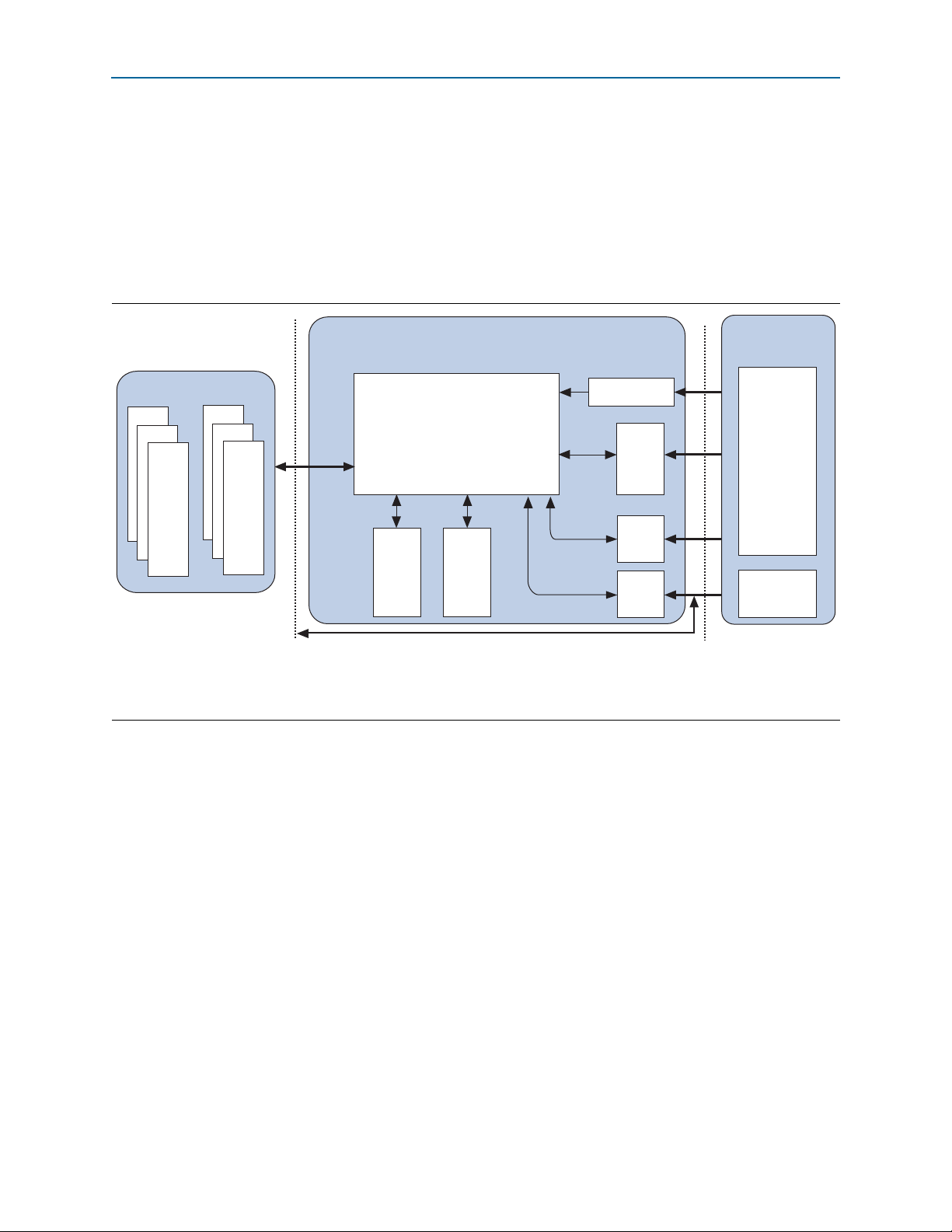
PCI Express
Protocol Stack
Adapter
Clock & Re se t
Se lectio n
PCIe Hard IP Block
TL
Interface
FPGA Fabric Interface
PIPE Interface
LMI
PCIe
Reconfig
Buffer
Virtual
Channel
Buffer
Retry
PCIe Hard IP Block Reconfiguration
RX
FPGA Fabric
Application
Layer
Test, Debug &
Configuration
Logic
PMA
PCS
Transceivers
General Description
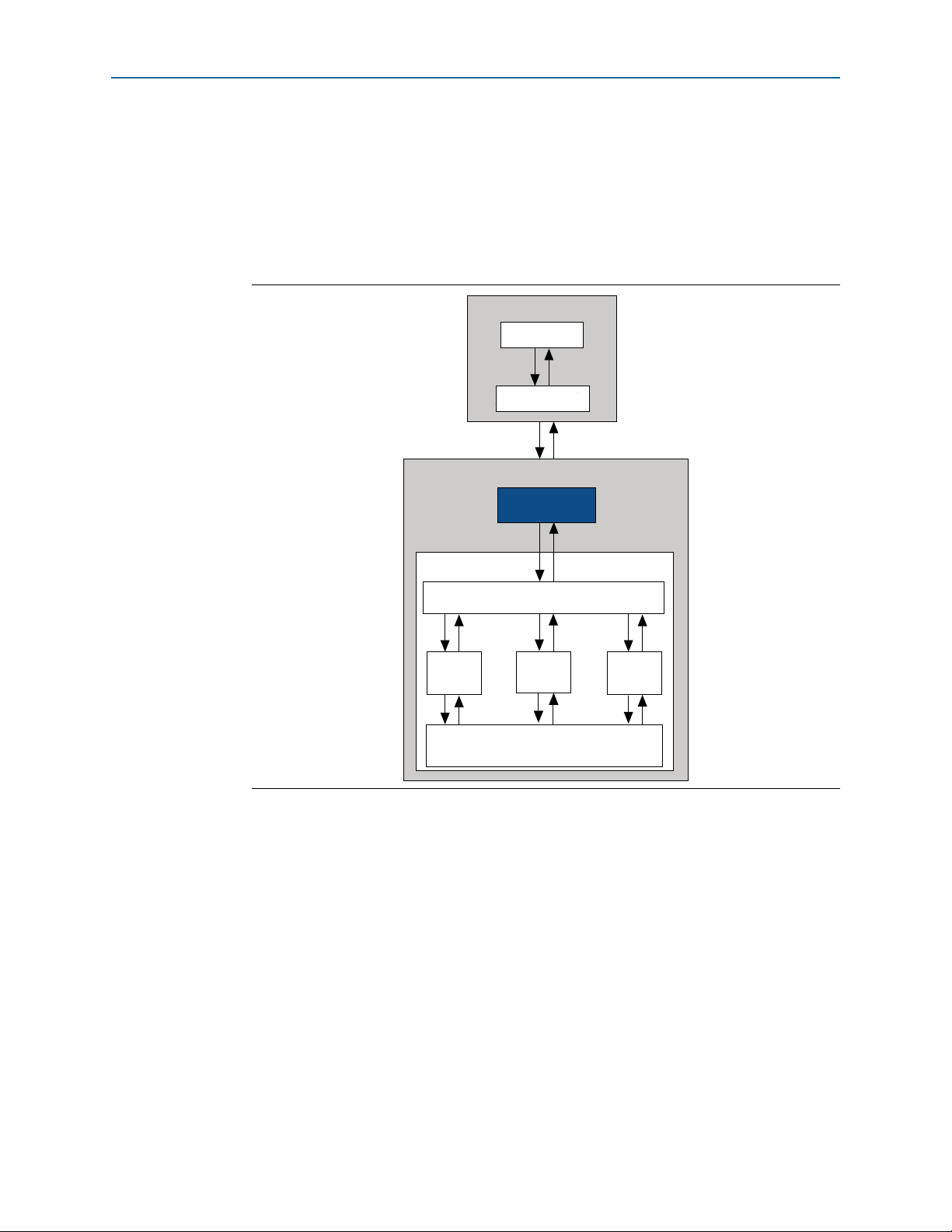
The hard IP implementation includes all of the required and most of the optional
features of the specification for the transaction, data link, and physical layers.
Depending upon the device you choose, one to four instances of the IP Compiler for
PCI Express hard implementation are available. These instances can be configured to
include any combination of root port and endpoint designs to meet your system
requirements. A single device can also use instances of both the soft and hard
implementations of the IP Compiler for PCI Express. Figure 1–1 provides a high-level
block diagram of the hard IP implementation.
Figure 1–1. IP Compiler for PCI Express Hard IP Implementation High-Level Block Diagram (Note 1) (2)
Notes to Figure 1–1:
(1) Stratix IV GX devices have two virtual channels.
(2) LMI stands for Local Management Interface.
This user guide includes a design example and testbench that you can configure as a
root port (RP) or endpoint (EP). You can use these design examples as a starting point
to create and test your own root port and endpoint designs.
f The purpose of the IP Compiler for PCI Express User Guide is to explain how to use the
IP Compiler for PCI Express and not to explain the PCI Express protocol. Although
there is inevitable overlap between the two documents, this document should be used
in conjunction with an understanding of the following PCI Express specifications:
PHY Interface for the PCI Express Architecture PCI Express 3.0 and PCI Express Base
Specification 1.0a, 1.1, or 2.0.
Support for IP Compiler for PCI Express Hard IP
If you target an Arria II GX, Arria II GZ, Cyclone IV GX, or Stratix IV GX device, you
can parameterize the IP core to include a full hard IP implementation of the PCI
Express stack including the following layers:
August 2014 Altera Corporation IP Compiler for PCI Express
■ Physical (PHY)
■ Physical Media Attachment (PMA)
Page 8

1–6 Chapter 1: Datasheet
■ Physical Coding Sublayer (PCS)
■ Media Access Control (MAC)
■ Data link
■ Transaction
General Description
Optimized for Altera devices, the hard IP implementation supports all memory, I/O,
configuration, and message transactions. The IP cores have a highly optimized
application interface to achieve maximum effective throughput. Because the compiler
is parameterizeable, you can customize the IP cores to meet your design
requirements.Table 1–5 lists the configurations that are available for the IP Compiler
for PCI Express hard IP implementation.
Table 1–5. Hard IP Configurations for the IP Compiler for PCI Express in Quartus II Software Version 11.0
Device Link Rate (Gbps) ×1 ×2 (1) ×4 ×8
Avalon Streaming (Avalon-ST) Interface
Arria II GX
Arria II GZ
Cyclone IV GX
Stratix IV GX
2.5 yes no yes yes (2)
5.0 nononono
2.5 yes no yes yes (2)
5.0 yes no yes (2) no
2.5 yes yes yes no
5.0 nononono
2.5 yes no yes yes
5.0 yes no yes yes
Avalon-MM Interface using Qsys Design Flow (3)
Arria II GX 2.5 yes no yes no
Cyclone IV GX 2.5 yes yes yes no
Stratix IV GX
Notes to Table 1–5:
(1) For devices that do not offer a ×2 initial configuration, you can use a ×4 configuration with the upper two lanes left unconnected at the device
pins. The link will negotiate to ×2 if the attached device is ×2 native or capable of negotiating to ×2.
(2) The ×8 support uses a 128-bit bus at 125 MHz.
(3) The Qsys design flow supports the generation of endpoint variations only.
2.5 yes no yes yes
5.0 yes no yes no
Tab le 1– 6 lists the Total RX buffer space, Retry buffer size, and Maximum Payload
size for device families that include the hard IP implementation. You can find these
parameters on the Buffer Setup page of the parameter editor.
Table 1–6. IP Compiler for PCI Express Buffer and Payload Information (Part 1 of 2)
Devices Family Total RX Buffer Space Retry Buffer Max Payload Size
Arria II GX 4 KBytes 2 KBytes 256 Bytes
IP Compiler for PCI Express User Guide August 2014 Altera Corporation
Page 9
Chapter 1: Datasheet 1–7
Altera FPGA with Embedded
PCIe Hard IP Block
User Application
Logic
PCIe
Hard IP
Block
PCIe
Hard IP
Block
RP EP
User Application
Logic
PCI Express Link
Altera FPGA with Embedded
PCIe Hard IP Block
General Description
Table 1–6. IP Compiler for PCI Express Buffer and Payload Information (Part 2 of 2)
Devices Family Total RX Buffer Space Retry Buffer Max Payload Size
Arria II GZ 16 KBytes 16 KBytes 2 KBytes
Cyclone IV GX 4 KBytes 2 KBytes 256 Bytes
Stratix IV GX 16 KBytes 16 KBytes 2 KBytes
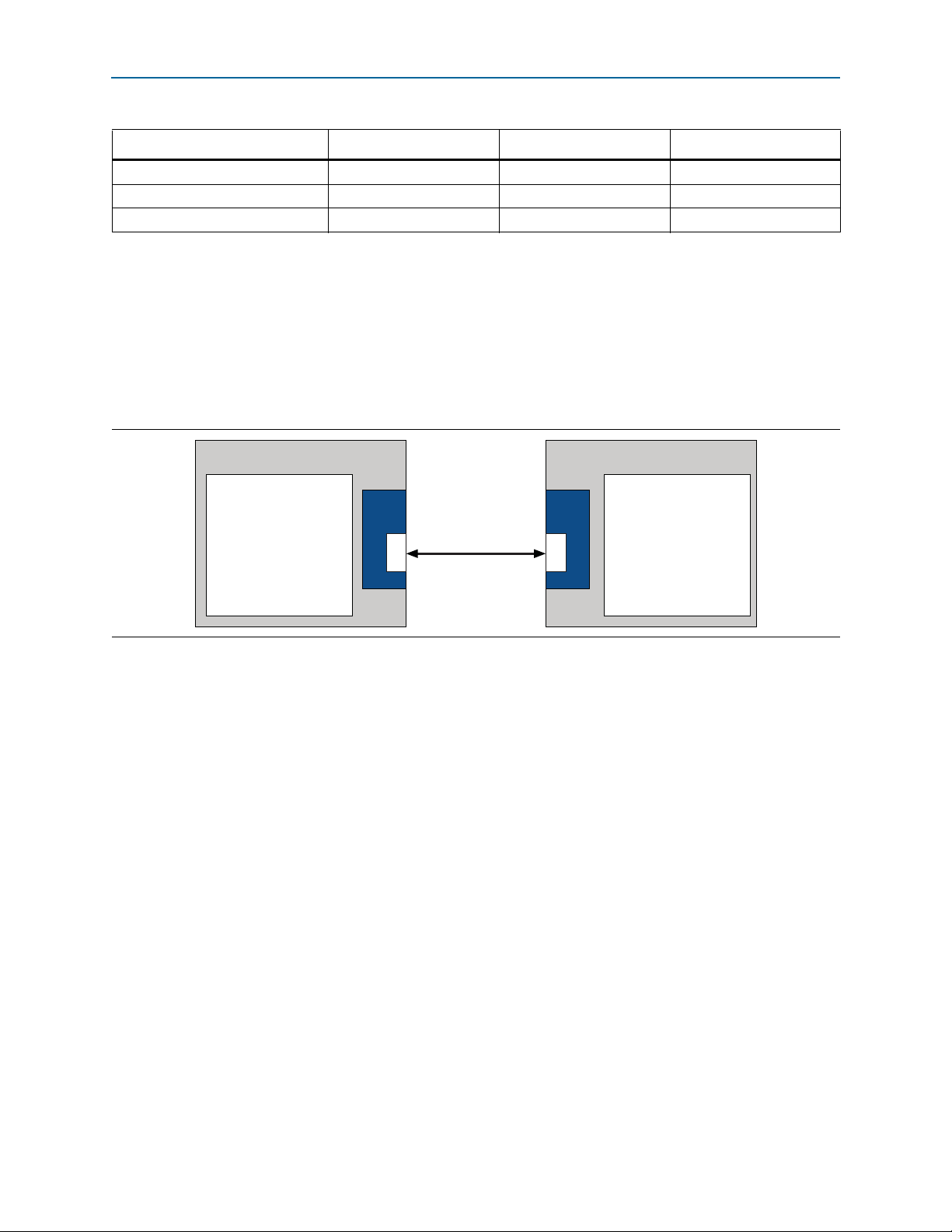
The IP Compiler for PCI Express supports ×1, ×2, ×4, and ×8 variations (Table 1–7 on
page 1–8) that are suitable for either root port or endpoint applications. You can use
the parameter editor to customize the IP core. The Qsys design flows do not support
root port variations. Figure 1–2 shows a relatively simple application that includes
two IP Compilers for PCI Express, one configured as a root port and the other as an
endpoint.
Figure 1–2. PCI Express Application with a Single Root Port and Endpoint
August 2014 Altera Corporation IP Compiler for PCI Express
Page 10
1–8 Chapter 1: Datasheet
PCIe Link
PCIe Hard IP Block
RP
Switch
PCIe
Hard IP
Block
RP
User Application
Logic
PCIe Hard IP Block
EP
PCIe
Hard IP
Block
EP
User Application
Logic
IP Compiler
for
PCI Express
Soft IP
Implementation
EP
User Application
Logic
PHY
PIPE
Interface
User
Application
Logic
PCIe Link
PCIe Link
PCIe Link
PCIe Link
User Application
Logic
Altera FPGA with Embedded PCIe
Hard IP Blocks
Altera FPGA with Embedded PCIe
Hard IP Blocks
Altera FPGA with Embedded PCIe
Hard IP Blocks
Altera FPGA Supporting IP Compiler for
PCI Express Soft IP Implementation
IP Compiler
for
PCI Express
Soft IP
Implementation
General Description
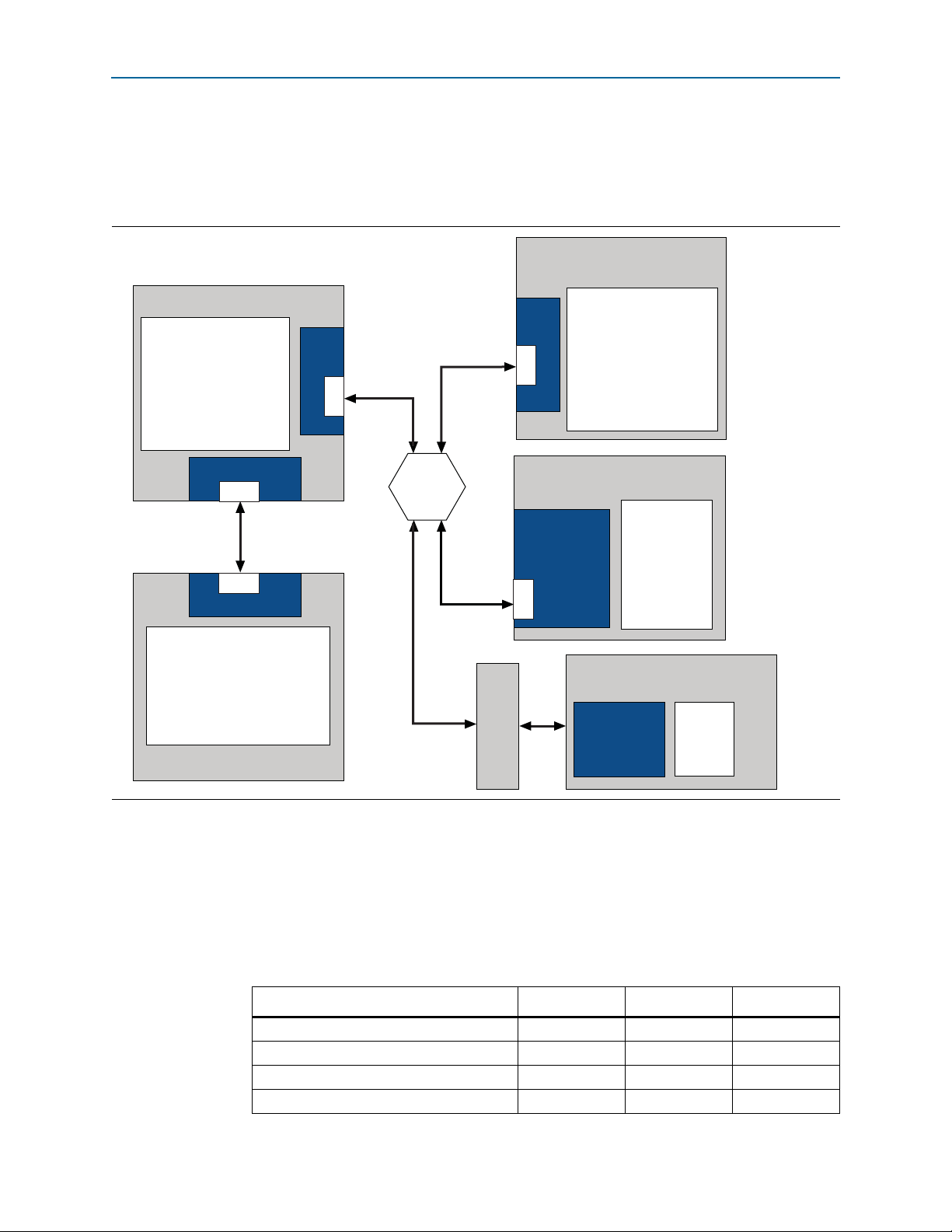
Figure 1–3 illustrates a heterogeneous topology, including an Altera device with two
PCIe hard IP root ports. One root port connects directly to a second FPGA that
includes an endpoint implemented using the hard IP IP core. The second root port
connects to a switch that multiplexes among three PCI Express endpoints.
Figure 1–3. PCI Express Application with Two Root Ports
IP Compiler for PCI Express User Guide August 2014 Altera Corporation
If you target a device that includes an internal transceiver, you can parameterize the
IP Compiler for PCI Express to include a complete PHY layer, including the MAC,
PCS, and PMA layers. If you target other device architectures, the IP Compiler for PCI
Express generates the IP core with the Intel-designed PIPE interface, making the IP
core usable with other PIPE-compliant external PHY devices.
Tab le 1– 7 lists the protocol support for devices that include HSSI transceivers.
Table 1–7. Operation in Devices with HSSI Transceivers (Part 1 of 2) (Note 1)
Device Family ×1 ×4 ×8
Stratix IV GX hard IP–Gen1 Yes Yes Yes
Stratix IV GX hard IP–Gen 2 Yes (2) Yes (2) Yes (3)
Stratix IV soft IP–Gen1 Yes Yes No
Cyclone IV GX hard IP–Gen1 Yes Yes No
Page 11

Chapter 1: Datasheet 1–9
IP Core Verification
Table 1–7. Operation in Devices with HSSI Transceivers (Part 2 of 2) (Note 1)
Device Family ×1 ×4 ×8
Arria II GX–Gen1 Hard IP Implementation Yes Yes Yes
Arria II GX–Gen1 Soft IP Implementation Yes Yes No
Arria II GZ–Gen1 Hard IP Implementation Yes Yes Yes
Arria II GZ–Gen2 Hard IP Implementation Yes Yes No
Notes to Table 1–7:
(1) Refer to Table 1–2 on page 1–2 for a list of features available in the different implementations and design flows.
(2) Not available in -4 speed grade. Requires -2 or -3 speed grade.
(3) Gen2 ×8 is only available in the -2 and I3 speed grades.
1 The device names and part numbers for Altera FPGAs that include internal
transceivers always include the letters GX, GT, or GZ. If you select a device that does
not include an internal transceiver, you can use the PIPE interface to connect to an
external PHY. Table 3–9 on page 3–8 lists the available external PHY types.
You can customize the payload size, buffer sizes, and configuration space (base
address registers support and other registers). Additionally, the IP Compiler for PCI
Express supports end-to-end cyclic redundancy code (ECRC) and advanced error
reporting for ×1, ×2, ×4, and ×8 configurations.
External PHY Support
Altera IP Compiler for PCI Express variations support a wide range of PHYs,
including the TI XIO1100 PHY in 8-bit DDR/SDR mode or 16-bit SDR mode; NXP
PX1011A for 8-bit SDR mode, a serial PHY, and a range of custom PHYs using
8-bit/16-bit SDR with or without source synchronous transmit clock modes and 8-bit
DDR with or without source synchronous transmit clock modes. You can constrain TX
I/Os by turning on the Fast Output Enable Register option in the parameter editor,
or by editing this setting in the Quartus II Settings File (.qsf). This constraint ensures
fastest t
Debug Features
The IP Compiler for PCI Express also includes debug features that allow observation
and control of the IP cores for faster debugging of system-level problems.
f For more information about debugging refer to Chapter 17, Debugging.
IP Core Verification
To ensure compliance with the PCI Express specification, Altera performs extensive
validation of the IP Compiler for PCI Express. Validation includes both simulation
and hardware testing.
timing.
CO
August 2014 Altera Corporation IP Compiler for PCI Express
Page 12

1–10 Chapter 1: Datasheet
Performance and Resource Utilization
Simulation Environment
Altera’s verification simulation environment for the IP Compiler for PCI Express uses
multiple testbenches that consist of industry-standard BFMs driving the PCI Express
link interface. A custom BFM connects to the application-side interface.
Altera performs the following tests in the simulation environment:
■ Directed tests that test all types and sizes of transaction layer packets and all bits of
the configuration space
■ Error injection tests that inject errors in the link, transaction layer packets, and data
link layer packets, and check for the proper response from the IP cores
■ PCI-SIG
■ Random tests that test a wide range of traffic patterns across one or more virtual
®
Compliance Checklist tests that specifically test the items in the checklist
channels
Compatibility Testing Environment
Altera has performed significant hardware testing of the IP Compiler for PCI Express
to ensure a reliable solution. The IP cores have been tested at various PCI-SIG PCI
Express Compliance Workshops in 2005–2009 with Arria GX, Arria II GX,
Cyclone IV GX, Stratix II GX, and Stratix IV GX devices and various external PHYs.
They have passed all PCI-SIG gold tests and interoperability tests with a wide
selection of motherboards and test equipment. In addition, Altera internally tests
every release with motherboards and switch chips from a variety of manufacturers.
All PCI-SIG compliance tests are also run with each IP core release.
Performance and Resource Utilization
The hard IP implementation of the IP Compiler for PCI Express is available in
Arria II GX, Arria II GZ, Cyclone IV GX, and Stratix IV GX devices.
Tab le 1– 8 shows the resource utilization for the hard IP implementation using either
the Avalon-ST or Avalon-MM interface with a maximum payload of 256 bytes and 32
tags for the Avalon-ST interface and 16 tags for the Avalon-MM interface.
Table 1–8. Performance and Resource Utilization in Arria II GX, Arria II GZ, Cyclone IV GX, and
Stratix IV GX Devices (Part 1 of 2)
Parameters Size
Lane
Width
×1 125 1 100 100 0
×1 125 2 100 100 0
×4 125 1 200 200 0
×4 125 2 200 200 0
×8 250 1 200 200 0
×8 250 2 200 200 0
Internal
Clock (MHz)
Virtual
Channel
Combinational
Avalon-ST Interface
ALUTs
Dedicated
Registers
Memory Blocks
M9K
IP Compiler for PCI Express User Guide August 2014 Altera Corporation
Page 13
Chapter 1: Datasheet 1–11
Recommended Speed Grades
Table 1–8. Performance and Resource Utilization in Arria II GX, Arria II GZ, Cyclone IV GX, and
Stratix IV GX Devices (Part 2 of 2)
Parameters Size
Lane
Width
×4 125 1
×1 125 1
×8 250 1
×1 125 1
×4 125 1
×1 125 1
×4 250 1
Note to Tab le 1 –8:
(1) The transaction layer of the Avalon-MM implementation is implemented in programmable logic to improve latency.
Internal
Clock (MHz)
Avalon-MM Interface–Qsys Design Flow - Completer Only Single Dword
Virtual
Channel
Avalon-MM Interface–Qsys Design Flow
Avalon-MM Interface–Qsys Design Flow - Completer Only
Combinational
ALUTs
1600 1600 18 ×4 125 1
1000 1150 10
430 450 0 ×4 125 1
Dedicated
Registers
Memory Blocks
M9K
f Refer to Appendix C, Performance and Resource Utilization Soft IP Implementation
for performance and resource utilization for the soft IP implementation.
Recommended Speed Grades
Tab le 1– 9 shows the recommended speed grades for each device family for the
supported link widths and internal clock frequencies. For soft IP implementations of
the IP Compiler for PCI Express, the table lists speed grades that are likely to meet
timing; it may be possible to close timing in a slower speed grade. For the hard IP
implementation, the speed grades listed are the only speed grades that close timing.
When the internal clock frequency is 125 MHz or 250 MHz, Altera recommends
setting the Quartus II Analysis & Synthesis Settings Optimization Technique to
Speed.
August 2014 Altera Corporation IP Compiler for PCI Express
Page 14

1–12 Chapter 1: Datasheet
Recommended Speed Grades
f Refer to “Setting Up and Running Analysis and Synthesis” in Quartus II Help and
Area and Timing Optimization in volume 2 of the Quartus II Handbook for more
information about how to effect this setting.
Table 1–9. Recommended Device Family Speed Grades (Part 1 of 2)
Device Family Link Width
Internal Clock
Frequency (MHz)
Recommended
Speed Grades
Avalon-ST Hard IP Implementation
×1 62.5 (2) –4,–5,–6
Arria II GX Gen1 with ECC Support (1)
×1 125 –4,–5,–6
×4 125 –4,–5,–6
×8 125 –4,–5,–6
×1 125 -3, -4
Arria II GZ Gen1 with ECC Support
×4 125 -3, -4
×8 125 -3, -4
Arria II GZ Gen 2 with ECC Support
Cyclone IV GX Gen1 with ECC Support
×1 125 -3
×4 125 -3
×1 62.5 (2) all speed grades
×1, ×2, ×4 125 all speed grades
×1 62.5 (2) –2, –3 (3)
Stratix IV GX Gen1 with ECC Support (1)
×1 125 –2, –3, –4
×4 125 –2, –3, –4
×8 250 –2, –3, –4 (3)
Stratix IV GX Gen2 with ECC Support (1)
×1 125 –2, –3 (3)
×4 250 –2, –3 (3)
Stratix IV GX Gen2 without ECC Support ×8 500 –2, I3 (4)
Avalon–MM Interface–Qsys Flow
Arria II GX ×1, ×4 125 –6
Cyclone IV GX
Stratix IV GX Gen1
Stratix IV GX Gen2
×1, ×2, ×4 125 –6, –7
×1 62.5 –6, –7, –8
×1, ×4 125 –2, –3, –4
×8 250 –2, –3
×1 125 –2, –3
×4 250 –2, –3
Avalon-ST or Descriptor/Data Interface Soft IP Implementation
Arria II GX ×1, ×4 125 –4. –5 (5)
Cyclone IV GX ×1 125 –6, –7 (5)
Stratix IV E Gen1
IP Compiler for PCI Express User Guide August 2014 Altera Corporation
×1 62.5 all speed grades
×1, ×4 125 all speed grades
Page 15

Chapter 1: Datasheet 1–13
Recommended Speed Grades
Table 1–9. Recommended Device Family Speed Grades (Part 2 of 2)
Device Family Link Width
Stratix IV GX Gen1
Notes to Table 1–9:
(1) The RX Buffer and Retry Buffer ECC options are only available in the hard IP implementation.
(2) This is a power-saving mode of operation.
(3) Final results pending characterization by Altera for speed grades -2, -3, and -4. Refer to the .fit.rpt file generated
by the Quartus II software.
(4) Closing timing for the –3 speed grades in the provided endpoint example design requires seed sweeping.
(5) You must turn on the following Physical Synthesis settings in the Quartus II Fitter Settings to achieve timing
closure for these speed grades and variations: Perform physical synthesis for combinational logic, Perform
register duplication, and Perform register retiming. In addition, you can use the Quartus II Design Space
Explorer or Quartus II seed sweeping methodology. Refer to the Netlist Optimizations and Physical Synthesis
chapter in volume 2 of the Quartus II Handbook for more information about how to set these options.
(6) Altera recommends disabling the OpenCore Plus feature for the ×8 soft IP implementation because including this
feature makes it more difficult to close timing.
×1 62.5 all speed grades
×4 125 all speed grades
Internal Clock
Frequency (MHz)
Recommended
Speed Grades
August 2014 Altera Corporation IP Compiler for PCI Express
Page 16

1–14 Chapter 1: Datasheet
Recommended Speed Grades
IP Compiler for PCI Express User Guide August 2014 Altera Corporation
Page 17
acds
quartus - Contains the Quartus II software
ip - Contains the Altera IP Library and third-party IP cores
altera - Contains the Altera IP Library source code
<IP core name> - Contains the IP core source files
August 2014
<edit Part Number variable in chapter>
This section provides step-by-step instructions to help you quickly set up and
simulate the IP Compiler for PCI Express testbench. The IP Compiler for PCI Express
provides numerous configuration options. The parameters chosen in this chapter are
the same as those chosen in the PCI Express High-Performance Reference Design
available on the Altera website.
Installing and Licensing IP Cores
The Altera IP Library provides many useful IP core functions for production use
without purchasing an additional license. You can evaluate any Altera IP core in
simulation and compilation in the Quartus II software using the OpenCore evaluation
feature.
Some Altera IP cores, such as MegaCore
separate license for production use. You can use the OpenCore Plus feature to
evaluate IP that requires purchase of an additional license until you are satisfied with
the functionality and performance. After you purchase a license, visit the Self Service
Licensing Center to obtain a license number for any Altera product. For additional
information, refer to Altera Software Installation and Licensing.
Figure 2–1. IP core Installation Path
2. Getting Started
®
functions, require that you purchase a
1 The default installation directory on Windows is <drive>:\altera\<version number>;
on Linux it is <home directory>/altera/<version number>.
OpenCore Plus IP Evaluation
Altera's free OpenCore Plus feature allows you to evaluate licensed MegaCore IP
cores in simulation and hardware before purchase. You need only purchase a license
for MegaCore IP cores if you decide to take your design to production. OpenCore Plus
supports the following evaluations:
■ Simulate the behavior of a licensed IP core in your system.
■ Verify the functionality, size, and speed of the IP core quickly and easily.
■ Generate time-limited device programming files for designs that include IP cores.
■ Program a device with your IP core and verify your design in hardware
OpenCore Plus evaluation supports the following two operation modes:
■ Untethered—run the design containing the licensed IP for a limited time.
August 2014 Altera Corporation IP Compiler for PCI Express User Guide
Page 18

2–2 Chapter 2: Getting Started
■ Tethered—run the design containing the licensed IP for a longer time or
IP Catalog and Parameter Editor
indefinitely. This requires a connection between your board and the host
computer.
All IP cores that use OpenCore Plus time out simultaneously when any IP core in the
design times out.
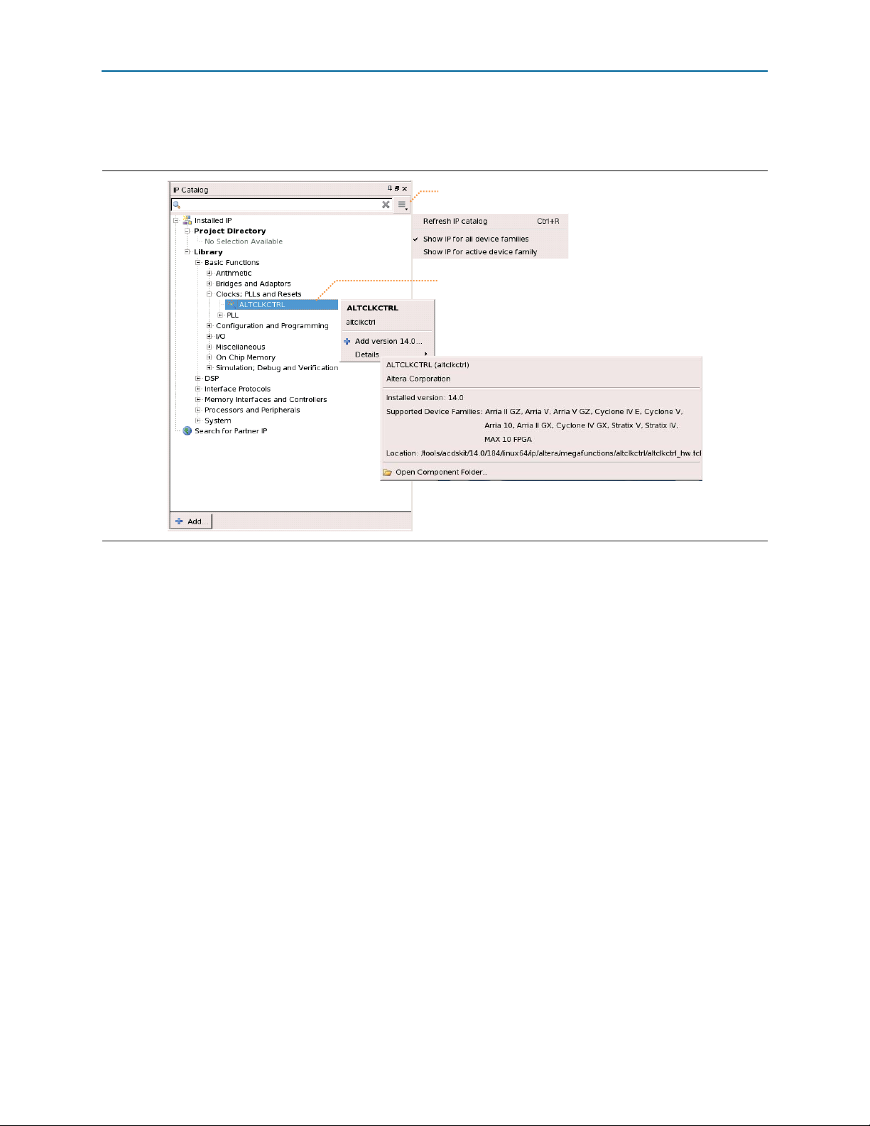
IP Catalog and Parameter Editor
The Quartus II IP Catalog (Too ls > I P C a t a lo g) and parameter editor help you easily
customize and integrate IP cores into your project. You can use the IP Catalog and
parameter editor to select, customize, and generate files representing your custom IP
variation.
1 The IP Catalog (To ol s > IP C a t al og ) and parameter editor replace the MegaWizard™
Plug-In Manager for IP selection and parameterization, beginning in Quartus II
software version 14.0. Use the IP Catalog and parameter editor to locate and
paramaterize Altera IP cores.
The IP Catalog lists IP cores available for your design. Double-click any IP core to
launch the parameter editor and generate files representing your IP variation. The
parameter editor prompts you to specify an IP variation name, optional ports, and
output file generation options. The parameter editor generates a top level Qsys
system file (.qsys) or Quartus II IP file (.qip) representing the IP core in your project.
You can also parameterize an IP variation without an open project.
Use the following features to help you quickly locate and select an IP core:
■ Filter IP Catalog to Show IP for active device family or Show IP for all device
families.
■ Search to locate any full or partial IP core name in IP Catalog. Click Search for
Partner IP, to access partner IP information on the Altera website.
IP Compiler for PCI Express User Guide August 2014 Altera Corporation
Page 19
Chapter 2: Getting Started 2–3
IP Catalog and Parameter Editor
■ Right-click an IP core name in IP Catalog to display details about supported
devices, installation location, and links to documentation.
Figure 2–2. Quartus II IP Catalog
Search and filter IP for your target device
Double-click to customize, right-click for information
1 The IP Catalog is also available in Qsys (View > IP Catalog). The Qsys IP Catalog
includes exclusive system interconnect, video and image processing, and other
system-level IP that are not available in the Quartus II IP Catalog.
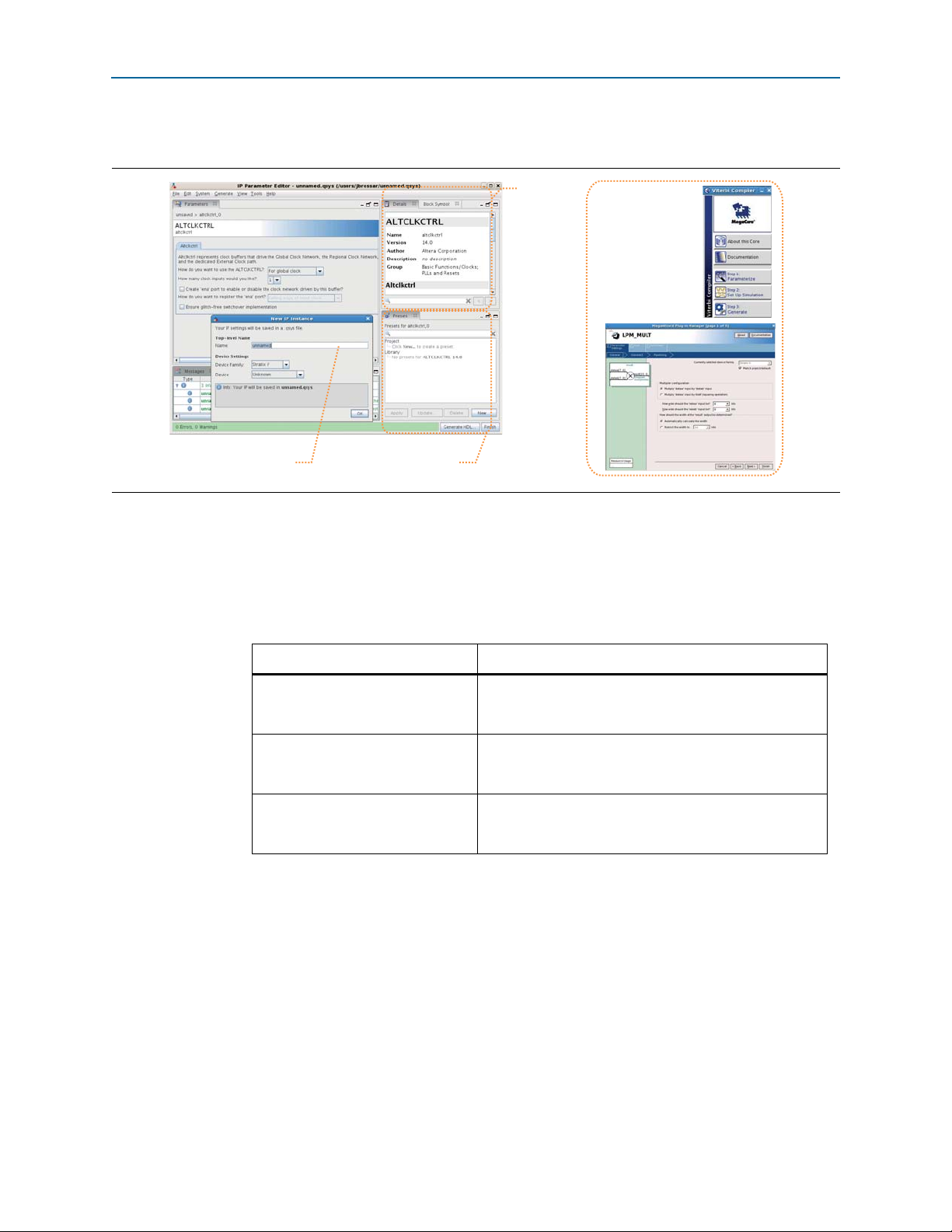
Using the Parameter Editor
The parameter editor helps you to configure your IP variation ports, parameters,
architecture features, and output file generation options:
■ Use preset settings in the parameter editor (where provided) to instantly apply
preset parameter values for specific applications.
■ View port and parameter descriptions and links to detailed documentation.
August 2014 Altera Corporation IP Compiler for PCI Express User Guide
Page 20
2–4 Chapter 2: Getting Started
View IP port
and parameter
details
Apply preset parameters for
specific applications
Specify your IP variation name
and target device
Legacy parameter
editors
■ Generate testbench systems or example designs (where provided).
Upgrading Outdated IP Cores
Figure 2–3. IP Parameter Editors
Modifying an IP Variation
You can easily modify the parameters of any Altera IP core variation in the parameter
editor to match your design requirements. Use any of the following methods to
modify an IP variation in the parameter editor.
Table 2–1. Modifying an IP Variation
Menu Command Action
File > Open
View > Utility Windows >
Project Navigator > IP Components
Project > Upgrade IP Components
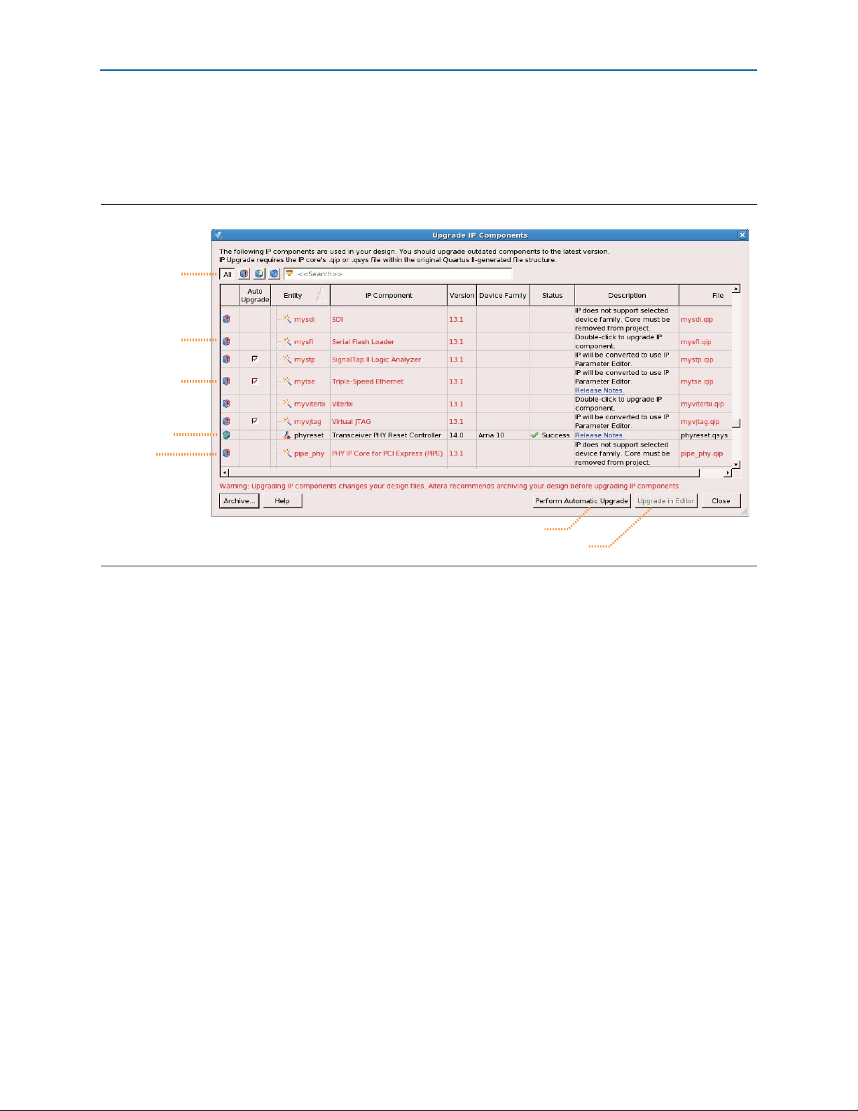
Upgrading Outdated IP Cores
IP core variants generated with a previous version of the Quartus II software may
require upgrading before use in the current version of the Quartus II software. Click
Project > Upgrade IP Components to identify and upgrade IP core variants.
The Upgrade IP Components dialog box provides instructions when IP upgrade is
required, optional, or unsupported for specific IP cores in your design. You must
upgrade IP cores that require it before you can compile the IP variation in the current
version of the Quartus II software. Many Altera IP cores support automatic upgrade.
Select the top-levelHDL(.v, or .vhd) IP variation file to
launch the parameter editor and modify the IP variation.
Regenerate the IP variation to implement your changes.
Double-click the IP variation to launch the parameter
editor and modify the IP variation. Regenerate the IP
variation to implement your changes.
Select the IP variation and click Upgrade in Editor to
launch the parameter editor and modify the IP variation.
Regenerate the IP variation to implement your changes.
IP Compiler for PCI Express User Guide August 2014 Altera Corporation
Page 21

Chapter 2: Getting Started 2–5
Upgrading Outdated IP Cores
The upgrade process renames and preserves the existing variation file (.v, .sv, or .vhd)
as <my_ip>_ BAK.v, .sv, .vhd in the project directory.
Table 2–2. IP Core Upgrade Status
IP Core Status Corrective Action
Required Upgrade IP
Components
You must upgrade the IP variation before compiling in the current
version of the Quartus II software.
Upgrade is optional for this IP variation in the current version of the
Optional Upgrade IP
Components
Quartus II software. You can upgrade this IP variation to take
advantage of the latest development of this IP core. Alternatively you
can retain previous IP core characteristics by declining to upgrade.
Upgrade of the IP variation is not supported in the current version of
the Quartus II software due to IP core end of life or incompatibility
Upgrade Unsupported
with the current version of the Quartus II software. You are prompted
to replace the obsolete IP core with a current equivalent IP core from
the IP Catalog.
Before you begin
■ Archive the Quartus II project containing outdated IP cores in the original version
of the Quartus II software: Click Project > Archive Project to save the project in
your previous version of the Quartus II software. This archive preserves your
original design source and project files.
■ Restore the archived project in the latest version of the Quartus II software: Click
Project > Restore Archived Project. Click OK if prompted to change to a
supported device or overwrite the project database. File paths in the archive must
be relative to the project directory. File paths in the archive must reference the IP
variation .v or .vhd file or .qsys file (not the .qip file).
1. In the latest version of the Quartus II software, open the Quartus II project
containing an outdated IP core variation. The Upgrade IP Components dialog
automatically displays the status of IP cores in your project, along with
instructions for upgrading each core. Click Project > Upgrade IP Components to
access this dialog box manually.
August 2014 Altera Corporation IP Compiler for PCI Express User Guide
Page 22
2–6 Chapter 2: Getting Started
Displays upgrade
status for all IP cores
in the Project
Upgrades all IP core that support “Auto Upgrade”
Upgrades individual IP cores unsupported by “Auto Upgrade”
Checked IP cores
support “Auto Upgrade”
Successful
“Auto Upgrade”
Upgrade
unavailable
Double-click to
individually migrate
Upgrading Outdated IP Cores
2. To simultaneously upgrade all IP cores that support automatic upgrade, click
Perform Automatic Upgrade. The Status and Ve rs i o n columns update when
upgrade is complete. Example designs provided with any Altera IP core
regenerate automatically whenever you upgrade the IP core.
Figure 2–4. Upgrading IP Cores
Upgrading IP Cores at the Command Line
You can upgrade IP cores that support auto upgrade at the command line. IP cores
that do not support automatic upgrade do not support command line upgrade.
■ To upgrade a single IP core that supports auto-upgrade, type the following
command:
quartus_sh –ip_upgrade –variation_files
<qii_project>
Example:
■ To simultaneously upgrade multiple IP cores that support auto-upgrade, type the
quartus_sh -ip_upgrade -variation_files mega/pll25.v hps_testx
following command:
quartus_sh –ip_upgrade –variation_files “
<my_ip_filepath/my_ip2>.<hdl>
Example:
quartus_sh -ip_upgrade -variation_files
”
<qii_project>
"mega/pll_tx2.v;mega/pll3.v" hps_testx
f IP cores older than Quartus II software version 12.0 do not support upgrade. Altera
verifies that the current version of the Quartus II software compiles the previous
version of each IP core. The MegaCore IP Library Release Notes reports any verification
exceptions for MegaCore IP. The Quartus II Software and Device Support Release Notes
reports any verification exceptions for other IP cores. Altera does not verify
compilation for IP cores older than the previous two releases.
<my_ip_filepath/my_ip>.<hdl>
<my_ip_filepath/my_ip1>.<hdl>;
IP Compiler for PCI Express User Guide August 2014 Altera Corporation
Page 23

Chapter 2: Getting Started 2–7
Parameterizing the IP Compiler for PCI Express
Parameterizing the IP Compiler for PCI Express
This section guides you through the process of parameterizing the IP Compiler for
PCI Express as an endpoint, using the same options that are chosen in Chapter 15,
Testbench and Design Example. Complete the following steps to specify the
parameters:
1. In the IP Catalog (Tools > IP Catalog), locate and double-click the name of the IP
core to customize. The parameter editor appears.
2. Specify a top-level name for your custom IP variation. This name identifies the IP
core variation files in your project. For this walkthrough, specify top.v for the
name of the IP core file: <working_dir>\top.v.
3. Specify the following values in the parameter editor:
Table 2–3. System Settings Parameters
Parameter Value
PCIe Core Type PCI Express hard IP
PHY type Stratix IV GX
PHY interface serial
Configure transceiver block Use default settings.
Lanes ×8
Xcvr ref_clk 100 MHz
Application interface Avalon-ST 128 -bit
Port type Native Endpoint
PCI Express version 2.0
Application clock 250 MHz
Max rate Gen 2 (5.0 Gbps)
Test out width 64 bits
HIP reconfig Disable
4. To enable all of the tests in the provided testbench and chaining DMA example
design, make the base address register (BAR) assignments. Bar2 or Bar3 is
required.Table 2–4. provides the BAR assignments in tabular format.
Table 2–4. PCI Registers (Part 1 of 2)
PCI Base Registers (Type 0 Configuration Space)
BAR BAR TYPE BAR Size
0 32-Bit Non-Prefetchable Memory 256 MBytes - 28 bits
1 32-Bit Non-Prefetchable Memory 256 KBytes - 18 bits
2 32-bit Non-Prefetchable Memory 256 KBytes -18 bits
PCI Read-Only Registers
Register Name Value
Device ID
Subsystem ID
Revision ID
Vendor ID
August 2014 Altera Corporation IP Compiler for PCI Express User Guide
0xE001
0x2801
0x01
0x1172
Page 24

2–8 Chapter 2: Getting Started
Parameterizing the IP Compiler for PCI Express
Table 2–4. PCI Registers (Part 2 of 2)
PCI Base Registers (Type 0 Configuration Space)
Subsystem vendor ID
Class code
0x5BDE
0xFF0000
5. Specify the following settings for the Capabilities parameters.
Table 2–5. Capabilities Parameters
Parameter Value
Device Capabilities
Tags supported 32
Implement completion timeout disable Turn this option On
Completion timeout range ABCD
Error Reporting
Implement advanced error reporting Off
Implement ECRC check Off
Implement ECRC generation Off
Implement ECRC forwarding Off
MSI Capabilities
MSI messages requested 4
MSI message 64–bit address capable On
Link Capabilities
Link common clock On
Data link layer active reporting Off
Surprise down reporting Off
Link port number 0x01
Slot Capabilities
Enable slot capability Off
Slot capability register 0x0000000
MSI-X Capabilities
Implement MSI-X Off
Table size 0x000
Offset 0x00000000
BAR indicator (BIR) 0
Pending Bit Array (PBA)
Offset 0x00000000
BAR Indicator 0
IP Compiler for PCI Express User Guide August 2014 Altera Corporation
Page 25

Chapter 2: Getting Started 2–9
Parameterizing the IP Compiler for PCI Express
6. Click the Buffer Setup tab to specify settings on the Buffer Setup page.
Table 2–6. Buffer Setup Parameters
Parameter Value
Maximum payload size 512 bytes
Number of virtual channels 1
Number of low-priority VCs None
Auto configure retry buffer size On
Retry buffer size 16 KBytes
Maximum retry packets 64
Desired performance for received requests Maximum
Desired performance for received completions Maximum
1 For the PCI Express hard IP implementation, the RX Buffer Space Allocation is fixed
at Maximum performance. This setting determines the values for a read-only table
that lists the number of posted header credits, posted data credits, non-posted header
credits, completion header credits, completion data credits, total header credits, and
total RX buffer space.
7. Specify the following power management settings.
Table 2–7. Power Management Parameters
Parameter Value
L0s Active State Power Management (ASPM)
Idle threshold for L0s entry 8,192 ns
Endpoint L0s acceptable latency < 64 ns
Number of fast training sequences (N_FTS)
Common clock Gen2: 255
Separate clock Gen2: 255
Electrical idle exit (EIE) before FTS 4
L1s Active State Power Management (ASPM)
Enable L1 ASPM Off
Endpoint L1 acceptable latency < 1 µs
L1 Exit Latency Common clock > 64 µs
L1 Exit Latency Separate clock > 64 µs
8. On the EDA tab, turn on Generate simulation model to generate an IP functional
simulation model for the IP core. An IP functional simulation model is a
cycle-accurate VHDL or Verilog HDL model produced by the Quartus II software.
c Use the simulation models only for simulation and not for synthesis or any
other purposes. Using these models for synthesis creates a non-functional
design.
August 2014 Altera Corporation IP Compiler for PCI Express User Guide
Page 26
2–10 Chapter 2: Getting Started
<working_dir>
<variation>.v = top.v, the parameterized PCI Express IP Core
<variation>.sdc = top.sdc, the timing constraints file
<variation>.tcl = top.tcl, general Quartus II settings
<variation>_examples = top_examples
ip_compiler_for_pci_express-library
contains local copy of the pci express library files needed for
simulation, or compilation, or both
Testbench and
Design Example
Files
IP Compiler for
PCI Express
Files
Includes testbench and incremental compile directories
common
chaining_dma, files to implement the chaining DMA
top_example_chaining_top.qpf, the Quartus II project file
top_example_chaining_top.qsf, the Quartus II settings file
<variation>
_plus.v = top_plus.v,
the parameterized PCI Express IP Core including reset and
calibration circuitry
testbench, scripts to run the testbench
runtb.do, script to run the testbench
<variation>_chaining_testbench = top_chaining_testbench.v
altpcietb_bfm_driver_chaining.v , provides test stimulus
Simulation and
Quartus II
Compilation
(1) (2)
Viewing the Generated Files
9. On the Summary tab, select the files you want to generate. A gray checkmark
indicates a file that is automatically generated. All other files are optional.
10. Click Finish to generate the IP core, testbench, and supporting files.
1 A report file,
<
variation name>.html, in your project directory lists each file
generated and provides a description of its contents.
Viewing the Generated Files
Figure 2–5 illustrates the directory structure created for this design after you generate
the IP Compiler for PCI Express. The directories includes the following files:
■ The IP Compiler for PCI Express design files, stored in <working_dir>.
■ The chaining DMA design example file, stored in the
<working_dir>\top_examples\chaining_dma directory. This design example tests
your generated IP Compiler for PCI Express variation. For detailed information
about this design example, refer to Chapter 15, Testbench and Design Example.
■ The simulation files for the chaining DMA design example, stored in the
<working_dir>\top_examples\chaining_dma\testbench directory. The Quartus II
software generates the testbench files if you turn on Generate simulation model
on the EDA tab while generating the IP Compiler for PCI Express.
0
Figure 2–5. Directory Structure for IP Compiler for PCI Express and Testbench
Notes to Figure 2–5:
(1) The chaining_dma directory contains the Quartus II project and settings files.
(2) <variation>_plus.v is only available for the hard IP implementation.
IP Compiler for PCI Express User Guide August 2014 Altera Corporation
Page 27
Chapter 2: Getting Started 2–11
Viewing the Generated Files
Figure 2–6 illustrates the top-level modules of this design. As this figure illustrates,
the IP Compiler for PCI Express connects to a basic root port bus functional model
(BFM) and an application layer high-performance DMA engine. These two modules,
when combined with the IP Compiler for PCI Express, comprise the complete
example design. The test stimulus is contained in altpcietb_bfm_driver_chaining.v.
The script to run the tests is runtb.do. For a detailed explanation of this example
design, refer to Chapter 15, Testbench and Design Example.
Figure 2–6. Testbench for the Chaining DMA Design Example
Root Port BFM
Root Port Driver
x8 Root Port Model
PCI Express Link
Endpoint Example
IP Compiler
for PCI Express
Endpoint Application
Layer Example
Traffic Control/Virtual Channel Mapping
Request/Completion Routing
RC
Slave
(Optional)
DMA
Write
Endpoint
Memory
(32 KBytes)
DMA
Read
f The design files used in this design example are the same files that are used for the
PCI Express High-Performance Reference Design. You can download the required
files on the PCI Express High-Performance Reference Design product page. This
product page includes design files for various devices. The example in this document
uses the Stratix IV GX files. You can generate, simulate, and compile the design
example with the files and capabilities provided in your Quartus II software and IP
installation. However, to configure the example on a device, you must also download
altpcie_demo.zip, which includes a software driver that the example design uses,
from the PCI Express High-Performance Reference Design.
August 2014 Altera Corporation IP Compiler for PCI Express User Guide
Page 28

2–12 Chapter 2: Getting Started
Simulating the Design
The Stratix IV .zip file includes files for Gen1 and Gen2 ×1, ×4, and ×8 variants. The
example in this document demonstrates the Gen2 ×8 variant. After you download
and unzip this .zip file, you can copy the files for this variant to your project directory,
<working_dir>. The files for the example in this document are included in the
hip_s4gx_gen2x8_128 directory. The Quartus II project file, top.qsf, is contained in
<working_dir>. You can use this project file as a reference for the .qsf file for your own
design.
Simulating the Design
As Figure 2–5 illustrates, the scripts to run the simulation files are located in the
<working_dir>\top_examples\chaining_dma\testbench directory. Follow these
steps to run the chaining DMA testbench.
1. Start your simulation tool. This example uses the ModelSim
1 The endpoint chaining DMA design example DMA controller requires the
use of BAR2 or BAR3.
2. In the testbench directory,
<working_dir>\top_examples\chaining_dma\testbench, type the following
command:
®
software.
do runtb.do
r
This script compiles the testbench for simulation and runs the chaining DMA
tests.
Example 2–1 shows the partial transcript from a successful simulation. As this
transcript illustrates, the simulation includes the following stages:
■ Link training
■ Configuration
■ DMA reads and writes
IP Compiler for PCI Express User Guide August 2014 Altera Corporation
Page 29

Chapter 2: Getting Started 2–13
Simulating the Design
■ Root port to endpoint memory reads and writes
Example 2–1. Excerpts from Transcript of Successful Simulation Run
Time: 56000 Instance: top_chaining_testbench.ep.epmap.pll_250mhz_to_500mhz.
altpll_component.pll0
# INFO: 464 ns Completed initial configuration of Root Port.
# INFO: Core Clk Frequency: 251.00 Mhz
# INFO: 3608 ns EP LTSSM State: DETECT.ACTIVE
# INFO: 3644 ns EP LTSSM State: POLLING.ACTIVE
# INFO: 3660 ns RP LTSSM State: DETECT.ACTIVE
# INFO: 3692 ns RP LTSSM State: POLLING.ACTIVE
# INFO: 6012 ns RP LTSSM State: POLLING.CONFIG
# INFO: 6108 ns EP LTSSM State: POLLING.CONFIG
# INFO: 7388 ns EP LTSSM State: CONFIG.LINKWIDTH.START
# INFO: 7420 ns RP LTSSM State: CONFIG.LINKWIDTH.START
# INFO: 7900 ns EP LTSSM State: CONFIG.LINKWIDTH.ACCEPT
# INFO: 8316 ns RP LTSSM State: CONFIG.LINKWIDTH.ACCEPT
# INFO: 8508 ns RP LTSSM State: CONFIG.LANENUM.WAIT
# INFO: 9004 ns EP LTSSM State: CONFIG.LANENUM.WAIT
# INFO: 9196 ns EP LTSSM State: CONFIG.LANENUM.ACCEPT
# INFO: 9356 ns RP LTSSM State: CONFIG.LANENUM.ACCEPT
# INFO: 9548 ns RP LTSSM State: CONFIG.COMPLETE
# INFO: 9964 ns EP LTSSM State: CONFIG.COMPLETE
# INFO: 11052 ns EP LTSSM State: CONFIG.IDLE
# INFO: 11276 ns RP LTSSM State: CONFIG.IDLE
# INFO: 11356 ns RP LTSSM State: L0
# INFO: 11580 ns EP LTSSM State: L0
August 2014 Altera Corporation IP Compiler for PCI Express User Guide
Page 30

2–14 Chapter 2: Getting Started
Simulating the Design
Example 2-1 continued
## INFO: 12536 ns
# INFO: 15896 ns EP PCI Express Link Status Register (1081):
# INFO: 15896 ns Negotiated Link Width: x8
# INFO: 15896 ns Slot Clock Config: System Reference Clock Used
# INFO: 16504 ns RP LTSSM State: RECOVERY.RCVRLOCK
# INFO: 16840 ns EP LTSSM State: RECOVERY.RCVRLOCK
# INFO: 17496 ns EP LTSSM State: RECOVERY.RCVRCFG
# INFO: 18328 ns RP LTSSM State: RECOVERY.RCVRCFG
# INFO: 20440 ns RP LTSSM State: RECOVERY.SPEED
# INFO: 20712 ns EP LTSSM State: RECOVERY.SPEED
# INFO: 21600 ns EP LTSSM State: RECOVERY.RCVRLOCK
# INFO: 21614 ns RP LTSSM State: RECOVERY.RCVRLOCK
# INFO: 22006 ns RP LTSSM State: RECOVERY.RCVRCFG
# INFO: 22052 ns EP LTSSM State: RECOVERY.RCVRCFG
# INFO: 22724 ns EP LTSSM State: RECOVERY.IDLE
# INFO: 22742 ns RP LTSSM State: RECOVERY.IDLE
# INFO: 22846 ns RP LTSSM State: L0
# INFO: 22900 ns EP LTSSM State: L0
# INFO: 23152 ns Current Link Speed: 5.0GT/s
# INFO: 27936 ns ---------
# INFO: 27936 ns TASK:dma_set_header READ
# INFO: 27936 ns Writing Descriptor header
# INFO: 27976 ns data content of the DT header
# INFO: 27976 ns
# INFO: 27976 ns Shared Memory Data Display:
# INFO: 27976 ns Address Data
# INFO: 27976 ns ------- ----
# INFO: 27976 ns 00000900 00000003 00000000 00000900 CAFEFADE
# INFO: 27976 ns ---------
# INFO: 27976 ns TASK:dma_set_rclast
# INFO: 27976 ns Start READ DMA : RC issues MWr (RCLast=0002)
# INFO: 27992 ns ---------
# INFO: 28000 ns TASK:msi_poll Polling MSI Address:07F0---> Data:FADE......
# INFO: 28092 ns TASK:rcmem_poll Polling RC Address0000090C current data (0000FADE)
expected data (00000002)
# INFO: 29592 ns TASK:rcmem_poll Polling RC Address0000090C current data (00000000)
expected data (00000002)
# INFO: 31392 ns TASK:rcmem_poll Polling RC Address0000090C current data (00000002)
expected data (00000002)
# INFO: 31392 ns TASK:rcmem_poll ---> Received Expected Data (00000002)
# INFO: 31440 ns TASK:msi_poll Received DMA Read MSI(0000) : B0FC
# INFO: 31448 ns Completed DMA Read
# INFO: 31448 ns ---------
# INFO: 31448 ns TASK:chained_dma_test
# INFO: 31448 ns DMA: Write
# INFO: 31448 ns ---------
# INFO: 31448 ns TASK:dma_wr_test
# INFO: 31448 ns DMA: Write
# INFO: 31448 ns ---------
# INFO: 31448 ns TASK:dma_set_wr_desc_data
# INFO: 31448 ns ---------
INFO: 31448 ns TASK:dma_set_msi WRITE
# INFO: 31448 ns Message Signaled Interrupt Configuration
# INFO: 1448 ns msi_address (RC memory)= 0x07F0
# INFO: 31760 ns msi_control_register = 0x00A5
# INFO: 32976 ns msi_expected = 0xB0FD
IP Compiler for PCI Express User Guide August 2014 Altera Corporation
Page 31

Chapter 2: Getting Started 2–15
Simulating the Design
Example 2-1 continued
# INFO: 32976 ns msi_capabilities address = 0x0050
# INFO: 32976 ns multi_message_enable = 0x0002
# INFO: 32976 ns msi_number = 0001
# INFO: 32976 ns msi_traffic_class = 0000
# INFO: 32976 ns ---------
# INFO: 26416 ns TASK:chained_dma_test
# INFO: 26416 ns DMA: Read
# INFO: 26416 ns --------# INFO: 26416 ns TASK:dma_rd_test
# INFO: 26416 ns ---------
# INFO: 26416 ns TASK:dma_set_rd_desc_data
# INFO: 26416 ns ---------
# INFO: 26416 ns TASK:dma_set_msi READ
# INFO: 26416 ns Message Signaled Interrupt Configuration
# INFO: 26416 ns msi_address (RC memory)= 0x07F0
# INFO: 26720 ns msi_control_register = 0x0084
# INFO: 27936 ns msi_expected = 0xB0FC
# INFO: 27936 ns msi_capabilities address = 0x0050
# INFO: 27936 ns multi_message_enable = 0x0002
# INFO: 27936 ns msi_number = 0000
# INFO: 27936 ns msi_traffic_class = 0000
# INFO: 32976 ns TASK:dma_set_header WRITE
# INFO: 32976 ns Writing Descriptor header
# INFO: 33016 ns data content of the DT header
# INFO: 33016 ns
# INFO: 33016 ns Shared Memory Data Display:
# INFO: 33016 ns Address Data
# INFO: 33016 ns ------- ----
# INFO: 33016 ns 00000800 10100003 00000000 00000800 CAFEFADE
# INFO: 33016 ns ---------
# INFO: 33016 ns TASK:dma_set_rclast
# INFO: 33016 ns Start WRITE DMA : RC issues MWr (RCLast=0002)
# INFO: 33032 ns ---------
# INFO: 33038 ns TASK:msi_poll Polling MSI Address:07F0---> Data:FADE......
# INFO: 33130 ns TASK:rcmem_poll Polling RC Address0000080C current data (0000FADE)
expected data (00000002)
# INFO: 34130 ns TASK:rcmem_poll Polling RC Address0000080C current data (00000000)
expected data (00000002)
# INFO: 35910 ns TASK:msi_poll Received DMA Write MSI(0000) : B0FD
# INFO: 35930 ns TASK:rcmem_poll Polling RC Address0000080C current data (00000002)
expected data (00000002)
# INFO: 35930 ns TASK:rcmem_poll ---> Received Expected Data (00000002)
# INFO: 35938 ns ---------
# INFO: 35938 ns Completed DMA Write
# INFO: 35938 ns ---------
# INFO: 35938 ns TASK:check_dma_data
# INFO: 35938 ns Passed : 0644 identical dwords.
# INFO: 35938 ns ---------
# INFO: 35938 ns TASK:downstream_loop
# INFO: 36386 ns Passed: 0004 same bytes in BFM mem addr 0x00000040
and 0x00000840
# INFO: 36826 ns Passed: 0008 same bytes in BFM mem addr 0x00000040 and 0x00000840
# INFO: 37266 ns Passed: 0012 same bytes in BFM mem addr 0x00000040 and 0x00000840
# INFO: 37714 ns Passed: 0016 same bytes in BFM mem addr 0x00000040 and 0x00000840
# INFO: 38162 ns Passed: 0020 same bytes in BFM mem addr 0x00000040 and 0x00000840
# INFO: 38618 ns Passed: 0024 same bytes in BFM mem addr 0x00000040 and 0x00000840
# INFO: 39074 ns Passed: 0028 same bytes in BFM mem addr 0x00000040 and 0x00000840
# INFO: 39538 ns Passed: 0032 same bytes in BFM mem addr 0x00000040 and 0x00000840
# INFO: 40010 ns Passed: 0036 same bytes in BFM mem addr 0x00000040 and 0x00000840
# INFO: 40482 ns Passed: 0040 same bytes in BFM mem addr 0x00000040 and 0x00000840
# SUCCESS: Simulation stopped due to successful completion!
August 2014 Altera Corporation IP Compiler for PCI Express User Guide
Page 32

2–16 Chapter 2: Getting Started
Constraining the Design
Constraining the Design
The Quartus project directory for the chaining DMA design example is in
<working_dir>\top_examples\chaining_dma\. Before compiling the design using
the Quartus II software, you must apply appropriate design constraints, such as
timing constraints. The Quartus II software automatically generates the constraint
files when you generate the IP Compiler for PCI Express.
Tab le 2– 8 describes these constraint files.
Table 2–8. Automatically Generated Constraints Files
Constraint Type Directory Description
This file includes various Quartus II constraints. In
particular, it includes virtual pin assignments. Virtual
General <working_dir>/<variation>.tcl (top.tcl)
Timing <working_dir>/<variation>.sdc (top.sdc)
pin assignments allow you to avoid making specific
pin assignments for top-level signals while you are
simulating and not yet ready to map the design to
hardware.
This file is the Synopsys Design Constraints File (.sdc)
which includes timing constraints.
If you want to perform an initial compilation to check any potential issues without
creating pin assignments for a specific board, you can do so after running the
following two steps that constrain the chaining DMA design example:
1. To apply Quartus II constraint files, type the following commands at the Tcl
console command prompt:
source ../../
top
.tcl
r
1 To display the Quartus II Tcl Console, on the View menu, point to Utility
Windows and click Tc l C o n s o l e .
2. To add the Synopsys timing constraints to your design, follow these steps:
a. On the Assignments menu, click Settings.
b. Click TimeQuest Timing Analyzer.
c. Under SDC files to include in the project, click the Browse button. Browse to
your <working_dir> to add top.sdc.
d. Click Add.
e. Click OK.
IP Compiler for PCI Express User Guide August 2014 Altera Corporation
Page 33

Chapter 2: Getting Started 2–17
Constraining the Design
Example 2–2 illustrates the Synopsys timing constraints.
Example 2–2. Synopsys Timing Constraints
derive_pll_clocks
derive_clock_uncertainty
create_clock -period "100 MHz" -name {refclk} {refclk}
set_clock_groups -exclusive -group [get_clocks { refclk*clkout }] -group [get_clocks {
*div0*coreclkout}]
set_clock_groups -exclusive -group [get_clocks { *central_clk_div0* }] -group
[get_clocks { *_hssi_pcie_hip* }] -group [get_clocks { *central_clk_div1* }]
<The following 4 additional constraints are for Stratix IV ES Silicon only>
set_multicycle_path -from [get_registers *delay_reg*] -to [get_registers *all_one*] hold -start 1
set_multicycle_path -from [get_registers *delay_reg*] -to [get_registers *all_one*] setup -start 2
set_multicycle_path -from [get_registers *align*chk_cnt*] -to [get_registers
*align*chk_cnt*] -hold -start 1
set_multicycle_path -from [get_registers *align*chk_cnt*] -to [get_registers
*align*chk_cnt*] -setup -start 2
Specifying Device and Pin Assignments
If you want to download the design to a board, you must specify the device and pin
assignments for the chaining DMA example design. To make device and pin
assignments, follow these steps:
1. To select the device, on the Assignments menu, click Device.
2. In the Family list, select Stratix IV (GT/GX/E).
3. Scroll through the Available devices to select EP4SGX230KF40C2.
4. To add pin assignments for the EP4SGX230KF40C2 device, copy all the text
included in to the chaining DMA design example .qsf file,
<working_dir>\top_examples\chaining_dma\top_example_chaining_top.qsf to
your project .qsf file.
August 2014 Altera Corporation IP Compiler for PCI Express User Guide
Page 34

2–18 Chapter 2: Getting Started
Constraining the Design
1 The pin assignments provided in the .qsf are valid for the Stratix IV GX
FPGA Development Board and the EP4SGX230KF40C2 device. If you are
using different hardware you must determine the correct pin assignments.
Example 2–3. Pin Assignments for the Stratix IV GX (EP4SGX230KF40C2) FPGA Development Board
set_location_assignment PIN_AK35 -to local_rstn_ext
set_location_assignment PIN_R32 -to pcie_rstn
set_location_assignment PIN_AN38 -to refclk
set_location_assignment PIN_AU38 -to rx_in0
set_location_assignment PIN_AR38 -to rx_in1
set_location_assignment PIN_AJ38 -to rx_in2
set_location_assignment PIN_AG38 -to rx_in3
set_location_assignment PIN_AE38 -to rx_in4
set_location_assignment PIN_AC38 -to rx_in5
set_location_assignment PIN_U38 -to rx_in6
set_location_assignment PIN_R38 -to rx_in7
set_instance_assignment -name INPUT_TERMINATION DIFFERENTIAL -to free_100MHz -disable
set_location_assignment PIN_AT36 -to tx_out0
set_location_assignment PIN_AP36 -to tx_out1
set_location_assignment PIN_AH36 -to tx_out2
set_location_assignment PIN_AF36 -to tx_out3
set_location_assignment PIN_AD36 -to tx_out4
set_location_assignment PIN_AB36 -to tx_out5
set_location_assignment PIN_T36 -to tx_out6
set_location_assignment PIN_P36 -to tx_out7
set_location_assignment PIN_AB28 -to gen2_led
set_location_assignment PIN_F33 -to L0_led
set_location_assignment PIN_AK33 -to alive_led
set_location_assignment PIN_W28 -to comp_led
set_location_assignment PIN_R29 -to lane_active_led[0]
set_location_assignment PIN_AH35 -to lane_active_led[2]
set_location_assignment PIN_AE29 -to lane_active_led[3]
set_location_assignment PIN_AL35 -to usr_sw[0]
set_location_assignment PIN_AC35 -to usr_sw[1]
set_location_assignment PIN_J34 -to usr_sw[2]
set_location_assignment PIN_AN35 -to usr_sw[3]
set_location_assignment PIN_G33 -to usr_sw[4]
set_location_assignment PIN_K35 -to usr_sw[5]
set_location_assignment PIN_AG34 -to usr_sw[6]
set_location_assignment PIN_AG31 -to usr_sw[7]
set_instance_assignment -name IO_STANDARD "2.5 V" -to local_rstn_ext
set_instance_assignment -name IO_STANDARD "2.5 V" -to pcie_rstn
set_instance_assignment -name INPUT_TERMINATION OFF -to refclk
set_instance_assignment -name IO_STANDARD "1.4-V PCML" -to rx_in0
set_instance_assignment -name IO_STANDARD "1.4-V PCML" -to rx_in1
set_instance_assignment -name IO_STANDARD "1.4-V PCML" -to rx_in2
set_instance_assignment -name IO_STANDARD "1.4-V PCML" -to rx_in3
set_instance_assignment -name IO_STANDARD "1.4-V PCML" -to rx_in4
set_instance_assignment -name IO_STANDARD "1.4-V PCML" -to rx_in5
set_instance_assignment -name IO_STANDARD "1.4-V PCML" -to rx_in6
set_instance_assignment -name IO_STANDARD "1.4-V PCML" -to rx_in7
set_instance_assignment -name IO_STANDARD "1.4-V PCML" -to tx_out0
set_instance_assignment -name IO_STANDARD "1.4-V PCML" -to tx_out1
set_instance_assignment -name IO_STANDARD "1.4-V PCML" -to tx_out2
set_instance_assignment -name IO_STANDARD "1.4-V PCML" -to tx_out3
set_instance_assignment -name IO_STANDARD "1.4-V PCML" -to tx_out4
set_instance_assignment -name IO_STANDARD "1.4-V PCML" -to tx_out5
set_instance_assignment -name IO_STANDARD "1.4-V PCML" -to tx_out6
set_instance_assignment -name IO_STANDARD "1.4-V PCML" -to tx_out7
IP Compiler for PCI Express User Guide August 2014 Altera Corporation
Page 35

Chapter 2: Getting Started 2–19
Compiling the Design
Pin Assignments for the Stratix IV (EP4SGX230KF40C2) Development Board (continued)
set_instance_assignment -name IO_STANDARD "2.5 V" -to usr_sw[0]
set_instance_assignment -name IO_STANDARD "2.5 V" -to usr_sw[1]
set_instance_assignment -name IO_STANDARD "2.5 V" -to usr_sw[2]
set_instance_assignment -name IO_STANDARD "2.5 V" -to usr_sw[3]
set_instance_assignment -name IO_STANDARD "2.5 V" -to usr_sw[4]
set_instance_assignment -name IO_STANDARD "2.5 V" -to usr_sw[5]
set_instance_assignment -name IO_STANDARD "2.5 V" -to usr_sw[6]
set_instance_assignment -name IO_STANDARD "2.5 V" -to usr_sw[7]
set_instance_assignment -name IO_STANDARD "2.5 V" -to
lane_active_led[0]
set_instance_assignment -name IO_STANDARD "2.5 V" -to
lane_active_led[2]
set_instance_assignment -name IO_STANDARD "2.5 V" -to
lane_active_led[3]
set_instance_assignment -name IO_STANDARD "2.5 V" -to L0_led
set_instance_assignment -name IO_STANDARD "2.5 V" -to alive_led
set_instance_assignment -name IO_STANDARD "2.5 V" -to comp_led
# Note reclk_free uses 100 MHz input
# On the S4GX Dev kit make sure that
# SW4.5 = ON
# SW4.6 = ON
set_instance_assignment -name IO_STANDARD LVDS -to free_100MHz
set_location_assignment PIN_AV22 -to free_100MHz
Specifying QSF Constraints
This section describes two additional constraints to improve performance in specific
cases.
■ Constraints for Stratix IV GX ES silicon–add the following constraint to your .qsf
file:
set_instance_assignment -name GLOBAL_SIGNAL "GLOBAL CLOCK" -to
*wire_central_clk_div*_coreclkout
This constraint aligns the PIPE clocks (
clock skew in ×8 variants.
■ Constraints for design running at frequencies higher than 250 MHz:
set_global_assignment -name PHYSICAL_SYNTHESIS_ASYNCHRONOUS_SIGNAL_PIPELINING ON
This constraint improves performance for designs in which asynchronous signals
in very fast clock domains cannot be distributed across the FPGA fast enough due
to long global network delays. This optimization performs automatic pipelining of
these signals, while attempting to minimize the total number of registers inserted.
Compiling the Design
To test your IP Compiler for PCI Express in hardware, your initial Quartus II
compilation includes all of the directories shown in Figure 2–5. After you have fully
tested your customized design, you can exclude the testbench directory from the
Quartus II compilation.
core_clk_out
) from each quad to reduce
On the Processing menu, click Start Compilation to compile your design.
August 2014 Altera Corporation IP Compiler for PCI Express User Guide
Page 36

2–20 Chapter 2: Getting Started
Reusing the Example Design
Reusing the Example Design
To use this example design as the basis of your own design, replace the endpoint
application layer example shown in Figure 2–6 with your own application layer
design. Then, modify the BFM driver to generate the transactions needed to test your
application layer.
IP Compiler for PCI Express User Guide August 2014 Altera Corporation
Page 37

August 2014
<edit Part Number variable in chapter>
You customize the IP Compiler for PCI Express by specifying parameters in the IP
Compiler for PCI Express parameter editor, which you access from the IP Catalog.
Some IP Compiler for PCI Express variations are supported in only one or two of the
design flows. Soft IP implementations are supported only in the Quartus II IP Catalog.
For more information about the hard IP implementation variations available in the
different design flows, refer to Table 1–5 on page 1–6.
This chapter describes the parameters and how they affect the behavior of the IP core.
The IP Compiler for PCI Express parameter editor that appears in the Qsys flow is
different from the IP Compiler for PCI Express parameter editor that appears in the
other two design flows. Because the Qsys design flow supports only a subset of the
variations supported in the other two flows, and generates only hard IP
implementations with specific characteristics, the Qsys flow parameter editor
supports only a subset of the parameters described in this chapter.
3. Parameter Settings
Parameters in the Qsys Design Flow
The following sections describe the IP Compiler for PCI Express parameters available
in the Qsys design flow. Separate sections describe the parameters available in
different sections of the IP Compiler for PCI Express parameter editor.
The available parameters reflect the fact that the Qsys design flow supports only the
following functionality:
■ Hard IP implementation
■ Native endpoint, with no support for:
■ I/O space BAR
■ 32-bit prefetchable memory
■ 16 Tags
■ 1 Message Signaled Interrupt (MSI)
■ 1 virtual channel
■ Up to 256 bytes maximum payload
August 2014 Altera Corporation IP Compiler for PCI Express User Guide
Page 38

3–2 Chapter 3: Parameter Settings
Parameters in the Qsys Design Flow
System Settings
The first parameter section of the IP Compiler for PCI Express parameter editor in the
Qsys flow contains the parameters for the overall system settings. Tab le 3 –1 describes
these settings.
Table 3–1. Qsys Flow System Settings Parameters
Parameter Value Description
Specifies the maximum data rate at which the link can operate. Turning
Gen2 Lane Rate Mode Off/On
Number of Lanes ×1, ×2, ×4, ×8
Reference clock
frequency
Use 62.5 MHz
application clock
Test out width None, 9 bits, or 64 bits
100 MHz, 125 MHz
Off/On
on Gen2 Lane Rate Mode sets the Gen2 rate, and turning it off sets the
Gen1 rate. Refer to Table 1–5 on page 1–6 for a complete list of Gen1
and Gen2 support.
Specifies the maximum number of lanes supported. Refer to Table 1–5
on page 1–6 for a complete list of device support for numbers of lanes.
You can select either a 100 MHz or 125 MHz reference clock for Gen1
operation; Gen2 requires a 100 MHz clock.
Specifies whether the application interface clock operates at the slower
62.5 MHz frequency to support power saving. This parameter can only
be turned on for some Gen1 ×1 variations. Refer to Table 4–1 on
page 4–4 for a list of the supported application interface clock
frequencies in different device families.
Indicates the width of the
reserved. Refer to Table 5–33 on page 5–59 for more information.
Altera recommends that you configure the 64-bit width.
test_out
signal. Most of these signals are
PCI Base Address Registers
The ×1 and ×4 IP cores support memory space BARs ranging in size from 128 bytes to
the maximum allowed by a 32-bit or 64-bit BAR. The ×8 IP cores support memory
space BARs from 4 KBytes to the maximum allowed by a 32-bit or 64-bit BAR.
The available BARs reflect the fact that the Qsys design flow supports only native
endpoints, with no support for I/O space BARs or 32-bit prefetchable memory.
The Avalon-MM address is the translated base address corresponding to a BAR hit of
a received request from the PCI Express link.
In the Qsys design flow, the PCI Base Address Registers (Type 0 Configuration
Space) Bar Size and Avalon Base Address information populates from Qsys. You
cannot enter this information in the IP Compiler for PCI Express parameter editor.
After you set the base addresses in Qsys, either automatically or by entering them
manually, the values appear when you reopen the parameter editor.
Altera recommends using the Qsys option—on the System menu, click Assign Base
Addresses—to set the base addresses automatically. If you decide to enter the address
translation entries manually, then you must avoid conflicts in address assignment
when adding other components, making interconnections, and assigning base
addresses.
IP Compiler for PCI Express User Guide August 2014 Altera Corporation
Page 39

Chapter 3: Parameter Settings 3–3
Parameters in the Qsys Design Flow
Tab le 3– 2 describes the PCI register parameters. You can configure a BAR with value
other than Not used only if the preceding BARs are configured. When an
even-numbered BAR is set to 64 bit Prefetchable, the following BAR is labelled
Occupied and forced to value Not used.
Table 3–2. PCI Registers (Note 1), (2)
Parameter Value Description
PCI Base Address Registers (0x10, 0x14, 0x18, 0x1C, 0x20, 0x24)
BAR Table (BAR0)
BAR Type
BAR Table (BAR1)
BAR Type
BAR Table (BAR2)
BAR Type
BAR Table (BAR3)
BAR Type
BAR Table (BAR4)
BAR Type
BAR Table (BAR5)
BAR Type
Notes to Table 3–2:
(1) A prefetchable 64-bit BAR is supported. A non-prefetchable 64-bit BAR is not supported because in a typical system, the root port configuration
register of type 1 sets the maximum non-prefetchable memory window to 32-bits.
(2) The Qsys design flow does not support I/O space for BAR type mapping. I/O space is only supported for legacy endpoint port types.
64 bit Prefetchable
32 but Non-Prefetchable
Not used
32 but Non-Prefetchable
Not used
64 bit Prefetchable
32 but Non-Prefetchable
Not used
32 but Non-Prefetchable
Not used
64 bit Prefetchable
32 but Non-Prefetchable
Not used
32 but Non-Prefetchable
Not used
BAR0 size and type mapping (memory space). BAR0 and BAR1 can
be combined to form a 64-bit prefetchable BAR. BAR0 and BAR1 can
be configured separately as 32-bit non-prefetchable memories.) (2)
BAR1 size and type mapping (memory space). BAR0 and BAR1 can
be combined to form a 64-bit prefetchable BAR. BAR0 and BAR1 can
be configured separately as 32-bit non-prefetchable memories.)
BAR2 size and type mapping (memory space). BAR2 and BAR3 can
be combined to form a 64-bit prefetchable BAR. BAR2 and BAR3 can
be configured separately as 32-bit non-prefetchable memories.) (2)
BAR3 size and type mapping (memory space). BAR2 and BAR3 can
be combined to form a 64-bit prefetchable BAR. BAR2 and BAR3 can
be configured separately as 32-bit non-prefetchable memories.)
BAR4 size and type mapping (memory space). BAR4 and BAR5 can
be combined to form a 64-bit BAR. BAR4 and BAR5 can be
configured separately as 32-bit non-prefetchable memories.) (2)
BAR5 size and type mapping (memory space). BAR4 and BAR5 can
be combined to form a 64-bit BAR. BAR4 and BAR5 can be
configured separately as 32-bit non-prefetchable memories.)
Device Identification Registers
The device identification registers are part of the PCI Type 0 configuration space
header. You can set these register values only at device configuration. Ta bl e 3 –3
describes the PCI read-only device identification registers.
Table 3–3. PCI Registers (Part 1 of 2)
Parameter Value Description
Vendor ID
0x000
Device ID
0x000
Revision ID
0x008
Class code
0x008
August 2014 Altera Corporation IP Compiler for PCI Express User Guide
0x1172
0x0004 Sets the read-only value of the device ID register.
0x01 Sets the read-only value of the revision ID register.
0xFF0000 Sets the read-only value of the class code register.
Sets the read-only value of the vendor ID register. This parameter
can not be set to 0xFFFF per the PCI Express Specification.
Page 40

3–4 Chapter 3: Parameter Settings
Table 3–3. PCI Registers (Part 2 of 2)
Subsystem ID
0x02C
Subsystem vendor ID
0x02C
0x0004 Sets the read-only value of the subsystem device ID register.
Sets the read-only value of the subsystem vendor ID register. This
0x1172
parameter can not be set to 0xFFFF per the PCI Express Base
Specification 1.1 or 2.0.
Parameters in the Qsys Design Flow
Link Capabilities
Tab le 3– 4 describes the capabilities parameter available in the Link Capabilities
section of the IP Compiler for PCI Express parameter editor in the Qsys design flow.
Table 3–4. Link Capabilities Parameter
Parameter Value Description
Sets the read-only value of the port number field in the link
Link port number 1
capabilities register. (offset 0x08C in the PCI Express capability
structure or PCI Express Capability List register).
Error Reporting
The parameters in the Error Reporting section control settings in the PCI Express
advanced error reporting extended capability structure, at byte offsets 0x800 through
0x834. Tabl e 3 –5 describes the error reporting parameters available in the Qsys design
flow.
Table 3–5. Error Reporting Capabilities Parameters
Parameter Value Description
Implement
advanced error
reporting
Implement ECRC
check
Implement ECRC
generation
On/Off Implements the advanced error reporting (AER) capability.
Enables ECRC checking capability. Sets the read-only value of the ECRC check
On/Off
On/Off
capable bit in the advanced error capabilities and control register. This parameter
requires you to implement the advanced error reporting capability.
Enables ECRC generation capability. Sets the read-only value of the ECRC generation
capable bit in the advanced error capabilities and control register. This parameter
requires you to implement the advanced error reporting capability.
IP Compiler for PCI Express User Guide August 2014 Altera Corporation
Page 41

Chapter 3: Parameter Settings 3–5
Parameters in the Qsys Design Flow
Buffer Configuration
The Buffer Configuration section of the IP Compiler for PCI Express parameter editor
in the Qsys design flow includes parameters for the receive and retry buffers. The IP
Compiler for PCI Express parameter editor also displays the read-only RX buffer
space allocation information. Tab le 3 –6 describes the parameters and information in
this section of the parameter editor in the Qsys design flow.
Table 3–6. Buffer Configuration Parameters
Parameter Value Description
Maximum
payload size
0x084
RX buffer credit
allocation –
performance for
received requests
128 bytes,
256 bytes
Maximum,
High,
Medium, Low
Specifies the maximum payload size supported. This parameter sets the read-only
value of the max payload size supported field of the device capabilities register
(0x084[2:0]) and optimizes the IP core for this size payload. Maximum payload size
is 128 bytes or 256 bytes, depending on the device.
Low—Provides the minimal amount of space for desired traffic. Select this option
when the throughput of the received requests is not critical to the system design.
This setting minimizes the device resource utilization.
Because the Arria II GX and Stratix IV hard IP implementations have a fixed RX
Buffer size, the only available value for these devices is Maximum.
Note that the read-only values for header and data credits update as you change
this setting.
For more information, refer to Chapter 11, Flow Control.
Posted header
credit
Posted data credit
Non-posted
header credit
Completion
header credit
Completion data
credit
Read-only
entries
These values show the credits and space allocated for each flow-controllable type,
based on the RX buffer size setting. All virtual channels use the same RX buffer
space allocation.
The entries show header and data credits for RX posted (memory writes) and
completion requests, and header credits for non-posted requests (memory reads).
The table does not show non-posted data credits because the IP core always
advertises infinite non-posted data credits and automatically has room for the
maximum number of dwords of data that can be associated with each non-posted
header.
The numbers shown for completion headers and completion data indicate how much
space is reserved in the RX buffer for completions. However, infinite completion
credits are advertised on the PCI Express link as is required for endpoints. The
application layer must manage the rate of non-posted requests to ensure that the RX
buffer completion space does not overflow. The hard IP RX buffer is fixed at 16
KBytes for Stratix IV GX devices and 4 KBytes for Arria II GX devices.
August 2014 Altera Corporation IP Compiler for PCI Express User Guide
Page 42

3–6 Chapter 3: Parameter Settings
Parameters in the Qsys Design Flow
Avalon-MM Settings
The Avalon-MM Settings section of the Qsys design flow IP Compiler for PCI
Express parameter editor contains configuration settings for the PCI Express
Avalon-MM bridge. Ta bl e 3 –7 describes these parameters.
Table 3–7. Avalon-MM Configuration Settings
Parameter Value Description
Specifies whether the IP Compiler for PCI Express component is
capable of sending requests to the upstream PCI Express devices, and
whether the incoming requests are pipelined.
Requester/Completer—Enables the IP Compiler for PCI Express to
send request packets on the PCI Express TX link as well as receiving
request packets on the PCI Express RX link.
Completer-Only—In this mode, the IP Compiler for PCI Express
can receive requests, but cannot initiate upstream requests.
However, it can transmit completion packets on the PCI Express TX
link. This mode removes the Avalon-MM TX slave port and thereby
reduces logic utilization.
Completer-Only single dword—Non-pipelined version of
Completer-Only mode. At any time, only a single request can be
outstanding. Completer-Only single dword uses fewer resources
than Completer-Only.
Allows read/write access to bridge registers from the Avalon
interconnect fabric using a specialized slave port. Disabling this option
disallows read/write access to bridge registers, except in the
Completer-Only single dword variations.
Turning this option on enables the IP Compiler for PCI Express
interrupt register at power-up. Turning it off disables the interrupt
register at power-up. The setting does not affect run-time
configurability of the interrupt enable register.
Peripheral Mode
Control Register Access
(CRA) Avalon slave port
(Qsys flow)
Auto Enable PCIe
Interrupt (enabled at
power-on)
Requester/Completer,
Completer-Only,
Completer-Only
single dword
Off/On
Off/On
IP Compiler for PCI Express User Guide August 2014 Altera Corporation
Page 43

Chapter 3: Parameter Settings 3–7
Parameters in the Qsys Design Flow
Address Translation
The Address Translation section of the Qsys design flow IP Compiler for PCI Express
parameter editor contains parameter settings for address translation in the PCI
Express Avalon-MM bridge. Table 3–8 describes these parameters.
Table 3–8. Avalon-MM Address Translation Settings
Parameter Value Description
Sets Avalon-MM-to-PCI Express address translation scheme to
dynamic or fixed.
Dynamic translation table—Enables application software to write
the address translation table contents using the control register
Dynamic translation
Address Translation
Table Configuration
Number of address
pages
Size of address pages 4 Kbyte–4 Gbytes
table,
Fixed translation
table
1, 2, 4, 8, 16, 32, 64,
128, 256, 512
access slave port. On-chip memory stores the table. Requires that
the Avalon-MM CRA Port be enabled. Use several address
translation table entries to avoid updating a table entry before
outstanding requests complete. This option supports up to 512
address pages.
Fixed translation table—Configures the address translation table
contents to hardwired fixed values at the time of system generation.
This option supports up to 16 address pages.
Specifies the number of PCI Express base address pages of memory
that the bridge can access. This value corresponds to the number of
entries in the address translation table. The Avalon address range is
segmented into one or more equal-sized pages that are individually
mapped to PCI Express addresses. Select the number and size of the
address pages. If you select Dynamic translation table, use several
address translation table entries to avoid updating a table entry before
outstanding requests complete. Dynamic translation table supports up
to 512 address pages, and fixed translation table supports up to 16
address pages.
Specifies the size of each PCI Express memory segment accessible by
the bridge. This value is common for all address translation entries.
Address Translation Table Contents
The address translation table in the Qsys design flow IP Compiler for PCI Express
parameter editor is valid only for the fixed translation table configuration. The table
provides information for translating Avalon-MM addresses to PCI Express addresses.
The number of address pages available in the table is the number of address pages
you specify in the Address Translation section of the parameter editor.
The table entries specify the PCI Express base addresses of memory that the bridge
can access. In translation of Avalon-MM addresses to PCI Express addresses, the
upper bits of the Avalon-MM address are replaced with part of a specific entry. The
most significant bits of the Avalon-MM address index the table, selecting the address
page to use for each request.
The PCIe address field comprises two parameters, bits [31:0] and bits [63:32] of the
address. The Size of address pages value you specify in the Address Translation
section of the parameter editor determines the number of least significant bits in the
address that are replaced by the lower bits of the incoming Avalon-MM address.
August 2014 Altera Corporation IP Compiler for PCI Express User Guide
Page 44

3–8 Chapter 3: Parameter Settings
IP Core Parameters
However, bit 0 of PCIe Address 31:0 has the following special significance:
■ If bit 0 of PCIe Address 31:0 has value 0, the PCI Express memory accessed
through this address page is 32-bit addressable.
■ If bit 0 of PCIe Address 31:0 has value 1, the PCI Express memory accessed
through this address page is 64-bit addressable.
IP Core Parameters
The following sections describe the IP Compiler for PCI Express parameters
System Settings
The first page of the Parameter Settings tab contains the parameters for the overall
system settings. Table 3–9 describes these settings.
The IP Compiler for PCI Express parameter editor that appears in the Qsys flow
provides only the Gen2 Lane Rate Mode, Number of lanes, Reference clock
frequency, Use 62.5 MHz application clock, and Tes t o ut wi d t h system settings
parameters. For more information, refer to “Parameters in the Qsys Design Flow” on
page 3–1.
Table 3–9. System Settings Parameters (Part 1 of 4)
Parameter Value Description
The hard IP implementation uses embedded dedicated logic to
implement the PCI Express protocol stack, including the physical layer,
data link layer, and transaction layer.
The soft IP implementation uses optimized PLD logic to implement the
PCI Express protocol stack, including physical layer, data link layer, and
transaction layer.
The Qsys design flows support only the hard IP implementation.
PCIe Core Type
Hard IP for PCI Express
Soft IP for PCI Express
IP Compiler for PCI Express User Guide August 2014 Altera Corporation
Page 45

Chapter 3: Parameter Settings 3–9
IP Core Parameters
Table 3–9. System Settings Parameters (Part 2 of 4)
Parameter Value Description
PCIe System Parameters
Allows all types of external PHY interfaces (except serial). The number of
Custom
lanes can be ×1 or ×4. This option is only available for the soft IP
implementation.
Serial interface where Stratix II GX uses the Stratix II GX device family's
Stratix II GX
built-in transceiver. Selecting this PHY allows only a serial PHY interface
with the lane configuration set to Gen1 ×1, ×4, or ×8.
Serial interface where Stratix IV GX uses the Stratix IV GX device
family's built-in transceiver to support PCI Express Gen1 and Gen2 ×1,
×4, and ×8. For designs that may target HardCopy IV GX, the
Stratix IV GX
HardCopy IV GX setting must be used even when initially compiling for
Stratix IV GX devices. This procedure ensures that you only apply
HardCopy IV GX compatible settings in the Stratix IV GX
implementation.
Serial interface where Cyclone IV GX uses the Cyclone IV GX device
Cyclone IV GX
family’s built-in transceiver. Selecting this PHY allows only a serial PHY
interface with the lane configuration set to Gen1 ×1, ×2, or ×4.
Serial interface where HardCopy IV GX uses the HardCopy IV GX device
family's built-in transceiver to support PCI Express Gen1 and Gen2 ×1,
×4, and ×8. For designs that may target HardCopy IV GX, the
PHY type (1)
HardCopy IV GX
HardCopy IV GX setting must be used even when initially compiling for
Stratix IV GX devices. This procedure ensures HardCopy IV GX
compatible settings in the Stratix IV GX implementation. For Gen2 ×8
variations, this procedure will set the RX Buffer and Retry Buffer to be
only 8 KBytes which is the HardCopy IV GX compatible implementation.
Serial interface where Arria GX uses the Arria GX device family’s built-in
Arria GX
transceiver. Selecting this PHY allows only a serial PHY interface with
the lane configuration set to Gen1 ×1 or ×4.
Arria II GX
Serial interface where Arria II GX uses the Arria II GX device family's
built-in transceiver to support PCI Express Gen1 ×1, ×4, and ×8.
Serial interface where Arria II GZ uses the Arria II GZ device family's
Arria II GZ
built-in transceiver to support PCI Express Gen1 ×1, ×4, and ×8, Gen2
×1, Gen2 ×4.
TI XIO1100 uses an 8-bit DDR/SDR with a TXClk or a 16-bit SDR with a
TI XIO1100
transmit clock PHY interface. Both of these options restrict the number
of lanes to ×1. This option is only available for the soft IP
implementation.
Philips NPX1011A uses an 8-bit SDR with a TXClk and a PHY interface.
NXP PX1011A
This option restricts the number of lanes to ×1. This option is only
available for the soft IP implementation.
August 2014 Altera Corporation IP Compiler for PCI Express User Guide
Page 46

3–10 Chapter 3: Parameter Settings
IP Core Parameters
Table 3–9. System Settings Parameters (Part 3 of 4)
Parameter Value Description
16-bit SDR,
16-bit SDR w/TxClk,
PHY interface
8-bit DDR,
8-bit DDR w/TxClk,
8-bit DDR/SDR
w/TXClk,
8 bit SDR,
Selects the specific type of external PHY interface based on the interface
datapath width and clocking mode. Refer to Chapter 14, External PHYs
for additional detail on specific PHY modes.
The PHY interface setting only applies to the soft IP implementation.
8-bit SDR w/TxClk,
serial
Clicking this button brings up the transceiver parameter editor, allowing
you to access a much greater subset of the transceiver parameters than
was available in earlier releases. The parameters that you can access are
Configure transceiver
block
different for the soft and hard IP versions of the IP Compiler for PCI
Express and may change from release to release. (2)
For Arria II GX, Cyclone IV GX, Stratix II GX, and Stratix IV GX
transceivers, refer to the “Protocol Settings for PCI Express (PIPE)” in
the ALTGX Transceiver Setup Guide for an explanation of these settings.
Specifies the maximum number of lanes supported. The ×8 soft IP
Lanes ×1, ×2, ×4, ×8
configuration is only supported for Stratix II GX devices. For information
about ×8 support in hard IP configurations, refer to Table 1–5 on
page 1–6.
For Arria II GX, Cyclone IV GX, HardCopy IV GX, and Stratix IV GX, you
can select either a 100 MHz or 125 MHz reference clock for Gen1
operation; Gen2 requires a 100 MHz clock. The Arria GX and
Xcvr ref_clk
PHY pclk
100 MHz, 125 MHz
Stratix II GX devices require a 100 MHz clock. If you use a PIPE
interface (and the PHY type is not Arria GX, Arria II GX, Cyclone IV GX,
refclk
HardCopy IV GX, Stratix II GX, or Stratix IV GX) the
is not
required.
Application Interface
64-bit Avalon-ST,
128-bit Avalon-ST,
Descriptor/Data,
Avalon-MM
For Custom and TI X101100 PHYs, the PHY
For the NXP PX1011A PHY, the
pclk
Specifies the interface between the PCI Express transaction layer and the
application layer. When using the parameter editor, this parameter can
be set to Avalon-ST or Descriptor/Data. Altera recommends the Avalon-
ST option for all new designs. 128-bit Avalon-ST is only available when
using the hard IP implementation.
pclk
frequency is 125 MHz.
value is 250 MHz.
Specifies the port type. Altera recommends Native Endpoint for all new
endpoint designs. Select Legacy Endpoint only when you require I/O
transaction support for compatibility. The Qsys design flow only
supports Native Endpoint and the Avalon-MM interface to the user
application. The Root Port option is available in the hard IP
implementations.
The endpoint stores parameters in the Type 0 configuration space which
Port type
Native Endpoint
Legacy Endpoint
Root Port
is outlined in Table 6–2 on page 6–2. The root port stores parameters in
the Type 1 configuration space which is outlined in Table 6–3 on
page 6–3.
Selects the PCI Express specification with which the variation is
compatible. Depending on the device that you select, the IP Compiler for
PCI Express version 1.0A, 1.1, 2.0
PCI Express hard IP implementation supports PCI Express versions 1.1
and 2.0. The IP Compiler for PCI Express soft IP implementation
supports PCI Express versions 1.0a and 1.1
IP Compiler for PCI Express User Guide August 2014 Altera Corporation
Page 47

Chapter 3: Parameter Settings 3–11
IP Core Parameters
Table 3–9. System Settings Parameters (Part 4 of 4)
Parameter Value Description
Specifies the frequency at which the application interface clock operates.
This frequency can only be set to 62.5 MHz or 125 MHz for some Gen1
×1 variations. For all other variations this field displays the frequency of
operation which is controlled by the number of lanes, application
interface width and Max rate setting. Refer to Table 4–1 on page 4–4 for
Application clock
62.5 MHz
125 MHz
250 MHz
a list of the supported combinations.
Specifies the maximum data rate at which the link can operate. The Gen2
Max rate
Gen 1 (2.5 Gbps)
Gen 2 (5.0 Gbps)
rate is only supported in the hard IP implementations. Refer to Table 1–5
on page 1–6 for a complete list of Gen1 and Gen2 support in the hard IP
implementation.
Indicates the width of the
test_out
signal. The following widths are
possible:
Test out width
0, 9, 64, 128 or 512
bits
Hard IP
Soft IP ×1 or ×4
Soft IP ×8
test_out
test_out
test_out
width: None, 9 bits, or 64 bits
width: None, 9 bits, or 512 bits
width: None, 9 bits, or 128 bits
Most of these signals are reserved. Refer to Table 5–33 on page 5–59
for more information.
Altera recommends the 64-bit width for the hard IP implementation.
Enables reconfiguration of the hard IP PCI Express read-only
HIP reconfig Enable/Disable
configuration registers. This parameter is only available for the hard IP
implementation.
Notes to Table 3–9:
(1) To specify an IP Compiler for PCI Express that targets a Stratix IV GT device, select Stratix IV GX as the PHY type, You must make sure that any
transceiver settings you specify in the transceiver parameter editor are valid for Stratix IV GT devices, otherwise errors will result during
Quartus II compilation.
(2) When you configure the ALT2GXB transceiver for an Arria GX device, the Currently selected device family entry is Stratix II GX. However you
must make sure that any transceiver settings applied in the ALT2GX parameter editor are valid for Arria GX devices, otherwise errors will result
during Quartus II compilation.
PCI Registers
The ×1 and ×4 IP cores support memory space BARs ranging in size from 128 bits to
the maximum allowed by a 32-bit or 64-bit BAR.
The ×1 and ×4 IP cores in legacy endpoint mode support I/O space BARs sized from
16 Bytes to 4 KBytes. The ×8 IP core only supports I/O space BARs of 4 KBytes.
ITab le 3– 10 describes the PCI register parameters.
Table 3–10. PCI Registers (Part 1 of 3)
Parameter Value Description
PCI Base Address Registers (0x10, 0x14, 0x18, 0x1C, 0x20, 0x24)
BAR0 size and type mapping (I/O space (1), memory space). BAR0
BAR Table (BAR0) BAR type and size
August 2014 Altera Corporation IP Compiler for PCI Express User Guide
and BAR1 can be combined to form a 64-bit prefetchable BAR. BAR0
and BAR1 can be configured separate as 32-bit non-prefetchable
memories.) (2)
Page 48

3–12 Chapter 3: Parameter Settings
IP Core Parameters
Table 3–10. PCI Registers (Part 2 of 3)
BAR1 size and type mapping (I/O space (1), memory space. BAR0
BAR Table (BAR1) BAR type and size
and BAR1 can be combined to form a 64-bit prefetchable BAR. BAR0
and BAR1 can be configured separate as 32-bit non-prefetchable
memories.)
BAR2 size and type mapping (I/O space (1), memory space. BAR2
BAR Table (BAR2)
(3)
BAR type and size
and BAR3 can be combined to form a 64-bit prefetchable BAR. BAR2
and BAR3 can be configured separate as 32-bit non-prefetchable
memories.) (2)
BAR3 size and type mapping (I/O space (1), memory space. BAR2
BAR Table (BAR3)
(3)
BAR type and size
and BAR3 can be combined to form a 64-bit prefetchable BAR. BAR2
and BAR3 can be configured separate as 32-bit non-prefetchable
memories.)
BAR4 size and type mapping (I/O space (1), memory space. BAR4
BAR Table (BAR4)
(3)
BAR type and size
and BAR5 can be combined to form a 64-bit BAR. BAR4 and BAR5
can be configured separate as 32-bit non-prefetchable
memories.) (2)
BAR Table (BAR5)
(3)
BAR Table (EXP-ROM)
(4)
BAR type and size
Disable/Enable
BAR5 size and type mapping (I/O space (1), memory space. BAR4
and BAR5 can be combined to form a 64-bit BAR. BAR4 and BAR5
can be configured separate as 32-bit non-prefetchable memories.)
Expansion ROM BAR size and type mapping (I/O space, memory
space, non-prefetchable).
Device ID
0x000
Subsystem ID
0x02C (3)
Revision ID
0x008
Vendor ID
0x000
Subsystem vendor ID
0x02C (3)
Class code
0x008
Input/Output (5)
PCIe Read-Only Registers
0x0004 Sets the read-only value of the device ID register.
0x0004 Sets the read-only value of the subsystem device ID register.
0x01 Sets the read-only value of the revision ID register.
0x1172
Sets the read-only value of the vendor ID register. This parameter
can not be set to 0xFFFF per the PCI Express Specification.
Sets the read-only value of the subsystem vendor ID register. This
0x1172
parameter can not be set to 0xFFFF per the PCI Express Base
Specification 1.1 or 2.0.
0xFF0000 Sets the read-only value of the class code register.
Base and Limit Registers
Disable
16-bit I/O addressing
32-bit I/O addressing
Specifies what address widths are supported for the
IO limit
registers.
IO base
and
IP Compiler for PCI Express User Guide August 2014 Altera Corporation
Page 49

Chapter 3: Parameter Settings 3–13
IP Core Parameters
Table 3–10. PCI Registers (Part 3 of 3)
Prefetchable memory
(5)
Notes to Table 3–10:
(1) A prefetchable 64-bit BAR is supported. A non-prefetchable 64-bit BAR is not supported because in a typical system, the root port configuration
register of type 1 sets the maximum non-prefetchable memory window to 32-bits.
(2) The Qsys design flows do not support I/O space for BAR type mapping. I/O space is only supported for legacy endpoint port types.
(3) Only available for EP designs which require the use of the Header type 0 PCI configuration register.
(4) The Qsys design flows do not support the expansion ROM.
(5) Only available for RP designs which require the use of the Header type 1 PCI configuration register. Therefore, this option is not available in the
Qsys design flows.
Disable
32-bit I/O addressing
64-bit I/O addressing
Specifies what address widths are supported for the
memory base
register and
prefetchable memory limit
prefetchable
register.
Capabilities Parameters
The Capabilities page contains the parameters setting various capability properties of
the IP core. These parameters are described in Table 3–11. Some of these parameters
are stored in the Common Configuration Space Header. The byte offset within the
Common Configuration Space Header indicates the parameter address.
The IP Compiler for PCI Express parameter editor that appears in the Qsys flow
provides only the Link port number, Implement advance error reporting,
Implement ECRC check, and Implement ECRC generation capabilities parameters.
For more information, refer to “Parameters in the Qsys Design Flow” on page 3–1.
Table 3–11. Capabilities Parameters (Part 1 of 4)
Parameter Value Description
Device Capabilities
0x084
Indicates the number of tags supported for non-posted requests transmitted by the
application layer. The following options are available:
Hard IP: 32 or 64 tags for ×1, ×4, and ×8
Soft IP: 4–256 tags for ×1 and ×4; 4–32 for ×8
Qsys design flows: 16 tags
This parameter sets the values in the Device Control register (0x088) of the PCI
Tags supported 4–256
Express capability structure described in Table 6–7 on page 6–4.
The transaction layer tracks all outstanding completions for non-posted requests
made by the application. This parameter configures the transaction layer for the
maximum number to track. The application layer must set the tag values in all
non-posted PCI Express headers to be less than this value. Values greater than 32
also set the extended tag field supported bit in the configuration space device
capabilities register. The application can only use tag numbers greater than 31 if
configuration software sets the extended tag field enable bit of the device control
register. This bit is available to the application as
This option is only selectable for PCI Express version 2.0 and higher root ports . For
Implement
completion timeout
disable
0x0A8
On/Off
PCI Express version 2.0 and higher endpoints this option is forced to On. For PCI
Express version 1.0a and 1.1 variations, this option is forced to Off. The timeout
range is selectable. When On, the core supports the completion timeout disable
mechanism via the PCI Express Device Control Register 2. The application layer logic
must implement the actual completion timeout mechanism for the required ranges.
cfg_devcsr[8]
.
August 2014 Altera Corporation IP Compiler for PCI Express User Guide
Page 50

3–14 Chapter 3: Parameter Settings
IP Core Parameters
Table 3–11. Capabilities Parameters (Part 2 of 4)
Parameter Value Description
Completion
timeout range
This option is only available for PCI Express version 2.0 and higher. It indicates
device function support for the optional completion timeout programmability
mechanism. This mechanism allows system software to modify the completion
timeout value. This field is applicable only to root ports and endpoints that issue
requests on their own behalf. Completion timeouts are specified and enabled via the
Device Control 2 register (0x0A8) of the PCI Express Capability Structure Version 2.0
described in Table 6–8 on page 6–5. For all other functions this field is reserved and
must be hardwired to 0x0. Four time value ranges are defined:
Ranges A–D
Range A: 50 µs to 10 ms
Range B: 10 ms to 250 ms
Range C: 250 ms to 4 s
Range D: 4 s to 64 s
Bits are set according to the list below to show timeout value ranges supported. 0x0
completion timeout programming is not supported and the function must implement
a timeout value in the range 50 s to 50 ms.
Completion
timeout range
(continued)
Each range is turned on or off to specify the full range value. Bit 0 controls Range A,
bit 1 controls Range B, bit 2 controls Range C, and bit 3 controls Range D. The
following values are supported:
0x1: Range A
0x2: Range B
0x3: Ranges A and B
0x6: Ranges B and C
0x7: Ranges A, B, and C
0xE: Ranges B, C and D
0xF: Ranges A, B, C, and D
All other values are reserved. This parameter is not available for PCIe version 1.0.
Altera recommends that the completion timeout mechanism expire in no less than
10 ms.
Error Reporting
0x800–0x834
Implement
advanced error
On/Off Implements the advanced error reporting (AER) capability.
reporting
Implement ECRC
check On/Off
Enables ECRC checking capability. Sets the read-only value of the ECRC check
capable bit in the advanced error capabilities and control register. This parameter
requires you to implement the advanced error reporting capability.
Implement ECRC
generation On/Off
Enables ECRC generation capability. Sets the read-only value of the ECRC generation
capable bit in the advanced error capabilities and control register. This parameter
requires you to implement the advanced error reporting capability.
Implement ECRC
forwarding
IP Compiler for PCI Express User Guide August 2014 Altera Corporation
On/Off
Available for hard IP implementation only. Forward ECRC to the application layer. On
the Avalon-ST receive path, the incoming TLP contains the ECRC dword and the
TD
bit is set if an ECRC exists. On the Avalon-ST transmit path, the TLP from the
TD
application must contain the ECRC dword and have the
bit set.
Page 51

Chapter 3: Parameter Settings 3–15
31 19 18 17 16 15 14
7
65
Physical Slot Number
No Command Completed Support
Electromechanical Interlock Present
Slot Power Limit Scale
Slot Power Limit Value
Hot-Plug Capable
Hot-Plug Surprise
Power Indicator Present
Attention Indicator Present
MRL Sensor Present
Power Controller Present
Attention Button Present
04321
IP Core Parameters
Table 3–11. Capabilities Parameters (Part 3 of 4)
Parameter Value Description
MSI Capabilities
0x050–0x05C
MSI messages
requested
MSI message
64–bit address
capable
1, 2, 4, 8,
16, 32
On/Off
Indicates the number of messages the application requests. Sets the value of the
multiple message capable field of the message control register, 0x050[31:16]. The
Qsys design flow supports only 1 MSI.
Indicates whether the MSI capability message control register is 64-bit addressing
capable. PCI Express native endpoints always support MSI 64-bit addressing.
Link Capabilities
0x090
Indicates if the common reference clock supplied by the system is used as the
Link common clock On/Off
reference clock for the PHY. This parameter sets the read-only value of the slot clock
configuration bit in the link status register.
Turn this option On for a downstream port if the component supports the optional
Data link layer active
reporting
0x094
On/Off
capability of reporting the DL_Active state of the Data Link Control and Management
State Machine. For a hot-plug capable downstream port (as indicated by the
Plug Capable
field of the
Slot Capabilities
register), this option must be
Hot-
turned on. For upstream ports and components that do not support this optional
capability, turn this option Off. Endpoints do not support this option.
Surprise down
reporting
On/Off
When this option is On, a downstream port supports the optional capability of
detecting and reporting the surprise down error condition.
Link port number 0x01 Sets the read-only value of the port number field in the link capabilities register.
Enable slot
capability
Slot capability
register
Implement MSI-X On/Off
August 2014 Altera Corporation IP Compiler for PCI Express User Guide
On/Off
0x00000000
Slot Capabilities
0x094
The slot capability is required for root ports if a slot is implemented on the port. Slot
status is recorded in the
PCI Express Capabilities
register. This capability is
only available for root port variants. Therefore, this option is not available in the Qsys
design flow.
Defines the characteristics of the slot. You turn this option on by selecting Enable
slot capability. The various bits are defined as follows:
MSI-X Capabilities (0x68, 0x6C, 0x70)
The MSI-X functionality is only available in the hard IP implementation. The Qsys
design flow does not support MSI-X functionality.
Page 52

3–16 Chapter 3: Parameter Settings
IP Core Parameters
Table 3–11. Capabilities Parameters (Part 4 of 4)
Parameter Value Description
MSI-X Table size
0x068[26:16]
10:0
MSI-X Table
Offset 31:3
System software reads this field to determine the MSI-X Table size <N>, which is
encoded as <N–1>. For example, a returned value of 10’b00000000011 indicates a
table size of 4. This field is read-only.
Points to the base of the MSI-X Table. The lower 3 bits of the table BAR indicator
(BIR) are set to zero by software to form a 32-bit qword-aligned offset. This field is
read-only.
MSI-X Table BAR
Indicator <5–1>:0
Indicates which one of a function’s Base Address registers, located beginning at
0x10 in configuration space, is used to map the MSI-X table into memory space.
This field is read-only.
Pending Bit Array (PBA)
Offset
31:3
Used as an offset from the address contained in one of the function’s Base Address
registers to point to the base of the MSI-X PBA. The lower 3 bits of the PBA BIR are
set to zero by software to form a 32-bit qword-aligned offset. This field is read-only.
BAR Indicator
(BIR) <5–1>:0
Indicates which of a function’s Base Address registers, located beginning at 0x10 in
configuration space, is used to map the function’s MSI-X PBA into memory space.
This field is read-only.
Note to Table 3–11:
(1) Throughout The PCI Express User Guide, the terms word, dword and qword have the same meaning that they have in the PCI Express Base
Specification Revision 1.0a, 1.1, or 2.0. A word is 16 bits, a dword is 32 bits, and a qword is 64 bits.
Buffer Setup
The Buffer Setup page contains the parameters for the receive and retry buffers.
Tab le 3– 12 describes the parameters you can set on this page.
The IP Compiler for PCI Express parameter editor that appears in the Qsys flow
provides only the Maximum payload size and RX buffer credit allocation –
performance for received requests buffer setup parameters. This parameter editor
also displays the read-only RX buffer space allocation information without the space
usage or totals information. For more information, refer to “Parameters in the Qsys
Design Flow” on page 3–1.
Table 3–12. Buffer Setup Parameters (Part 1 of 3)
Parameter Value Description
Maximum
payload size
0x084
Number of
virtual channels
0x104
128 bytes,
256 bytes,
512 bytes,
1 KByte,
2 KBytes
1–2
Specifies the maximum payload size supported. This parameter sets the read-only
value of the max payload size supported field of the device capabilities register
(0x084[2:0]) and optimizes the IP core for this size payload.
Specifies the number of virtual channels supported. This parameter sets the
read-only extended virtual channel count field of port virtual channel capability
register 1 and controls how many virtual channel transaction layer interfaces are
implemented. The number of virtual channels supported depends upon the
configuration, as follows:
Hard IP: 1–2 channels for Stratix IV GX devices, 1 channel for Arria II GX,
Arria II GZ, Cyclone IV GX, and HardCopy IV GX devices
Soft IP: 2 channels
Qsys: 1 channel
IP Compiler for PCI Express User Guide August 2014 Altera Corporation
Page 53

Chapter 3: Parameter Settings 3–17
IP Core Parameters
Table 3–12. Buffer Setup Parameters (Part 2 of 3)
Parameter Value Description
Specifies the number of virtual channels in the low-priority arbitration group. The
Number of
low-priority VCs
0x104
None, 1
virtual channels numbered less than this value are low priority. Virtual channels
numbered greater than or equal to this value are high priority. Refer to “Transmit
Virtual Channel Arbitration” on page 4–10 for more information. This parameter sets
the read-only low-priority extended virtual channel count field of the port virtual
channel capability register 1.
Auto configure
retry buffer size
Retry buffer size
Maximum retry
packets
On/Off
256 Bytes–
16 KBytes
(powers of 2)
4–256
(powers of 2)
Controls automatic configuration of the retry buffer based on the maximum payload
size. For the hard IP implementation, this is set to On.
Sets the size of the retry buffer for storing transmitted PCI Express packets until
acknowledged. This option is only available if you do not turn on Auto configure
retry buffer size. The hard IP retry buffer is fixed at 4 KBytes for Arria II GX and
Cyclone IV GX devices and at 16 KBytes for Stratix IV GX devices.
Set the maximum number of packets that can be stored in the retry buffer. For the
hard IP implementation this parameter is set to 64.
Low—Provides the minimal amount of space for desired traffic. Select this option
when the throughput of the received requests is not critical to the system design.
This setting minimizes the device resource utilization.
Because the Arria II GX and Stratix IV hard IP have a fixed RX Buffer size, the
choices for this parameter are limited to a subset of these values. For Max
payload size of 512 bytes or less, the only available value is Maximum. For Max
Desired
performance for
received requests
Maximum,
High,
Medium, Low
payload size of 1 KBytes or 2 KBytes a tradeoff has to be made between how
much space is allocated to requests versus completions. At 1 KByte and 2 KByte
Max payload size, selecting a lower value for this setting forces a higher setting
for the Desired performance for received completions.
Note that the read-only values for header and data credits update as you change
this setting.
For more information, refer to Chapter 11, Flow Control. This analysis explains
how the Maximum payload size and Desired performance for received
completions that you choose affect the allocation of flow control credits.
August 2014 Altera Corporation IP Compiler for PCI Express User Guide
Page 54

3–18 Chapter 3: Parameter Settings
Table 3–12. Buffer Setup Parameters (Part 3 of 3)
Parameter Value Description
Specifies how to configure the RX buffer size and the flow control credits:
Maximum—Provides additional space to allow for additional external delays (link
side and application side) and still allows full throughput.
If you need more buffer space than this parameter supplies, select a larger
payload size and this setting. The maximum setting increases the buffer size and
slightly increases the number of logic elements (LEs), to support a larger payload
size than is used. This is the default setting for the hard IP implementation.
Medium—Provides a moderate amount of space for received completions. Select
this option when the received completion traffic does not need to use the full link
Desired
performance for
received
completions
Maximum,
High,
Medium, Low
bandwidth, but is expected to occasionally use short bursts of maximum sized
payload packets.
Low—Provides the minimal amount of space for received completions. Select
this option when the throughput of the received completions is not critical to the
system design. This is used when your application is never expected to initiate
read requests on the PCI Express links. Selecting this option minimizes the device
resource utilization.
For the hard IP implementation, this parameter is not directly adjustable. The
value set is derived from the values of Max payload size and the Desired
performance for received requests parameter.
For more information, refer to Chapter 11, Flow Control. This analysis explains
how the Maximum payload size and Desired performance for received
completions that you choose affects the allocation of flow control credits.
IP Core Parameters
RX Buffer Space
Allocation (per
VC)
Power Management
Shows the credits and space allocated for each flow-controllable type, based on the
RX buffer size setting. All virtual channels use the same RX buffer space allocation.
The table shows header and data credits for RX posted (memory writes) and
completion requests, and header credits for non-posted requests (memory reads).
The table does not show non-posted data credits because the IP core always
advertises infinite non-posted data credits and automatically has room for the
Read-Only
table
maximum number of dwords of data that can be associated with each non-posted
header.
The numbers shown for completion headers and completion data indicate how much
space is reserved in the RX buffer for completions. However, infinite completion
credits are advertised on the PCI Express link as is required for endpoints. The
application layer must manage the rate of non-posted requests to ensure that the RX
buffer completion space does not overflow. The hard IP RX buffer is fixed at 16
KBytes for Stratix IV GX devices and 4 KBytes for Arria II GX devices.
The Power Management page contains the parameters for setting various power
management properties of the IP core. These parameters are not available in the Qsys
design flow.
IP Compiler for PCI Express User Guide August 2014 Altera Corporation
Page 55

Chapter 3: Parameter Settings 3–19
IP Core Parameters
Tab le 3– 13 describes the parameters you can set on this page.
Table 3–13. Power Management Parameters (Part 1 of 2)
Parameter Value Description
L0s Active State Power Management (ASPM)
This design parameter indicates the idle threshold for L0s entry. This
parameter specifies the amount of time the link must be idle before the
transmitter transitions to L0s state. The PCI Express specification states
Idle threshold for L0s
entry
256 ns–8,192 ns
(in 256 ns
increments)
that this time should be no more than 7 μs, but the exact value is
implementation-specific. If you select the Arria GX, Arria II GX,
Cyclone IV GX, Stratix II GX, or Stratix IV GX PHY, this parameter is
disabled and set to its maximum value. If you are using an external PHY,
consult the PHY vendor's documentation to determine the correct value for
this parameter.
This design parameter indicates the acceptable endpoint L0s latency for the
Endpoint L0s
acceptable latency
< 64 ns – > 4 µs
device capabilities register. Sets the read-only value of the endpoint L0s
acceptable latency field of the device capabilities register (0x084). This
value should be based on how much latency the application layer can
tolerate. This setting is disabled for root ports.
Common clock Gen1: 0–255
Gen2: 0–255
Separate clock
Electrical idle exit
(EIE) before FTS
Gen1: 0–255
Gen2: 0–255
3:0
Enable L1 ASPM On/Off
Number of fast training sequences (N_FTS)
Indicates the number of fast training sequences needed in common clock
mode. The number of fast training sequences required is transmitted to the
other end of the link during link initialization and is also used to calculate
the L0s exit latency field of the device capabilities register (0x084). If you
select the Arria GX, Arria II GX, Stratix II GX, or Stratix IV GX PHY, this
parameter is disabled and set to its maximum value. If you are using an
external PHY, consult the PHY vendor's documentation to determine the
correct value for this parameter.
Indicates the number of fast training sequences needed in separate clock
mode. The number of fast training sequences required is transmitted to the
other end of the link during link initialization and is also used to calculate
the L0s exit latency field of the device capabilities register (0x084). If you
select the Arria GX, Arria II GX, Stratix II GX, or Stratix IV GX PHY, this
parameter is disabled and set to its maximum value. If you are using an
external PHY, consult the PHY vendor's documentation to determine the
correct value for this parameter.
Sets the number of EIE symbols sent before sending the N_FTS sequence.
Legal values are 4–8. N_FTS is disabled for Arria II GX and Stratix IV GX
devices pending device characterization.
L1s Active State Power Management (ASPM)
Sets the L1 active state power management support bit in the link
capabilities register (0x08C). If you select the Arria GX, Arria II GX
Cyclone IV GX, Stratix II GX, or Stratix IV GX PHY, this option is turned off
and disabled.
,
August 2014 Altera Corporation IP Compiler for PCI Express User Guide
Page 56

3–20 Chapter 3: Parameter Settings
Table 3–13. Power Management Parameters (Part 2 of 2)
Parameter Value Description
This value indicates the acceptable latency that an endpoint can withstand
in the transition from the L1 to L0 state. It is an indirect measure of the
endpoint’s internal buffering. This setting is disabled for root ports. Sets the
Endpoint L1
acceptable latency
L1 Exit Latency
Common clock
L1 Exit Latency
Separate clock
< 1 µs to > 64 µs
< 1µs to > 64 µs
< 1µs to > 64 µs
read-only value of the endpoint L1 acceptable latency field of the device
capabilities register. It provides information to other devices which have
turned On the Enable L1 ASPM option. If you select the Arria GX,
Arria II GX, Cyclone IV GX, Stratix II GX, or Stratix IV GX PHY, this option
is turned off and disabled.
Indicates the L1 exit latency for the separate clock. Used to calculate the
value of the L1 exit latency field of the device capabilities register (0x084). If
you select the Arria GX, Arria II GX, Cyclone IV GX, Stratix II GX, or
Stratix IV GX PHY this parameter is disabled and set to its maximum value.
If you are using an external PHY, consult the PHY vendor's documentation
to determine the correct value for this parameter.
Indicates the L1 exit latency for the common clock. Used to calculate the
value of the L1 exit latency field of the device capabilities register (0x084). If
you select the Arria GX, Arria II GX, Cyclone IV GX, Stratix II GX, or
Stratix IV GX PHY, this parameter is disabled and set to its maximum value.
If you are using an external PHY, consult the PHY vendor's documentation
to determine the correct value for this parameter.
IP Core Parameters
Avalon-MM Configuration
The Avalon Configuration page contains parameter settings for the PCI Express
Avalon-MM bridge. The bridge is available only in the Qsys design flow.For more
information about the Avalon-MM configuration parameters in the Qsys design flow,
refer to “Parameters in the Qsys Design Flow” on page 3–1.
IP Compiler for PCI Express User Guide August 2014 Altera Corporation
Page 57

Chapter 3: Parameter Settings 3–21
IP Core Parameters
Table 3–14. Avalon Configuration Settings (Part 1 of 2)
Parameter Value Description
Allows you to specify one or two clock domains for your application
and the IP Compiler for PCI Express. The single clock domain is higher
performance because it avoids the clock crossing logic that separate
clock domains require.
Use PCIe core clock—In this mode, the IP Compiler for PCI Express
provides a clock output,
clk125_out
or
pcie_clk_out
, to be used
as the single clock for the IP Compiler for PCI Express and the
Avalon Clock Domain
Use PCIe core clock
Use separate clock
system application clock.
Use separate clock—In this mode, the protocol layers of the IP
Compiler for PCI Express operate on an internally generated clock.
The IP Compiler for PCI Express exports
clk125_out
; however, this
clock is not visible and cannot drive the components. The AvalonMM bridge logic of the IP Compiler for PCI Express operates on a
different clock.
For more information about these two modes, refer to“Avalon-MM
Interface–Hard IP and Soft IP Implementations” on page 7–11 .
Specifies whether the IP Compiler for PCI Express component is
capable of sending requests to the upstream PCI Express devices, and
whether the incoming requests are pipelined.
Requester/Completer—Enables the IP Compiler for PCI Express to
send request packets on the PCI Express TX link as well as receiving
request packets on the PCI Express RX link.
Completer-Only—In this mode, the IP Compiler for PCI Express can
PCIe Peripheral Mode
Requester/Completer,
Completer-Only,
Completer-Only
single dword
receive requests, but cannot initiate upstream requests. However, it
can transmit completion packets on the PCI Express TX link. This
mode removes the Avalon-MM TX slave port and thereby reduces
logic utilization. When selecting this option, you should also select
Low for the Desired performance for received completions option
on the Buffer Setup page to minimize the device resources
consumed. Completer-Only is only available in hard IP
implementations.
Completer-Only single dword—Non-pipelined version of
Completer-Only mode. At any time, only a single request can be
outstanding. Completer-Only single dword uses fewer resources
than Completer-Only and is only available in hard IP
implementations.
Sets Avalon-MM-to-PCI Express address translation scheme to
dynamic or fixed.
Dynamic translation table—Enables application software to write
Address translation
table configuration
Dynamic translation
table,
Fixed translation
table
the address translation table contents using the control register
access slave port. On-chip memory stores the table. Requires that
the Avalon-MM CRA Port be enabled. Use several address
translation table entries to avoid updating a table entry before
outstanding requests complete.
Fixed translation table—Configures the address translation table
contents to hardwired fixed values at the time of system generation.
August 2014 Altera Corporation IP Compiler for PCI Express User Guide
Page 58

3–22 Chapter 3: Parameter Settings
IP Core Parameters
Table 3–14. Avalon Configuration Settings (Part 2 of 2)
Parameter Value Description
Address translation table size Sets Avalon-MM-to-PCI Express address translation windows and size.
Specifies the number of PCI Express base address pages of memory
that the bridge can access. This value corresponds to the number of
Number of address
pages
1, 2, 4, 8, 16, 32, 64,
128, 256, 512
entries in the address translation table. The Avalon address range is
segmented into one or more equal-sized pages that are individually
mapped to PCI Express addresses. Select the number and size of the
address pages. If you select Dynamic translation table, use several
address translation table entries to avoid updating a table entry before
outstanding requests complete.
Size of address pages
1MByte–2GBytes
Specifies the size of each PCI Express memory segment accessible by
the bridge. This value is common for all address translation entries.
Fixed Address Translation Table Contents
32-bit
PCIe base address
Type
Avalon-MM CRA port
64-bit
32-bit Memory
64-bit Memory
Enable/Disable
Specifies the type and PCI Express base addresses of memory that the
bridge can access. The upper bits of the Avalon-MM address are
replaced with part of a specific entry. The MSBs of the Avalon-MM
address, used to index the table, select the entry to use for each
request. The values of the lower bits (as specified in the size of address
pages parameter) entered in this table are ignored. Those lower bits are
replaced by the lower bits of the incoming Avalon-MM addresses.
Allows read/write access to bridge registers from Avalon using a
specialized slave port. Disabling this option disallows read/write access
to bridge registers.
IP Compiler for PCI Express User Guide August 2014 Altera Corporation
Page 59

August 2014
<edit Part Number variable in chapter>
This chapter describes the architecture of the IP Compiler for PCI Express. For the
hard IP implementation, you can design an endpoint using the Avalon-ST interface or
Avalon-MM interface, or a root port using the Avalon-ST interface. For the soft IP
implementation, you can design an endpoint using the Avalon-ST, Avalon-MM, or
Descriptor/Data interface. All configurations contain a transaction layer, a data link
layer, and a PHY layer with the following functions:
■ Transaction Layer—The transaction layer contains the configuration space, which
■ Data Link Layer—The data link layer, located between the physical layer and the
4. IP Core Architecture
manages communication with the application layer: the receive and transmit
channels, the receive buffer, and flow control credits. You can choose one of the
following two options for the application layer interface from parameter editor:
■ Avalon-ST Interface
■ Descriptor/Data Interface (not recommended for new designs)
transaction layer, manages packet transmission and maintains data integrity at the
link level. Specifically, the data link layer performs the following tasks:
■ Manages transmission and reception of data link layer packets
■ Generates all transmission cyclical redundancy code (CRC) values and checks
all CRCs during reception
■ Manages the retry buffer and retry mechanism according to received
ACK/NAK data link layer packets
■ Initializes the flow control mechanism for data link layer packets and routes
flow control credits to and from the transaction layer
■ Physical Layer—The physical layer initializes the speed, lane numbering, and lane
width of the PCI Express link according to packets received from the link and
directives received from higher layers.
1 IP Compiler for PCI Express soft IP endpoints comply with the PCI Express Base
Specification 1.0a, or 1.1. IP Compiler PCI Express hard IP endpoints and root ports
comply with the PCI Express Base Specification 1.1. 2.0, or 2.1.
August 2014 Altera Corporation IP Compiler for PCI Express User Guide
Page 60

4–2 Chapter 4: IP Core Architecture
Tx
Rx
Transaction Layer
Data Link Layer Physical Layer
IP Compiler for PCI Express
To Application Layer To Link
Application Interfaces
Avalon-ST Interface
Data/Descriptor
Interface
Avalon-MM Interface
Tx Port
Rx Port
or
or
With information sent
by the application
layer, the transaction
layer generates a TLP,
which includes a
header and, optionally,
a data payload.
The physical layer
encodes the packet
and transmits it to the
receiving device on the
other side of the link.
The transaction layer
disassembles the
transaction and
transfers data to the
application layer in a
form that it recognizes.
The data link layer
verifies the packet's
sequence number and
checks for errors.
The physical layer
decodes the packet
and transfers it to the
data link layer.
The data link layer
ensures packet
integrity, and adds a
sequence number and
link cyclic redundancy
code (LCRC) check to
the packet.
Application Interfaces
Figure 4–1 broadly describes the roles of each layer of the PCI Express IP core.
Figure 4–1. IP Compiler for PCI Express Layers
This chapter provides an overview of the architecture of the Altera IP Compiler for
PCI Express. It includes the following sections:
■ Application Interfaces
■ Transaction Layer
■ Data Link Layer
■ Physical Layer
■ PCI Express Avalon-MM Bridge
■ Completer Only PCI Express Endpoint Single DWord
Application Interfaces
You can generate the IP Compiler for PCI Express with the following application
interfaces:
■ Avalon-ST Application Interface
■ Avalon-MM Interface
Appendix B describes the Descriptor/Data interface.
IP Compiler for PCI Express User Guide August 2014 Altera Corporation
Avalon-ST Application Interface
You can create an IP Compiler for PCI Express root port or endpoint using the
parameter editor to specify the Avalon-ST interface. It includes a PCI Express
Avalon-ST adapter module in addition to the three PCI Express layers.
Page 61

Chapter 4: IP Core Architecture 4–3
Tx
Rx
Transaction Layer
Data Link Layer Physical Layer
IP Compiler for PCI Express
To Application Layer To Link
Avalon-ST
Tx Port
Avalon-ST
Rx Port
Avalon-ST
Adapter
With information sent
by the application
layer, the transaction
layer generates a TLP,
which includes a
header and, optionally,
a data payload.
The data link layer
ensures packet
integrity, and adds a
sequence number and
link cyclic redundancy
code (LCRC) check to
the packet.
The physical layer
encodes the packet
and transmits it to the
receiving device on the
other side of the link.
The transaction layer
disassembles the
transaction and
transfers data to the
application layer in a
form that it recognizes.
The physical layer
decodes the packet
and transfers it to the
data link layer.
The data link layer
verifies the packet's
sequence number and
checks for errors.
Application Interfaces
The PCI Express Avalon-ST adapter maps PCI Express transaction layer packets
(TLPs) to the user application RX and TX busses. Figure 4–2 illustrates this interface.
Figure 4–2. IP Core with PCI Express Avalon-ST Interface Adapter
In both the hard IP and soft IP implementations of the IP Compiler for PCI Express,
the adapter maps the user application Avalon-ST interface to PCI Express TLPs. The
hard IP and soft IP implementations differ in the following respects:
■ The hard IP implementation includes dedicated clock domain crossing logic
between the PHYMAC and data link layers. In the soft IP implementation you can
specify one or two clock domains for the IP core.
■ The hard IP implementation includes the following interfaces to access the
configuration space registers:
■ The LMI interface
■ The Avalon-MM PCIe reconfig bus which can access any read-only
configuration space register
■ In root port configuration, you can also access the configuration space registers
with a configuration type TLP using the Avalon-ST interface. A type 0
configuration TLP is used to access the RP configuration space registers, and a
type 1 configuration TLP is used to access the configuration space registers of
downstream nodes, typically endpoints on the other side of the link.
August 2014 Altera Corporation IP Compiler for PCI Express User Guide
Page 62
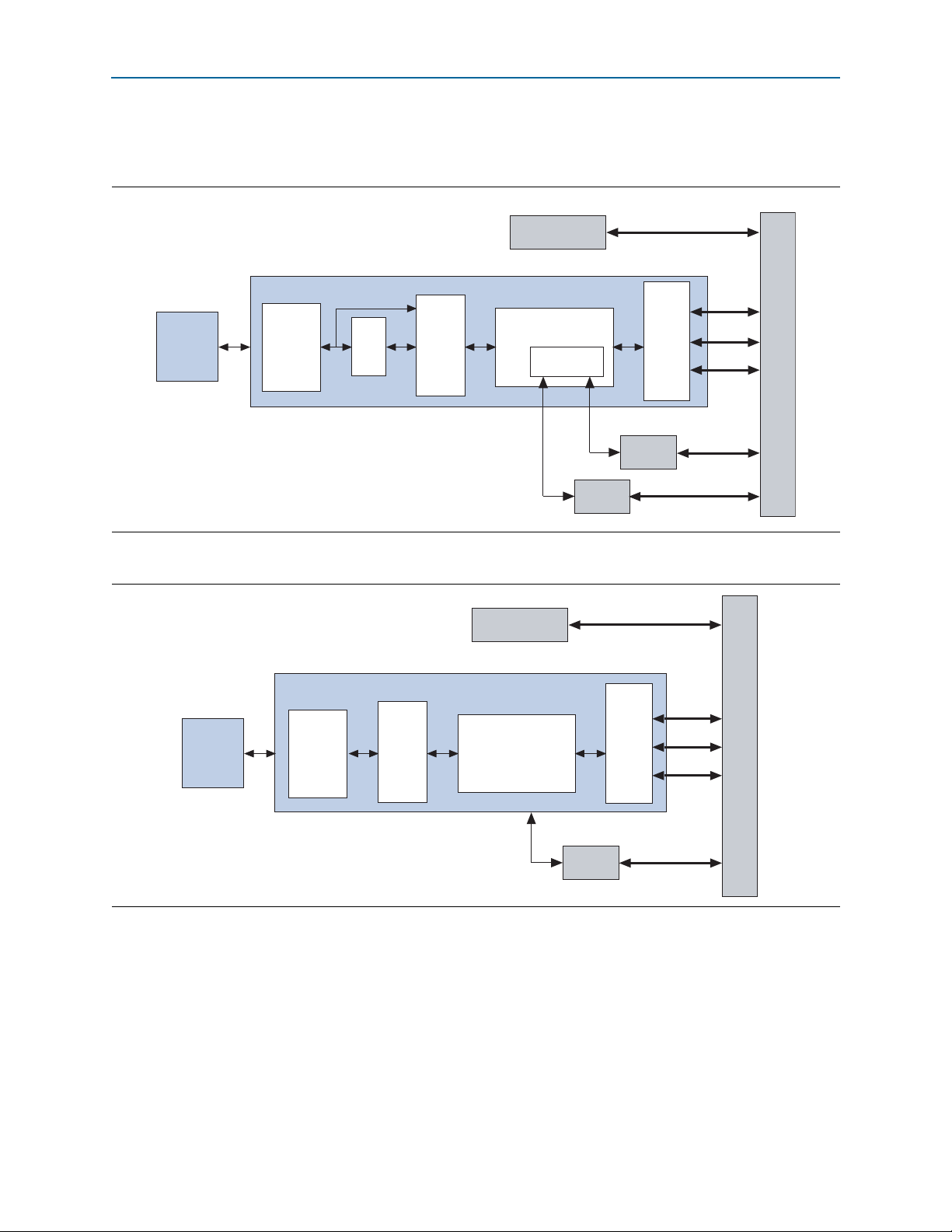
4–4 Chapter 4: IP Core Architecture
Clock
Domain
Crossing
(CDC)
Data
Link
Layer
(DLL)
Transaction Layer
(TL)
PHYMAC
IP Compiler for PCI Express Hard IP Implementation
Avalon-ST Rx
Avalon-ST Tx
Side Band
LMI
(Avalon-MM)
PCIe Reconfig
PIPE
Adapter
To Application Layer
LMI
Reconfig
Block
Clock & Reset
Selection
Transceiver
Configuration
Space
Application Interfaces
Figure 4–3 and Figure 4–4 illustrate the hard IP and soft IP implementations of the IP
Compiler for PCI Express with an Avalon-ST interface.
Figure 4–3. PCI Express Hard IP Implementation with Avalon-ST Interface to User Application
Figure 4–4. PCI Express Soft IP Implementation with Avalon-ST Interface to User Application
Transceiver
PIPE
Clock & Reset
IP Compiler for PCI Express Soft IP Implementation
Data
PHYMAC
Link
Layer
(DLL)
Transaction Layer
Selection
(TL)
Test
Avalon-ST Rx
Avalon-ST Tx
Adapter
Test_in/Test_out
Side Band
To Application Layer
IP Compiler for PCI Express User Guide August 2014 Altera Corporation
Page 63

Chapter 4: IP Core Architecture 4–5
Application Interfaces
Tab le 4– 1 provides the application clock frequencies for the hard IP and soft IP
implementations. As this table indicates, the Avalon-ST interface can be either 64 or
128 bits for the hard IP implementation. For the soft IP implementation, the Avalon-ST
interface is 64 bits.
Table 4–1. Application Clock Frequencies
Hard IP Implementation— Stratix IV GX and Hardcopy IV GX Devices
Lanes Gen1 Gen2
×1 62.5 MHz @ 64 bits (1) or 125 MHz @ 64 bits 125 MHz @ 64 bits
×4 125 MHz @ 64 bits
250 MHz @ 64 bits or
125 MHz @ 128 bits
×8 250 MHz @ 64 bits or 125 MHz @ 128 bits 250 MHz @ 128 bits
Hard IP Implementation—Arria II GX Devices
Lanes Gen1 Gen2
×1 62.5 MHz @ 64 bits (1) or 125 MHz @ 64 bits —
×4 125 MHz @ 64 bits —
×8 125 MHz @ 128 bits —
Hard IP Implementation—Arria II GZ Devices
Lanes Gen1 Gen2
×1 62.5 MHz @ 64 bits (1) or 125 MHz @ 64 bits 125 MHz @ 64 bits
×4 125 MHz @ 64 bits 125 MHz @ 128 bits
×8 125 MHz @ 128 bits —
Hard IP Implementation—Cyclone IV GX Devices
Lanes Gen1 Gen2
×1 62.5 MHz @ 64 bits or 125 MHz @ 64 bits —
×2 125 MHz @ 64 bits —
×4 125 MHz @ 64 bits —
Soft IP Implementation
Lanes Gen1 Gen2
×1 62.5 MHz @ 64 bits or125 MHz @64 bits —
×4 125 MHz @ 64 bits —
×8 250 MHz @ 64 bits —
Notes to Table 4–1:
(1) The 62.5 MHz application clock is available in parameter editor-generated Gen1:×1 hard IP implementations in any
device.
The following sections introduce the functionality of the interfaces shown in
Figure 4–3 and Figure 4–4. For more detailed information, refer to
Avalon-ST RX Port” on page 5–6
August 2014 Altera Corporation IP Compiler for PCI Express User Guide
and “64- or 128-Bit Avalon-ST TX Port” on page 5–15.
“64- or 128-Bit
Page 64

4–6 Chapter 4: IP Core Architecture
Application Interfaces
RX Datapath
The RX datapath transports data from the transaction layer to the Avalon-ST interface.
A FIFO buffers the RX data from the transaction layer until the streaming interface
accepts it. The adapter autonomously acknowledges all packets it receives from the
PCI Express IP core. The
rx_abort
and
rx_retry
signals of the transaction layer
interface are not used. Masking of non-posted requests is partially supported. Refer to
the description of the
rx_st_mask
<n> signal for further information about masking.
TX Datapath
The TX datapath transports data from the application's Avalon-ST interface to the
transaction layer. In the hard IP implementation, a FIFO buffers the Avalon-ST data
until the transaction layer accepts it.
If required, TLP ordering should be implemented by the application layer. The TX
datapath provides a TX credit (
available. For non–posted requests, this vector accounts for credits pending in the
Avalon-ST adapter. For example, if the
credits available to it. For completions and posted requests, the
the credits available in the transaction layer of the IP Compiler for PCI Express. For
example, for completions and posted requests, if
credits available to the application is (5 – <the number of credits in the adaptor>). You
must account for completion and posted credits which may be pending in the
Avalon-ST adapter. You can use the read and write FIFO pointers and the FIFO empty
flag to track packets as they are popped from the adaptor FIFO and transferred to the
transaction layer.
tx_cred
) vector which reflects the number of credits
tx_cred
value is 5, the application layer has 5
tx_cred
tx_cred
is 5, the actual number of
vector reflects
TLP Reordering
Applications that use the non-posted
more packets than
tx_cred
allows. While the IP core always obeys PCI Express flow
control rules, the behavior of the
is violated. When evaluating
tx_cred
that are in flight, and not yet reflected in
tx_cred
tx_cred
signal must ensure they never send
signal itself is unspecified if the credit limit
, the application must take into account TLPs
tx_cred
. Altera recommends your
application implement the following procedure, beginning from a state in which the
application has not yet issued any TLPs:
1. For calibration, ensure this application has issued no TLPs.
2. Wait for
3. Send as many TLPs as are allowed by
tx_cred
to indicate that credits are available.
tx_cred
. For example, if
tx_cred
indicates 3
credits of non-posted headers are available, the application sends 3 non-posted
TLPs, then stops.
In this step, the application exhausts
tx_cred
before waiting for more credits to
free. This step is required.
4. Wait for the TLPs to cross the Avalon-ST TX interface.
5. Wait at least 3 more clock cycles for
tx_cred
to reflect the consumed credits.
6. Repeat from Step 2.
IP Compiler for PCI Express User Guide August 2014 Altera Corporation
Page 65

Chapter 4: IP Core Architecture 4–7
Application Interfaces
1 The value of the non-posted
credits available. The non-posted credits displayed may be less than what is actually
available to the IP core.
LMI Interface (Hard IP Only)
The LMI bus provides access to the PCI Express configuration space in the transaction
layer. For more LMI details, refer to the “LMI Signals—Hard IP Implementation” on
page 5–37.
PCI Express Reconfiguration Block Interface (Hard IP Only)
The PCI Express reconfiguration bus allows you to dynamically change the read-only
values stored in the configuration registers. For detailed information refer to the “IP
Core Reconfiguration Block Signals—Hard IP Implementation” on page 5–38.
MSI (Message Signal Interrupt) Datapath
The MSI datapath contains the MSI boundary registers for incremental compilation.
The interface uses the transaction layer's request–acknowledge handshaking protocol.
You use the TX FIFO empty flag from the TX datapath FIFO for TX/MSI
synchronization. When the TX block application drives a packet to the Avalon-ST
adapter, the packet remains in the TX datapath FIFO as long as the IP core throttles
this interface. When you must send an MSI request after a specific TX packet, you can
use the TX FIFO empty flag to determine when the IP core receives the TX packet.
tx_cred
represents that there are at least that number of
For example, you may want to send an MSI request only after all TX packets are
issued to the transaction layer. Alternatively, if you cannot interrupt traffic flow to
synchronize the MSI, you can use a counter to count 16 writes (the depth of the FIFO)
after a TX packet has been written to the FIFO (or until the FIFO becomes empty) to
ensure that the transaction layer interface receives the packet, before you issue the
MSI request.
August 2014 Altera Corporation IP Compiler for PCI Express User Guide
Page 66

4–8 Chapter 4: IP Core Architecture
FIFO
Buffer
tx_st_data 0
app_msi_req
Non-Posted Credits
To Transaction
Layer
To Application
Layer
tx_cred0 for Completion
and Posted Requests
(from Transaction Layter)
tx_cred0 for
Non-Posted Requests
tx_fifo_empty0
tx_fifo_wrptr0
tx_fifo_rdptr0
Registers
Application Interfaces
Figure 4–5 illustrates the Avalon-ST TX and MSI datapaths.
Figure 4–5. Avalon-ST TX and MSI Datapaths
Incremental Compilation
The IP core with Avalon-ST interface includes a fully registered interface between the
user application and the PCI Express transaction layer. For the soft IP implementation,
you can use incremental compilation to lock down the placement and routing of the
IP Compiler for PCI Express with the Avalon-ST interface to preserve placement and
timing while changes are made to your application.
1 Incremental recompilation is not necessary for the PCI Express hard IP
implementation. This implementation is fixed. All signals in the hard IP
implementation are fully registered.
Avalon-MM Interface
IP Compiler for PCI Express variations generated in the Qsys design flow are PCI
Express Avalon-MM bridges: PCI Express endpoints with an Avalon-MM interface to
the application layer. The hard IP implementation of the PHYMAC and data link
layers communicates with a soft IP implementation of the transaction layer optimized
for the Avalon-MM protocol.
IP Compiler for PCI Express User Guide August 2014 Altera Corporation
Page 67

Chapter 4: IP Core Architecture 4–9
Tx
Rx
Transaction Layer Data Link Layer Physical Layer
IP Compiler for PCI Express
To Application Layer To Link
Avalon-MM
Master Port
IP Compiler for PCI Express
Avalon-MM Interface
Avalon-MM
Slave Port
(Control Register
Access)
Avalon-MM
Slave Port
Qsys component
controls the upstream
PCI Express devices.
Qsys component
controls access to
internal control and
status registers.
Root port controls the
downstream Qsys
component.
With information sent
by the application
layer, the transaction
layer generates a TLP,
which includes a
header and, optionally,
a data payload.
The data link layer
ensures packet
integrity, and adds a
sequence number and
link cyclic redundancy
code (LCRC) check to
the packet.
The physical layer
encodes the packet
and transmits it to the
receiving device on the
other side of the link.
The transaction layer
disassembles the
transaction and
transfers data to the
application layer in a
form that it recognizes.
The data link layer
verifies the packet's
sequence number and
checks for errors.
The physical layer
decodes the packet
and transfers it to the
data link layer.
Transaction Layer
Figure 4–6 shows the block diagram of an IP Compiler for PCI Express with an
Avalon-MM interface.
Figure 4–6. IP Compiler for PCI Express with Avalon-MM Interface
The PCI Express Avalon-MM bridge provides an interface between the PCI Express
transaction layer and other components across the system interconnect fabric.
Transaction Layer
The transaction layer sits between the application layer and the data link layer. It
generates and receives transaction layer packets. Figure 4–7 illustrates the transaction
layer of a component with two initialized virtual channels (VCs). The transaction
layer contains three general subblocks: the transmit datapath, the configuration space,
and the receive datapath, which are shown with vertical braces in Figure 4–7.
1 You can parameterize the Stratix IV GX IP core to include one or two virtual channels.
The Arria II GX and Cyclone IV GX implementations include a single virtual channel.
Tracing a transaction through the receive datapath includes the following steps:
1. The transaction layer receives a TLP from the data link layer.
2. The configuration space determines whether the transaction layer packet is well
formed and directs the packet to the appropriate virtual channel based on traffic
class (TC)/virtual channel (VC) mapping.
3. Within each virtual channel, transaction layer packets are stored in a specific part
of the receive buffer depending on the type of transaction (posted, non-posted, or
completion transaction).
August 2014 Altera Corporation IP Compiler for PCI Express User Guide
4. The transaction layer packet FIFO block stores the address of the buffered
transaction layer packet.
Page 68

4–10 Chapter 4: IP Core Architecture
n
Transaction Layer
5. The receive sequencing and reordering block shuffles the order of waiting
transaction layer packets as needed, fetches the address of the priority transaction
layer packet from the transaction layer packet FIFO block, and initiates the transfer
of the transaction layer packet to the application layer.
Figure 4–7. Architecture of the Transaction Layer: Dedicated Receive Buffer per Virtual Channel
Towards Data Link LayerTowards Application Layer
Interface Established per Virtual Channel Interface Established per Component
Virtual Channel 1
Tx1 Data
Tx1 Descriptor
Tx Transaction Layer
Packet Description
Tx1 Control
Virtual Channel 0
Tx0 Data
Tx0 Descriptor
Tx0 Control
Tx1 Request
Sequencing
Tx0 Request
Sequencing
Flow Control
Check & Reordering
Flow Control
Check & Reordering
& Data
Rx Flow
Control Credits
Virtual Channel
Arbitration & Tx
Sequencing
Transmit
Data Path
Virtual Channel 0
Rx0 Data
Rx0 Descriptor
Rx0 Control
& Status
Virtual Channel 1
Rx1 Data
Rx1 Descriptor
Rx1 Control
& Status
Type 0 Configuration Space
Rx0 Sequencing
& Reordering
Rx1 Sequencing
& Reordering
Receive Buffer
Posted & Completion
Non-Posted
Transaction Layer
Packet FIFO
Flow Control Update
Receive Buffer
Posted & Completion
Non-Posted
Transaction Layer
Packet FIFO
Flow Control Update
Tx Flow
Control Credits
Rx Transaction
Layer Packet
Configuratio
Space
Receive
Data Path
IP Compiler for PCI Express User Guide August 2014 Altera Corporation
Page 69

Chapter 4: IP Core Architecture 4–11
Transaction Layer
Tracing a transaction through the transmit datapath involves the following steps:
1. The IP core informs the application layer that sufficient flow control credits exist
for a particular type of transaction. The IP core uses
implementation and
tx_cred[35:0]
for the hard IP implementation. The
tx_cred[21:0]
for the soft IP
application layer may choose to ignore this information.
2. The application layer requests a transaction layer packet transmission. The
application layer must provide the PCI Express transaction and must be prepared
to provide the entire data payload in consecutive cycles.
3. The IP core verifies that sufficient flow control credits exist, and acknowledges or
postpones the request.
4. The application layer forwards the transaction layer packet. The transaction layer
arbitrates among virtual channels, and then forwards the priority transaction layer
packet to the data link layer.
Transmit Virtual Channel Arbitration
For Stratix IV GX devices, the IP Compiler for PCI Express allows you to specify a
high and low priority virtual channel as specified in Chapter 6 of the PCI Express Base
Specification 1.0a, 1.1, or 2.0. You can use the settings on the Buffer Setup page,
accessible from the Parameter Settings tab, to specify the number of virtual channels.
Refer to “Buffer Setup Parameters” on page 3–16.
Configuration Space
The configuration space implements the following configuration registers and
associated functions:
■ Header Type 0 Configuration Space for Endpoints
■ Header Type 1 Configuration Space for Root Ports
■ PCI Power Management Capability Structure
■ Message Signaled Interrupt (MSI) Capability Structure
■ Message Signaled Interrupt–X (MSI–X) Capability Structure
■ PCI Express Capability Structure
■ Virtual Channel Capabilities
The configuration space also generates all messages (PME#, INT, error, slot power
limit), MSI requests, and completion packets from configuration requests that flow in
the direction of the root complex, except slot power limit messages, which are
generated by a downstream port in the direction of the PCI Express link. All such
transactions are dependent upon the content of the PCI Express configuration space
as described in the PCI Express Base Specification 1.0a, 1.1, or 2.0.
f Refer To “Configuration Space Register Content” on page 6–1 or Chapter 7 in the PCI
Express Base Specification 1.0a, 1.1, or 2.0 for the complete content of these registers.
August 2014 Altera Corporation IP Compiler for PCI Express User Guide
Page 70

4–12 Chapter 4: IP Core Architecture
To Transaction Layer
Tx Transaction Layer
Packet Description & Data
Transaction Layer
Packet Generator
Retry Buffer
To Physical Layer
Tx Packets
Ack/Nack
Packets
Receive
Data Path
Transmit
Data Path
Rx Packets
DLLP
Checker
Transaction Layer
Packet Checker
DLLP
Generator
Tx Arbitration
Data Link Control
& Management
State Machine
Control
& Status
Configuration Space
Tx Flow Control Credits
Rx Flow Control Credits
Rx Transation Layer
Packet Description & Data
Power
Management
Function
Data Link Layer
Data Link Layer
The data link layer is located between the transaction layer and the physical layer. It is
responsible for maintaining packet integrity and for communication (by data link
layer packet transmission) at the PCI Express link level (as opposed to component
communication by transaction layer packet transmission in the interconnect fabric).
The data link layer is responsible for the following functions:
■ Link management through the reception and transmission of data link layer
packets, which are used for the following functions:
■ To initialize and update flow control credits for each virtual channel
■ For power management of data link layer packet reception and transmission
■ Data integrity through generation and checking of CRCs for transaction layer
■ Transaction layer packet retransmission in case of
■ Management of the retry buffer
■ Link retraining requests in case of error through the LTSSM of the physical layer
Figure 4–8 illustrates the architecture of the data link layer.
Figure 4–8. Data Link Layer
■ To tr a nsm it an d rec eive
ACK/NACK
packets and data link layer packets
reception using the retry buffer
packets
NAK
data link layer packet
IP Compiler for PCI Express User Guide August 2014 Altera Corporation
Page 71

Chapter 4: IP Core Architecture 4–13
Data Link Layer
The data link layer has the following subblocks:
■ Data Link Control and Management State Machine—This state machine is
synchronized with the physical layer’s LTSSM state machine and is also connected
to the configuration space registers. It initializes the link and virtual channel flow
control credits and reports status to the configuration space. (Virtual channel 0 is
initialized by default, as is a second virtual channel if it has been physically
enabled and the software permits it.)
■ Power Management—This function handles the handshake to enter low power
mode. Such a transition is based on register values in the configuration space and
received PM DLLPs.
■ Data Link Layer Packet Generator and Checker—This block is associated with the
data link layer packet’s 16-bit CRC and maintains the integrity of transmitted
packets.
■ Transaction Layer Packet Generator—This block generates transmit packets,
generating a sequence number and a 32-bit CRC. The packets are also sent to the
retry buffer for internal storage. In retry mode, the transaction layer packet
generator receives the packets from the retry buffer and generates the CRC for the
transmit packet.
■ Retry Buffer—The retry buffer stores transaction layer packets and retransmits all
unacknowledged packets in the case of NAK DLLP reception. For ACK DLLP
reception, the retry buffer discards all acknowledged packets.
■ ACK/NAK Packets—The ACK/NAK block handles ACK/NAK data link layer
packets and generates the sequence number of transmitted packets.
■ Transaction Layer Packet Checker—This block checks the integrity of the received
transaction layer packet and generates a request for transmission of an ACK/NAK
data link layer packet.
■ TX Arbitration—This block arbitrates transactions, basing priority on the
following order:
1. Initialize FC data link layer packet
2. ACK/NAK data link layer packet (high priority)
3. Update FC data link layer packet (high priority)
4. PM data link layer packet
5. Retry buffer transaction layer packet
6. Transaction layer packet
7. Update FC data link layer packet (low priority)
8. ACK/NAK FC data link layer packet (low priority)
August 2014 Altera Corporation IP Compiler for PCI Express User Guide
Page 72

4–14 Chapter 4: IP Core Architecture
Physical Layer
Physical Layer
The physical layer is the lowest level of the IP core. It is the layer closest to the link. It
encodes and transmits packets across a link and accepts and decodes received
packets. The physical layer connects to the link through a high-speed SERDES
interface running at 2.5 Gbps for Gen1 implementations and at 2.5 or 5.0 Gbps for
Gen2 implementations. Only the hard IP implementation supports the Gen2 rate of
5.0 Gbps.
The physical layer is responsible for the following actions:
■ Initializing the link
■ Scrambling and descrambling and 8B/10B encoding and decoding of 2.5 Gbps
(Gen1) or 5.0 Gbps (Gen2) per lane 8B/10B
■ Serializing and deserializing data
The hard IP implementation includes the following additional functionality:
■ PIPE 2.0 Interface Gen1/Gen2: 8-bit@250/500 MHz (fixed width, variable clock)
■ Auto speed negotiation (Gen2)
■ Training sequence transmission and decode
■ Hardware autonomous speed control
■ Auto lane reversal
IP Compiler for PCI Express User Guide August 2014 Altera Corporation
Page 73
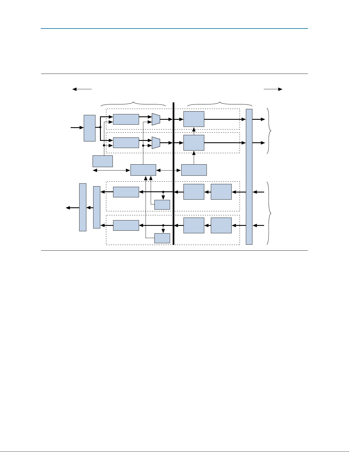
Chapter 4: IP Core Architecture 4–15
Scrambler
8B10B
Encoder
Lane n
Tx+ / Tx-
Scrambler
8B10B
Encoder
Lane 0
Tx+ / Tx-
Descrambler
8B10B
Decoder
Lane n
Rx+ / Rx-
Elastic
Buffer
LTSSM
State Machine
SKIP
Generation
Control & Status
PIPE
Emulation Logic
Link Serializer
for an x8 Link
Tx Packets
Rx MAC
Lane
Device Transceiver (per Lane) with 2.5 or 5.0 Gbps SERDES & PLL
Descrambler
8B10B
Decoder
Lane 0
Rx+ / Rx-
Elastic
Buffer
Rx MAC
Lane
PIPE
Interface
Multilane Deskew
Link Serializer for an x8 Link
Rx Packets
Transmit
Data Path
Receive
Data Path
MAC Layer PHY layer
To LinkTo Data Link Layer
Physical Layer
Physical Layer Architecture
Figure 4–9 illustrates the physical layer architecture.
Figure 4–9. Physical Layer
The physical layer is subdivided by the PIPE Interface Specification into two layers
(bracketed horizontally in Figure 4–9):
■ Media Access Controller (MAC) Layer—The MAC layer includes the Link
Training and Status state machine (LTSSM) and the scrambling/descrambling and
multilane deskew functions.
■ PHY Layer—The PHY layer includes the 8B/10B encode/decode functions, elastic
buffering, and serialization/deserialization functions.
The physical layer integrates both digital and analog elements. Intel designed the
PIPE interface to separate the MAC from the PHY. The IP core is compliant with the
PIPE interface, allowing integration with other PIPE-compliant external PHY devices.
Depending on the parameters you set in the parameter editor, the IP core can
automatically instantiate a complete PHY layer when targeting an Arria II GX, Arria
II GZ, Cyclone IV GX, HardCopy IV GX, Stratix II GX, or Stratix IV GX device.
August 2014 Altera Corporation IP Compiler for PCI Express User Guide
Page 74

4–16 Chapter 4: IP Core Architecture
Physical Layer
The PHYMAC block is divided in four main sub-blocks:
■ MAC Lane—Both the receive and the transmit path use this block.
■ On the receive side, the block decodes the physical layer packet (PLP) and
reports to the LTSSM the type of TS1/TS2 received and the number of TS1s
received since the LTSSM entered the current state. The LTSSM also reports the
reception of FTS, SKIP and IDL ordered sets and the reception of eight
consecutive D0.0 symbols.
■ On the transmit side, the block multiplexes data from the data link layer and
the LTSTX sub-block. It also adds lane specific information, including the lane
number and the force PAD value when the LTSSM disables the lane during
initialization.
■ LTSSM—This block implements the LTSSM and logic that tracks what is received
and transmitted on each lane.
■ For transmission, it interacts with each MAC lane sub-block and with the
LTSTX sub-block by asserting both global and per-lane control bits to generate
specific physical layer packets.
■ On the receive path, it receives the PLPs reported by each MAC lane sub-block.
It also enables the multilane deskew block and the delay required before the TX
alignment sub-block can move to the recovery or low power state. A higher
layer can direct this block to move to the recovery, disable, hot reset or low
power states through a simple request/acknowledge protocol. This block
reports the physical layer status to higher layers.
■ LTSTX (Ordered Set and SKP Generation)—This sub-block generates the physical
layer packet (PLP). It receives control signals from the LTSSM block and generates
PLP for each lane of the core. It generates the same PLP for all lanes and PAD
symbols for the link or lane number in the corresponding TS1/TS2 fields.
The block also handles the receiver detection operation to the PCS sub-layer by
asserting predefined PIPE signals and waiting for the result. It also generates a
SKIP ordered set at every predefined timeslot and interacts with the TX alignment
block to prevent the insertion of a SKIP ordered set in the middle of packet.
■ Deskew—This sub-block performs the multilane deskew function and the RX
alignment between the number of initialized lanes and the 64-bit data path.
The multilane deskew implements an eight-word FIFO for each lane to store
symbols. Each symbol includes eight data bits and one control bit. The FTS, COM,
and SKP symbols are discarded by the FIFO; the PAD and IDL are replaced by
D0.0 data. When all eight FIFOs contain data, a read can occur.
When the multilane lane deskew block is first enabled, each FIFO begins writing
after the first COM is detected. If all lanes have not detected a COM symbol after 7
clock cycles, they are reset and the resynchronization process restarts, or else the
RX alignment function recreates a 64-bit data word which is sent to the data link
layer.
IP Compiler for PCI Express User Guide August 2014 Altera Corporation
Page 75

Chapter 4: IP Core Architecture 4–17
PCI Express Avalon-MM Bridge
Reverse Parallel Loopback
In Arria II GX, Arria II GZ, Cyclone IV GX, and Stratix IV GX devices, the IP
Compiler for PCI Express hard IP implementation supports a reverse parallel
loopback path you can use to test the IP Compiler for PCI Express endpoint link
implementation from a PCI Express root complex. When this path is enabled, data
that the IP Compiler for PCI Express endpoint receives on the PCI Express link passes
through the RX PMA and the word aligner and rate matching FIFO buffer in the RX
PCS as usual. From the rate matching FIFO buffer, it passes along both of the
following two paths:
■ The usual data path through the IP Compiler for PCI Express hard IP block.
■ A reverse parallel loopback path to the TX PMA block and out to the PCI Express
link. The input path to the TX PMA is gated by a multiplexor that controls whether
the TX PMA receives data from the TX PCS or from the reverse parallel loopback
path.
f For information about the reverse parallel loopback mode and an illustrative block
diagram, refer to “PCIe (Reverse Parallel Loopback)” in the Transceiver Architecture in
Arria II Devices chapter of the Arria II Device Handbook, “Reverse Parallel Loopback” in
the Cyclone IV Transceivers Architecture chapter of the Cyclone IV Device Handbook, or
“PCIe Reverse Parallel Loopback” in the Transceiver Architecture in Stratix IV Devices
chapter of the Stratix IV Device Handbook.
For information about configuring and using the reverse parallel loopback path for
testing, refer to “Link and Transceiver Testing” on page 17–3.
PCI Express Avalon-MM Bridge
The IP Compiler for PCI Express uses the IP Compiler for PCI Express Avalon-MM
bridge module to connect the PCI Express link to the system interconnect fabric. The
bridge facilitates the design of PCI Express endpoints that include Qsys components.
The full-featured PCI Express Avalon-MM bridge provides three possible Avalon-MM
ports: a bursting master, an optional bursting slave, and an optional non-bursting
slave. The PCI Express Avalon-MM bridge comprises the following three modules:
■ TX Slave Module—This optional 64-bit bursting, Avalon-MM dynamic addressing
slave port propagates read and write requests of up to 4 KBytes in size from the
system interconnect fabric to the PCI Express link. The bridge translates requests
from the interconnect fabric to PCI Express request packets.
■ RX Master Module—This 64-bit bursting Avalon-MM master port propagates PCI
Express requests, converting them to bursting read or write requests to the system
interconnect fabric.
■ Control Register Access (CRA) Slave Module—This optional, 32-bit Avalon-MM
dynamic addressing slave port provides access to internal control and status
registers from upstream PCI Express devices and external Avalon-MM masters.
Implementations that use MSI or dynamic address translation require this port.
August 2014 Altera Corporation IP Compiler for PCI Express User Guide
Page 76

4–18 Chapter 4: IP Core Architecture
PCI Express Avalon-MM Bridge
Figure 4–10 shows the block diagram of a full-featured PCI Express Avalon-MM
bridge.
Figure 4–10. PCI Express Avalon-MM Bridge
PCI Express MegaCore Function
PCI Express Avalon-MM Bridge
Avalon Clock Domain PCI Express Clock Domain
Control Register
Access Slave
Address
Translator
Avalon-MM
Tx Slave
Avalon-MM
Tx Read
Response
System Interconnect Fabric
Address
Translator
Control & Status
Reg (CSR)
Clock
Domain
Crossing
Sync
Clock Domain
Boundary
MSI or
Legacy Interrupt
Generator
CRA Slave Module
PCI Express
Tx Controller
Tx Slave Module
PCI Link
Physical Layer
Data Link Layer
Transaction Layer
Avalon-MM
Rx Master
Avalon-MM
Rx Read
Response
Clock
Domain
Crossing
PCI Express
Rx Controller
Rx Master ModuleRx Master Module
The PCI Express Avalon-MM bridge supports the following TLPs:
■ Memory write requests
■ Received downstream memory read requests of up to 512 bytes in size
IP Compiler for PCI Express User Guide August 2014 Altera Corporation
Page 77

Chapter 4: IP Core Architecture 4–19
PCI Express Avalon-MM Bridge
■ Transmitted upstream memory read requests of up to 256 bytes in size
■ Completions
1 The PCI Express Avalon-MM bridge supports native PCI Express endpoints, but not
legacy PCI Express endpoints. Therefore, the bridge does not support I/O space BARs
and I/O space requests cannot be generated.
The bridge has the following additional characteristics:
■ Type 0 and Type 1 vendor-defined incoming messages are discarded
■ Completion-to-a-flush request is generated, but not propagated to the system
interconnect fabric
Each PCI Express base address register (BAR) in the transaction layer maps to a
specific, fixed Avalon-MM address range. You can use separate BARs to map to
various Avalon-MM slaves connected to the RX Master port.
The following sections describe the following modes of operation:
■ Avalon-MM-to-PCI Express Write Requests
■ Avalon-MM-to-PCI Express Upstream Read Requests
■ PCI Express-to-Avalon-MM Read Completions
■ PCI Express-to-Avalon-MM Downstream Write Requests
■ PCI Express-to-Avalon-MM Downstream Read Requests
■ PCI Express-to-Avalon-MM Read Completions
■ Avalon-MM-to-PCI Express Address Translation
■ Generation of PCI Express Interrupts
■ Generation of Avalon-MM Interrupts
Avalon-MM-to-PCI Express Write Requests
A Qsys-generated PCI Express Avalon-MM bridge accepts Avalon-MM burst write
requests with a burst size of up to 512 bytes.
The PCI Express Avalon-MM bridge converts the write requests to one or more PCI
Express write packets with 32– or 64–bit addresses based on the address translation
configuration, the request address, and the maximum payload size.
The Avalon-MM write requests can start on any address in the range defined in the
PCI Express address table parameters. The bridge splits incoming burst writes that
cross a 4 KByte boundary into at least two separate PCI Express packets. The bridge
also considers the root complex requirement for maximum payload on the PCI
Express side by further segmenting the packets if needed.
The bridge requires Avalon-MM write requests with a burst count of greater than one
to adhere to the following byte enable rules:
■ The Avalon-MM byte enable must be asserted in the first qword of the burst.
■ All subsequent byte enables must be asserted until the deasserting byte enable.
■ The Avalon-MM byte enable may deassert, but only in the last qword of the burst.
August 2014 Altera Corporation IP Compiler for PCI Express User Guide
Page 78

4–20 Chapter 4: IP Core Architecture
1 To improve PCI Express throughput, Altera recommends using an Avalon-MM burst
master without any byte-enable restrictions.
PCI Express Avalon-MM Bridge
Avalon-MM-to-PCI Express Upstream Read Requests
The PCI Express Avalon-MM bridge converts read requests from the system
interconnect fabric to PCI Express read requests with 32-bit or 64-bit addresses based
on the address translation configuration, the request address, and the maximum read
size.
The Avalon-MM TX slave interface of a Qsys-generated PCI Express Avalon-MM
bridge can receive read requests with burst sizes of up to 512 bytes sent to any
address. However, the bridge limits read requests sent to the PCI Express link to a
maximum of 256 bytes. Additionally, the bridge must prevent each PCI Express read
request packet from crossing a 4 KByte address boundary. Therefore, the bridge may
split an Avalon-MM read request into multiple PCI Express read packets based on the
address and the size of the read request.
For Avalon-MM read requests with a burst count greater than one, all byte enables
must be asserted. There are no restrictions on byte enable for Avalon-MM read
requests with a burst count of one. An invalid Avalon-MM request can adversely
affect system functionality, resulting in a completion with abort status set. An
example of an invalid request is one with an incorrect address.
PCI Express-to-Avalon-MM Read Completions
The PCI Express Avalon-MM bridge returns read completion packets to the initiating
Avalon-MM master in the issuing order. The bridge supports multiple and
out-of-order completion packets.
PCI Express-to-Avalon-MM Downstream Write Requests
When the PCI Express Avalon-MM bridge receives PCI Express write requests, it
converts them to burst write requests before sending them to the system interconnect
fabric. The bridge translates the PCI Express address to the Avalon-MM address space
based on the BAR hit information and on address translation table values configured
during the IP core parameterization. Malformed write packets are dropped, and
therefore do not appear on the Avalon-MM interface.
For downstream write and read requests, if more than one byte enable is asserted, the
byte lanes must be adjacent. In addition, the byte enables must be aligned to the size
of the read or write request.
PCI Express-to-Avalon-MM Downstream Read Requests
The PCI Express Avalon-MM bridge sends PCI Express read packets to the system
interconnect fabric as burst reads with a maximum burst size of 512 bytes. The bridge
converts the PCI Express address to the Avalon-MM address space based on the BAR
hit information and address translation lookup table values. The address translation
lookup table values are user configurable. Unsupported read requests generate a
completer abort response.
1 IP Compiler for PCI Express variations using the Avalon-ST interface can handle burst
reads up to the specified Maximum Payload Size.
IP Compiler for PCI Express User Guide August 2014 Altera Corporation
Page 79

Chapter 4: IP Core Architecture 4–21
PCI Express Avalon-MM Bridge
As an example, Table 4–2 lists the byte enables for 32-bit data.
Table 4–2. Valid Byte Enable Configurations
Byte Enable Value Description
4’b1111 Write full 32 bits
4’b0011 Write the lower 2 bytes
4’b1100 Write the upper 2 bytes
4’b0001 Write byte 0 only
4’b0010 Write byte 1 only
4’b0100 Write byte 2 only
4’b1000 Write byte 3 only
In burst mode, the IP Compiler for PCI Express supports only byte enable values that
correspond to a contiguous data burst. For the 32-bit data width example, valid values
in the first data phase are 4’b1111, 4’b1100, and 4’b1000, and valid values in the final
data phase of the burst are 4’b1111, 4’b0011, and 4’b0001. Intermediate data phases in
the burst can only have byte enable value 4’b1111.
Avalon-MM-to-PCI Express Read Completions
The PCI Express Avalon-MM bridge converts read response data from the external
Avalon-MM slave to PCI Express completion packets and sends them to the
transaction layer.
A single read request may produce multiple completion packets based on the
Maximum Payload Size and the size of the received read request. For example, if the
read is 512 bytes but the Maximum Payload Size 128 bytes, the bridge produces four
completion packets of 128 bytes each. The bridge does not generate out-of-order
completions. You can specify the Maximum Payload Size parameter on the Buffer
Setup page of the IP Compiler for PCI Express parameter editor. Refer to “Buffer
Setup Parameters” on page 3–16.
PCI Express-to-Avalon-MM Address Translation
The PCI Express address of a received request packet is translated to the Avalon-MM
address before the request is sent to the system interconnect fabric. This address
translation proceeds by replacing the MSB bits of the PCI Express address with the
value from a specific translation table entry; the LSB bits remain unchanged. The
number of MSB bits to replace is calculated from the total memory allocation of all
Avalon-MM slaves connected to the RX Master Module port. Six possible address
translation entries in the address translation table are configurable manually by Qsys.
Each entry corresponds to a PCI Express BAR. The BAR hit information from the
request header determines the entry that is used for address translation.
August 2014 Altera Corporation IP Compiler for PCI Express User Guide
Page 80

4–22 Chapter 4: IP Core Architecture
PCI Express Address
Inside IP Compiler for PCI Express
Matched BAR
selects Avalon-MM
address
Low address bits unchanged
(BAR-specific number of bits)
Hard-coded BAR-specific
Avalon-MM Addresses
Avalon-MM Address
BAR-specific Number of
High Avalon-MM Bits
Avalon Address B0
Avalon Address B1
Avalon Address B2
Avalon Address B3
Avalon Address B4
Avalon Address B5
M-1 N N-1 0P-1 N N-1 0
High Low LowHigh
BAR0 (or 0:1)
BAR1
BAR2
BAR3
BAR4
BAR5
PCI Express Avalon-MM Bridge
Figure 4–11 depicts the PCI Express Avalon-MM bridge address translation process.
Figure 4–11. PCI Express Avalon-MM Bridge Address Translation (Note 1)
Note to Figure 4–11:
(1) N is the number of pass-through bits (BAR specific). M is the number of Avalon-MM address bits. P is the number of PCI Express address bits
(32 or 64).
The Avalon-MM RX master module port has an 8-byte datapath. The Qsys
interconnect fabric does not support native addressing. Instead, it supports dynamic
bus sizing. In this method, the interconnect fabric handles mismatched port widths
transparently.
f For more information about both native addressing and dynamic bus sizing, refer to
the “Address Alignment” section in the “Avalon Memory-Mapped Interfaces”
chapter of the Avalon Interface Specifications.
Avalon-MM-to-PCI Express Address Translation
The Avalon-MM address of a received request on the TX Slave Module port is
translated to the PCI Express address before the request packet is sent to the
transaction layer. This address translation process proceeds by replacing the MSB bits
of the Avalon-MM address with the value from a specific translation table entry; the
LSB bits remain unchanged. The number of MSB bits to be replaced is calculated
based on the total address space of the upstream PCI Express devices that the IP
Compiler for PCI Express can access.
IP Compiler for PCI Express User Guide August 2014 Altera Corporation
The address translation table contains up to 512 possible address translation entries
that you can configure. Each entry corresponds to a base address of the PCI Express
memory segment of a specific size. The segment size of each entry must be identical.
The total size of all the memory segments is used to determine the number of address
MSB bits to be replaced. In addition, each entry has a 2-bit field,
Sp[1:0]
, that
Page 81

Chapter 4: IP Core Architecture 4–23
PCI Express Avalon-MM Bridge
specifies 32-bit or 64-bit PCI Express addressing for the translated address. Refer to
Figure 4–12 on page 4–24. The most significant bits of the Avalon-MM address are
used by the system interconnect fabric to select the slave port and are not available to
the slave. The next most significant bits of the Avalon-MM address index the address
translation entry to be used for the translation process of MSB replacement.
For example, if the core is configured with an address translation table with the
following attributes:
■ Number of Address Pages—16
■ Size of Address Pages—1MByte
■ PCI Express Address Size—64 bits
then the values in Figure 4–12 are:
■ N = 20 (due to the 1 MByte page size)
■ Q = 16 (number of pages)
■ M = 24 (20 + 4 bit page selection)
■ P = 64
In this case, the Avalon address is interpreted as follows:
■ Bits [31:24] select the TX slave module port from among other slaves connected to
the same master by the system interconnect fabric. The decode is based on the base
addresses assigned in Qsys.
■ Bits [23:20] select the address translation table entry.
■ Bits [63:20] of the address translation table entry become PCI Express address bits
[63:20].
■ Bits [19:0] are passed through and become PCI Express address bits [19:0].
The address translation table can be hardwired or dynamically configured at run
time. When the IP core is parameterized for dynamic address translation, the address
translation table is implemented in memory and can be accessed through the CRA
slave module. This access mode is useful in a typical PCI Express system where
address allocation occurs after BIOS initialization.
For more information about how to access the dynamic address translation table
through the control register access slave, refer to the “Avalon-MM-to-PCI Express
Address Translation Table” on page 6–9.
August 2014 Altera Corporation IP Compiler for PCI Express User Guide
Page 82
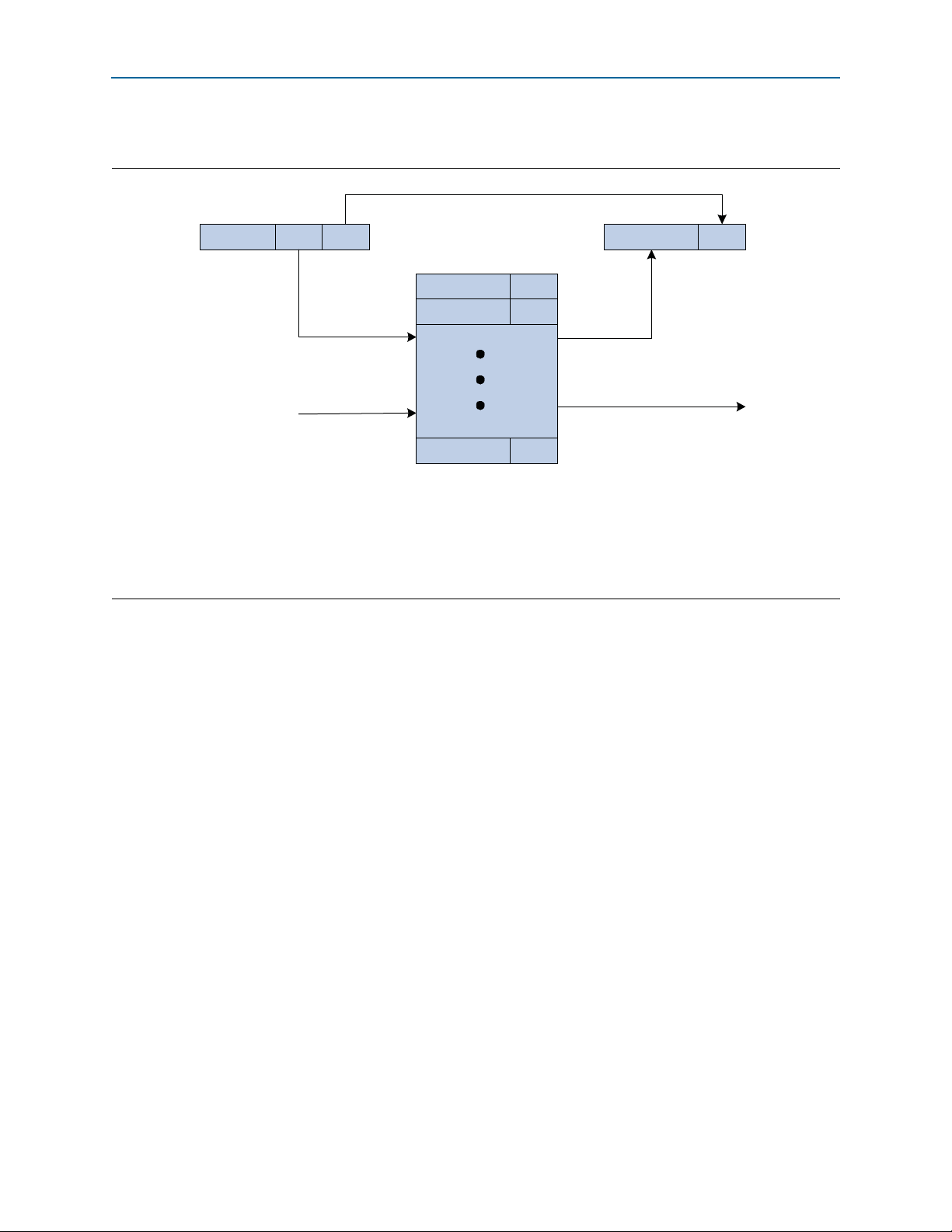
4–24 Chapter 4: IP Core Architecture
PCIe Address Q-1
SpQ-1
Space Indication
PCI Express address from Table Entry
becomes High PCI Express address bits
PCI Express Address
High
Low
P-1 N N-1 0
Low address bits unchanged
Avalon-MM-to-PCI Express
Address Translation Table
(Q entries by P-N bits wide)
PCIe Address 0 Sp0
PCIe Address 1 Sp1
Avalon-MM Address
High
Slave Base
Address
Low
M-131 M N N-1 0
Table updates from
control register port
High Avalon-MM Address
Bits Index table
PCI Express Avalon-MM Bridge
Figure 4–12 depicts the Avalon-MM-to-PCI Express address translation process.
Figure 4–12. Avalon-MM-to-PCI Express Address Translation (Note 1) (2) (3) (4) (5)
Notes to Figure 4–12:
(1) N is the number of pass-through bits.
(2) M is the number of Avalon-MM address bits.
(3) P is the number of PCI Express address bits.
(4) Q is the number of translation table entries.
(5) Sp[1:0] is the space indication for each entry.
Generation of PCI Express Interrupts
The PCI Express Avalon-MM bridge supports MSI or legacy interrupts. The completer
only, single dword variant includes an interrupt generation module. For other
variants with the Avalon-MM interface, interrupt support requires instantiation of the
CRA slave module where the interrupt registers and control logic are implemented.
The Qsys-generated PCI Express Avalon-MM bridge supports the Avalon-MM
individual requests interrupt scheme: multiple input signals indicate incoming
interrupt requests, and software must determine priorities for servicing simultaneous
interrupts the IP Compiler for PCI Express receives on the Avalon-MM interface.
In the Qsys-generated IP Compiler for PCI Express, the RX master module port has as
many as 16 Avalon-MM interrupt input signals (
Each interrupt signal indicates a distinct interrupt source. Assertion of any of these
signals, or a PCI Express mailbox register write access, sets a bit in the PCI Express
interrupt status register. Multiple bits can be set at the same time; software determines
priorities for servicing simultaneous incoming interrupt requests. Each set bit in the
PCI Express interrupt status register generates a PCI Express interrupt, if enabled,
when software determines its turn.
Software can enable the individual interrupts by writing to the IP Compiler for PCI
Express “Avalon-MM to PCI Express Interrupt Enable Register Address: 0x0050” on
page 6–8 through the CRA slave.
RXmirq_irq[
<n>
:0]
, where <n> ≤ 15)) .
IP Compiler for PCI Express User Guide August 2014 Altera Corporation
Page 83

Chapter 4: IP Core Architecture 4–25
PCI Express Avalon-MM Bridge
In Qsys-generated systems, when any interrupt input signal is asserted, the
corresponding bit is written in the “Avalon-MM to PCI Express Interrupt Status
Register Address: 0x0040” on page 6–7. Software reads this register and decides
priority on servicing requested interrupts.
After servicing the interrupt, software must clear the appropriate serviced interrupt
status
bit and ensure that no other interrupts are pending. For interrupts caused by
“Avalon-MM to PCI Express Interrupt Status Register Address: 0x0040” mailbox
writes, the status bits should be cleared in the “Avalon-MM to PCI Express Interrupt
Status Register Address: 0x0040”. For interrupts due to the incoming interrupt
signals on the Avalon-MM interface, the interrupt status should be cleared in the
Avalon-MM component that sourced the interrupt. This sequence prevents interrupt
requests from being lost during interrupt servicing.
Figure 4–13 shows the logic for the entire PCI Express interrupt generation process.
Figure 4–13. IP Compiler for PCI Express Avalon-MM Interrupt Propagation to the PCI Express Link
(Configuration Space Command Register [10])
Avalon-MM-to-PCI-Express
Interrupt Status and Interrupt
Enable Register Bits
A2P_MAILBOX_INT7
A2P_MB_IRQ7
A2P_MAILBOX_INT6
A2P_MB_IRQ6
A2P_MAILBOX_INT5
A2P_MB_IRQ5
A2P_MAILBOX_INT4
A2P_MB_IRQ4
A2P_MAILBOX_INT3
A2P_MB_IRQ3
A2P_MAILBOX_INT2
A2P_MB_IRQ2
A2P_MAILBOX_INT1
A2P_MB_IRQ1
A2P_MAILBOX_INT0
A2P_MB_IRQ0
AV_IRQ_ASSERTED
AVL_IRQ
Interrupt Disable
PCI Express Virtual INTA signalling
(When signal rises ASSERT_INTA Message Sent)
(When signal falls DEASSERT_INTA Message Sent)
SET
DQ
Q
CLR
MSI Request
(Configuration Space Message Control Register[0])
MSI Enable
The PCI Express Avalon-MM bridge selects either MSI or legacy interrupts
automatically based on the standard interrupt controls in the PCI Express
configuration space registers. The
Command
interrupts. The
register (at configuration space offset 0x4) can be used to disable legacy
MSI Enable
bit, which is bit 0 of the
Interrupt Disable
MSI Control Status
bit, which is bit 10 of the
register in the
MSI capability register (bit 16 at configuration space offset 0x50), can be used to
enable MSI interrupts.
August 2014 Altera Corporation IP Compiler for PCI Express User Guide
Page 84

4–26 Chapter 4: IP Core Architecture
Completer Only PCI Express Endpoint Single DWord
Only one type of interrupt can be enabled at a time. However, to change the selection
of MSI or legacy interrupts during operation, software must ensure that no interrupt
request is dropped. Therefore, software must first enable the new selection and then
disable the old selection. To set up legacy interrupts, software must first clear the
Interrupt Disable
software must first set the
bit and then clear the
MSI enable
bit and then set the
MSI enable
bit. To set up MSI interrupts,
Interrupt Disable
bit.
Generation of Avalon-MM Interrupts
Generation of Avalon-MM interrupts requires the instantiation of the CRA slave
module where the interrupt registers and control logic are implemented. The CRA
slave port has an Avalon-MM Interrupt (
A write access to an Avalon-MM mailbox register sets one of the
bits in the “PCI Express to Avalon-MM Interrupt Status Register Address: 0x3060”
on page 6–11 and asserts the
CraIrq_o
enable the interrupt by writing to the “PCI Express to Avalon-MM Interrupt Enable
Register Address: 0x3070” on page 6–11 through the CRA slave. After servicing the
interrupt, software must clear the appropriate serviced interrupt
PCI-Express-to-Avalon-MM
Interrupt Status
other interrupt pending.
CraIrq_irq
or
CraIrq_irq
in Qsys systems) output signal.
P2A_MAILBOX_INT
output, if enabled. Software can
status
bit in the
register and ensure that there is no
<n>
Completer Only PCI Express Endpoint Single DWord
The completer only single dword endpoint is intended for applications that use the
PCI Express protocol to perform simple read and write register accesses from a host
CPU. The completer only single dword endpoint is a hard IP implementation
available for Qsys systems, and includes an Avalon-MM interface to the application
layer. The Avalon-MM interface connection in this variation is 32 bits wide. This
endpoint is not pipelined; at any time a single request can be outstanding.
The completer-only single dword endpoint supports the following requests:
■ Read and write requests of a single dword (32 bits) from the root complex
■ Completion with completer abort status generation for other types of non-posted
requests
■ INTX or MSI support with one Avalon-MM interrupt source
As this figure illustrates, the IP Compiler for PCI Express links to a PCI Express root
complex. A bridge component in the IP Compiler for PCI Express includes IP
Compiler for PCI Express TX and RX blocks, an Avalon-MM RX master, and an
interrupt handler. The bridge connects to the FPGA fabric using an Avalon-MM
interface. The following sections provide an overview of each block in the bridge.
IP Compiler for PCI Express RX Block
The IP Compiler for PCI Express RX control logic interfaces to the hard IP block to
process requests from the root complex. It supports memory reads and writes of a
single dword. It generates a completion with Completer Abort (CA) status for reads
greater than four bytes and discards all write data without further action for write
requests greater than four bytes.
IP Compiler for PCI Express User Guide August 2014 Altera Corporation
Page 85

Chapter 4: IP Core Architecture 4–27
Completer Only PCI Express Endpoint Single DWord
The RX block passes header information to the Avalon-MM master, which generates
the corresponding transaction to the Avalon-MM interface. The bridge accepts no
additional requests while a request is being processed. While processing a read
request, the RX block deasserts the
ready
signal until the TX block sends the
corresponding completion packet to the hard IP block. While processing a write
request, the RX block sends the request to the Avalon-MM system interconnect fabric
before accepting the next request.
Avalon-MM RX Master Block
The 32-bit Avalon-MM master connects to the Avalon-MM system interconnect fabric.
It drives read and write requests to the connected Avalon-MM slaves, performing the
required address translation. The RX master supports all legal combinations of byte
enables for both read and write requests.
f For more information about legal combinations of byte enables, refer to Chapter 3,
Avalon Memory-Mapped Interfaces in the Avalon Interface Specifications.
IP Compiler for PCI Express TX Block
The TX block sends completion information to the IP Compiler for PCI Express hard
IP block. The IP core then sends this information to the root complex. The TX
completion block generates a completion packet with Completer Abort (CA) status
and no completion data for unsupported requests. The TX completion block also
supports the zero-length read (flush) command.
Interrupt Handler Block
The interrupt handler implements both INTX and MSI interrupts. The
in the configuration register specifies the interrupt type. The
of MSI message control portion in MSI Capability structure. It is bit[16] of 0x050 in the
configuration space registers. If the
IP Compiler for PCI Express when received, otherwise INTX is signaled. The interrupt
handler block supports a single interrupt source, so that software may assume the
source. You can disable interrupts by leaving the interrupt signal unconnected in the
interrupt signals unconnected in the IRQ column of Qsys. When the MSI registers in
the configuration space of the completer only single dword IP Compiler for PCI
Express are updated, there is a delay before this information is propagated to the
Bridge module. You must allow time for the Bridge module to update the MSI register
information. Under normal operation, initialization of the MSI registers should occur
substantially before any interrupt is generated. However, failure to wait until the
update completes may result in any of the following behaviors:
■ Sending a legacy interrupt instead of an MSI interrupt
msi_enable
msi_enable
msi_enable_bit
bit
is part
bit is on, an MSI request is sent to the
■ Sending an MSI interrupt instead of a legacy interrupt
■ Loss of an interrupt request
August 2014 Altera Corporation IP Compiler for PCI Express User Guide
Page 86

4–28 Chapter 4: IP Core Architecture
Completer Only PCI Express Endpoint Single DWord
IP Compiler for PCI Express User Guide August 2014 Altera Corporation
Page 87

August 2014
<edit Part Number variable in chapter>
This chapter describes the signals that are part of the IP Compiler for PCI Express for
each of the following primary configurations:
■ Signals in the Hard IP Implementation Root Port with Avalon-ST Interface Signals
■ Signals in the Hard IP Implementation Endpoint with Avalon-ST Interface
■ Signals in the Soft IP Implementation with Avalon-ST Interface
■ Signals in the Soft or Hard Full-Featured IP Core with Avalon-MM Interface
■ Signals in the Qsys Hard Full-Featured IP Core with Avalon-MM Interface
■ Signals in the Completer-Only, Single Dword, IP Core with Avalon-MM Interface
■ Signals in the Qsys Completer-Only, Single Dword, IP Core with Avalon-MM
1 Altera does not recommend the Descriptor/Data interface for new designs.
5. IP Core Interfaces
Interface
Avalon-ST Interface
The main functional differences between the hard IP and soft IP implementations
using an Avalon-ST interface are the configuration and clocking schemes. In addition,
the hard IP implementation offers a 128-bit Avalon-ST bus for some configurations. In
128-bit mode, the streaming interface clock,
core clock,
streaming interface clock,
and the streaming data width is 64 bits.
Figure 5–1, Figure 5–2, and Figure 5–3 illustrate the top-level signals for IP cores that
use the Avalon-ST interface.
core_clk
pld_clk
, is one-half the frequency of the
, and the streaming data width is 128 bits. In 64-bit mode, the
pld_clk
, is the same frequency as the core clock,
core_clk
,
August 2014 Altera Corporation IP Compiler for PCI Express User Guide
Page 88
rx_st_ready<n>
rx_st_valid<n>
rx_st_data<n>[63:0], [127:0]
rx_st_sop<n>
rx_st_eop<n>
rx_st_empty<n>
rx_st_err<n>
rx_st_mask<n>
rx_st_bardec<n>[7:0]
rx_st_be<n>[7:0], [15:0]
avs_pcie_reconfig_address[7:0]
avs_pcie_reconfig_byteenable[1:0]
avs_pcie_reconfig_chipselect
avs_pcie_reconfig_write
avs_pcie_reconfig_writedata[15:0]
avs_pcie_reconfig_waitrequest
avs_pcie_reconfig_read
avs_pcie_reconfig_readdata[15:0]
avs_pcie_reconfig_readdatavalid
avs_pcie_reconfig_clk
avs_pcie_reconfig_rstn
IP Compiler for PCI Express Hard IP Implementation
Test
Interface
Rx Port
(Path to
Virtual
Channel <n>)
tx_st_ready<n>
tx_st_valid<n>
tx_st_data<n>[63:0], [127:0]
tx_st_sop<n>
tx_st_eop<n>
tx_st_empty<n>
tx_st_err<n>
tx_fifo_full<n>
tx_fifo_empty<n>
tx_fifo_rdptr<n>[3:0]
tx_fifo_wrptr<n>[3:0]
tx_cred<n>[35:0]
nph_alloc_1cred_vc0
npd_alloc_1cred_vc0
npd_cred_vio_vc0
nph_cred_vio_vc0
Clocks
Power
Mnmt
Completion
Interface
Clocks -
Simulation
Only
Tx Port
(Path to
Virtual
Channell <n>)
Reconfiguration
Block
(optional)
Config
ECC Error
Interrupts
LMI
(1)
(2)
lmi_dout[31:0]
lmi_ack
lmi_addr[11:0]
lmi_din[31:0]
lmi_rden
pclk_in
clk250_out
clk500_out
lmi_wren
pipe_mode
rate_ext
txdata0_ext[7:0]
txdatak0_ext
txdetectrx0_ext
txelecidle0_ext
txcompl0_ext
rxpolarity0_ext
powerdown0_ext[1:0]
tx_pipemargin
tx_pipedeemph
rxdata0_ext[7:0]
rxdatak0_ext
rxvalid0_ext
phystatus0_ext
rxelecidle0_ext
rxstatus0_ext[2:0]
pipe_rstn
pipe_txclk
8-bit
PIPE
PIPE
Interface
Simulation
Only
test_out[63:0]
test_in[39:0]
lane_act[3:0]
rx_st_fifo_full<n>
rx_st_fifo_empty<n>
tl_cfg_add[3:0]
tl_cfg_ctl[31:0]
tl_cfg_ctl_wr
tl_cfg_sts[52:0]
tl_cfg_sts_wr
hpg_ctrler[4:0]
reconfig_fromgxb[<n>:0]
reconfig_togxb[<n>:0]
reconfig_clk
cal_blk_clk
fixedclk_serdes
busy_altgxb_reconfig
reset_reconfig_altgxb_reconfig
gxb_powerdown
Transceiver
Control
These signals are
internal for
<variant>_plus.v or .vhd)
for
internal
PHY
tx_out0
tx_out1
tx_out2
tx_out3
tx_out4
tx_out5
tx_out6
tx_out7
rx_in0
rx_in1
rx_in2
rx_in3
rx_in4
rx_in5
rx_in6
rx_in7
Serial
IF to
PIPE
Avalon-ST
Avalon-ST
Component
Specific
Component
Specific
derr_cor_ext_rcv[1:0]
derr_rpl
derr_cor_ext_rpl
r2c_err0
r2c_err1
aer_msi_num[4:0]
pex_msi_num[4:0]
int_status[4:0]
serr_out
pme_to_cr
pme_to_sr
pm_data
pm_auxpwr
cpl_err[6:0]
cpl_pending<n>
refclk
pld_clk
core_clk_out
pcie_rstn
local_rstn
suc_spd_neg
dl_ltssm[4:0]
npor
srst
crst
l2_exit
hotrst_exit
dlup_exit
reset_status
rc_pll_locked
Reset &
Link
Training
<variant>
<variant>_plus
5–2 Chapter 5: IP Core Interfaces
Figure 5–1. Signals in the Hard IP Implementation Root Port with Avalon-ST Interface Signals
Signals in the PCI Express Hard IP MegaCore Function
rx_st_ready0
rx_st_valid0
rx_st_data0[63..0], [127:0]
Avalon-ST
Rx Port
(Path to
Virtual
Channel 0)
Tx Port
(Path to
Virtual
Channel 0)
Notes to Figure 5–1:
(1) Available in Arria II GX, Arria II GZ, Cyclone IV GX,, and Stratix IV G devices. TFor Stratix IV GX devices, <n> = 16 for ×1 and ×4 IP cores and <n>
= 33 in the ×8 IP core.
(2) Available in Arria II GX, Arria II GZ, Cyclone IV GX, and Stratix IV GX devices. For Stratix IV GX
IP Compiler for PCI Express User Guide August 2014 Altera Corporation
Component
Specific
Avalon-ST
Component
Specific
Clocks
Reset
Interrupt
Power
Mnmt
Completion
Interface
Clocks -
Simulation
Only (2)
rx_st_sop0
rx_st_eop0
rx_st_empty
rx_st_err0
rx_st_mask0
rx_st_bardec0[7:0]
rx_st_be0[7:0], [15:0]
rx_fifo_full0
rx_fifo_empty0
tx_st_ready0
tx_st_valid0
tx_st_data0[63..0], [127:0]
tx_st_sop0
tx_st_eop0
tx_st_empty
tx_st_err0
tx_fifo_full0
tx_fifo_empty0
tx_fifo_rdptr0[3:0]
tx_fifo_wrptr0[3:0]
tx_cred0[35..0]
refclk
pld_clk
core_clk_out
npor
srst
crst
l2_exit
hotrst_exit
dlup_exit
app_msi_req
app_msi_ack
app_msi_tc [2:0]
app_msi_num [4:0]
pex_msi_num [4:0]
app_int_sts
app_int_ack
pme_to_cr
pme_to_sr
cpl_err [6:0]
cpl_pending0
pclk_in
clk250_out
clk500_out
(1)
(1)
(1)
reconfig_fromgxb[1:0]
reconfig_clk
reconfig_togxb[2:0]
cal_blk_clk
tx_out0
tx_out1
tx_out2
tx_out3
tx_out4
tx_out5
tx_out6
tx_out7
rx_in0
rx_in1
rx_in2
rx_in3
rx_in4
rx_in5
rx_in6
rx_in7
pipe_mode
rate_ext
txdata0_ext[7:0]
txdatak0_ext
txdetectrx0_ext
txelecidle0_ext
txcompl0_ext
rxpolarity0_ext
powerdown0_ext[1:0]
rxdata0_ext[7:0]
rxdatak0_ext
rxvalid0_ext
phystatus0_ext
rxelecidle0_ext
rxstatus0_ext[2:0]
tl_cfg_add[3:0]
tl_cfg_ctl[31:0]
tl_cfg_ctl_wr
tl_cfg_sts[52:0]
tl_cfg_sts_wr
lmi_dout[31:0]
lmi_rden
lmi_wren
lmi_ack
lmi_addr[11:0]
lmi_din[31:0]
test_out[64:0]
test_in[15:0]
reconfig_togxb
Transceiver
Control
Serial
IF to
PIPE
for
internal
PHY
Repeated for
8-bit
PIPE
Config
LMI
Test
Interface
, <n> = 3.
Lanes 1-7
Avalon-ST Interface
PIPE
Interface
Simulation
Only (2)
Page 89

Chapter 5: IP Core Interfaces 5–3
)
Avalon-ST Interface
Figure 5–2. Signals in the Hard IP Implementation Endpoint with Avalon-ST Interface
IP Compiler for PCI Express Hard IP Implementation
Rx Port
(Path to
Virtual
Channel
Tx Port
(Path to
Virtual
Channel
Reset &
Link
Training
Avalon-ST
)
<n>
Component
Specific
Avalon-ST
<n>
)
Component
Specific
Clocks
<variant>
<variant>
Reconfiguration
Block
(optional)
ECC Error
Interrupt
Power
Mnmt
Completion
Interface
_plus
rx_st_ready
rx_st_valid
rx_st_data
rx_st_sop
rx_st_eop
rx_st_empty
rx_st_err
rx_st_mask
rx_st_bardec
rx_st_be
tx_st_ready
tx_st_valid
tx_st_data
tx_st_sop
tx_st_eop
tx_st_empty
tx_st_err
tx_fifo_full
tx_fifo_empty
tx_fifo_rdptr
tx_fifo_wrptr
tx_cred
nph_alloc_1cred_vc0
npd_alloc_1cred_vc0
npd_cred_vio_vc0
nph_cred_vio_vc0
refclk
pld_clk
core_clk_out
pcie_rstn
local_rstn
suc_spd_neg
ltssm[4:0]
npor
srst
crst
l2_exit
hotrst_exit
dlup_exit
reset_status
rc_pll_locked
avs_pcie_reconfig_address[7:0]
avs_pcie_reconfig_byteenable[1:0]
avs_pcie_reconfig_chipselect
avs_pcie_reconfig_write
avs_pcie_reconfig_writedata[15:0]
avs_pcie_reconfig_waitrequest
avs_pcie_reconfig_read
avs_pcie_reconfig_readdata[15:0]
avs_pcie_reconfig_readdatavalid
avs_pcie_reconfig_clk
avs_pcie_reconfig_rstn
derr_cor_ext_rcv[1:0]
derr_rpl
derr_cor_ext_rpl
r2c_err0
r2c_err1
app_msi_req
app_msi_ack
app_msi_tc[2:0]
app_msi_num[4:0]
pex_msi_num[4:0]
app_int_sts
app_int_ack
pme_to_cr
pme_to_sr
pm_event
pm_data
pm_auxpwr
cpl_err[6:0]
cpl_pending
<n>
<n>
<n>
<n>
<n>
<n>
<n>
<n>
<n>
<n>
<n>
<n>
<n>
[35:0]
<n>
[63:0], [127:0]
<n>
<n>
<n>
[7:0]
[7:0], [15:0]
<n>
[63:0], [127:0]
<n>
<n>
<n>
[3:0]
<n>
[3:0]
<n>
reconfig_fromgxb[
(1)
reconfig_togxb[
(2)
fixedclk_serdes
busy_altgxb_reconfig
pll_powerdown
gxb_powerdown
txdata0_ext[7:0]
txdetectrx0_ext
txelecidle0_ext
rxpolarity0_ext
powerdown0_ext[1:0]
tx_pipedeemph
rxdata0_ext[7:0]
phystatus0_ext
rxelecidle0_ext
rxstatus0_ext[2:0]
tl_cfg_add[3:0]
tl_cfg_ctl[31:0]
tl_cfg_sts[52:0]
rx_st_fifo_full
rx_st_fifo_empty
<n>
<n>
reconfig_clk
cal_blk_clk
tx_out0
tx_out1
tx_out2
tx_out3
tx_out4
tx_out5
tx_out6
tx_out7
rx_in0
rx_in1
rx_in2
rx_in3
rx_in4
rx_in5
rx_in6
rx_in7
pipe_mode
rate_ext
txdatak0_ext
txcompl0_ext
tx_pipemargin
rxdatak0_ext
rxvalid0_ext
pipe_rstn
pipe_txclk
pclk_in
clk250_out
clk500_out
tl_cfg_ctl_wr
tl_cfg_sts_wr
hpg_ctrler
lmi_dout[31:0]
lmi_rden
lmi_wren
lmi_ack
lmi_addr[11:0]
lmi_din[31:0]
test_out[63:0]
test_in[39:0]
lane_act[3:0]
<n>
<n>
:0]
:0]
Transceiver
Control
These signals are
internal for
<variant>
_
plus.v or .vhd
Serial
IF to
PIPE
for
internal
PHY
8-bit
PIPE
Interface
Simulation
Clocks -
Simulation
Only
PIPE
Only (4)
Config
LMI
Test
Interface
Notes to Figure 5–2:
(1) Available in Stratix IV GX, devices. For Stratix IV GX devices, <n> = 16 for ×1 and ×4 IP cores and <n> = 33 in the ×8 IP core.
(2) Available in Stratix IV GX. For Stratix IV GX
reconfig_togxb
, <n> = 3.
August 2014 Altera Corporation IP Compiler for PCI Express User Guide
Page 90

rx_st_ready0
rx_st_valid0
rx_st_data0[63:0]
rx_st_sop0
rx_st_eop0
rx_st_err0
rx_st_mask0
rx_st_bardec0[7:0]
rx_st_be0[7:0]
tx_st_ready0
tx_st_valid0
tx_st_data0[63:0]
tx_st_sop0
tx_st_eop0
tx_st_err0
tx_cred0[35..0]
tx_fifo_empty0
tx_fifo_rdptr0[3:0]
tx_fifo_wrptr0[3:0]
tx_fifo_full0
refclk
clk250_in - x8
clk250_out - x8
clk125_in - x1 and x4
clk125_out - x1 and x4
npor
srst - x1 and x4
crst - x1 and x4
rstn - x8
l2_exit
hotrst_exit
dlup_exit
dl_ltssm[4:0]
app_msi_req
app_msi_ack
app_msi_tc [2:0]
app_msi_num [4:0]
pex_msi_num [4:0]
app_int_sts
app_int_ack - x1 and x4
pme_to_cr
pme_to_sr
cfg_pmcsr[31:0]
cfg_tcvcmap [23:0]
cfg_busdev [12:0]
cfg_prmcsr [31:0]
cfg_devcsr [31:0]
cfg_linkcsr [31:0]
cfg_msicsr [15:0]
cpl_err[6:0]
cpl_pending
err_desc_func0 [127:0]- x1, x4
pipe_mode
pipe_rstn
pipe_txclk
rate_ext
xphy_pll_areset
xphy_pll_locked
txdetectrx_ext
txdata0_ext[15:0]
txdatak0_ext[1:0]
txelecidle0_ext
txcompl0_ext
rxpolarity0_ext
rxdata0_ext[15:0]
rxdatak0_ext[1:0]
rxvalid0_ext
rxelecidle0_ext
rxstatus0_ext[2:0]
phystatus_ext
powerdown_ext[1:0]
txdetectrx_ext
txdata0_ext[7:0]
txdatak0_ext
txelecidle0_ext
txcompl0_ext
rxpolarity0_ext
powerdown_ext[1:0]
rxdata0_ext[7:0]
rxdatak0_ext
rxvalid0_ext
phystatus_ext
rxelecidle0_ext
rxstatus0_ext[2:0]
test_in[31:0]
test_out[511:0]
tx_st_fifo_empty0
tx_st_fifo_full0
IP Compiler for PCI Express Soft IP Implementation
Interrupt
Clock
Reset
Test
Interface
Tx Port
(Path to
Virtual
Channel 0)
Power
Mnmt
Config
Completion
Interface
Rx Port
(Path to
Virtual
Channel 0)
reconfig_fromgxb[
<n>
:0]
reconfig_togxb[
<n>
:0]
reconfig_clk
cal_blk_clk
gxb_powerdown
Transceiver
Control
8-bit
PIPE
for x8
16-bit
PIPE
for x1
and x4
for
external
PHY
for
internal
PHY
Repeated for
Lanes 1-7 in
x8 MegaCore
Repeated for
Lanes 1-3 in
x4 MegaCore
tx_out0
tx_out1
tx_out2
tx_out3
tx_out4
tx_out5
tx_out6
tx_out7
rx_in0
rx_in1
rx_in2
rx_in3
rx_in4
rx_in5
rx_in6
rx_in7
Serial
IF to
PIPE
( user specified,
up to 512 bits)
Avalon-ST
Avalon-ST
Component
Specific
Component
Specific
×1 and ×4 only
(1)
(2)
5–4 Chapter 5: IP Core Interfaces
Avalon-ST Interface
Figure 5–3. Signals in the Soft IP Implementation with Avalon-ST Interface
Notes to Figure 5–3:
(1) Available in Stratix IV GX devices. For Stratix IV GX devices, <n> = 16 for ×1 and ×4 IP cores and <n> = 33 in the ×8 IP core.
(2) Available in Stratix IV GX devices. For Stratix IV GX
IP Compiler for PCI Express User Guide August 2014 Altera Corporation
reconfig_togxb
, <n> = 3.
Page 91

Chapter 5: IP Core Interfaces 5–5
Avalon-ST Interface
Tab le 5– 1 lists the interfaces of both the hard IP and soft IP implementations with
links to the subsequent sections that describe each interface.
Table 5–1. Signal Groups in the IP Compiler for PCI Express with Avalon-ST Interface
Hard IP
Signal Group
End
point
Root
Port
Soft
IP
Description
Logical
Avalon-ST RX vvv“64- or 128-Bit Avalon-ST RX Port” on page 5–6
Avalon-ST TX vvv“64- or 128-Bit Avalon-ST TX Port” on page 5–15
Clock vv— “Clock Signals—Hard IP Implementation” on page 5–23
Clock — — v “Clock Signals—Soft IP Implementation” on page 5–23
Reset and link training vvv“Reset and Link Training Signals” on page 5–24
ECC error vv— “ECC Error Signals” on page 27
Interrupt v — v “PCI Express Interrupts for Endpoints” on page 5–27
Interrupt and global error — v — “PCI Express Interrupts for Root Ports” on page 5–29
Configuration space vv— “Configuration Space Signals—Hard IP Implementation” on page 5–29
Configuration space — — v “Configuration Space Signals—Soft IP Implementation” on page 5–36
LMI vv— “LMI Signals—Hard IP Implementation” on page 5–37
PCI Express
reconfiguration block
vv—
“IP Core Reconfiguration Block Signals—Hard IP Implementation” on
page 5–38
Power management vvv“Power Management Signals” on page 5–39
Completion vvv“Completion Side Band Signals” on page 5–41
Physical
Transceiver control vvv“Transceiver Control Signals” on page 5–53
Serial vvv“Serial Interface Signals” on page 5–55
PIPE (1) (1) v “PIPE Interface Signals” on page 5–56
Test
Test vv “Test Interface Signals—Hard IP Implementation” on page 5–59
Test — — v “Test Interface Signals—Soft IP Implementation” on page 5–61
Test vvv
Note to Table 5–1:
(1) Provided for simulation only
August 2014 Altera Corporation IP Compiler for PCI Express User Guide
Page 92

5–6 Chapter 5: IP Core Interfaces
Avalon-ST Interface
64- or 128-Bit Avalon-ST RX Port
Tab le 5– 2 describes the signals that comprise the Avalon-ST RX Datapath.
Table 5–2. 64- or 128-Bit Avalon-ST RX Datapath (Part 1 of 3)
Signal Width Dir
rx_st_ready
rx_st_valid<n>
rx_st_data<n>
rx_st_sop<n>
rx_st_eop<n>
rx_st_empty<n>
<n> (1) (2) 1I
(2) 1O
64,
128
1O
1O
1 O
O
Avalon-ST
Type
ready
valid
data
start of
packet
end of
packet
empty
Description
Indicates that the application is ready to accept data. The
application deasserts this signal to throttle the data stream.
Clocks
rx_st_data<n>
clocks of
clocks of
to send.
rx_st_sop
Receive data bus. Refer to Figure 5–5 through Figure 5–13 for
the mapping of the transaction layer’s TLP information to
rx_st_data
position of the first payload dword depends on whether the TLP
address is qword aligned. The mapping of message TLPs is the
same as the mapping of transaction layer TLPs with 4 dword
headers. When using a 64-bit Avalon-ST bus, the width of
rx_st_data<n>
the width of
When asserted with
first cycle of the TLP.
When asserted with
final cycle of the TLP.
Indicates that the TLP ends in the lower 64 bits of
Valid only when
applies to 128-bit mode in the hard IP implementation.
When
value 1,
rx_st_data[127:64]
When
value 0,
rx_st_ready<n>
rx_st_ready<n>
rx_st_valid
and
. Refer to Figure 5–15 for the timing. Note that the
rx_st_data<n>
rx_st_eop<n>
rx_st_data[63:0]
rx_st_eop<n>
rx_st_data[127:0]
into application. Deasserts within 3
deassertion and reasserts within 3
assertion if more data is available
can be deasserted between the
rx_st_eop
is 64. When using a 128-bit Avalon-ST bus,
rx_st_valid<n>
rx_st_valid<n>
rx_st_eop<n>
even if
rx_st_ready
is 128.
, indicates that this is the
, indicates that this is the
is asserted. This signal only
is asserted and
holds valid data but
does not hold valid data.
is asserted and
rx_st_empty<n>
rx_st_empty<n>
holds valid data.
is asserted.
rx_st_data
has
has
.
IP Compiler for PCI Express User Guide August 2014 Altera Corporation
Page 93

Chapter 5: IP Core Interfaces 5–7
Avalon-ST Interface
Table 5–2. 64- or 128-Bit Avalon-ST RX Datapath (Part 2 of 3)
Signal Width Dir
rx_st_err<n>
rx_st_mask<n>
rx_st_bardec<n>
1O
1I
8O
Avalon-ST
Type
Description
Indicates that there is an uncorrectable error correction coding
(ECC) error in the core’s internal RX buffer of the associated VC.
This signal is only active for the hard IP implementations when
ECC is enabled. ECC is automatically enabled by the Quartus II
assembler in memory blocks, the retry buffer, and the RX buffer
for all hard IP variants with the exception of Gen2 ×8. ECC
corrects single–bit errors and detects double–bit errors on a
per byte basis.
When an uncorrectable ECC error is detected,
error
asserted for at least 1 cycle while
the error occurs before the end of a TLP payload, the packet
may be terminated early with an
rx_st_valid
Altera recommends resetting the IP Compiler for PCI Express
when an uncorrectable (double–bit) ECC error is detected and
the TLP cannot be terminated early. Resetting guarantees that
the Configuration Space Registers are not corrupted by an
errant packet.
This signal is not available for the hard IP implementation in
Arria II GX devices.
Component Specific Signals
Application asserts this signal to tell the IP core to stop sending
non-posted requests. This signal does not affect non-posted
requests that have already been transferred from the
transaction layer to the Avalon-ST Adaptor module. This signal
can be asserted at any time. The total number of non-posted
component
specific
requests that can be transferred to the application after
rx_st_mask
and not more than 14 for 64-bit mode.
Do not design your application layer logic so that
remains asserted until certain Posted Requests or Completions
are received. To function correctly, the
eventually deasserted without waiting for posted requests or
completions.
The decoded BAR bits for the TLP. They correspond to the
transaction layer's
IOWR
component
specific
, and
They are valid on the 2nd cycle of
datapath. For a 128-bit datapath
the first cycle. Figure 5–8 and Figure 5–10 illustrate the timing
of this signal for 64- and 128-bit data, respectively.
rx_st_err
rx_st_valid
rx_st_eop
is asserted. If
and with
deasserted on the cycle after the eop.
is asserted is not more than 26 for 128-bit mode
rx_st_mask
rx_st_mask
rx_desc[135:128]
IORD
TLPs; ignored for the CPL or message TLPs.
. Valid for
rx_st_data<n>
rx_st_bardec<n>
is
MRd, MWr
for a 64-bit
is valid on
is
,
August 2014 Altera Corporation IP Compiler for PCI Express User Guide
Page 94
5–8 Chapter 5: IP Core Interfaces
Avalon-ST Interface
Table 5–2. 64- or 128-Bit Avalon-ST RX Datapath (Part 3 of 3)
Signal Width Dir
Avalon-ST
Type
Description
These are the byte enables corresponding to the transaction
rx_be
layer's
Express TLP payload fields. When using a 64-bit Avalon-ST
bus, the width of
ST bus, the width of
You can derive the same information decoding the
fields in the TLP header. The correspondence between byte
rx_st_be<n>
8, 16 O
component
specific
enables and data is as follows when the data is aligned:
rx_st_data[63:56]
rx_st_data[55:48]
rx_st_data[47:40]
rx_st_data[39:32]
rx_st_data[31:24]
rx_st_data[23:16]
rx_st_data[15:8]
rx_st_data[7:0]
Notes to Table 5–2:
(1) In Stratix IV GX devices, <n> is the virtual channel number, which can be 0 or 1.
(2) The RX interface supports a
readyLatency
of 2 cycles for the hard IP implementation and 3 cycles for the soft IP implementation.
To facilitate the interface to 64-bit memories, the IP core always aligns data to the
qword or 64 bits; consequently, if the header presents an address that is not qword
aligned, the IP core, shifts the data within the qword to achieve the correct alignment.
Figure 5–4 shows how an address that is not qword aligned, 0x4, is stored in memory.
The byte enables only qualify data that is being written. This means that the byte
enables are undefined for 0x0–0x3. This example corresponds to Figure 5–5 on
page 5–9. Qword alignment is a feature of the IP core that cannot be turned off.
Qword alignment applies to all types of request TLPs with data, including memory
writes, configuration writes, and I/O writes. The alignment of the request TLP
depends on bit 2 of the request address. For completion TLPs with data, alignment
depends on bit 2 of the
lower address
field. This bit is always 0 (aligned to qword
boundary) for completion with data TLPs that are for configuration read or I/O read
requests.
. The byte enable signals only apply to PCI
rx_st_be
is 8. When using a 128-bit Avalon-
rx_st_be
=
=
=
=
=
=
=
=
is 16. This signal is optional.
rx_st_be[7]
rx_st_be[6]
rx_st_be[5]
rx_st_be[4]
rx_st_be[3]
rx_st_be[2]
rx_st_be[1]
rx_st_be[0]
FBE
and
LBE
Figure 5–4. Qword Alignment
PCB Memory
64 bits
.
.
.
0x18
0x10
0x8
0x0
Valid Data
Valid Data
Header Addr = 0x4
f Refer to Appendix A, Transaction Layer Packet (TLP) Header Formats for the formats
of all TLPs.
IP Compiler for PCI Express User Guide August 2014 Altera Corporation
Page 95
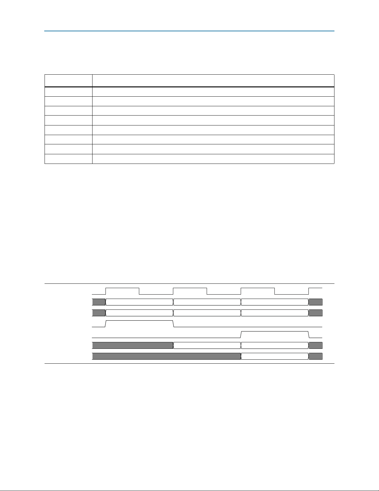
Chapter 5: IP Core Interfaces 5–9
clk
rx_st_data[63:32]
rx_st_data[31:0]
rx_st_sop
rx_st_eop
rx_st_be[7:4]
rx_st_be[3:0]
Header1 Data0 Data2
Header0 Header2 Data1
F F
F
Avalon-ST Interface
Tab le 5– 3 shows the byte ordering for header and data packets for Figure 5–5 through
Figure 5–13.
Table 5–3. Mapping Avalon-ST Packets to PCI Express TLPs
Packet TLP
Header0 pcie_hdr_byte0, pcie_hdr _byte1, pcie_hdr _byte2, pcie_hdr _byte3
Header1 pcie_hdr _byte4, pcie_hdr _byte5, pcie_hdr byte6, pcie_hdr _byte7
Header2 pcie_hdr _byte8, pcie_hdr _byte9, pcie_hdr _byte10, pcie_hdr _byte11
Header3 pcie_hdr _byte12, pcie_hdr _byte13, header_byte14, pcie_hdr _byte15
Data0 pcie_data_byte3, pcie_data_byte2, pcie_data_byte1, pcie_data_byte0
Data1 pcie_data_byte7, pcie_data_byte6, pcie_data_byte5, pcie_data_byte4
Data2 pcie_data_byte11, pcie_data_byte10, pcie_data_byte9, pcie_data_byte8
Data<n> pcie_data_byte<n>, pcie_data_byte<n-1>, pcie_data_byte<n>-2, pcie_data_byte<n-3>
Figure 5–5 illustrates the mapping of Avalon-ST RX packets to PCI Express TLPs for a
three dword header with non-qword aligned addresses with a 64-bit bus. In this
example, the byte address is unaligned and ends with 0x4, causing the first data to
correspond to
rx_st_data[63:32]
.
f For more information about the Avalon-ST protocol, refer to the Avalon Interface
Specifications.
1 The Avalon-ST protocol, as defined in Avalon Interface Specifications, is big endian, but
the IP Compiler for PCI Express packs symbols into words in little endian format.
Consequently, you cannot use the standard data format adapters that use the AvalonST interface.
Figure 5–5. 64-Bit Avalon-ST rx_st_data<n> Cycle Definition for 3-DWord Header TLPs with Non-QWord Aligned Address
August 2014 Altera Corporation IP Compiler for PCI Express User Guide
Page 96

5–10 Chapter 5: IP Core Interfaces
clk
rx_st_data[63:32]
rx_st_data[31:0]
rx_st_sop
rx_st_eop
rx_st_be[7:4]
rx_st_be[3:0]
Header 1 Data1 Data3
Header 0 Header2 Data0 Data2
F 1
FE
clk
rx_st_data[63:32]
rx_st_data[31:0]
rx_st_sop
rx_st_eop
rx_st_be[7:4]
rx_st_be[3:0]
header1 header3 data1
header0 header2 data0
F
F
Avalon-ST Interface
Figure 5–6 illustrates the mapping of Avalon-ST RX packets to PCI Express TLPs for a
three dword header with qword aligned addresses. Note that the byte enables
indicate the first byte of data is not valid and the last dword of data has a single valid
byte.
Figure 5–6. 64-Bit Avalon-ST rx_st_data<n> Cycle Definition for 3-DWord Header TLPs with QWord Aligned Address
(Note 1)
Note to Figure 5–6:
(1)
rx_st_be[7:4]
corresponds to
rx_st_data[63:32]. rx_st_be[3:0]
corresponds to
rx_st_data[31:0]
Figure 5–7 shows the mapping of Avalon-ST RX packets to PCI Express TLPs for TLPs
for a four dword with qword aligned addresses with a 64-bit bus.
Figure 5–7. 64-Bit Avalon-ST rx_st_data<n> Cycle Definitions for 4-DWord Header TLPs with QWord Aligned Addresses
IP Compiler for PCI Express User Guide August 2014 Altera Corporation
Page 97
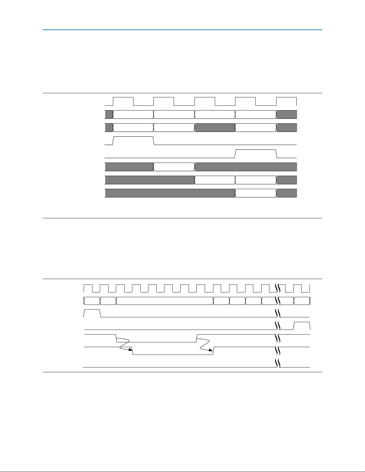
Chapter 5: IP Core Interfaces 5–11
clk
rx_st_data[63:32]
rx_st_data[31:0]
rx_st_sop
rx_st_eop
rx_st_bardec[7:0]
rx_st_be[7:4]
rx_st_be[3:0]
header1 header3 data0 data2
header0 header2 data1
10
C F
F
Avalon-ST Interface
Figure 5–8 shows the mapping of Avalon-ST RX packet to PCI Express TLPs for TLPs
for a four dword header with non-qword addresses with a 64-bit bus. Note that the
address of the first dword is 0x4. The address of the first enabled byte is 0x6. This
example shows one valid word in the first dword, as indicated by the
rx_st_be
signal.
Figure 5–8. 64-Bit Avalon-ST rx_st_data<n> Cycle Definitions for 4-DWord Header TLPs with Non-QWord Addresses
(Note 1)
Note to Figure 5–8:
(1)
rx_st_be[7:4]
corresponds to
rx_st_data[63:32]. rx_st_be[3:0]
Figure 5–9 illustrates the timing of the RX interface when the application
backpressures the IP Compiler for PCI Express by deasserting
rx_st_valid
In this example,
signal must deassert within three cycles after
rx_st_valid
the application is able to accept it.
Figure 5–9. 64-Bit Application Layer Backpressures Transaction Layer
clk
rx_st_data[63:0]
rx_st_sop
rx_st_eop
rx_st_ready
rx_st_valid
rx_st_err
000.010
CCCC0002CCCC0001 CC.CC.CC.CC.CC.CC
.
corresponds to
rx_st_data[31:0]
rx_st_ready
is deasserted in the next cycle.
.
rx_st_ready
rx_st_data
. The
is deasserted.
is held until
.
August 2014 Altera Corporation IP Compiler for PCI Express User Guide
Page 98

5–12 Chapter 5: IP Core Interfaces
Avalon-ST Interface
Figure 5–10 shows the mapping of 128-bit Avalon-ST RX packets to PCI Express TLPs
for TLPs with a three dword header and qword aligned addresses.
Figure 5–10. 128-Bit Avalon-ST rx_st_data<n> Cycle Definition for 3-DWord Header TLPs with QWord Aligned Addresses
clk
rx_st_valid
rx_st_data[127:96]
rx_st_data[95:64]
rx_st_data[63:32]
rx_st_data[31:0]
rx_st_bardec[7:0]
rx_st_sop
rx_st_eop
rx_st_empty
header2 data2
header1 data1 data<n>
header0 data0 data<n-1>
01
data3
Figure 5–11 shows the mapping of 128-bit Avalon-ST RX packets to PCI Express TLPs
for TLPs with a 3 dword header and non-qword aligned addresses.
Figure 5–11. 128-Bit Avalon-ST rx_st_data<n> Cycle Definition for 3-DWord Header TLPs with non-QWord Aligned
Addresses
clk
rx_st_valid
rx_st_data[127:96]
rx_st_data[95:64]
rx_st_data[63:32]
rx_st_data[31:0]
rx_st_sop
rx_st_eop
rx_st_empty
Data0
Header 2
Header 1 Data 2 Data (n)
Header 0 Data 1 Data (n-1)
Data 4
Data 3
IP Compiler for PCI Express User Guide August 2014 Altera Corporation
Page 99

Chapter 5: IP Core Interfaces 5–13
Avalon-ST Interface
Figure 5–12 shows the mapping of 128-bit Avalon-ST RX packets to PCI Express TLPs
for a four dword header with non-qword aligned addresses. In this example,
rx_st_empty
is low because the data ends in the upper 64 bits of
rx_st_data
.
Figure 5–12. 128-Bit Avalon-ST rx_st_data Cycle Definition for 4-DWord Header TLPs with non-QWord Aligned Addresses
clk
rx_st_valid
rx_st_data[127:96]
rx_st_data[95:64]
rx_st_data[63:32]
rx_st_data[31:0]
rx_st_sop
rx_st_eop
rx_st_empty
Header 3 Data 2
Header 2 Data 1
Header 1 Data 0
Header 0
Data n
Data n-1
Data n-2
Figure 5–13 shows the mapping of 128-bit Avalon-ST RX packets to PCI Express TLPs
for a four dword header with qword aligned addresses.
Figure 5–13. 128-Bit Avalon-ST rx_st_data Cycle Definition for 4-DWord Header TLPs with QWord Aligned Addresses
clk
rx_st_valid
rx_st_data[127:96]
rx_st_data[95:64]
rx_st_data[63:32]
rx_st_data[31:0]
rx_st_sop
rx_st_eop
rx_st_empty
Header3 Data3 Data n
Header 2 Data 2 Data n-1
Header 1 Data 1 Data n-2
Header 0 Data 0 Data n-3
f For a complete description of the TLP packet header formats, refer to Appendix A,
Transaction Layer Packet (TLP) Header Formats.
August 2014 Altera Corporation IP Compiler for PCI Express User Guide
Page 100

5–14 Chapter 5: IP Core Interfaces
clk
rx_st_data[127:0]
rx_st_sop
rx_st_eop
rx_st_empty
rx_st_ready
rx_st_valid
rx_st_err
0000
.
clk
rx_st_ready
rx_st_valid
rx_st_data[63:0]
rx_st_sop
rx_st_eop
h1 h2
data0 data1 data2 data3 data4 data5 data6
3 cycles
max latency
12345678 91110
Avalon-ST Interface
Figure 5–14 illustrates the timing of the RX interface when the application
backpressures the IP Compiler for PCI Express by deasserting
rx_st_valid
In this example,
signal must deassert within three cycles after
rx_st_valid
is deasserted in the next cycle.
rx_st_ready
rx_st_ready
rx_st_data
. The
is deasserted.
is held until
the application is able to accept it.
Figure 5–14. 128-Bit Application Layer Backpressures Hard IP Transaction Layer
Figure 5–15 illustrates the timing of the Avalon-ST RX interface. On this interface, the
core deasserts
application.
Figure 5–15. Avalon-ST RX Interface Timing
rx_st_valid
in response to the deassertion of
rx_st_ready
from the
IP Compiler for PCI Express User Guide August 2014 Altera Corporation
 Loading...