

Page 1

Integer Arithmetic IP Cores User Guide
Subscribe
Send Feedback
UG-01063
2014.12.19
101 Innovation Drive
San Jose, CA 95134
www.altera.com
Page 2

TOC-2
Integer Arithmetic IP Cores User Guide
Contents
Integer Arithmetic Megafunctions..................................................................... 1-1
LPM_COUNTER (Counter)................................................................................2-1
Design Example Files...................................................................................................................................1-2
Installing and Licensing IP Cores..............................................................................................................1-2
Customizing and Generating IP Cores.....................................................................................................1-2
IP Catalog and Parameter Editor...............................................................................................................1-3
Using the Parameter Editor........................................................................................................................1-4
Specifying IP Core Parameters and Options............................................................................................1-4
Specifying IP Core Parameters and Options (Legacy Parameter Editors)...........................................1-6
Files Generated for Altera IP Cores (Legacy Parameter Editor)............................................... 1-7
Upgrading IP Cores.....................................................................................................................................1-8
Migrating IP Cores to a Different Device...............................................................................................1-11
Simulating Altera IP Cores in other EDA Tools................................................................................... 1-12
Features......................................................................................................................................................... 2-1
Resource Utilization and Performance.....................................................................................................2-2
Verilog HDL Prototype...............................................................................................................................2-2
VHDL Component Declaration................................................................................................................ 2-3
VHDL LIBRARY_USE Declaration..........................................................................................................2-3
Ports...............................................................................................................................................................2-3
Parameters.....................................................................................................................................................2-5
LPM_DIVIDE (Divider)......................................................................................3-1
Features......................................................................................................................................................... 3-1
Resource Utilization and Performance.....................................................................................................3-1
Verilog HDL Prototype...............................................................................................................................3-2
VHDL Component Declaration................................................................................................................ 3-2
VHDL LIBRARY_USE Declaration..........................................................................................................3-3
Ports...............................................................................................................................................................3-3
Parameters.....................................................................................................................................................3-3
LPM_MULT (Multiplier)....................................................................................4-1
Features......................................................................................................................................................... 4-1
Resource Utilization and Performance.....................................................................................................4-1
Verilog HDL Prototype...............................................................................................................................4-2
VHDL Component Declaration................................................................................................................ 4-3
VHDL LIBRARY_USE Declaration..........................................................................................................4-3
LPM_MULT Ports.......................................................................................................................................4-3
LPM_MULT Parameters............................................................................................................................ 4-4
Altera Corporation
Page 3

Integer Arithmetic IP Cores User Guide
TOC-3
ALTECC (Error Correction Code: Encoder/Decoder).......................................5-1
ALTECC_ENCODER Features..................................................................................................................5-2
Resource Utilization and Performance.....................................................................................................5-3
Verilog HDL Prototype (ALTECC_ENCODER)....................................................................................5-5
Verilog HDL Prototype (ALTECC_DECODER)....................................................................................5-5
VHDL Component Declaration (ALTECC_ENCODER)..................................................................... 5-6
VHDL Component Declaration (ALTECC_DECODER)..................................................................... 5-6
VHDL LIBRARY_USE Declaration..........................................................................................................5-7
Ports (ALTECC_ENCODER)....................................................................................................................5-7
Ports (ALTECC_DECODER)....................................................................................................................5-7
Parameters (ALTECC_ENCODER)..........................................................................................................5-8
Parameters (ALTECC_DECODER)..........................................................................................................5-8
Design Example 1: ALTECC_ENCODER................................................................................................5-9
Understanding the Simulation Results......................................................................................... 5-9
Design Example 2: ALTECC_DECODER..............................................................................................5-12
Understanding the Simulation Results.......................................................................................5-12
ALTERA_MULT_ADD (Multiply-Adder)......................................................... 6-1
Features......................................................................................................................................................... 6-2
Pre-adder...........................................................................................................................................6-3
Systolic Delay Register.....................................................................................................................6-6
Pre-load Constant............................................................................................................................6-9
Double Accumulator.......................................................................................................................6-9
Verilog HDL Prototype.............................................................................................................................6-10
VHDL Component Declaration.............................................................................................................. 6-10
VHDL LIBRARY_USE Declaration........................................................................................................6-10
Ports.............................................................................................................................................................6-10
ALTERA_MULT_ADD Parameters.......................................................................................................6-12
Design Example: Implementing a Simple Finite Impulse Response (FIR) Filter.............................6-19
Understanding the Simulation Results...................................................................................................6-20
ALTMEMMULT (Memory-based Constant Coefficient Multiplier).................7-1
Features......................................................................................................................................................... 7-1
Resource Utilization and Performance.....................................................................................................7-2
Verilog HDL Prototype...............................................................................................................................7-2
VHDL Component Declaration................................................................................................................ 7-3
Ports...............................................................................................................................................................7-3
Parameters.....................................................................................................................................................7-4
Design Example: 8 × 8 Multiplier..............................................................................................................7-5
Understanding the Simulation Results..................................................................................................... 7-6
ALTMULT_ACCUM (Multiply-Accumulate)....................................................8-1
Features......................................................................................................................................................... 8-2
Resource Utilization and Performance.....................................................................................................8-2
Altera Corporation
Page 4

TOC-4
Integer Arithmetic IP Cores User Guide
Verilog HDL Prototype...............................................................................................................................8-4
VHDL Component Declaration................................................................................................................ 8-4
VHDL LIBRARY_USE Declaration..........................................................................................................8-4
ALTMULT_ACCUM Ports........................................................................................................................8-4
ALTMULT_ACCUM Parameters.............................................................................................................8-6
Design Example: Shift Accumulator.......................................................................................................8-19
Understanding the Simulation Results...................................................................................................8-19
ALTMULT_ADD (Multiply-Adder)...................................................................9-1
Features......................................................................................................................................................... 9-3
Pre-adder...........................................................................................................................................9-4
Systolic Delay Register.....................................................................................................................9-7
Pre-load Constant..........................................................................................................................9-10
Double Accumulator.....................................................................................................................9-10
Resource Utilization and Performance...................................................................................................9-11
Verilog HDL Prototype.............................................................................................................................9-11
VHDL Component Declaration.............................................................................................................. 9-11
VHDL LIBRARY_USE Declaration........................................................................................................9-12
ALTMULT_ADD Ports............................................................................................................................9-12
ALTMULT_ADD Parameters................................................................................................................. 9-14
Design Example: Implementing a Simple Finite Impulse Response (FIR) Filter.............................9-34
Understanding the Simulation Results...................................................................................................9-35
ALTMULT_COMPLEX (Complex Multiplier)................................................ 10-1
Complex Multiplication............................................................................................................................10-2
Canonical Representation.........................................................................................................................10-2
Conventional Representation...................................................................................................................10-3
Features....................................................................................................................................................... 10-3
Resource Utilization and Performance...................................................................................................10-4
Verilog HDL Prototype.............................................................................................................................10-4
VHDL Component Declaration.............................................................................................................. 10-5
VHDL LIBRARY_USE Declaration........................................................................................................10-5
ALTMULT_COMPLEX Ports.................................................................................................................10-6
ALTMULT_COMPLEX Parameters.......................................................................................................10-6
Design Example: Multiplication of 8-bit Complex Numbers Using Canonical Representation...
10-8
Understanding the Simulation Results...................................................................................................10-8
ALTSQRT (Integer Square Root)..................................................................... 11-1
Features....................................................................................................................................................... 11-1
Resource Utilization and Performance...................................................................................................11-1
Verilog HDL Prototype.............................................................................................................................11-2
VHDL Component Declaration.............................................................................................................. 11-2
VHDL LIBRARY_USE Declaration........................................................................................................11-3
Ports.............................................................................................................................................................11-3
Parameters.................................................................................................................................................. 11-3
Altera Corporation
Page 5

Integer Arithmetic IP Cores User Guide
Design Example: 9-bit Square Root.........................................................................................................11-4
Understanding the Simulation Results...................................................................................................11-4
TOC-5
PARALLEL_ADD (Parallel Adder).................................................................. 12-1
Feature.........................................................................................................................................................12-1
Resource Utilization and Performance...................................................................................................12-1
Verilog HDL Prototype.............................................................................................................................12-2
VHDL Component Declaration.............................................................................................................. 12-2
VHDL LIBRARY_USE Declaration........................................................................................................12-3
Ports.............................................................................................................................................................12-3
Parameters.................................................................................................................................................. 12-4
Design Example: Shift Accumulator.......................................................................................................12-4
Understanding the Simulation Results...................................................................................................12-5
Document Revision History..............................................................................13-1
Altera Corporation
Page 6

2014.12.19
www.altera.com
101 Innovation Drive, San Jose, CA 95134
Integer Arithmetic Megafunctions
1
UG-01063
Subscribe
Send Feedback
You can use Altera® integer megafunction IP cores to perform mathematical operations in your design.
These functions offer more efficient logic synthesis and device implementation than coding your own
functions. You can customize the IP cores to accommodate your design requirements.
Altera integer arithmetic megafunctions are divided into the following two categories:
• Library of parameterized modules (LPM) IP cores
• Altera-specific (ALT) IP cores
The following table lists the integer arithmetic IP cores.
Table 1-1: List of IP Cores
IP Cores Function Overview
LPM Megafunctions
LPM_COUNTER (Counter) Counter
LPM_DIVIDE (Divider) Divider
LPM_MULT (Multiplier) Multiplier
Altera-specific (ALT) Megafunctions
ALTECC ECC Encoder/Decoder
ALTERA_MULT_ADD (Multiply-Adder) Multiplier-Adder
ALTMEMMULT (Memory-based Constant
Memory-based Constant Coefficient Multiplier
Coefficient Multiplier)
ALTMULT_ACCUM (Multiply-Accumulate) Multiplier-Accumulator
ALTERA_MULT_ADD (Multiply-Adder) Multiplier-Adder
ALTMULT_COMPLEX (Complex Multiplier) Complex Multiplier
ALTSQRT (Integer Square Root) Integer Square-Root
PARALLEL_ADD (Parallel Adder) Parallel Adder
If you are unfamiliar with IP cores, refer to the Introduction to IP Cores User Guide.
©
2014 Altera Corporation. All rights reserved. ALTERA, ARRIA, CYCLONE, ENPIRION, MAX, MEGACORE, NIOS, QUARTUS and STRATIX words and logos are
trademarks of Altera Corporation and registered in the U.S. Patent and Trademark Office and in other countries. All other words and logos identified as
trademarks or service marks are the property of their respective holders as described at www.altera.com/common/legal.html. Altera warrants performance
of its semiconductor products to current specifications in accordance with Altera's standard warranty, but reserves the right to make changes to any
products and services at any time without notice. Altera assumes no responsibility or liability arising out of the application or use of any information,
product, or service described herein except as expressly agreed to in writing by Altera. Altera customers are advised to obtain the latest version of device
specifications before relying on any published information and before placing orders for products or services.
ISO
9001:2008
Registered
Page 7

acds
quartus - Contains the Quartus II software
ip - Contains the Altera IP Library and third-party IP cores
altera - Contains the Altera IP Library source code
<IP core name> - Contains the IP core source files
1-2
Design Example Files
Altera also provides floating-point IP cores. For more information about the floating-point IP cores, refer
to the Floating-Point IP Cores User Guide.
Design Example Files
Altera provides design example files that are simulated in the ModelSim®-Altera software to generate a
waveform display of the device behavior.
You should be familiar with the ModelSim-Altera software before using the design examples. To get
started with the ModelSim-Altera software, refer to the ModelSim-Altera Software Support page on the
Altera website. The support page includes links to such topics as installation, usage, and troubleshooting.
For more details about the design example for a specific IP core, refer to the “Design Example” section for
that megafunction.
Design examples are provided only for some IP cores in this user guide.
Installing and Licensing IP Cores
The Altera IP Library provides many useful IP core functions for production use without purchasing an
additional license. You can evaluate any Altera® IP core in simulation and compilation in the Quartus® II
software using the OpenCore® evaluation feature. Some Altera IP cores, such as MegaCore® functions,
require that you purchase a separate license for production use. You can use the OpenCore Plus feature to
evaluate IP that requires purchase of an additional license until you are satisfied with the functionality and
performance. After you purchase a license, visit the Self Service Licensing Center to obtain a license
number for any Altera product.
UG-01063
2014.12.19
Figure 1-1: IP Core Installation Path
Note:
The default IP installation directory on Windows is <drive>:\altera\<version number>; on Linux it is
<home directory>/altera/ <version number>.
Related Information
• Altera Licensing Site
• Altera Software Installation and Licensing Manual
Customizing and Generating IP Cores
You can customize IP cores to support a wide variety of applications. The Quartus II IP Catalog and
parameter editor allow you to quickly select and configure IP core ports, features, and output files.
Altera Corporation
Integer Arithmetic Megafunctions
Send Feedback
Page 8
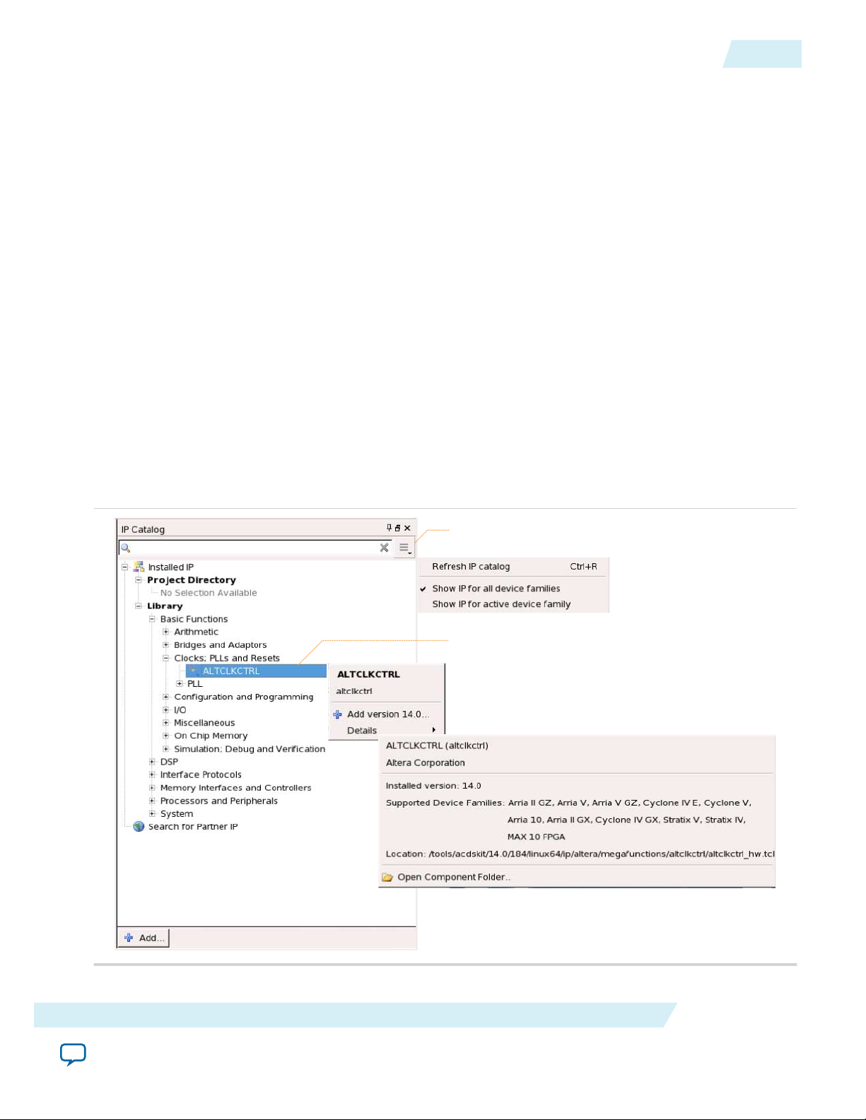
Search and filter IP for your target device
Double-click to customize, right-click for information
UG-01063
2014.12.19
IP Catalog and Parameter Editor
The Quartus II IP Catalog (Tools > IP Catalog) and parameter editor help you easily customize and
integrate IP cores into your project. You can use the IP Catalog and parameter editor to select, customize,
and generate files representing your custom IP variation.
Note: The IP Catalog (Tools > IP Catalog) and parameter editor replace the MegaWizard™ Plug-In
Manager for IP selection and parameterization, beginning in Quartus II software version 14.0. Use
the IP Catalog and parameter editor to locate and paramaterize Altera IP cores.
The IP Catalog lists IP cores available for your design. Double-click any IP core to launch the parameter
editor and generate files representing your IP variation. The parameter editor prompts you to specify an
IP variation name, optional ports, and output file generation options. The parameter editor generates a
top-level Qsys system file (.qsys) or Quartus II IP file (.qip) representing the IP core in your project. You
can also parameterize an IP variation without an open project.
Use the following features to help you quickly locate and select an IP core:
• Filter IP Catalog to Show IP for active device family or Show IP for all device families.
• Search to locate any full or partial IP core name in IP Catalog. Click Search for Partner IP, to access
partner IP information on the Altera website.
• Right-click an IP core name in IP Catalog to display details about supported devices, open the IP core's
installation folder, andor view links to documentation.
IP Catalog and Parameter Editor
1-3
Figure 1-2: Quartus II IP Catalog
Integer Arithmetic Megafunctions
Send Feedback
Altera Corporation
Page 9
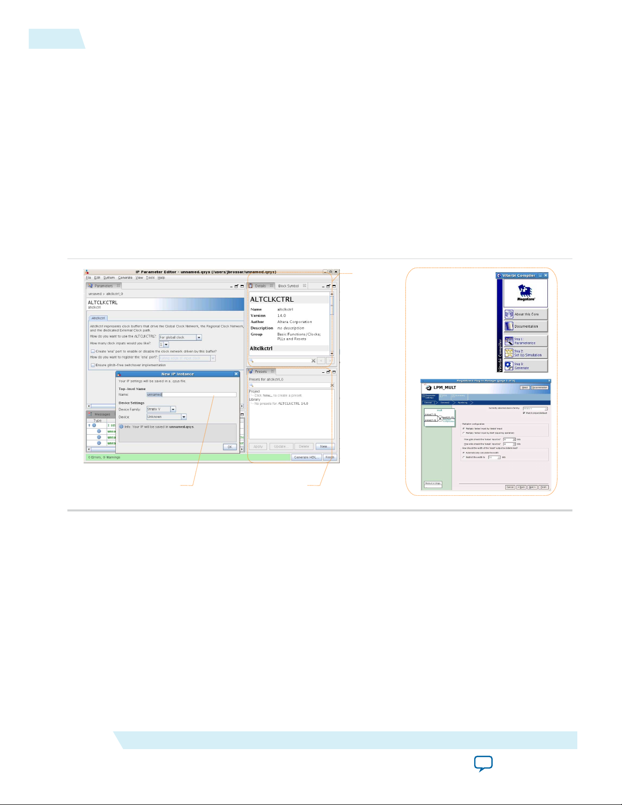
View IP port
and parameter
details
Apply preset parameters for
specific applications
Specify your IP variation name
and target device
Legacy parameter
editors
1-4
Using the Parameter Editor
Note: The IP Catalog is also available in Qsys (View > IP Catalog). The Qsys IP Catalog includes
exclusive system interconnect, video and image processing, and other system-level IP that are not
available in the Quartus II IP Catalog. For more information about using the Qsys IP Catalog, refer
to Creating a System with Qsys in the Quartus II Handbook.
Using the Parameter Editor
The parameter editor helps you to configure IP core ports, parameters, and output file generation options.
• Use preset settings in the parameter editor (where provided) to instantly apply preset parameter values
for specific applications.
• View port and parameter descriptions, and links to documentation.
• Generate testbench systems or example designs (where provided).
Figure 1-3: IP Parameter Editors
UG-01063
2014.12.19
Specifying IP Core Parameters and Options
Altera Corporation
The parameter editor GUI allows you to quickly configure your custom IP variation. Use the following
steps to specify IP core options and parameters in the Quartus II software. Refer to Specifying IP Core
Parameters and Options (Legacy Parameter Editors) for configuration of IP cores using the legacy
parameter editor.
Integer Arithmetic Megafunctions
Send Feedback
Page 10

UG-01063
2014.12.19
Specifying IP Core Parameters and Options
1-5
1. In the IP Catalog (Tools > IP Catalog), locate and double-click the name of the IP core to customize.
The parameter editor appears.
2. Specify a top-level name for your custom IP variation. The parameter editor saves the IP variation
settings in a file named <your_ip>.qsys. Click OK.
3. Specify the parameters and options for your IP variation in the parameter editor, including one or
more of the following. Refer to your IP core user guide for information about specific IP core
parameters.
• Optionally select preset parameter values if provided for your IP core. Presets specify initial
parameter values for specific applications.
• Specify parameters defining the IP core functionality, port configurations, and device-specific
features.
• Specify options for processing the IP core files in other EDA tools.
4. Click Generate HDL, the Generation dialog box appears.
5. Specify output file generation options, and then click Generate. The IP variation files generate
according to your specifications.
6. To generate a simulation testbench, click Generate > Generate Testbench System.
7. To generate an HDL instantiation template that you can copy and paste into your text editor, click
Generate > HDL Example.
8. Click Finish. The parameter editor adds the top-level .qsys file to the current project automatically. If
you are prompted to manually add the .qsys file to the project, click Project > Add/Remove Files in
Project to add the file.
9. After generating and instantiating your IP variation, make appropriate pin assignments to connect
ports.
Integer Arithmetic Megafunctions
Send Feedback
Altera Corporation
Page 11
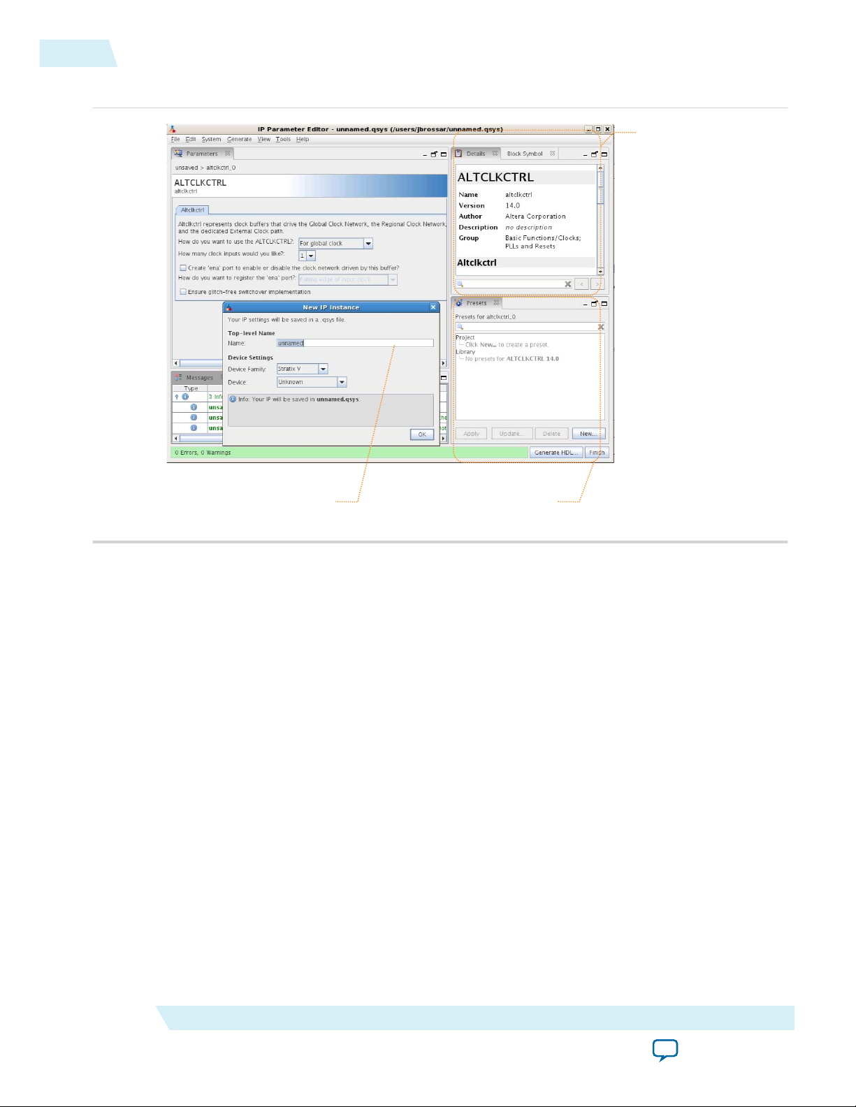
View IP port
and parameter
details
Apply preset parameters for
specific applications
Specify your IP variation name
and target device
1-6
Specifying IP Core Parameters and Options (Legacy Parameter Editors)
Figure 1-4: IP Parameter Editor
UG-01063
2014.12.19
Specifying IP Core Parameters and Options (Legacy Parameter Editors)
Some IP cores use a legacy version of the parameter editor for configuration and generation. Use the
following steps to configure and generate an IP variation using a legacy parameter editor.
Note:
The legacy parameter editor generates a different output file structure than the latest parameter
editor. Refer to Specifying IP Core Parameters and Options for configuration of IP cores that use the
latest parameter editor.
Altera Corporation
Integer Arithmetic Megafunctions
Send Feedback
Page 12
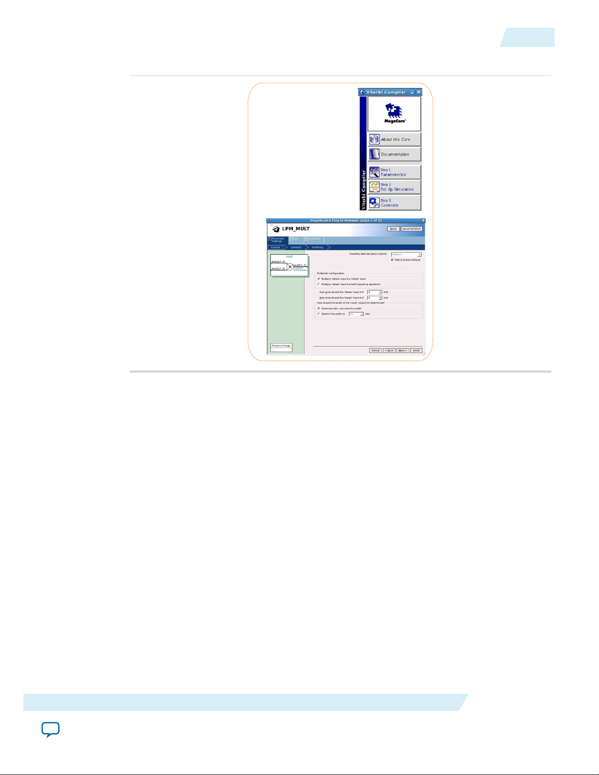
Legacy parameter
editors
UG-01063
2014.12.19
Files Generated for Altera IP Cores (Legacy Parameter Editor)
Figure 1-5: Legacy Parameter Editors
1-7
1. In the IP Catalog (Tools > IP Catalog), locate and double-click the name of the IP core to customize.
The parameter editor appears.
2. Specify a top-level name and output HDL file type for your IP variation. This name identifies the IP
core variation files in your project. Click OK.
3. Specify the parameters and options for your IP variation in the parameter editor. Refer to your IP core
user guide for information about specific IP core parameters.
4. Click Finish or Generate (depending on the parameter editor version). The parameter editor generates
the files for your IP variation according to your specifications. Click Exit if prompted when generation
is complete. The parameter editor adds the top-level .qip file to the current project automatically.
Note:
To manually add an IP variation generated with legacy parameter editor to a project, click
Project > Add/Remove Files in Project and add the IP variation .qip file.
Files Generated for Altera IP Cores (Legacy Parameter Editor)
The Quartus II software version generates the following output for your IP core that uses the legacy
parameter editor.
Integer Arithmetic Megafunctions
Send Feedback
Altera Corporation
Page 13
Notes:
1. If supported and enabled for your IP variation
2. If functional simulation models are generated
<Project Directory>
<your_ip>_bb.v - Verilog HDL black box EDA synthesis file
<your_ip>_inst.v or .vhd - Sample instantiation template
synthesis - IP synthesis files
<your_ip>.qip - Lists files for synthesis
testbench - Simulation testbench files
1
<testbench_hdl_files>
<simulator_vendor> - Testbench for supported simulators
<simulation_testbench_files>
<your_ip>.v or .vhd - Top-level IP variation synthesis file
simulation - IP simulation files
<your_ip>.sip - NativeLink simulation integration file
<simulator vendor> - Simulator setup scripts
<simulator_setup_scripts>
<your_ip> - IP core variation files
<your_ip>.qip or .qsys - System or IP integration file
<your_ip>_generation.rpt - IP generation report
<your_ip>.bsf - Block symbol schematic file
<your_ip>.ppf - XML I/O pin information file
<your_ip>.spd - Combines individual simulation startup scripts
1
<your_ip>.html - Contains memory map
<your_ip>.sopcinfo - Software tool-chain integration file
<your_ip>_syn.v or .vhd - Timing & resource estimation netlist
1
<your_ip>.debuginfo - Lists files for synthesis
<your_ip>.v, .vhd, .vo, .vho - HDL or IPFS models
2
<your_ip>_tb - Testbench for supported simulators
<your_ip>_tb.v or .vhd - Top-level HDL testbench file
1-8
Upgrading IP Cores
Figure 1-6: IP Core Generated Files
UG-01063
2014.12.19
Upgrading IP Cores
IP core variants generated with a previous version of the Quartus II software may require upgrading
before use in the current version of the Quartus II software. Click Project > Upgrade IP Components to
identify and upgrade IP core variants.
The Upgrade IP Components dialog box provides instructions when IP upgrade is required, optional, or
unsupported for specific IP cores in your design. You must upgrade IP cores that require it before you can
Altera Corporation
Integer Arithmetic Megafunctions
Send Feedback
Page 14

UG-01063
2014.12.19
compile the IP variation in the current version of the Quartus II software. Many Altera IP cores support
automatic upgrade.
The upgrade process renames and preserves the existing variation file (.v, .sv, or .vhd) as <my_variant>_
BAK.v, .sv, .vhd in the project directory.
Table 1-2: IP Core Upgrade Status
IP Core Status Corrective Action
Upgrading IP Cores
1-9
Required Upgrade IP
Components
Optional Upgrade IP
Components
You must upgrade the IP variation before compiling in the current version of
the Quartus II software.
Upgrade is optional for this IP variation in the current version of the Quartus
II software. You can upgrade this IP variation to take advantage of the latest
development of this IP core. Alternatively you can retain previous IP core
characteristics by declining to upgrade.
Upgrade Unsupported Upgrade of the IP variation is not supported in the current version of the
Quartus II software due to IP core end of life or incompatibility with the
current version of the Quartus II software. You are prompted to replace the
obsolete IP core with a current equivalent IP core from the IP Catalog.
Before you begin
• Archive the Quartus II project containing outdated IP cores in the original version of the Quartus II
software: Click Project > Archive Project to save the project in your previous version of the Quartus II
software. This archive preserves your original design source and project files.
• Restore the archived project in the latest version of the Quartus II software: Click Project > Restore
Archived Project. Click OK if prompted to change to a supported device or overwrite the project
database. File paths in the archive must be relative to the project directory. File paths in the archive
must reference the IP variation .v or .vhd file or .qsys file (not the .qip file).
1. In the latest version of the Quartus II software, open the Quartus II project containing an outdated IP
core variation. The Upgrade IP Components dialog automatically displays the status of IP cores in
your project, along with instructions for upgrading each core. Click Project > Upgrade IP
Components to access this dialog box manually.
2. To simultaneously upgrade all IP cores that support automatic upgrade, click Perform Automatic
Upgrade. The Status and Version columns update when upgrade is complete. Example designs
provided with any Altera IP core regenerate automatically whenever you upgrade the IP core.
Integer Arithmetic Megafunctions
Send Feedback
Altera Corporation
Page 15
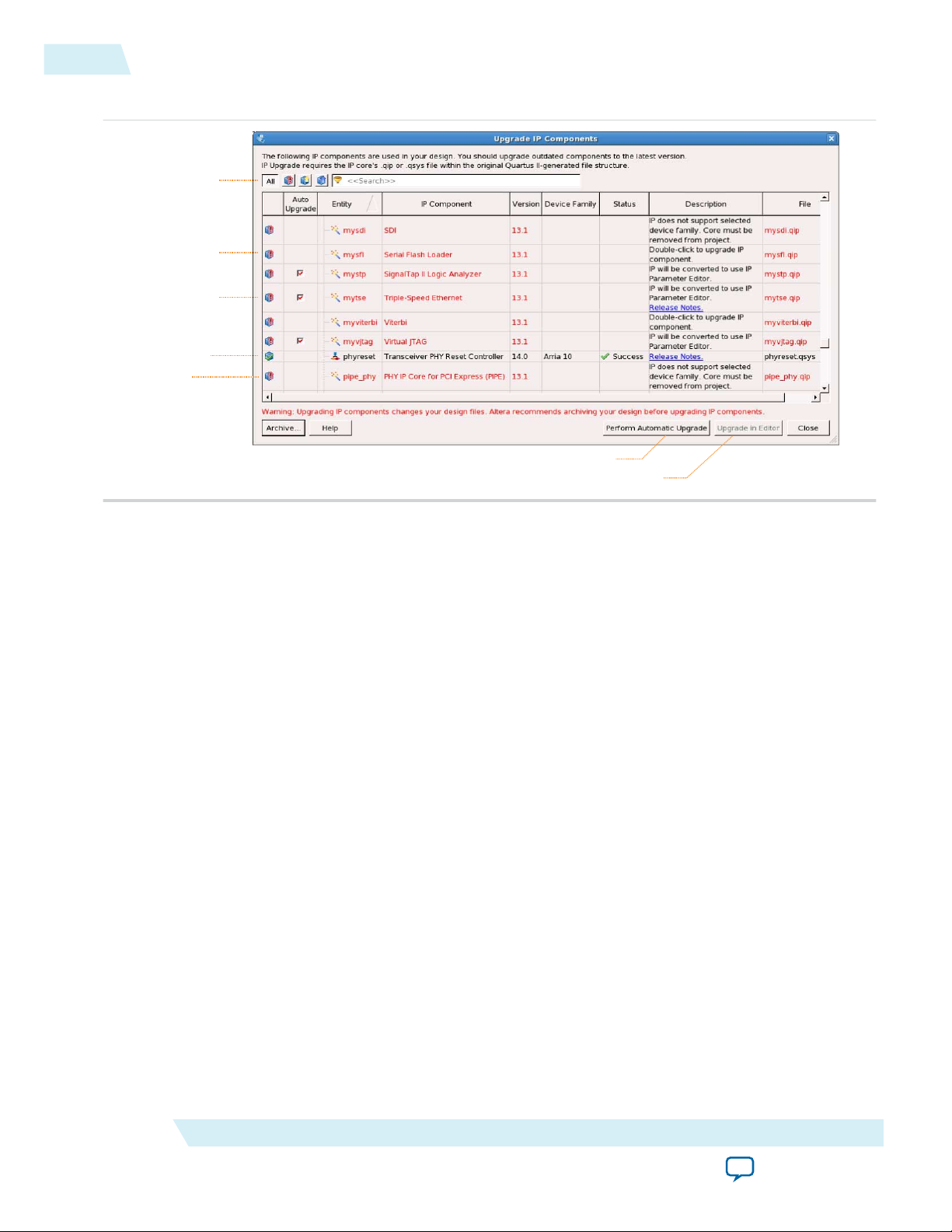
Displays upgrade
status for all IP cores
in the Project
Upgrades all IP core that support “Auto Upgrade”
Upgrades individual IP cores unsupported by “Auto Upgrade”
Checked IP cores
support “Auto Upgrade”
Successful
“Auto Upgrade”
Upgrade
unavailable
Double-click to
individually migrate
1-10
Upgrading IP Cores
Figure 1-7: Upgrading IP Cores
UG-01063
2014.12.19
Example 1-1: Upgrading IP Cores at the Command Line
You can upgrade IP cores that support auto upgrade at the command line. IP cores that do not
support automatic upgrade do not support command line upgrade.
• To upgrade a single IP core that supports auto-upgrade, type the following command:
quartus_sh –ip_upgrade –variation_files <my_ip_filepath/my_ip>.<hdl>
<qii_project>
Example:
quartus_sh -ip_upgrade -variation_files mega/pll25.v hps_testx
• To simultaneously upgrade multiple IP cores that support auto-upgrade, type the following
command:
quartus_sh –ip_upgrade –variation_files “<my_ip_filepath/my_ip1>.<hdl>;
<my_ip_filepath/my_ip2>.<hdl>” <qii_project>
Example:
quartus_sh -ip_upgrade -variation_files "mega/pll_tx2.v;mega/pll3.v"
hps_testx
IP cores older than Quartus II software version 12.0 do not support upgrade.
Note:
Altera verifies that the current version of the Quartus II software compiles the
previous version of each IP core. The Altera IP Release Notes reports any verifica‐
tion exceptions for Altera IP cores. Altera does not verify compilation for IP cores
older than the previous two releases.
Altera Corporation
Integer Arithmetic Megafunctions
Send Feedback
Page 16

UG-01063
2014.12.19
Related Information
Altera IP Release Notes
Migrating IP Cores to a Different Device
IP migration allows you to target the latest device families with IP originally generated for a different
device. Some Altera IP cores require individual migration to upgrade. The Upgrade IP Components
dialog box prompts you to double-click IP cores that require individual migration.
1. To display IP cores requiring migration, click Project > Upgrade IP Components. The Description
field prompts you to double-click IP cores that require individual migration.
2. Double-click the IP core name, and then click OK after reading the information panel.
The parameter editor appears showing the original IP core parameters.
3. For the Currently selected device family, turn off Match project/default, and then select the new
target device family.
4. Click Finish, and then click Finish again to migrate the IP variation using best-effort mapping to new
parameters and settings. Click OK if you are prompted that the IP core is unsupported for the current
device. A new parameter editor opens displaying best-effort mapped parameters.
5. Click Generate HDL, and then confirm the Synthesis and Simulation file options. Verilog is the
parameter editor default HDL for synthesis files. If your original IP core was generated for VHDL,
select VHDL to retain the original output HDL format.
6. To regenerate the new IP variation for the new target device, click Generate. When generation is
complete, click Close.
7. Click Finish to complete migration of the IP core. Click OK if you are prompted to overwrite IP core
files. The Device Family column displays the migrated device support. The migration process replaces
<my_ip>.qip with the <my_ip>.qsys top-level IP file in your project.
Migrating IP Cores to a Different Device
1-11
If migration does not replace <my_ip>.qip with <my_ip>.qsys, click Project > Add/Remove
Note:
Files in Project to replace the file in your project.
8. Review the latest parameters in the parameter editor or generated HDL for correctness. IP migration
may change ports, parameters, or functionality of the IP core. During migration, the IP core's HDL
generates into a library that is different from the original output location of the IP core. Update any
assignments that reference outdated locations. If your upgraded IP core is represented by a symbol in a
supporting Block Design File schematic, replace the symbol with the newly generated <my_ip>.bsf
after migration.
The migration process may change the IP variation interface, parameters, and functionality.
Note:
This may require you to change your design or to re-parameterize your variant after the
Upgrade IP Components dialog box indicates that migration is complete. The Description
field identifies IP cores that require design or parameter changes.
Related Information
Altera IP Release Notes
Integer Arithmetic Megafunctions
Send Feedback
Altera Corporation
Page 17
Post-fit timing
simulation netlist
Post-fit timing
simulation (3)
Post-fit functional
simulation netlist
Post-fit functional
simulation
Analysis & Synthesis
Fitter
(place-and-route)
TimeQuest Timing Analyzer
Device Programmer
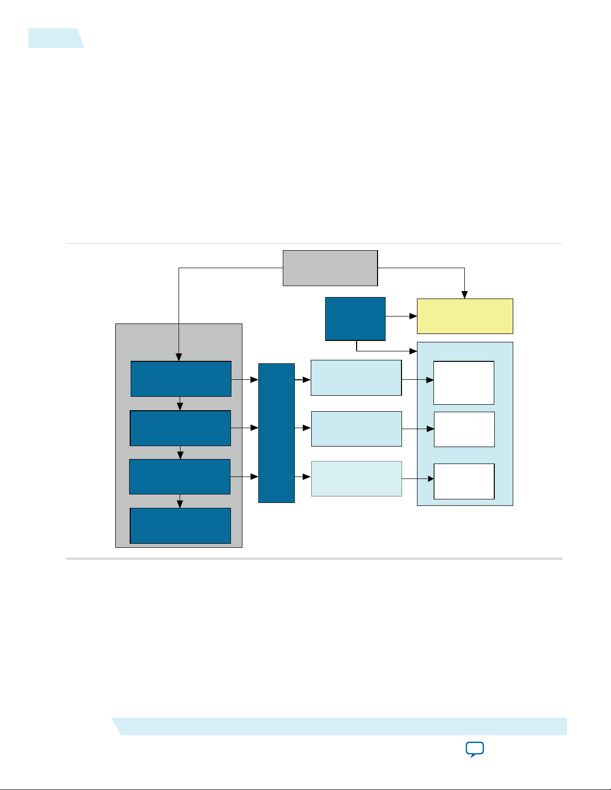
Quartus II
Design Flow
Gate-Level Simulation
Post-synthesis
functional
simulation
Post-synthesis functional
simulation netlist
(Optional) Post-fit
timing simulation
RTL Simulation
Design Entry
(HDL, Qsys, DSP Builder)
Altera Simulation
Models
EDA
Netlist
Writer
1-12
Simulating Altera IP Cores in other EDA Tools
Simulating Altera IP Cores in other EDA Tools
The Quartus II software supports RTL and gate-level design simulation of Altera IP cores in supported
EDA simulators. Simulation involves setting up your simulator working environment, compiling
simulation model libraries, and running your simulation.
You can use the functional simulation model and the testbench or example design generated with your IP
core for simulation. The functional simulation model and testbench files are generated in a project
subdirectory. This directory may also include scripts to compile and run the testbench. For a complete list
of models or libraries required to simulate your IP core, refer to the scripts generated with the testbench.
You can use the Quartus II NativeLink feature to automatically generate simulation files and scripts.
NativeLink launches your preferred simulator from within the Quartus II software.
Figure 1-8: Simulation in Quartus II Design Flow
UG-01063
2014.12.19
Altera Corporation
Note: Post-fit timing simulation is not supported for 28nm and later device archetectures. Altera IP
supports a variety of simulation models, including simulation-specific IP functional simulation
models and encrypted RTL models, and plain text RTL models. These are all cycle-accurate
models. The models support fast functional simulation of your IP core instance using industrystandard VHDL or Verilog HDL simulators. For some cores, only the plain text RTL model is
generated, and you can simulate that model. Use the simulation models only for simulation and
not for synthesis or any other purposes. Using these models for synthesis creates a nonfunctional
design.
Integer Arithmetic Megafunctions
Send Feedback
Page 18

UG-01063
2014.12.19
Related Information
Simulating Altera Designs
Simulating Altera IP Cores in other EDA Tools
1-13
Integer Arithmetic Megafunctions
Send Feedback
Altera Corporation
Page 19
2014.12.19
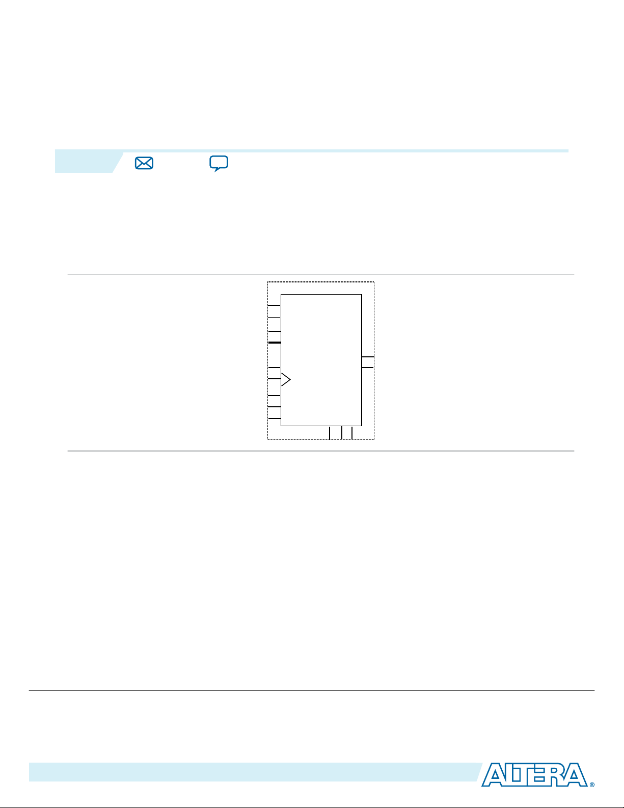
ssclr
sload
inst
LPM_COUNTER
q[]
sset
cout
data[]
clk_en
cnt_en
cin
aclr
aload
aset
updown
www.altera.com
101 Innovation Drive, San Jose, CA 95134
LPM_COUNTER (Counter)
2
UG-01063
Subscribe
Send Feedback
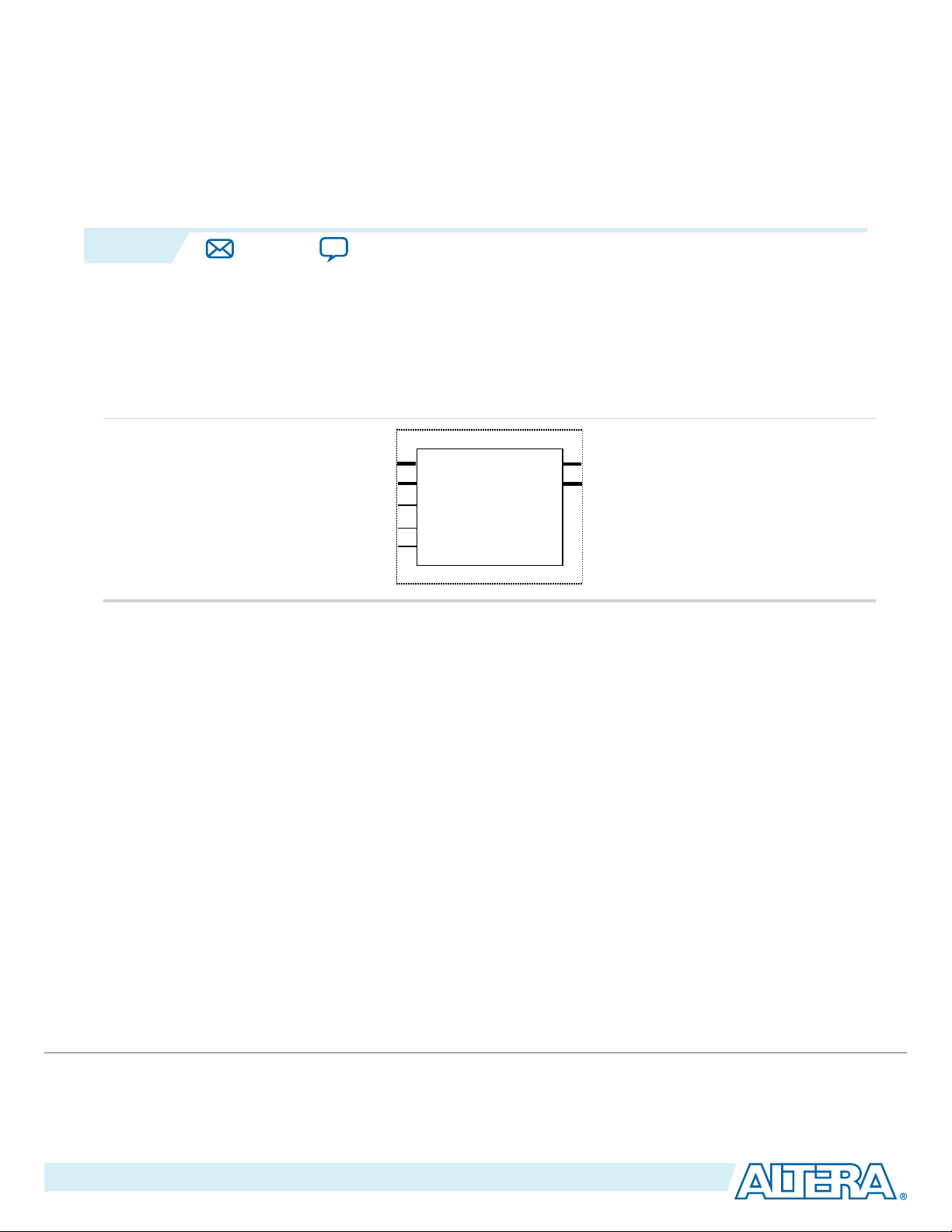
The LPM_COUNTER megafunction is a binary counter that creates up counters, down counters and up
or down counters with outputs of up to 256 bits wide.
The following figure shows the ports for the LPM_COUNTER megafunction.
Figure 2-1: LPM_COUNTER Ports
Features
The LPM_COUNTER megafunction offers the following features:
• Generates up, down, and up/down counters
• Generates the following counter types:
• Plain binary— the counter increments starting from zero or decrements starting from 255
• Modulus—the counter increments to or decrements from the modulus value specified by the user
• Supports optional synchronous clear, load, and set input ports
• Supports optional asynchronous clear, load, and set input ports
• Supports optional count enable and clock enable input ports
©
trademarks of Altera Corporation and registered in the U.S. Patent and Trademark Office and in other countries. All other words and logos identified as
trademarks or service marks are the property of their respective holders as described at www.altera.com/common/legal.html. Altera warrants performance
of its semiconductor products to current specifications in accordance with Altera's standard warranty, but reserves the right to make changes to any
products and services at any time without notice. Altera assumes no responsibility or liability arising out of the application or use of any information,
product, or service described herein except as expressly agreed to in writing by Altera. Altera customers are advised to obtain the latest version of device
specifications before relying on any published information and before placing orders for products or services.
• Supports optional carry-in and carry-out ports
2014 Altera Corporation. All rights reserved. ALTERA, ARRIA, CYCLONE, ENPIRION, MAX, MEGACORE, NIOS, QUARTUS and STRATIX words and logos are
and repeats
ISO
9001:2008
Registered
Page 20

2-2
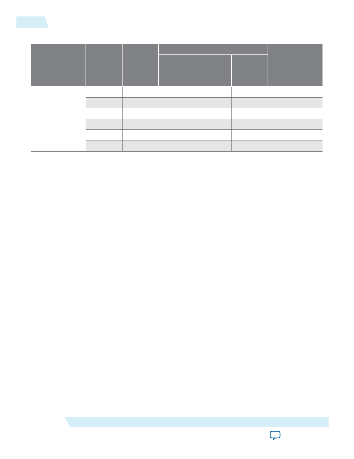
Resource Utilization and Performance
Resource Utilization and Performance
The following table provides resource utilization and performance information for the LPM_COUNTER
megafunction.
Table 2-1: LPM_COUNTER Resource Utilization and Performance
UG-01063
2014.12.19
Logic Usage
Device family
Stratix III
Stratix IV
Input data
width
Output
latency
Adaptive
Look-Up
Table (ALUT)
Dedicated
Logic
Register
(DLR)
Adaptive
Logic
Module
(ALM)
4 - 9 4 6 723
8 - 9 8 5 808
16 - 17 16 9 705
24 - 25 24 13 583
32 - 33 32 17 489
64 - 65 64 33 329
4 - 9 4 6 768
8 - 9 8 5 896
16 - 17 16 9 825
24 - 25 24 13 716
32 - 33 32 17 639
64 - 65 64 33 470
f
MAX
(MHz)
(1)
Verilog HDL Prototype
The following Verilog HDL prototype is located in the Verilog Design File (.v) lpm.v in the <Quartus II
installation directory>\eda\synthesis directory.
module lpm_counter ( q, data, clock, cin, cout, clk_en, cnt_en, updown,
aset, aclr, aload, sset, sclr, sload, eq );
parameter lpm_type = "lpm_counter";
parameter lpm_width = 1;
parameter lpm_modulus = 0;
parameter lpm_direction = "UNUSED";
parameter lpm_avalue = "UNUSED";
parameter lpm_svalue = "UNUSED";
parameter lpm_pvalue = "UNUSED";
parameter lpm_port_updown = "PORT_CONNECTIVITY";
parameter lpm_hint = "UNUSED";
output [lpm_width-1:0] q;
(1)
The performance of the megafunction is dependant on the value of the maximum allowable ceiling f
that the selected device can achieve. Therefore, results may vary from the numbers stated in this column.
Altera Corporation
MAX
LPM_COUNTER (Counter)
Send Feedback
Page 21

UG-01063
2014.12.19
output cout;
output [15:0] eq;
input cin;
input [lpm_width-1:0] data;
input clock, clk_en, cnt_en, updown;
input aset, aclr, aload;
input sset, sclr, sload;
endmodule
VHDL Component Declaration
The VHDL component declaration is located in the VHDL Design File (.vhd) LPM_PACK.vhd in the
<Quartus II installation directory>\libraries\vhdl\lpm directory.
component LPM_MULT
generic ( LPM_WIDTHA : natural;
LPM_WIDTHB : natural;
LPM_WIDTHS : natural := 1;
LPM_WIDTHP : natural;
LPM_REPRESENTATION : string := "UNSIGNED";
LPM_PIPELINE : natural := 0;
LPM_TYPE: string := L_MULT;
LPM_HINT : string := "UNUSED");
port ( DATAA : in std_logic_vector(LPM_WIDTHA-1 downto 0);
DATAB : in std_logic_vector(LPM_WIDTHB-1 downto 0);
ACLR : in std_logic := '0';
CLOCK : in std_logic := '0';
CLKEN : in std_logic := '1';
SUM : in std_logic_vector(LPM_WIDTHS-1 downto 0) := (OTHERS => '0');
RESULT : out std_logic_vector(LPM_WIDTHP-1 downto 0));
end component;
VHDL Component Declaration
2-3
VHDL LIBRARY_USE Declaration
The VHDL LIBRARY-USE declaration is not required if you use the VHDL Component Declaration.
LIBRARY lpm;
USE lpm.lpm_components.all;
Ports
The following tables list the input and output ports for the LPM_COUNTER megafunction.
Table 2-2: LPM_COUNTER Megafunction Input Ports
Port Name Required Description
data[] No Parallel data input to the counter. The size of the input port
depends on the LPM_WIDTH parameter value.
clock Yes Positive-edge-triggered clock input.
clk_en No Clock enable input to enable all synchronous activities. If omitted,
the default value is 1.
LPM_COUNTER (Counter)
Altera Corporation
Send Feedback
Page 22

2-4
Ports
Port Name Required Description
cnt_en No Count enable input to disable the count when asserted low
without affecting sload, sset, or sclr. If omitted, the default
value is 1.
updown No Controls the direction of the count. When asserted high (1), the
count direction is up, and when asserted low (0), the count
direction is down. If the LPM_DIRECTION parameter is used, the
updown port cannot be connected. If LPM_DIRECTION is not used,
the updown port is optional. If omitted, the default value is up (1).
cin No Carry-in to the low-order bit. For up counters, the behavior of the
cin input is identical to the behavior of the cnt_en input. If
omitted, the default value is 1 (VCC).
aclr No Asynchronous clear input. If both aset and aclr are used and
asserted, aclr overrides aset. If omitted, the default value is 0
(disabled).
aset No Asynchronous set input. Specifies the q[] outputs as all 1s, or to
the value specified by the LPM_AVALUE parameter. If both the aset
and aclr ports are used and asserted, the value of the aclr port
overrides the value of the aset port. If omitted, the default value is
0, disabled.
UG-01063
2014.12.19
aload No Asynchronous load input that asynchronously loads the counter
with the value on the data input. When the aload port is used, the
data[] port must be connected. If omitted, the default value is 0,
disabled.
sclr No Synchronous clear input that clears the counter on the next active
clock edge. If both the sset and sclr ports are used and asserted,
the value of the sclr port overrides the value of the sset port. If
omitted, the default value is 0, disabled.
sset No Synchronous set input that sets the counter on the next active
clock edge. Specifies the value of the q outputs as all 1s, or to the
value specified by the LPM_SVALUE parameter. If both the sset and
sclr ports are used and asserted, the value of the sclr port
overrides the value of the sset port. If omitted, the default value is
0 (disabled).
sload No Synchronous load input that loads the counter with data[] on the
next active clock edge. When the sload port is used, the data[]
port must be connected. If omitted, the default value is 0
(disabled).
Table 2-3: LPM_COUNTER Megafunction Output Ports
Port Name Required Description
q[] No Data output from the counter. The size of the output port
Altera Corporation
depends on the LPM_WIDTH parameter value. Either q[] or at least
one of the eq[15..0] ports must be connected.
LPM_COUNTER (Counter)
Send Feedback
Page 23

UG-01063
2014.12.19
eq[15..0] No Counter decode output. The eq[15..0] port is not accessible
cout No Carry-out port of the counter's MSB bit. It can be used to connect
Parameters
Port Name Required Description
using the MegaWizard Plug-In Manager as it is for AHDL use
only.
Either the q[] port or eq[] port must be connected. Up to c eq
ports can be used (0 <= c <= 15). Only the 16 lowest count values
are decoded. When the count value is c, the eqc output is asserted
high (1). For example, when the count is 0, eq0 = 1, when the
count is 1, eq1 = 1, and when the count is 15, eq 15 = 1. Decoded
output for count values of 16 or greater require external decoding.
The eq[15..0] outputs are asynchronous to the q[] output.
to another counter to create a larger counter.
The following table lists the parameters for the LPM_COUNTER megafunction.
Parameters
2-5
Table 2-4: LPM_COUNTER Megafunction Parameters
Parameter Name Type Required Description
LPM_WIDTH Integer Yes Specifies the widths of the data[] and q[]
ports, if they are used.
LPM_DIRECTION String No Values are UP, DOWN, and UNUSED. If the LPM_
DIRECTION parameter is used, the updown
port cannot be connected. When the
updown port is not connected, the LPM_
DIRECTION parameter default value is UP.
LPM_MODULUS Integer No The maximum count, plus one. Number of
unique states in the counter's cycle. If the
load value is larger than the LPM_MODULUS
parameter, the behavior of the counter is
not specified.
LPM_AVALUE Integer/
String
No Constant value that is loaded when aset is
asserted high. If the value specified is larger
than or equal to <modulus>, the behavior of
the counter is an undefined (X) logic level,
where <modulus> is LPM_MODULUS, if
present, or 2 ^ LPM_WIDTH. Altera
recommends that you specify this value as a
decimal number for AHDL designs.
LPM_SVALUE Integer/
LPM_COUNTER (Counter)
Send Feedback
String
No Constant value that is loaded on the rising
edge of the clock port when the sset port is
asserted high. Altera recommends that you
specify this value as a decimal number for
AHDL designs.
Altera Corporation
Page 24

2-6
Parameters
Parameter Name Type Required Description
UG-01063
2014.12.19
LPM_HINT String No
When you instantiate a library of
parameterized modules (LPM) function in a
VHDL Design File (.vhd), you must use the
LPM_HINT parameter to specify an Altera-
specific parameter. For example: LPM_HINT
= "CHAIN_SIZE = 8, ONE_INPUT_IS_
CONSTANT = YES"
The default value is UNUSED.
LPM_TYPE String No Identifies the library of parameterized
modules (LPM) entity name in VHDL
design files.
INTENDED_DEVICE_FAMILY String No This parameter is used for modeling and
behavioral simulation purposes. Create the
LPM_COUNTER megafunction with the
MegaWizard Plug-In Manager to calculate
the value for this parameter.
CARRY_CNT_EN String No Altera-specific parameter. You must use the
LPM_HINT parameter to specify the CARRY_
CNT_EN parameter in VHDL design files.
Values are SMART, ON, OFF, and UNUSED.
Enables the LPM_COUNTER function to
propagate the cnt_en signal through the
carry chain. In some cases, the CARRY_CNT_
EN parameter setting might have a slight
impact on the speed, so you might want to
turn it off. The default value is SMART, which
provides the best trade-off between size and
speed.
LABWIDE_SCLR
Altera Corporation
String No Altera-specific parameter. You must use the
LPM_HINT parameter to specify the
LABWIDE_SCLR parameter in VHDL design
files. Values are ON, OFF, or UNUSED. The
default value is ON. Allows you to disable the
use of the LAB-wide sclr feature found in
obsoleted device families. Turning this
option off increases the chances of fully
using the partially filled LABs, and thus may
allow higher logic density when SCLR does
not apply to a complete LAB. This
parameter is available for backward
compatibility, and Altera recommends you
not to use this parameter.
LPM_COUNTER (Counter)
Send Feedback
Page 25

UG-01063
2014.12.19
Parameters
Parameter Name Type Required Description
LPM_PORT_UPDOWN String No Specifies the usage of the updown input port.
If omitted the default value is PORT_
CONNECTIVITY. When the port value is set
to PORT_USED, the port is treated as used.
When the port value is set to PORT_UNUSED,
the port is treated as unused. When the port
value is set to PORT_CONNECTIVITY, the port
usage is determined by checking the port
connectivity.
2-7
LPM_COUNTER (Counter)
Send Feedback
Altera Corporation
Page 26
2014.12.19
numer[]
denom[]
inst
LPM_DIVIDE
quotient[]
clken
clock
aclr
remain[]
www.altera.com
101 Innovation Drive, San Jose, CA 95134
LPM_DIVIDE (Divider)
3
UG-01063
Subscribe
The LPM_DIVIDE megafunction implements a divider to divide a numerator input value by a
denominator input value to produce a quotient and a remainder.
The following figure shows the ports for the LPM_DIVIDE megafunction.
Figure 3-1: LPM_DIVIDE Ports
Features
The LPM_DIVIDE megafunction offers the following features:
Send Feedback
• Generates a divider that divides a numerator input value by a denominator input value to produce a
• Supports data width of 1–256 bits.
• Supports signed and unsigned data representation format for both the numerator and denominator
• Supports area or speed optimization.
• Provides an option to specify a positive remainder output.
• Supports pipelining configurable output latency.
• Supports optional asynchronous clear and clock enable ports.
Resource Utilization and Performance
The following table provides resource utilization and performance information for the LPM_DIVIDE
megafunction.
©
2014 Altera Corporation. All rights reserved. ALTERA, ARRIA, CYCLONE, ENPIRION, MAX, MEGACORE, NIOS, QUARTUS and STRATIX words and logos are
trademarks of Altera Corporation and registered in the U.S. Patent and Trademark Office and in other countries. All other words and logos identified as
trademarks or service marks are the property of their respective holders as described at www.altera.com/common/legal.html. Altera warrants performance
of its semiconductor products to current specifications in accordance with Altera's standard warranty, but reserves the right to make changes to any
products and services at any time without notice. Altera assumes no responsibility or liability arising out of the application or use of any information,
product, or service described herein except as expressly agreed to in writing by Altera. Altera customers are advised to obtain the latest version of device
specifications before relying on any published information and before placing orders for products or services.
quotient and a remainder.
values.
ISO
9001:2008
Registered
Page 27
3-2
Verilog HDL Prototype
Table 3-1: LPM_DIVIDE Resource Utilization and Performance
UG-01063
2014.12.19
Logic Usage
Device family
Input data
width
10 1 131 0 70 133
Stratix III
30 5 1017 0 635 71
64 10 4345 0 2623 41
10 1 131 0 70 138
Stratix IV
30 5 1018 0 642 82
64 10 4347 0 2634 48
Verilog HDL Prototype
The following Verilog HDL prototype is located in the Verilog Design File (.v) lpm.v in the <Quartus II
installation directory>\eda\synthesis directory.
module lpm_divide ( quotient, remain, numer, denom, clock, clken, aclr);
parameter lpm_type = "lpm_divide";
parameter lpm_widthn = 1;
parameter lpm_widthd = 1;
parameter lpm_nrepresentation = "UNSIGNED";
parameter lpm_drepresentation = "UNSIGNED";
parameter lpm_remainderpositive = "TRUE";
parameter lpm_pipeline = 0;
parameter lpm_hint = "UNUSED";
input clock;
input clken;
input aclr;
input [lpm_widthn-1:0] numer;
input [lpm_widthd-1:0] denom;
output [lpm_widthn-1:0] quotient;
output [lpm_widthd-1:0] remain;
endmodule
Output
latency
Adaptive
Look-Up
Table (ALUT)
Dedicated
Logic
Register
(DLR)
Adaptive
Logic
Module
(ALM)
f
MAX
(MHz)
VHDL Component Declaration
The VHDL component declaration is located in the VHDL Design File (.vhd) LPM_PACK.vhd in the
<Quartus II installation directory>\libraries\vhdl\lpm directory.
component LPM_DIVIDE
generic (LPM_WIDTHN : natural;
LPM_WIDTHD : natural;
LPM_NREPRESENTATION : string := "UNSIGNED";
LPM_DREPRESENTATION : string := "UNSIGNED";
LPM_PIPELINE : natural := 0;
LPM_TYPE : string := L_DIVIDE;
LPM_HINT : string := "UNUSED");
port (NUMER : in std_logic_vector(LPM_WIDTHN-1 downto 0);
Altera Corporation
LPM_DIVIDE (Divider)
Send Feedback
Page 28

UG-01063
2014.12.19
DENOM : in std_logic_vector(LPM_WIDTHD-1 downto 0);
ACLR : in std_logic := '0';
CLOCK : in std_logic := '0';
CLKEN : in std_logic := '1';
QUOTIENT : out std_logic_vector(LPM_WIDTHN-1 downto 0);
REMAIN : out std_logic_vector(LPM_WIDTHD-1 downto 0));
end component;
VHDL LIBRARY_USE Declaration
The VHDL LIBRARY-USE declaration is not required if you use the VHDL Component Declaration.
LIBRARY lpm;
USE lpm.lpm_components.all;
Ports
The following tables list the input and output ports for the LPM_DIVIDE megafunction.
Table 3-2: LPM_DIVIDE Megafunction Input Ports
VHDL LIBRARY_USE Declaration
3-3
Port Name Required Description
numer[] Yes Numerator data input. The size of the input port
depends on the LPM_WIDTHN parameter value.
denom[] Yes Denominator data input. The size of the input port
depends on the LPM_WIDTHD parameter value.
clock No Clock input for pipelined usage. For LPM_PIPELINE
values other than 0 (default), the clock port must be
enabled.
clken No Clock enable pipelined usage. When the clken port is
asserted high, the division operation takes place.
When the signal is low, no operation occurs. If
omitted, the default value is 1.
aclr No Asynchronous clear port used at any time to reset the
pipeline to all '0's asynchronously to the clock input.
Table 3-3: LPM_DIVIDE Megafunction Output Ports
Port Name Required Description
quotient[] Yes Data output. The size of the output port depends on
the LPM_WIDTHN parameter value.
remain[] Yes Data output. The size of the output port depends on
the LPM_WIDTHD parameter value.
Parameters
LPM_DIVIDE (Divider)
Send Feedback
Altera Corporation
Page 29

3-4
Parameters
The following table lists the parameters for the LPM_DIVIDE megafunction.
Parameter Name Type Required Description
LPM_WIDTHN Integer Yes Specifies the widths of the numer[]
and quotient[] ports. Values are 1 to
64.
LPM_WIDTHD Integer Yes Specifies the widths of the denom[]
and remain[] ports. Values are 1 to
64.
LPM_NREPRESENTATION String No Sign representation of the numerator
input. Values are SIGNED and
UNSIGNED. When this parameter is set
to SIGNED, the divider interprets the
numer[] input as signed two's
complement.
LPM_DREPRESENTATION String No Sign representation of the
denominator input. Values are SIGNED
and UNSIGNED. When this parameter is
set to SIGNED, the divider interprets
the denom[] input as signed two's
complement.
UG-01063
2014.12.19
LPM_TYPE String No Identifies the library of parameterized
modules (LPM) entity name in VHDL
design files (.vhd).
LPM_HINT String No
When you instantiate a library of
parameterized modules (LPM)
function in a VHDL Design File (.vhd)
, you must use the LPM_HINT
parameter to specify an Altera-specific
parameter. For example: LPM_HINT =
"CHAIN_SIZE = 8, ONE_INPUT_IS_
CONSTANT = YES"
The default value is UNUSED.
Altera Corporation
LPM_DIVIDE (Divider)
Send Feedback
Page 30

UG-01063
2014.12.19
Parameters
Parameter Name Type Required Description
LPM_REMAINDERPOSITIVE String No Altera-specific parameter. You must
use the LPM_HINT parameter to specify
the LPM_REMAINDERPOSITIVE
parameter in VHDL design files.
Values are TRUE or FALSE. If this
parameter is set to TRUE, then the value
of the remain[] port must be greater
than or equal to zero. If this parameter
is set to TRUE, then the value of the
remain[] port is either zero, or the
value is the same sign, either positive
or negative, as the value of the numer
port. In order to reduce area and
improve speed, Altera recommends
setting this parameter to TRUE in
operations where the remainder must
be positive or where the remainder is
unimportant.
3-5
MAXIMIZE_SPEED
LPM_PIPELINE
Integer No Altera-specific parameter. You must
use the LPM_HINT parameter to specify
the MAXIMIZE_SPEED parameter in
VHDL design files. Values are [0..9].
If used, the Quartus II software
attempts to optimize a specific
instance of the LPM_DIVIDE function
for speed rather than routability, and
overrides the setting of the Optimiza‐
tion Technique logic option. If
MAXIMIZE_SPEED is unused, the value
of the Optimization Technique option
is used instead. If the value of
MAXIMIZE_SPEED is 6 or higher, the
Compiler optimizes the LPM_DIVIDE
megafunctions for higher speed by
using carry chains; if the value is 5 or
less, the compiler implements the
design without carry chains.
Integer No Specifies the number of clock cycles of
latency associated with the
quotient[] and remain[] outputs. A
value of zero (0) indicates that no
latency exists, and that a purely
combinational function is instantiated.
If omitted, the default value is 0 (nonpipelined). You cannot specify a value
for the LPM_PIPELINE parameter that
is higher than LPM_WIDTHN.
LPM_DIVIDE (Divider)
Send Feedback
Altera Corporation
Page 31

3-6
Parameters
Parameter Name Type Required Description
INTENDED_DEVICE_FAMILY String No This parameter is used for modeling
and behavioral simulation purposes.
Create the LPM_DIVIDE megafunc‐
tion with the MegaWizard Plug-In
Manager to calculate the value for this
parameter.
SKIP_BITS Integer No Allows for more efficient fractional bit
division to optimize logic on the
leading bits by providing the number
of leading GND to the LPM_DIVIDE
megafunction. Specify the number of
leading GND on the quotient output
to this parameter.
UG-01063
2014.12.19
Altera Corporation
LPM_DIVIDE (Divider)
Send Feedback
Page 32

2014.12.19
clock
dataa[]
inst
LPM_MULT
datab[]
aclr
result[]
clken
www.altera.com
101 Innovation Drive, San Jose, CA 95134
LPM_MULT (Multiplier)
4
UG-01063
Subscribe
The LPM_MULT megafunction implements a multiplier to multiply two input data values to produce a
product as an output.
The following figure shows the ports for the LPM_MULT megafunction.
Figure 4-1: LPM_Mult Ports
Features
Send Feedback
The LPM_MULT megafunction offers the following features:
• Generates a multiplier that multiplies two input data values
• Supports data width of 1–256 bits
• Supports signed and unsigned data representation format
• Supports area or speed optimization
• Supports pipelining with configurable output latency
• Provides an option for implementation in dedicated digital signal processing (DSP) block circuitry or
logic elements (LEs)
Note:
• Supports optional asynchronous clear and clock enable input ports
Resource Utilization and Performance
©
2014 Altera Corporation. All rights reserved. ALTERA, ARRIA, CYCLONE, ENPIRION, MAX, MEGACORE, NIOS, QUARTUS and STRATIX words and logos are
trademarks of Altera Corporation and registered in the U.S. Patent and Trademark Office and in other countries. All other words and logos identified as
trademarks or service marks are the property of their respective holders as described at www.altera.com/common/legal.html. Altera warrants performance
of its semiconductor products to current specifications in accordance with Altera's standard warranty, but reserves the right to make changes to any
products and services at any time without notice. Altera assumes no responsibility or liability arising out of the application or use of any information,
product, or service described herein except as expressly agreed to in writing by Altera. Altera customers are advised to obtain the latest version of device
specifications before relying on any published information and before placing orders for products or services.
When building multipliers larger than the natively supported size there may/will be a perform‐
ance impact resulting from the cascading of the DSP blocks.
ISO
9001:2008
Registered
Page 33

4-2
Verilog HDL Prototype
The LPM_MULT megafunction can be implemented using either logic resources or dedicated multiplier
circuitry in Altera devices. Typically, the LPM_MULT megafunction is translated to the dedicated
multiplier circuitry when it is available because it provides better performance and resource utilization. If
all of the input data widths are smaller than or equal to nine bits, the function uses the 9 × 9 multiplier
configuration in the dedicated multiplier. Otherwise, 18 × 18 multipliers are used to process data with
widths between 10 bits and 18 bits.
For information about the architecture of the DSP blocks and embedded multipliers, and for detailed
information about the hardware conversion process, refer to the DSP block and embedded multiplier
chapters in the Stratix device series, Stratix II, Stratix III, and Cyclone II handbooks on the Literature and
Technical Documentation page.
The following table provides resource utilization and performance information for the LPM_MULT
megafunction.
Table 4-1: LPM_MULT Resource Utilization and Performance
Logic Usage
UG-01063
2014.12.19
Device family
Input data
width
Output
latency
Adaptive
Look-Up
Table
(ALUT)
Dedicated
Logic
Register
(DLR)
Adaptive
Logic
Module
(ALM)
Stratix III 8 × 8 0 0 0 0 1
32 × 32 0 0 0 0 4
16 × 16 3 0 0 0 2 645
32 × 32 3 0 0 0 4 454
64 × 64 3 92 128 82 16 191
Verilog HDL Prototype
The following Verilog HDL prototype is located in the Verilog Design File (.v) lpm.v in the <Quartus II
installation directory>\eda\synthesis directory.
module lpm_mult ( result, dataa, datab, sum, clock, clken, aclr )
parameter lpm_type = "lpm_mult";
parameter lpm_widtha = 1;
parameter lpm_widthb = 1;
parameter lpm_widths = 1;
parameter lpm_widthp = 1;
parameter lpm_representation = "UNSIGNED";
parameter lpm_pipeline = 0;
parameter lpm_hint = "UNUSED";
input clock;
input clken;
input aclr;
input [lpm_widtha-1:0] dataa;
input [lpm_widthb-1:0] datab;
18-bit DSP f
N/A16 × 16 0 0 0 0 2
MAX
(MHz)
(2)
(2)
The performance of the megafunction is dependant on the value of the maximum allowable ceiling f
that the selected device can achieve. Therefore, results may vary from the numbers stated in this column.
Altera Corporation
MAX
LPM_MULT (Multiplier)
Send Feedback
Page 34

UG-01063
2014.12.19
input [lpm_widths-1:0] sum;
output [lpm_widthp-1:0] result;
endmodule
VHDL Component Declaration
The VHDL component declaration is located in the VHDL Design File (.vhd) LPM_PACK.vhd in the
<Quartus II installation directory>\libraries\vhdl\lpm directory.
component LPM_MULT
generic ( LPM_WIDTHA : natural;
LPM_WIDTHB : natural;
LPM_WIDTHS : natural := 1;
LPM_WIDTHP : natural;
LPM_REPRESENTATION : string := "UNSIGNED";
LPM_PIPELINE : natural := 0;
LPM_TYPE: string := L_MULT;
LPM_HINT : string := "UNUSED");
port ( DATAA : in std_logic_vector(LPM_WIDTHA-1 downto 0);
DATAB : in std_logic_vector(LPM_WIDTHB-1 downto 0);
ACLR : in std_logic := '0';
CLOCK : in std_logic := '0';
CLKEN : in std_logic := '1';
SUM : in std_logic_vector(LPM_WIDTHS-1 downto 0) := (OTHERS => '0');
RESULT : out std_logic_vector(LPM_WIDTHP-1 downto 0));
end component;
VHDL Component Declaration
4-3
VHDL LIBRARY_USE Declaration
The VHDL LIBRARY-USE declaration is not required if you use the VHDL Component Declaration.
LIBRARY lpm;
USE lpm.lpm_components.all;
LPM_MULT Ports
Table 4-2: LPM_MULT IP Core Input Ports
Port Name Required Description
dataa[] Yes Data input. The size of the input port depends on the LPM_
WIDTHA parameter value.
datab[] Yes Data input. The size of the input port depends on the LPM_
WIDTHB parameter value.
clock No Clock input for pipelined usage. For LPM_PIPELINE values
other than 0 (default), the clock port must be enabled.
clken No Clock enable for pipelined usage. When the clken port is
asserted high, the adder/subtractor operation takes place.
When the signal is low, no operation occurs. If omitted, the
default value is 1.
LPM_MULT (Multiplier)
Send Feedback
Altera Corporation
Page 35

4-4
LPM_MULT Parameters
Port Name Required Description
aclr No Asynchronous clear port used at any time to reset the
pipeline to all 0s, asynchronously to the clock signal. The
pipeline initializes to an undefined (X) logic level. The
outputs are a consistent, but non-zero value.
Table 4-3: LPM_MULT IP Core Output Ports
Port Name Required Description
result[] Yes Data output. The size of the output port depends on the
LPM_WIDTHP parameter value. If LPM_WIDTHP < max (LPM_
WIDTHA + LPM_WIDTHB, LPM_WIDTHS) or (LPM_WIDTHA + LPM_
WIDTHS), only the LPM_WIDTHP MSBs are present.
LPM_MULT Parameters
The following table lists the parameters for the LPM_MULT megafunction.
Table 4-4: LPM_MULT Megafunction Parameters
UG-01063
2014.12.19
Parameter Name Type Required Description
LPM_WIDTHA Integer Yes Specifies the width of the dataa[] port.
LPM_WIDTHB Integer Yes Specifies the width of the datab[] port.
LPM_WIDTHP Integer Yes Specifies the width of the result[] port.
LPM_REPRESENTATION String No Specifies the type of multiplication
performed. Values are SIGNED and
UNSIGNED. If omitted, the default value is
UNSIGNED. When this parameter value is
set to SIGNED, the multiplier interprets the
data input as signed two's complement.
LPM_PIPELINE String No Specifies the number of latency clock
cycles associated with the result[]
output. A value of zero (0) indicates that
no latency exists, and that a purely
combinational function will be instanti‐
ated. For Stratix and Stratix GX devices, if
the design uses DSP blocks, you can
increase the performance of the design
when the value of the LPM_PIPELINE
parameter is 3 or less.
Altera Corporation
LPM_MULT (Multiplier)
Send Feedback
Page 36

UG-01063
2014.12.19
LPM_MULT Parameters
Parameter Name Type Required Description
INPUT_A_IS_CONSTANT String No You must use the LPM_HINT parameter to
specify the INPUT_A_IS_CONSTANT
parameter in VHDL design files. Values
are YES, NO, and UNUSED. If dataa [] is
connected to a constant value, setting
INPUT_A_IS_CONSTANT to YES optimizes
the multiplier for resource usage and
speed. If omitted, the default value is NO.
INPUT_B_IS_CONSTANT String No You must use the LPM_HINT parameter to
specify the INPUT_B_IS_CONSTANT
parameter in VHDL design files. Values
are YES, NO, and UNUSED. If datab[] is
connected to a constant value, setting
INPUT_B_IS_CONSTANT to YES optimizes
the multiplier for resource usage and
speed. The default value is NO.
USE_EAB String No Specifies RAM block usage. Values are ON
and OFF. Setting the USE_EAB parameter to
ON allows the Quartus II software to use
embedded array blocks (EABs) to
implement 4 x 4 or (8 x const value)
building blocks in some obsolete devices.
Altera recommends that you set USE_EAB
to ON only when LCELLS are in short
supply. This parameter is not available for
simulation with other EDA simulators. If
you wish to use this parameter when you
instantiate the function in a Block Design
File (.bdf), you must specify it by entering
the parameter name and value manually
with the Parameters tab in the Symbol
Properties dialog box or in the Block
Properties dialog box. You can also use
this parameter name in a Text Design File
(.tdf) or a Verilog Design File (.v). You
must use the LPM_HINT parameter to
specify the USE_EAB parameter in VHDL
design files.
4-5
LPM_MULT (Multiplier)
Send Feedback
Altera Corporation
Page 37

4-6
LPM_MULT Parameters
Parameter Name Type Required Description
MAXIMIZE_SPEED Integer No Altera-specific parameter. You must use
the LPM_HINT parameter to specify the
MAXIMIZE_SPEED parameter in VHDL
design files. You can specify a value
between 0 and 10. If used, the Quartus II
software attempts to optimize a specific
instance of the LPM_MULT function for
speed rather than area, and overrides the
setting of the Optimization Technique
logic option. If MAXIMIZE_SPEED is unused,
the value of the Optimization Technique
option is used instead. For a SIGNED
multiplier with no inputs being a constant,
if the setting for MAXIMIZE_SPEED is 9-10,
the Compiler optimizes the LPM_MULT
megafunction for larger area. These
settings are for backward compatibility
only. If the setting is between 6-8, the
Compiler optimizes for larger area and
higher speed. If the setting is between 1-5,
the Compiler optimizes for smaller area
and high speed. If the setting is 0, the
smallest and, generally, slowest design
results. For designs with LPM_WIDTHB
parameters that are non-power-of-2, the
default setting is 1-5. For designs with
LPM_WIDTHB parameters that are a powerof-2, the default value is 6-8. For an
UNSIGNED multiplier with no inputs being a
constant, if the setting for MAXIMIZE_
SPEED is 6 or higher, the Compiler
optimizes for larger area and higher speed.
If the setting is 0 up to 5, which is the
default value, the Compiler optimizes for
smaller area. Note that specifying a value
for MAXIMIZE_SPEED has an effect only if
LPM_REPRESENTATION is set to SIGNED.
UG-01063
2014.12.19
DEDICATED_MULTIPLIER_CIRCUITRY
Altera Corporation
String No Specifies whether to use the default
dedicated multiplier circuitry implementa‐
tion. Values are AUTO, YES, NO, and FIRM. If
omitted, the default value is AUTO. For
Stratix and Stratix GX devices, the value of
AUTO specifies that the Quartus II software
determines whether to use the dedicated
multiplier circuitry based on the multiplier
width. If a device does not have dedicated
multiplier circuitry, the DEDICATED_
MULTIPLIER_CIRCUITRY parameter has no
effect and the value defaults to NO.
LPM_MULT (Multiplier)
Send Feedback
Page 38

UG-01063
2014.12.19
LPM_MULT Parameters
Parameter Name Type Required Description
DSP_BLOCK_BALANCING String No Specifies whether to use a dedicated
multiplier circuitry implementation.
Values are UNUSED, AUTO, DSP BLOCKS, and
LOGIC ELEMENTS. If omitted, the default
value is UNUSED. This parameter is available
for all Altera devices except Cyclone,
HardCopy, MAX II, MAX 3000, and MAX
7000 devices.
LOGIC_ELEMENTS String No Specifies whether to use a logic element
implementation based on the selected
device family. When implemented in LEs,
the LPM_MULT megafunction uses a
variation on the Booth algorithm for all
device families. Values are OFF, SIMPLE
18-BIT MULTIPLIERS, SIMPLE
MULTIPLIERS, WIDTH 18-BIT
MULTIPLIERS, and LOGIC ELEMENTS.
4-7
DEDICATED_MULTIPLIER_
MIN_INPUT_WIDTH_FOR_AUTO
Integer No Altera-specific parameter. You must use
the LPM_HINT parameter to specify the
DEDICATED_MULTIPLIER_MIN_
OUTPUT_WIDTH_FOR_AUTO parameter in
VHDL design files. If the DEDICATED_
MULTIPLIER_CIRCUITRY parameter setting
is AUTO, this parameter specifies the
minimum value of the sum of the LPM_
WIDTHA and LPM_WIDTHB parameters in
order for the multiplier to be built using
dedicated circuitry.
INPUT_A_FIXED_VALUE String No Specifies the value for the dataa[] port.
This parameter is used when the INPUT_A_
IS_CONSTANT parameter is set to FIXED.
For example, to pass a four bit value of 3 to
the dataa[] port, the INPUT_A_FIXED_
VALUE parameter must be set to B0011.
INPUT_B_FIXED_VALUE String No Specifies the value for the datab[] port.
This parameter is used when the INPUT_B_
IS_CONSTANT parameter is set to FIXED.
For example, to pass a four bit value of 3 to
the datab[] port, the INPUT_B_FIXED_
VALUE parameter must be set to B0011.
LPM_MULT (Multiplier)
Send Feedback
Altera Corporation
Page 39

ALTECC (Error Correction Code: Encoder/
www.altera.com
101 Innovation Drive, San Jose, CA 95134
Decoder)
2014.12.19
UG-01063
Subscribe
The error correction code (ECC) is a error detection and correction method in digital data transmission.
Its primary purpose is to detect corrupted data that occurs at the receiver side during data transmission.
This error correction method is best suited for situations where errors occur at random rather than in
bursts.
The ECC detects errors through the process of data encoding and decoding. For example, when the ECC
is applied in a transmission application, data read from the source are encoded before being sent to the
receiver. The output (code word) from the encoder consists of the raw data appended with the number of
parity bits. The exact number of parity bits appended depends on the number of bits in the input data.
The generated code word is then transmitted to the destination.
The receiver receives the code word and decodes it. Information obtained by the decoder determines
whether an error is detected. The decoder detects single-bit and double-bit errors, but can only fix singlebit errors in the corrupted data. This type of ECC is called a single error correction double error detection
(SECDED).
Altera provides two megafunctions, the ALTECC_ENCODER and ALTECC_DECODER, to implement
the ECC functionality. The data input to the ALTECC_ENCODER megafunction is encoded to generate a
code word that is a combination of the data input and the generated parity bits. The generated code word
is transmitted to the ALTECC_DECODER megafunction for decoding just before reaching its destination
block. The ALTECC_DECODER megafunction generates a syndrome vector to determine if there is any
error in the received code word. It fixes the data only if the single-bit error is from the data bits. No signal
is flagged if the single-bit error is from the parity bits. The megafunction also has flag signals to show the
status of the data received and the action taken by the ALTECC_DECODER megafunction, if any.
Send Feedback
5
The following figures show the ports for the ALTECC megafunction.
©
2014 Altera Corporation. All rights reserved. ALTERA, ARRIA, CYCLONE, ENPIRION, MAX, MEGACORE, NIOS, QUARTUS and STRATIX words and logos are
trademarks of Altera Corporation and registered in the U.S. Patent and Trademark Office and in other countries. All other words and logos identified as
trademarks or service marks are the property of their respective holders as described at www.altera.com/common/legal.html. Altera warrants performance
of its semiconductor products to current specifications in accordance with Altera's standard warranty, but reserves the right to make changes to any
products and services at any time without notice. Altera assumes no responsibility or liability arising out of the application or use of any information,
product, or service described herein except as expressly agreed to in writing by Altera. Altera customers are advised to obtain the latest version of device
specifications before relying on any published information and before placing orders for products or services.
ISO
9001:2008
Registered
Page 40

data[]
inst
ALTECC_ENCODER
clocken
clock
q[]
aclr
data[]
inst
ALTECC_DECODER
clocken
clock
q[]
aclr
err_detected
err_corrected
err_fatal
5-2
ALTECC_ENCODER Features
Figure 5-1: ALTECC_ENCODER Ports
Figure 5-2: ALTECC_DECODER Ports
UG-01063
2014.12.19
ALTECC_ENCODER Features
The ALTECC_ENCODER megafunction offers the following features:
• Performs data encoding using the Hamming Coding scheme
• Supports data width of 2–64 bits
• Supports signed and unsigned data representation format
• Support pipelining with output latency of either one or two clock cycles
• Supports optional asynchronous clear and clock enable ports
The ALTECC_ENCODER megafunction takes in and encodes the data using the Hamming Coding
scheme. The Hamming Coding scheme derives the parity bits and appends them to the original data to
produce the output code word. The number of parity bits appended depends on the width of the data.
The following table lists the number of parity bits appended for different ranges of data widths. The Total
Bits column represents the total number of input data bits and appended parity bits.
Table 5-1: Number of Parity Bits and Code Word According to Data Width
Data Width Number of Parity Bits Total Bits (Code Word)
2-4 3+1 6-8
5-11 4+1 10-16
12-26 5+1 18-32
Altera Corporation
ALTECC (Error Correction Code: Encoder/Decoder)
Send Feedback
Page 41

4 parity bits 4 data bits
MSB
LSB
8
1
UG-01063
2014.12.19
Resource Utilization and Performance
Data Width Number of Parity Bits Total Bits (Code Word)
27-57 6+1 34-64
58-64 7+1 66-72
The parity bit derivation uses an even-parity checking. The additional 1 bit (shown in tthe table as +1) is
appended to the parity bits as the MSB of the code word. This ensures that the code word has an even
number of 1’s. For example, if the data width is 4 bits, 4 parity bits are appended to the data to become a
code word with a total of 8 bits. If 7 bits from the LSB of the 8-bit code word have an odd number of 1’s,
the 8th bit (MSB) of the code word is 1 making the total number of 1’s in the code word even.
The following figure shows the generated code word and the arrangement of the parity bits and data bits
in an 8-bit data input.
Figure 5-3: Parity Bits and Data Bits Arrangement in an 8-Bit Generated Code Word
The ALTECC_ENCODER megafunction accepts only input widths of 2 to 64 bits at one time. Input
widths of 12 bits, 29 bits, and 64 bits, which are ideally suited to Altera devices, generate outputs of 18 bits,
36 bits, and 72 bits respectively. The bit-selection limitation is controlled by the MegaWizard Plug-In
Manager.
5-3
Resource Utilization and Performance
The following tables provide resource utilization and performance information for the ALTECC
megafunction.
ALTECC (Error Correction Code: Encoder/Decoder)
Send Feedback
Altera Corporation
Page 42

5-4
Resource Utilization and Performance
Table 5-2: ALTECC Resource Utilization and Performance for Stratix III Devices
Logic Usage
Configuration
Input
data
width
Output
latency
Adaptive
Look-Up
Table
(ALUT)
Dedicated
Logic
Register
(DLR)
Adaptive
Module
12 0 8 0 4 1161
29 0 21 0 13 1076
32 0 19 0 12 979
Logic
(ALM)
f
MAX
UG-01063
2014.12.19
(MHz)
ALTECC_
ENCODER
ALTECC_
DECODER
64 0 40 0 27 758
12 2 8 30 19 1188
29 2 20 65 36 1021
32 2 19 71 40 1013
64 2 39 136 79 926
12 0 8 0 4 1161
29 0 21 0 13 1076
32 0 19 0 12 979
64 0 40 0 27 758
12 2 8 30 19 1188
29 2 20 65 36 1021
32 2 19 71 40 1013
64 2 39 136 79 926
(3)
The performance of the megafunction is dependant on the value of the maximum allowable ceiling f
that the selected device can achieve. Therefore, results may vary from the numbers stated in this column.
Altera Corporation
MAX
ALTECC (Error Correction Code: Encoder/Decoder)
Send Feedback
Page 43

UG-01063
2014.12.19
Configuration
Verilog HDL Prototype (ALTECC_ENCODER)
Logic Usage
Input
data
width
Output
latency
Adaptive
Look-Up
Table
(ALUT)
Dedicated
Logic
Register
(DLR)
Adaptive
Logic Module
(ALM)
12 0 8 0 4 1128
29 0 21 0 13 1072
32 0 19 0 12 1054
f
MAX
5-5
(MHz)
ALTECC_
ENCODER
64 0 40 0 27 901
12 2 8 30 19 1104
29 2 20 65 38 1082
32 2 19 71 42 1061
64 2 39 136 78 905
12 0 8 0 4 1128
29 0 21 0 13 1072
32 0 19 0 12 1054
ALTECC_
DECODER
64 0 40 0 27 901
12 2 8 30 19 1104
29 2 20 65 38 1082
32 2 19 71 42 1061
64 2 39 136 78 905
Verilog HDL Prototype (ALTECC_ENCODER)
The following Verilog HDL prototype is located in the Verilog Design File (.v) lpm.v in the <Quartus II
installation directory>\eda\synthesis directory.
module altecc_encoder
#( parameter intended_device_family = "unused",
parameter lpm_pipeline = 0,
parameter width_codeword = 8,
parameter width_dataword = 8,
parameter lpm_type = "altecc_encoder",
parameter lpm_hint = "unused")
( input wire aclr,
input wire clock,
input wire clocken,
input wire [width_dataword-1:0] data,
output wire [width_codeword-1:0] q);
endmodule
Verilog HDL Prototype (ALTECC_DECODER)
ALTECC (Error Correction Code: Encoder/Decoder)
Send Feedback
Altera Corporation
Page 44

5-6
VHDL Component Declaration (ALTECC_ENCODER)
The following Verilog HDL prototype is located in the Verilog Design File (.v) lpm.v in the <Quartus II
installation directory>\eda\synthesis directory.
module altecc_decoder
#( parameter intended_device_family = "unused",
parameter lpm_pipeline = 0,
parameter width_codeword = 8,
parameter width_dataword = 8,
parameter lpm_type = "altecc_decoder",
parameter lpm_hint = "unused")
( input wire aclr,
input wire clock,
input wire clocken,
input wire [width_codeword-1:0] data,
output wire err_corrected,
output wire err_detected,
outut wire err_fatal,
output wire [width_dataword-1:0] q);
endmodule
VHDL Component Declaration (ALTECC_ENCODER)
The VHDL component declaration is located in the VHDL Design File (.vhd)
altera_mf_components.vhd in the <Quartus II installation directory>\libraries\vhdl\altera_mf directory.
UG-01063
2014.12.19
component altecc_encoder
generic (
intended_device_family:string := "unused";
lpm_pipeline:natural := 0;
width_codeword:natural := 8;
width_dataword:natural := 8;
lpm_hint:string := "UNUSED";
lpm_type:string := "altecc_encoder");
port(
aclr:in std_logic := '0';
clock:in std_logic := '0';
clocken:in std_logic := '1';
data:in std_logic_vector(width_dataword-1 downto 0);
q:out std_logic_vector(width_codeword-1 downto 0));
end component;
VHDL Component Declaration (ALTECC_DECODER)
The VHDL component declaration is located in the VHDL Design File (.vhd)
altera_mf_components.vhd in the <Quartus II installation directory>\libraries\vhdl\altera_mf directory.
component altecc_decoder
generic (
intended_device_family:string := "unused";
lpm_pipeline:natural := 0;
width_codeword:natural := 8;
width_dataword:natural := 8;
lpm_hint:string := "UNUSED";
lpm_type:string := "altecc_decoder");
port(
aclr:in std_logic := '0';
clock:in std_logic := '0';
clocken:in std_logic := '1';
Altera Corporation
ALTECC (Error Correction Code: Encoder/Decoder)
Send Feedback
Page 45

UG-01063
2014.12.19
data:in std_logic_vector(width_codeword-1 downto 0);
q:out std_logic_vector(width_dataword-1 downto 0));
end component;
VHDL LIBRARY_USE Declaration
The VHDL LIBRARY-USE declaration is not required if you use the VHDL Component Declaration.
LIBRARY altera_mf;
USE altera_mf.altera_mf_components.all;
Ports (ALTECC_ENCODER)
The following tables list the input and output ports for the ALTECC_ENCODER megafunction.
Table 5-3: ALTECC_ENCODER Megafunction Input Ports
Port Name Required Description
data[] Yes Data input port. The size of the input port depends on the WIDTH_
DATAWORD parameter value. The data[] port contains the raw data to be
encoded.
VHDL LIBRARY_USE Declaration
5-7
clock Yes Clock input port that provides the clock signal to synchronize the
encoding operation. The clock port is required when the LPM_
PIPELINE value is greater than 0.
clocken No Clock enable. If omitted, the default value is 1.
aclr No Asynchronous clear input. The active high aclr signal can be used at
any time to asynchronously clear the registers.
Table 5-4: ALTECC_ENCODER Megafunction Output Ports
Port Name Required Description
q[] Yes Encoded data output port. The size of the output port depends on the
WIDTH_CODEWORD parameter value.
Ports (ALTECC_DECODER)
The following tables list the input and output ports for the ALTECC_DECODER megafunction.
Table 5-5: ALTECC_DECODER Megafunction Input Ports
Port Name Required Description
data[] Yes Data input port. The size of the input port depends on the WIDTH_
CODEWORD parameter value.
ALTECC (Error Correction Code: Encoder/Decoder)
Send Feedback
Altera Corporation
Page 46

5-8
Parameters (ALTECC_ENCODER)
Port Name Required Description
clock Yes Clock input port that provides the clock signal to synchronize the
encoding operation. The clock port is required when the LPM_PIPELINE
value is greater than 0.
clocken No Clock enable. If omitted, the default value is 1.
aclr No Asynchronous clear input. The active high aclr signal can be used at any
time to asynchronously clear the registers.
Table 5-6: ALTECC_DECODER Megafunction Output Ports
Port Name Required Description
q[] Yes Decoded data output port. The size of the output port depends on the
WIDTH_DATAWORD parameter value.
err_detected Yes Flag signal to reflect the status of data received and specifies any errors
found.
err_corrected Yes Flag signal to reflect the status of data received. Denotes single-bit error
found and corrected. You can use the data because it has already been
corrected.
UG-01063
2014.12.19
err_fatal Yes Flag signal to reflect the status of data received. Denotes double-bit error
found, but not corrected. You must not use the data if this signal is
asserted.
syn_e No An output signal which will go high whenever a single-bit error is
detected on the parity bits.
Parameters (ALTECC_ENCODER)
The following table lists the parameters for the ALTECC_ENCODER megafunction.
Table 5-7: ALTECC_ENCODER Megafunction Parameters
Parameter Name Type Required Description
WIDTH_DATAWORD Integer Yes Specifies the width of the raw data. Values are from 2 to
64. If omitted, the default value is 8.
WIDTH_CODEWORD Integer Yes Specifies the width of the corresponding code word.
Valid values are from 6 to 72, excluding 9, 17, 33, and 65.
If omitted, the default value is 13.
LPM_PIPELINE Integer No Specifies the pipeline for the circuit. Values are from 0 to
2. If the value is 0, the ports are not registered. If the
value is 1, the output ports are registered. If the value is 2,
the input and output ports are registered. If omitted, the
default value is 0.
Parameters (ALTECC_DECODER)
Altera Corporation
ALTECC (Error Correction Code: Encoder/Decoder)
Send Feedback
Page 47

UG-01063
2014.12.19
The following table lists the parameters for the ALTECC_DECODER megafunction.
Table 5-8: ALTECC_DECODER Megafunction Parameters
Parameter Name Type Required Description
WIDTH_DATAWORD Integer Yes Specifies the width of the raw data. Values are 2 to 64.
WIDTH_CODEWORD Integer Yes Specifies the width of the corresponding code word.
LPM_PIPELINE Integer No Specifies the register of the circuit. Values are from 0 to
Create a 'syn_e' port Integer No Turn on this parameter to create a syn_e port.
Design Example 1: ALTECC_ENCODER
The default value is 8.
Values are 6 to 72, excluding 9, 17, 33, and 65. If omitted,
the default value is 13.
2. If the value is 0, no register is implemented. If the
value is 1, the output is registered. If the value is 2, both
the input and the output are registered. If the value is
greater than 2, additional registers are implemented at
the output for the additional latencies. If omitted, the
default value is 0.
5-9
Design Example 1: ALTECC_ENCODER
This design example uses the ECC encoder to encode an 8-bit wide input data to generate 13 bits of
output code word. This example uses the MegaWizard Plug-In Manager in the Quartus II software.
The following design files can be found in altecc_DesignExample1.zip:
• altecc_encode.qar (archived Quartus II design files)
• altecc_encode_ex_msim (ModelSim-Altera files)
Understanding the Simulation Results
The following settings are observed in this example:
• The data[] input width is set to 8 bits
• The output port, q[] has a width of 13 bits
• The clock enable (clocken) signal is enabled
• Pipelining is enabled, with an output latency of 2 clock cycles. Hence, the result is seen on the q[] port
two clock cycles after the input data is available
The following figure shows the expected simulation results in the ModelSim-Altera software.
ALTECC (Error Correction Code: Encoder/Decoder)
Send Feedback
Altera Corporation
Page 48

5-10
Understanding the Simulation Results
Figure 5-4: Design Example 1: Simulation Waveform for the ECC Encoder
UG-01063
2014.12.19
Altera Corporation
ALTECC (Error Correction Code: Encoder/Decoder)
Send Feedback
Page 49

UG-01063
2014.12.19
Understanding the Simulation Results
The following sequence corresponds with the numbered items in the figure:
• Data F0 is fed to the ECC encoder. As pipelining is enabled to have an output latency of 2 clock cycles,
the result of the encoding operation appears at the output port q[] 2 clock cycles later. The 8-bit input
data (F0) is encoded to generate a 13-bit output code word (14F0). The input data is appended with 5
parity bits. The ECC encoder encodes the data based on the Hamming Code scheme. The following
steps describe the Hamming Code algorithm and explain how the ECC encoder encodes input data F0
to generate the output code word of 14F0:
• In a 13-bit code word, there are 13 locations (bit positions), and each location holds 1 bit. There are
8 bits of original data, and the appended 5 parity bits. The locations (bit positions) for the bits must
be defined – bit positions that are powers of 2 are used as parity bits (positions 1, 2, 4, 8 …).
• The following table lists the bit positions, and the position of the parity bits of a 13-bit code word.
P5* is the extra parity bit added. The prefix P denotes parity.
Table 5-9: Design Example 1: Position of Parity Bits for a 13-Bit Code Word
Position (1 ) (2 ) (3) (4 ) (5 ) (6) (7) (8) (9) (10 ) (11) (12 ) (13)
Parity Bits P1 P2 — P3 — — — P4 — — — — P5*
• All other bit positions are for the data to be encoded. The least significant bit (LSB) of the data bit
fills the lowest bit position. In this case, starting from the LSB of the data, F0 (1111 0000 in binary)
fills the empty bit positions, starting from position (3), as shown in the following table. The prefixes
P and D denote parity and data, respectively. For the standard Hamming Code algorithm, the MSB
of the data bit fills the lowest bit position, unlike the Altera ECC megafunction, which fills up the
lowest bit position starting with the LSB. This bit order reduces the complexity of the circuit design.
5-11
Table 5-10: Design Example 1: Filling of Data Bits (1111 0000) for a 13-Bit Code Word
Position (1 ) (2 ) (3) (4 ) (5 ) (6) (7) (8) (9) (10 ) (11) (12 ) (13)
Parity Bits
and Data
Bits
P1 P2 D1
0
P3 D2
0
D3
0
D4
0
P4 D5
1
D6
1
D7
1
D8
1
• Each parity bit calculates the parity for some of the bits in the code word. The position of the parity
bit determines the sequence of bits that it alternately checks and skips.
The following section list the sequence of bits that each parity bit checks:
Parity bit 1: check 1 bit, skip 1 bit, check 1 bit, skip 1 bit… (1, 3, 5, 7, 9, 11)
Parity bit 2: check 2 bits, skip 2 bits, check 2 bits, skip 2 bits… (2, 3, 6, 7, 10, 11)
Parity bit 4: check 4 bits, skip 4 bits, check 4 bits, skip 4 bits… (4, 5, 6, 7,1 2)
Parity bit 8: check 8 bits, skip 8 bits, check 8 bits, skip 8 bits… (8, 9, 10, 11, 12)
Table 5-11: Design Example 1: Calculation of Parity Bits
Position (1 ) (2 ) (3) (4 ) (5 ) (6) (7) (8) (9) (10 ) (11) (12 ) (13)
Parity Bits
and Data
Bits
P1 P2 D1
0
P3 D2
0
D30D4
0
P4 D51D6
1
D7
1
D8
1
P5*
P5*
Calculate P1 0 0 — 0 0 — 1 — 1 — —
ALTECC (Error Correction Code: Encoder/Decoder)
Altera Corporation
Calculate P2 — 0 0 — — 0 0 — — 1 1 — —
Send Feedback
Calculate P3 — — — 1 0 0 0 — — — — 1 —
Calculate P4 — — — — — — — 0 1 1 1 1 —
Page 50

5-12
Design Example 1: Calculation of Parity Bits
• The encoded input data for F0 is 14F0 (1 0100 1111 0000 in binary), as seen on the output port, q[], at
17.5 ns.
Design Example 1: Calculation of Parity Bits
Design Example 2: ALTECC_DECODER
This design example uses the ECC decoder to decode input code words of 13-bit widths to generate 8 bits
of output data. An asynchronous clear signal is also used to illustrate how the signal affects the registered
ports. This example uses the MegaWizard Plug-In Manager in the Quartus II software.
The following design files can be found in altecc_DesignExample2.zip:
• altecc_decode.qar (archived Quartus II design files)
• altecc_decode_ex_msim (ModelSim-Altera files)
Understanding the Simulation Results
The following settings are observed in this example:
UG-01063
2014.12.19
• The data[] input width is set to 13 bits
• The output port, q[] has a width of 8 bits
• The asynchronous clear (aclr) signal is enabled
• Pipelining is enabled, with an output latency of 2 clock cycles. Hence, the result is seen on the q[] port
two clock cycles after the input data is available
The following figure shows the expected simulation results in the ModelSim-Altera software.
Figure 5-6: Design Example 2: Simulation Waveform for the ECC Decoder
The following sequence corresponds with the numbered items in the figure.
1. The decoder decodes the code word 14F0 at the first rising edge of the clock at 2.5 ns. In this case, the
Altera Corporation
input code word is not corrupted. The 13-bit input code word 14F0 (1 0100 1111 0000 in binary) is
decoded to generate an 8-bit output data of F0. The following table lists the arrangement of parity bits
and data bits in the code word 14F0. The prefixes P and D denote parity and data respectively.
ALTECC (Error Correction Code: Encoder/Decoder)
Send Feedback
Page 51

UG-01063
2014.12.19
Understanding the Simulation Results
Table 5-12: Design Example 2: Arrangement of Parity Bits and Data Bits in Code Word 14F0
MSB LSB
P5* P4 P3 P2 P1 D7 D6 D5 D4 D3 D2 D1 D0
1 0 1 0 0 1 1 1 1 0 0 0 0
The ECC decoder decodes the code word based on the Hamming Code scheme. The following steps
describe the Hamming Code algorithm and explain how the ECC decoder decodes input code word
14F0 to generate output data F0:
5-13
ALTECC (Error Correction Code: Encoder/Decoder)
Send Feedback
Altera Corporation
Page 52

5-14
Understanding the Simulation Results
• All bits have their bit positions, and bit positions that are powers of 2 are used as parity bits
(positions 1, 2, 4, 8 …). Table 38 lists the bit positions and the positions of the parity bits in a 13-bit
code word.
Table 5-13: Design Example 2: Position of Parity Bits for a 13-Bit Code Word
Position (1) (2) (3) (4) (5) (6) (7) (8) (9) (10 ) (11) (12 ) (13)
UG-01063
2014.12.19
Parity Bits
and Data
Bits
P1
0
P2
0
— P3
1
— — — P4
0
— — — — P5
• All other bit positions are for the data bits. The LSB of the data bit fills the lowest bit position. In
this case, starting from the LSB of the data, F0 (1111 0000 in binary) fills the empty bit positions,
starting from position (3), as shown in the following table.
Table 5-14: Design Example 2: Filling of Data Bits (1111 0000) for a 13-Bit Code Word
Position (1) (2) (3) (4) (5) (6) (7) (8) (9) (10) (11) (12) (13)
Parity Bits
and Data
Bits
P1
0
P2
0
D1
0
P3
1
D2
0
D3
0
D4
0
P4
0
D5
1
D6
1
D7
1
D8
1
• Recalculate parity bits to generate the syndrome code. Each syndrome bit calculates the parity (even
parity) for some of the bits in the code word. The following table lists how the syndrome bits are
derived.
Table 5-15: Design Example 2: Calculation of Parity Bits
Position (1) (2) (3) (4) (5) (6) (7) (8) (9) (10) (11) (12) (13)
Parity Bits
and Data
P10P20D10P31D20D30D40P40D51D61D71D81P51Syndrome
Code
Bits
1
P5
1
Calculate
P1
CalculateP2— 0 0 — — 0 0 — — 1 1 — — S2=0
CalculateP3— — — 1 0 0 0 — — — — 1 — S3=0
CalculateP4— — — — — — — 0 1 1 1 1 — S4=0
Calculate
P5
2. In this case, the syndrome code is zero (S5*S4S3S2S1=0 0000). No error is detected and no correction
Altera Corporation
0 — 0 — 0 — 0 — 1 — 1 — — S1=0
0 0 0 1 0 0 0 0 1 1 1 1 1 S5*=0
• Calculate the additional syndrome bit using an even parity checking on all the bits in the code
word. In this example, the additional syndrome bit S5* is calculated using an even parity checking
on all the bits from position (1) to position (13) as shown in the table. The generated syndrome
code gives the status of the data, whether an error has occurred, and if so, whether it is a single-bit
or double-bit error.
ALTECC (Error Correction Code: Encoder/Decoder)
Send Feedback
Page 53

UG-01063
2014.12.19
Understanding the Simulation Results
5-15
is needed on the retrieved data F0 (D8D7D6D5D4D3D2D1=1111 0000) based on the generated
syndrome code. Therefore, the flag signals err_detected, err_corrected, and err_fatal are
deasserted, indicating that the data is not corrupted. The decoding for 14F0 is F0 (1111 0000 in
binary).
Note: Even if the generated syndrome code indicates a single-bit error, the err_detected and
err_corrected signals are asserted only if the corrupted bit is from the data bits and not from
the parity bits.
3. At 10 ns, a single-bit error occurred in the input code word that changes the code word to 14F1. In this
case, assume that one of the data bits, the LSB, is corrupted and is inverted from 0 to 1. This causes the
code word to become 14F1.
With the same method of decoding using the Hamming Code scheme, the generated syndrome code is
1 0011. S5* equals to 1 (single error detected), and S4S3S2S1 equals to 0011 (the bit at position 3 is
corrupted).
Because only one of the data bits is corrupted, the decoder is able to correct it by flipping the error bit.
Therefore, the corrupted data F1 is decoded as F0. When F0 is shown at the output port at the next
rising edge of the clock at 17.5 ns, the err_detected and err_corrected signals are asserted to show
that an error is detected and the single-bit error is corrected.
4. At 20 ns, a double-bit error in the input code word changes the code word to 14F3.
In this case, assume that two of the data bits (bit-0 and bit-1) are corrupted and are inverted from 0 to
1. This causes the code word to become 14F3.
The decoder decodes the code word 14F3 at 20 ns and shows the data F3 at 27.5 ns. The ECC decoder
performs only SECDED, therefore it does not fix the corrupted data that contains double-bit errors.
Instead, the err_fatal signal is asserted together with the err_detected signal.
The following figure shows the effects of the asynchronous-clear signal on the registered ports.
Figure 5-7: Design Example 2: Asynchronous-Clear Feature of ECC
This figure shows that when the aclr signal is asserted at 37.5 ns, the output and status signals are
cleared immediately.
If you do not want to use the corrupted data when the err_fatal signal is asserted, you can assert the
asynchronous-clear signal (aclr) to clear the output port q and other status signals that are registered.
You must enable the pipelining option in the MegaWizard Plug-In Manager to use this feature.
ALTECC (Error Correction Code: Encoder/Decoder)
Send Feedback
Altera Corporation
Page 54

2014.12.19
dataa[]
inst
ALTERA_MULT_ADD
datab[]
signa
scanouta[]
signb
result[]
datac[]
coefsel1[]
addnsub1
addnsub3
clock0
ena0
accum_sload
chainin[]
coefsel2[]
coefsel3[]
coefsel0[]
aclr[]
scanina[]
sload_accum
clock1
clock2
ena1
ena2
aclr0
aclr1
www.altera.com
101 Innovation Drive, San Jose, CA 95134
ALTERA_MULT_ADD (Multiply-Adder)
6
UG-01063
Subscribe
Send Feedback
The ALTERA_MULT_ADD megafunction allows you to implement a multiplier-adder.
The following figure shows the ports for the ALTERA_MULT_ADD megafunction.
Figure 6-1: ALTERA_MULT_ADD Ports
©
trademarks of Altera Corporation and registered in the U.S. Patent and Trademark Office and in other countries. All other words and logos identified as
trademarks or service marks are the property of their respective holders as described at www.altera.com/common/legal.html. Altera warrants performance
of its semiconductor products to current specifications in accordance with Altera's standard warranty, but reserves the right to make changes to any
products and services at any time without notice. Altera assumes no responsibility or liability arising out of the application or use of any information,
product, or service described herein except as expressly agreed to in writing by Altera. Altera customers are advised to obtain the latest version of device
specifications before relying on any published information and before placing orders for products or services.
A multiplier-adder accepts pairs of inputs, multiplies the values together and then adds to or subtracts
from the products of all other pairs.
The ALTERA_MULT_ADD megafunction also offers many variations in dedicated DSP block circuitry.
Data input sizes of up to 18 bits are accepted. Because the DSP blocks allow for one or two levels of 2input add or subtract operations on the product, this function creates up to four multipliers.
2014 Altera Corporation. All rights reserved. ALTERA, ARRIA, CYCLONE, ENPIRION, MAX, MEGACORE, NIOS, QUARTUS and STRATIX words and logos are
ISO
9001:2008
Registered
Page 55

6-2
Features
UG-01063
2014.12.19
For Stratix V devices, the multiplier blocks and adder/accumulator block is combined in a single MAC
block.
The multipliers and adders of the ALTERA_MULT_ADD megafunction are placed in the dedicated DSP
block circuitry of the Stratix devices. If all of the input data widths are 9-bits wide or smaller, the function
uses the 9 × 9-bit input multiplier configuration in the DSP block. If not, the DSP block uses 18 × 18-bit
input multipliers to process data with widths between 10 bits and 18 bits. If multiple
ALTERA_MULT_ADD megafunctions occur in a design, the functions are distributed to as many
different DSP blocks as possible so that routing to these blocks is more flexible. Fewer multipliers per DSP
block allow more routing choices into the block by minimizing paths to the rest of the device.
The registers and extra pipeline registers for the following signals are also placed inside the DSP block:
• Data input
• Signed or unsigned select
• Add or subtract select
• Products of multipliers
In the case of the output result, the first register is placed in the DSP block. However the extra latency
registers are placed in logic elements outside the block. Peripheral to the DSP block, including data inputs
to the multiplier, control signal inputs, and outputs of the adder, use regular routing to communicate with
the rest of the device. All connections in the function use dedicated routing inside the DSP block. This
dedicated routing includes the shift register chains when you select the option to shift a multiplier's
registered input data from one multiplier to an adjacent multiplier.
For more information about DSP blocks in any of the Stratix, Stratix GX, and Arria GX device series, refer
to the DSP Blocks chapter of the respective handbooks on the Literature and Technical Documentation
page.
For more information about the embedded memory blocks in any of the Stratix, Stratix GX, and Arria GX
device series, refer to the TriMatrix Embedded Memory Blocks chapter of the respective handbooks on the
Literature and Technical Documentation page.
For more information on embedded multiplier blocks in the Cyclone II and Cyclone III devices, refer to
the DSP Blocks chapter of the respective handbooks on the Literature and Technical Documentation
page.
For more information about implementing multipliers using DSP and memory blocks in Altera FPGAs,
refer to AN 306: Implementing Multipliers in FPGA Devices.
Features
The ALTERA_MULT_ADD megafunction offers the following features:
• Generates a multiplier to perform multiplication operations of two complex numbers
Note:
• Supports data widths of 1– 256 bits
• Supports signed and unsigned data representation format
• Supports pipelining with configurable output latency
• Provides an option to dynamically switch between signed and unsigned data support
When building multipliers larger than the natively supported size there may/will be a perform‐
ance impact resulting from the cascading of the DSP blocks.
Altera Corporation
ALTERA_MULT_ADD (Multiply-Adder)
Send Feedback
Page 56

a0
b0
Mult0
result
UG-01063
2014.12.19
Pre-adder
Pre-adder
6-3
• Provides an option to dynamically switch between add and subtract operation
• Supports optional asynchronous clear and clock enable input ports
• Supports systolic delay register mode
• Supports pre-adder with 8 pre-load coefficients per multiplier
• Supports pre-load constant to complement accumulator feedback
• Pre-adder, coefficient storage and systolic delay register features are added to maximize flexibility.
With pre-adder, additions or subtractions are done prior to feeding the multiplier.
There are five pre-adder modes:
• Simple mode
• Coefficient mode
• Input mode
• Square mode
• Constant mode
Note: When pre-adder is used (pre-adder coefficient/input/square mode), all data inputs to the multiplier
must have the same clock setting.
Pre-adder Simple Mode
In this mode, both operands derive from the input ports and pre-adder is not used or bypassed. This is the
default mode.
Figure 6-2: Pre-adder Simple Mode
Pre-adder Coefficient Mode
In this mode, one multiplier operand derives from the pre-adder, and the other operand derives from the
internal coefficient storage. The coefficient storage allows up to 8 preset constants. The coefficient
selection signals are coefsel[0..3].
The following settings are applied in this mode:
• The width of the dataa[] input (WIDTH_A) must be less than or equals to 25 bits
• The width of the datab[] input (WIDTH_B) must be less than or equals to 25 bits
• The width of the coefficient input must be less than or equals to 27 bits
This mode is expressed in the following equation.
ALTERA_MULT_ADD (Multiply-Adder)
Send Feedback
Altera Corporation
Page 57

a0
b0
Mult0
result
coef
+/-
Preadder
coefsel0
a0
b0
Mult0
result
c0
+/-
6-4
Pre-adder Input Mode
The following shows the pre-adder coefficient mode of a multiplier.
Figure 6-3: Pre-adder Coefficient Mode
Pre-adder Input Mode
In this mode, one multiplier operand derives from the pre-adder, and the other operand derives from the
datac[] input port.
The following settings are applied in this mode:
• The width of the dataa[] input (WIDTH_A) must be less than or equals to 25 bits
• The width of the datab[] input (WIDTH_B) must be less than or equals to 25 bits
• The width of the datac[] input (WIDTH_C) must be less than or equals to 22 bits
• The number of multipliers must be set to 1
• All input registers must be registered with the same clock
UG-01063
2014.12.19
This mode is expressed in the following equation.
The following shows the pre-adder input mode of a multiplier.
Figure 6-4: Pre-adder Input Mode
Pre-adder Square Mode
In this mode, both multiplier operands derive from the pre-adder.
Altera Corporation
ALTERA_MULT_ADD (Multiply-Adder)
Send Feedback
Page 58

a0
b0
a1
b1
Mult0
Mult1
result
+/-
+/-
UG-01063
2014.12.19
Pre-adder Constant Mode
The following settings are applied in this mode:
• The width of the dataa[] input (WIDTH_A) must be less than or equals to 17 bits
• The width of the datab[] input (WIDTH_B) must be less than or equals to 17 bits
• The number of multipliers must be set to 2
This mode is expressed in the following equation.
The following shows the pre-adder square mode of two multipliers.
Figure 6-5: Pre-adder Square Mode
6-5
Pre-adder Constant Mode
In this mode, one multiplier operand derives from the input port, and the other operand derives from the
internal coefficient storage. The coefficient storage allows up to 8 preset constants. The coefficient
selection signals are coefsel[0..3].
The following settings are applied in this mode:
• The width of the dataa[] input (WIDTH_A) must be less than or equals to 27 bits
• The width of the coefficient input must be less than or equals to 27 bits
• The datab[] port must be disconnected
This mode is expressed in the following equation.
The following figure shows the pre-adder constant mode of a multiplier.
ALTERA_MULT_ADD (Multiply-Adder)
Send Feedback
Altera Corporation
Page 59

a0
Mult0
result
coef
coefsel0
x(t)
c(0)
c(1)
c(2)
y(t)
c(N-1)
Systolic registers
S
-1
S
-1
S
-1
S
-1
S
-1
S
-1
S
-1
S
-1
S
-1
S
-1
6-6
Systolic Delay Register
Figure 6-6: Pre-adder Constant Mode
Systolic Delay Register
In a systolic architecture, the input data is fed into a cascade of registers acting as a data buffer. Each
register delivers an input sample to a multiplier where it is multiplied by the respective coefficient. The
chain adder stores the gradually combined results from the multiplier and the previously registered result
from the chainin[] input port to form the final result. Each multiply-add element must be delayed by a
single cycle so that the results synchronize appropriately when added together. Each successive delay is
used to address both the coefficient memory and the data buffer of their respective multiply-add elements.
For example, a single delay for the second multiply add element, two delays for the third multiply-add
element, and so on.
UG-01063
2014.12.19
Figure 6-7: Systolic Registers
x(t) represents the results from a continuous stream of input samples and y(t) represents the summation
of a set of input samples, and in time, multiplied by their respective coefficients. Both the input and
output results flow from left to right. The c(0) to c(N-1) denotes the coefficients. The systolic delay
registers are denoted by S-1, whereas the –1 represents a single clock delay. Systolic delay registers are
added at the inputs and outputs for pipelining in a way that ensures the results from the multiplier
operand and the accumulated sums stay in synch. This processing element is replicated to form a circuit
that computes the filtering function. This function is expressed in the following equation.
Altera Corporation
ALTERA_MULT_ADD (Multiply-Adder)
Send Feedback
Page 60

a0
b0
Mult0
result
chainin
a1
b1
Mult1
+/-
+/-
Systolic registers
UG-01063
2014.12.19
Systolic Delay Register
N represents the number of cycles of data that has entered into the accumulator, y(t) represents the output
at time t, A(t) represents the input at time t, and B(i) are the coefficients. The t and i in the equation
correspond to a particular instant in time, so to compute the output sample y(t) at time t, a group of input
samples at N different points in time, or A(n), A(n-1), A(n-2), … A(n-N+1) is required. The group of N
input samples are multiplied by N coefficients and summed together to form the final result y.
The systolic register architecture is available only for sum-of-2 and sum-of-4 modes.
The following figure shows the systolic delay register implementation of 2 multipliers.
Figure 6-8: Systolic Delay Register Implementation of 2 Multipliers
6-7
The sum of two multipliers is expressed in the following equation.
The following figure shows the systolic delay register implementation of 4 multipliers.
ALTERA_MULT_ADD (Multiply-Adder)
Altera Corporation
Send Feedback
Page 61

a0
b0
Mult0
result
chainin
chainin
a1
b1
Mult1
a2
b2
Mult2
a3
b3
Mult3
result
+/-
+/-
+/-
+/-
Systolic registers
6-8
Systolic Delay Register
Figure 6-9: Systolic Delay Register Implementation of 4 Multipliers
UG-01063
2014.12.19
The sum of four multipliers is expressed in the following equation.
Figure 6-10: Sum of 4 Multipliers
Altera Corporation
ALTERA_MULT_ADD (Multiply-Adder)
Send Feedback
Page 62

a0
b0
a1
b1
Mult0
Mult1
Accumulator feedback
accum_sload
constant
result
+/-
+/-
UG-01063
2014.12.19
The following lists the advantages of systolic register implementation:
• Reduces DSP resource usage
• Enables efficient mapping in the DSP block using the chain adder structure
The systolic delay implementation is only available for the following pre-adder modes:
• Pre-adder coefficient mode
• Pre-adder simple mode
• Pre-adder constant mode
Pre-load Constant
The pre-load constant controls the accumulator operand and complements the accumulator feedback.
The valid LOADCONST_VALUE ranges from 0–64. The constant value is equal to 2N, where N =
LOADCONST_VALUE. When the LOADCONST_VALUE is set to 64, the constant value is equal to 0. This function
can be used as biased rounding.
The following figure shows the pre-load constant implementation.
Figure 6-11: Pre-load Constant
Pre-load Constant
6-9
Refer to the following megafunctions in this user guide for other multiplier implementations:
• ALTMULT_ACCUM (Multiply-Accumulate)
• ALTMEMMULT (Memory-based Constant Coefficient Multiplier)
• LPM_MULT (Multiplier)
Double Accumulator
The double accumulator feature adds an additional register in the accumulator feedback path. The double
accumulator register follows the output register, which includes the clock, clock enable, and aclr. The
additional accumulator register returns result with a one-cycle delay. This feature enables you to have two
accumulator channels with the same resource count.
ALTERA_MULT_ADD (Multiply-Adder)
Send Feedback
Altera Corporation
Page 63

a0
b0
a1
b1
Mult0
Mult1
Accumulator feedba ck
Output result
+/-
+/-
Double Accumulator Register
Output Register
6-10
Verilog HDL Prototype
The following figure shows the double accumulator implementation.
Figure 6-12: Double Accumulator
UG-01063
2014.12.19
Verilog HDL Prototype
The following Verilog HDL prototype is located in the Verilog Design File (.v) in the <Quartus II installa‐
tion directory>\eda\synthesis directory.
VHDL Component Declaration
The VHDL component declaration is located in the VHDL Design File (.vhd) in the <Quartus II installa‐
tion directory> directory.
VHDL LIBRARY_USE Declaration
The VHDL LIBRARY-USE declaration is not required if you use the VHDL Component Declaration.
LIBRARY altera_mf;
USE altera_mf.altera_mf_components.all;
Ports
The following tables list the input and output ports of the ALTERA_MULT_ADD megafunction.
Table 6-1: ALTERA_MULT_ADD MegaFunction Input Ports
Altera Corporation
Port name Required Description
dataa [] Yes Data input to the multiplier. Input port [NUMBER_OF_
MULTIPLIERS * WIDTH_A - 1 … 0] wide
ALTERA_MULT_ADD (Multiply-Adder)
Send Feedback
Page 64

UG-01063
2014.12.19
Ports
6-11
Port name Required Description
datab [] Yes Data input to the multiplier. Input port [NUMBER_OF_
MULTIPLIERS * WIDTH_B - 1 … 0] wide
datac [] No Data input to the multiplier. Input port [NUMBER_OF_
MULTIPLIERS * WIDTH_C - 1 … 0] wide
clock [] No Clock input port [0 … 2] to the corresponding register. This port
can be used by any register in the megafunction.
aclr [] No Input port [0 ... 1]. Asynchronous clear input to the
corresponding register.
ena [] No Input port [0 ... 2]. Enable signal input to the corresponding
register.
signa No Specifies the numerical representation of the multiplier input A.
If the signa port is high, the multiplier treats the multiplier input
A port as a signed number. If the signa port is low, the multiplier
treats the multiplier input A port as an unsigned number.
signb No Specifies the numerical representation of the multiplier input B
port. If the signb port is high, the multiplier treats the multiplier
input B port as a signed two's complement number. If the signb
port is low, the multiplier treats the multiplier input B port as an
unsigned number.
scanina[] No Input for scan chain A. Input port [WIDTH_A - 1 ... 0] wide.
When the INPUT_SOURCE_A parameter has a value of SCANA, the
scanina[] port is required.
accum_sload No Dynamically specifies whether the accumulator value is constant.
If the accum_sload port is high, then the multiplier output is
loaded into the accumulator. Do not use accum_sload and
sload_accum simultaneously.
sload_accum No Dynamically specifies whether the accumulator value is constant.
If the sload_accum port is low, then the multiplier output is
loaded into the accumulator. Do not use accum_sload and
sload_accum simultaneously.
chainin [] No Adder result input bus from the preceding stage. Input port
[WIDTH_CHAININ - 1 … 0] wide.
addnsub1 No Controls the functionality of the first adder. If the addnsub1 port
is high, the first adder performs an add function. If the addnsub1
port is low, the adder performs a subtract function.
addnsub3 No Controls the functionality of the first adder. If the addnsub3 port
is high, the first adder performs an add function. If the addnsub3
port is low, the adder performs a subtract function.
coefsel0 [] No Coefficient input port[0..3] to the first multiplier.
coefsel1 [] No Coefficient input port[0..3]to the second multiplier.
coefsel2 [] No Coefficient input port[0..3]to the third multiplier.
coefsel3 [] No Coefficient input port [0..3] to the fourth multiplier.
ALTERA_MULT_ADD (Multiply-Adder)
Send Feedback
Altera Corporation
Page 65

6-12
ALTERA_MULT_ADD Parameters
Table 6-2: ALTERA_MULT_ADD MegaFunction Output Ports
Port Name Required Description
result [] Yes Multiplier output port. Output port [WIDTH_RESULT - 1 … 0]
wide
scanouta [] No Output of scan chain A. Output port [WIDTH_A - 1..0] wide.
ALTERA_MULT_ADD Parameters
The following table lists the parameters for the ALTERA_MULT_ADD megafunction.
Table 6-3: ALTMULT_ADD Megafunction Parameters
Parameter Name Type Required Description
NUMBER_OF_MULTIPLIERS Integer Yes Number of multipliers to be added together.
Values are 1 up to 4.
WIDTH_A Integer Yes Width of the dataa[] port.
WIDTH_B Yes Width of the datab[] port.
UG-01063
2014.12.19
WIDTH_RESULT Integer Yes Width of the result[] port.
INPUT_REGISTER_A[0…3] String No Specifies the clock port for the dataa[]
operand of the multiplier. Values are
UNREGISTERED, CLOCK0, CLOCK1, and
CLOCK2. If omitted, the default value is
UNREGISTERED. INPUT_REGISTER_A[1 … 3]
must have similar values with INPUT_
REGISTER_A0.
INPUT_REGISTER_B[0…3] String No Specifies the clock port for the datab[]
operand of the multiplier. Values are
UNREGISTERED, CLOCK0, CLOCK1, and
CLOCK2. If omitted, the default value is
UNREGISTERED. INPUT_REGISTER_B[1 … 3]
must have similar values with INPUT_
REGISTER_B0.
INPUT_ACLR_A[0…3] String No Specifies the asynchronous clear for the
dataa[] operand of the multiplier. Values
are NONE, ACLR0, ACLR1. If omitted, the
default value is NONE. The INPUT_ACLR_A[1
… 3] value must be set similar to the value of
INPUT_ACLR_A0.
INPUT_ACLR_B[0…3] String No Specifies the asynchronous clear for the
datab[] operand of the multiplier. Values
are NONE, ACLR0, ACLR1. If omitted, the
default value is NONE. The INPUT_ACLR_B [1
… 3] value must be set similar to the value of
INPUT_ACLR_B0.
Altera Corporation
ALTERA_MULT_ADD (Multiply-Adder)
Send Feedback
Page 66

UG-01063
2014.12.19
ALTERA_MULT_ADD Parameters
Parameter Name Type Required Description
INPUT_SOURCE_A[0…3] String No Specifies the data source to the first
6-13
multiplier. Values are DATAA and SCANA. If
this parameter is set to DATAA, the adder uses
the values from the dataa[] port. If this
parameter is set to SCANA, the adder uses
values from the scanina[]. If omitted, the
default value is DATAA.
REPRESENTATION_A String No Specifies the numerical representation of the
multiplier input A. Values are UNSIGNED and
SIGNED. When this parameter is set to
SIGNED, the adder interprets the multiplier
input A as a signed number. When this
parameter is set to UNSIGNED, the adder
interprets the multiplier input A as an
unsigned number. If omitted, the default
value is UNSIGNED. If the corresponding
PORT_SIGNA value is USED, this parameter is
ignored. Use the parameter PORT_SIGNA to
access the signa input port for dynamic
control of the representation through the
signa input port.
REPRESENTATION_B
SIGNED_REGISTER_[]
String No Specifies the numerical representation of the
multiplier input B. Values are UNSIGNED and
SIGNED. When this parameter is set to
SIGNED, the adder interprets the multiplier
input B as a signed number. When this
parameter is set to UNSIGNED, the adder
interprets the multiplier input B as an
unsigned number. If omitted, the default
value is UNSIGNED. If the corresponding
PORT_SIGNB value is USED, this parameter is
ignored. Use the parameter PORT_SIGNB to
access the signb input port for dynamic
control of the representation through the
signb input port.
String No Parameter [A, B]. Specifies the clock signal
for the first register on the corresponding
sign[] port. Values are UNREGISTERED,
CLOCK0, CLOCK1, and CLOCK2. If the
corresponding sign[] port value is UNUSED,
this parameter is ignored. If omitted, the
default value is UNREGISTERED. The value
must be set similar to the value of INPUT_
REGISTER_A0 or set as UNREGISTERED.
ALTERA_MULT_ADD (Multiply-Adder)
Send Feedback
Altera Corporation
Page 67

6-14
ALTERA_MULT_ADD Parameters
Parameter Name Type Required Description
SIGNED_ACLR_[] String No Parameter [A, B]. Specifies the asynchro‐
nous clear signal for the first register on the
corresponding sign[] port. Values are NONE,
ACLR0, and ACLR1. If omitted the default
value is NONE. The value must be set similar
to the value of INPUT_ACLR_A0.
MULTIPLIER_REGISTER[] String No Parameter [0...3]. Specifies the clock source
of the register that follows the corresponding
multiplier. Values are UNREGISTERED,
CLOCK0, CLOCK1 and CLOCK2. If omitted, the
default value is UNREGISTERED.
MULTIPLIER_ACLR[] String No Parameter [0...3]. Specifies the asynchronous
clear signal of the register that follows the
corresponding multiplier. Values are NONE,
ACLR0, and ACLR1. If omitted the default
value is NONE.
MULTIPLIER1_DIRECTION String No Specifies whether the second multiplier adds
or subtracts its value from the sum. Values
are ADD and SUB. If the addnsub1 port is
used, this parameter is ignored. If omitted,
the default value is ADD.
UG-01063
2014.12.19
MULTIPLIER3_DIRECTION String No Specifies whether the fourth multiplier adds
or subtracts their results from the total.
Values are ADD and SUB. If the addnsub3 port
is used, this parameter is ignored. If omitted,
the default value is ADD.
ACCUMULATOR String No Specifies the accumulator mode of the final
adder stage. Values are YES and NO. If
omitted, the default value is NO.
ACCUM_DIRECTION String No Specifies whether the accumulator adds or
subtracts its value from the previous sum.
Values are ADD and SUB. If omitted, the
default value is ADD.
OUTPUT_REGISTER String No Specifies the clock signal for the output
register. Values are UNREGISTERED, CLOCK0,
CLOCK1 and CLOCK2. If omitted, the default
value is UNREGISTERED.
OUTPUT_ACLR String No Specifies the asynchronous clear signal for
the second adder register. Values are NONE,
ACLR0, and ACLR1. If omitted, the default
value is NONE.
PORT_SIGN[] String No Parameter [A, B]. Specifies the
corresponding sign[a,b] input port usage.
Values are PORT_USED and PORT_UNUSED. If
omitted, the default value is PORT_UNUSED.
Altera Corporation
ALTERA_MULT_ADD (Multiply-Adder)
Send Feedback
Page 68

UG-01063
2014.12.19
ALTERA_MULT_ADD Parameters
Parameter Name Type Required Description
ADDNSUB_MULTIPLIER_REGISTER[] String No Parameter [1, 3]. Specifies the clock signal
for the register on the corresponding
addnsub[] input. Values are UNREGISTERED,
CLOCK0, CLOCK1and CLOCK2. If the
corresponding addnsub[] port is UNUSED,
this parameter is ignored. If omitted, the
default value is UNREGISTERED.
ADDNSUB_MULTIPLIER_ACLR[] String No Parameter [1, 3]. Specifies the asynchronous
clear signal for the first register on the
corresponding addnsub[] input. Values are
NONE, ACLR0 and ACLR1. If the corresponding
addnsub[] port value is UNUSED, this
parameter is ignored. If omitted, the default
value is NONE.
PORT_ADDNSUB[] String No Parameter [1, 3]. Specifies the usage of the
corresponding addnsub[] input port. Values
are PORT_USED and PORT_UNUSED. If omitted,
the default value is PORT_UNUSED.
CHAINOUT_ADDER String No Specifies the chainout mode of the final
adder stage. Values are YES and NO. If
omitted, the default value is NO.
6-15
WIDTH_CHAININ Integer No Width of the chainin[] port. WIDTH_
CHAININ equals WIDTH_RESULT if chainin
port is used. If omitted, the default value is 1.
ACCUM_SLOAD_REGISTER String No Specifies the clock source for the first
register on the accum_sload or sload_
accum input. Values are UNREGISTERED,
CLOCK0, CLOCK1 and CLOCK2. If omitted, the
default value is UNREGISTERED .
ACCUM_SLOAD_ACLR String No Specifies the asynchronous clear source for
the first register on the accum_sload or
sload_accum input. Values are NONE, ACLR0
and ACLR1. If omitted, the default value is
NONE.
SCANOUTA_REGISTER String No Specifies the clock source for the scanouta
data bus registers. Values are UNREGISTERED,
CLOCK0, CLOCK1 and CLOCK2. If omitted, the
default value is UNREGISTERED.
SCANOUTA_ACLR String No Specifies the asynchronous clear source for
the scanouta data bus registers. Values are
NONE, ACLR0, ACLR1 and ACLR2. If omitted,
the default value is NONE.
WIDTH_C Integer No Width of the datac[] port.
WIDTH_COEF Integer No Specifies the width of the constant value
ALTERA_MULT_ADD (Multiply-Adder)
Send Feedback
stored.
Altera Corporation
Page 69

6-16
ALTERA_MULT_ADD Parameters
Parameter Name Type Required Description
INPUT_REGISTER_C[0…3] String No Specifies the clock port for the datac[]
operand of the multiplier. Values are
UNREGISTERED, CLOCK0, CLOCK1, and
CLOCK2. If omitted, the default value is
UNREGISTERED. INPUT_REGISTER_C [1 …
3] must have similar values with INPUT_
REGISTER_C [0].
INPUT_ACLR_C[0…3] String No Specifies the asynchronous clear for the
datac[] operand of the multiplier. Values
are NONE, ACLR0, ACLR1. If omitted, the
default value is NONE. The INPUT_ACLR_C [1
… 3] value must be set similar to the value of
INPUT_ACLR_C0.
LOADCONST_VALUE Integer No Preload constant value to complement
accumulator mode. Values are 2^N where 0
< N < 64.
PREADDER_MODE String No Specifies the mode of pre-adder settings to
be used. Values are SIMPLE, COEF, INPUT,
SQUARE, and CONSTANT. The default value is
SIMPLE
UG-01063
2014.12.19
PREADDER_DIRECTION_[] String No Parameter [0…3]. Specifies whether the pre-
adder of the corresponding multiplier adds
or subtracts its value from the sum. Values
are ADD and SUB. If omitted, the default value
is ADD.
COEFFSEL[]_REGISTER String No Parameter [0…3]. Specifies the clock source
for the coefficient inputs of the
corresponding multiplier. Values are
UNREGISTERED, CLOCK0, CLOCK1, and
CLOCK2. The value must be set similar to the
value of INPUT_REGISTER_A0 or set as
UNREGISTERED.
COEFFSEL[]_ACLR String No Specifies the asynchronous clear source for
the coefficient inputs to the first multiplier.
Values are NONE, ACLR0 and ACLR1. If
omitted, the default value is NONE. The value
must be set similar to the value of INPUT_
ACLR_A0.
SYSTOLIC_DELAY1 String No Specifies the clock source for the systolic
register inputs of the first multiplier. Values
are UNREGISTERED, CLOCK0, CLOCK1, and
CLOCK2. The value must be set similar to the
value of OUTPUT_REGISTER or set as
UNREGISTERED.
Altera Corporation
ALTERA_MULT_ADD (Multiply-Adder)
Send Feedback
Page 70

UG-01063
2014.12.19
ALTERA_MULT_ADD Parameters
Parameter Name Type Required Description
SYSTOLIC_DELAY3 String No Specifies the clock source for the systolic
register inputs of the third multiplier. Values
are UNREGISTERED, CLOCK0, CLOCK1, and
CLOCK2. The value must be set similar to the
value of OUTPUT_REGISTER or set as
UNREGISTERED.
SYSTOLIC_ACLR1 String No Specifies the asynchronous clear source for
the systolic register inputs of the first
multiplier. Values are NONE, ACLR0 and
ACLR1. If omitted, the default value is NONE.
The value must be set similar to the value of
OUTPUT_ACLR.
SYSTOLIC_ACLR3 String No Specifies the asynchronous clear source for
the systolic register inputs of the third
multiplier. Values are NONE, ACLR0 and
ACLR1. If omitted, the default value is NONE.
The value must be set similar to the value of
OUTPUT_ACLR.
COEF0_[] Integer No Specifies the coefficient value [0…7] for the
inputs of the first multiplier. The number of
coefficient bits must be set similar to the
value of WIDTH_COEF.
6-17
COEF1_[] Integer No Specifies the coefficient value [0…7] for the
inputs of the second multiplier. The number
of coefficient bits must be set similar to the
value of WIDTH_COEF.
COEF2_[] Integer No Specifies the coefficient value [0…7] for the
inputs of the third multiplier. The number
of coefficient bits must be set similar to the
value of WIDTH_COEF.
COEF3_[] Integer No Specifies the coefficient value [0…7] for the
inputs of the fourth multiplier. The number
of coefficient bits must be set similar to the
value of WIDTH_COEF.
DOUBLE_ACCUMULATOR String No Enables the double accumulator register.
Values are YES and NO. This parameter is
only available for family Arria V.
INPUT_A[0…3]_LATENCY_CLOCK String No Specifies the clock signal for the pipeline
register on the corresponding dataa[] port.
Values are UNREGISTERED, CLOCK0, CLOCK1,
and CLOCK2. If omitted, the default value is
UNREGISTERED.
INPUT_A[0…3]_LATENCY_ACLR String No Specifies the asynchronous clear signal for
the pipeline register on the corresponding
dataa[] port. Values are NONE, ACLR0,
ACLR1. If omitted, the default value is NONE.
ALTERA_MULT_ADD (Multiply-Adder)
Send Feedback
Altera Corporation
Page 71

6-18
ALTERA_MULT_ADD Parameters
Parameter Name Type Required Description
INPUT_B[0 … 3]_LATENCY_CLOCK String No Specifies the clock signal for the pipeline
register on the corresponding datab[] port.
Values are UNREGISTERED, CLOCK0, CLOCK1,
and CLOCK2. If omitted, the default value is
UNREGISTERED.
INPUT_B[0…3]_LATENCY_ACLR String No Specifies the asynchronous clear signal for
the pipeline register on the corresponding
datab[] port. Values are NONE, ACLR0,
ACLR1. If omitted, the default value is NONE.
INPUT_C[0 … 3]_LATENCY_CLOCK String No Specifies the clock signal for the pipeline
register on the corresponding datac[] port.
Values are UNREGISTERED, CLOCK0, CLOCK1,
and CLOCK2. If omitted, the default value is
UNREGISTERED.
INPUT_C[0…3]_LATENCY_ACLR String No Specifies the asynchronous clear signal for
the pipeline register on the corresponding
datac[] port. Values are NONE, ACLR0,
ACLR1. If omitted, the default value is NONE.
UG-01063
2014.12.19
COEFFSEL[0…3]_LATENCY_CLOCK String No Specifies the clock signal for the pipeline
register on the corresponding coefficient
inputs. Values are UNREGISTERED, CLOCK0,
CLOCK1, and CLOCK2.
COEFFSEL[0…3]_LATENCY_ACLR String No Specifies the asynchronous clear signal for
the pipeline register on the corresponding
coefficient inputs. Values are NONE, ACLR0
and ACLR1. If omitted, the default value is
NONE.
SIGNED_LATENCY_CLOCK_[] String No Parameter [A, B]. Specifies the clock signal
for the pipeline register on the
corresponding sign[] port. Values are
UNREGISTERED, CLOCK0, CLOCK1, and
CLOCK2. If omitted, the default value is
UNREGISTERED.
SIGNED_LATENCY_ACLR_[] String No Parameter [A, B]. Specifies the asynchro‐
nous clear signal for the pipeline register on
the corresponding sign[] port. Values are
NONE, ACLR0, and ACLR1. If omitted the
default value is NONE.
ADDNSUB_MULTIPLIER_LATENCY_
CLOCK[]
String No Parameter [1, 3]. Specifies the clock signal
for the pipeline register on the
corresponding addnsub[] input. Values are
UNREGISTERED, CLOCK0, CLOCK1 and CLOCK2.
If omitted, the default value is UNREGIS-
TERED.
Altera Corporation
ALTERA_MULT_ADD (Multiply-Adder)
Send Feedback
Page 72

UG-01063
2014.12.19
Design Example: Implementing a Simple Finite Impulse Response (FIR) Filter
Parameter Name Type Required Description
6-19
ADDNSUB_MULTIPLIER_LATENCY_
ACLR[]
String No Parameter [1, 3]. Specifies the asynchro‐
nous clear signal for the pipeline register on
the corresponding addnsub[] input. Values
are NONE, ACLR0 and ACLR1. If omitted, the
default value is NONE.
ACCUM_SLOAD_LATENCY_CLOCK String No Specifies the clock signal for the pipeline
register on the corresponding accum_sload
or sload_accum input. Values are UNREGIS-
TERED, CLOCK0, CLOCK1 and CLOCK2. If
omitted, the default value is UNREGISTERED.
ACCUM_SLOAD_LATENCY_ACLR String No Specifies the asynchronous clear signal for
the pipeline register on the corresponding
accum_sload or sload_accum input. Values
are NONE, ACLR0 and ACLR1. If omitted, the
default value is NONE.
Design Example: Implementing a Simple Finite Impulse Response (FIR)
Filter
This design example uses the ALTMULT_ADD megafunction to implement a simple FIR filter as shown
in the following equation. This example uses the MegaWizard Plug-In Manager in the Quartus II
software.
n represents the number of taps, A(t) represents the sequence of input samples, and B(i) represents the
filter coefficients.
The number of taps (n) can be any value, but this example is of a simple FIR filter with n = 4, which is
called a 4-tap filter. To implement this filter, the coefficients of data B is loaded into the B registers in
parallel and a shiftin register moves data A(0) to A(1) to A(2), and so on. With a 4-tap filter, at a given
time (t), the sum of four products is computed. This function is implemented using the shift register chain
option in the ALTMULT_ADD megafunction.
With reference to the equation, input B represents the coefficients and data A represents the data that is
shifted into. The A input (data) is shifted in with the main clock, named clock0. The B input
(coefficients) is loaded at the rising edge of clock1 with the enable signal held high.
The following design files can be found in altmult_add_DesignExample.zip:
fir_fourtap.qar (archived Quartus II design files)
ALTERA_MULT_ADD (Multiply-Adder)
Send Feedback
Altera Corporation
Page 73

6-20
Understanding the Simulation Results
altmult_add_ex_msim (ModelSim-Altera files)
Understanding the Simulation Results
The following settings are observed in this example:
• The widths of the data inputs are all set to 16 bits
• The width of the output port, result[], is set to 34 bits
• The input registers are all operating on the same clock
The following figure shows the expected simulation results in the ModelSim-Altera software.
Figure 6-13: ALTMULT_ADD Simulation Results
UG-01063
2014.12.19
Altera Corporation
ALTERA_MULT_ADD (Multiply-Adder)
Send Feedback
Page 74

ALTMEMMULT (Memory-based Constant
data_in[]
inst
ALTMEMMULT
coeff_in[]
sload_data
result[]
result_valid
sload_coeff
sclr
clock
load_done
www.altera.com
101 Innovation Drive, San Jose, CA 95134
Coefficient Multiplier)
2014.12.19
UG-01063
Subscribe
The ALTMEMMULT megafunction is used to create memory-based multipliers using the on-chip
memory blocks found in Altera FPGAs (with M512, M4K, M9K, and MLAB memory blocks). This
megafunction is useful if you do not have sufficient resources to implement the multipliers in logic
elements (LEs) or dedicated multiplier resources.
The ALTMEMMULT megafunction is a synchronous function that requires a clock. The
ALTMEMMULT megafunction and the MegaWizard Plug-In Manager create a multiplier with the
smallest throughput and latency possible for a given set of parameters and specifications.
The following figure shows the ports for the ALTMEMMULT megafunction.
Figure 7-1: ALTMEMMULT Ports
Send Feedback
7
Features
The ALTMEMMULT megafunction offers the following features:
• Creates only memory-based multipliers using on-chip memory blocks found in Altera FPGAs
• Supports data width of 1–512 bits
• Supports signed and unsigned data representation format
• Supports pipelining with fixed output latency
• Stores multiples constants in random-access memory (RAM)
• Provides an option to select the RAM block type
• Supports optional synchronous clear and load-control input ports
©
2014 Altera Corporation. All rights reserved. ALTERA, ARRIA, CYCLONE, ENPIRION, MAX, MEGACORE, NIOS, QUARTUS and STRATIX words and logos are
trademarks of Altera Corporation and registered in the U.S. Patent and Trademark Office and in other countries. All other words and logos identified as
trademarks or service marks are the property of their respective holders as described at www.altera.com/common/legal.html. Altera warrants performance
of its semiconductor products to current specifications in accordance with Altera's standard warranty, but reserves the right to make changes to any
products and services at any time without notice. Altera assumes no responsibility or liability arising out of the application or use of any information,
product, or service described herein except as expressly agreed to in writing by Altera. Altera customers are advised to obtain the latest version of device
specifications before relying on any published information and before placing orders for products or services.
ISO
9001:2008
Registered
Page 75

7-2
Resource Utilization and Performance
Resource Utilization and Performance
The following table provides resource utilization and performance information for the ALTMEMMULT
megafunction.
Table 7-1: ALTMEMMULT Resource Utilization and Performance
UG-01063
2014.12.19
Logic Usage
Device family Input data width
data(4) × coeff(4) 2 61 62 41 445
Stratix III
data(8) × coeff(8) 7 65 88 55 567
data(16) ×
coeff(16)
data(4) × coeff(4) 2 43 55 36 623
Stratix IV
data(8) × coeff(8) 7 65 88 56 605
data(16) ×
coeff(16)
Verilog HDL Prototype
The following Verilog HDL prototype is located in the Verilog Design File (.v) altera_mf.v in the
<Quartus II installation directory>\eda\synthesis directory.
module altmemmult
#( parameter coeff_representation = "SIGNED",
parameter coefficient0 = "UNUSED",
parameter data_representation = "SIGNED",
parameter intended_device_family = "unused",
parameter max_clock_cycles_per_result = 1,
parameter number_of_coefficients = 1,
parameter ram_block_type = "AUTO",
parameter total_latency = 1,
parameter width_c = 1,
parameter width_d = 1,
parameter width_r = 1,
parameter width_s = 1,
parameter lpm_type = "altmemmult",
parameter lpm_hint = "unused")
( input wire clock,
input wire [width_c-1:0]coeff_in,
input wire [width_d-1:0] data_in,
output wire load_done,
output wire [width_r-1:0] result,
output wire result_valid,
Output
latency
Adaptive
Look-Up
Table (ALUT)
Dedicated
Logic
Register
(DLR)
Adaptive
Logic
Module
(ALM)
7 151 175 107 445
7 109 156 96 570
f
MAX
(MHz)
(4)
(4)
The performance of the megafunction is dependant on the value of the maximum allowable ceiling f
that the selected device can achieve. Therefore, results may vary from the numbers stated in this column.
Altera Corporation
MAX
ALTMEMMULT (Memory-based Constant Coefficient Multiplier)
Send Feedback
Page 76

UG-01063
2014.12.19
input wire sclr,
input wire [width_s-1:0] sel,
input wire sload_coeff,
input wire sload_data)/* synthesis syn_black_box=1 */;
endmodule
VHDL Component Declaration
The VHDL component declaration is located in the VHDL Design File (.vhd)
altera_mf_components.vhd in the <Quartus II installation directory>\libraries\vhdl\altera_mf directory.
component altmemmult
generic (
coeff_representation:string := "SIGNED";
coefficient0:string := "UNUSED";
data_representation:string := "SIGNED";
intended_device_family:string := "unused";
max_clock_cycles_per_result:natural := 1;
number_of_coefficients:natural := 1;
ram_block_type:string := "AUTO";
total_latency:natural;
width_c:natural;
width_d:natural;
width_r:natural;
width_s:natural := 1;
lpm_hint:string := "UNUSED";
lpm_type:string := "altmemmult");
port(
clock:in std_logic;
coeff_in:in std_logic_vector(width_c-1 downto 0) := (others => '0');
data_in:in std_logic_vector(width_d-1 downto 0);
load_done:out std_logic;
result:out std_logic_vector(width_r-1 downto 0);
result_valid:out std_logic;
sclr:in std_logic := '0';
sel:in std_logic_vector(width_s-1 downto 0) := (others => '0');
sload_coeff:in std_logic := '0';
sload_data:in std_logic := '0');
end component;
VHDL Component Declaration
7-3
Ports
The following tables list the input and output ports for the ALTMEMMULT megafunction.
Table 7-2: ALTMEMMULT Megafunction Input Ports
Port Name Required Description
clock Yes Clock input to the multiplier.
coeff_in[] No Coefficient input port for the multiplier. The size of the input port
depends on the WIDTH_C parameter value.
data_in[] Yes Data input port to the multiplier. The size of the input port depends
on the WIDTH_D parameter value.
sclr No Synchronous clear input. If unused, the default value is active high.
ALTMEMMULT (Memory-based Constant Coefficient Multiplier)
Send Feedback
Altera Corporation
Page 77

7-4
Parameters
Port Name Required Description
sel[] No Fixed coefficient selection. The size of the input port depends on the
WIDTH_S parameter value.
sload_coeff No Synchronous load coefficient input port. Replaces the current
selected coefficient value with the value specified in the coeff_in
input.
sload_data No Synchronous load data input port. Signal that specifies new
multiplication operation and cancels any existing multiplication
operation. If the MAX_CLOCK_CYCLES_PER_RESULT parameter has a
value of 1, the sload_data input port is ignored.
Table 7-3: ALTMEMMULT Megafunction Output Ports
Port Name Required Description
result[] Yes Multiplier output port. The size of the input port depends on the
WIDTH_R parameter value.
result_valid Yes Indicates when the output is the valid result of a complete multipli‐
cation. If the MAX_CLOCK_CYCLES_PER_RESULT parameter has a value
of 1, the result_valid output port is not used.
UG-01063
2014.12.19
load_done No Indicates when the new coefficient has finished loading. The load_
done signal asserts when a new coefficient has finished loading.
Unless the load_done signal is high, no other coefficient value can
be loaded into the memory.
Parameters
The following table lists the parameters for the ALTMEMMULT megafunction.
Table 7-4: ALTMEMMULT Megafunction Parameters
Parameter Name Type Required Description
WIDTH_D Integer Yes Specifies the width of the data_in[]
port.
WIDTH_C Integer Yes Specifies the width of the coeff_in[]
port.
WIDTH_R Integer Yes Specifies the width of the result[]
port.
WIDTH_S Integer No Specifies the width of the sel[] port.
COEFFICIENT0 Integer Yes Specifies value of the first fixed
coefficient.
TOTAL_LATENCY Integer Yes Specifies the total number of clock
Altera Corporation
cycles from the start of a multiplica‐
tion to the time the result is available
at the output.
ALTMEMMULT (Memory-based Constant Coefficient Multiplier)
Send Feedback
Page 78

UG-01063
2014.12.19
Design Example: 8 × 8 Multiplier
Parameter Name Type Required Description
DATA_REPRESENTATION String No Specifies whether the coeff_in[]
input port and the pre-loaded
coefficients are signed or unsigned.
COEFF_REPRESENTATION String No Specifies whether the coeff_in[]
input port and the pre-loaded
coefficients are signed or unsigned.
INTENDED_DEVICE_FAMILY String No This parameter is used for modeling
and behavioral simulation purposes.
Create the ALTMEMMULT
megafunction with the MegaWizard
Plug-In Manager to calculate the
value for this parameter.
7-5
LPM_HINT String No
When you instantiate a library of
parameterized modules (LPM)
function in a VHDL Design File
(.vhd), you must use the LPM_HINT
parameter to specify an Alteraspecific parameter. For example: LPM_
HINT = "CHAIN_SIZE = 8, ONE_
INPUT_IS_CONSTANT = YES"
The default value is UNUSED.
LPM_TYPE String No Identifies the library of parameterized
modules (LPM) entity name in
VHDL design files.
MAX_CLOCK_CYCLES_PER_RESULT Integer No Specifies the number of clock cycles
per result.
NUMBER_OF_COEFFICIENTS Integer No Specifies the number of coefficients
that are stored in the lookup table.
RAM_BLOCK_TYPE String No Specifies the ram block type. Values
are AUTO, SMALL, MEDIUM, M512, and
M4K. If omitted, the default value is
AUTO.
Design Example: 8 × 8 Multiplier
This design example uses the ALTMEMMULT megafunction to generate a basic multiplier using RAM
blocks to determine the 16-bit product of two unsigned 8-bit numbers. This example uses the
MegaWizard Plug-In Manager in the Quartus II software.
The following design files can be found in altmemmult_DesignExample.zip:
memmult_ex.qar (archived Quartus II design files)
altmemmult_ex_msim (ModelSim-Altera files)
ALTMEMMULT (Memory-based Constant Coefficient Multiplier)
Send Feedback
Altera Corporation
Page 79

7-6
Understanding the Simulation Results
Understanding the Simulation Results
The following settings are observed in this example:
• The data_in[] and coeff_in[] input widths are both set to 8 bits
• The output port, result[] is set to a width of 16 bits
• The initial coefficient is 2
• The output latency is fixed to seven clock cycles based on the input widths set
• The following figure shows the expected simulation results in the ModelSim-Altera software.
Figure 7-2: ALTMEMMULT Simulation Results
UG-01063
2014.12.19
This design example implements a multiplier for unsigned 8-bit numbers. If the value of the
MAX_CLOCK_CYCLES_PER_RESULT parameter is more than 1, the sload_data signal indicates a new
multiplication and the result_valid signal indicates the validity of the multiplication result.
If the value of the MAX_CLOCK_CYCLES_PER_RESULT parameter is 1, the sload_data signal is not
used and every positive clock edge starts a new multiplication.
In this design example, with the MAX_CLOCK_CYCLES_PER_RESULT parameter set to 4, the design
requires no less than four clock cycles to compute the multiplication. The sload_data signal is used to
indicate a new multiplication.
Altera recommends that you do not pull the sload_data signal high during the four clock cycles when the
multiplication is taking place to avoid getting unpredictable results.
The megafunction only receive new inputs after four clock cycles. With the TOTAL_LATENCY
parameter set to 7, all multiplication results require seven clock cycles to appear at the result[] port. The
COEFFICIENT0 parameter holds the value of the first fixed coefficient, which is set to 2
(COEFFICIENT0=2) for this design example. The megafunction uses the latest coefficient value for every
multiplication.
The sload_data signal asserts when a new coefficient value is written into the register. The load_done
signal pulls low one clock cycle after the sload_data signal deasserts. When the load_done signal is low,
the new coefficient value is reprogrammed into the RAM look-up table. Until the load_done signal pulls
high, no other coefficient value can be loaded into the memory (regardless of whether the sload_data
signal asserts anytime in between). The load_done signal asserts when programming completes.
The load time required to write a new coefficient value into the register is the same for any instance of the
ALTMEMMULT megafunction. However, the load time can vary depending on the size of the RAM used.
The following figure shows the simulation results for the multiplication implementation with coefficient
of 2.
Altera Corporation
ALTMEMMULT (Memory-based Constant Coefficient Multiplier)
Send Feedback
Page 80

UG-01063
2014.12.19
Understanding the Simulation Results
Figure 7-3: Multiplication with Coefficient of 2
The following sequence corresponds with the numbered items in the figure:
1. The following sequence corresponds with the numbered items in the figure:
7-7
At 30 ns, the sload_data signal asserts and triggers the first multiplication between the data_in value of
3 and the COEFFICIENT0 value of 2. The result is sent to the result port seven clock cycles later at 150
ns. The result_valid signal asserts to indicate that the multiplication is valid.
2. At 70 ns, the sload_coeff signal asserts to register a new coefficient value of 12 into the register.
3. The load_done signal pulls low to begin loading the new value into the memory, and pulls high at 170
ns when loading is complete. In this example, the load time is five clock cycles.
The following figure shows the simulation results for the multiplication implementation with
coefficient of 3.
ALTMEMMULT (Memory-based Constant Coefficient Multiplier)
Send Feedback
Altera Corporation
Page 81

7-8
Understanding the Simulation Results
Figure 7-4: Multiplication with Coefficient of 3
UG-01063
2014.12.19
The following sequence corresponds with the numbered items in the figure:
1. At 190 ns, the sload_coeff signal asserts to register a new coefficient value of 3. The sload_data signal
asserts and triggers a new multiplication. The latest value of the coefficient loaded into the memory is
12. Multiplication occurs between the data_in value of 19 and a coefficient of 12. At the same time, at
190 ns, the sload_coeff signal asserts and triggers the programming of coefficient 3. Although the
multiplication result of 228 at 310 ns is valid, the result_valid signal does not pull high.
2. At 300 ns, the sload_data signal asserts and triggers a new multiplication. However, at 350 ns (less than
four clock cycles after 300 ns), the sload_data signal pulls high again and cancels the previous multipli‐
cation process.
3. Multiplication finally occurs between the data_in value of 35 and a coefficient of 3 at 350 ns.The valid
result, 105, of the computation is displayed at 470 ns.
Note:
Altera recommends that you do not assert both the sload_coeff and sload_data signals at the
same time to prevent the programming and computation processes from occurring simultane‐
ously.
Altera Corporation
ALTMEMMULT (Memory-based Constant Coefficient Multiplier)
Send Feedback
Page 82

2014.12.19
dataa[]
inst
ALTMULT_ACCUM
sourcea
scanina[]
scanouta[]
signa
datab[]
scaninb[]
sourceb
signb
accum_sload
accum_sload_upper_data[]
addnsub
mult_round
mult_saturation
clock0
ena0
clock1
ena1
clock2
ena2
clock3
ena3
scanoutb[]
result[]
overflow
mult_is_saturated
accum_is_saturated
aclr0
aclr1
aclr2
aclr3
datac[]
coefsel[]
www.altera.com
101 Innovation Drive, San Jose, CA 95134
ALTMULT_ACCUM (Multiply-Accumulate)
8
UG-01063
Subscribe
Send Feedback
The ALTMULT_ACCUM megafunction allows you to implement a multiplier-adder.
The following figure shows the ports for the ALTMULT_ACCUM megafunction.
Figure 8-1: ALTMULT_ACCUM Ports
©
2014 Altera Corporation. All rights reserved. ALTERA, ARRIA, CYCLONE, ENPIRION, MAX, MEGACORE, NIOS, QUARTUS and STRATIX words and logos are
trademarks of Altera Corporation and registered in the U.S. Patent and Trademark Office and in other countries. All other words and logos identified as
trademarks or service marks are the property of their respective holders as described at www.altera.com/common/legal.html. Altera warrants performance
of its semiconductor products to current specifications in accordance with Altera's standard warranty, but reserves the right to make changes to any
products and services at any time without notice. Altera assumes no responsibility or liability arising out of the application or use of any information,
product, or service described herein except as expressly agreed to in writing by Altera. Altera customers are advised to obtain the latest version of device
specifications before relying on any published information and before placing orders for products or services.
ISO
9001:2008
Registered
Page 83

8-2
Features
A multiplier-accumulator accepts a pair of inputs, multiplies the two inputs together, and feeds their
result into an accumulator to be added to or subtracted from its previous registered result. This function is
expressed in the following equation.
Where N is the number of cycles of data that has been entered into the accumulator.
Features
The ALTMULT_ACCUM megafunction offers the following features:
• Generates a multiplier-accumulator
• Supports data widths of 1–256 bits
• Supports signed and unsigned data representation format
• Supports pipelining with configurable output latency
• Provides a choice of implementation in dedicated DSP block circuitry or logic elements (LEs)
UG-01063
2014.12.19
When building multipliers larger than the natively supported size there may/will be a perform‐
Note:
ance impact resulting from the cascading of the DSP blocks.
• Provides an option to dynamically switch between add and subtract operations in the accumulator
• Provides an option to dynamically switch between signed and unsigned data support
• Provides an option to set up data shift register chains
• Supports hardware saturation and rounding (for Stratix III and Stratix IV devices only)
• Supports optional asynchronous clear and clock enable input ports
• Supports systolic delay register mode (for Arria V, Cyclone V, and Stratix V devices only)
• Supports pre-adder with 8 coefficients per multiplier (for Arria V, Cyclone V, and Stratix V devices
only)
• Supports pre-load constant to complement accumulator feedback (for Arria V, Cyclone V, and Stratix
V devices only)
Refer to the following megafunctions in this user guide for other multiplier implementations:
• Multiplier-Adder Megafunction (ALTMULT_ADD)
• Memory-based Constant Coefficient Multiplier (ALTMEMMULT (Memory-based Constant
Coefficient Multiplier))
• Multiplier Megafunction (LPM_MULT (Multiplier))
Resource Utilization and Performance
The following table provides resource utilization and performance information for the
ALTMULT_ACCUM megafunction.
Altera Corporation
ALTMULT_ACCUM (Multiply-Accumulate)
Send Feedback
Page 84

UG-01063
2014.12.19
Table 8-1: ALTMULT_ACCUM Resource Utilization and Performance
Logic Usage
Resource Utilization and Performance
8-3
Device family
Input data
width
Number of
multipliers
Adaptive
Look-Up
Table
(ALUT)
Dedicated
Logic
Register
(DLR)
Adaptive
Logic
Module
(ALM)
18-bit DSP f
MAX
16 ×16 1 0 0 0 4 481
Stratix III
16 ×16 2 0 0 0 4 481
16 ×16 1 0 0 0 4 443
Stratix IV
16 ×16 2 0 0 0 4 443
In the Stratix, Stratix GX, and Arria GX device series, the multiplier and the accumulator of the
ALTMULT_ACCUM megafunction are placed in the DSP block circuitry. For Stratix V devices, the
multiplier blocks and adder/accumulator block (mac_mult and mac_out) are combined into a single
multiplier accumulator (MAC) block. The DSP blocks use the 18-bit × 18-bit input multiplier to process
data with widths of up to 18 bits.
The registers and extra pipeline registers for the following signals are also placed inside the DSP block:
• Data input
• Signed or unsigned select
• Add or subtract select
• Synchronous load
• Products of multipliers
(MHz)
(5)
In the case of the output result, the first register is placed in the DSP block. The extra latency registers are
placed in logic elements outside the block.
Cyclone II and Cyclone III devices have embedded multiplier blocks. When the ALTMULT_ACCUM
megafunction is implemented in Cyclone II and Cyclone III devices, the multiplier is implemented in the
embedded multiplier blocks, while the accumulator is put in LEs. In Cyclone devices, both the multiplier
and accumulator are placed in LEs.
For more information about DSP blocks in any of the Stratix, Stratix GX, and Arria GX device series, refer
to the DSP Blocks chapter of the respective handbooks on the Literature and Technical Documentation
page.
For more information about the embedded memory blocks in any of the Stratix, Stratix GX, and Arria GX
device series, refer to the TriMatrix Embedded Memory Blocks chapter of the respective handbooks on
the Literature and Technical Documentation page.
For more information about embedded multiplier blocks in the Cyclone II and Cyclone III devices, refer
to the DSP Blocks chapter of the respective handbooks on the Literature and Technical Documentation
page.
For more information about implementing multipliers using DSP and memory blocks in Altera FPGAs,
refer to AN 306: Implementing Multipliers in FPGA Devices.
(5)
The performance of the megafunction is dependant on the value of the maximum allowable ceiling f
that the selected device can achieve. Therefore, results may vary from the numbers stated in this column.
MAX
ALTMULT_ACCUM (Multiply-Accumulate)
Send Feedback
Altera Corporation
Page 85

8-4
Verilog HDL Prototype
Verilog HDL Prototype
To view the Verilog HDL prototype for the megafunction, refer to the Verilog Design File (.v) altera_mf.v
in the <Quartus II installation directory>\eda\synthesis directory.
VHDL Component Declaration
To view the VHDL component declaration for the megafunction, refer to the VHDL Design File (.vhd)
altera_mf_components.vhd in the <Quartus II installation directory>\libraries\vhdl\altera_mf directory.
VHDL LIBRARY_USE Declaration
The VHDL LIBRARY-USE declaration is not required if you use the VHDL Component Declaration.
LIBRARY altera_mf;
USE altera_mf.altera_mf_components.all;
UG-01063
2014.12.19
ALTMULT_ACCUM Ports
The following tables list the input and output ports for the ALTMULT_ACCUM megafunction.
For Arria V, Cyclone V, and Stratix V devices, each register can select between two asynchronous
Note:
clear signals (ACLR0, ACLR1) and three clock/enable pairs (CLOCK0/ENA0, CLOCK1/ENA1, CLOCK2/
ENA2).
Table 8-2: ALTMULT_ACCUM Megafunction Input Ports
Port Name Required Description
accum_sload No
Causes the value on the accumulator feedback path to go to
zero (0) or to accum_sload_upper_data when concatenated
with 0. If the accumulator is adding and the accum_sload port
is high, then the multiplier output is loaded into the
accumulator. If the accumulator is subtracting, then the
opposite (negative value) of the multiplier output is loaded
into the accumulator.
Beginning from Stratix V devices onwards, the accum_sload
port causes the value on the accumulator feedback path to go
to zero (0) or to accum_sload_upper_data when concaten‐
ated with 1 and loads the multiplier output if the accum_sload
port is low.
aclr0
aclr1 No The second asynchronous clear input. The aclr1 port is
Altera Corporation
No The first asynchronous clear input. The aclr0 port is active
high.
active high.
ALTMULT_ACCUM (Multiply-Accumulate)
Send Feedback
Page 86

UG-01063
2014.12.19
ALTMULT_ACCUM Ports
Port Name Required Description
aclr2 No The third asynchronous clear input. The aclr2 port is active
high.
aclr3 No The fourth asynchronous clear input. The aclr3 port is active
high.
addnsub No Controls the functionality of the adder. If the addnsub port is
high, the adder performs an add function; if the addnsub port
is low, the adder performs a subtract function.
clock0 No Specifies the first clock input, usable by any register in the
megafunction.
clock1 No Specifies the second clock input, usable by any register in the
megafunction.
clock2 No Specifies the third clock input, usable by any register in the
megafunction.
clock3 No Specifies the fourth clock input, usable by any register in the
megafunction.
dataa[] Yes Data input to the multiplier. The size of the input port
depends on the WIDTH_A parameter value.
8-5
datab[] Yes Data input to the multiplier. The size of the input port
depends on the WIDTH_B parameter value.
ena0 No Clock enable for the clock0 port.
ena1 No Clock enable for the clock1 port.
ena2 No Clock enable for the clock2 port.
ena3 No Clock enable for the clock3 port.
signa No Specifies the numerical representation of the dataa[] port. If
the signa port is high, the multiplier treats the dataa[] port
as signed two's complement. If the signa port is low, the
multiplier treats the dataa[] port as an unsigned number.
signb No Specifies the numerical representation of the datab[] port. If
the signb port is high, the multiplier treats the datab[] port
as signed two's complement. If the signb port is low, the
multiplier treats the datab[]port as an unsigned number.
Table 8-3: ALTMULT_ACCUM Megafunction Input Ports (Stratix III and Stratix IV Devices Only)
Port Name Required Description
accum_round No Enables accumulator rounding.
Table 8-4: ALTMULT_ACCUM Megafunction Output Ports
Port Name Required Description
overflow No Overflow port for the accumulator.
ALTMULT_ACCUM (Multiply-Accumulate)
Send Feedback
Altera Corporation
Page 87

8-6
ALTMULT_ACCUM Parameters
Port Name Required Description
result[] Yes Accumulator output port. The size of the output port depends
on the WIDTH_RESULT parameter value.
scanouta[] No Output of the first shift register. The size of the output port
depends on the WIDTH_A parameter value. When instantiating
the ALTMULT_ACCUM megafunction with the
MegaWizard Plug-In Manager, the MegaWizard Plug-In
Manager renames the scanouta[] port to shiftouta port.
scanoutb[] No Output of the second shift register. The size of the input port
depends on the WIDTH_B parameter value. When instantiating
the ALTMULT_ACCUM megafunction with the
MegaWizard Plug-In Manager, the MegaWizard Plug-In
Manager renames the scanoutb[] port to shiftoutb port.
ALTMULT_ACCUM Parameters
The following table lists the parameters for the ALTMULT_ACCUM megafunction.
Table 8-5: ALTMULT_ACCUM Megafunction Parameters
UG-01063
2014.12.19
Parameter Name Type Required Description
ACCUM_DIRECTION String No Specifies whether the
accumulator performs an add
or subtract function. Values
are ADD and SUB. When this
parameter is set to ADD, the
accumulator adds the
product to the current
accumulator value. When
this parameter is set to SUB,
the accumulator subtracts the
product from the current
accumulator value. If omitted
the default value is ADD. This
parameter is ignored if the
addnsub port is used.
ACCUM_SLOAD_ACLR
String No Specifies the asynchronous
clear signal for the accum_
sload port. Values are ACLR0,
ACLR1, ACLR2, and ACLR3. If
omitted the default value is
ACLR3. This parameter is
ignored if the accum_sload
port is unused.
Altera Corporation
ALTMULT_ACCUM (Multiply-Accumulate)
Send Feedback
Page 88

UG-01063
2014.12.19
ALTMULT_ACCUM Parameters
Parameter Name Type Required Description
ACCUM_SLOAD_PIPELINE_ACLR String No Specifies the asynchronous
clear signal for the second
register on the accum_sload
port. Values are ACLR0,
ACLR1, ACLR2, and ACLR3. If
omitted the default value is
ACLR3. This parameter is
ignored if the accum_sload
port is unused.
ACCUM_SLOAD_PIPELINE_REG String No Specifies the clock signal for
the second register on the
accum_sload port. Values are
UNREGISTERED, CLOCK0,
CLOCK1, CLOCK2, and CLOCK3.
If omitted, the default value is
CLOCK0. This parameter is
ignored if the accum_sload
port is unused.
ACCUM_SLOAD_REG String No Specifies the clock signal for
the accum_sload port.
Values are UNREGISTERED,
CLOCK0, CLOCK1, CLOCK2, and
CLOCK3. If omitted, the
default value is CLOCK0. This
parameter is ignored if the
accum_sload port is unused.
8-7
ADDNSUB_ACLR String No Specifies the asynchronous
clear for the addnsub port.
Values are ACLR0, ACLR1,
ACLR2, and ACLR3. If omitted
the default value is ACLR0.
This parameter is ignored if
the addnsub port is unused.
ADDNSUB_PIPELINE_ACLR String No Specifies the asynchronous
clear for the second register
on the addnsub port. Values
are ACLR0, ACLR1, ACLR2, and
ACLR3. If omitted the default
value is ACLR0. This
parameter is ignored if the
addnsub port is unused.
ALTMULT_ACCUM (Multiply-Accumulate)
Send Feedback
Altera Corporation
Page 89

8-8
ALTMULT_ACCUM Parameters
Parameter Name Type Required Description
ADDNSUB_PIPELINE_REG String No Specifies the clock for the
second register on the
addnsub port. Values are
UNREGISTERED, CLOCK0,
CLOCK1, CLOCK2, and CLOCK3.
If omitted, the default value is
CLOCK0. This parameter is
ignored if the addnsub port is
unused.
ADDNSUB_REG String No Specifies the clock for the
addnsub port. Values are
UNREGISTERED, CLOCK0,
CLOCK1, CLOCK2, and CLOCK3.
If omitted, the default value is
CLOCK0. This parameter is
ignored if the addnsub port is
unused.
DSP_BLOCK_BALANCING String No Specifies whether to use DSP
block balancing. Values are
UNUSED, Auto, DSP blocks,
Logic Elements, Off, Simple
18-bit Multipliers,
Simple Multipliers, and
Width 18-bit
Multipliers.
UG-01063
2014.12.19
EXTRA_ACCUMULATOR_LATENCY String No Adds the number of clock
cycles of latency specified by
the OUTPUT_REG parameter to
the accumulator portion of
the DSP block.
EXTRA_MULTIPLIER_LATENCY Integer No Specifies the number of clock
cycles of latency for the
multiplier portion of the DSP
block. If the MULTIPLIER_REG
parameter is specified, then
the specified clock port is
used to add the latency. If the
MULTIPLIER_REG parameter
is set to UNREGISTERED, then
the clock0 port is used to
add the latency.
INPUT_ACLR_A String No Specifies the asynchronous
clear port for the dataa[]
port. Values are ACLR0,
ACLR1, ACLR2, and ACLR3. If
omitted the default value is
ACLR3.
Altera Corporation
ALTMULT_ACCUM (Multiply-Accumulate)
Send Feedback
Page 90

UG-01063
2014.12.19
ALTMULT_ACCUM Parameters
Parameter Name Type Required Description
INPUT_ACLR_B String No Specifies the asynchronous
clear port for the datab[]
port. Values are ACLR0,
ACLR1, ACLR2, and ACLR3. If
omitted the default value is
ACLR3.
INPUT_REG_A String No Specifies the clock port for
the dataa[] port. Values are
UNREGISTERED, CLOCK0,
CLOCK1, CLOCK2, and CLOCK3.
If omitted, the default value is
CLOCK0.
INPUT_REG_B String No Specifies the clock port for
the datab[] port. Values are
UNREGISTERED, CLOCK0,
CLOCK1, and CLOCK2. If
omitted, the default value is
CLOCK0.
INTENDED_DEVICE_FAMILY String No This parameter is used for
modeling and behavioral
simulation purposes. Create
the ALTMULT_ACCUM
megafunction with the
MegaWizard Plug-In
Manager to calculate the
value for this parameter.
8-9
LPM_HINT String No
LPM_TYPE
String No Identifies the library of
When you instantiate a
library of parameterized
modules (LPM) function in a
VHDL Design File (.vhd),
you must use the LPM_HINT
parameter to specify an
Altera-specific parameter.
For example: LPM_HINT =
"CHAIN_SIZE = 8, ONE_
INPUT_IS_CONSTANT = YES"
The default value is UNUSED.
parameterized modules
(LPM) entity name in VHDL
design files.
ALTMULT_ACCUM (Multiply-Accumulate)
Send Feedback
Altera Corporation
Page 91

8-10
ALTMULT_ACCUM Parameters
Parameter Name Type Required Description
MULTIPLIER_ACLR String No Specifies the asynchronous
clear signal for the register
immediately following the
multiplier. Values are ACLR0,
ACLR1, ACLR2, and ACLR3. If
omitted the default value is
ACLR3.
MULTIPLIER_REG String No Specifies the clock signal for
the register that immediately
follows the multiplier. Values
are UNREGISTERED, CLOCK0,
CLOCK1, CLOCK2, and CLOCK3.
If omitted, the default value is
CLOCK0.
OUTPUT_ACLR String No Specifies the asynchronous
clear signal for the registers
on the outputs. Values are
ACLR0, ACLR1, ACLR2, and
ACLR3. If omitted the default
value is ACLR3.
UG-01063
2014.12.19
OUTPUT_REG String No Specifies the clock signal for
the registers on the outputs.
Values are CLOCK0, CLOCK1,
CLOCK2, and CLOCK3. If
omitted the default value is
CLOCK0.
PORT_ADDNSUB String No Specifies the usage of the
addnsub input port. Values
are: PORT_USED , PORT_
UNUSED, and PORT_
CONNECTIVITY (port usage is
determined by checking the
port connectivity.) If omitted
the default value is PORT_
CONNECTIVITY.
PORT_SIGNA String No Specifies the usage of the
signa input port. Values are
PORT_USED, PORT_UNUSED,
and PORT_CONNECTIVITY. If
omitted the default value is
PORT_CONNECTIVITY.
Beginning from Stratix V
devices onwards, the PORT_
CONNECTIVITY parameter is
not supported. The default
value is PORT_UNUSED.
Altera Corporation
ALTMULT_ACCUM (Multiply-Accumulate)
Send Feedback
Page 92

UG-01063
2014.12.19
ALTMULT_ACCUM Parameters
Parameter Name Type Required Description
PORT_SIGNB String No Specifies the usage of the
signb input port. Values are
PORT_USED, PORT_UNUSED,
and PORT_CONNECTIVITY. If
omitted the default value is
PORT_CONNECTIVITY.
Beginning from Stratix V
devices onwards, the PORT_
CONNECTIVITY parameter is
not supported. The default
value is PORT_UNUSED.
REPRESENTATION_[] String No Parameter [A,B]. Specifies
the numerical representation
of the corresponding data[]
port. Values are UNSIGNED
and SIGNED. When this
parameter is set to SIGNED,
the accumulator interprets
the dataa input as signed
two's complement. If
omitted, the default value is
UNSIGNED. This parameter is
ignored if the signa port is
used.
8-11
SIGN_ACLR_[]
String No Parameter [A,B]. Specifies
the asynchronous clear signal
for the first register on the
corresponding sign[] port.
Values are ACLR0, ACLR1,
ACLR2, and ACLR3. If omitted
the default value is ACLR3.
This parameter is ignored if
the corresponding sign[]
port is unused.
SIGN_PIPELINE_ACLR_[] String No Parameter [A,B]. Specifies
the asynchronous clear signal
for the second register on the
corresponding sign[] port.
Values are ACLR0, ACLR1,
ACLR2, and ACLR3. If omitted
the default value is ACLR3.
This parameter is ignored if
the corresponding sign[]
port is unused.
ALTMULT_ACCUM (Multiply-Accumulate)
Send Feedback
Altera Corporation
Page 93

8-12
ALTMULT_ACCUM Parameters
Parameter Name Type Required Description
SIGN_PIPELINE_REG_[] String No Parameter [A,B]. Specifies
the clock signal for the
second register on the
corresponding sign[] port.
Values are UNREGISTERED,
CLOCK0, CLOCK1, CLOCK2, and
CLOCK3. If omitted, the
default value is CLOCK0. This
parameter is ignored if the
corresponding sign[] port is
unused.
SIGN_REG_[] String No Parameter [A,B]. Specifies
the clock signal for the first
register on the corresponding
sign[] port. Values are
UNREGISTERED, CLOCK0,
CLOCK1, CLOCK2, and CLOCK3.
If omitted, the default value is
CLOCK0. This parameter is
ignored if the corresponding
sign[] port is unused.
UG-01063
2014.12.19
WIDTH_A Integer Yes Specifies the width of the
dataa[] port.
WIDTH_B Integer Yes Specifies the width of the
datab[] port.
WIDTH_RESULT Integer No Specifies the width of the
result[] port.
Table 8-6: ALTMULT_ACCUM Megafunction Parameters (Stratix II, Stratix II GX, Stratix III, Stratix IV, Arria
GX, and HardCopy devices only)
Parameter Name Type Required Description
MULTIPLIER_SATURATION String No Specifies multiplier
saturation. Values are NO,
YES, and VARIABLE. If
omitted the default value is
NO.
Altera Corporation
ALTMULT_ACCUM (Multiply-Accumulate)
Send Feedback
Page 94

UG-01063
2014.12.19
ALTMULT_ACCUM Parameters
Table 8-7: ALTMULT_ACCUM Megafunction Parameters (Arria V, Cyclone V, and Stratix V Devices Only)
Parameter Name Type Required Description
INPUT_ACLR_C0 String No Specifies the asynchronous
clear for the datac[]
operand of the first
multiplier. Values are ACLR0
and ACLR1. If omitted and
corresponding INPUT_
REGISTER_C[] is used, the
default value is ACLR0. The
value for INPUT_ACLR_C0
must be set similar to the
value of INPUT_ACLR_A0.
INPUT_ACLR_C1 String No Specifies the asynchronous
clear for the datac[]
operand of the second
multiplier. Values are ACLR0
and ACLR1. If omitted and
corresponding INPUT_
REGISTER_C[] is used, the
default value is ACLR0. The
value for INPUT_ACLR_C1
must be set similar to the
value of INPUT_ACLR_A0.
8-13
INPUT_ACLR_C2 String No Specifies the asynchronous
clear for the datac[]
operand of the third
multiplier. Values are ACLR0
and ACLR1. If omitted and
corresponding INPUT_
REGISTER_C[] is used, the
default value is ACLR0. The
value for INPUT_ACLR_C2
must be set similar to the
value of INPUT_ACLR_A0.
INPUT_ACLR_C3 String No Specifies the asynchronous
clear for the datac[]
operand of the fourth and
corresponding multiplier.
Values are ACLR0 and ACLR1.
If omitted and corresponding
INPUT_REGISTER_C[] is
used, the default value is
ACLR0. The value for INPUT_
ACLR_C3 must be set similar
to the value of INPUT_ACLR_
A0.
ALTMULT_ACCUM (Multiply-Accumulate)
Send Feedback
Altera Corporation
Page 95

8-14
ALTMULT_ACCUM Parameters
Parameter Name Type Required Description
INPUT_REGISTER_C0 String No Specifies the clock port for
the datac[] operand of the
first multiplier. Values are
UNREGISTERED, CLOCK0,
CLOCK1, and CLOCK2. If
omitted, the default value is
CLOCK0. The value must be
set similar to the value of
INPUT_REGISTER_A0 or set as
UNREGISTERED.
INPUT_REGISTER_C1 String No Specifies the clock port for
the datac[] operand of the
second multiplier. Values are
UNREGISTERED, CLOCK0,
CLOCK1, and CLOCK2. If
omitted, the default value is
CLOCK0. The value must be
set similar to the value of
INPUT_REGISTER_A0 or set as
UNREGISTERED.
UG-01063
2014.12.19
INPUT_REGISTER_C2 String No Specifies the clock port for
the datac[] operand of the
third multiplier. Values are
UNREGISTERED, CLOCK0,
CLOCK1, and CLOCK2. If
omitted, the default value is
CLOCK0. The value must be
set similar to the value of
INPUT_REGISTER_A0 or set as
UNREGISTERED.
INPUT_REGISTER_C3 String No Specifies the clock port for
the datac[] operand of the
fourth and corresponding
multiplier. Values are
UNREGISTERED, CLOCK0,
CLOCK1, and CLOCK2. If
omitted, the default value is
CLOCK0. The value must be
set similar to the value of
INPUT_REGISTER_A0 or set as
UNREGISTERED.
MUTIPLIER1_DIRECTION String No Specifies whether the second
multiplier adds or subtracts
its value from the sum.
Values are ADD and SUB. If the
addnsub1 port is used, this
parameter is ignored. If
omitted, the default value is
ADD.
Altera Corporation
ALTMULT_ACCUM (Multiply-Accumulate)
Send Feedback
Page 96

UG-01063
2014.12.19
ALTMULT_ACCUM Parameters
Parameter Name Type Required Description
MUTIPLIER3_DIRECTION String No Specifies whether the fourth
and all subsequent oddnumbered multipliers add or
subtract their results from the
total. Values are ADD and SUB.
If the addnsub3 port is used,
this parameter is ignored. If
omitted, the default value is
ADD.
NUMBER_OF_MULTIPLIERS Integer Yes Number of multipliers to be
added together. Values are 1
up to 4.
WIDTH_C Integer Yes Specifies the width of the
datac[] port.
WIDTH_COEF Integer Yes Specifies the width of the
coefsel[] port.
LOADCONST_VALUE Integer No Pre-load constant value to
complement accumulator
mode. Values are 2^N where
0 < N < 64.
8-15
PREADDER_MODE String No Specifies the mode of pre-
adder settings to be used.
Values are SIMPLE, COEF,
INPUT, SQUARE, and
CONSTANT. The default value
is SIMPLE.
PREADDER_DIRECTION_0 String No Specifies whether the pre-
adder of the first multiplier
adds or subtracts its value
from the sum. Values are ADD
and SUB. If omitted, the
default value is ADD.
PREADDER_DIRECTION_1 String No Specifies whether the pre-
adder of the second
multiplier adds or subtracts
its value from the sum.
Values are ADD and SUB. If
omitted, the default value is
ADD.
PREADDER_DIRECTION_2 String No Specifies whether the pre-
adder of the third multiplier
adds or subtracts its value
from the sum. Values are ADD
and SUB. If omitted, the
default value is ADD.
ALTMULT_ACCUM (Multiply-Accumulate)
Send Feedback
Altera Corporation
Page 97

8-16
ALTMULT_ACCUM Parameters
Parameter Name Type Required Description
PREADDER_DIRECTION_3 String No Specifies whether the pre-
adder of the fourth and
corresponding multiplier
adds or subtracts its value
from the sum. Values are ADD
and SUB. If omitted, the
default value is ADD.
COEFFSEL0_REGISTER String No Specifies the clock source for
the coefficient inputs of the
first multiplier. Values are
UNREGISTERED, CLOCK0,
CLOCK1, and CLOCK2. The
value must be set similar to
the value of INPUT_
REGISTER_A0 or set as
UNREGISTERED.
COEFFSEL1_REGISTER String No Specifies the clock source for
the coefficient inputs of the
second multiplier. Values are
UNREGISTERED, CLOCK0,
CLOCK1, and CLOCK2. The
value must be set similar to
the value of INPUT_
REGISTER_A0 or set as
UNREGISTERED.
UG-01063
2014.12.19
COEFFSEL2_REGISTER String No Specifies the clock source for
the coefficient inputs of the
third multiplier. Values are
UNREGISTERED, CLOCK0,
CLOCK1, and CLOCK2. The
value must be set similar to
the value of INPUT_
REGISTER_A0 or set as
UNREGISTERED.
COEFFSEL3_REGISTER String No Specifies the clock source for
the coefficient inputs of the
fourth and corresponding
multiplier. Values are
UNREGISTERED, CLOCK0,
CLOCK1, and CLOCK2. The
value must be set similar to
the value of INPUT_
REGISTER_A0 or set as
UNREGISTERED.
Altera Corporation
ALTMULT_ACCUM (Multiply-Accumulate)
Send Feedback
Page 98

UG-01063
2014.12.19
ALTMULT_ACCUM Parameters
Parameter Name Type Required Description
COEFFSEL_A_ACLR String No Specifies the asynchronous
clear source for the
coefficient inputs to the first
multiplier. Values are NONE,
ACLR0 and ACLR1. If omitted
and corresponding
COEFFSEL[]_REGISTER is
used, the default value is
ACLR0. The value must be set
similar to the value of INPUT_
ACLR_A0.
COEFFSEL_B_ACLR String No Specifies the asynchronous
clear source for the
coefficient inputs to the
second multiplier. Values are
NONE, ACLR0 and ACLR1. If
omitted and corresponding
COEFFSEL[]_REGISTER is
used, the default value is
ACLR0. The value must be set
similar to the value of INPUT_
ACLR_A0.
8-17
COEFFSEL_C_ACLR String No Specifies the asynchronous
clear source for the
coefficient inputs to the third
multiplier. Values are NONE,
ACLR0 and ACLR1. If omitted
and the corresponding
COEFFSEL[]_REGISTER is
used, the default value is
ACLR0. The value must be set
similar to the value of INPUT_
ACLR_A0.
COEFFSEL_D_ACLR String No Specifies the asynchronous
clear source for the
coefficient inputs to the
fourth and corresponding
multiplier. Values are NONE,
ACLR0 and ACLR1. If omitted
and the corresponding
COEFFSEL[]_REGISTER is
used, the default value is
ACLR0. The value must be set
similar to the value of INPUT_
ACLR_A0.
ALTMULT_ACCUM (Multiply-Accumulate)
Send Feedback
Altera Corporation
Page 99

8-18
ALTMULT_ACCUM Parameters
Parameter Name Type Required Description
SYSTOLIC_DELAY1 String No Specifies the clock source for
the systolic register inputs of
the first multiplier. Values are
UNREGISTERED, CLOCK0,
CLOCK1, and CLOCK2. The
value must be set similar to
the value of OUTPUT_
REGISTER or set as UNREGISTERED.
SYSTOLIC_DELAY3 String No Specifies the clock source for
the systolic register inputs of
the third multiplier. Values
are UNREGISTERED, CLOCK0,
CLOCK1, and CLOCK2. The
value must be set similar to
the value of OUTPUT_
REGISTER or set as UNREGISTERED.
SYSTOLIC_ACLR1 String No Specifies the asynchronous
clear source for the systolic
register inputs of the first
multiplier. Values are NONE,
ACLR0, and ACLR1. If omitted
and the corresponding
SYSTOLIC_DELAY[] is used,
the default value is ACLR0.
The value must be set similar
to the value of OUTPUT_ACLR.
UG-01063
2014.12.19
SYSTOLIC_ACLR3 String No Specifies the asynchronous
clear source for the systolic
register inputs of the third
multiplier. Values are NONE,
ACLR0, and ACLR1. If omitted
and the corresponding
SYSTOLIC_DELAY[] is used,
the default value is ACLR0.
The value must be set similar
to the value of OUTPUT_ACLR.
COEF0_[] Integer No Specifies the coefficient value
[0..7] for the inputs of the
first multiplier. The number
of coefficient bits must be set
similar to the value of WIDTH_
COEF.
Altera Corporation
ALTMULT_ACCUM (Multiply-Accumulate)
Send Feedback
Page 100

UG-01063
2014.12.19
Design Example: Shift Accumulator
Parameter Name Type Required Description
COEF1_[] Integer No Specifies the coefficient value
[0..7] for the inputs of the
second multiplier. The
number of coefficient bits
must be set similar to the
value of WIDTH_COEF.
COEF2_[] Integer No Specifies the coefficient value
[0..7] for the inputs of the
third multiplier. The number
of coefficient bits must be set
similar to the value of WIDTH_
COEF.
COEF3_[] Integer No Specifies the coefficient value
[0..7] for the inputs of the
fourth multiplier. The
number of coefficient bits
must be set similar to the
value of WIDTH_COEF.
8-19
Design Example: Shift Accumulator
A multiplier-accumulator can be used to implement FIR filters. This design example uses the
ALTMULT_ACCUM megafunction to implement a serial FIR filter, in which both the data and
coefficient are shifted serially into the multiplier and then summed in the accumulator. This example uses
the MegaWizard Plug-In Manager in the Quartus II software.
The following design files can be found in altmult_accum_DesignExample.zip:
serial_fir.qar (archived Quartus II design files)
altmult_accum_ex_msim (ModelSim-Altera files)
Understanding the Simulation Results
The following settings are observed in this example:
• The dataa[] and datab[] input widths are both set to 16 bits
• The output port, result[] is set to a width of 33 bits
• The accum_sload input is enabled
The following figure shows the expected simulation results in the ModelSim-Altera software.
ALTMULT_ACCUM (Multiply-Accumulate)
Send Feedback
Altera Corporation
 Loading...