

Page 1

2014.12.17
www.altera.com
101 Innovation Drive, San Jose, CA 95134
ALTDQ_DQS2 IP Core User Guide
UG-01089
Subscribe
The Altera ALTDQ_DQS2 megafunction IP core controls the double data rate (DDR) I/O elements
(IOEs) for the data (DQ) and data strobe (DQS) signals in Arria® V, Cyclone® V, and Stratix® V devices.
A DQ group is composed of one DQS, one optional complementary DQS, and up to 36 configurable DQ
I/Os.
Related Information
Introduction to Altera IP Cores
ALTDQ_DQS2 Features
The ALTDQ_DQS2 IP core has the following features:
• Access to dynamic on-chip termination (OCT) controls to switch between parallel termination during
reads and series termination during writes.
• High-performance support for DDR interface standards.
• 4- to 36-bit programmable DQ group widths.
• Half-rate registers to enable successful data transfers between the I/O registers and the core logic.
• Access to I/O delay chains to fine-tune delays on the data or strobe signals.
• Access to hard read FIFO.
• Access to latency shifter FIFO and data valid FIFO for efficient control of DQS gating and read
operations (Arria V and Cyclone V devices only).
Send Feedback
ALTDQ_DQS2 Device Support
The ALTDQ_DQS2 IP core supports the following devices:
• Arria V devices
• Cyclone V devices
• Stratix V devices
©
2014 Altera Corporation. All rights reserved. ALTERA, ARRIA, CYCLONE, ENPIRION, MAX, MEGACORE, NIOS, QUARTUS and STRATIX words and logos are
trademarks of Altera Corporation and registered in the U.S. Patent and Trademark Office and in other countries. All other words and logos identified as
trademarks or service marks are the property of their respective holders as described at www.altera.com/common/legal.html. Altera warrants performance
of its semiconductor products to current specifications in accordance with Altera's standard warranty, but reserves the right to make changes to any
products and services at any time without notice. Altera assumes no responsibility or liability arising out of the application or use of any information,
product, or service described herein except as expressly agreed to in writing by Altera. Altera customers are advised to obtain the latest version of device
specifications before relying on any published information and before placing orders for products or services.
ISO
9001:2008
Registered
Page 2
acds
quartus - Contains the Quartus II software
ip - Contains the Altera IP Library and third-party IP cores
altera - Contains the Altera IP Library source code
<IP core name> - Contains the IP core source files
2
Resource Utilization and Performance
Resource Utilization and Performance
To view the compilation reports in the Quartus II software, follow these steps:
1. On the Processing menu, click Start Compilation to run a full compilation.
2. After compiling the design, on the Processing menu, click Compilation Report.
3. In the Table of Contents browser, expand the Fitter folder by clicking the “+” icon.
4. Expand Resource section, and select Resource Usage Summary to view the resource usage informa‐
tion.
5. Expand Resource section, and select Resource Utilization by Entity to view the resource utilization
information.
Installing and Licensing IP Cores
The Altera IP Library provides many useful IP core functions for production use without purchasing an
additional license. You can evaluate any Altera® IP core in simulation and compilation in the Quartus® II
software using the OpenCore® evaluation feature. Some Altera IP cores, such as MegaCore® functions,
require that you purchase a separate license for production use. You can use the OpenCore Plus feature to
evaluate IP that requires purchase of an additional license until you are satisfied with the functionality and
performance. After you purchase a license, visit the Self Service Licensing Center to obtain a license
number for any Altera product.
UG-01089
2014.12.17
Figure 1: IP Core Installation Path
Note:
Related Information
• Altera Licensing Site
• Altera Software Installation and Licensing Manual
The default IP installation directory on Windows is <drive>:\altera\<version number>; on Linux it is
<home directory>/altera/ <version number>.
Customizing and Generating IP Cores
You can customize IP cores to support a wide variety of applications. The Quartus II IP Catalog and
parameter editor allow you to quickly select and configure IP core ports, features, and output files.
Altera Corporation
ALTDQ_DQS2 IP Core User Guide
Send Feedback
Page 3
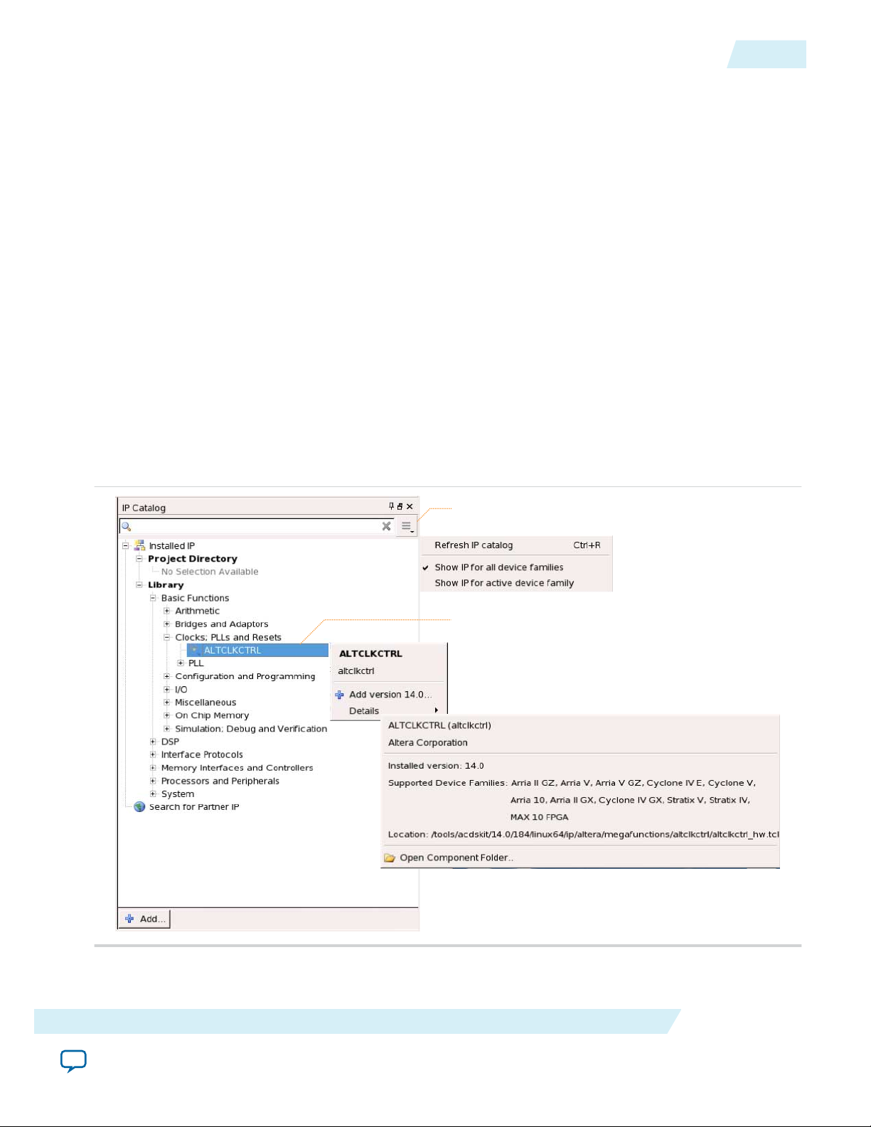
Search and filter IP for your target device
Double-click to customize, right-click for information
UG-01089
2014.12.17
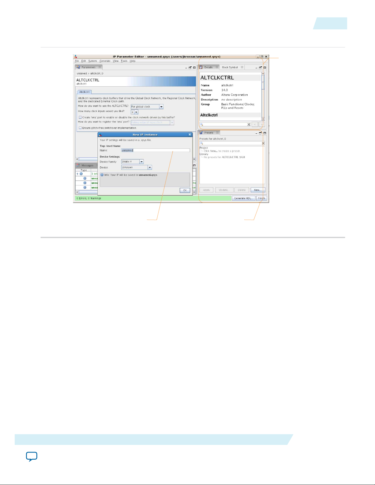
IP Catalog and Parameter Editor (replaces MegaWizard Plug-In Manager)
IP Catalog and Parameter Editor (replaces MegaWizard Plug-In Manager)
The Quartus II IP Catalog (Tools > IP Catalog) and parameter editor help you easily customize and
integrate IP cores into your project. You can use the IP Catalog and parameter editor to select, customize,
and generate files representing your custom IP variation.
Note: The IP Catalog (Tools > IP Catalog) and parameter editor replace the MegaWizard™ Plug-In
Manager for IP selection and parameterization, beginning in Quartus II software version 14.0. Use
the IP Catalog and parameter editor to locate and paramaterize Altera IP cores.
The IP Catalog lists IP cores available for your design. Double-click any IP core to launch the parameter
editor and generate files representing your IP variation. The parameter editor prompts you to specify an
IP variation name, optional ports, and output file generation options. The parameter editor generates a
top-level Qsys system file (.qsys) or Quartus II IP file (.qip) representing the IP core in your project. You
can also parameterize an IP variation without an open project.
Use the following features to help you quickly locate and select an IP core:
• Filter IP Catalog to Show IP for active device family or Show IP for all device families.
• Search to locate any full or partial IP core name in IP Catalog. Click Search for Partner IP, to access
partner IP information on the Altera website.
• Right-click an IP core name in IP Catalog to display details about supported devices, open the IP core's
installation folder, andor view links to documentation.
3
Figure 2: Quartus II IP Catalog
Note:
The IP Catalog is also available in Qsys (View > IP Catalog). The Qsys IP Catalog includes
exclusive system interconnect, video and image processing, and other system-level IP that are not
ALTDQ_DQS2 IP Core User Guide
Send Feedback
Altera Corporation
Page 4
View IP port
and parameter
details
Apply preset parameters for
specific applications
Specify your IP variation name
and target device
Legacy parameter
editors
4
Using the Parameter Editor
available in the Quartus II IP Catalog. For more information about using the Qsys IP Catalog, refer
to Creating a System with Qsys in the Quartus II Handbook.
Related Information
• Creating a System with Qsys
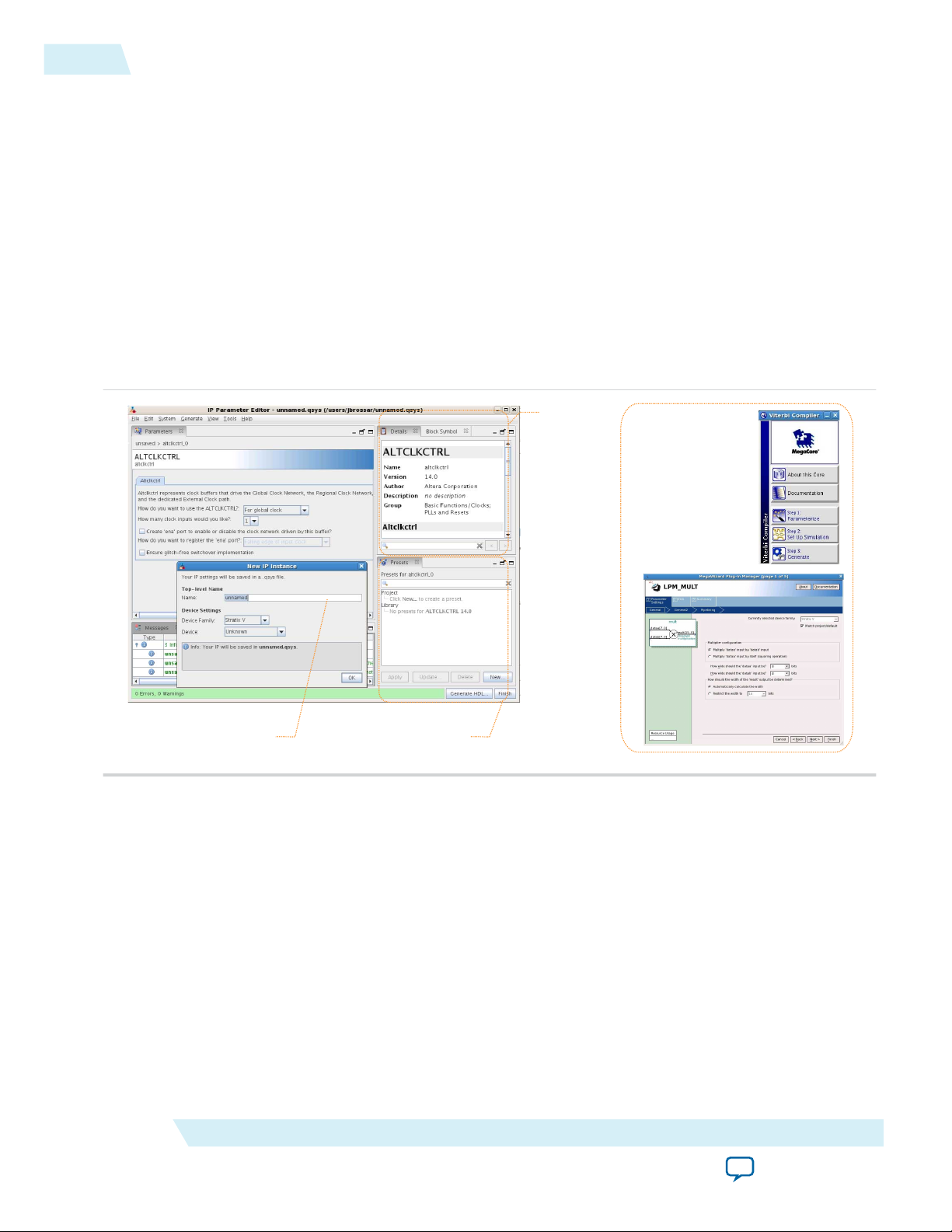
Using the Parameter Editor
The parameter editor helps you to configure IP core ports, parameters, and output file generation options.
• Use preset settings in the parameter editor (where provided) to instantly apply preset parameter values
for specific applications.
• View port and parameter descriptions, and links to documentation.
• Generate testbench systems or example designs (where provided).
Figure 3: IP Parameter Editors
UG-01089
2014.12.17
Adding IP Cores to IP Catalog
Altera Corporation
The IP Catalog automatically displays Altera IP cores found in the project directory, in the Altera
installation directory, and in the defined IP search path. The IP Catalog can include Altera-provided IP
components, third-party IP components, custom IP components that you provide, and previously
generated Qsys systems.
You can use the IP Search Path option (Tools > Options) to include custom and third-party IP
components in the IP Catalog. The IP Catalog displays all IP cores in the IP search path. The Quartus
software searches the directories listed in the IP search path for the following IP core files:
• Component Description File (_hw.tcl)—Defines a single IP core.
• IP Index File (.ipx)—Each .ipx file indexes a collection of available IP cores, or a reference to other
directories to search. In general, .ipx files facilitate faster searches.
The Quartus software searches some directories recursively and other directories only to a specific depth.
When the search is recursive, the search stops at any directory that contains an _hw.tcl or .ipx file.
ALTDQ_DQS2 IP Core User Guide
Send Feedback
Page 5
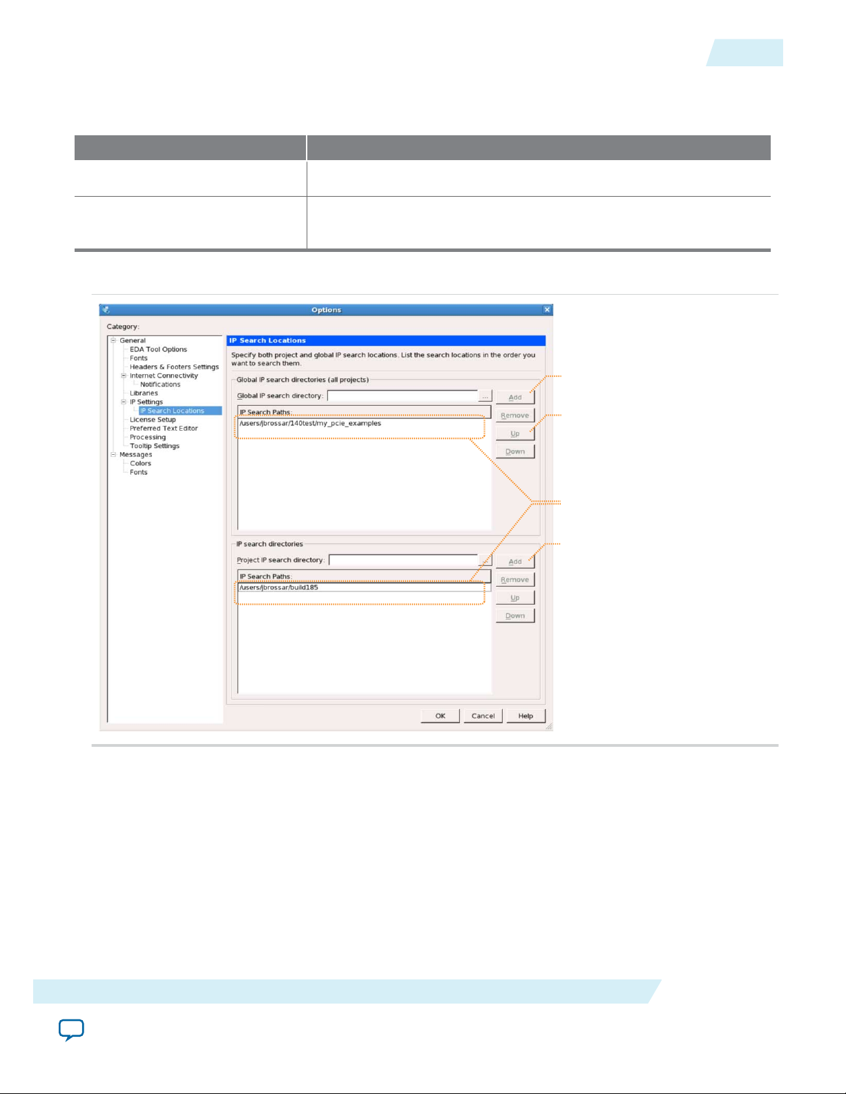
Adds new global IP search paths
Changes search path order
Adds new project-specific IP search paths
Lists current project and global search paths
UG-01089
2014.12.17
In the following list of search locations, a recursive descent is annotated by **. A single * signifies any file.
Table 1: IP Search Locations
Location Description
Adding IP Cores to IP Catalog
5
PROJECT_DIR/*
PROJECT_DIR/ip/**/*
Finds IP components and index files in the Quartus project directory.
Finds IP components and index files in any subdirectory of the /ip
subdirectory of the Quartus project directory.
Figure 4: Specifying IP Search Locations
If the Quartus software recognizes two IP cores with the same name, the following search path precedence
rules determine the resolution of files:
1. Project directory.
2. Project database directory.
3. Project IP search path specified in IP Search Locations, or with the SEARCH_PATH assignment in the
Quartus Settings File ( .qsf) for the current project revision.
4. Global IP search path specified in IP Search Locations, or with the SEARCH_PATH assignment in the
quartus2.ini file.
5. Quartus software libraries directory, such as <Quartus Installation>\libraries.
ALTDQ_DQS2 IP Core User Guide
Send Feedback
Altera Corporation
Page 6

6
Specifying IP Core Parameters and Options
Note: If you add a component to the search path, you must refresh your system by clicking File > Refresh
to update the IP Catalog.
Specifying IP Core Parameters and Options
The parameter editor GUI allows you to quickly configure your custom IP variation. You specify IP core
options and parameters in the Quartus II software.
1. In the IP Catalog (Tools > IP Catalog), locate and double-click the name of the IP core to customize.
The parameter editor appears.
2. Specify a top-level name for your custom IP variation. The parameter editor saves the IP variation
settings in a file named <your_ip>.qsys. Click OK.
3. Specify the parameters and options for your IP variation in the parameter editor, including one or
more of the following. Refer to your IP core user guide for information about specific IP core
parameters.
• Optionally select preset parameter values if provided for your IP core. Presets specify initial
parameter values for specific applications.
• Specify parameters defining the IP core functionality, port configurations, and device-specific
features.
• Specify options for processing the IP core files in other EDA tools.
4. Click Generate HDL, the Generation dialog box appears.
5. Specify output file generation options, and then click Generate. The IP variation files generate
according to your specifications.
6. To generate a simulation testbench, click Generate > Generate Testbench System.
7. To generate an HDL instantiation template that you can copy and paste into your text editor, click
Generate > HDL Example.
8. Click Finish. The parameter editor adds the top-level .qsys file to the current project automatically. If
you are prompted to manually add the .qsys file to the project, click Project > Add/Remove Files in
Project to add the file.
9. After generating and instantiating your IP variation, make appropriate pin assignments to connect
ports.
UG-01089
2014.12.17
Altera Corporation
ALTDQ_DQS2 IP Core User Guide
Send Feedback
Page 7
View IP port
and parameter
details
Apply preset parameters for
specific applications
Specify your IP variation name
and target device
UG-01089
2014.12.17
Figure 5: IP Parameter Editor
Files Generated for Altera IP Cores (version 14.0 and previous)
7
Files Generated for Altera IP Cores (version 14.0 and previous)
The Quartus II software version 14.0 and previous generates the following output for your IP core.
ALTDQ_DQS2 IP Core User Guide
Send Feedback
Altera Corporation
Page 8

Notes:
1. If supported and enabled for your IP variation
2. If functional simulation models are generated
<Project Directory>
<your_ip>_sim
1
<Altera IP>_instance.vo - IPFS model
2
<simulator_vendor>
<simulator setup scripts>
<your_ip>.qip - Quartus II IP integration file
<your_ip>.sip - Lists files for simulation
<your_ip>_testbench or _example - Testbench or example
1
<your_ip>.v, .sv. or .vhd - Top-level IP synthesis file
<AlteraIP_name>_instance
<your_ip>_syn.v or .vhd - Timing & resource estimation netlist
1
<your_ip>.cmp - VHDL component declaration file
<your_ip>.bsf - Block symbol schematic file
<your_ip> - IP core synthesis files
<your_ip>.sv, .v, or .vhd - HDL synthesis files
<your_ip>.sdc - Timing constraints file
<your_ip>.ppf - XML I/O pin information file
<your_ip>.spd - Combines individual simulation scripts
1
<your_ip>_sim.f - Refers to simulation models and scripts
1
8
Upgrading IP Cores
Figure 6: IP Core Generated Files
UG-01089
2014.12.17
Upgrading IP Cores
IP core variants generated with a previous version of the Quartus II software may require upgrading
before use in the current version of the Quartus II software. Click Project > Upgrade IP Components to
identify and upgrade IP core variants.
The Upgrade IP Components dialog box provides instructions when IP upgrade is required, optional, or
unsupported for specific IP cores in your design. You must upgrade IP cores that require it before you can
compile the IP variation in the current version of the Quartus II software. Many Altera IP cores support
automatic upgrade.
The upgrade process renames and preserves the existing variation file (.v, .sv, or .vhd) as <my_variant>_
BAK.v, .sv, .vhd in the project directory.
Altera Corporation
ALTDQ_DQS2 IP Core User Guide
Send Feedback
Page 9

UG-01089
2014.12.17
Table 2: IP Core Upgrade Status
IP Core Status Corrective Action
Upgrading IP Cores
9
Required Upgrade IP
Components
Optional Upgrade IP
Components
You must upgrade the IP variation before compiling in the current version of
the Quartus II software.
Upgrade is optional for this IP variation in the current version of the Quartus
II software. You can upgrade this IP variation to take advantage of the latest
development of this IP core. Alternatively you can retain previous IP core
characteristics by declining to upgrade.
Upgrade Unsupported Upgrade of the IP variation is not supported in the current version of the
Quartus II software due to IP core end of life or incompatibility with the
current version of the Quartus II software. You are prompted to replace the
obsolete IP core with a current equivalent IP core from the IP Catalog.
Before you begin
• Archive the Quartus II project containing outdated IP cores in the original version of the Quartus II
software: Click Project > Archive Project to save the project in your previous version of the Quartus II
software. This archive preserves your original design source and project files.
• Restore the archived project in the latest version of the Quartus II software: Click Project > Restore
Archived Project. Click OK if prompted to change to a supported device or overwrite the project
database. File paths in the archive must be relative to the project directory. File paths in the archive
must reference the IP variation .v or .vhd file or .qsys file (not the .qip file).
1. In the latest version of the Quartus II software, open the Quartus II project containing an outdated IP
core variation. The Upgrade IP Components dialog automatically displays the status of IP cores in
your project, along with instructions for upgrading each core. Click Project > Upgrade IP
Components to access this dialog box manually.
2. To simultaneously upgrade all IP cores that support automatic upgrade, click Perform Automatic
Upgrade. The Status and Version columns update when upgrade is complete. Example designs
provided with any Altera IP core regenerate automatically whenever you upgrade the IP core.
ALTDQ_DQS2 IP Core User Guide
Altera Corporation
Send Feedback
Page 10
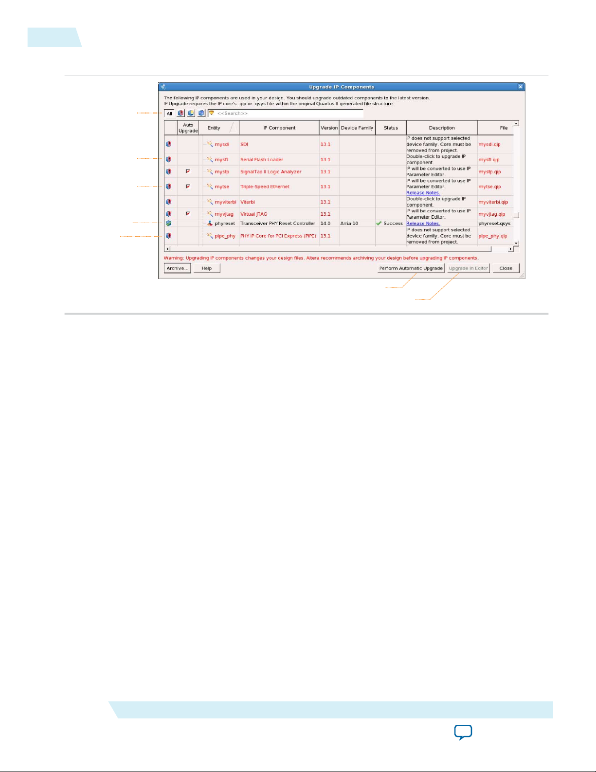
Displays upgrade
status for all IP cores
in the Project
Upgrades all IP core that support “Auto Upgrade”
Upgrades individual IP cores unsupported by “Auto Upgrade”
Checked IP cores
support “Auto Upgrade”
Successful
“Auto Upgrade”
Upgrade
unavailable
Double-click to
individually migrate
10
Upgrading IP Cores
Figure 7: Upgrading IP Cores
UG-01089
2014.12.17
Example 1: Upgrading IP Cores at the Command Line
You can upgrade IP cores that support auto upgrade at the command line. IP cores that do not
support automatic upgrade do not support command line upgrade.
• To upgrade a single IP core that supports auto-upgrade, type the following command:
quartus_sh –ip_upgrade –variation_files <my_ip_filepath/my_ip>.<hdl>
<qii_project>
Example:
quartus_sh -ip_upgrade -variation_files mega/pll25.v hps_testx
• To simultaneously upgrade multiple IP cores that support auto-upgrade, type the following
command:
quartus_sh –ip_upgrade –variation_files “<my_ip_filepath/my_ip1>.<hdl>;
<my_ip_filepath/my_ip2>.<hdl>” <qii_project>
Example:
quartus_sh -ip_upgrade -variation_files "mega/pll_tx2.v;mega/pll3.v"
hps_testx
Note:
IP cores older than Quartus II software version 12.0 do not support upgrade.
Altera verifies that the current version of the Quartus II software compiles the
previous version of each IP core. The Altera IP Release Notes reports any verifica‐
tion exceptions for Altera IP cores. Altera does not verify compilation for IP cores
older than the previous two releases.
Altera Corporation
ALTDQ_DQS2 IP Core User Guide
Send Feedback
Page 11

UG-01089
2014.12.17
Related Information
Altera IP Release Notes
ALTDQ_DQS2 Parameter Settings
You can instantiate and parameterize using the IP Catalog and parameter editor GUI, or the ip-generate
command through the command-line interface (CLI).
The following table lists the ALTDQ_DQS2 parameter settings.
Table 3: ALTDQ_DQS2 Parameter Settings
ALTDQ_DQS2 Parameter Settings
11
Parameter Editor GUI Setting
Name
Legal Values
General Settings
Pin width 1 to 36
Pin type input
output
bidir
Extra output-only
0 – 36
pins
CLI Parameter
Name
PIN_WIDTH 1 to 36
PIN_TYPE
EXTRA_OUTPUT_WIDTH 0 to 36
Legal
Values
input
output
bidir
(1)
Description
This setting specifies the
number of data (DQ) pins
to make as part of this
DQS group.
The default value is 9 (9).
This setting specifies the
direction of the data pins
(input, output, or bidirec‐
tional).
The default value is bidir
(bidir).
This setting specifies the
extra output pins that you
need as part of a DQS
group.
(1)
All CLI parameter values are type string, therefore you must enclose the values in double quotes.
ALTDQ_DQS2 IP Core User Guide
Send Feedback
A common use for this
setting is to add datamask
pins.
The default value is 0 (0).
Altera Corporation
Page 12

12
ALTDQ_DQS2 Parameter Settings
UG-01089
2014.12.17
Parameter Editor GUI Setting
Name
Legal Values
Memory frequency 1–1068
Use DLL Offset
—
Control
Enable hard FIFOs —
CLI Parameter
Name
INPUT_FREQ 120–1068
USE_OFFSET_CTRL
USE_HARD_FIFOS
Legal
Values
true
false
true
false
(1)
Description
This setting specifies the
full-rate clock frequency
of the incoming DQS
group signal from the
external device in MHz.
The default value is
300 MHz (300).
This setting enables
dynamic control of the
DLL offset.
Altera recommends using
this setting for test
purposes only. For DQS
data capture calibration,
use the D1, D2, D3, and
D4 delay chains.
This setting enables the
hard FIFOs (read FIFO for
Stratix V devices and read
FIFO, latency shifter FIFO
and data valid FIFO for
Arria V and Cyclone V
devices) as part of the
ALTDQ_DQS2 IP core.
Use Capture Clock
to clock the read
Side of the Hard
VFIFO
Enable dual write
clocks
(1)
All CLI parameter values are type string, therefore you must enclose the values in double quotes.
Altera Corporation
—
—
USE_DQSIN_FOR_
VFIFO_READ
DUAL_WRITE_CLOCK
true
false
true
false
Turn on this setting when
you use the hard data valid
FIFO and when the
capture clock is not gated.
This setting is available
only for Arria V and
Cyclone V devices.
This setting enables the
use of separate output
clocks for data and strobe.
This setting is disabled by
default for Arria V and
Cyclone V devices.
ALTDQ_DQS2 IP Core User Guide
Send Feedback
Page 13
UG-01089
2014.12.17
ALTDQ_DQS2 Parameter Settings
13
Parameter Editor GUI Setting
Name
Use dynamic
Legal Values
—
configuration scan
chains
Output Path
CLI Parameter
Name
USE_DYNAMIC_CONFIG
Legal
Values
true
false
Description
(1)
This setting enables
run-time configuration of
multiple delay chains,
phase shifts, and transfer
registers.
Requires a correctly
formatted bitstream.
For more information,
refer to DQS Configura‐
tion Block Bit Sequence
for Arria V GZ and
Stratix V Devices on page
42 and DQS Configura‐
tion Block Bit Sequence
for Arria V and Cyclone
V Devices on page 56.
Use half-rate
output path
Use output phase
alignment blocks
—
—
HALF_RATE_OUTPUT
USE_OUTPUT_PHASE_
ALIGNMENT
true
false
true
false
This setting doubles the
width of the data bus on
the FPGA side and clocks
the FPGA side interface
using the half-rate clock
input.
If this setting is enabled,
drive the hr_clock_in
port with the half-rate
clock signal.
When enabling hard read
FIFO in a Stratix V device,
you must set this
parameter to true.
This setting is enabled by
default.
This setting enables phase
shift on the output path
based on the delay settings
from the DLL.
This setting is disabled by
default.
(1)
All CLI parameter values are type string, therefore you must enclose the values in double quotes.
ALTDQ_DQS2 IP Core User Guide
Send Feedback
Altera Corporation
Page 14

14
ALTDQ_DQS2 Parameter Settings
UG-01089
2014.12.17
Parameter Editor GUI Setting
Name
Legal Values
Capture Strobe
Capture strobe
type
Single
Differential
Complemen‐
tary
Use inverted
—
capture strobe
CLI Parameter
Name
CAPTURE_STROBE_TYPE
INVERT_CAPTURE_
STROBE
Legal
(1)
Values
single
differential
complementary
true
false
Description
This setting specifies the
type of capture strobe
(DQS signal from the
external device).
The default value is Single
(single).
When enabled, this
parameter captures data
with an inverted capture
strobe.
Strobe inversion occurs
from dqsbusout (an
output port from the DQS
delay chain block) to the
clock input of the DDIO_
IN block.
DQS phase shift 0 degrees
45 degrees
90 degrees
135 degrees
Use capture strobe
—
enable block
DQS_PHASE_SETTING
USE_DQS_ENABLE
0
1
2
3
true
false
This setting is enabled by
default.
This setting specifies the
phase shift value for the
DQS delay chain to shift
the incoming strobe in the
data valid window during
read and write operations.
The default value is 90
degrees (2).
This setting is for Stratix V
devices only.
This setting enables the
capture strobe enable
block, which allows
control over the preamble
state of the capture strobe.
This setting is disabled by
default.
(1)
All CLI parameter values are type string, therefore you must enclose the values in double quotes.
Altera Corporation
ALTDQ_DQS2 IP Core User Guide
Send Feedback
Page 15

UG-01089
2014.12.17
ALTDQ_DQS2 Parameter Settings
15
Parameter Editor GUI Setting
Name
Treat the capture
Legal Values
—
strobe enable as a
half-rate signal
DQS enable phase
setting
0 degrees
45 degrees
90 degrees
135 degrees
Output Strobe
Generate output
—
strobe
CLI Parameter
Name
USE_HALF_RATE_DQS_
ENABLE
DQS_ENABLE_PHASE_
SETTING
USE_OUTPUT_STROBE
Legal
Values
true
false
0
1
2
3
true
false
Description
(1)
This setting doubles the
width of the capture
strobe enable bus on the
FPGA side and clocks the
FPGA side interface using
the half-rate clock input.
This setting specifies the
value of phase shift to shift
the full-rate clock signal
that drives the capture
strobe enable block.
The default value is 0
degrees (0).
This setting generates an
output strobe signal based
on the OE signal and the
full-rate clock. This setting
is enabled by default.
Make capture
strobe bidirec‐
tional
—
USE_BIDIR_STROBE
true
false
This setting enables the
bidirectional capture
strobe (capture strobe and
output strobe is on the
same port).
This setting is disabled by
default.
Differential/
complementary
output strobe
—
DIFFERENTIAL_
OUTPUT_STROBE
true
false
This setting enables either
the differential or
complementary output
strobe.
This setting is disabled by
default.
(1)
All CLI parameter values are type string, therefore you must enclose the values in double quotes.
ALTDQ_DQS2 IP Core User Guide
Send Feedback
Altera Corporation
Page 16

16
ALTDQ_DQS2 Parameter Settings
UG-01089
2014.12.17
Parameter Editor GUI Setting
Name
Use reset signal to
Legal Values
—
stop output strobe
OCT Source Output Strobe
Enable
Data Write
Enable
Dedicated
OCT Enable
CLI Parameter
Name
USE_OUTPUT_STROBE_
RESET
OCT_SOURCE
Legal
Values
true
false
0
1
2
Description
(1)
This setting stops the
unidirectional output
strobe using a userprovided reset signal. The
core_clock_in and the
reset_n_core_clock_in
signals are required.
This setting specifies the
type of input signal to
toggle the OCT control:
• Output Strobe Enable
—Uses the output_
strobe_ena input as
the OCT control signal.
• Data Write Enable—
Uses the write_oe_in
input as the OCT
control signal.
• Dedicated OCT
Enable—Adds a oct_
ena_in input to the
interface, which is used
as the OCT control
signal.
(1)
All CLI parameter values are type string, therefore you must enclose the values in double quotes.
Altera Corporation
The availability of the
Output Strobe Enable,
Data Write Enable,and
Dedicated OCT Enable
are dependent on PIN_
TYPE and USE_BIDIR_
STROBE parameters.
Default value is Data
Write Enable.
ALTDQ_DQS2 IP Core User Guide
Send Feedback
Page 17
UG-01089
2014.12.17
ALTDQ_DQS2 Data Paths
17
Parameter Editor GUI Setting
Name
Legal Values
Preamble type high
low
none
CLI Parameter
Name
PREAMBLE_TYPE
Legal
Values
high
low
none
Description
(1)
This setting sets the DQS
preamble to high (DDR3),
low (DDR2), or none:
• When you select low
and the strobe is
bidirectional, the
output strobe is held
low for the first full
rate cycle.
• When you select high
or none, the strobe is
driven high for the first
full rate cycle.
• Default value is low.
Note:
The ALTDQ_
DQS2 IP core
does not
support DQS
tracking.
Related Information
• DQS Configuration Block Bit Sequence for Arria V and Cyclone V Devices on page 56
• DQS Configuration Block Bit Sequence for Arria V GZ and Stratix V Devices on page 42
• IP-Generate Command on page 96
ALTDQ_DQS2 Data Paths
Describes the read and write data paths and using other IP cores with the ALTDQ_DQS2 IP core.
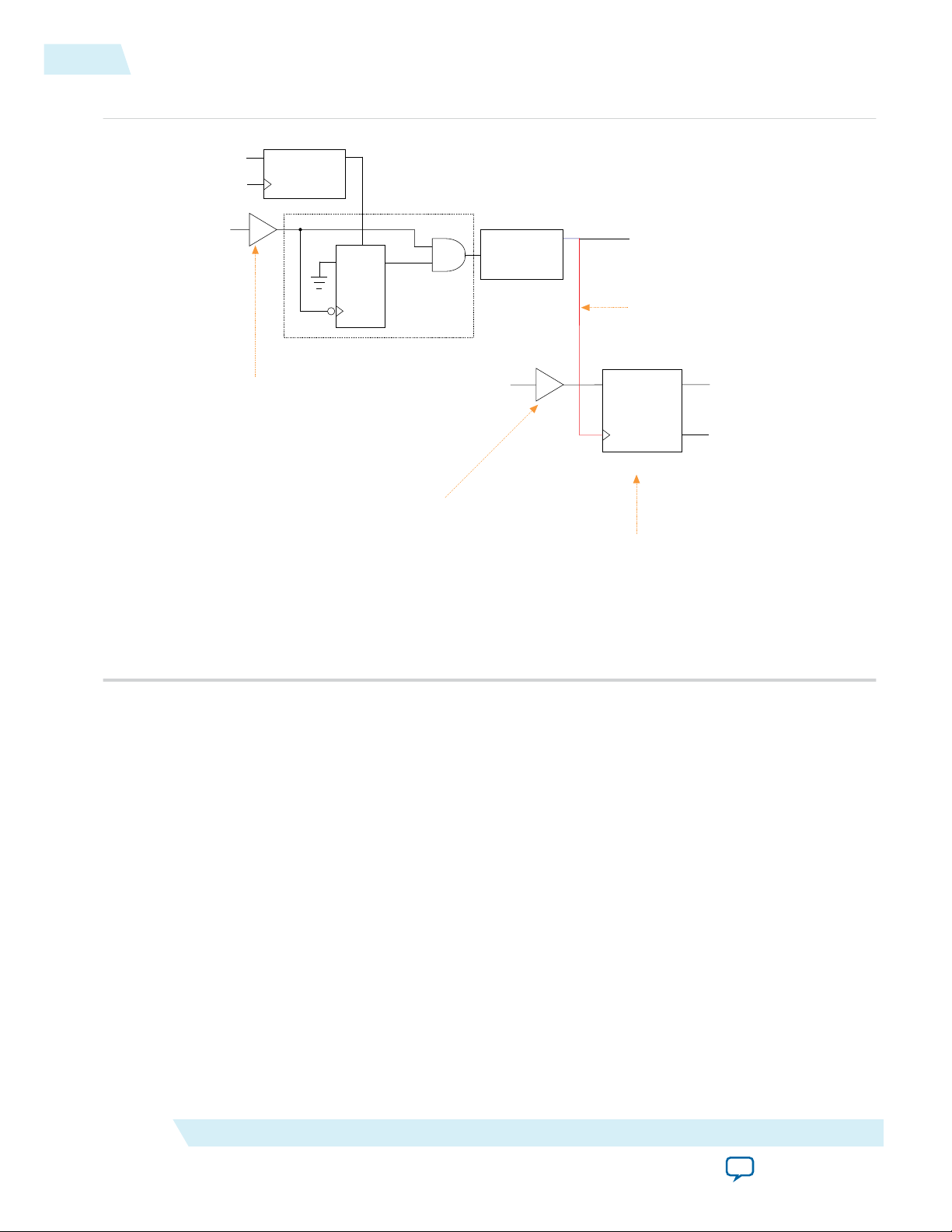
DQ and DQS Input Path
The DQ and DQS input paths receive the DQ and DQS signals from the external device during read
operations.
DQ and DQS Input Paths for Stratix V Devices
The following figure shows the input paths where x = 0 to (n-1) and n = the number of DQ pins.
(1)
All CLI parameter values are type string, therefore you must enclose the values in double quotes.
ALTDQ_DQS2 IP Core User Guide
Send Feedback
Altera Corporation
Page 18
capture_strobe_ena
PRE
D
Q
IN
LO
strobe_ena_clock_in
DQS Enable Control
DQS Delay Chain
HI
DQSIN
DQSBUSOUT
IN
OUT
capture_strobe_in
DQS Enable
read_data_in[x]
capture_strobe_out
read_data_out[x]
read_data_out[n+x]
(from DQS pin)
(from DQ pin)
DDIO_IN
You can use the DDIO_IN block with a soft or
hard read FIFO in Stratix V devices. However,
you can use this block with only a hard read
FIFO in Arria V and Cyclone V devices.
When the hard read FIFO block is not present,
the DQ and DQS path ends at the DDIO_IN
block.
For bidirectional DQS, the input of the
buffer connects to the strobe_io port.
For bidirectional DQ, the input of the buffer
connects to the read_write_data_io[x] port.
Optional inversion occurs from dqsbusout
(output port from the DQS delay chain block) to
the clock input of the DDIO_IN block.
CLK
18
Data Input Path for Arria V, Cyclone V, and Stratix V Devices
Figure 8: DQ and DQS Input Paths for Stratix V Devices
UG-01089
2014.12.17
Data Input Path for Arria V, Cyclone V, and Stratix V Devices
Altera Corporation
Note: For more information about the DQ and DQS input path with a hard read FIFO block, refer to
The DQ and DQS input paths in Arria V and Cyclone V devices are the same, except for an additional
read FIFO block to implement the second-stage rate conversion DDIO. The high-speed 4 x 8 read FIFO,
Figure 9 and Figure 10.
clocked by the DQS clock, implements the half-rate to full-rate conversion, if necessary.
The following figure shows the data input path (when you enable the hard read FIFO) for Arria V,
Cyclone V, and Stratix V devices.
ALTDQ_DQS2 IP Core User Guide
Send Feedback
Page 19
DATAIN
Delay
Chain
DDIO
In
FIFO REN Logic
DATAOUT[0]
DATAOUT[1]
DATAOUT[2]
DATAOUT[3]
HR or FR Clock
DQS from DQS Logic
FIFO WREN
Logic
Read
FIFO
WREN REN
This figure is applicable to Stratix V devices because Stratix V devices support optional hard read FIFO.
UG-01089
2014.12.17
Figure 9: Data Input Path for Arria V, Cyclone V, and Stratix V Devices
Blocks in DQ and DQS Data Input Path
The following table lists the blocks in the DQ and DQS input paths.
Blocks in DQ and DQS Data Input Path
19
Table 4: Blocks in DQ and DQS Input Path
Block Name Description
DQS enable • Represents the AND-gate control on the DQS input that grounds
the DQS input strobe when the strobe goes to Hi-Z after a DDR
read postamble. The DQS enable block enables the registers to
allow enough time for the DQS delay settings to travel from the
DQS phase-shift circuitry or core logic to all the DQS logic blocks
before the next change.
• For more information about the DQS enable block, refer to the
“Update Enable Circuitry” in the External Memory Interfaces
chapter in the respective device handbook.
DQS enable control • Represents the circuitry that controls the DQS enable block. A
DQS enable control block controls each DQS enable block.
• For more information about the DQS enable control block, refer
to the “DQS Postamble Circuitry” in the External Memory
Interfaces chapter in the respective device handbook.
DQS delay chain • Represents the delay chains that delay signals.
• For more information about the DQS delay chain block, refer to
“DQS Delay Chain” in the External Memory Interfaces chapter in
the respective device handbook.
ALTDQ_DQS2 IP Core User Guide
Send Feedback
Altera Corporation
Page 20
capture_strobe_ena[0]
DDIO
Out
FR Clock
capture_strobe_ena[1]
strobe_ena_hr_clock_in
vfifo_inc_wr_ptr
inc_wr_ptr
capture_strobe_in
Data Valid
FIFO
DQS Enable
Control
DQS Delay
Chain
DQS Clock Tree
These ports are 2-bit wide because the
DDIO_OUT block is driven by a half-rate
clock, allowing you to enable DQS during
a half-rate cycle.
The data valid FIFO is a hard FIFO
in Arria V and Cyclone V devices.
Read FIFO
Write Enable
20
DQS Logic
DQS Logic
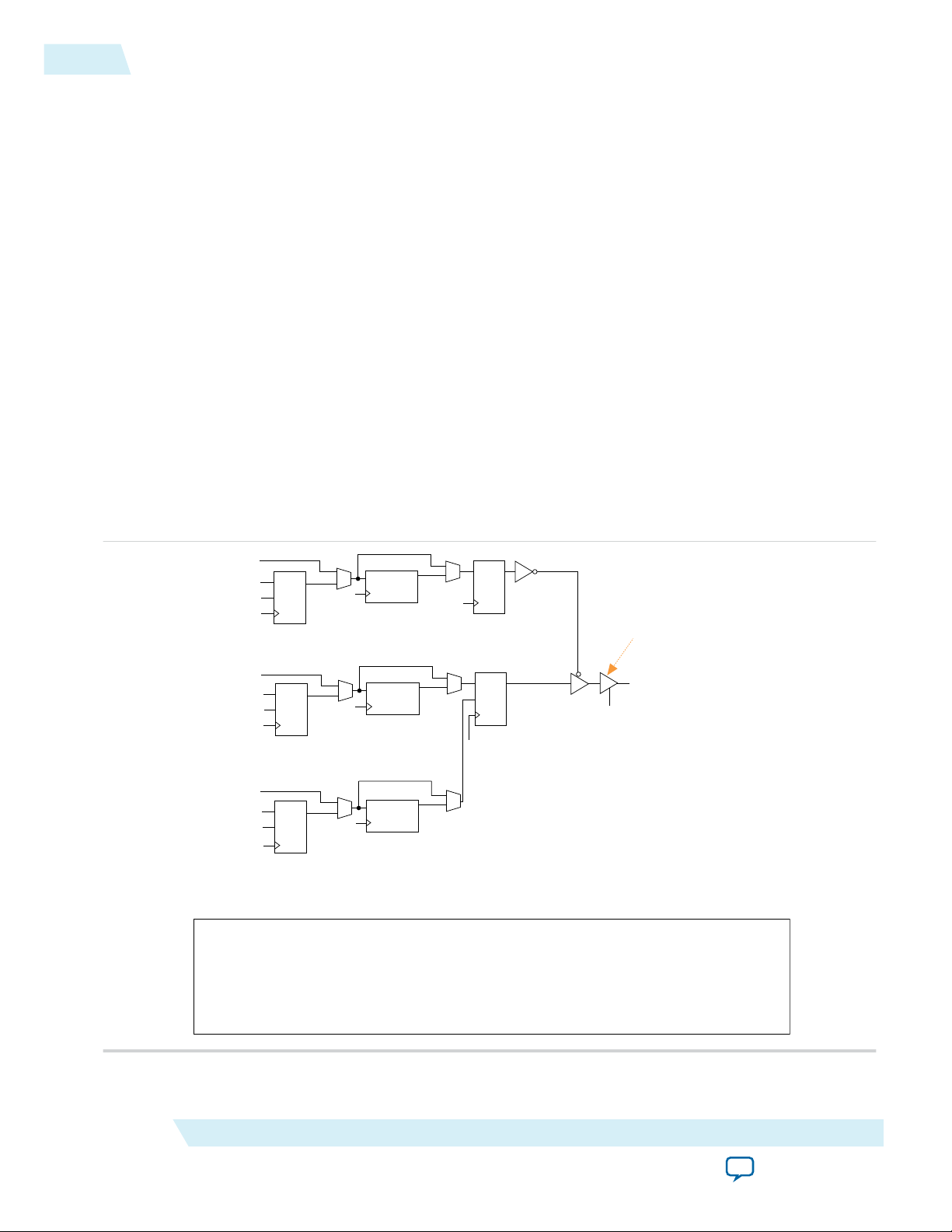
The DQS input path in Arria V and Cyclone V devices has the following differences from Stratix V and
earlier versions of the device families:
• A data valid FIFO delays the DQS enable path by up to 16 full-rate cycles. During a required calibra‐
tion process, you can increase the unknown delay, which the data valid FIFO implements, by 1, by
pulsing the INC_WR_PTR port. The delay wraps around after 16 increments.
• The DQS delay chain implements a static non-programmable phase shift of 90°.
The following figure shows the DQS input path in Arria V and Cyclone V devices.
Figure 10: DQS Input Path in Arria V and Cyclone V Devices
UG-01089
2014.12.17
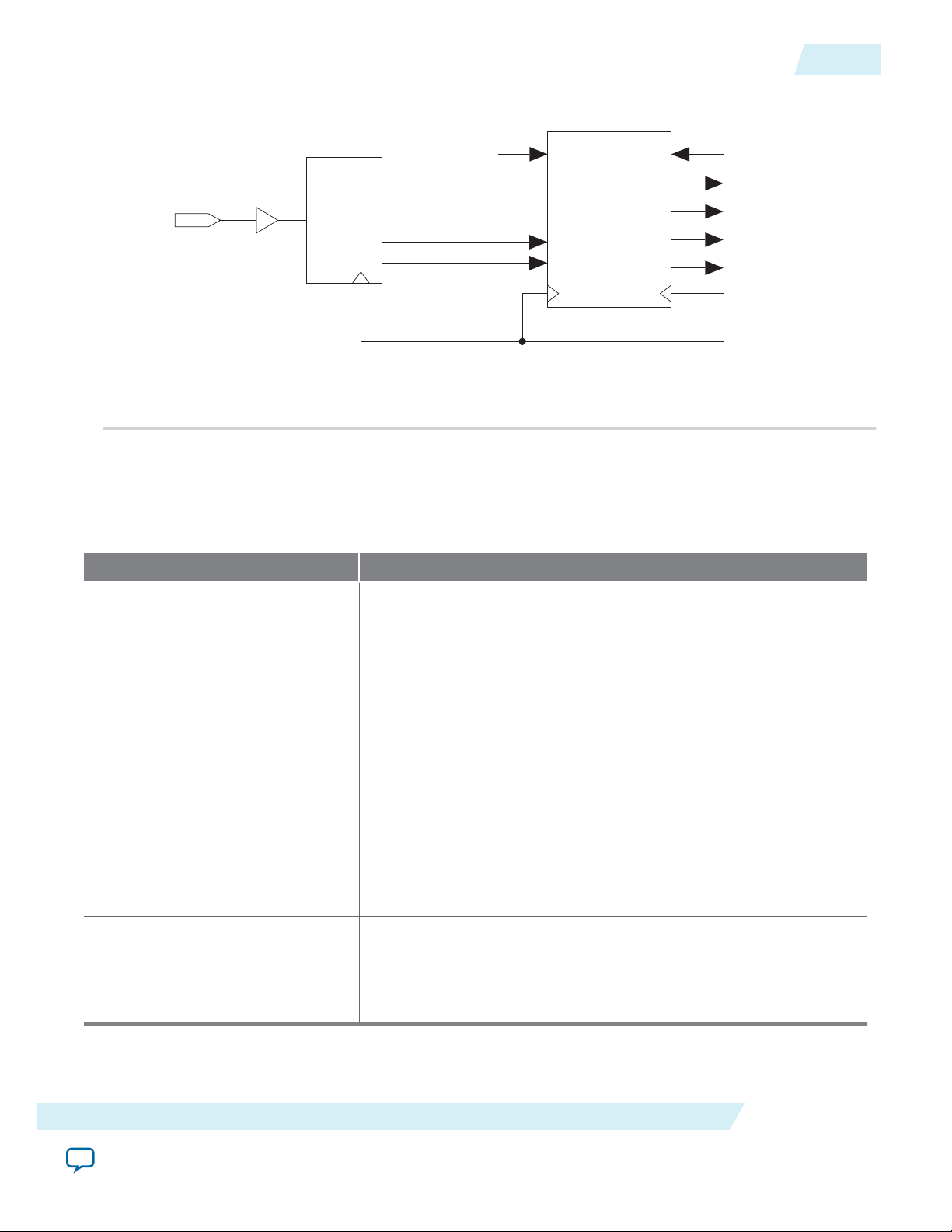
Capture DDIO to Read FIFO Path
The capture DDIO block captures input data (DQ) on the rising and falling edges of the capture clock or
strobe (DQS).
For Stratix V devices, the capture DDIO block feeds the hard read FIFO or bypasses the hard read FIFO
and goes directly to the core. If the capture DDIO block connects directly to the core, the data is
transmitted at full rate. For protocols with bidirectional DQS, only an exact number of DQS edge is
available for both capturing data in the capture DDIO block and then either in the read FIFO or in the
core. The data transfer from the capture DDIO block and the next stage is referred to as zero-cycle
transfer. This means that the transfer must happen on the same clock edge.
The hard read FIFO always changes the data rate from full-rate to half-rate, so if you choose to use fullrate, then you cannot use the Read FIFO.
For Arria V and Cyclone V devices, the capture DDIO block to Read FIFO path is similar, with the
following exceptions:
• The read FIFO must always be used and cannot be bypassed.
• The read FIFO supports both half-rate and full-rate.
For Arria V, Cyclone V, and Stratix V devices, the hard read FIFO implements the functionality of a
generic asynchronous FIFO. You can locate the hard read FIFO in a true dual-ported RAM. Data is
written to the write side of the DQS clock domain and read from the read side of the core clock domain.
For Arria V and Cyclone V devices, the core clock domain can run at half the frequency and implements a
full-rate to half-rate transformation. You can use the write enable and read enable signals to control when
to write and read data from the read FIFO. The same signal controls the increment of the write and read
Altera Corporation
ALTDQ_DQS2 IP Core User Guide
Send Feedback
Page 21
The read FIFO block is a hard FIFO in Arria V,
Cyclone V, and Stratix V devices. The latency
shifter FIFO and data valid FIFO are hard
FIFO in Arria V and Cyclone V devices.
Read
FIFO
DOUT
DIN
REN WREN
Latency
Shifter
FIFO
Data
Valid
FIFO
Data to Core Data from DQ
To DQS Enable
Read Data Enable from Core
UG-01089
2014.12.17
FIFO Control
pointers. For protocols using a bidirectional strobe, the write enable signal is tied to VCC and DQS
gating/ungating implements the write enable functionality.
For Arria V and Cyclone V devices, the hard data valid FIFO internally generates the write enable (or
gating/ungating) signal, while the hard latency FIFO internally generates the read enable signal.
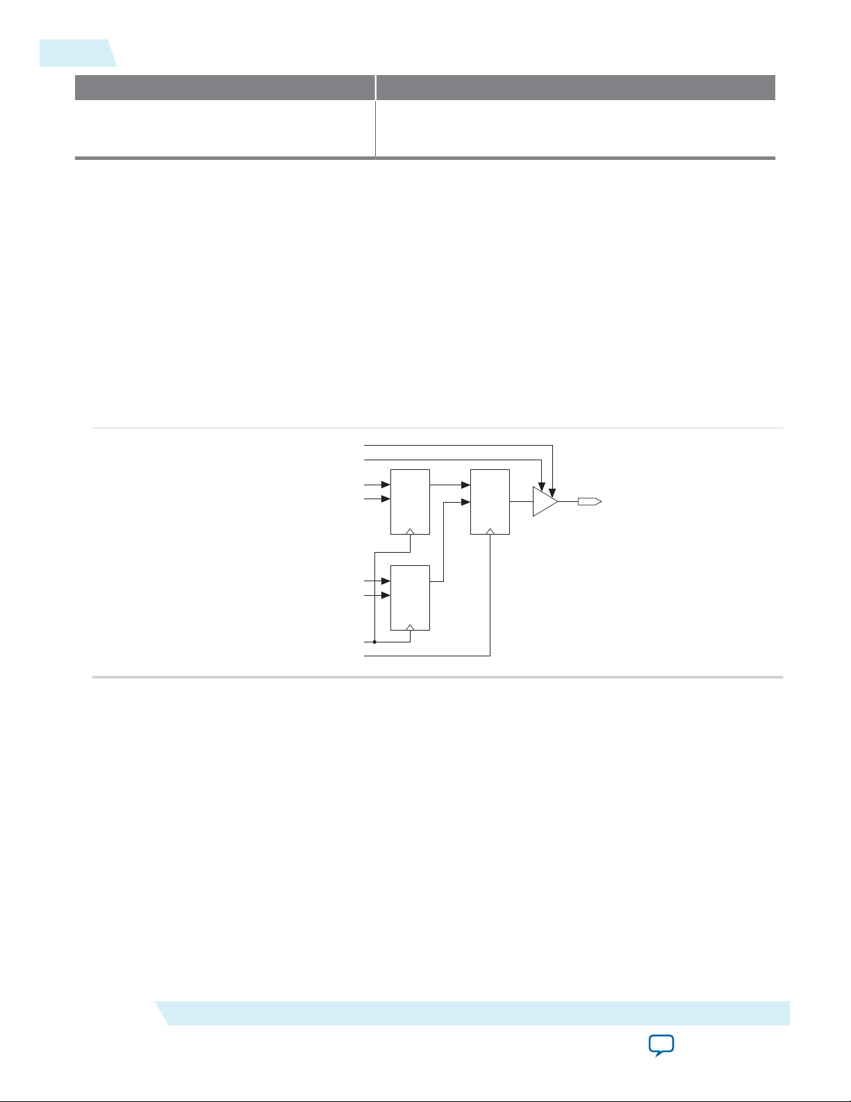
FIFO Control
For Arria V and Cyclone V devices, in addition to the read FIFO and the data valid FIFO, the location of
the latency shifter FIFO is in each DQS group. The latency shifter FIFO takes in a read-enable command
from the core and implements a programmable latency of up to 32 cycles before feeding into the readenable port of the read FIFO.
You can use the output of the data valid FIFO to perform the following tasks:
• To ungate the DQS logic when a strobe signal is capturing the data. In this case, the write-enable port
must always be '1' on the read FIFO.
• To enable the read FIFO write-enable port when a clock is in use.
The following figure shows the three FIFOs interconnection.
Figure 11: Data Valid FIFO, Latency Shifter FIFO, and Read FIFO Interconnection
21
ALTDQ_DQS2 IP Core User Guide
Send Feedback
When a read command is sent to the memory device, a read-data-enable token is pushed through the data
valid FIFO and the latency shifter FIFO. The data valid FIFO implements a latency equal to the read
command to data latency. When the token comes out of the data valid FIFO, the DQS signal is ungated.
The latency shifter FIFO then creates enough space between write and read pointers in the read FIFO to
ensure that the data read on the read side is correct. If the read FIFO is read at half-rate, the read FIFO
also implements a full-rate to half-rate conversion.
Altera Corporation
Page 22
write_oe_in[2x]
hr_clock_in
datain
dataout
LO
OUT
write_oe_in[2x+1]
D
Q
write_data_in[3n+x]
hr_clock_in
HI
OUT
write_data_in[n+x]
HI
OUT
hr_clock_in
write_data_in[2n+x]
datain
dataout
HI
Q
write_data_in[x]
LO
HI
Half-rate to
single-rate output
enable registers
Output phase
alignment registers
Alignment
clock
Write
clock
0
1
LO
0
1
datain
dataout
0
1
DDR output registers
Write
clock
Alignment
clock
write_data_out[x]
Half-rate to
single-rate
output registers
Alignment
clock
Half-rate to
single-rate
output registers
Output phase
alignment registers
Output phase
alignment registers
0
1
0
1
0
1
Series termination
control
LO
write_oe_in[x]
(to DQ pin)
write_data_in[x]
write_data_in[n+x]
DFF
Alignment
clock
Write
clock
Series termination
control
The alignment clock comes from the write-leveling delay chains. For more information, refer to “Leveling Circuitry”
section in the External Memory Interfaces in Stratix V Devices chapter in the Stratix V Device Handbook.
The write clock comes from the PLL or the write-leveling delay chains. For more information, refer to “Leveling
Circuitry” section in the External Memory Interfaces in Stratix V Devices chapter in the Stratix V Device Handbook.
The series termination control connects to the ALTOCT megafunction.
For bidirectional DQ, the output of the buffer
connects to the read_write_data_io[x] port.
22
DQ and DQS Output Path
The determination of the correct latencies to implement at each of these FIFOs is important and cannot
be done during compilation. When you attempt to implement your own custom memory solution, you
must also implement some form of calibration algorithm.
To determine if the data coming from the read FIFO is valid, you must implement the read data valid
latency in soft logic.
Related Information
UniPHY External Memory Interface Debug Toolkit
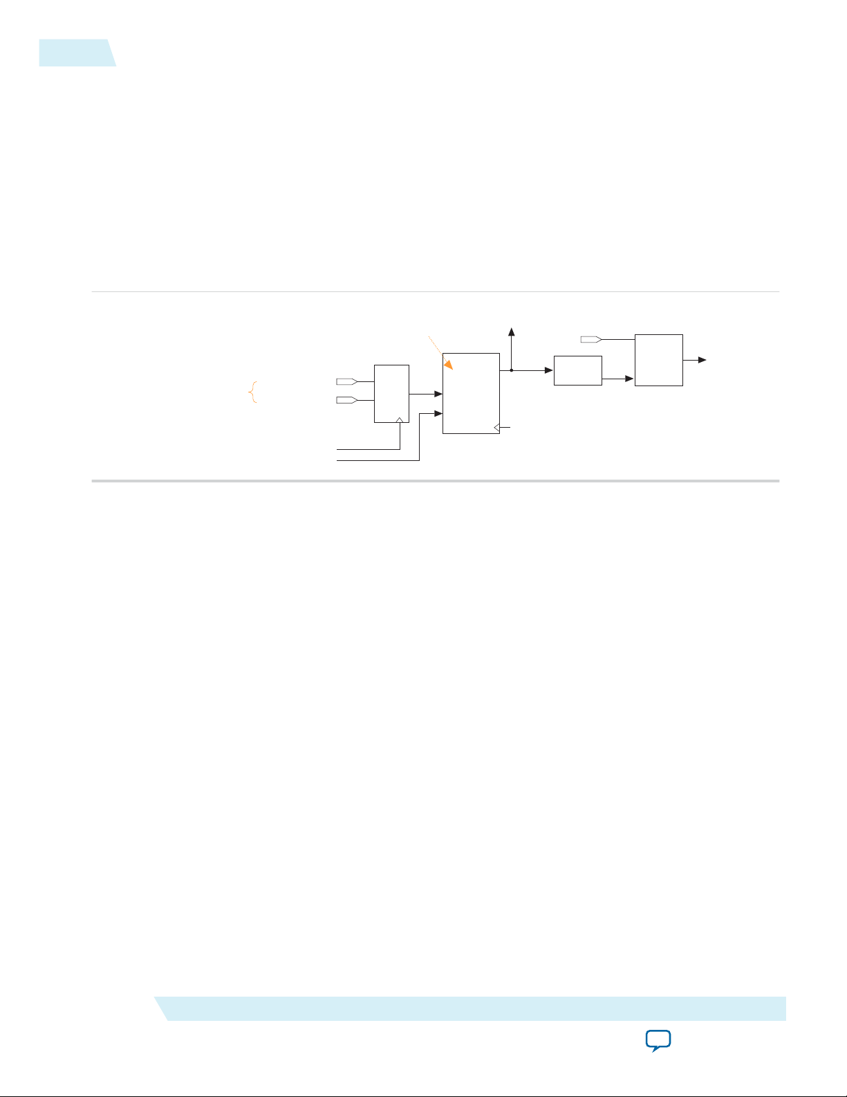
DQ and DQS Output Path
The DQ and DQS output path sends the DQ and DQS signal to the external device during write
operations.
DQ and DQS Output Path for Stratix V Devices
The following figure shows the output path where n = the number of DQ pins and x = 0 to (n-1). is only
applicable for Stratix V devices.
Note: This figure is only applicable for Stratix V devices. For Arria V and Cyclone V DQ and DQS output
path, refer to Figure 14.
UG-01089
2014.12.17
Figure 12: DQ and DQS Output Path for Stratix V Devices
Altera Corporation
ALTDQ_DQS2 IP Core User Guide
Send Feedback
Page 23
extra_write_data_in[3m+y]
hr_clock_in
datain
dataout
HI
OUT
extra_write_data_in[2m+y]
HI
OUT
hr_clock_in
extra_write_data_in[m+y]
datain
dataout
HI
OUT
extra_write_data_in[y]
LO
Half-rate to
single-rate output
enable registers
Output phase
alignment registers
Alignment
clock
0
1
Alignment
clock
Half-rate to
single-rate
output registers
Output phase
alignment registers
0
1
0
1
0
1
VCC
DDR output registers
extra_write_data_out[y]
Write clock
LO
LO
extra_write_data_in[y]
(to DQ pin)
Alignment
clock
Write clock
The alignment clock comes from the write-leveling delay chains.
The write clock comes from the PLL or the write-leveling delay chains.
UG-01089
2014.12.17
Blocks in DQ and DQS Output Path
The following figure shows the DQ and DQS output path for additional DQ pins usage, where y = 0 to
(m-1) and m= the number of DQ pins
Figure 13: DQ and DQS Output Path (for Additional DQ Pins Usage) for Stratix V Devices
23
Blocks in DQ and DQS Output Path
Table 5: Blocks in the DQ and DQS Output Path
ALTDQ_DQS2 IP Core User Guide
Related Information
• External Memory Interfaces in Stratix V Devices
The following table lists the blocks in the DQ and DQS output path.
Block Name Description
Half-rate to single-rate output enable
registers
Output phase alignment registers Represents the circuitry required to phase shift the DQ-
Represents a group of registers that convert half-rate data to
single-rate data.
output signals. Use this block for write-leveling purposes in
DDR3 SDRAM interfaces.
Altera Corporation
Send Feedback
Page 24
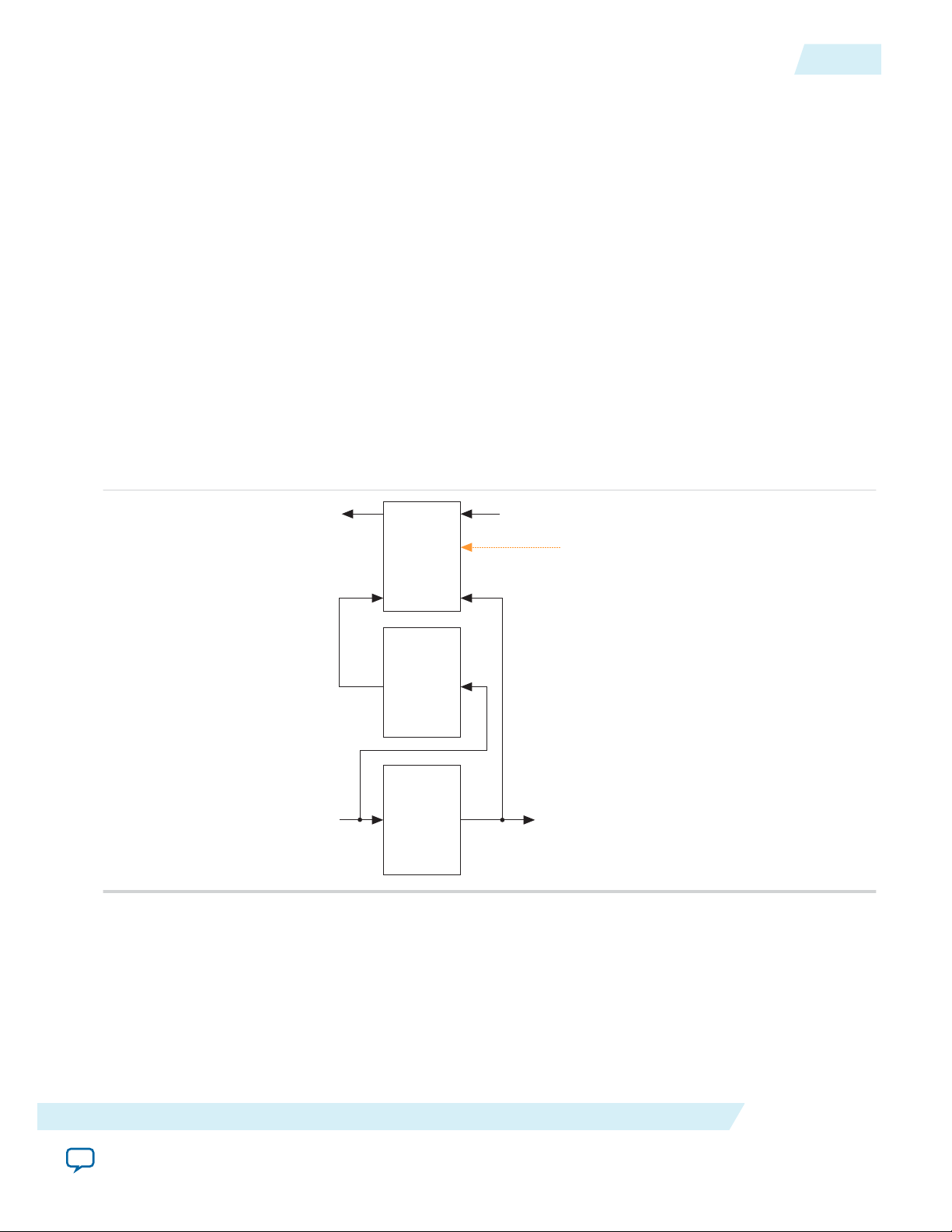
DATAOUT
DDIO
Out
DATAOUT[0]
DATAOUT[1]
DATAOUT[2]
DATAOUT[3]
DDIO
Out
DDIO
Out
CLK_HR
CLK_FR
OCT from DQS Logic
OE from Output Enable Path
24
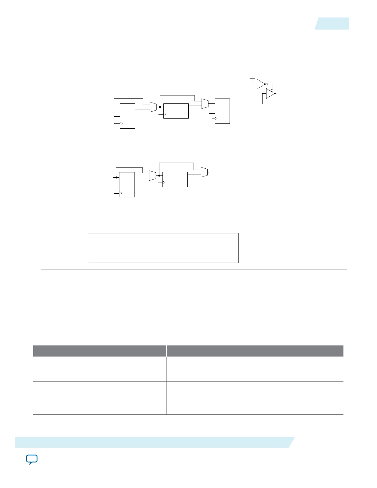
DQ and DQS Output Path for Arria V and Cyclone V Devices
Block Name Description
DDR output registers Represents the DDIO registers that transfer DDR signals
from the core to the DQ/DQS pins.
Related Information
• External Memory Interfaces in Arria V Devices
• External Memory Interfaces in Cyclone V Devices
• External Memory Interfaces in Stratix V Devices
DQ and DQS Output Path for Arria V and Cyclone V Devices
The data output path for Arria V and Cyclone V families is similar to the output paths for Stratix V and
earlier families, except for the output phase alignment registers. These registers are not available in Arria
V and Cyclone V devices and do not support leveled interfaces.
The following figure shows the DQ and DQS output path for Arria V and Cyclone V devices.
Figure 14: DQ and DQS Output Path for Arria V and Cyclone V Devices
UG-01089
2014.12.17
ALTDQ_DQS2 Ports
Altera Corporation
You must connect the ALTDQ_DQS2 IP core to the ALTOCT, ALTDLL, and ALTERA_PLL IP cores to
utilize their features.
Related Information
• Instantiating IP cores
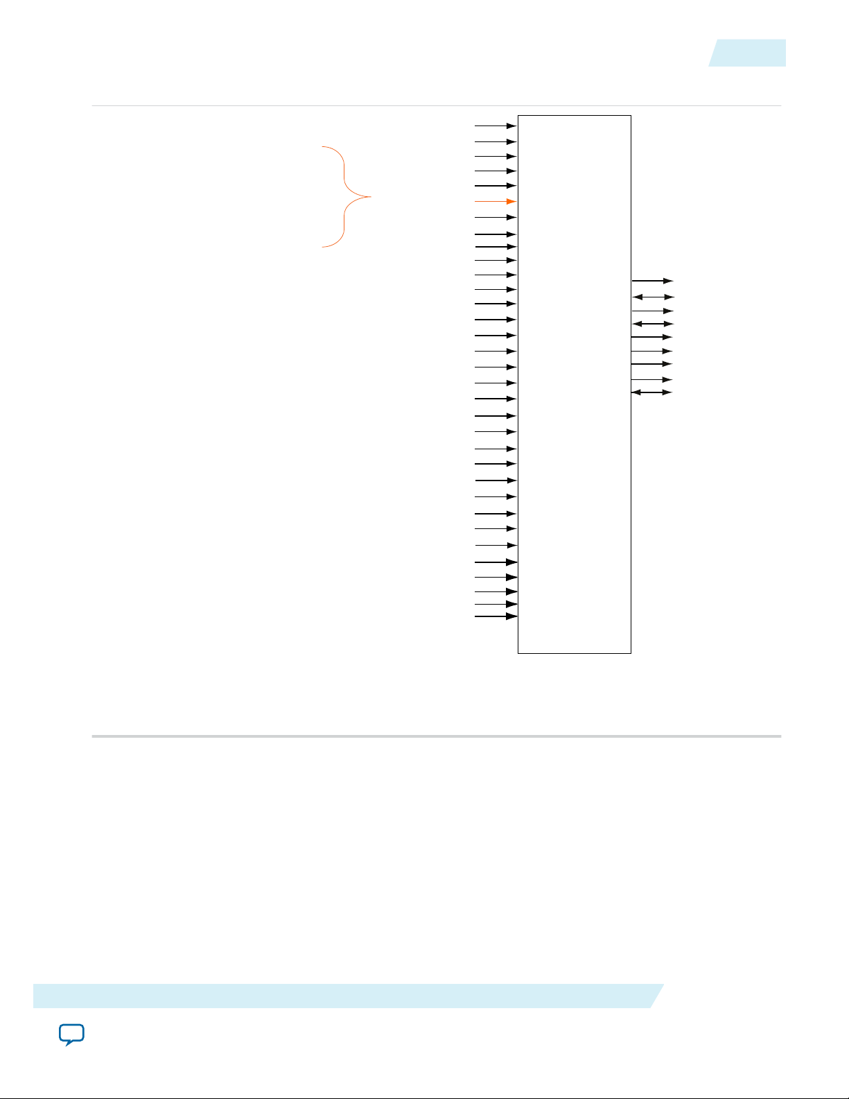
The following figure shows the data strobe, data, termination control, PLL, DLL, hard FIFO, and dynamic
configuration ports of the IP core.
ALTDQ_DQS2 IP Core User Guide
Send Feedback
Page 25
-
ALTDQ_DQS2
config_clock_in
config_data_in
config_dqs_ena
config_dqs_io_ena
config_update
core_clock_in
fr_clock_in
hr_clock_in
lfifo_rden
reset_n_core_clock_in
rfifo_reset_n
strobe_ena_hr_clock_in
vfifo_reset_n
write_strobe_clock_in
dll_delayctrl_in[]
capture_strobe_ena[]
output_strobe_ena[]
oct_ena_in[]
parallelterminationcontrol_in[]
seriesterminationcontrol_in[]
write_oe_in[]
output_strobe_n_out
output_strobe_out
extra_write_data_out[]
write_data_out[]
strobe_n_io
capture_strobe_out
read_data_out[]
strobe_io
read_write_data_io[]
write_data_in[]
config_io_ena[]
lfifo_rdata_en_full[]
lfifo_rd_latency[]
vfifo_qvld[]
vfifo_inc_wr_ptr[]
capture_strobe_n_in
extra_write_data_in[]
read_data_in[]
config_extra_io_ena[]
lfifo_reset_n
capture_strobe_in
This signal is used for QDRII. This clock, unlike
other clocks, can be held at zero during initialization,
which is a requirement for QDRII. Use the core
clock signal for internal purposes. In a half-rate
application, the core clock signal is unconnected. In
a full-rate application, you must connect the core
clock signal to the full-rate clock.
UG-01089
2014.12.17
Figure 15: ALTDQ_DQS2 Block Diagram by Port Types
ALTDQ_DQS2 Ports
25
ALTDQ_DQS2 IP Core User Guide
Altera Corporation
Send Feedback
Page 26

26
ALTDQ_DQS2 Data Strobe Ports
ALTDQ_DQS2 Data Strobe Ports
Table 6: ALTDQ_DQS2 Data Strobe Ports
Port Name Type Width Description
UG-01089
2014.12.17
capture_strobe_ena
capture_strobe_n_in
Input 1 Controls the DQS enable control
block by acting as the gating
signal for signals coming from
the input registers (capture_
strobe_in) to reach the DQS
delay chain block.
This port is only supported in
Stratix V devices.
Input 1 Receives the negative polarity
clock signal from the external
device. For example, a DQSn
signal from the external
memory. This port is available
when the capture strobe type is
set to differential or complemen‐
tary.
This port is supported in Arria
V, Cyclone V, and Stratix V
devices.
capture_strobe_in
capture_strobe_out
Input 1 Receives the clock signal from
the external device, for example,
a DQS signal from the external
memory.
This port is supported in Arria
V, Cyclone V, and Stratix V
devices.
Output 1 Sends the delayed clock signal to
the core. For example, a delayed
DQS signal from the DQS delay
chain.
This port is supported in Arria
V, Cyclone V, and Stratix V
devices.
Altera Corporation
ALTDQ_DQS2 IP Core User Guide
Send Feedback
Page 27

UG-01089
2014.12.17
ALTDQ_DQS2 Data Strobe Ports
Port Name Type Width Description
27
output_strobe_ena
oct_ena_in
reset_n_core_clock_in
write_strobe_clock_in
Input 2 = half-rate
1 = full-rate
The gating signal for the
output_strobe_out port.
This port is supported in Arria
V, Cyclone V, and Stratix V
devices.
Input 2 = half-rate
1 = full-rate
Controls the dynamic on-chiptermination signal for all data
and strobe ports.
This port is supported in Arria
V, Cyclone V, and Stratix V
devices.
Input 1 Asynchronous reset used in
QDRII-like interfaces to reset the
write strobe.
This port is supported in Arria
V, Cyclone V, and Stratix V
devices.
Input 1 Receives the clock signal from
the core. For example, a DQS
signal from the core. Clocks the
DDIO that generates the output
strobe signal.
ALTDQ_DQS2 IP Core User Guide
This port is supported in Arria
V, Cyclone V, and Stratix V
devices.
Note: This signal is the
main full-rate input
clock when you set
the IP type to Input
for Arria V and
Cyclone V devices.
Altera Corporation
Send Feedback
Page 28
28
ALTDQ_DQS2 Data Strobe Ports
Port Name Type Width Description
UG-01089
2014.12.17
strobe_ena_hr_clock_in
strobe_io
strobe_n_io
Input 1 Receives the clock signal from
the clock pin or the PLL to clock
the DQS enable control block.
Also a half-rate signal that, after
going through the DQS_ENABLE_
CTRL input, controls the gating of
the input strobe.
This port is supported in Arria
V, Cyclone V, and Stratix V
devices.
Bidirectional 1 Sends and receives the bidirec‐
tional clock signal.
This port is supported in Arria
V, Cyclone V, and Stratix V
devices.
Bidirectional 1 Sends and receives the negative
polarity clock signal for differen‐
tial or complementary strobe
configuration.
output_strobe_out
output_strobe_n_out
This port is supported in Arria
V, Cyclone V, and Stratix V
devices.
Output 1 Sends clock signal to the external
device. For example, a DQS
signal to the external memory.
This port is supported in Arria
V, Cyclone V, and Stratix V
devices.
Output 1 Sends the negative polarity clock
signal to the external device (For
example, DQSn signal to the
external memory). This port is
available when you set the
output strobe type to differential
or complementary.
This port is supported in Arria
V, Cyclone V, and Stratix V
devices.
Altera Corporation
ALTDQ_DQS2 IP Core User Guide
Send Feedback
Page 29

UG-01089
2014.12.17
ALTDQ_DQS2 Data Ports
The following table lists the ALTDQ_DQS2 data ports where n= number of DQ pins, m= number of
additional output-only DQ pins, x = 0 to (n-1), and y= 0 to (m-1).
Table 7: ALTDQ_DQS2 Data Ports
ALTDQ_DQS2 Data Ports
29
Port Name Type Width
extra_write_data_in[]
extra_write_data_out[]
Description
(2)
Input 2m = full-rate
4m = half-rate
Receives data signal from the
core.
This port connects to the input
port of the half-rate data to
single-rate data output registers
block (Figure 13). In full-rate
mode, only the extra_write_
data_in[y] and extra_write_
data_in[m+y] ports are used.
This port is supported in Arria
V, Cyclone V, and Stratix V
devices.
Output m Sends data to the external device.
This port connects to the output
port of the output buffer (Figure
13).
read_data_in[]
(2)
The port width applies to full-rate mode, unless otherwise specified.
ALTDQ_DQS2 IP Core User Guide
This port is supported in Arria
V, Cyclone V, and Stratix V
devices.
Input n Receives data from the external
device.
This port connects to the input
port of the input buffer located
between the DQ pin and the
DDR input registers block. This
is an input-only DQ port that
receives data from the external
device (Figure 8).
This port is supported in Arria
V, Cyclone V, and Stratix V
devices.
Altera Corporation
Send Feedback
Page 30

30
ALTDQ_DQS2 Data Ports
UG-01089
2014.12.17
Port Name Type Width
read_data_out[]
read_write_data_io[]
(2)
Output 2n = full-rate
4n = half-rate
Bidirec‐
n Receives and sends data between
tional
Description
Sends the captured data from the
external device to the core.
This port connects to the output
port of the DDR input register
block (Figure 8). The read_
data_out[x] port outputs the
positive-edge triggered data, and
the read_data_out[n+x] port
outputs the negative-edge
triggered data.
This port is supported in Arria
V, Cyclone V, and Stratix V
devices.
the core and the external device.
You must assign the bidirec‐
tional DQ port with the output
termination and input termina‐
tion assignments.
write_data_in[]
Input 2n = full-rate
4n = half-rate
This port is supported in Arria
V, Cyclone V, and Stratix V
devices.
Receives DDR data signal from
the core to be sent out to the
external device. For example,
data to be written to the external
memory during write operation.
This port connects to the input
port of the half-rate data to
single-rate data output registers
block (Figure 12). In full-rate
mode, the IP core uses only the
write_data_in[x] and write_
data_in[n+x] ports.
This port is supported in Arria
V, Cyclone V, and Stratix V
devices.
(2)
The port width applies to full-rate mode, unless otherwise specified.
Altera Corporation
ALTDQ_DQS2 IP Core User Guide
Send Feedback
Page 31

UG-01089
2014.12.17
ALTDQ_DQS2 Data Ports
31
Port Name Type Width
write_data_out[]
write_oe_in[]
Description
(2)
Output n Sends the DDR data signal to the
external device. For example,
data to be written to the external
memory during write operation.
This port connects to the output
port of the output buffer located
between the DDR output
registers block and the DQ-out
pin (Figure 12).
This port is supported in Arria
V, Cyclone V, and Stratix V
devices.
Input n = full-rate
2n = half-rate
Receives the gating signal from
the core to control the output
buffer. For example, gating
control when writing data to the
external memory during write
operation.
This port connects to the input
port of the half-rate data to
single-rate data output-enable
registers block (Figure 12). In
full-rate mode, the IP core uses
only the write_oe_in[x] port.
This port is supported in Arria
V, Cyclone V, and Stratix V
devices.
Note: To understand how these ports connect to the IOEs, refer to “I/O Elements” in the External
Memory Interfaces in Stratix V Devices chapter of the Stratix V Device Handbook.
(2)
The port width applies to full-rate mode, unless otherwise specified.
ALTDQ_DQS2 IP Core User Guide
Send Feedback
Altera Corporation
Page 32

32
ALTDQ_DQS2 Termination Control Ports
ALTDQ_DQS2 Termination Control Ports
Table 8: ALTDQ_DQS2 Termination Control Ports
Port name Type Width Description
UG-01089
2014.12.17
parallelterminationcontrol_in[]
seriesterminationcontrol_in[]
Input 16 Controls the calibrated
parallel termination ports
of the input buffers.
You must connect this port
to the paralleltermina-
tioncontrol[15:0] port
of the ALTOCT IP core.
Ensure that the termination
block located in the
ALTOCT instance is
assigned with the termina‐
tion control block
assignment.
This port is supported in
Arria V, Cyclone V, and
Stratix V devices.
Input 16 Controls the calibrated
series termination ports of
the output buffers.
You must connect this port
to the seriestermina-
tioncontrol[15:0] port
of the ALTOCT IP core.
Ensure that the termination
block located in the
ALTOCT instance is
assigned with the termina‐
tion control block
assignment.
Related Information
• DC and Switching Characteristics for Stratix V Devices
Altera Corporation
This port is supported in
Arria V, Cyclone V, and
Stratix V devices.
Describes the dynamic OCT control in Stratix V devices.
ALTDQ_DQS2 IP Core User Guide
Send Feedback
Page 33

UG-01089
2014.12.17
ALTDQ_DQS2 PLL and DLL Ports
Table 9: ALTDQ_DQS2 PLL and DLL Ports
Port name Type Width Description
ALTDQ_DQS2 PLL and DLL Ports
33
dll_delayctrl_in[]
fr_clock_in
hr_clock_in
Input 7 Receives the 7-bit delay settings
from the dll_delayctrlout port of
the ALTDLL instance. This 7-bit
signal controls delay through the
DQS delay chains. Compilation
error occurs if this port is not
connected to a DLL.
This port is supported in Arria V,
Cyclone V, and Stratix V devices.
Input 1 Receives the full-rate clock signal
from a clock pin, or the PLL clock
output port.
This port is supported in Arria V,
Cyclone V, and Stratix V devices.
Input 1 Receives the half-rate clock signal
from a clock pin, or the PLL clock
output port.
This port is supported in Arria V,
Cyclone V, and Stratix V devices.
Note: For more information about DLL in Stratix V device, refer to “Delay-Locked Loop” in the External
Memory Interfaces in Stratix V Devices chapter of the Stratix V Device Handbook.
Note: For more information about PLL in Stratix V devices, refer to “PLL Specifications” in DC and
Switching Characteristics for Stratix V Devices chapter of the Stratix V Device Handbook.
ALTDQ_DQS2 IP Core User Guide
Send Feedback
Altera Corporation
Page 34

34
ALTDQ_DQS2 Hard FIFO Ports
ALTDQ_DQS2 Hard FIFO Ports
Table 10: Hard FIFO Ports
Ports Type Width Description
UG-01089
2014.12.17
lfifo_rdata_en_full
lfifo_rden Input
Input 2 Data input to the latency shifter
FIFO. This signal is the full read
enable token generated by user
logic and is asserted for the
length of the desired read burst.
This token is delayed by a
variable number of integer cycles
inside the latency shifter FIFO
and used to feed the read enable
signal of the read FIFO.
This port is only supported in
Arria V and Cyclone V devices.
1 Data input to the Read FIFO
Read Enable. This signal is the
full read enable token generated
by user logic and is asserted for
the length of the desired read
burst.
This port is only supported in
Stratix V devices.
lfifo_reset_n
lfifo_rd_latency[]
Altera Corporation
Input 1 Active high reset to the latency
shifter FIFO
This port is only supported in
Arria V and Cyclone V devices.
Input 5 The number of cycles to delay
data inputs feeding the latency
shifter FIFO. A maximum of 31
cycles is supported.
This port is only supported in
Arria V and Cyclone V devices.
ALTDQ_DQS2 IP Core User Guide
Send Feedback
Page 35

UG-01089
2014.12.17
ALTDQ_DQS2 Dynamic Configuration Ports
Ports Type Width Description
35
vfifo_qvld
vfifo_inc_wr_ptr
vfifo_reset_n
Input Arria V and
Cyclone V
devices: 2
Stratix V
devices: 1
Data input to the data valid
FIFO. This signal is the full read
enable token generated by user
logic and is asserted for the
length of the desired read burst.
This signal is driven by the same
user logic that drives the lfifo_
rdata_en_full signal.
In general applications, you can
leave this port unconnected.
This port is supported in Arria
V, Cyclone V, and Stratix V
devices.
Input 2 Increments the latency
implemented by the data valid
FIFO by one cycle.
This port is only supported in
Arria V and Cyclone V devices.
Input 1 Active high reset to the data
valid FIFO
rfifo_reset_n
Input 1 Active high reset to the read
The I/O and DQS configuration blocks represent a set of serial-to-parallel shift registers that dynamically
changes the settings of various device configuration bits. The I/O and DQS configuration blocks shift a
serial configuration data stream into the shift registers, and then load the data stream into the configura‐
tion registers. The shift registers power-up low. Every I/O pin contains an I/O configuration block. Every
DQS group contains a DQS configuration block and an I/O configuration block.
ALTDQ_DQS2 Dynamic Configuration Ports
The following table lists the dynamic configuration ports where n= number of DQ pins and m= number
of additional DQ pins.
This port is only supported in
Arria V and Cyclone V devices.
FIFO .
This port is only supported in
Arria V and Cyclone V devices.
ALTDQ_DQS2 IP Core User Guide
Send Feedback
Altera Corporation
Page 36

36
ALTDQ_DQS2 Dynamic Configuration Ports
Table 11: ALTDQ_DQS2 Dynamic Configuration Ports
Port name Type Width Description
UG-01089
2014.12.17
config_clock_in
config_data
Input 1 The ALTDQ_DQS2 dynamic
configuration interface consists
of this input port.
Receives the clock signal to
clock all dynamic configuration
blocks. You can connect this
port to a clock pin, or the PLL
clock output port.
This is the clock signal. All other
input signals must be treated as
synchronous to this clock.
This port is supported in Arria
V, Cyclone V, and Stratix V
devices.
Input 1 The ALTDQ_DQS2 dynamic
configuration interface consists
of this input port.
The 1-bit serial input through
which data is scanned into the
calibration blocks. It is common
to all configuration blocks, but it
will only be scanned into
calibrations blocks whose enable
input is asserted.
config_io_ena[]
Altera Corporation
This port is supported in Arria
V, Cyclone V, and Stratix V
devices.
Input n An input port that controls the
enable input on the DQ I/O
configurations. Receives the
clock enable signal for the I/O
configuration block.
Refer to Dynamic Reconfigura‐
tion for ALTDQ_DQS2 on
page 38
This port is supported in Arria
V, Cyclone V, and Stratix V
devices.
ALTDQ_DQS2 IP Core User Guide
Send Feedback
Page 37

UG-01089
2014.12.17
ALTDQ_DQS2 Dynamic Configuration Ports
Port name Type Width Description
37
config_dqs_io_ena
config_dqs_ena
Input 1 An input port that controls the
enable input on the DQS I/O
configurations. Receives the
clock enable signal for the DQS
I/O configuration block.
Refer to Dynamic Reconfigura‐
tion for ALTDQ_DQS2 on
page 38
This port is supported in Arria
V, Cyclone V, and Stratix V
devices.
Input 1 An input port that controls the
enable input on the DQS logic.
Receives the clock enable signal
for the DQS configuration
block.
Refer to Dynamic Reconfigura‐
tion for ALTDQ_DQS2 on
page 38
config_update
This port is supported in Arria
V, Cyclone V, and Stratix V
devices.
Input 1 The ALTDQ_DQS2 dynamic
configuration interface consists
of this input port.
Receives the signal to load the
bits from the serial-to-parallel
shift registers to the configura‐
tion registers.
After scanning all the bits into
the desired scan chain blocks,
the bits can be copied at once
into the configuration register
by asserting the config_update
signal for one clock cycle.
This port is supported in Arria
V, Cyclone V, and Stratix V
devices.
ALTDQ_DQS2 IP Core User Guide
Send Feedback
Altera Corporation
Page 38

38
Dynamic Reconfiguration for ALTDQ_DQS2
Port name Type Width Description
UG-01089
2014.12.17
config_data_in
config_extra_io_ena[]
Input 1 Receives the serial configuration
Input m Receives the clock enable signal
Note: For more information about the dynamic configuration blocks in Stratix V device, refer to “I/O
Configuration Block and DQS Configuration Block” in the External Memory Interfaces in Stratix
V Devices chapter of the Stratix V Device Handbook.
Dynamic Reconfiguration for ALTDQ_DQS2
data stream that shifts into the
serial-to-parallel shift registers.
This port is supported in Arria
V, Cyclone V, and Stratix V
devices.
for the additional I/O configura‐
tion block.
This port is supported in Arria
V, Cyclone V, and Stratix V
devices.
When static timing closure is challenging (for example, high frequency, high board trace skew, and high
timing uncertainty), dynamically reconfiguring the ALTDQ_DQS2 IP core may provide additional timing
margin. Arria V, Cyclone V, and Stratix V devices contain reconfigurable logic, allowing you to adjust the
delay of several datapaths at runtime.
The I/O configuration block and the DQS configuration block are shift registers that you can use to
dynamically change the settings of various device configuration bits. The shift registers are configured
with the rest of the device when the Programmer Object File (.pof). In dynamic mode, you can override
the static values at runtime with a scan chain. You can reconfigure the I/Os by turning on the Use
dynamic configuration scan chains option.
The following figure shows the Use dynamic configuration scan chains option.
Figure 16: Use Dynamic Configuration Scan Chains Option
The following figure shows the dynamic reconfiguration scan chain implementation.
Altera Corporation
ALTDQ_DQS2 IP Core User Guide
Send Feedback
Page 39

din
update
enable
clk
DQ0
din
update
enable
clk
DQ1
din
update
enable
clk
DQS
config_data
config_update
config_clock_in
config_io_ena[0] config_io_ena[1] config_dqs_ena
UG-01089
2014.12.17
Dynamic Reconfiguration for ALTDQ_DQS2
Figure 17: Reconfiguration Scan Chain
Each I/O contains a scan chain block. The DQS logic also contains its own scan chain block. You can use
I/O scan chain blocks to configure DQ and DQS I/O configuration registers (for example, delay chain)
and you can use the DQS logic scan chain to configure DQS logic configuration (for example, DQS
postamble phase). You can serially scan configuration bits into each scan chain block with the following
operating sequence:
39
The ALTDQ_DQS2 dynamic configuration interface is made of four input ports:
• config_clock_in—This is the clock signal. All other input signals must be treated as synchronous to
this clock. The typical frequency is 25 MHz.
• config_data—This is the 1-bit serial input through which data is scanned into the calibration blocks.
This is common to all configuration blocks, but it will only be scanned into calibrations blocks whose
enable input is asserted. Configuration data must be input in LSB first ordering. For example, the
Stratix V I/O configuration block data must start with padtoinputregisterdelaysetting[0].
• config_enable—In a generic ALTDQ_DQS2 IP core, the following three config_enable inputs are
available:
• config_io_ena[]—Controls the enable input on the DQ I/Os
• config_dqs_io_ena[]—Controls the enable input on the DQS I/Os
• config_dqs_ena[]—Controls the enable input on the DQS logic
Note:
Each of these inputs is wide to control all the scan chain blocks instantiated in the
ALTDQ_DQS2 IP core. In a general application, you must assert only one enable input at a
time to scan the desired data in the corresponding scan chain block. The enable input must be
held high for the entire duration of the scanning process. All other inputs must be held at 0.
Note: You must deassert the config_enable signal after the last bit of config_data to prevent
further data from scanning in. Then, assert the update signal whenever you are ready to copy
the scanned in data to the configuration registers.
• config_update—After scanning all the bits into the desired scan chain blocks, copy them into the
configuration register by asserting the config_update signal for one clock cycle.
ALTDQ_DQS2 IP Core User Guide
Send Feedback
Altera Corporation
Page 40

1
0
DQ
D1
Delay
Chain
D1
Delay
Chain
AB
Positive Edge
Read Data
Negative Edge
Read Data
D4
Delay
Chain
D4
Delay
Chain
EF
DQS
Delay
Chain
T
DQS
T11
Delay
Chain
T11
Delay
Chain
R
To dqsenable
Port
To dqsdisablen
Port
DQS
Enable
Control
Q
S
From
dqsenableout
Port
Clock Phase
Select
Clock Phase
Select (0 Degree)
To
levelingclk
Port
To
zerophaseclk
Port
M N
X V
Output
Alignment
Clock Phase
Select (0 Degree)
Output
Alignment
W U
Output
Alignment
Output
Alignment
Negative Edge
Write Data
Positive Edge
Write Data
W U
Output
Alignment
1
0
Negative Edge
Write Data
Positive Edge
Write Data
X V
Output
Alignment
Output Enable
Signal
Clock Phase
Select
Clock Phase
Select (0 Degree)
I J
Leveling
Delay
Chain
Clock Signal
from Core
Clock Phase
Select
K L
Output Enable
Signal
O P
Output
Alignment
OCT Control
Signal
DQ
D5
Delay
Chain
D5
Delay
Chain
D6 OCT
Delay
Chain
D6 OE
Delay
Chain
D5 OCT
Delay
Chain
D5 OE
Delay
Chain
DQS
D5
Delay
Chain
D5
Delay
Chain
D5 OCT
Delay
Chain
D5 OE
Delay
Chain
D6 OCT
Delay
Chain
D6 OE
Delay
Chain
C
D
G
H
D2
Delay
Chain
D3
Delay
Chain
-
D6
Delay
Chain
D6
Delay
Chain
D5 OCT
Delay
Chain
D5 OE
Delay
Chain
D5 OCT
Delay
Chain
D5 OE
Delay
Chain
Use the combination of D1, D2, D3, and D4 delay chains for calibration. Use D1, D2, and D3 to delay
DQ, and D4 delay chain to delay DQS. D5 and D6 delay chains are the output delay chains.
The D2 and D3 delay chains are static input delay chains. The D6 delay chain is static output delay
chain. You can only set the settings in the Q uartus II Settings File (.qsf) or the Fitter sets the settings
automatically based on the timing constraints. You cannot dynamically set the settings.
40
I/O Configuration Block Bit Sequence for Arria V GZ and Stratix V Devices
I/O Configuration Block Bit Sequence for Arria V GZ and Stratix V Devices
Figure 18: I/O and DQS Delay Chains for Arria V GZ and Stratix V Devices
UG-01089
2014.12.17
The following tables lists the I/O configuration block bit sequence, description, and settings for Arria V
GZ and Stratix V devices.
Table 12: I/O Configuration Block Bit Sequence for Arria V GZ and Stratix V Devices
Bit
Legend
in
Figure
18
A 5..0 padtoinputregisterdelaysetting Connects to the delayctrlin port of
Altera Corporation
Bit Name Description
the D1 delay chain to control the first I/
O buffer-to-input register delay chain
(D1).
Sets to tune the DQ delay (read calibra‐
tion) for DDR applications.
For delay values, refer to the “Program‐
mable IOE Delay” section in the Stratix
V Device Datasheet.
ALTDQ_DQS2 IP Core User Guide
Send Feedback
Page 41

UG-01089
2014.12.17
I/O Configuration Block Bit Sequence for Arria V GZ and Stratix V Devices
41
Legend
in
Figure
18
Bit
Bit Name Description
B 11..6 padtoinputregisterrisefalldelaysetting Connects to the delayctrlin port of
the second D1 delay chain to control the
second pad-to-input register delay chain
(D1).
For delay values, refer to the “Program‐
mable IOE Delay” section in the Stratix
V Device Datasheet.
C 17..12 outputdelaysetting1 Connects to the delayctrlin port of
the D5 delay chain to control the output
register-to-I/O buffer delay chain (D5)
in the output path and output enable
paths.
This delay is for write calibration for
DDR application.
For delay values, refer to the “Program‐
mable IOE Delay” section in the Stratix
V Device Datasheet.
D 23..18 outputdelaysetting2 Connects to the delayctrlin port of
the second D5 delay chain to control the
output register-to-I/O buffer delay chain
(second D5) in the output path and
output enable paths.
This delay is for write calibration for
DDR application.
For delay values, refer to the “Program‐
mable IOE Delay” section in the Stratix
V Device Datasheet.
— 39..24 inputclkndelaysetting
inputclkdelaysetting
Unconfigurable bits.
Always set bits to its default value.
dutycycledelaymode
dutycycledelaysetting
ALTDQ_DQS2 IP Core User Guide
Send Feedback
Altera Corporation
Page 42

42
DQS Configuration Block Bit Sequence for Arria V GZ and Stratix V Devices
Table 13: I/O Configuration Block Bit Value for Arria V GZ and Stratix V Devices
UG-01089
2014.12.17
Bit
Bit Name/
Bit
Default Value
(Binary)
Min.
Value
5..0 padtoinputregisterdelaysetting 000000 intrin
sic
delay
11..6 padtoinputregisterrisefalldelayset‐
ting
000000 intrin
sic
delay
17..12 outputdelaysetting1 000000 intrin
sic
delay
23..18 outputdelaysetting2 000000 intrin
sic
delay
39..24 inputclkndelaysetting
inputclkdelaysetting
0000000000000
000
— — —
dutycycledelaymode
Max.
Value
787.5 ps +
intrinsic
delay
787.5 ps +
intrinsic
delay
787.5 ps +
intrinsic
delay
787.5 ps +
intrinsic
delay
Inc. Value
12.5 ps
12.5 ps
12.5 ps
12.5 ps
dutycycledelaysetting
Related Information
Stratix V Device Datasheet
DQS Configuration Block Bit Sequence for Arria V GZ and Stratix V Devices
The following tables lists the DQS configuration block bit sequence, description, and settings for Arria V
GZ and Stratix V devices.
Altera Corporation
ALTDQ_DQS2 IP Core User Guide
Send Feedback
Page 43

UG-01089
2014.12.17
DQS Configuration Block Bit Sequence for Arria V GZ and Stratix V Devices
Table 14: DQS Configuration Block Bit Sequence for Arria V GZ and Stratix V Devices
43
Legend in I/O Configu‐
ration Block Bit
Sequence for Arria V
GZ and Stratix V
Devices on page 40
Bit Bit Name Description
E 5..0 dqsbusoutdelaysetting Connects to the delayctrlin port
of the first D4 delay chain.
Controls the first D4 delay chain
in DQS delay chain path (after
the DQS delay chain). This is the
delay tuning of the DQS signal
feeding into the DQS bus.
For delay values, refer to the
“Programmable IOE Delay”
section in the Stratix V Device
Datasheet.
F 11..6 dqsbusoutdelaysetting2 Connects to the delayctrlin port
of the second D4 delay chain.
Controls the second D4 delay
chain in DQS delay chain path
(after the first D4 delay chain).
This is the delay tuning of the
DQS signal feeding into the DQS
bus.
For delay values, refer to the
“Programmable IOE Delay”
section in the Stratix V Device
Datasheet.
G 17..12 octdelaysetting1 Connects to the delayctrlin port
of the D5 OCT delay chain.
Controls the dynamic OCT
output register-to-I/O buffer
delay chain (D5).
For delay values, refer to the
“Programmable IOE Delay”
section in the Stratix V Device
Datasheet.
ALTDQ_DQS2 IP Core User Guide
Send Feedback
Altera Corporation
Page 44

44
DQS Configuration Block Bit Sequence for Arria V GZ and Stratix V Devices
UG-01089
2014.12.17
Legend in I/O Configu‐
ration Block Bit
Sequence for Arria V
GZ and Stratix V
Devices on page 40
Bit Bit Name Description
H 23..18 octdelaysetting2 Connects to the delayctrlin
port of the second D5 OCT delay
chain.
Controls the dynamic OCT
output register-to-I/O buffer
delay chain (second D5).
For delay values, refer to the
“Programmable IOE Delay”
section in the Stratix V Device
Datasheet.
— 27..24 addrphasesetting
addrpowerdown
addrphaseinvert
Unconfigurable bits.
Always set bits to its default
value.
I 29..28 dqsoutputphasesetting Connects to the phasectrlin port
of the clock phase select (in the
DQS output path) to select
between phase shifts of 0°, 45°,
90°, and 135°.
Use this bit to level the DQS
write output.
— 30 dqsoutputpowerdown Unconfigurable bits.
Always set bits to its default
value.
J 31 dqsoutputphaseinvert Connects to the phaseinvertctrl
port of the clock phase select (in
the DQS output path) to select
between the non-inverted and
inverted output.
This setting allows the phase
output from the delay chain to be
inverted to gain additional
phases.
Altera Corporation
ALTDQ_DQS2 IP Core User Guide
Send Feedback
Page 45

UG-01089
2014.12.17
DQS Configuration Block Bit Sequence for Arria V GZ and Stratix V Devices
45
Legend in I/O Configu‐
ration Block Bit
Sequence for Arria V
GZ and Stratix V
Devices on page 40
Bit Bit Name Description
K 33..32 dqoutputphasesetting Connects to the phasectrlin port
of the clock phase select (in the
DQ output path) to select
between phase shifts of 0°, 45°,
90°, and 135°.
DQ leveling clock select. n Use
this bit to level the DQ write
output.
— 35..34 dqoutputpowerdown Unconfigurable bits.
Always set bits to its default
value.
L 36 dqoutputphaseinvert Connects to the phaseinvertctrl
port of the clock phase select (in
the DQ output path) to select
between the non-inverted and
inverted output.
This setting allows the phase
output from the delay chain to be
inverted to gain additional
phases.
— 40..37 resyncinputphasesetting
resyncinputpowerdown
resyncinputphaseinvert
Unconfigurable bits.
Always set bits to its default
value.
M 42..41 postamblephasesetting Connects to the phasectrlin port
of the clock phase select (for the
DQS enable control block) to
select between phase shifts of 0°,
45°, 90°, and 135°.
Use this clock phase select block
to level the postamble
(dqsenablein signal at the DQS
enable control block).
— 44..43 postamblepowerdown Unconfigurable bits.
Always set bits to its default
value.
ALTDQ_DQS2 IP Core User Guide
Send Feedback
Altera Corporation
Page 46

46
DQS Configuration Block Bit Sequence for Arria V GZ and Stratix V Devices
UG-01089
2014.12.17
Legend in I/O Configu‐
ration Block Bit
Sequence for Arria V
GZ and Stratix V
Devices on page 40
Bit Bit Name Description
N 45 postamblephaseinvert Connects to the phaseinvertctrl
port of the clock phase select (for
the DQS enable control block) to
select between the non-inverted
and inverted output.
Use this clock phase select block
to level the postamble
(dqsenablein signal at the DQS
enable control block).
This setting allows the phase
output from the delay chain to be
inverted to gain additional
phases.
— 65..46 dqs2xoutputphasesetting
n dqs2xoutputpowerdown
dqs2xoutputphaseinvert
Unconfigurable bits.
Always set bits to its default
value.
dq2xoutputphasesetting
dq2xoutputpowerdown
dq2xoutputphaseinvert
ck2xoutputphasesetting
ck2xoutputpowerdown
ck2xoutputphaseinvert
dqoutputzerophasesetting
postamblezerophasesetting
postamblepowerdown
dividerioehratephaseinvert
dividerphaseinvert
O 68..66 enaoctcycledelaysetting Connects to the enaoutputcycle‐
delay port of the output
alignment block (in the dynamic
OCT control path) to allow
additional registers to be used.
Use this bit to adjust the phase of
the write-leveled OCT or output
data signal.
Altera Corporation
ALTDQ_DQS2 IP Core User Guide
Send Feedback
Page 47

UG-01089
2014.12.17
DQS Configuration Block Bit Sequence for Arria V GZ and Stratix V Devices
47
Legend in I/O Configu‐
ration Block Bit
Sequence for Arria V
GZ and Stratix V
Devices on page 40
Bit Bit Name Description
P 69 enaoctphasetransferreg Connects to the enaphasetrans‐
ferreg port of the output
alignment block (in the dynamic
OCT control path) to allow an
additional negative edgetriggered register to be added to
the OCT, output data, or output
enable path to satisfy the setup or
hold time requirement for the
phase transfer.
Q 77..70 dqsdisablendelaysetting Connects to the delayctrlin port
of the T11 delay chain (located
between the dqsenableout port of
the DQS enable control block
and the dqsdisablen port of the
DQS delay chain).
This is to align post-amble signal
in terms of DQS signal by
selecting different delays.
R 85..78 dqsenabledelaysetting Connects to the delayctrlin port
of the T11 delay chain (located
between the dqsenableout port of
the DQS enable control block
and the dqsenable port of the
DQS delay chain).
This is to align post-amble signal
in terms of DQS signal by
selecting different delays.
S 86 enadqsenablephasetransferreg Connects to the enaphasetrans‐
ferreg port of the DQS enable
control block to allow an
additional negative edgetriggered register to be added to
the DQS enable control path to
satisfy the setup or hold time
requirement for the phase
transfer.
ALTDQ_DQS2 IP Core User Guide
Send Feedback
Altera Corporation
Page 48

48
DQS Configuration Block Bit Sequence for Arria V GZ and Stratix V Devices
UG-01089
2014.12.17
Legend in I/O Configu‐
ration Block Bit
Sequence for Arria V
GZ and Stratix V
Devices on page 40
Bit Bit Name Description
T 88..87 dqsinputphasesetting Connects to the phasectrlin port
of the DQS delay chain block.
To control the phase selection for
the DQS delay chain.
The frequency range that this
works at is 300 MHz to 800 MHz.
U 89 enadqsphasetransferreg Connects to the enaphasetrans‐
ferreg port of the output
alignment block (in the DQS
output path and OE path) to
allow an additional negative
edge-triggered register to be
used.
V 90 enaoutputphasetransferreg Connects to the enaphasetrans‐
ferreg port of the output
alignment block (in the DQ
output path and OE path) to
allow an additional negative
edge-triggered register to be
added to the output data or
output enable path to satisfy the
setup or hold time requirement
for the phase transfer.
W 93..91 enadqscycledelaysetting Connects to the enaoutputcycle‐
Altera Corporation
delay port of the output
alignment block (in the DQS
output path and OE path) to
allow additional registers to be
enabled in the output alignment
block of the output data or
output enable path of a DQS I/O.
This is normally used to adjust
the phase of the write-leveled
OCT or output data signal.
ALTDQ_DQS2 IP Core User Guide
Send Feedback
Page 49

UG-01089
2014.12.17
DQS Configuration Block Bit Sequence for Arria V GZ and Stratix V Devices
49
Legend in I/O Configu‐
ration Block Bit
Sequence for Arria V
GZ and Stratix V
Devices on page 40
Bit Bit Name Description
X 96..94 enaoutputcycledelaysetting Connects to the enaoutputcycle‐
delay port of the output
alignment block (in the DQ
output path and OE path) to
allow additional registers to be
enabled in the output alignment
block of the output data or
output enable path of a DQ I/O.
Use this bit to adjust the phase of
the write-leveled OCT or output
data signal.
— 100..97 enainputcycledelaysetting
enainputphasetransferreg
Unconfigurable bits.
Always set bits to its default
value.
Table 15: DQS Configuration Block Bit Value for Arria V GZ and Stratix V Device
Bit Bit Name Default Value (Binary) Min
Value
5..0 dqsbusoutdelaysetting 0 intrin
sic
delay
11..6 dqsbusoutdelaysetting2 0 intrin
sic
delay
17..12 octdelaysetting1 0 intrin
sic
delay
23..18 octdelaysetting2 0 intrin
sic
delay
27..24 addrphasesetting
100 — — —
addrpowerdown
addrphaseinvert
Max Value Inc. Unit
787.5 ps +
12.5 ps
intrinsic
delay
787.5 ps +
12.5 ps
intrinsic
delay
787.5 ps +
12.5 ps
intrinsic
delay
787.5 ps +
12.5 ps
intrinsic
delay
ALTDQ_DQS2 IP Core User Guide
Send Feedback
Altera Corporation
Page 50

50
DQS Configuration Block Bit Sequence for Arria V GZ and Stratix V Devices
UG-01089
2014.12.17
Bit Bit Name Default Value (Binary) Min
Value
Max Value Inc. Unit
29..28 dqsoutputphasesetting 0 00 = 0°
01 = 45°
10 = 90°
11 = 135°
30 dqsoutputpowerdown 1 —
31 dqsoutputphaseinvert 0 0 = bypass
1 = enable
33..32 dqoutputphasesetting 0 00 = 0°
01 = 45°
10 = 90°
11 = 135°
35..34 dqoutputpowerdown 10 —
36 dqoutputphaseinvert 0 0 = bypass
1 = enable
40..37 resyncinputphasesetting
100 —
resyncinputpowerdown
resyncinputphaseinvert
42..41 postamblephasesetting 0 00 = 0°
01 = 45°
10 = 90°
11 = 135°
44..43 postamblepowerdown 10 —
45 postamblephaseinvert 0 0 = bypass
1 = enable
Altera Corporation
ALTDQ_DQS2 IP Core User Guide
Send Feedback
Page 51

UG-01089
2014.12.17
DQS Configuration Block Bit Sequence for Arria V GZ and Stratix V Devices
51
Bit Bit Name Default Value (Binary) Min
65..46 dqs2xoutputphasesetting
dqs2xoutputpowerdown
0010_0000_1000_1000_
0100
dqs2xoutputphaseinvert
dq2xoutputphasesetting
dq2xoutputpowerdown
dq2xoutputphaseinvert
ck2xoutputphasesetting
ck2xoutputpowerdown
ck2xoutputphaseinvert
dqoutputzerophasesetting
postamblezerophasesetting
postamblepowerdown
dividerioehratephaseinvert
dividerphaseinvert
Max Value Inc. Unit
Value
—
68..66 enaoctcycledelaysetting 10 000: Not supported
001: Not supported
010: No delay
011: 1 cycle delay
100: 2 cycle delay
101: 3 cycle delay
110: Not supported
111: Not supported
69 enaoctphasetransferreg 0 0 = bypass
1 = enable
77..70 dqsdisablendelaysetting 0 intrin
sic
delay
85..78 dqsenabledelaysetting 0 intrin
sic
delay
3.2 ns +
intrinsic
delay
3.2 ns +
intrinsic
delay
12.5 ps
12.5 ps
86 enadqsenablephasetrans‐
ferreg
ALTDQ_DQS2 IP Core User Guide
Send Feedback
0 0 = bypass
1 = enable
Altera Corporation
Page 52

52
DQS Configuration Block Bit Sequence for Arria V GZ and Stratix V Devices
UG-01089
2014.12.17
Bit Bit Name Default Value (Binary) Min
Value
Max Value Inc. Unit
88..87 dqsinputphasesetting 0 00 = 0°
01 = 45°
10 = 90°
11 = 135°
89 enadqsphasetransferreg 0 0 = bypass
1 = enable
90 enaoutputphasetransferreg 0 0 = bypass
1 = enable
93..91 enadqscycledelaysetting 10 000: Not supported
001: Not supported
010: No delay
011: 1 cycle delay
100: 2 cycle delay
101: 3 cycle delay
110: Not supported
111: Not supported
96..94 enaoutputcycledelaysetting 10 000: Not supported
001: Not supported
010: No delay
011: 1 cycle delay
100: 2 cycle delay
101: 3 cycle delay
110: Not supported
111: Not supported
100..97 enainputcycledelaysetting
0 —
enainputphasetransferreg
Related Information
• Stratix V Device Datasheet
Altera Corporation
ALTDQ_DQS2 IP Core User Guide
Send Feedback
Page 53

4
Open Drain
Programmable
Pull-Up Resistor
4
PRN
D Q
PRN
D Q
PRN
D Q
PRN
D Q
PRN
D Q
clkout
D5 Delay
PRN
D Q
PRN
D Q
D5_OCT
2
From
Core
OE from
Core
Write Data
from Core
To Core
To Core
Read Data
to Core
Read
FIFO
D3_1
Delay
Half Data
Rate Block
Half Data
Rate Block
DQS Logic Block
Dynamic OCT Control (2)
V
CCIO
D5 Delay
Output Buffer
Input Buffer
Programmable
Current Strength
and Slew Rate Control
From OCT
Calibration
Block
On-Chip
Termination
Bus Hold Circuit
D3_0
Delay
D1
Delay
Output Register
Output Register
OE Register
OE Register
Input Register
Input Register Input Register
DQ
DQS
Delay
Chain
D4
Delay
Chain
Leveling
Delay
Chain
I
K
G
H
N
M
L
D
Mode
rdclk
A
C
F
B
J
E
Read FIFO
Clock Select
DQS
T11
Gating
Delay
Chain
T11
Ungating
Delay
Chain
DQS
Enable
Control
Latency
Shifter FIFO
Data Valid
FIFO
Clock
Phase
Select
Clock Signal
from Core
Clock Select
UG-01089
2014.12.17
I/O Configuration Block Bit Sequence for Arria V and Cyclone V Devices
I/O Configuration Block Bit Sequence for Arria V and Cyclone V Devices
Figure 19: I/O and DQS Delay Chains for Arria V and Cyclone V Devices
53
The following table lists the I/O configuration block bit sequence, description, and settings for Arria V
and Cyclone V devices.
ALTDQ_DQS2 IP Core User Guide
Send Feedback
Altera Corporation
Page 54

54
I/O Configuration Block Bit Sequence for Arria V and Cyclone V Devices
Table 16: I/O Configuration Block Bit Sequence for Arria V and Cyclone V Devices
Legend in Figure 19 Bit External Bit Name Description
A 4..0 padtoinputregisterdelaysetting Connects to the delayctrlin
port of the D1 delay chain.
Controls the I/O buffer-to-
input register delay chain
(D1).
Tunes the DQ delay (read
calibration) for DDR
applications.
For delay values, refer to the
“Programmable IOE Delay”
sections in the Arria V
Device Datasheet and the
Cyclone V Device
Datasheet, respectively.
B 9..5 outputenabledelaysetting Connects to the delayctrlin
port of the D5 delay chain.
UG-01089
2014.12.17
Controls the output registerto-I/O buffer delay chain
(D5) in the output enable
paths. This delay is used for
write calibration for DDR
application.
For delay values, refer to the
“Programmable IOE Delay”
sections in the Arria V
Device Datasheet and the
Cyclone V Device
Datasheet, respectively.
C 14..10 outputregdelaysetting Connects to the delayctrlin
port of the D5 delay chain.
Controls the output register-
to-IO Buffer delay chain
(D5) in the output path
paths. This delay is used for
write calibration for DDR
application.
For delay values, refer to the
“Programmable IOE Delay”
sections in the Arria V
Device Datasheet and the
Cyclone V Device
Datasheet, respectively.
Altera Corporation
ALTDQ_DQS2 IP Core User Guide
Send Feedback
Page 55

UG-01089
2014.12.17
I/O Configuration Block Bit Sequence for Arria V and Cyclone V Devices
Legend in Figure 19 Bit External Bit Name Description
D 17..15 readfifomode Connects to the dynfifomode
port of input register read
FIFO block. The read FIFO
can be configured as a read
FIFO or a Unified SerDes
Block.
E 19..18 readfiforeadclockselect Connects to the clksel port of
the read FIFO clock select
block. This controls the read
FIFO Read clock source
Select.
F 20 outputhalfratebypass Sets the multiplexer in the
output enable and output
data path logic to
dynamically bypass the halfrate to full-rate DDIO. Used
only with the hard PHY.
55
— 24..21 Not mapped to any port Unconfigurable bits. Always
set bits to its default value.
Table 17: I/O Configuration Block Bit Sequence for Arria V and Cyclone V Devices
Bit Bit Name Defaul
Value
(Binar
4..0 padtoinputregisterdelayset‐
ting
t
y)
0 intrinsic delay 775 ps + intrinsic
Min. Value Max. Value Inc. Value
delay
9..5 outputenabledelaysetting 0 intrinsic delay 775 ps + intrinsic
delay
14..10 outputregdelaysetting 0 intrinsic delay 775 ps + intrinsic
delay
25 ps
25 ps
25 ps
ALTDQ_DQS2 IP Core User Guide
Send Feedback
Altera Corporation
Page 56

56
DQS Configuration Block Bit Sequence for Arria V and Cyclone V Devices
UG-01089
2014.12.17
Bit Bit Name Defaul
t
Value
(Binar
y)
Min. Value Max. Value Inc. Value
17..15 readfifomode 0 000: Half-rate Read FIFO Mode
001: Full-rate Read FIFO Mode
010: Deserializer Bit Slip Mode
011: Deserializer with Input from Bit Slip
100: Deserializer with Input from I/O
101: Serializer mode
110: Not supported
111: Not supported
19..18
readfiforeadclockselect 0 00: Select Core CLKIN1
01: Select DQS_CLK (PHY_CLK)
10: Select SEQ_HR_CLK (PHY_CLK)
11: Select VCC (Disabled)
20 outputhalfratebypass 0 0: Engage Half-Rate Register
1: Bypass Half-Rate Register
24..21 Not mapped to any port 0 — — —
Related Information
• Arria V Device Datasheet
• Cyclone V Device Datasheet
DQS Configuration Block Bit Sequence for Arria V and Cyclone V Devices
The following tables lists the DQS configuration block bit sequence, description, and settings for Arria V
and Cyclone V devices.
Table 18: DQS Configuration Block Bit Sequence for Arria V and Cyclone V Devices
Legend in Figure 19 Bit Bit Name Description
G 4..0 dqsenableungatingdelaysetting Connects to the delayctrlin port
of postamble T11 delay chain
(ungated). Aligns the postamble
signal in terms of DQS signal by
selecting different delays.
Altera Corporation
ALTDQ_DQS2 IP Core User Guide
Send Feedback
Page 57

UG-01089
2014.12.17
DQS Configuration Block Bit Sequence for Arria V and Cyclone V Devices
Legend in Figure 19 Bit Bit Name Description
H 9..5 dqsenablegatingdelaysetting Connects to the delayctrlin port
of the postamble T11 delay
chain (gated). Aligns the
postamble signal in terms of
DQS signal by selecting
different delays.
I 10 enadqsenablephasetransferreg Connects to the enaphasetrans‐
ferreg port of the DQS Enable
Control block to allow an
additional negative edgetriggered register to be added to
the DQS enable control path to
satisfy the setup or hold time
requirement for the phase
transfer.
J 15..11 octdelaysetting Connects to the delayctrlin port
of the D5 delay chain.
57
Controls the dynamic OCT
output register-to-I/O buffer
delay chain (D5).
For delay values, refer to the
“Programmable IOE Delay”
sections in the Arria V Device
Datasheet and the Cyclone V
Device Datasheet, respectively.
K 16 dqshalfratebypass Sets the multiplexers in the DQS
enable logic, OCT logic, and
FIFO control logic to
dynamically switch from halfrate to full-rate configuration.
L 21..17 dqsbusoutdelaysetting Connects to the delayctrlin port
of the read DQS D4 delay chain.
Controls the delay tuning of the
DQS signal feeding into the
DQS bus.
ALTDQ_DQS2 IP Core User Guide
Send Feedback
Altera Corporation
Page 58

58
DQS Configuration Block Bit Sequence for Arria V and Cyclone V Devices
Legend in Figure 19 Bit Bit Name Description
M 22 postamblephaseinvert Connects to the phaseinvertctrl
port of the clock phase select
block to select between the noninverted and inverted output.
This clock phase select block is
used to level the postamble
clock (in leveling multiplexer).
This setting allows the phase
output from the delay chain to
be inverted to gain additional
phases.
N 24..23 postamblephasesetting Connects to the phasectrlin port
of the clock phase select block to
select between phase shifts of 0°,
45°, 90°, and 135°. This
particular clock phase select
block is used to level the
postamble clock (in leveling
multiplexer).
UG-01089
2014.12.17
— 29..25 Not mapped to any port Unconfigurable bits. Always set
bits to its default value.
Table 19: DQS Configuration Block Bit Value for Arria V and Cyclone V Devices
Bit External Bit Name Defaul
t Value
(Binary
)
4..0 dqsenableungatingdelayset‐
0 intrinsic delay 775 ps +
ting
9..5 dqsenablegatingdelaysetting 0 intrinsic delay 775 ps +
Min. Value Max. Value Inc. Value
25 ps
intrinsic delay
25 ps
intrinsic delay
10 enadqsenablephasetrans‐
ferreg
15..11 octdelaysetting 0 intrinsic delay 775 ps +
0 0: Disable Neg-Edge Register
1: Enable Neg-Edge Register
25 ps
intrinsic delay
16 dqshalfratebypass 0 0: Engage Half-Rate Register
Altera Corporation
1: Bypass Half-Rate Register
ALTDQ_DQS2 IP Core User Guide
Send Feedback
Page 59

When the scanning process begins, assert each config_io_ena
bit for 40 cycles to enable the 40 bits config_data (based on the
I/O configuration block bits) for each DQ I/O. Each DQS group
consists of a configuration block per one DQ pin. The
config_ena_io is eight bit because the DQ pin width is set to 8.
Assert config_dqs_io_ena for 40 cycles to
shift the 40 bits config_data (based on I/O
configuration block bits) for the DQS pin.
Assert config_dqs_ena for 101 cycles to shift
the 101 bits config_data (based on DQS
configuration block bits) for the DQS logic.
Assert config_update for
one cycle. The scan chain
process is complete.
config_ena_io[7:0]
config_dqs_io_ena[0:0]
config_dqs_ena[0:0]
config_data
config_update
01 02 04 08 10 20 80 00
1
0
0
1
0
0
40
The bitstream for the config_data
signal is LSB first (from LSB to
MSB).
UG-01089
2014.12.17
Example Usage of Dynamic Reconfiguration for ALTDQ_DQS2
59
Bit External Bit Name Defaul
Min. Value Max. Value Inc. Value
t Value
(Binary
)
21..17 dqsbusoutdelaysetting 0 intrinsic delay 775 ps +
intrinsic delay
22 postamblephaseinvert 0 0 = Non-invert
1 = Invert
24..23 postamblephasesetting 0 00 = 0°
01 = 45°
10 = 90°
11 = 135°
29..25 Not mapped to any port 0 —
Related Information
• Arria V Device Datasheet
• Cyclone V Device Datasheet
25 ps
Example Usage of Dynamic Reconfiguration for ALTDQ_DQS2
Stratix V Design Example
Figure 20: Example Usage of Dynamic Reconfiguration
This section describes how to instantiate the ALTDQ_DQS2, ALTERA_PLL, ALTDLL, ALT_OCT IP
cores using the Top_SV_13.0sp1.qar design example.
ALTDQ_DQS2 IP Core User Guide
Send Feedback
Altera Corporation
Page 60

60
Instantiating ALTDQ_DQS2 IP Core
Instantiating ALTDQ_DQS2 IP Core
To instantiate the ALTDQ_DQS2 IP core, perform the following steps:
1. In the Quartus II software, open the Top_SV_13.0sp1.qar and restore the archived file into your
working directory.
2. In the IP Catalog (Tools > IP Catalog), locate and double-click the name of the IP core to customize.
The parameter editor appears.
3. Specify a top-level name for your custom IP variation. This name identifies the IP core variation files
in your project. If prompted, also specify the target Altera device family and output file HDL
preference. Click OK.
4. On the Parameter Settings tab, on the General page, specify the parameters as shown in the following
figure. These parameters configure the general settings for the ALTDQD_DQS2 instance.
Figure 21: ALTDQ_DQS2 Parameter Settings for Stratix V Devices
UG-01089
2014.12.17
5. Click Finish.
Because the memory frequency is less than the DLL minimum frequency, the DLL needs to be driven
by a 2 x frequency (2 x 250 MHz = 500 MHz).
Because the DLL is driven at doubled frequency, the effective DQS delay is only half of the memory
frequency. In this case, to achieve 90 degree shift for memory frequency, the closest setting is 135
degree in the ALTDQ_DQS2 GUI (which is effectively only 135 degree of 500 MHz, or 67.5 degree of
250 MHz).
Note:
The settings in Figure 21 enables free-running read and write clock. DQS enable block is not
needed.
Note: If your design requires bidirectional strobe, turn on the Make capture strobe bidirectional
option. The timing of the capture strobe enables the DQS enable block to know the arrival of
the capture strobe which requires round-trip delay information. However, the use of the DQS
enable block requires runtime calibration which is not a feature of the ALTDQ_DQS2 IP core.
Altera Corporation
ALTDQ_DQS2 IP Core User Guide
Send Feedback
Page 61

UG-01089
2014.12.17
Instantiating the ALTDLL IP Core
To instantiate the ALTDLL IP core, follow these steps:
1. In the IP Catalog (Tools > IP Catalog), locate and double-click the name of the IP core to customize.
The parameter editor appears.
2. Specify a top-level name for your custom IP variation. This name identifies the IP core variation files
in your project. If prompted, also specify the target Altera device family and output file HDL
preference. Click OK.
3. On the Parameter Settings tab, on the General page, specify the parameters as shown in the following
figure.
Figure 22: ALTDLL Parameter Settings Tab
Instantiating the ALTDLL IP Core
61
4. Click Finish.
Instantiating ALT_OCT IP Core
1. In the IP Catalog (Tools > IP Catalog), locate and double-click the name of the IP core to customize.
The parameter editor appears.
2. Specify a top-level name for your custom IP variation. This name identifies the IP core variation files
in your project. If prompted, also specify the target Altera device family and output file HDL
preference. Click OK.
3. On the Parameter Settings tab, on the General page, specify the parameters as shown in the following
figure.
ALTDQ_DQS2 IP Core User Guide
Send Feedback
Altera Corporation
Page 62

62
Instantiating Altera PLL
Figure 23: ALT_OCT Parameter Settings Tab
4. Click Finish.
Instantiating Altera PLL
1. In the IP Catalog (Tools > IP Catalog), locate and double-click the name of the IP core to customize.
The parameter editor appears.
2. Specify a top-level name for your custom IP variation. This name identifies the IP core variation files
in your project. If prompted, also specify the target Altera device family and output file HDL
preference. Click OK.
3. On the General tab, specify the parameters as shown in the following figures.
UG-01089
2014.12.17
Figure 24: Altera PLL Parameter Settings for Stratix V Devices
4. Click Finish.
Altera PLL Clock Settings Information
The following table lists the clock settings Information. You can either merge the similar frequency
counters in their design, or the Fitter performs the merging automatically.
Table 20: Altera PLL Clock Settings Information
outclk_0 500 MHz, used as 2x frequency if necessary.
outclk_1 250 MHz, used as strobe/dqs clock.
outclk_2 250 MHz, 270 degrees phase shifted. Used as data/dq clock.
Altera Corporation
Clock Description
ALTDQ_DQS2 IP Core User Guide
Send Feedback
Page 63

UG-01089
2014.12.17
Clock Description
outclk_3 125 MHz, used as half-rate clock.
outclk_4 500 MHz, used to drive the ALTDLL IP core. The minimum frequency for the
ALTDLL IP core for Stratix V devices is 300 MHz.
outclk_5 250 MHz, used to drive the full rate core clock.
outclk_6 125 MHz, used to drive the half rate core clock.
outclk_7 25 MHz, used as config_clk.
Note: lf the memory frequency is less than the ALTDLL IP core minimum frequency, then drive the
ALTDLL IP core at 2x or 4x of the memory frequency. The DQS phase settings decrease as well.
Setting Up NativeLink and Simulation Settings
To set up the NativeLink and simulation settings, follow these steps:
1. In the Quartus II software, on the Tools menu, select Options.
2. In the Options dialog box, under Category list, expand General and then select EDA Tool Options.
3. In the EDA Tools Options window, follow the settings as shown in the following figure:
Setting Up NativeLink and Simulation Settings
63
Figure 25: EDA Tools Options Dialog Box
4. In the Quartus II software, on the Assignments menu, click Settings.
5. In the Settings dialog box, under the Category list, expand EDA Tool Settings. Click Simulation.
6. Enter the necessary NativeLink settings. The following figure shows an example settings. In this design
example, a testbench (tb.v) is provided together with other supporting files.
ALTDQ_DQS2 IP Core User Guide
Send Feedback
Altera Corporation
Page 64

64
Setting Up NativeLink and Simulation Settings
Figure 26: Simulation Dialog Box
Figure 27: Test Benches Dialog Box
UG-01089
2014.12.17
Figure 28: Edit Test Bench Settings Dialog Box
7. Run Analysis and Synthesis.
Altera Corporation
ALTDQ_DQS2 IP Core User Guide
Send Feedback
Page 65

UG-01089
2014.12.17
Setting Up NativeLink and Simulation Settings
8. To view the simulation results, on the Tools menu, select Run Simulation Tool and then click RTL
Simulation.
For a successful simulation, you may need to manually change alterapll.vo to alterapll.v in the autogenerated top_run_msim_rtl_verilog.do file.
9. Before running the Fitter, ensure that the following settings are done in the Assignment Editor.
• I/O Standard
• Input Termination
• Output Termination
• DQ Group
• Location assignment for strobe pin—this helps the Fitter to fit the related DQ pins in the
appropriate l/O sub-banks. You can then back-annotate the locations if desired.
The following figures show a setting example in the Assignment Editor and the Pin Planner result:
Figure 29: Setting Example in Assignment Editor
65
ALTDQ_DQS2 IP Core User Guide
Send Feedback
Altera Corporation
Page 66

66
Understanding Simulation Results—Stratix V Design Example
Figure 30: Pin Planner
UG-01089
2014.12.17
10.Run the Fitter, Timing Analysis, and Assembler. An SDC example (top.sdc) is included in the example
design.
Related Information
• Understanding Simulation Results—Stratix V Design Example on page 66
Understanding Simulation Results—Stratix V Design Example
ln the Stratix V design example, a generic testbench is used to test the write and read operations in the
ALTDQ_DQS2 IP core. The following table lists the components in the testbench.
Table 21: Testbench Components
Component Description
DQS Driver
• Acts as a host controller, sends read/write commands to the ALTDQ_
DQS2 IP core.
• Compares data read back from a DQS agent to what it should be.
• Has a side channel (side reads/writes) communicating directly with the
DQS agent, bypassing the ALTDQ_DQS2 IP core. Use the data in the
side reads/writes to compare with the data sent to or received from the
ALTDQ_DQS2 IP core.
Altera Corporation
ALTDQ_DQS2 IP Core User Guide
Send Feedback
Page 67

UG-01089
2014.12.17
Component Description
Dynamic Configuration
67
DQS Agent
• Acts as an external memory device.
• Has a side channel (side reads/writes) communicating directly with the
DQS driver, bypassing the ALTDQ_DQS2 IP core. Use the data in the
side reads/writes to compare with the data sent to or received from the
ALTDQ_DQS2 IP core.
Note: Random data is generated and used in the testbench. You may see other data values if you are using
a different operating system and seeds.
The following figure shows the waveform for the testbench generated after executing the
top_run_msim_rtl_verilog.do file.
Figure 31: Waveform Example
All ports are in reset mode until the reset_n signal is asserted at 70 ns. Then, the core_clk_fr and
core_clk_hr clocks start to toggle. The agent_reset_n_to_dqs signal is asserted at 91 ns to reset the
ALTDQ_DQS2 IP core, which is located in top_inst.
Dynamic Configuration
At 100 ns, there is a high pulse on the beginscan signal. When the agent_output_enable signal is pulled
low, some internal calibration is being carried out. Dynamic configuration is the main feature used. At
ALTDQ_DQS2 IP Core User Guide
Send Feedback
Altera Corporation
Page 68

68
DQS Write Operation
18.675 us, the enable_driver signal is asserted to specify that the internal calibration is completed. The
DQS driver, which acts as the host controller, performs a read/write operation.
Note: For RTL related to dynamic configuration operations in this design example, refer to
config_controller.sv file.
To help you achieve static timing closure, the dynamic configuration feature allows you to override the
static values at runtime with a scan chain. Each l/O and the DQS logic contains its own scan chain block
(shift registers). This section shows you how to serially scan configuration bits into each scan chain block,
between 100 ns and 18.675 us.
The following figure shows the waveform for the dynamic configuration simulation generated after
executing topwave.do (located in the simulation/modelsim folder), in between the high pulses of
beginscan and scandone. There is a pulse between 18.035 us and 18.075 us on the config_data_in
signal. This is because the dqsinputphasesetting of the DQS configuration is set to 2'b01 in the
testbench.
Note: For the results of this settings, refer to DQS Delay Chain on page 70.
Figure 32: Dynamic Configuration Waveform
UG-01089
2014.12.17
Because the enable_driver signal is asserted at 18.675 us, the DQS driver performs the following
operations:
• DQS Write Operation on page 68
• Side Read Operation on page 69
• Side Write Operation on page 69
• DQS Read Operation on page 70
Note:
Related Information
The driver_clk clock is running at the same rate as the core).
• Dynamic Reconfiguration for ALTDQ_DQS2 on page 38
DQS Write Operation
The driver asserting the dqs_enable signal at 18.803 µs begins the write operation. The dqs_write signal
is asserted at 18.811 µs. The write_oe_in signal of the ALTDQ_DQS2 IP core is set to high and is ready
to send data to the DQS agent. Data are written to the dqs_writedata of the DQS driver and then
reflected in the dq signal of the ALTDQ_DQS2 IP core. The data written out from the DQS driver are
stored in check/i/o. The dqs_write signal deasserts at 18.851 µs. The dqs_enable deasserts at 18.859 µs.
Outgoing data from the ALTDQ_DQS2 (dq) is center aligned to the write clock (dqs_ios_to_agent).
The following figure shows the DQS write operation waveform.
Altera Corporation
ALTDQ_DQS2 IP Core User Guide
Send Feedback
Page 69

UG-01089
2014.12.17
Side Read Operation
Figure 33: DQS Write Operation Waveform
Note: Before and after the DQS write operation, the dq signal is in Hi-Z mode to filter any unwanted
glitch on the bidirectional port.
The following figure shows the waveform after executing the topwave.do file. The write_oe_in signal is
held high throughout the five sets of valid write_data_in between 18.811 µs and 18.851 µs. Centre
aligned output data appears on read_write_data_io between 18.822 µs and 18.86 2µs. The
output_strobe_out is a free running clock while the read_write_data_io is driven at Hi-Z when there
is no data transaction.
Figure 34: DQS Write Operation Waveform After Executing the topwave.do File
69
Side Read Operation
The side read operation is performed between 18.923 µs and 18.963 µs. The DQS agent sends data to the
DQS driver with the side_readdata signal. Data validation is carried out in parallel, by comparing the
side_readdata signal against the content of the check/i/o (data which was written out during the DQS
write operation). If there is a mismatch, the software generates an error message.
The following figure shows the waveform for the side read operation.
Figure 35: Side Read Operation Waveform
Side Write Operation
The side write operation begins between 19.011 µs and 19.067 µs. The data written out from the DQS
driver is also stored in check/i/o.
ALTDQ_DQS2 IP Core User Guide
Send Feedback
Altera Corporation
Page 70

70
DQS Read Operation
The following figure shows the waveform for the side write operation.
Figure 36: Side Write Operation Waveform
Note: The incoming data at dq is edge-aligned to the dqs_agent_to_ios.
DQS Read Operation
Between 19.227 µs and 19.275 µs when the dqs_readdata_valid signal is held high, data validation is
done by comparing data received by the ALTDQ_DQS2 core (read_data_out) against the content in the
check/i/o.
ln Stratix V devices, you can choose to enable or disable the hard read FlFO. The read FlFO is in every
input data paths. The read FlFO handles full-rate and half-rate conversion only. This example design uses
the hard read FlFO. The testbench determines the timing to assert the write enable and read enable ports
via the v/i/o_qvld and l/i/o_rden. ln an actual application, you must design your own logic to do so.
UG-01089
2014.12.17
The DQS driver begins the DQS read operation when the dqs_read signal is asserted at 19.139 µs, for the
entire length of the desired read burst, which in this case is 12 full-rate cycles. The DQS agent also receive
the read command, and is ready to send out data. After a specific latency, the agent_output_enable
signal is asserted beginning from 19.167 µs to 19.219 µs. During this period, the DQS agent drives clock
and data lines of the external memory interface. The oct_enable signal is asserted between 19.155 µs and
19.211 µs. The incoming data (dq) is edge-aligned to the clock (dqs_agent_to_ios).
Figure 37: DQS Read Operation Waveform
DQS Delay Chain
Because the DQS enable block is not applicable for this example design, the dqsenable signal is held at
Hi-Z at all time. The dqsbusout signal is the delayed dqsin signal that drives to the dedicated DQS clock
network to clock the DQ capture registers, so that data are captured at the center of the eye. If you disable
the dynamic configuration feature, you should see a 67.5° phase shift (or 735 ps) between dqsin and
dqsbusout, as expected due to the settings in Figure 21. The following figure shows that the phasectrlin
signal is held at Hi-Z.
Altera Corporation
ALTDQ_DQS2 IP Core User Guide
Send Feedback
Page 71

UG-01089
2014.12.17
Hard Read FIFO
Figure 38: DQS Delay Chain Waveform
However, when you enable the dynamic configuration feature, phasectrlin (which is set via the
dqsinputphasesetting port of the DQS configuration) determines the phase applied to the dqsbusout
output.
Observe the following waveform. Before dynamic configuration, phasectrlin was set to 2'b00 and the
shift between dqsin and dqsbusout is about 245 ps (should be 0 ps). Meanwhile after performing
dynamic configuration, phasectrlin was set to 2'b11 and the shift between dqsin and dqsbusout is
about 980 ps (should be 735 ps, which is 67.5°). This is consistent with the settings in Figure 21 .
Note: There is a simulation error for the phasectrlin. The current incorrect modeled setting is as
follows: 00 = 45°, 01 = 90°, 10 = 135°, 11 = 180°. It is scheduled to be fixed at QII 14.0, to be
modeled correctly as: 00 = 0°, 01 = 45°, 10 = 90°, 11 = 135°
71
Figure 39: DQS Delay Chain Waveform
Hard Read FIFO
As seen in the waveform below, the incoming read data is available on read_write_data_io between
19.171 µs and 19.219 µs. The capture DDlO block captures input data (DQ) on the rising and falling edges
of the capture clock (DQS). For Stratix V devices, the capture DDlO block feeds the hard read FlFO or
bypasses the hard read FlFO and goes directly to the core. The data transfer from the capture DDlO block
and the next stage is referred to as zero-cycle transfer. This means that the transfer must happen on the
same clock edge.
Note:
To ensure correct timing analysis, use the set_multicycle SDC command.
This design example uses a hard read FIFO. When the first data is available at 19.174 µs, the v/i/o_qvld
is asserted. This signal passes through the write_enable_ctrl of the DDlO OUT before driving the read
enable port of the read FIFO. As the write enable signal of the read FlFO block is asserted, data is written
to the read FlFO between 19.174 µs and 19.222 µs . The l/i/o_rden, which is connected to the read
enable port of the read FlFO block through a fifo_enable block, is then asserted between 19.219 µs and
19.267 µs. Read data is available in the core between 19.179 µs and 19.275 µs on read_data_out. You may
further optimize the timing to read the read FlFO by adjusting the l/i/o_rden to create enough space
between the read and write pointers in the read FlFO to maximize the throughput.
ALTDQ_DQS2 IP Core User Guide
Send Feedback
Altera Corporation
Page 72

Hardened in ALTDQ_DQS2 Megafunction.
Read
FIFO
DOUT DIN
REN WREN
Latency
Shifter
FIFO
Data
Valid
FIFO
Data to Core Data from DQ
To DQS Enable
Read Data Enable from Core
Implement as Soft FIFOs
72
Hard Read FIFO
Figure 40:
UG-01089
2014.12.17
Figure 41:
Note:
The write enable (we) and read enable (re) signals of the hard read FIFO are different from the
wrreq and rdreq signals of the DCFIFO. In DCFIFO, the data is only available at the FIFO output
ports when the rdreq is asserted. For the hard read FIFO, the we signal controls when to advance
Altera Corporation
ALTDQ_DQS2 IP Core User Guide
Send Feedback
Page 73

UG-01089
2014.12.17
Simulation Results
the write address counter, while the re signal controls when to advance the readaddress counter.
When the read/write address pointers are the same, write data appears at the read port as soon as
the write operation is completed. When the re signal is asserted, it will advance to the next read
address and then only the second written data is available at the FIFO output port.
Simulation Results
The following figure shows the simulation results in the message panel. lf the simulation failed, it is due to
the data sent/received at the ALTDQ_DQS2 is not the same as the expected ones.
Figure 42: Simulation Results
73
SDC Walkthrough
To create a new .sdc, follow these steps:
1. Constrain the clocks coming into the FPGA with a create_clock command. The following command
creates the base clock for the input clock port driving the PLL:
create_clock -name refclk -period 10.000 [get_ports {refclk}]
2. Create the generated clocks for the PLL with the following command:
derive_pll_clocks
3. Constraint the virtual input clock (for incoming DQS strobe) and the capture_strobe_in port. ln this
example design, it is based on a 250 MHz input clock, with a 50% duty cycle, where the first rising edge
occurs at 0 ns.
create_clock -name virtual_dqs_in -period 4.000
create_clock -name dqs_in -period 4.000[get_ports {capture_strobe_in}]
4. lncoming data is edge aligned to the DQS strobe, and minimum and maximum input delay is assumed
to be ± 0.3ns in this design example. You must modify constraints to reflect the data and clock
relationship in the system. Use the -add option to add the user-defined delay constraint instead of
overriding previous constraints.
set_input_delay -clock {virtual_dqs_in} -max -add_delay 0.300 [get_ports
{read_write_data_io[*]}]
ALTDQ_DQS2 IP Core User Guide
Send Feedback
Altera Corporation
Page 74

74
Analyzing Same Edge Transfer
set_input_delay -clock {virtual_dqs_in} -min -add_delay -0.300
[get_ports{read_write_data_io[*]}]
set_input_delay -clock {virtual_dqs_in} -clock_fall -max -add_delay 0.300 [get_ports
{read_write_data_io[*]}]
set_input_delay -clock {virtual_dqs_in} -clock_fall -min -add_delay -0.300
[get_ports {read_write_data_io[*]}]
Figure 43:
UG-01089
2014.12.17
Analyzing Same Edge Transfer
The following set_false_path commands ensure that you are analyzing only the same edge transfers, by
removing the opposite edge transfers.
Note:
These assignments are optional.
Example 2: set_false_path Commands
set_false_path -setup -rise_from [get_clocks {virtual_dqs_in}] -fall_to
[get_clocks {dqs_in}]
set_false_path -setup -fall_from [get_clocks {virtual_dqs_in}] -rise_to
[get_clocks {dqs_in}]
set_false_path -hold -rise_from [get_clocks {virtual_dqs_in}] -rise_to
[get_clocks {dqs_in}]
set_false_path -hold -fall_from [get_clocks {virtual_dqs_in}] -fall_to
[get_clocks {dqs_in}]
The default setup relationship is to latch data on the next edge. The following set_multicy-
cles_path commands direct the TimeQuest Timing Analyzer to analyze the paths as a same-edge
transfer, whereby the same edge that launches data is latched to it. The reason it is latched on the
same edge is that latch edge will be delayed by the DQS circuitry (67.5° in this design example)
into the middle of the data eye.
Altera Corporation
ALTDQ_DQS2 IP Core User Guide
Send Feedback
Page 75

UG-01089
2014.12.17
Constraining Outgoing DQS Strobe
Example 3: set_multicycle_path Commands
set_multicycle_path -rise_from [get_clocks {virtual_dqs_in}] -rise_to
[get_clocks {dqs_in}] -setup -end 0
set_multicycle_path -fall_from [get_clocks {virtual_dqs_in}] -fall_to
[get_clocks {dqs_in}] -setup -end 0
Constraining Outgoing DQS Strobe
The following commands constraint the outgoing DQS strobe. The design sends the data out by a clock
shifted 270°, so that the non-shifted clock is center-aligned. These constraints specifies that the external
device adds ±150 ps of skew, which could also be described as a setup requirement and hold requirement
of 150 ps. These numbers are an example, and you must modify constraints to reflect data/clock
relationship in their system. Use the -add option to add your delay constraint instead of overriding
previous constraints.
Example 4: Constraining DQS Strobe Commands
create_generated_clock -name dqs_out -source [get_pins{pll_inst/alterapll_inst/
altera_pll_i/general[1].gpll�PLL_OUTPUT_COUNTER/divclk}] -phase 0
[get_ports{output_strobe_out}]
75
set_output_delay -clock { dqs_out } -max 0.150 [get_ports
{read_write_data_io[*]}] -add_delay
set_output_delay -clock { dqs_out } -max 0.150 -clock_fall [get_ports
{read_write_data_io[*]}] -add_delay
set_output_delay -clock { dqs_out } -min -0.150 [get_ports
{read_write_data_io[*]}] -add_delay
set_output_delay -clock { dqs_out } -min -0.150 -clock_fall [get_ports
{read_write_data_io[*]}] -add_delay
ALTDQ_DQS2 IP Core User Guide
Send Feedback
Altera Corporation
Page 76

76
Constraining Outgoing DQS Strobe
Figure 44:
UG-01089
2014.12.17
The following set_false_path commands ensure that we are analyzing only the same edge
transfers, by removing the opposite edge transfers.
Note:
These assignments are optional.
Example 5: set_false_path Commands
set_false_path -setup -rise_from [get_clocks{pll_inst/alterapll_inst/
altera_pll_i/general[2].gpll�PLL_OUTPUT_COUNTER/divclk}] -fall_to
[get_clocks{dqs_out}]
set_false_path -setup -fall_from [get_clocks{pll_inst/alterapll_inst/
altera_pll_i/general[2].gpll�PLL_OUTPUT_COUNTER/divclk}] -rise_to
[get_clocks{dqs_out}]
set_false_path -hold -rise_from [get_clocks{pll_inst/alterapll_inst/
altera_pll_i/general[2].gpll�PLL_OUTPUT_COUNTER/divclk}] -rise_to
[get_clocks{dqs_out}]
set_false_path -hold -fall_from [get_clocks{pll_inst/alterapll_inst/
altera_pll_i/general[2].gpll�PLL_OUTPUT_COUNTER/divclk}] -fall_to
[get_clocks{dqs_out}]
The following set_multicycle_path commands ensure that the correct transfer between the DDlO and
Read FlFO.
Example 6: set_multicycle_path Commands
set_multicycle_path -from {*/altdq_dqs2_stratixv:altdq_dqs2_inst/
input_path_gen[*].capture_reg�HIGH_DFF} -to {*/
Altera Corporation
ALTDQ_DQS2 IP Core User Guide
Send Feedback
Page 77

UG-01089
2014.12.17
tq_analysis.tcl
altdq_dqs2_stratixv:altdq_dqs2_inst/input_path_gen[*].read_fifo_hr�INPUT_DFF_*} setup -end 0
set_multicycle_path -from {*/altdq_dqs2_stratixv:altdq_dqs2_inst/
input_path_gen[*].capture_reg�LOW_DFF} -to {*/
altdq_dqs2_stratixv:altdq_dqs2_inst/input_path_gen[*].read_fifo_hr�INPUT_DFF_*} setup -end 0
FIFO control algorithm is necessary. Consider designing some soft FlFOs for this purpose. The
following paths can only be set to false path or multicycle if there is calibration algorithm in the
system to ensure correct functionalities.
Example 7: set_false_path Commands
#set_false_path -from {*/altdq_dqs2_stratixv:altdq_dqs2_inst/
input_path_gen[*].read_fifo_hr�WRITE_LOAD_DFF_*} -to {*/
altdq_dqs2_stratixv:altdq_dqs2_inst/
input_path_gen[*].read_fifo_hr�READ_LOAD_DFF_*}
Related Information
• FIFO Control on page 21
Describes the hard data valid FlFO and hard latency shifter FlFO of the Arria V and Cyclone V devices.
77
tq_analysis.tcl
The tq_analysis.tcl is a script that analyzes specific dqdqs I/O timing paths. Because you might be
changing the l/O constraints for your specific implementation, this TCL script helps you to quickly run
specific timing analysis.
Arria V Design Example
This section describes how to instantiate the ALTDQ_DQS2, ALTERA_PLL, ALTDLL, ALT_OCT IP
cores using the Top_AV_13.0sp1.qar design example.
Instantiating the ALTDQ_DQS2 IP Core
To instantiate the ALTDQ_DQS2 IP core, perform the following steps:
1. In the Quartus II software, open the Top_AV_13.0sp1.qar design example and restore the archived
file into your working directory.
2. In the IP Catalog (Tools > IP Catalog), locate and double-click the name of the IP core to customize.
The parameter editor appears.
3. Specify a top-level name for your custom IP variation. This name identifies the IP core variation files
in your project. If prompted, also specify the target Altera device family and output file HDL
preference. Click OK.
4. On the Parameter Settings tab, on the General page, specify the parameters as shown in the following
figure. These parameters configure the general settings for the ALTDQD_DQS2 instance.
ALTDQ_DQS2 IP Core User Guide
Send Feedback
Altera Corporation
Page 78

78
Instantiating the ALTDLL IP Core
Figure 45: ALTDQ_DQS2 Parameter Settings for Arria V Devices
UG-01089
2014.12.17
5. Click Finish.
Note:
Because your design requires bidirectional strobe, you must use the DQS enable block by
turning on the Make capture strobe bidirectional. In such case, the timing of the capture
strobe enable block requires knowledge of the arrival time of the capture strobe which typically
requires round-trip delay information. However, the use of the DQS enable block requires
runtime calibration which is not a feature of the ALTDQ_DQS2 IP core.
Instantiating the ALTDLL IP Core
To instantiate the ALTDLL IP core, follow these steps:
1. In the IP Catalog (Tools > IP Catalog), locate and double-click the name of the IP core to customize.
The parameter editor appears.
2. Specify a top-level name for your custom IP variation. This name identifies the IP core variation files
in your project. If prompted, also specify the target Altera device family and output file HDL
preference. Click OK.
3. On the Parameter Settings tab, on the General page, specify the parameters as shown in the following
figure.
Altera Corporation
ALTDQ_DQS2 IP Core User Guide
Send Feedback
Page 79

UG-01089
2014.12.17
Figure 46: ALTDLL Parameter Settings
Instantiating ALT_OCT IP Core
79
4. Click Finish.
Instantiating ALT_OCT IP Core
1. In the IP Catalog (Tools > IP Catalog), locate and double-click the name of the IP core to customize.
The parameter editor appears.
2. Specify a top-level name for your custom IP variation. This name identifies the IP core variation files
in your project. If prompted, also specify the target Altera device family and output file HDL
preference. Click OK.
3. On the Parameter Settings tab, on the General page, specify the parameters as shown in the following
figure.
Figure 47: ALT_OCT Parameter Settings Tab
4. Click Finish.
ALTDQ_DQS2 IP Core User Guide
Send Feedback
Altera Corporation
Page 80

80
Instantiating Altera PLL
Instantiating Altera PLL
1. In the IP Catalog (Tools > IP Catalog), locate and double-click the name of the IP core to customize.
The parameter editor appears.
2. Specify a top-level name for your custom IP variation. This name identifies the IP core variation files
in your project. If prompted, also specify the target Altera device family and output file HDL
preference. Click OK.
3. On the General tab, specify the parameters as shown in the following figures.
Figure 48: Altera PLL Parameter Settings for Arria V Devices
UG-01089
2014.12.17
4. Click Finish.
Altera PLL Clock Settings Information
The following table lists the clock settings Information. You may merge the similar frequency counters in
their design, or the Fitter performs the merging automatically.
Table 22: Altera PLL Clock Settings Information
Clock Description
outclk_0 400 MHz. Used as 2x frequency if necessary.
outclk_1 200 MHz. Used as strobe/dqs clock.
outclk_2 200 MHz. 270° phase shifted. Used as data/dq clock.
outclk_3 100 MHz. Used as half-rate clock.
Altera Corporation
ALTDQ_DQS2 IP Core User Guide
Send Feedback
Page 81

UG-01089
2014.12.17
Clock Description
outclk_4 200 MHz. Used to drive the ALTDLL IP core. The following are the ALTDLL
minimum frequency:
• Arria V devices: 200 MHZ
• Arria V GZ: 300 MHz
outclk_5 200 MHz. Used to drive the full-rate core clock.
outclk_6 100 MHz. Used to drive the half-rate core clock.
outclk_7 25 MHz. Used as config_clk.
Note: lf the memory frequency is less than the ALTDLL IP core minimum frequency, then drive the
ALTDLL IP core at 2x or 4x of the memory frequency. Relatively, the DQS phase settings decrease
as well.
Setting Up NativeLink and Simulation Settings
To set up the NativeLink and simulation settings, follow these steps:
1. In the Quartus II software, on the Tools menu, select Options.
2. In the Options dialog box, under Category list, expand General and then select EDA Tool Options.
3. In the EDA Tools Options window, follow the settings as shown in the following figure:
Setting Up NativeLink and Simulation Settings
81
Figure 49: EDA Tools Options Dialog Box
4. In the Quartus II software, on the Assignments menu, click Settings.
5. In the Settings dialog box, under the Category list, expand EDA Tool Settings. Click Simulation.
6. Enter the necessary NativeLink settings. The following figure shows an example settings. In this design
example, a testbench (tb.v) is provided together with other supporting files.
ALTDQ_DQS2 IP Core User Guide
Send Feedback
Altera Corporation
Page 82

82
Setting Up NativeLink and Simulation Settings
Figure 50: Simulation Dialog Box
Figure 51: Test Benches Dialog Box
UG-01089
2014.12.17
Figure 52: Edit Test Bench Settings Dialog Box
7. Run Analysis and Synthesis.
Altera Corporation
ALTDQ_DQS2 IP Core User Guide
Send Feedback
Page 83

UG-01089
2014.12.17
Setting Up NativeLink and Simulation Settings
8. To view the simulation results, on the Tools menu, select Run Simulation Tool and then click RTL
Simulation.
For a successful simulation, you may need to manually change alterapll.vo to alterapll.v in the autogenerated top_run_msim_rtl_verilog.do file.
9. Before running the Fitter, ensure that the following settings are done in the Assignment Editor.
• I/O Standard
• Input Termination
• Output Termination
• DQ Group
• Location assignment for strobe pin—this helps the Fitter to fit the related DQ pins in the
appropriate l/O sub-banks. You can then back-annotate the locations if desired.
The following figure shows an example setting in the Assignment Editor and the Pin Planner results:
Figure 53: Assignment Editor Window
83
ALTDQ_DQS2 IP Core User Guide
Send Feedback
Altera Corporation
Page 84

84
Understanding Simulation Results—Arria V Design Example
Figure 54: Pin Planner
UG-01089
2014.12.17
10.Run the Fitter, Timing Analysis, and Assembler. An SDC example (top.sdc) is included in the example
design.
Related Information
• Understanding Simulation Results—Stratix V Design Example on page 66
Understanding Simulation Results—Arria V Design Example
ln the Arria V design example, a generic testbench is used to test the write and read operations in the
ALTDQ_DQS2 IP core. The following table lists the components in the testbench.
Table 23: Testbench Components
Component Description
DQS Driver
• Acts as a host controller, sends read/write commands to the ALTDQ_
DQS2 IP core.
• Compares data read back from the DQSAgent to what it should be
• Has a side channel (side reads/writes) communicating directly with the
DQS agent, bypassing the ALTDQ_DQS2 IP core. Use the data in the
side reads/writes to compare with the data sent to or received from the
ALTDQ_DQS2 IP core.
Altera Corporation
ALTDQ_DQS2 IP Core User Guide
Send Feedback
Page 85

UG-01089
2014.12.17
Understanding Simulation Results—Arria V Design Example
Component Description
85
DQS Agent
• Acts as an external memory device.
• Has a side channel (side reads/writes) communicating directly with the
DQS Driver, bypassing the ALTDQ_DQS2 IP core. Use the data in the
side reads/writes to compare with the data sent to or received from the
ALTDQ_DQS2 IP core.
Note: Random data is generated and used in the testbench. You may see other data values if you are using
different operating system and seeds.
The following figure shows the waveform for the testbench generated after executing the
top_run_msim_rtl_verilog.do file.
Figure 55: Example Waveform
All ports are in reset mode until the reset_n signal is asserted at 70 ns. Then, the core_clk_fr and
core_clk_hr clocks start to toggle. The agent_reset_n_to_dqs signal is asserted at 95 ns to reset the
ALTDQ_DQS2 IP core located in top_inst.
ALTDQ_DQS2 IP Core User Guide
Send Feedback
Altera Corporation
Page 86

86
Dynamic Configuration
Dynamic Configuration
At 100 ns, there is a high pulse on the beginscan signal. When the agent_output_enable signal is pulled
low, the strobe_io and agent_dqs_in goes to Hi-Z between 110 ns and 8.795 us time mark, some
internal calibration is being carried out. Dynamic configuration is the main feature used. At 8.795 us time
mark, the enable_driver signal is asserted. This specifies that the internal calibration is completed, and
the control is passed on to the host controller (the DQS driver) to perform the normal read/write
operation.
Note: For RTL related to dynamic configuration operations in this design example, refer to
config_controller.sv file.
You can override the static values at runtime with a scan chain using the dynamic configuration feature in
the ALTDQ_DQS2 IP core. To help you achieve static timing closure, the dynamic configuration feature
allows you to override the static values at runtime with a scan chain. Each I/O and the DQS logic contain
its own scan chain block (shift registers). This section shows you how to serially scan configuration bits
into each scan chain block, between 100 ns and 8.795 us time mark.
The following figure shows the waveform for the dynamic configuration simulation generated after
executing topwave.do (located in the simulation/modelsim folder), between the high pulses of
beginscan and scandone.
Figure 56: Dynamic Configuration Waveform
UG-01089
2014.12.17
Because the enable_driver signal is asserted at 8.795 us time mark, following read and write operations
will be executed by DQS driver.
Note:
Related Information
• Dynamic Reconfiguration for ALTDQ_DQS2 on page 38
DQS Write Operation
The driver asserting the dqs_enable signal at 8.925 µs begins the write operation. This will configure the
ALTDQ_DQS2’s output_strobe_ena to high, getting ready to send out strobe to the DQS agent. The
dqs_write signal is asserted at 8.935 µs. This sets the write_oe_in signal of the ALTDQ_DQS2 IP core to
high, getting ready to send out data to the DQS agent. The data are written to the dqs_writedata of the
DQS driver, and then reflected in the dq signal of the ALTDQ_DQS2 IP core. The data written out from
the DQS driver is also stored in checkfifo. During the DQS write operation, the strobe_io and
agent_dqs_in is toggling. Dqs_write deasserts at 8.985 us and dqs_enable deasserts at 8.995 us.
Outgoing data from the dq signal of the ALTDQ_DQS2 IP core is center-aligned to the strobe
(strobe_io).
Altera Corporation
The driver_clk is running at the same rate as the core
ALTDQ_DQS2 IP Core User Guide
Send Feedback
Page 87

UG-01089
2014.12.17
Side Read Operation
The following figure shows the DQS write operation waveform.
Figure 57: DQS Write Operation Waveform
Note: Before and after the DQS write operation, the strobe_io signal is in Hi-Z mode.
The following figure shows the waveform for the dynamic configuration simulation generated after
executing topwave.do (located in the simulation/modelsim folder). The output_strobe_ena is held high
from 8.925 us to 8.995 us while the strobe_io signal starts toggling only between 8.94 us and 9.01 us. The
write_oe_in signal is held high throughout the five sets of valid write_data_in, which is between 8.935
us and 8.955 us. Center-aligned output data appears on the read_write_data_io signal between 8.949 us
and 8.999 us.
87
Figure 58: DQS Write Operation Waveform After Executing the topwave.do File
Side Read Operation
The side read operation is performed between 9.075 µs and 9.125 µs, in which the DQS agent sends data
to the DQS driver with the side_readdata signal. Data validation is carried out in parallel, by comparing
the side_readdata signal against the content of the checkfifo (data which was written out during the
DQS write operation). If there is a mismatch, the software generates an error message.
The following figure shows the waveform for the side read operation.
ALTDQ_DQS2 IP Core User Guide
Send Feedback
Altera Corporation
Page 88

88
Side Write Operation
Figure 59: Side Read Operation Waveform
Side Write Operation
The side write operation begins between 9.185 µs and 9.255 µs. The data written out from the DQS driver
is also stored in checkfifo.
The following figure shows the waveform for the side write operation.
Figure 60: Side Write Operation Waveform
UG-01089
2014.12.17
Note: The incoming data at dq is edge-aligned to the strobe_io.
DQS Read Operation
Data validation is done by comparing data received by the ALTDQ_DQS2 core (read_data_out) against
the content of the checkfifo.
DQS read is initiated by the DQS driver when dqs_read is asserted at 9.345 us. The
lfifo_rdata_en_full (dqs_read) of the ALTDQ_DQS2 IP core is also asserted for the entire length of
the desired read burst, which in this case is 12 full-rate cycles. As the DQS agent receive the read
command, it is then ready to sends out data as per requested. This is shown with agent_output_enable
being asserted from 9.380 us to 9.445 us. During this period, the DQS agent drives the strobe and data
lines of the external memory interface. In this test bench, strobe_io is driven by dqs_agent_to_ios.
When output enable is deasserted, strobe_io will be set to Hi-Z.
Altera Corporation
ALTDQ_DQS2 IP Core User Guide
Send Feedback
Page 89

UG-01089
2014.12.17
DQS Delay Chain
Figure 61: DQS Read Operation Waveform
As the incoming data arrives at the ALTDQ_DQS2 IP core, the edge-aligned data on
read_write_data_io, and strobe on strobe_io ports. Following will discuss how the data is captured in
the FPGA before it is made available in the core.
DQS Delay Chain
The dqsenable signal grounds the DQS input strobe after the strobe goes to Hi-Z. This is important for
bidirectional strobes, where glitches can be filtered effectively through the DQS enable. The dqsbusout
signal is the delayed dqsin signal that drives into the dedicated DQS clock network to clock the DQ
capture registers so that data is captured at the centre of the eye. The following figure shows a 90° phase
shift between the dqsin and dqsbusout signals. This is consistent with the settings in Instantiating the
ALTDQ_DQS2 IP Core on page 77.
89
Figure 62: DQS Delay Chain Waveform
VFIFO, LFIFO, and Read FIFO
In Arria V and Cyclone V devices, the data valid FIFO (VFIFO) generates the input signal to the
DQS_ENABLE_CTRL block and connects to the write enable port of the read FIFO. The latency shifter
FIFO (LFIFO) connects to the read enable port of the read FIFO. The LFIFO and VFIFO implement each
configurable latencies to determine the time to read enable and write enable for the Read FIFO
respectively. The lfifo_rd_latency signal determines the latency setting in the LFIFO while the
vfifo_inc_wr_ptr signal determines the latency setting for the VFIFO. The read FIFO is in every input
data paths, and you can set the read FIFO to control the conversion between FR-FR or FR-HR in Arria V
and Cyclone V devices.
ALTDQ_DQS2 IP Core User Guide
Send Feedback
Altera Corporation
Page 90

Read
FIFO
DOUT DIN
REN WREN
Latency
Shifter
FIFO
Data
Valid
FIFO
Data to Core Data from DQ
To DQS Enable
Read Data Enable from Core
90
VFIFO, LFIFO, and Read FIFO
Figure 63: VFIFO, LFIFO and Read FIFO in Arria V and Cyclone V Devices
When the host sends out a read command, a token is also sent to the LFIFO and the VFIFO. This token
should be asserted for the length of the desired read burst. This token is referred to
lfifo_rdata_en_full (for LFIFO) and vfifo_qvld (for VFIFO). In this testbench, the
lfifo_rd_latency is set to 15d. Note that this is consistent with the latency noticed between rdataenfull of the LFIFO and readenable of the read FIFO, which is 16 half- rate clock cycles. The
lfifo_rdata_en_full and vfifo_qvld signals pass through each HR-FR DDIO before it reaches the
rdataenfull of the LFIFO and the qvldin of the VFIFO at 9.355 us. The delayed qvldreg of the VFIFO
(1.5 half-rate cycles) feeds the DQSENABLEIN of the DQS_ENABLE_CTRL block. Meanwhile, the rden
signal of the LFIFO, which is delayed by 16 half-rate cycles, feeds the READENABLE of the read FIFO.
UG-01089
2014.12.17
The dqsenable signal is asserted at 9.3825 us. Edge-aligned input data starts at 9.385 us and ends at 9.445
us. The dqsenable signal is deasserted at 9.44 us. In an actual application, you are required to have some
form of DQS enable runtime calibration to obtain the correct DQS gating-ungating window. The
strobe_io signal goes to Hi-Z when the DQS read operation completes. Because the writeenable signal
of the read FIFO is always asserted, data is written into the read FIFO whenever the read FIFO is available,
which is as early as 9.395 us. However, data is only read out when the readenable signal is asserted
between 9.515 us and 9.575 us. The data are available in the read_data_out signal. You can further
optimize the timing to read the read FIFO by adjusting the LFIFO latency delay to create sufficient space
between the read and write pointers in the read FIFO to maximize the throughput.
Altera Corporation
ALTDQ_DQS2 IP Core User Guide
Send Feedback
Page 91

UG-01089
2014.12.17
Figure 64:
DQS Enable Control
91
Note: The write enable (we) and read enable (re) signals of the hard read FIFO are different from the
wrreq and rdreq signals of the DCFIFO. In DCFIFO, the data are only available at the FIFO
output ports when the rdreq signal is asserted. In hard read FIFO, the we signal controls when to
advance the write address counter while the re signal controls when to advance the read address
counter. When the read and write address pointers are the same, write data appear at the read port
as soon as a write operation is completed. This explains why we see the first written data available
almost immediately at the FIFO output port. When the signal is asserted, it will advance to the next
read address, and then only the second written data is available at the FIFO output port.
Note: Beginning from the Quartus II software version 13.1, the lfifo_rdata_en and
lfifo_rdata_valid signals will be removed.
DQS Enable Control
The goal of DQS enable calibration is to find settings that satisfy the following conditions:
• The DQS enable signal rises before the first rising edge of DQS.
• The DQS enable signal is high after the second-last falling edge of DQS.
• The DQS enable signal falls before the last falling edge of DQS.
The ideal position for the falling edge of the DQS enable signal is centered between the second-last and
last falling edges of DQS.
Related Information
• Functional Description—UniPHY
Simulation Results
The following figure shows the simulation results in the message panel. lf the simulation failed, it is due to
the data sent/received at the ALTDQ_DQS2 is not the same as the expected ones.
ALTDQ_DQS2 IP Core User Guide
Send Feedback
Altera Corporation
Page 92

92
SDC Walkthrough
Figure 65: Simulation Results
SDC Walkthrough
To create a new .sdc, follow these steps:
UG-01089
2014.12.17
1. Constrain the clocks coming into the FPGA with the create_clock command. The following
command creates the base clock for the input clock port driving the PLL:
create_clock -name refclk -period 10.000 [get_ports {refclk}]
2. Create the generated clocks for the PLL with the following command:
derive_pll_clocks
3. Constraint the virtual input clock (for incoming DQS strobe) and the strobe_in port. ln this design
example, it is based on a 200 MHz input clock, with a 50% duty cycle, where the first rising edge occurs
at 0 ns.
create_clock -name virtual_dqs_in -period 5.000
create_clock -name dqs_in -period 5.000[get_ports {strobe_in}]
4. lncoming data is edge-aligned to the DQS strobe, and the minimum and maximum input delay is
assumed to be ± 0.4 ns in this design example. You must modify constraints to reflect the data and
clock relationship in the system. Use the -add option to add the your delay constraint instead of
overriding previous constraints.
set_input_delay -clock {virtual_dqs_in} -max -add_delay 0.400 [get_ports
{read_write_data_io[*]}]
set_input_delay -clock {virtual_dqs_in} -min -add_delay -0.400
[get_ports{read_write_data_io[*]}]
set_input_delay -clock {virtual_dqs_in} -clock_fall -max -add_delay 0.400 [get_ports
{read_write_data_io[*]}]
Altera Corporation
set_input_delay -clock {virtual_dqs_in} -clock_fall -min -add_delay -0.400
[get_ports {read_write_data_data_io[*]}]
ALTDQ_DQS2 IP Core User Guide
Send Feedback
Page 93

UG-01089
2014.12.17
Figure 66:
Analyzing Same Edge Transfer
Analyzing Same Edge Transfer
93
The following set_false_path commands ensure that you are analyzing only the same edge transfers, by
removing the opposite edge transfers.
Note:
These assignments are optional.
Example 8: set_false_path Commands
set_false_path -setup -rise_from [get_clocks {virtual_dqs_in}] -fall_to
[get_clocks {dqs_in}]
set_false_path -setup -fall_from [get_clocks {virtual_dqs_in}] -rise_to
[get_clocks {dqs_in}]
set_false_path -hold -rise_from [get_clocks {virtual_dqs_in}] -rise_to
[get_clocks {dqs_in}]
set_false_path -hold -fall_from [get_clocks {virtual_dqs_in}] -fall_to
[get_clocks {dqs_in}]
The default setup relationship is to latch data on the next edge. The following
set_multicycle_path commands direct the TimeQuest Timing Analyzer to analyze the paths as
a same-edge transfer, whereby the same edge that launches data is going to latch it. The reason it
is latched on the same edge is that latch edge will be delayed by the DQS circuitry (hardened 90°
in this design example) into the middle of the data eye.
Example 9: set_multicycle_path Commands
set_multicycle_path -rise_from [get_clocks {virtual_dqs_in}] -rise_to
[get_clocks {dqs_in}] -setup -end 0
set_multicycle_path -fall_from [get_clocks {virtual_dqs_in}] -fall_to
[get_clocks {dqs_in}] -setup -end 0
ALTDQ_DQS2 IP Core User Guide
Send Feedback
Altera Corporation
Page 94

94
Constraining Outgoing DQS Strobe
Constraining Outgoing DQS Strobe
The design sends the data out by a clock shifted 270° so that the non-shifted clock is center-aligned. These
constraints state that the external device adds ±250ps of skew, which could also be described as a setup
requirement and hold requirement of 250 ps. These numbers are an example, and you must modify
constraints to reflect the data and clock relationship in the system. Use the -add option to add your delay
constraint instead of overriding previous constraints.
Note: Use the –add option for the create_generated_clock command for the strobe_io port because
the port is bidirectional.
The following commands constraint the outgoing DQS strobe.
Example 10: Constraining DQS Strobe Commands
create_generated_clock -name dqs_out -source [get_pins{dqdqs2_inst|
bidir_hardfifo_dqdqs2_inst|altdq_dqs2_inst|phy_clkbuf|outclk[1] }] -phase 0
[get_ports {strobe_io}] -add
set_output_delay -clock {dqs_out} -max 0.250 [get_ports {read_write_data_io[*]}]
-add_delay
set_output_delay -clock { dqs_out } -max 0.250 -clock_fall [get_ports
{read_write_data_io[*]}] - add_delay
UG-01089
2014.12.17
set_output_delay -clock {dqs_out} -min -0.250 [get_ports
{read_write_data_io[*]}] -add_delay
set_output_delay -clock { dqs_out } -min -0.250 -clock_fall [get_ports
{read_write_data_io[*]}] - add_delay
Figure 67:
Altera Corporation
ALTDQ_DQS2 IP Core User Guide
Send Feedback
Page 95

UG-01089
2014.12.17
Timing Violation
The following set_false_path commands ensure that we are analyzing only the same edge
transfers, by removing the opposite edge transfers.
Note: These assignments are optional.
Example 11: set_false_path Commands
set_false_path -setup -rise_from [get_clocks{pll_inst|alterapll_inst|
altera_pll_i|general[3].gpll~PLL_OUTPUT_COUNTER|divclk}] -fall_to [get_clocks
{dqs_out}]
set_false_path -setup -fall_from [get_clocks{pll_inst|alterapll_inst|
altera_pll_i|general[3].gpll~PLL_OUTPUT_COUNTER|divclk}] -rise_to [get_clocks
{dqs_out}]
set_false_path -hold -rise_from [get_clocks{pll_inst|alterapll_inst|
altera_pll_i|general[3].gpll~PLL_OUTPUT_COUNTER|divclk}] -rise_to [get_clocks
{dqs_out}]
set_false_path -hold -fall_from [get_clocks{pll_inst|alterapll_inst|
altera_pll_i|general[3].gpll~PLL_OUTPUT_COUNTER|divclk}] -fall_to [get_clocks
{dqs_out}]
95
The strobe port functions as input or output at a time. Non-related transfers below should be set to false
path and do not need to be analyzed.
set_false_path -from [get_clocks {virtual_dqs_in}] -to [get_clocks {dqs_out}]
Timing Violation
The following figure shows a timing violation in the example design. This path is related to DQS enable
control and is valid. Some calibration algorithm is required to control the DQS enable block.
Figure 68: Timing Violation
Without any calibration algorithm in place, this path cannot be set as false path in the static timing
analysis.
Example 12: set_false_path Command
#set_false_path -from [get_keepers {*|dqs_enable_ctrl~DQSENABLEOUT_DFF}] -to
[get_clocks{dqs_out}]
Related Information
• External Memory Interfaces in Arria V Devices
For more information related to the PHY Clock and DQS Logic Blocks.
ALTDQ_DQS2 IP Core User Guide
Send Feedback
Altera Corporation
Page 96

96
tq_analysis.tcl
• Functional Description—UniPHY
For more information on some basic calibration.
tq_analysis.tcl
The tq_analysis.tcl is a script that analyzes specific dqdqs I/O timing paths. Because you might be
changing the l/O constraints for your specific implementation, this TCL script helps you to quickly run
specific timing analysis.
IP-Generate Command
You can use the ip-generatecommand to create custom variations of the ALTDQ_DQS2 IP core.
Using IP-Generate Command
You can use ip-generate.exe, a command-line executable, to configure parameters. The command creates
or modifies custom IP core variations, which you can then instantiate in a design file.
To run the ip-generate command, follow these steps:
1. Locate the ip-generate.exe executable file in the <quartus_install_dir>\quartus\sopc_builder\bin
folder. Ensure that you include the directory path into your operating system environment.
2. To obtain the options for the ip-generate command, type the following command in the command
prompt:
UG-01089
2014.12.17
ip-generate –help
3. To instantiate the IP core using the executable file, type the following syntax:
ip-generate --component-name=altdq_dqs2 -–component-systemparam=DEVICE_FAMILY=”Stratix V” -–file-set=QUARTUS_SYNTH --outputname[=<file_name>] –-component- param[=<parameter_name>][=<parameter_value>]
The <file_name> is the instance name. For example, my_dqdqs2. The <parameter_name> is the name
of the parameter that you configure with the value stated in <parameter_value>.
You must use the –-component-param[=<parameter_name>][=<parameter_value>] option for
every parameter assignment. Parameters that are not assigned take the default values. Ensure that you
type the exact case and spaces for the parameter names and values.
The following list describes two examples of how you can use this command:
• To create an ALTDQ_DQS2 instance named my_dqdqs2 with all the default parameter values, type
the following command:
ip-generate --component-name=altdq_dqs2 -–component-systemparam=DEVICE_FAMILY=”Stratix V” --output-name=my_dqdqs2 -–file-set=QUARTUS_SYNTH
• To create an ALTDQ_DQS2 instance named mydq_dqs2 without output strobe ports, and with a
135° DQS phase shift, type the following command:
Altera Corporation
ip-generate --component-name=altdq_dqs2 –-component-systemparam=DEVICE_FAMILY=”Stratix V” --output-name=my_dqdqs2 -–file-set=QUARTUS_SYNTH
ALTDQ_DQS2 IP Core User Guide
Send Feedback
Page 97

UG-01089
2014.12.17
--component-param=USE_OUTPUT_STROBE=”False” --componentparam=DQS_PHASE_SETTING=”3”
This command generates two files—my_dqdqs2.v and my_dqdqs2_altdq_dqs2.sv. The my_dqdqs2.v
file contains the my_dqdqs2 top-level module, and the my_dqdqs2_altdq_dqs2.sv file contains the
source code. The files are in Verilog HDL format.
The ip-generate command generates the ports for the instance based on the parameter values.
Related Information
• ALTDQ_DQS2 Ports on page 24
• ALTDQ_DQS2 Parameter Settings on page 11
Document Revision History
Table 24: Document Revision History
Date Version Changes
December 2014 2014.12.17 Updated the description for write_strobe_
Document Revision History
clock_in signal to explain that the signal is a
full-rate input clock when you set the IP type to
Input for Arria V and Cyclone V devices.
97
ALTDQ_DQS2 IP Core User Guide
Send Feedback
Altera Corporation
Page 98

98
Document Revision History
Date Version Changes
UG-01089
2014.12.17
July 2014 2014.07.07
• Replaced MegaWizard Plug-In Manager
information with IP Catalog.
• Added standard information about
upgrading IP cores.
• Added standard installation and licensing
information.
• Clarified that configuration data must be
input in LSB first ordering and updated the
typical frequency for config_clock_in from
50 MHz to 25 MHz in the Dynamic
Reconfiguration for ALTDQ_DQS2 on
page 38 section.
• Updated vfifo_qvld[] in Table 10 to clarify
that this signal is also supported in Stratix V
devices. Also clarified that the this signal is
1-bit wide for Stratix V devices and 2-bits
wide for Arria V and Cyclone V devices.
• Updated Table 12, Table 14, and Figure 18
to update IOE delay settings information.
• Removed lfifo_rdata_en and lfifo_rdata_
valid ports information from Figure 15 and
Table 10.
• Added information about checking the
validity of the data coming from the read
FIFO in FIFO Control on page 21.
• Added Arria V Design Example on page 77
and Stratix V Design Example on page 59
sections.
• Updated DQS Configuration Block Bit
Sequence for Arria V GZ and Stratix V
Devices on page 42 and I/O Configuration
Block Bit Sequence for Arria V GZ and
Stratix V Devices on page 40 to include
Arria V GZ devices.
• Clarified that the ALTDQ_DQS2 does not
support DQS tracking.
January 2013
December 2012 2.1 • Replaced previous design examples with the
Altera Corporation
2.2 • Updated note in Figure 3–8 on page 3–10.
• Added “Additional Information” section.
following design examples:
• For Arria V devices: 12.1_AV_BasicDe‐
sign.qar
• For Stratix V devices: 12.1_SV_BasicDe‐
sign.qar
• Made necessary changes in the document to
reflect the design examples replacement.
ALTDQ_DQS2 IP Core User Guide
Send Feedback
Page 99

UG-01089
2014.12.17
Document Revision History
Date Version Changes
December 2012 2.0 • Major enhancement to include:
• Arria V and Cyclone V devices information.
• Updated “Features” on page 1–1:
• Included read FIFO, hard FIFO, latency
shifter FIFO, and data valid FIFO.
• “Device Support” on page 1–2
• Included Arria V and Cyclone V devices.
• Updated “Parameter Settings” on page 2–1:
• Updated Table 2–1 on page 2–1 to include
new parameters and to update old
parameters.
• Updated “ALTDQ_DQS2 Datapaths” on
page 3–1:
• Updated Figure 3–1 and added notes (3),
(4), and (5) to clarify the usage of soft and
hard FIFO for different devices and to
explain the location of an inversion.
• Added the following new sections: “DQS
Logic” on page 3–2, “Capture DDIO to Read
FIFO Path” on page 3–3, and “FIFO
Control” on page 3–4.
• Updated “ALTDQ_DQS2 Ports” on page 3–
10:
• Updated “DQ and DQS Output Path” on
page 3–6 to include DQS output path
information.
• Updated Figure 3–5 on page 3–6 and added
notes to the figure to help distinguish the
device support.
• Updated Figure 3–6 on page 3–7 to fix the
variable typo and to clarify that the figure is
for additional pin usage for Stratix V devices.
• Combined and converted IP cores informa‐
tion to Table 3–3 on page 3–8 for ease of
reference.
• Added Figure 3–7 on page 3–8 to shows the
DQ and DQS output path for Arria V and
Cyclone V devices.
99
ALTDQ_DQS2 IP Core User Guide
Send Feedback
Altera Corporation
Page 100

100
Document Revision History
Date Version Changes
December 2012 2.0 • Updated “ALTDQ_DQS2 Ports” on page 3–
10:
• Major update to Figure 3–8 on page 3–10 to
clearly define the device family support and
the port types.
• Updated Table 3–3 on page 3–8 to include
new ALTDQ_DQS2 data strobe ports and
updated old ALTDQ_DQS2 ports.
• Updated Table 3–5 on page 3–12 to include
new ALTDQ_DQS2 data ports and updated
old ALTDQ_DQS2 data ports.
• Updated Table 3–7 on page 3–14 to update
the description of the ALTDQ_DQS2 PLL
and DLL ports
• Added Table 3–8 on page 3–14 to introduce
the new ALTDQ_DQS2 hard FIFO ports.
• Updated Table 3–9 on page 3–15 to add new
ALTDQ_DQS2 dynamic configuration ports
and to update old ports.
• Added new chapter: “Dynamic Reconfigura‐
tion for ALTDQ_DQS2 Megafunction” on
page 4–1.
• Added new chapter: “Instantiating
Megafunctions” on page 5–1
• Added design examples.
UG-01089
2014.12.17
September 2010
1.0 Initial release.
Altera Corporation
ALTDQ_DQS2 IP Core User Guide
Send Feedback
 Loading...