

Page 1

2014.12.15
www.altera.com
101 Innovation Drive, San Jose, CA 95134
Altera ASMI Parallel IP Core User Guide
UG-ALT1005
Subscribe
About This IP Core
The Altera ASMI Parallel IP core provides access to erasable programmable configurable serial (EPCS),
quad-serial configuration (EPCQ), and low-voltage quad-serial configuration (EPCQ-L) devices through
parallel data input and output ports.
An EPCS device is a serial configuration device that you use to perform an active serial (AS) configuration
on supported Altera® devices.
An EPCQ/EPCQ-L device is a serial or quad-serial configuration that supports AS x1 or AS x4 configura‐
tion scheme. During AS configuration, the Altera device is the master and the EPCS/EPCQ/EPCQ-L
device is the slave.
The Altera ASMI Parallel IP core implements a basic active serial memory interface (ASMI). To use this
IP core, you do not need to know the details of the serial interface and the read and write protocol of an
EPCS/EPCQ/EPCQ-L device.
Note:
Beginning from the Quartus® II software version 14.0, the name of this IP core has been changed
from ALTASMI_PARALLEL to Altera ASMI Parallel IP core.
Send Feedback
You can perform the following tasks with the Altera ASMI Parallel IP core:
• Read the EPCS silicon identification (device identification)
• Protect a certain sector in the EPCS/EPCQ/EPCQ-L device from write or erase
• Read the data at a specified address from the EPCS/EPCQ/EPCQ-L device
• Perform single-byte write to the EPCS/EPCQ/EPCQ-L device
• Perform page write to the EPCS/EPCQ/EPCQ-L device
• Read the status of the EPCS/EPCQ/EPCQ-L device
• Erase a specified sector on the EPCS/EPCQ/EPCQ-L device
• Erase a specified die on the EPCQ-L512 and EPCQ-L1024
• Erase memory in bulk on the EPCS/EPCQ/EPCQ-L256/EPCQ-L512 device
The memory in the EPCS/EPCQ/EPCQ-L device contains two sections:
• Configuration memory—contains the bitstream of the configuration data
• General purpose memory—used for an application-specific storage
©
2014 Altera Corporation. All rights reserved. ALTERA, ARRIA, CYCLONE, ENPIRION, MAX, MEGACORE, NIOS, QUARTUS and STRATIX words and logos are
trademarks of Altera Corporation and registered in the U.S. Patent and Trademark Office and in other countries. All other words and logos identified as
trademarks or service marks are the property of their respective holders as described at www.altera.com/common/legal.html. Altera warrants performance
of its semiconductor products to current specifications in accordance with Altera's standard warranty, but reserves the right to make changes to any
products and services at any time without notice. Altera assumes no responsibility or liability arising out of the application or use of any information,
product, or service described herein except as expressly agreed to in writing by Altera. Altera customers are advised to obtain the latest version of device
specifications before relying on any published information and before placing orders for products or services.
ISO
9001:2008
Registered
Page 2
Altera Device
ASMI Controller
read_block
write_block
erase_bulk_block/erase_die_block
read_silicon_id_block (3)
write_status_block
Clock
Divider
ASDI
nCS
DCLK
DATA
EPCS Device
User Design
stratixii_asmiblock,
stratixiigx_asmiblock,
stratixiii_asmiblock,
stratixv_asmiblock
arriagx_asmiblock
arriavgz_asmiblock,
stratixiv_asmiblock,
arriav_asmiblock,
arriaiigz_asmiblock,
arriaii_asmiblock,
cycloneii_asmiblock ,
(2)
cyclone_asmiblock,
cyclonev_asmiblock,
ASMI Device Primitives
Altera ASMI PARALLEL IP Core
read_memory_capacity_id(1)
fast_read (1)
nCS
DCLK
DATA0
DATA1
DATA2
DATA3
EPCQ/EPCQ-L
Device
(1) Not applicable for EPCS1 and EPCS4.
(2) The synthesis operations for Cyclone III, Cyclone IV GX, and Cyclone IV E devices use the cycloneii_asmi primitive.
(3) The read_silicon_id block is supported only for EPCS1, EPCS4, EPCS16 and EPCS64.
erase_sector_block
twentynm_asmiblock
(5)
(4)
(4) Only available for Arria 10 devices.
(5) The erase_die_bloack is only available for EPCQ-L512 and EPCQ-L1024 device.
2
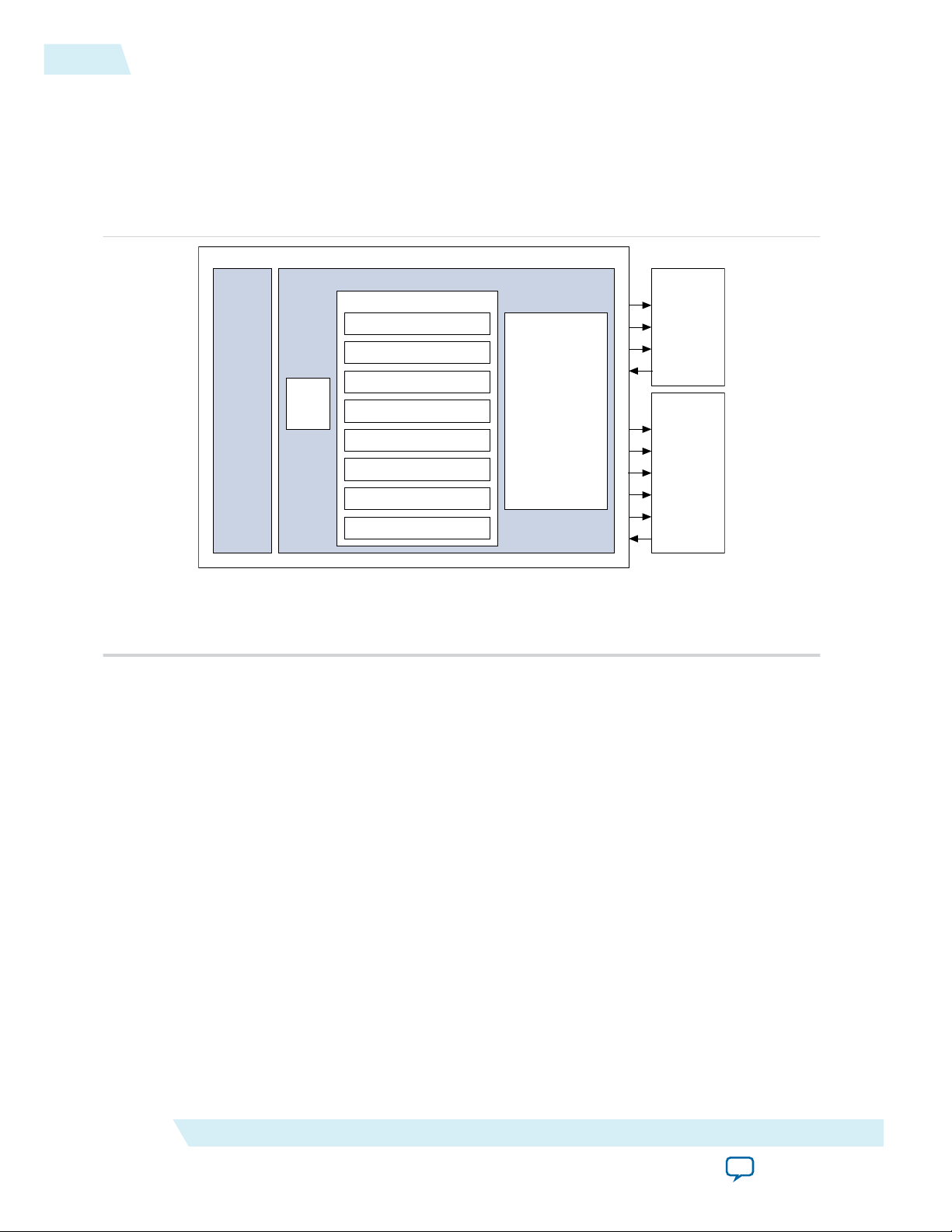
Device Family Support
This figure shows that you can use the Altera ASMI Parallel IP core to access the general purpose memory
portion of the EPCS/EPCQ/EPCQ-L devices through the supported Altera devices.
Caution: Altera recommends you to be cautious when accessing the configuration memory in the EPCS/
EPCQ/EPCQ-L device to avoid corrupting the configuration bits.
Example 1: Accessing General Purpose Memory in Altera Devices
UG-ALT1005
2014.12.15
Device Family Support
Altera Corporation
Related Information
• Introduction to Altera IP Cores
For more information about Altera IP cores
• Active Serial Configuration
For more information about AS configuration
• Serial Configuration Devices Datasheet
For more information about EPCS devices
• Quad-Serial Configuration (EPCQ) Device Datasheet
• EPCQ-L Serial Configuration Devices Datasheet
• Altera Configuration Device
The Altera ASMI Parallel IP core is available for all Altera device families supported by the Quartus II
software except the MAX® series.
For more information about features, memory array organization, and operation codes of the EPCS
device
Altera ASMI Parallel IP Core User Guide
Send Feedback
Page 3
Altera ASMI Parallel
clkin (1)
fast_read (9), (4)
rden (1)
read_sid
(2), (5)
read_status
(1)
write
(1)
datain[]
(1)
shift_bytes
(1)
sector_protect (1)
sector_erase
(1)
bulk_erase
(11)
wren
(1)
read_rdid
(1), (6)
addr[]
(1)
dataout[] (1)
busy (1)
data_valid (1)
status_out[] (1)
illegal_write (1)
illegal_erase (1)
read_address[] (1)
rdid_out[] (1), (6)
epcs_id[] (2), (5)
read
(1), (4)
read_dummyclk
(3), (7)
reset
(1)
asmi_dataout[] (1)
asmi_dclk (1)
asmi_scein (1)
asmi_sdoin[] (1)
asmi_dataoe[] (1)
en4b_addr
(3), (8)
ex4b_addr (3), (8)
Applicable for EPCS/EPCQ/EPCQ-L devices.
Applicable for EPCS devices only.
Applicable for EPCQ/EPCQ-L devices only.
The read and fast_read signals cannot be present simultaneously.
EPCS128 does not support the read_sid and epcs_id signals.
EPCS1 and EPCS4 do not support read_rdid and rdid_out signals.
The read_dummyclk is available only when you select the Use ‘fast_read’ port option.
The en4b_addr and ex4b_addr signals are supported only for EPCQ256/EPCQ-L256 or larger devices.
Applicable for all EPCS/EPCQ/EPCQ-L devices, except for EPCS1 and EPCS4 devices.
die_erase
(12)
sce[2..0]
Applicable for Arria 10 devices only.
Applicable for all EPCS/EPCQ/EPCQ-L devices, except for EPCQ512, EPCQ-L512 and EPCQL-1024.
Applicable for EPCQ-L512 and EPCQL-1024 devices.
(1)
(2)
(3)
(4)
(5)
(6)
(7)
(8)
(9)
(10)
(11)
(12)
(13)
Applicable for Arria 10 devices only.
(13)
UG-ALT1005
2014.12.15
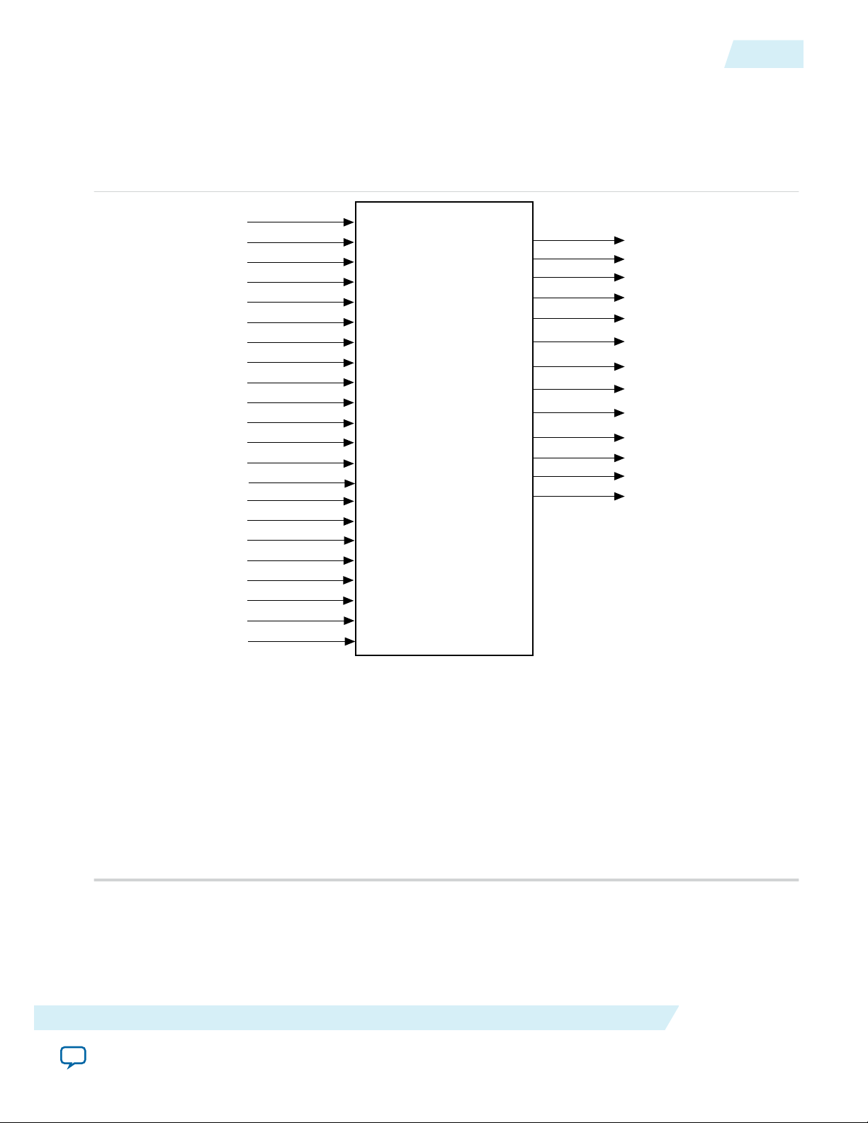
Ports and Parameters
This figure shows a typical block diagram of the Altera ASMI Parallel IP core.
Figure 1: Altera ASMI Parallel Block Diagram
Ports and Parameters
3
Altera ASMI Parallel IP Core User Guide
Send Feedback
Altera Corporation
Page 4

4
Parameters
Parameters
Table 1: Parameter Settings
Parameter Legal Values Descriptions
UG-ALT1005
2014.12.15
Currently selected device
family
Arria GX,
Arria V GZ,
Arria II GX,
Arria II GZ,
Arria V,
Cyclone,
Cyclone II,
Cyclone III,
Cyclone III LS,
Cyclone IV E,
Cyclone IV GX,
Cyclone V,
HardCopy III,
HardCopy IV,
Stratix II,
• Specifies the device family you intend to use. Use this
parameter for modeling and behavioral simulation
purposes, as each device family has its own ASMI
primitive.
Stratix II GX,
Stratix III,
Stratix IV,
Stratix V,
Arria 10
Altera Corporation
Altera ASMI Parallel IP Core User Guide
Send Feedback
Page 5

UG-ALT1005
2014.12.15
Parameter Legal Values Descriptions
Parameters
5
Configuration device
EPCS1,
type
EPCS4,
EPCS16,
EPCS64,
EPCS128,
EPCQ16,
EPCQ32,
EPCQ64,
EPCQ128,
EPCQ256,
EPCQ512,
EPCQ-L256,
EPCQ-L512,
EPCQ-L1024
Use ‘read_sid’ port —
• Specify the EPCS/EPCQ/EPCQ-L type you want to use.
• The default value is EPCS4.
• Enables the ability to read the silicon ID of the EPCS
device with an active-high read_sid input signal.
When this signal is asserted, the IP core reads the
silicon ID of the EPCS device. After reading the silicon
ID, the 8-bit silicon ID appears on the epcs_
id[7..0]signal until the device resets.
• This option is available only for EPCS1, EPCS4,
EPCS16, and EPCS64 devices.
Use ‘read_status’ port —
Altera ASMI Parallel IP Core User Guide
Send Feedback
• Enables the ability to read the port status using an
active-high input signal named read_status. When
this signal is asserted, the IP core reads the EPCS/
EPCQ/EPCQ-L status register. As the status register is
read, the 8-bit value appears on the status_
out[7..0]signal.
• This option is available for all EPCS/EPCQ/EPCQ-L
devices.
Altera Corporation
Page 6

6
Parameters
Parameter Legal Values Descriptions
UG-ALT1005
2014.12.15
Use ‘read_rdid’ and
—
‘rdid_out’ ports
Enable write operation —
• Enables the ability to read the memory capacity ID of
the EPCS/EPCQ/EPCQ-L device with an active-high
input signal named read_rdid. When this signal is
asserted, the IP core reads the memory capacity ID of
the EPCS/EPCQ/EPCQ-L device. The 8-bit ID appears
on the rdid_out[7..0]signal until the device resets.
• This option is available for all devices, except for
EPCS1 and EPCS4.
• Enables the ability to write to the EPCS/EPCQ/EPCQL device with an active-high input signal named write.
When this port is asserted, the IP core writes the data
from the datain[7..0]signal (for single-byte write) or
from the page-write buffer (for page-write) to the
address that appears on the addr[23..0]port, and to
subsequent addresses for page-write. For EPCQ256/
EPCQ-L256 or larger devices, the width of the addr
and read_address signals is 32 bit.
• In page-write mode, you must use the shift_byte
signal to shift in data bytes before asserting the write
signal.
• This option is available for all EPCS/EPCQ/EPCQ-L
devices.
Use ‘wren’ port —
• Enables write and erase operations to the EPCS/EPCQ/
EPCQ-L memory with an active-high input signal
named wren. If this signal is asserted, the write and
erase operations are enabled, and disabled if the signal
is deasserted. If you are not using the wren signal, all
write and erase operations are automatically enabled
when the command appears on the relevant IP core
input port. The affected commands are write, sector
protect, bulk erase, and sector erase.
• This option is only available when you turn on the
Enable write operation, Use ‘sector protect’ port or
die erase port, Use ‘bulk erase’ port, or Use ‘sector
erase’ port option.
• This option is available for all EPCS/EPCQ/EPCQ-L
devices.
Altera Corporation
Altera ASMI Parallel IP Core User Guide
Send Feedback
Page 7

UG-ALT1005
2014.12.15
Parameter Legal Values Descriptions
Parameters
7
Write mode —
Use ‘fast_read’ port —
• This option is only available when you turn on the
Enable ‘write’ operation option.
• When you select this option, the Altera ASMI Parallel
IP core defines two parameters, which are PAGE_SIZE
and PORT_SHIFT_BYTES for the following writing
mode to the EPCS/EPCQ/EPCQ-L device:
Single byte write: PAGE_SIZE = 1, PORT_SHIFT_
BYTES = PORT_UNUSED
Page write: PAGE_SIZE = 1 to 256, if 1 then PORT_
SHIFT_BYTES = PORT_UNUSED, else PORT_USED
Store ‘page write’ data in logic elements.
• Enables the ability to perform a fast read operation
with an active-high input signal named fast_read.
When this signal is asserted, the IP core performs a fast
read from the memory address that appears on the
addr[23..0]signal. Each data byte appears on the
dataout[7..0] signal as it is read. For EPCQ256/
EPCQ-L256 or larger devices, the width of the addr
and read_address signals is 32 bit.
• The fast_read signal supports single-byte fast read
and sequential fast read. If a write or erase operation is
in progress (the busy signal is asserted), the fast read
command is ignored. The fast read operation occurs
only when allowed by the rden signal.
• This option is available for all EPCS/EPCQ/EPCQ-L
devices, except for EPCS1 and EPCS4 devices.The fast
read operation replaces the normal settings.
Altera ASMI Parallel IP Core User Guide
Send Feedback
Altera Corporation
Page 8

8
Parameters
Parameter Legal Values Descriptions
UG-ALT1005
2014.12.15
Choose I/O mode STANDARD,
DUAL, QUAD
Read device dummy clock —
• The following commands are the instructions from the
EPCQ/EPCQ-L extended serial peripheral interface
(SPI) protocol which uses multiple data lines:
Dual Fast Read (Dual Input/Output Fast Read)
Quad Fast Read (Quad Input/Output Fast Read)
Dual Write (Dual Input Extended Fast Program)
Quad Write (Quad Input Extended Fast Program)
• These commands are combined into the following
ports:
Fast read port – fast read (x1), dual fast read and quad
fast read
Write port – write (x1), dual write and quad write
• You can choose which I/O mode to use, the choices are
Standard (x1), Dual (x2) or Quad (x4) mode.
• This option is only available for EPCQ/EPCQ-L
devices.
• This option is disabled by default and the IP core
generates the design file as per usual.
• To perform fast read operation, align the dummy
cycles of EPCQ/EPCQ-L devices with Altera ASMI
Parallel designated value.
• When enabling this option, the read_dummyclk input
pin is created. The Altera ASMI Parallel IP core reads
the dummy clock stored in a non-volatile configuration
register of a flash at the beginning of the operation.
• When the signal is asserted high, the Altera ASMI
Parallel IP core reads the dummy clock in the volatile
configuration register of the flash. The value is held till
the next signal is asserted or when the device resets.
• This option is available for EPCQ/EPCQ-L devices
only.
Altera Corporation
Altera ASMI Parallel IP Core User Guide
Send Feedback
Page 9

UG-ALT1005
2014.12.15
Parameter Legal Values Descriptions
Parameters
9
Use ‘sector_protect’ port —
Use ‘bulk_erase’ port —
Use ‘sector_erase’ port —
• Enables the ability to protect sectors in the EPCS/
EPCQ/EPCQ-L device from write and erase operations
with an active-high input port named sector_
protect. When this port is asserted, the IP core reads
the block protection code value on the
datain[7..0]signal and writes it to the EPCS/EPCQ/
EPCQ-L status register. To protect specific memory
sectors, you must send their block protection code to
the datain[7..0] signal.
• This option is available for all EPCS/EPCQ/EPCQ-L
devices.
• Enables the ability to erase the entire memory of the
EPCS/EPCQ/EPCQ-L256 device, including the
configuration data portion with an active-high input
signal named bulk_erase. When this signal is asserted,
the IP core implements a full erase that sets the entire
memory bits of the EPCS/EPCQ/EPCQ-L256 device to
a value of one.
• This option is available for all EPCS/EPCQ devices.
• Enables the ability to erase a certain sector in the
EPCS/EPCQ memory with an active-high input signal
named sector_erase. When the signal is asserted, the
IP core implements a full erase of the sector. The value
of the addr[23..0]signal indicates the sector to erase.
For EPCQ256/EPCQ-L256 or larger devices, the width
of the addr and read_address signals is 32 bit.
• This option is available for all EPCS/EPCQ/EPCQ-L
devices.
Use ‘die_erase’ port —
Altera ASMI Parallel IP Core User Guide
Send Feedback
• Enables the ability to erase each die in your device.
When the signal is asserted, the IP core implements a
full erase of a single die in your device. You need to
issue the erase die operation twice for EPCQ-L512
device and four times for the EPCQ-L1024.
• This option is available for Arria 10 devices with
EPCQL-512 and EPCQL-1024.
Altera Corporation
Page 10

10
Parameters
Parameter Legal Values Descriptions
UG-ALT1005
2014.12.15
Use ‘read_address’ port —
Use 'ex4b_addr’ —
• This signal holds the address from which data is being
read. This signal works together with the
dataout[7..0]signal. As data appears on
dataout[7..0], the address from which the data byte
was read appears on the read-address output port. For
EPCQ256/EPCQ-L256 or larger devices, the width of
the addr and read_address signals is 32 bit. For other
devices, the width of the addr and read_address
signals is 24 bit.
• This option is available for all EPCS/EPCQ/EPCQ-L
devices.
• To exit the 4-byte addressing mode when you use an
EPCQ256/EPCQ-L256 or larger devices, pull the
WREN signal high, followed by at least one clock cycle.
If WREN signal is zero, the 4-byte addressing mode
exit operation will not be carried out even though the
ex4b_addr is high. After the IP core receives the
command, the IP core asserts the busy signal to
indicate that the exit operation is in progress.
• Only applicable for EPCQ256/EPCQ-L256 or larger
devices.
Altera Corporation
Altera ASMI Parallel IP Core User Guide
Send Feedback
Page 11

UG-ALT1005
2014.12.15
Parameter Legal Values Descriptions
Parameters
11
Disable dedicated Active
Serial interface
—
• This option is disabled by default and the IP core
generates the design file as per usual.
• The Altera ASMI Parallel IP core instantiates the ASMI
block internally and connects to the block automati‐
cally.
• The IP core creates the following input/output pins
when you enable this option:
asmi_dataout,
asmi_dclk,
asmi_scein,
asmi_sdoin,
asmi_dataoe.
• When you enable this option, the Altera ASMI Parallel
IP core will not instantiate ASMI block automatically,
and all signals to interface with ASMI block are routed
to the top level of your design. You must then
instantiate the ASMI block externally, and assign the
ASMI ports in the Altera ASMI Parallel IP core to the
dedicated pins location.
• The CLI parameter to disable this option is USE_
ASMIBLOCK=ON.
• This option is available for all EPCS/EPCQ/EPCQ-L
devices.
Related Information
• Introduction to Altera IP Cores
For more information about starting the IP Parameter Editor
• Quad-Serial Configuration (EPCQ) Devices Datasheet
For the designated Altera ASMI Parallel dummy cycles values
• on page 20
For more information about the Use ‘read_sid’ port parameter
• on page 29
For more information about the Use ‘read_status’ port parameter
• on page 19
For more information about the Use ‘read_rdid’ and ‘rdid_out’ ports parameter
• on page 26
For more information about the Enable write operation parameter
• on page 23
For more information about the Use ‘fast_read’ port parameter
• on page 21
For more information about the Use ‘sector_protect’ port parameter
Altera ASMI Parallel IP Core User Guide
Altera Corporation
Send Feedback
Page 12

12
Input Ports
• on page 31
For more information about the Use ‘bulk_erase’ port parameter
• on page 30
For more information the Use 'sector_erase' port parameter. The value of the signal for the Use
'sector_erase' port parameter is a valid address in the sector.
Input Ports
This table lists the input ports for the Altera ASMI Parallel IP core.
Table 2: Input Ports
Port Condition Size Descriptions
UG-ALT1005
2014.12.15
addr[] Required 24 or
32 bit
Contains the value of the EPCS/EPCQ/EPCQ-L memory
address to be read from, written to, and erased from.
For EPCQ256/EPCQ-L256 or larger devices, the width of
the addr[] is 32 bit.
asmi_dataout[] Optional 1 bit Input port to feed data from EPCS/EPCQ/EPCQ-L device if
select the Disable dedicated Active Serial interface option.
If you are using Arria® V, Cyclone® V, Stratix® V, or Arria
10 devices, then the bit size is 4 bit.
bulk_erase Optional 1 bit Active-high port that executes the bulk erase operation. If
asserted, the IP core performs a full-erase operation that sets
all memory bits of the EPCS/EPCQ/EPCQ-L256 device to
‘1’, which includes the general purpose memory of the
EPCS/EPCQ/EPCQ-L device.
clkin Required 1 bit Input clock port for the ASMI block. In general, the clkin
signal must toggle at the appropriate frequency range at all
times. The IP core uses the signal to feed the EPCS/EPCQ/
EPCQ-L device and to perform internal processing.
datain[] Optional 8 bit Parallel input data of 1-byte length for write and sector
protect operations.
en4b_addr Required 1 bit When you select EPCQ256/EPCQ-L256 or larger devices as
your configuration device, address width will change from
0..23 to 0..31. EPCQ256 supports Dual and Quad data
width.
Altera Corporation
If you select EPCQ256/EPCQ-L256 or larger devices as your
configuration device, this port is required.
Altera ASMI Parallel IP Core User Guide
Send Feedback
Page 13

UG-ALT1005
2014.12.15
Input Ports
Port Condition Size Descriptions
ex4b_addr Optional 1 bit To exit the 4-byte addressing mode when you use an
EPCQ256/EPCQ-L256 or larger devices, pull the WREN
signal high, followed by at least one clock cycle. If WREN
signal is zero, the 4-byte addressing mode exit operation will
not be carried out even though the ex4b_addr is high. After
the IP core receives the command, the IP core asserts the
busy signal to indicate that the exit operation is in progress.
If you select EPCQ256/EPCQ-L256 or larger devices as your
configuration device, this port is required.
fast_read Optional 1 bit Active-high port that executes the fast read operation. If
asserted, the IP core performs a fast read operation from a
memory address value that appears on the addr[23..0]
port. For EPCQ256/EPCQ-L256 or larger devices, the width
of the addr and read_address signals is 32 bit.
Use the fast_read port together with the rden port.
rden Required 1 bit Active-high port that allows read and fast read operations to
be performed as long as it stays asserted. This port is only
for Altera ASMI Parallel IP core and not the configuration
device.
13
read Required 1 bit Active-high port that executes the read operation. If
asserted, the IP core performs a read operation from a
memory address value that appears on the addr[23..0]
port. For EPCQ256/EPCQ-L256 or larger devices, the width
of the addr and read_address signals is 32 bit.
Use the read port together with the rden port. The read
port is disabled if the fast_read port is used.
read_dummyclk Optional 1 bit By pulling high the read_dummyclk signal for at least one
clock cycle, the Altera ASMI Parallel IP core reads the
device dummy cycles from a volatile register and stores the
value in a register. You can use the stored value for fast read
operation without changing the dummy cycles (if the
dummy cycles is different from designated value). The
stored value is hold until the next high read_dummyclk
signal or power cycle of FPGA.
When you enable this option, the dummy clock value is read
from a non-volatile register of an EPCQ/EPCQ-L device, by
default. If asserted high, the dummy clock value changes to
the dummy clock value read from a volatile register.
When you disable this option, the dummy clock used in the
IP core is as per default in the EPCQ/EPCQ-L device.
read_rdid
Altera ASMI Parallel IP Core User Guide
Send Feedback
Optional 1 bit Active-high port that executes the read memory capacity ID
operation. If asserted, the IP core proceeds to read the
memory capacity ID of the EPCS/EPCQ/EPCQ-L device,
and the value of the memory capacity ID appears at the
rdid_out[7..0] port.
Altera Corporation
Page 14

14
Input Ports
Port Condition Size Descriptions
read_sid Optional 1 bit Active-high port that executes the read silicon ID operation.
If asserted, the IP core proceeds to read the silicon ID of the
EPCS device, and the value of the silicon ID appears at the
epcs_id[7..0] port.
read_status Optional 1 bit Active-high port that executes the read EPCS/EPCQ/EPCQ-
L status register operation. If asserted, the IP core reads the
status register of the EPCS/EPCQ/EPCQ-L device, and
outputs the value at the status_out[7..0] port. You can
use the read_status port to determine which memory
sector on the EPCS/EPCQ/EPCQ-L device is read-only.
reset Required 1 bit To reset all counters and registers in the Altera ASMI
Parallel IP core (not the EPCS/EPCQ/EPCQ-L devices), pull
the reset signal high for at least two clock cycles.
The reset signal is asserted regardless of busy status, hence,
do not assert the reset signal whenever the Altera ASMI
Parallel IP core is running.
After asserting the reset signal, allow two clock cycles to
reset the circuit before sending a new signal.
UG-ALT1005
2014.12.15
Default value of the reset port is 0.
sector_erase Optional 1 bit Active-high port that executes the sector erase operation. If
asserted, the IP core starts erasing the memory sector on the
EPCS/EPCQ/EPCQ-L device based on the memory address
value at the addr[23..0] port. The value is a valid memory
address in the sector to be erased. For EPCQ256/EPCQL256 or larger devices, the width of the addr and read_
address signals is 32 bit.
sector_protect Optional 1 bit Active-high port that executes the sector protect operation.
If asserted, the IP core takes the value of the datain[7..0]
port and writes to the EPCS/EPCQ/EPCQ-L status register.
The status register contains the block protection bits that
represent the memory sector to be protected.
shift_bytes Optional 1 bit Active-high port that shifts data bytes during the write
operation. You must use this port together with the write
port during the page-write operation. The IP core samples
and shifts the data in the datain[7..0] port at the rising
edge of the clkin signal, as long as the shift_bytes signal
is asserted. Continue shifting the required bytes into the
EPCS/EPCQ/EPCQ-L device until the IP core finishes
sampling and storing the data internally.
Altera Corporation
Altera ASMI Parallel IP Core User Guide
Send Feedback
Page 15

UG-ALT1005
2014.12.15
Input Ports
Port Condition Size Descriptions
wren Optional 1 bit Active-high port that allows write and erase operations to be
performed as long as it stays asserted. If the IP core does not
generate this port, the IP core automatically allows all write
and erase operations. Use this port with the following ports:
• write
• sector_protect
• bulk_erase
• sector_erase
• die_erase
write Optional 1 bit Active-high port that executes the write operation. If
asserted, the IP core writes the data from the datain[7..0]
port (for single-byte write), or from the page-write buffer
(for page-write), to the memory address specified in the
addr[23..0] port (and to the subsequent addresses for page
write operation). For EPCQ256/EPCQ-L256 or larger
devices, the width of the addr and read_address signals is
32 bit.
In page-write operation, you must use the shift_bytes
port to shift in data bytes before asserting the write port.
15
sce[] Optional 3 bit Select targeted flash for desired operation by controlling
FPGA nCSO[2..0] pin
• 3'b000 (default value)/ 3'b001: select flash connected to
nCSO[0]
• 3'b010: select flash connected to nCSO [1]
• 3'b100: select flash connected to nCSO [2]
sce[] is only available for Arria 10 devices
Related Information
• on page 33
For more information about en4b_addr signal
• on page 23
For more information about the fast read operation
• on page 18
For more information about read, fast read, write and erase operations
• on page 22
For more information about the read operation
• on page 19
For more information about the read memory capacity ID operation
• on page 20
For more information about the read silicon ID operation
• on page 29
For more information about the read EPCS/EPCQ status register operation
• on page 30
For more information about the sector erase operation
Altera ASMI Parallel IP Core User Guide
Send Feedback
Altera Corporation
Page 16

16
Output Ports
• on page 21
For more information about the sector protect operation
• on page 26
For more information about the write operation
• on page 26
For more information about the write operation
Output Ports
This table lists the output ports for the Altera ASMI Parallel IP core.
Table 3: Output Ports
Port Condition Size Descriptions
asmi_dclk Optional 1 bit Provides clock signal to the EPCS/EPCQ/EPCQ-L device
when you select the Disable dedicated Active Serial
interface option.
UG-ALT1005
2014.12.15
asmi_scein Optional 1 or 3
Provides the ncs signal to the EPCS/EPCQ/EPCQ-L device
bit
when you select the Disable dedicated Active Serial
interface option.
If you are using Arria 10 devices, the bit size is 3.
asmi_sdoin Optional 1 or 4
Provides data signal to the EPCS/EPCQ/EPCQ-L device
bit
when you select the Disable dedicated Active Serial
interface option.
If you are using Arria V, Cyclone V, Stratix V, or Arria 10
devices, then the bit size is 4.
asmi_dataoe Optional 1 or 4
Provides data input/output control signal to the EPCS/
bit
EPCQ/EPCQ-L device when you the Disable dedicated
Active Serial interface option.
If you are using Arria V, Cyclone V, Stratix V, or Arria 10
devices, then the bit size is 4.
busy Required 1 bit Indicates the IP core is performing a valid operation. The
busy signal goes high when the IP core is executing a valid
operation, and goes low after the operation.
data_valid Required 1 bit Indicates that the dataout[7..0] port contains a valid data
byte read from the EPCS/EPCQ/EPCQ-L memory. Sample
the dataout[7..0]port only when the data_valid signal is
high.
dataout[] Required 8 bit Contains the data byte read from the EPCS/EPCQ/EPCQ-L
Altera Corporation
memory during read operation. This port holds the value of
the last data byte read until the device resets, or until the IP
core carries out a new read operation. Sample the
dataout[7..0] port only when the data_valid signal is
high.
Altera ASMI Parallel IP Core User Guide
Send Feedback
Page 17

UG-ALT1005
2014.12.15
Output Ports
Port Condition Size Descriptions
epcs_id[] Optional 8 bit Contains the silicon ID of the EPCS device after the read
silicon ID operation. This port holds the value of the silicon
ID until the device resets. Sample the epcs_id[7..0] port
after the busy signal goes low.
illegal_erase Optional 1 bit Indicates that an erase instruction has been set to a
protected sector on the EPCS/EPCQ/EPCQ-L memory. This
port is required when you specify the sector_erase port,
bulk_erase port, or die_erase port. The illegal_erase
signal goes high to indicate that the IP core has cancelled the
erase instruction. The signal pulses high for two clock cycles
—one clock cycle before, and one clock cycle after the busy
signal goes low. Monitor this port to detect the status of an
erase operation.
illegal_write Optional 1 bit Indicates that a write instruction is targeting a protected
sector on the EPCS/EPCQ/EPCQ-L memory. This port is
required when you specify the write port. The illegal_
write signal goes high to indicate that the IP core has
cancelled a write instruction. The signal pulses high for two
clock cycles—one clock cycle before, and one clock cycle
after the busy signal goes low. Monitor this port to detect
the status of a write operation.
17
rdid_out[] Optional 8 bit Contains the memory capacity ID of the EPCS/EPCQ/
EPCQ-L device after the read memory capacity ID
operation is completed. This port holds the value until the
device resets. Sample the rdid_out[7..0] port after the
busy signal goes low.
read_address[] Optional 24 or
32 bit
Contains the memory address of the EPCS/EPCQ/EPCQ-L
to be read from. Use this port together with the
dataout[7..0]port.
For EPCQ256/EPCQ-L256 or larger devices, the width of
the addr and read_address signals is 32 bit.
status_out[] Optional 8 bit Contains the value of the EPCS/EPCQ/EPCQ-L status
register after the read status register operation is completed.
This port holds the value until you execute another reading
status register operation, or until you reset the device. To
obtain the most recent value of the status register, you must
perform a read status register operation before sampling the
status_out[7..0] port. Sample the port only after the
busy signal goes low.
Related Information
• on page 26
For more information about the write operation
• on page 23
For more information about the read operation
• on page 20
For more information about the read silicon ID operation
Altera ASMI Parallel IP Core User Guide
Send Feedback
Altera Corporation
Page 18

acds
quartus - Contains the Quartus II software
ip - Contains the Altera IP Library and third-party IP cores
altera - Contains the Altera IP Library source code
<IP core name> - Contains the IP core source files
18
Installing and Licensing IP Cores
• on page 18
For more information about the erase operation
• on page 26
For more information about the write operation
• on page 19
For more information about the read memory capacity ID operation
• on page 29
For more information about the read status register operation
Installing and Licensing IP Cores
The Altera IP Library provides many useful IP core functions for production use without purchasing an
additional license. You can evaluate any Altera® IP core in simulation and compilation in the Quartus® II
software using the OpenCore® evaluation feature. Some Altera IP cores, such as MegaCore® functions,
require that you purchase a separate license for production use. You can use the OpenCore Plus feature to
evaluate IP that requires purchase of an additional license until you are satisfied with the functionality and
performance. After you purchase a license, visit the Self Service Licensing Center to obtain a license
number for any Altera product.
Figure 2: IP Core Installation Path
UG-ALT1005
2014.12.15
Note: The default IP installation directory on Windows is <drive>:\altera\<version number>; on Linux it is
<home directory>/altera/ <version number>.
Related Information
• Altera Licensing Site
• Altera Software Installation and Licensing Manual
Altera ASMI Parallel IP Core Operations and Timing Requirements
Understanding the operations help you to implement the Altera ASMI Parallel IP core with the functions
you desire.
The following shows the supported operations listed from the highest priority to the lowest. The IP core
executes the operation with the highest priority when more than one operation are requested at once. The
rest is ignored.
Altera Corporation
Altera ASMI Parallel IP Core User Guide
Send Feedback
Page 19

UG-ALT1005
2014.12.15
Read Memory Capacity ID from the EPCS/EPCQ/EPCQ-L Device
19
• Read Memory Capacity ID from the EPCS/EPCQ/EPCQ-L Device
• Read Silicon ID from the EPCS Device
• Protect a Sector on the EPCS/EPCQ/EPCQ-L Device
• Read Data from the EPCS/EPCQ/EPCQ-L Device
• Fast Read Data from the EPCS/EPCQ/EPCQ-L Device
• Write Data to the EPCS/EPCQ/EPCQ-L Device
• Read Status Register of the EPCS/EPCQ/EPCQ-L Device
• Erase Memory in a Specified Sector on the EPCS/EPCQ/EPCQ-L256 Device
• Erase Memory in Bulk on the EPCS/EPCQ Device
• Erase Memory in Specified Die on EPCQ-L512 and EPCQ-L1024
• Enable 4-byte Addressing Operation for an EPCQ256/EPCQ-L256 or larger devices
• 4-byte Addressing Exit Operation for an EPCQ256/EPCQ-L256 or larger devices
Note: The timing diagrams show the expected results in the hardware and are not the actual results from
the simulation.
The general timing requirement for all operations is the clkin signal must toggle at the appropriate
frequency range at all times. The IP core uses the clkin signal to feed the EPCS/EPCQ/EPCQ-L device
and to perform internal processing. For a read operation, the clkin signal can toggle at a maximum
frequency of 20 MHz. For a fast read operation, the clkin signal can toggle at a maximum frequency of
25 MHz.
Note:
Altera recommends that you check the busy signal before sending a new command. When the
busy signal is deasserted, allow two clock cycles before sending a new signal. This delay allows the
circuit to reset itself before executing the next command.
Read Memory Capacity ID from the EPCS/EPCQ/EPCQ-L Device
Use the read_rdid signal to instruct the IP core to read the memory capacity ID from the EPCS/EPCQ/
EPCQ-L device.
Figure 3: Reading Memory Capacity ID
This figure shows an example of the latency when the Altera ASMI Parallel IP core is executing the read
command. The latency shown does not correctly indicate the true processing time. The latency only
shows the command.
The IP core registers the read_rdid signal on the rising edge of the clkin signal. After the IP core
registers the read_rdid signal, the IP core asserts the busy signal to indicate that the read
command is in progress.
Ensure that the memory capacity ID appears on the rdid_out[7..0] signal before the busy
signal is deasserted. This allows you to sample the rdid_out[7..0] signal as soon as the busy
signal is deasserted.
Altera ASMI Parallel IP Core User Guide
Send Feedback
Altera Corporation
Page 20

20
Read Silicon ID from the EPCS Device
The rdid_out[7..0] signal holds the value of the memory capacity ID until the device resets.
Therefore, you must execute this read command only once.
Note: To meet setup and hold time requirements, assert the read_rdid signal any time
between the rising edges of the clkin signal, and keep the read_rdid signal
asserted for at least one full clock cycle. Ensure that the read_rdid signal assertion
does not coincide with the rising edges of the clkin signal.
If you keep the read_rdid signal asserted while the busy signal is deasserted after the IP core has
finished processing the read command, the IP core re-registers the read_rdid signal as a value of
one and carries out the command again. Therefore, you must deassert the read_rdid signal
before the busy signal is deasserted.
Read Silicon ID from the EPCS Device
Use the read_sid signal to instruct the IP core to read the silicon ID from the EPCS device.
Figure 4: Reading Silicon ID
This figure shows an example of the latency when the Altera ASMI Parallel IP core is executing the read
command. The latency shown does not correctly indicate the true processing time. The latency only
shows the command.
UG-ALT1005
2014.12.15
The IP core registers the read_sid signal on the rising edge of the clkin signal. After the IP core
registers the read_sid signal, it asserts the busy signal to indicate that the read command is in
progress.
Ensure that the silicon ID appears on the epcs_id[7..0] signal before the busy signal is
deasserted. Therefore, you can sample the epcs_id[7..0] signal as soon as the busy signal is
deasserted.
The epcs_id[7..0] signal holds the value of the silicon ID until the device resets. Therefore, you
must execute this command only once.
Note:
If you keep the read_sid signal asserted while busy signal is deasserted and the IP core has
finished processing the read command, the IP core re-registers the read_sid signal as a value of
one and carries out another read command. Therefore, before the IP core deasserts the busy
signal, you must deassert the read_sid signal.
Altera Corporation
To meet setup and hold time requirements, assert the read_sid signal any time
between the rising edges of the clkin signal, and keep the read_sid signal
asserted for at least one full clock cycle. Ensure that the read_sid signal assertion
does not coincide with the rising edges of the clkin signal.
Altera ASMI Parallel IP Core User Guide
Send Feedback
Page 21

UG-ALT1005
2014.12.15
Protect a Sector on the EPCS/EPCQ/EPCQ-L Device
Use the sector_protect signal to instruct the IP core to protect a sector on the EPCS/EPCQ/EPCQ-L
device.
Figure 5: Protecting a Sector
This figure shows an example of the latency when the Altera ASMI Parallel IP core is executing the sector
protect command. The latency shown does not correctly reflect the true processing time. It shows the
command only.
Protect a Sector on the EPCS/EPCQ/EPCQ-L Device
21
This command writes the EPCS/EPCQ/EPCQ-L status register to set the block protection bits.
The block protection bits show which sectors are protected from write or erase, and provide
protection in addition to that provided by the wren signal.
You can set the block protection bits in the EPCS/EPCQ/EPCQ-L status register to protect those
sectors that contain configuration data, and are not intended for general-purpose memory usage.
Ensure that the 8-bit code is available on the datain[7..0] signal before asserting the
sector_protect and wren signals. The IP core registers the sector_protect signal at the
positive edge of the clkin signal.
The IP core asserts the busy signal as soon as it receives the sector_protect signal. The busy
signal remains asserted while the EPCS/EPCQ/EPCQ-L status register is written.
If the wren signal has a value of zero, the IP core will not carry out the sector_protect signal,
and the busy signal remains deasserted.
Note:
If you keep the wren and sector_protect signals asserted while the busy signal is
deasserted after the IP core has finished processing the sector protect command,
the IP core re-registers the wren and sector_protect signals as a value of one and
carries out another write status register operation. Therefore, before the IP core
deasserts the busy signal, you must deassert the sector_protect signal.
The IP core uses only bits 2 to 3, or 2 to 4 for EPCS devices, and 2 to 5, or 2 to 6 for EPCQ/EPCQL devices out of the 8 bits for block protection. The rest of the bits have other meanings for the
ASMI operation, and cannot be overwritten by the sector protect operation. Whenever the input
address is in a protected sector, the IP core omits the operation and the busy signal remains
deasserted.
Altera ASMI Parallel IP Core User Guide
Send Feedback
Altera Corporation
Page 22

22
Read Data from the EPCS/EPCQ/EPCQ-L Device
Related Information
• Serial Configuration Devices Datasheet
For more information about the block protection level for EPCQ devices. Every devices have different
block protection level.
• EPCQ-L Serial Configuration Devices Datasheet
For more information about the block protection level for EPCQ-L devices. Every devices have
different block protection level.
Read Data from the EPCS/EPCQ/EPCQ-L Device
Use the read signal to instruct the IP core to read data from the EPCS/EPCQ/EPCQ-L device. The Altera
ASMI Parallel IP core supports two types of read data operation: multiple-byte and single-byte read.
Figure 6: Reading Multiple-Byte
This figure shows an example of the latency when the Altera ASMI Parallel IP core is executing multiplebyte read command. The latency shown does not correctly indicate the true processing time. It shows the
command only.
UG-ALT1005
2014.12.15
Figure 7: Reading Single-Byte
This figure shows an example of single-byte read command. The latency shown does not correctly
indicate the true processing time. It shows the command only.
The IP core registers the read signal on the rising edge of the clkin signal. After the IP core
receives the read command, it asserts the busy signal to indicate that the read command is in
progress.
Ensure that the read address appears on the addr[23..0] signal before asserting the read signal.
The rden signal must also be asserted to enable the read operation.
Altera Corporation
Altera ASMI Parallel IP Core User Guide
Send Feedback
Page 23

UG-ALT1005
2014.12.15
Fast Read Data from the EPCS/EPCQ/EPCQ-L Device
The first data byte then appears on the dataout[7..0] signal. The IP core then asserts the
data_valid signal for one clock cycle, which indicates that the dataout[7..0]signal contains a
new valid data.
If you enable the read_address[23..0] port in the IP parameter editor, the port reflects the
memory address for each data byte that appears on dataout[7..0] signal.
If you want to continue reading sequential data from the EPCS/EPCQ/EPCQ-L device, the rden
signal must remain asserted. This condition allows you to read every memory address from the
EPCS/EPCQ/EPCQ-L device with a single read command.
For every eight clkin signal clock cycles, a new data byte from the next address appears on the
dataout[7..0] signal with its corresponding memory address on the read_address[23..0]
signal. The data_valid signal is asserted for one clock cycle after the new data byte is out on the
dataout[7..0] signal. Use the data_valid signal as an indication to capture the new data byte.
After the second-to-last byte of data to be read appears on the dataout[7..0] signal, and the
data_valid signal is asserted, deassert the rden signal to indicate the end of the read command.
A new byte from the next address then appears on the dataout[7..0] signal, and the
data_valid signal is reasserted before the IP core stops processing. Only then does the IP core
deassert the busy signal.
For a single-byte read, simply assert the rden signal for one clock cycle in conjunction with the
read signal, or deassert the rden signal any time before the first data appears on the
dataout[7..0] signal, and the data_valid signal asserts for the first time.
23
Monitor the data_valid signal and sample the dataout[7..0] signal only when the data_valid
signal has a value of one.
After read operation, the dataout[7..0] signal holds the value of the last byte read until you
issue a new read command or reset the device.
Note:
The read, rden, and addr[7..0] signals must adhere to setup and hold time
requirements for the clkin signal. These signals must remain stable at the rising
edge of the clkin signal.
Note: For EPCQ256/EPCQ_L256 or larger devices, the width of the addr and
read_address signals is 32 bit.
Fast Read Data from the EPCS/EPCQ/EPCQ-L Device
Use the fast_read signal to instruct the IP core to read data from the EPCS/EPCQ/EPCQ-L device. The
Altera ASMI Parallel IP core supports two types of fast read data operation: multiple-byte and single-byte
operation.
Altera ASMI Parallel IP Core User Guide
Send Feedback
Altera Corporation
Page 24

24
Fast Read Data from the EPCS/EPCQ/EPCQ-L Device
Figure 8: Fast Reading Multiple-Byte
This figure shows an example of the latency when the Altera ASMI Parallel IP core is executing multiplebyte fast read command. The latency shown does not correctly indicate the true processing time. The
latency only shows the command.
Figure 9: Fast Reading a Single-Byte
This figure shows an example of single-byte read command. The latency shown does not correctly
indicate the true processing time. The latency only shows the command.
UG-ALT1005
2014.12.15
The fast read command is the same as the read command, with the following exceptions:
• The fast read command produces the first byte of data on the dataout[7..0] port eight cycles
• The fast read command is available for all EPCS/EPCQ/EPCQ-L devices, except for EPCS1
• The fast read command can run up to 25 MHz clock frequency.
• The fast read and the read commands are mutually exclusive—you can use only one of them in
• The fast read and read operations are mutually exclusive. You can only do either read or fast
The IP core registers the fast_read signal on the rising edge of the clkin signal. For the IP core
to register the read command, ensure that the memory address appears on the addr[23..0]
signal before the fast_read signal is asserted. The rden signal must also be asserted to enable the
fast read command.
After the IP core registers the fast_read signal, the busy signal is asserted to indicate that the fast
read command is in progress. The data appears on the dataout[7..0] signal. The first valid byte
of fast read data appears eight clock cycles later than it appears in a normal read command. Also,
after the first byte, subsequent bytes appear sequentially, similar to any multiple-byte normal read
Altera Corporation
later than it appears for the read command.
and EPCS4 devices.
each IP core instantiation.
read operation at a time. The fast read operation is a replacement for the read operation at
higher than 20 MHz clock frequency.
Altera ASMI Parallel IP Core User Guide
Send Feedback
Page 25

UG-ALT1005
2014.12.15
EPCQ/EPCQ-L Devices Extended SPI Dual and Quad I/O Instruction
operation. Therefore, the fast read operation performs faster than the read operation. The IP core
asserts the data_valid signal for one clock cycle, to indicate dataout[7..0] contains a new valid
data.
If you enable the read_address[23..0] signal in the IP parameter editor, the read address for
each data byte on dataout[7..0] signal appears on the read_address[23..0] signal.
Assert the rden signal until you have finished reading sequential data from the EPCS/EPCQ/
EPCQ-L device. This condition allows you to read every memory address from the EPCS/EPCQ/
EPCQ-L device with a single read command.
The data from the next address appears on the dataout[7..0] signal and its memory address
appears on the read_address[23..0] signal at every eight clkin clock cycles. The data_valid
signal is asserted for one clock cycle after the new data byte appears on the dataout[7..0] signal.
Use the data_valid signal as an indication to capture the new data byte.
When the second-to-last byte of data to be read appears on the dataout[7..0] signal, and the
data_valid is asserted, deassert the rden signal to indicate the end of the fast read command.
The final data byte appears on the dataout[7..0] signal, the data_valid is reasserted, and then
the IP core deasserts the busy signal.
For a single-byte fast read operation, assert the rden and the fast_read signals for a single clock
cycle, or deassert the rden at any time before the first data byte appears on the dataout[7..0]
signal, and the data_valid signal is asserted for the first time.
25
Monitor the data_valid signal to ensure you sample the dataout[7..0] signal only when the
data_valid signal is asserted.
After the fast read operation is complete, the dataout[7..0] signal holds the value of the last
byte read until you issue a new fast read command or reset the device.
Note:
The fast_read, rden, and addr[7..0] signals must adhere to setup and hold time
requirements for the clkin signal. These signals must remain stable at the rising
edge of the clkin signal.
Note: For EPCQ256/EPCQ_L256 or larger devices, the width of the addr and
read_address signals is 32 bit.
EPCQ/EPCQ-L Devices Extended SPI Dual and Quad I/O Instruction
Other than the standard SPI protocol, EPCQ/EPCQ-L devices also support fast read commands with
multiple I/O data transfer. For standard SPI instruction, DQ0 only sends data to the EPCQ/EPCQ-L while
DQ1 receives data from the EPCQ/EPCQ-L device. With multiple I/O, the instruction operation codes are
sent in DQ0 and the rest of data is transferred in multiple data lines; two data lines (DQ0, DQ1) for dual
I/O and four data lines (DQ0, DQ1, DQ2, DQ3) for quad I/O.
To use the fast read operation with multiple I/O, the command is the same as fast read operation with the
standard I/O. For the multiple-byte and single-byte operations, refer to Figure 8 and Figure 9. The
differences are handled in Altera ASMI Parallel IP core and you only need to use the operation as per
usual.
For EPCS/EPCQ/EPCQ-L devices, the IP core generates the first data byte on the dataout[7..0] port
after eight cycles and then it appears for the read command. The eight cycles are the dummy clock cycles
designated in Altera ASMI Parallel IP core in accordance to the default dummy clock value in the EPCS/
EPCQ/EPCQ-L datasheet. The EPCS/EPCQ/EPCQ-L standard I/O and EPCQ/EPCQ-L dual I/O have
default dummy clock value of 8, while EPCQ/EPCQ-L quad I/O has default dummy clock value of 10. So,
Altera ASMI Parallel IP Core User Guide
Send Feedback
Altera Corporation
Page 26

26
EPCQ/EPCQ-L Devices Read Dummy Clock Instruction
when selecting EPCQ/EPCQ-L quad I/O fast read operation, the IP core generates the first byte of data on
the dataout[7..0] port after ten cycles, and then it appears for the read command.
If the rden signal is asserted for the subsequence data, the data from the next address appears on the
dataout[7..0] port at every eight clock cycles for standard I/O, every four clock cycles for dual I/O, and
every two clock cycles for quad I/O. Monitor the data_valid signal to ensure that you sample the
dataout[7..0] signal only when the data_valid signal is asserted.
When you enable multiple I/O in fast read operation, the fast read and write operations have their
equivalents in multiple I/O. Instruction operation codes are sent in DQ0 and the rest of data will be
transferred in multiple data lines. Other instructions such as sector erase, read status, and others still
operates in standard I/O mode.
EPCQ/EPCQ-L Devices Read Dummy Clock Instruction
By default, the Altera ASMI Parallel IP core disables the Read device dummy clock option and uses the
default dummy clock value in the Quad-Serial Configuration (EPCQ) Devices Datasheet.
Although you can configure the dummy clock value in the EPCQ device, the dummy clock value must be
in accordance to the value in the Quad-Serial Configuration (EPCQ) Devices Datasheet. If you
configure the dummy clock value in the EPCQ/EPCQ-L device other than default value, the fast read
operation fails.
UG-ALT1005
2014.12.15
To perform the fast read operation without changing the dummy clock value in the EPCQ/EPCQ-L
device, enable the Read device dummy clock option. The Altera ASMI Parallel IP core configures the
dummy clock value to match with the EPCQ/EPCQ-L device. When enabling the Read device dummy
clock option, the Altera ASMI Parallel IP core reads the nonvolatile configuration register of the EPCQ/
EPCQ-L device for the dummy clock value at the beginning of clock cycles. This dummy clock value is
held until the read_dummyclk signal is asserted or until the device resets.
To read the dummy clock value from the volatile configuration register of the EPCQ/EPCQ-L device,
assert at least one clock cycle of the read_dummyclk signal. The Altera ASMI Parallel IP core asserts the
busy signal after receiving the read_dummyclk signal. The busy signal remains asserted to indicate
operation is in progress and deasserted whenever the operation is completed. If the read_dummyclk signal
remains asserted while the busy signal is deasserted after the IP core finishes the operation, the IP core reregisters the operation and carries out the operation again. So, the read_dummyclk signal must be
deasserted before the busy signal is deasserted. The dummy clock value is held until the next
read_dummyclk signal is asserted or until the device resets.
Figure 10: Read Dummy Clock Instruction
This figure does not reflect the true processing time.
Write Data to the EPCS/EPCQ/EPCQ-L Device
The Altera ASMI Parallel IP core supports two types of write operation: single-byte write and page-write.
Altera Corporation
Altera ASMI Parallel IP Core User Guide
Send Feedback
Page 27

UG-ALT1005
2014.12.15
Single-Byte Write Operation
This figure shows an example of the latency when the Altera ASMI Parallel IP core is performing a singlebyte write operation.
Figure 11: Writing a Single-Byte
The latency shown does not reflect the true processing time. The latency only shows the command.
Single-byte write operation or when the PAGE_SIZE parameter has a value of one does not require
the shift_bytes signal. Ensure that the data byte is available on the datain[7..0] signal and the
memory address is available on the addr[23..0] signal before setting the write and wren signals
to one.
Single-Byte Write Operation
27
If wren signal has a value of zero, the write operation is not carried out and the busy signal
remains deasserted. If the memory region is protected (you can set this in the EPCS/EPCQ/
EPCQ-L status register), then the write operation does not proceed, and the busy signal is
deasserted. The IP core then asserts the illegal_write signal for two clock cycles to indicate that
the command has been cancelled. The write, datain[7..0], and addr[23..0] signals are
registered on the rising edge of the clkin signal.
After the IP core receives the write command, it asserts the busy signal to indicate that the write
operation is in progress. The busy signal stays asserted while the EPCS/EPCQ/EPCQ-L device is
writing the data byte into the flash memory.
Note:
If you keep both the wren and write signals asserted while the busy signal is
deasserted after the IP core has finished processing the write command, the IP core
re-registers the wren and write signals as a value of one and carries out another
write command. Therefore, before the IP core deasserts the busy signal, you must
deassert the wren and write signals.
Note: For EPCQ256 devices, the width of the addr and read_address signals is 32 bit.
Page-Write Operation
The page-write operation rules are more complicated than the single-byte write operation because you
must shift the data bytes on the datain[7..0] signal.
Altera ASMI Parallel IP Core User Guide
Send Feedback
Altera Corporation
Page 28

28
Page-Write Operation
Figure 12: Page-Write Operation: Example 1
This figure shows an example of the page-write operation when the PAGE_SIZE parameter has a value of
eight.
Figure 13: Page-Write Operation: Example 2
This figure shows an example of writing four bytes of data.
UG-ALT1005
2014.12.15
The IP core executes the page-write sequence in two stages: stage 1 and stage 2.
For stage 1, you must assert the wren and shift_bytes signals to enable the IP core to sample the
data byte at datain[7..0]signal and to store the byte internally in the page-write buffer. The IP
core samples datain[7..0]signal at the rising edge of the clkin signal.
You do not need to ensure that a new data byte is available with each clock cycle; however, you
can use the shift_bytes signal to control when the IP core takes in a new data byte. Every time a
new data byte is ready at datain[7..0] signal, assert the shift_bytes signal for one clock cycle
to enable the IP core to sample the data. Set the wren signal to a value of one.
Continue controlling the shift_bytes and wren signals until the entire data bytes shift into the
page-write buffer for writing.
You can write any number of data bytes less than the PAGE_SIZE parameter value set in the IP
parameter editor.
Note:
Altera Corporation
If you send more data bytes than the PAGE_SIZE parameter value, the IP core
writes only the last (equivalent to PAGE_SIZE value) number of bytes to the EPCS/
Altera ASMI Parallel IP Core User Guide
Send Feedback
Page 29

UG-ALT1005
2014.12.15
Read Status Register of the EPCS/EPCQ/EPCQ-L Device
EPCQ/EPCQ-L device, and discards the first few bytes. This behavior is consistent
with the EPCS/EPCQ/EPCQ-L device itself.
Note: The shift_bytes, wren, and datain[7..0] ports must adhere to setup and hold
time requirements for the clkin signal. These ports must remain stable at the
rising edge of the clkin signal.
For stage 2, you must ensure that the start memory address to be written appears on the
addr[23..0] signal before you assert the write signal. When you have completed sending all
data bytes, assert the write signal to indicate to the IP core that the internal write can proceed.
The IP core registers both the write and addr[23..0] ports on the rising edge of the clkin
signal. You need to only send the start memory address to be written to. The EPCS/EPCQ/EPCQL device treats the address increment internally.
29
Caution:
If the eight least significant address bits of the addr[7..0] are not all zero, the
IP core does not write sent data that continues beyond the end of the current
page into the next page. Instead, this data is written at the start memory
address of the same page (from the address whose eight least significant
address bits are all 0).
The IP core passes the data that you supply and the memory address as it is to the EPCS/EPCQ/
EPCQ-L device. To avoid unexpected rearrangement of data order by the EPCS/EPCQ/EPCQ-L
write operation, use a PAGE_SIZE of 256 bytes, and execute page-write operations at the start of
each page boundary (where the addr[7..0] bits are all 0).
The IP core asserts the busy signal after receiving the write command.
The busy signal remains asserted while the EPCS/EPCQ/EPCQ-L device is writing into the
memory.
If the wren signal has a value of zero, the IP core will not carry out the write operation, and the
busy signal remains deasserted.
If the memory region is protected (you can set this in the EPCS/EPCQ/EPCQ-L status register),
the write operation does not proceed, and the busy signal is deasserted. The IP core then asserts
the illegal_write signal for two clock cycles to indicate that the write operation has been
cancelled.
If you keep both the wren and write signals asserted while the busy signal is deasserted after the
IP core has finished processing the write command, the IP core re-registers the wren and write
signals as a value of one, and carries out another write command. Therefore, before the IP core
deasserts the busy signal, you must deassert the wren and write signals.
Note:
For EPCQ256/EPCQ_L256 or larger devices, the width of the addr and
read_address signals is 32 bit.
Note: Use the SCFIFO IP core as the storage buffer for the page write operation. This
allows you to select the RAM or LEs as the storage buffer.
Read Status Register of the EPCS/EPCQ/EPCQ-L Device
Use the read_status signal to instruct the IP core to read the status register of the EPCS/EPCQ/EPCQ-L
device.
Altera ASMI Parallel IP Core User Guide
Send Feedback
Altera Corporation
Page 30

30
Erase Memory in a Specified Sector on the EPCS/EPCQ/EPCQ-L Device
Figure 14: Reading a Status Register
This figure shows an example of the latency when the Altera ASMI Parallel IP core is executing the read
status register command. The latency shown does not correctly reflect the true processing time. It shows
the command only.
The IP core registers the read_status signal on the rising edge of the clkin signal. After the IP
core receives the read_status signal, it asserts the busy signal to indicate that the read command
is in progress. To prevent the IP core from re-registering the command and executing it again,
deassert the read_status signal before the busy signal is deasserted.
The IP core ensures that the 8-bit status register value is available on the status_out[7..0]
signal before deasserting the busy signal. You can sample the status_out[7..0] signal as soon
as the busy signal is deasserted.
UG-ALT1005
2014.12.15
You must decode the 8-bit status register value to find out which sectors are protected.
The status_out[7..0] signal holds the value of the status register from the last read status
command. The contents of the status register may have changed (via a sector protect command,
for example). Therefore, before sampling the status_out[7..0] signal, you must issue a new
read status command.
Erase Memory in a Specified Sector on the EPCS/EPCQ/EPCQ-L Device
Use the sector_erase signal to instruct the IP core to erase memory in a specified sector on the EPCS/
EPCQ/EPCQ-L device.
Altera Corporation
Altera ASMI Parallel IP Core User Guide
Send Feedback
Page 31

UG-ALT1005
2014.12.15
Erase Memory in Bulk on the EPCS/EPCQ/EPCQ-L256 Device
Figure 15: Erasing Memory in a Specified Sector
This figure shows an example of the latency when the Altera ASMI Parallel IP core is executing the erase
memory command. The latency shown does not correctly reflect the true processing time. It shows the
command only.
The IP core registers the sector_erase signal on the rising edge of the clkin signal. The address
placed on the addr[23..0] signal is a valid address in the sector that you can erase.
31
Ensure that the memory address to be erased appears on the addr[23..0] signal before setting
the wren and sector_erase signals to a value of one. After the IP core receives the sector erase
command, the IP core asserts the busy signal when erasing the sector.
If wren signal has a value of zero, then the sector erase operation is carried out, and the busy
signal remains deasserted.
If the memory region is protected (specified in the EPCS/EPCQ/EPCQ-L status register), the
erase operation cannot proceed, and the busy signal is deasserted. The illegal_erase port is
then asserted for two clock cycles to indicate that the erase operation has been cancelled.
If you keep the wren and sector_erase signals asserted while the busy signal is deasserted after
the IP core has finished erasing the memory, the IP core re-registers the wren and sector_erase
signals as a value of one and carries out another sector erase operation. Therefore, before the IP
core deasserts the busy signal, you must deassert the wren and sector_erase signals.
Note:
For EPCQ256/EPCQ_L256 or larger devices, the width of the addr and
read_address signals is 32 bit.
Erase Memory in Bulk on the EPCS/EPCQ/EPCQ-L256 Device
Use the bulk_erase signal to instruct the IP core to erase memory in bulk on the EPCS/EPCQ/
EPCQ_L256 device.
Altera ASMI Parallel IP Core User Guide
Send Feedback
Altera Corporation
Page 32

32
Erase Memory in a Specified Die on the EPCQ-L512 and EPCQ-L1024 Device
Figure 16: Erasing Memory in Bulk
This figure shows an example of the latency when the Altera ASMI Parallel IP core is executing the erase
memory in bulk command. The latency shown does not correctly reflect the true processing time. The
latency only shows the command.
Caution: This command erases the entire memory on the EPCS/EPCQ/EPCQ_L256 device, including
the configuration data portion. You must use this command with caution.
UG-ALT1005
2014.12.15
If the wren signal has a value of one, the IP core registers the bulk_erase signal at the rising edge
of the clkin signal. The IP core asserts the busy signal as soon as it receives the bulk_erase
signal. The busy signal remains asserted for as long as it takes to erase the entire EPCS/EPCQ/
EPCQ_L256 memory.
If the wren signal has a value of zero, then the IP core will not carry out the bulk_erase signal,
and the busy signal remains deasserted.
Also, if the memory regions are protected (you can set this in the EPCS/EPCQ/EPCQ_L256 status
register), then the erase operation does not proceed, and the busy signal is deasserted. The
illegal_erase port is then asserted for two clock cycles to indicate that the erase operation has
been cancelled.
Note:
If you keep both the wren and bulk_erase ports asserted while the busy signal is
deasserted after the IP core has finished erasing memory in bulk command, the IP
core re-registers the wren and bulk_erase signals as a value of one and carries out
another bulk erase operation. Therefore, before the IP core deasserts the busy
signal, you must deassert the wren and bulk_erase signals. This feature is not
available for EPCQ-L512 and EPCQ-L1024
Erase Memory in a Specified Die on the EPCQ-L512 and EPCQ-L1024 Device
Use the die_erase signal to instruct the IP core to erase memory in a specified die on the EPCQ-L512 or
EPCQ-L1024 device.
Altera Corporation
Altera ASMI Parallel IP Core User Guide
Send Feedback
Page 33

UG-ALT1005
2014.12.15
Enable 4-byte Addressing Operation for an EPCQ256/EPCQ-L256 or Larger Devices
Figure 17: Erasing Memory in a Specified Die
This figure shows an example of the latency when the Altera ASMI Parallel IP core is executing the erase
memory command. The latency shown does not correctly reflect the true processing time. It shows the
command only.
The IP core registers the die_erase signal on the rising edge of the clkin signal. The address placed on
the addr[31..0] signal is a valid address in the die that you can erase.
33
Ensure that the memory address to be erased appears on the addr[31..0] signal before setting the wren
and die_erase signals to a value of one. After the IP core receives the die erase command, the IP core
asserts the busy signal when erasing the die.
If wren signal has a value of zero, then the die erase operation is carried out, and the busy signal remains
deasserted.
If the memory region is protected (specified in the EPCQ-L status register), the erase operation cannot
proceed, and the busy signal is deasserted. The illegal_erase port is then asserted for two clock cycles
to indicate that the erase operation has been cancelled.
If you keep the wren and die_erase signals asserted while the busy signal is deasserted after the IP core
has finished erasing the memory, the IP core re-registers the wren and die_erase signals as a value of one
and carries out another die erase operation. Therefore, before the IP core deasserts the busy signal, you
must deassert the wren and die_erase signals.
Enable 4-byte Addressing Operation for an EPCQ256/EPCQ-L256 or Larger Devices
The en4b_addr input port allows you to access all memory address of an EPCQ256/EPCQ-L256 or larger
devices. These input ports are available when you use an EPCQ256/EPCQ-L256 or larger devices.
Note:
To enable 4-byte addressing mode, pull the write enable signal (wren) high, followed by the en4b_addr
signal for at least one clock cycle. If the wren signal has a value of zero, the 4-byte addressing operation
will not be carried out even though the en4b_addr signal is being pulled to high. After the IP core receives
the 4-byte addressing command, the IP core asserts the busy signal to indicate the operation is in
progress.
The 4-byte addressing operation is supported for EPCQ256/EPCQ-L256 or larger devices only, so
you must enable 4-byte addressing when you use an EPCQ256/EPCQ-L256 or larger devices.
Altera ASMI Parallel IP Core User Guide
Send Feedback
Altera Corporation
Page 34

34
4-byte Addressing Exit Operation for an EPCQ256/EPCQ-L256 or Larger Devices
Figure 18: Execution of 4BYTEADDREN For Enabling 4-byte Addressing Mode
This figure shows an example of the latency when the Altera ASMI Parallel IP core is performing the 4byte addressing operation. This figure does not reflect the true processing time.
4-byte Addressing Exit Operation for an EPCQ256/EPCQ-L256 or Larger Devices
The ex4b_addr input port allow you to exit the 4-byte addressing operation. These input ports are
available when you use an EPCQ256/EPCQ-L256 or larger devices.
Note: The 4-byte addressing exit operation is supported for EPCQ256/EPCQ-L256 or larger devices only,
so you must enable 4-byte addressing when you use an EPCQ256/EPCQ-L256 or larger devices.
To exit 4-byte addressing mode, pull the wren signal high, followed by at least one clock cycle. If wren
signal is zero, the 4-byte addressing mode exit operation will not be carried out even though the
ex4b_addr is high. After the IP core receives the command, the IP core asserts the busy signal to indicate
that the exit operation is in progress.
UG-ALT1005
2014.12.15
Document Revision History
The following table lists the revision history for this document.
Date Version Changes
December 2014 2014.12.15
July 2014 2014.07.18
December 2013 4.2 Updated the following sections to include ex4b_addr information:
• Added EPCQ-L devices.
• Added sce[] port and definition.
• Added die_erase parameter.
• Updated diagrams to reflect newly added port and parameter.
• Replaced MegaWizard Plug-In Manager information with IP Catalog.
• Added standard information about upgrading IP cores.
• Added standard installation and licensing information.
• Renamed ALTASMI_PARALLEL megafunction to Altera ASMI
Parallel IP core.
• “Parameter Settings” on page 2–2.
• “Input Ports” on page 2–8.
• “ALTASMI_PARALLEL Block Diagram” on page 2–1.
• Added “4-byte Addressing Exit Operation for an EPCQ256 Device” on
page 3–17.
Altera Corporation
Altera ASMI Parallel IP Core User Guide
Send Feedback
Page 35

UG-ALT1005
2014.12.15
Document Revision History
Date Version Changes
35
May 2013 4.1
December 2012 4.0
• Replaced the term dummy bytes with dummy cycles.
• Removed the Use ‘die_erase’ port parameter in Table 2–1 on page 2–2.
This parameter is only available for selected customers.
• Updated the Use ‘read_address’ port parameter in Table 2–1 on
page 2–2 to clarify that the width of the addr and read_address signals
is 24 bit for other devices.
• Updated the caution statement in “About This Megafunction” on
page 1–1.
• Updated “Device Family Support” on page 1–3.
• Added “Enable 4-byte Addressing Operation for an EPCQ256 Device”
on page 3–16, “EPCQ Devices Extended SPI Dual and Quad I/O
Instruction” on page 3–9, and “EPCQ Devices Read Dummy Clock
Instruction” on page 3–9.
• Updated Figure 2–1 on page 2–1 to include new ports.
• Updated the following sections to include EPCQ information:
“Read Memory Capacity ID from the EPCS/EPCQ Device” on page 3–
2.
“Fast Read Data from the EPCS/EPCQ Device” on page 3–7
“Read Data from the EPCS/EPCQ Device” on page 3–5
“Write Data to the EPCS/EPCQ Device” on page 3–10
September 2009
3.0
“Erase Memory in a Specified Sector on the EPCS/EPCQ Device” on
page 3–14
“Erase Memory in Bulk on the EPCS/EPCQ Device” on page 3–15
“Protect a Sector on the EPCS/EPCQ Device” on page 3–4
“Read Status Register of the EPCS/EPCQ Device” on page 3–13
• Updated Table 2–1 on page 2–3 to include new parameters.
• Updated Table 2–2 on page 2–10 to include en4b_addr and asmi_
dataout ports information.
• Updated Table 2–3 on page 2–13 to include asmi_dclk, asmi_scein,
asmi_sdoin and asmi_dataoe ports information.
• Change document to new user guide template.
• Removed “Device Family Support”
• Added new information in “Introduction” on page 1
• Added “Parameter Settings” on page 17
• Added link to Serial Configuration Devices (EPCS1, EPCS4, EPCS16,
EPCS64, and EPCS128) Datasheet
• Updated to include information about read_rdid signal
• Updated Figure 2 on page 3 to include Arria II GX and Stratix IV
• Added Figure 1 on page 2
• Removed “How to Contact Altera” and “Typographic Conventions”
sections.
Altera ASMI Parallel IP Core User Guide
Send Feedback
Altera Corporation
Page 36

36
Document Revision History
Date Version Changes
UG-ALT1005
2014.12.15
October 2007 2.4
• Updated for new MegaWizard™ Plug-In Manager pages
• Updated to include information about new fast_read command
May 2007 2.3
• Added ArriaTM GX to list of supported devices in “Device Family
Support”
• Added Figure 1–2
• Updated Figures 1-2, 2-2, 2-3, 2-4, and 2-5
March 2007 2.2
• Removed Table 1-1 and added a list of supported devices.
• Updated for the Quartus II software version 7.0 by adding support for
Cyclone
®
®
III device.
December 2006 2.1 Updated device family support to include Stratix III.
June 2006 2.0
• Updated all screen shots.
• Added the section “How to Use the Megafunction” on page 2-15.
November 2005 1.0 Initial release.
Altera Corporation
Altera ASMI Parallel IP Core User Guide
Send Feedback
 Loading...