

Page 1
- 2-6 -
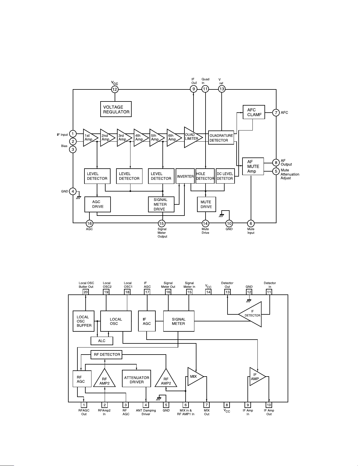
INTERNAL BLOCK DIAGRAM of Ics
■ IC101 DBL 1018(LA 1140)
■ IC201 DBL 1019 (LA1135)
Page 2
- 2-7 -
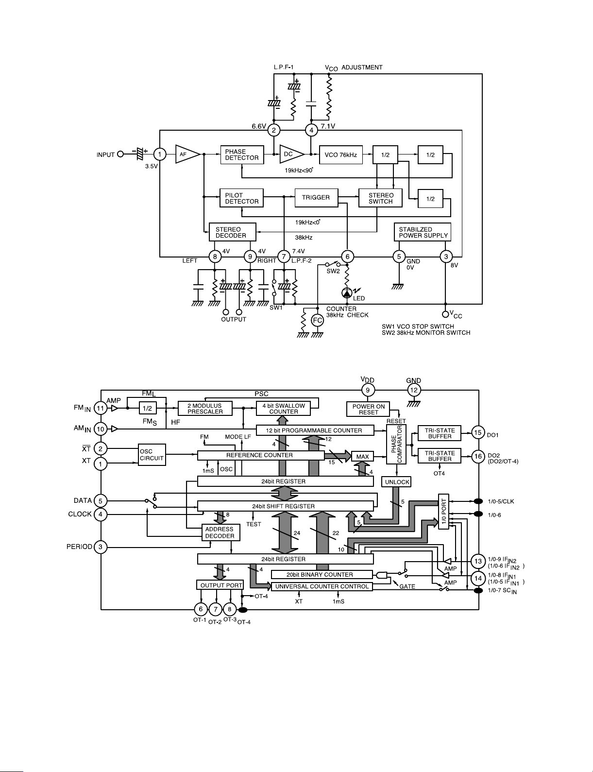
■ IC301 KIA6043S
NOTE: Mark terminals are not existence in KIC9256P, KIC9256F
Terminal name of KIC9256P, KIC9256F is shown in parentheses.
Others are common terminals.
■ IC401 KIC9256P
Page 3

- 2-8 -
■ IC402 µPD789104GS-204
PIN Port P-NAME I/O Act DESCRIPTION When not used REMARK
1 P23 FRTCLK O FRONT IC CLOCK Data OUTPUT
I DIODE MATRIX as DIO IN2 line
2 P24 ACC IN I ACC DETECT INPUT ACTIVE = LOW
3 P25 CDC DI I L CD CHANGER DATA INPUT
4 Avdd A/D Reference Voltage (5V)
5 P60 KEYIN I AD KEY - IN input.
Used for also front panel detecting.
Less than 0.17V : regarded as the panel opened.
Refer to application circuit.
6 P61 DIR I H/L TAPE DIRECTION INPUT (H = FORWARD)
7 P62 SD Tuner SEEK stop detector input
- Seek Stop threshold voltage :
AM : 1.2V, FM : 1.5V
8 P63 STIN I L FM Stereo detect input Active = Low
9 AVSS GROUND
10 NC NO CONNECTION
11 P50 CDCO O CDC Data Output : Should be connected to CDCI
12 P51 PEVDATA O E VR Communication DATA OUT
13 P52 MUTE/LED O Used as Power IC mute. Active = Low
Used as blinking LED. On duty = 10%
14 P53 TPMUTE I L TAPE MUTE INPUT (LOW = MUTE)
15 P00 FRTDO/ O FRONT IC DATA Out communication port
DIO IN0 I Diode matrix IN0 input
16 P01 CDON O H When CDC mode this port is high output
(future function)
17 P02 POWER O H When system is on, this port is used as power out
port
18 P03 TAPE IN I H For tape mode, Active high voltage should be applied.
L = RADIO mode.
19 RESET RESET INPUT
20 IC Connect to GROUND
21 NC NO CONNECTION
22 X2 X-tal
23 X1 X-tal
24 Vss System ground
25 Vdd System Power Supply (5V)
26 P10 FINH O L Front IC INH port.
27 P11 PERI/ O PLL IC PERIODE communication port
DIO OUT2 O Diode matrix DIO OUT 2 line
28 P20 PEVCLK O PLL IC and E. VOL IC CLOCK communication port
DIO OUT0 O Diode matrix DIO OUT 0 line
29 P21 PDATA O PLL IC DATA communication port
DIO OUT1 O Diode matrix DIO OUT 1 line
30 P22 FRTCE O FRONT IC CE communication port
DIO IN1 I Diode matrix DIO IN 1 line
Page 4

- 2-9 -
■ IC501 LA3160
■ IC601 PT2313L
Page 5

- 2-10 -
■ IC801 TDA8571J
■ IC901 LC75833E
 Loading...