

Page 1
DX-SR8 / T / E
Service Manual
CONTENTS
SPECIFICATIONS
General...............................................................................2
Transmitter........................................................................2
Receiver.............................................................................2
C IR C U IT D E S C R IP TIO N
1) Receiver System
2) Transmitter System.................................................5,6
3) Peripheral Circuits...................................................7,8
4) PLL Synthesizer Circuits...........................................8
5) R5F2L3ACANFP#U1 (XA1400 /XA 144 2 )
SEM IC O N D U C TO R DA TA
1) NJM4558M (XA0097)
2) BD1754HFN (XA1403)............................................ 11
3) NJM78M05DL1A (XA1118)
4) NJM7808FA (XA1106).............................................12
5) TC 4S66F (XA0115)..................................................12
6) BU4052BCF (XA 0236)............................................12
7) BU4001 BF (X A 0299 )
8) TA75S01F (XA0332)............................................... 12
9) LA4425A (XA0410 ) ..................................................12
10) TC74HC74AF (XA0459).......................................13
11) NJM3357M (XA0742)............................................13
12) NJM7805FA (XA0812 ) ......................................... 13
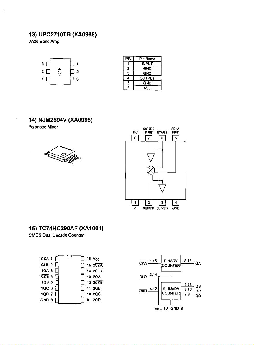
13) UPC2710TB (XA0968)......................................... 13
14) NJM2594V (XA 0995)............................................13
15) TC74HC390AF (XA1001).....................................13
16) MB15A01PFV1 (XA 1010)....................................14
17) LM2904PWR (XA1103)........................................14
18) LM2902PWR (XA1106)
19) S80845CLNB (XA1120)
20) TC4SU11F (XA1396)
21) TC74VHC393FT (XA 13 97)
22) XC9504B092AR (XA1398)
23) AD9833BRM A (X A1399)
24) R1EX24256ASAS0A#S0 (XA1401)
25) M61545AFP#DF0R (XA1402)
26) NJM 2068V (XA 1404)............................................16
27) Transistor, Diode and LED Outline Drawing.... 16
28) LCD Connection (EL0064 )
..................................................... 3,4
.....
9-11
.............................................. 11
...................................
..............................................12
........................................
......................................
............................................14
.................................
..................................
......................................15
..................
............................
..................................
11
14
14
15
15
15
16
17
EXP L O D E D V IE W
1) Front V iew
2) Main Side..............................................................20-22
PA RTS LIS T
FRONT Unit.....................................................................23
LCD Unit...........................................................................23
PA Unit........................................................................24,25
MAIN Unit..................................................................25-35
Mechanical Unit..............................................................35
Packing Unit....................................................................35
AD JU S T M E N T
1) Required Test Equipment.......................................36
2) Adjustment Spot........................................................37
3) PA Unit Adjustment...................................................38
4) MAIN Unit Adjustment.............................................38
5) RX Test Specification..............................................40
6) TX Test Specification............................................... 41
PC BO A R D VIEW
FRONT Unit Side A........................................................42
FRONT Unit Side B .......................................................43
MAIN Side A ....................................................................44
MAIN Side A No.1.......................................................... 45
MAIN Side A No.2 .......................................................... 46
MAIN S ide B ....................................................................47
MAIN Side B No .1.........................................................48
MAIN Side B No.2 .........................................................49
PA Side A .........................................................................50
SCH E M A TIC D IA G R A M
FRONT Unit.....................................................................51
MAIN Unit (MAIN C P U )
MAIN Unit (MAIN 1).......................................................53
MAIN Unit (MAIN 2 ).......................................................54
MAIN Unit (MAIN 3 ).......................................................55
MAIN Unit (PLL)
PA Unit (PA).....................................................................57
PA Unit (FILTER)............................................................58
B LO C K D IA G R A M .....................................................59
............................................................ 18,19
...............................................
...........................................................
52
56
A LIN CO , Inc
Page 2
N>
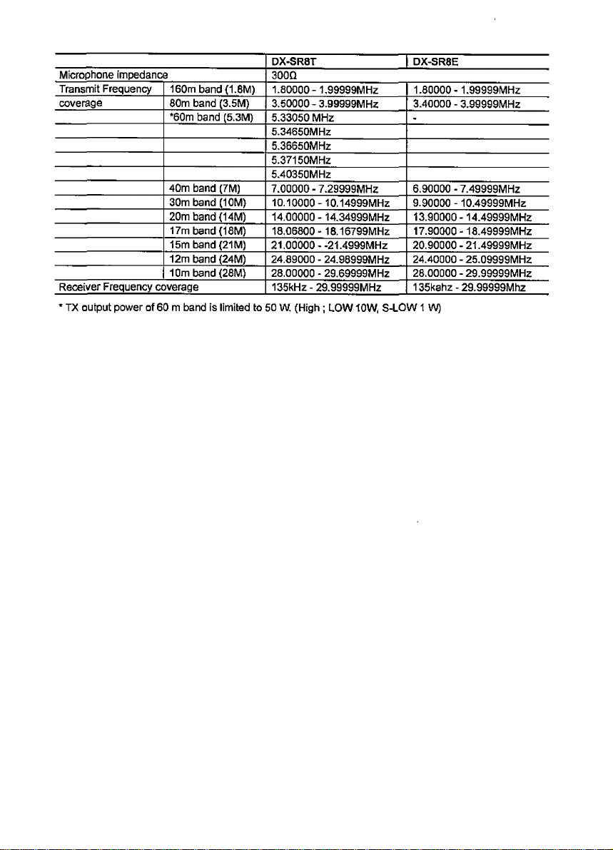
SPE CIFI CA TIONS
General
Operating mode J3E (USB, LSB),A3E (AM), A1A (CW), F3E (FM)
Number of memory channels 600 channels simplex
Antenna impedance
Frequency stability
Power requirement
Ground method
Current drain Receive 1.0A(max.) 0.7A (Squelched)
Operating temperature
Dimensions 240 (w) x 94 (h) x255 (d) mm (Projections not included)
Weight
Transmitter
Power output SSB, CW, FM
Modulation system
Spurious emissions Less than -50 dB (Less than -45dB in 30 m band)
Carrier suppression More than 40 dB
Unwanted sideband More than 50dB (1 kHz)
Maximum FM deviation
Receiver
Receiver type
Sensitivity SSB
Intermediate frequency
Selectivity
Spurious and image rejection ratio
Audio output power
RIT variable range
Transmit 20A
AM
SSB
AM
FM
CW
AM
FM (28 to 30 MHz) -6dBu (0.5uV)
SSB, CW, AM (narrow)
AM, FM
DX-SR8 ALL MODELS
500 unbalanced
±1ppm
13.8V DC±15%(11.7to 15.8V)
Negative ground
-10°C to 60°C (+14°F to +140°F)
(9.45" (w) x 3.7"(h) x 10”(d))
240 (w) x 100 (h) x 293 (d) mm
(9.45"(w) x 3.94" (h) x 11.54"(d))
Approx. 4.1kg (9 pounds)
100W (Hi) Approx. 10W (LOW) Approx.lW (S-LOW)
40W (Hi) Approw.4W (LOW) Approx.0.4W (S-LOW)
Balanced modulation
Lo power modulation
Reactance modulation
±2.5 kHz
Double conversion superheterodyne
{0.15 to 1.8 MHz) OdBu (1uV)
(1.8 to 30MHz) -12dBu (10uV)
(0.15 to 1. 8M Hz) +20dBu (1 OuV)
(1.8 to 30 MHz) +6dBu (2uV)
1** 71.75MHz 2nd 455kHz
2.4kHz/-6dB 4.5kHz /-60dB
6kHz/-6dB 18kHz/-60dB
More than 70dB
More than 2.QW (8Q, 10%THD)
±1.2 kHz
Microphone impedance 2kO
Transmit Frequency coverage
Receiver Frequency coverage
DX-SR8
1.6MHz-29.99999MHz
30kHz - 34.99999MHz
Page 3
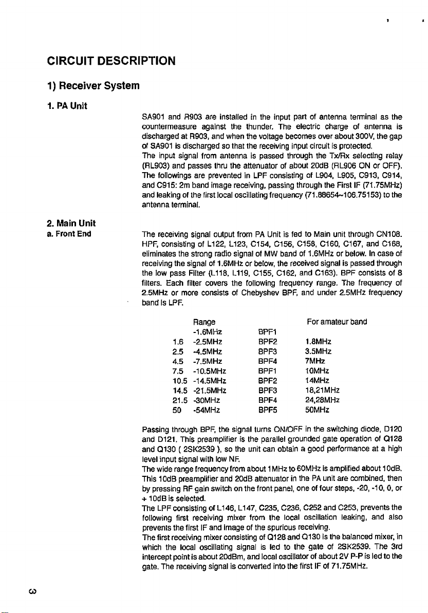
M icro p h o n e im pe d a n ce
Tr a n s m it F re q u en cy
covera g e
160m b a n d (1 .8M )
80m ban d (3 .5 M )
*60m band (5 .3 M )
300Q
1 .8 0 0 0 0- 1 .99 9 9 9M H z 1 .8 0 00 0 -1 .9 99 9 9 M H z
3.5 0 00 0 - 3.9 999 9 M H z
5.3 3 0 5 0 M H z
3.4 0 0 00 - 3.999 9 9M Hz
-
5.346 5 0M H z
5.3 6650 M H z
5.371 5 0M H z
5.403 5 0M H z
D X -S R 8 T | D X -S R 8 E
40m band (7M )
30m band (10 M )
20m band (1 4M )
17m band (18M )
15m b a n d (2 1M)
12m b a n d (2 4 M )
10m b a n d (2 8 M )
Rece iver F re q u ency coverage
7.0 0 00 0 - 7.2 999 9 M H z 6.9 0 00 0 - 7.49 9 9 9M H z
10 .1 00 0 0 - 10.1499 9 M H z 9 .9 0 0 0 0 -1 0 .4 99 99 M H z
14 .0 0 00 0 -1 4 .3 4 9 9 9 M H z 13 .9 0 0 0 0-1 4 .4 9 9 9 9M H z
1 8 .0 6 8 0 0 - 1 8 .1 6 7 99M H z 17 .9 00 0 0-1 8 .4 9 9 9 9M H z
2 1 .0 00 0 0--2 1 .4 9 9 9 M H z 2 0 .9 0 0 0 0-2 1 .4 9 99 9M H z
2 4 .8 90 0 0-2 4 .9 8 9 9 9 M H z
28.0 0 0 0 0 - 29.699 9 9M H z
13 5k H z -2 9.9 9 9 9 9 M H z
24.4 0 0 00 - 25 .0 9 999 M H z
28.0 0 0 00 - 29 .9 9 999 M H z
135kahz - 2 9.9 9999 M hz
* T X ou tput po w er of 6 0 m b and is limited to 50 W . (H ig h ; L O W 1 0W , S -L O W 1 W )
Page 4
CIRCU I T DE SCRIPT I ON
1) Receiver System
1. PA Unit
SA901 and R903 are installed in the input part of antenna terminal as the
countermeasure against the thunder. The electric charge of antenna is
discharged at R903, and when the voltage becomes over about 300V, the gap
of SA901 is discharged so that the receiving input circuit Is protected.
The input signal from antenna is passed through the Tx/Rx selecting relay
(RL903) and passes thru the attenuator of about 20dB (RL906 ON or OFF).
The followings are prevented in LPF consisting of L904, L905, C913, C914,
and C915: 2m band image receiving, passing through the First IF (71.75MHz)
and leaking of the first local oscillating frequency (71.88654-106.75153) to the
antenna terminal.
2. Main Unit
a. Front End
The receiving signal output from PA Unit is fed to Main unit through CN108.
HPF, consisting of L122, L123, C154, C156, C158, C160, 0167, and C168,
eliminates the strong radio signal of MW band of 1.6MHz or below. In case of
receiving the signal of 1.6MHz or below, the received signal is passed through
the low pass Filter (L118, L119, 0155, 0162, and 0163). BPF consists of 8
filters. Each filter covers the following frequency range. The frequency of
2.5MHz or more consists of Chebyshev BPF, and under 2.5MHz frequency
band Is LPF.
Range
-1.6MHz
-2.5MHz BPF2 1.8MHz
1.6
-4.5MHz BPF3
2.5
-7.5MHz BPF4
4.5
-10.5MHz
7.5
-14.5MHz BPF2
10.5
-21.5MHz BPF3
14.5
-30MHz BPF4
21.5
-54MHz BPF5
50
Passing through BPF, the signal turns ON/OFF in the switching diode, D120
and D121. This preamplifier is the parallel grounded gate operation of Q128
and Q130 ( 2SK2539 ), so the unit can obtain a good performance at a high
level input signal with low NF.
The wide range frequency from about 1 MHz to 60MHz is amplified about 10dB.
This 10dB preamplifier and 20dB attenuator in the PA unit are combined, then
by pressing RF gain switch on the front panel, one of four steps, -20, -10,0, or
+ lOdB is selected.
The LPF consisting of L146, L147, 0235, 0236, 0252 and 0253, prevents the
following first receiving mixer from the local oscillation leaking, and also
prevents the first IF and image of the spurious receiving.
The first receiving mixer consisting of Q128 and Q130 is the balanced mixer, in
which the local oscillating signal is led to the gate of 2SK2539. The 3rd
intercept point is about 20dBm, and local oscillator of about 2V P-P is led to the
gate. The receiving signal is converted into the first IF of 71.75MHz.
BPF1
BPF1
For amateur band
3.5MHz
7MHz
10MHz
14MHz
18,21 MHz
24,28MHz
50MHz
Page 5
b. The First IF Amplifier Circuit
XF102 and XF103 are the crystal filters of 71,75MHz. By the combination of
two filters, the unit has the characteristics of the band width of 15kHz or more
3dB and the value of guaranteed attenuation of 70dB or more. Here the image
ratio is determined 70dB or more (approx. 80dB). The first IF amplifier circuit of
Q124 located between the crystal filters to prevent the loss in the front-end and
mutual interference.
The first IF amplifier circuit Q124 decides the sensitivity after passing the mixer.
AGC voltage is applied to the second gate.
c. The Second Mixer Circuit, The Second Amplifier Circuit
DBM (Double Balanced Mixer) consists of L114, D111 and L115. The signal is
passed in the opposite direction while receiving or transmitting in this DBM.
Approximately OdBm is fed as the second local oscillating level, and the third
IP is approximately 10dBm.
The receiving signal (71,75MHz) and the second local oscillating frequency
(71,295MHz) is mixed, and unwanted signal is eliminated in LPF consisting of
L101, L102 and C119, then the signal of 455kHz is generated. After passing
through the switching diode D108, the signal is amplified in Q110. The source
of Q110 is controlled by the output of the noise blanker circuit.
d. IF Filter
After passing through the transmission/reception switching diode D110, the
signal Is led to one of three ceramic filters of 455kHz. The selectivity is decided
here except CW narrow.
SSB, AM-NARROW FL3(CFJ455K5) 2.4kHz/-6dB 4.5kHz/-6QdB
SSB-NARROW, CW FL2(CFJ455KB) 1.0kHz/-6dB 3.0kHz/-60dB
FM, AM FL4(CFW455G) 9kHz/-6dB 20kHz/-50dB
e. Second I.F.Amp
There are two switching diodes for input and output of each filter (D129 to
D150), securing isolation. The isolation required Is more than the guaranteed
attenuation for each filter (about 70dB). The filters not used are shorted by
diodes parallel to the filters and cut by the diodes in series, therefore the
combination achieves high level of isolation from the signal. The filter switching
is done by the Q141, Q142, Q143, Q145, D128, D145, D146 and D151, and
the switching configuration depends on the mode, Tx/Rx, and Wide/Narrow
status.
After the filter, passing thru a Tx/Rx switching diode (D128), the signal is
amplified by the Q138 and Q139, and buffered by the Q137. The second gates
of the Q110, Q138 and Q139 are controlled by the AGC circuit. The level of the
received signal for which AGC is applied Is of high amplitude and constant at
the output of the Q137.
This output is used for demodulation of SSB, AM, and CW modes besides used
for AGC detection. In the FM mode, the signal having amplified by the Q138 is
partly input to the IC110 (MC3357) thru the C353 and Is amplified and demodu
lated. The demodulated signal is amplified by an op-amp inside the IC110. A
feedback resistor (R351) has a parallel capacitor (C365) for de-emphasls. The
Q110, Q138 and Q139 are also operational during the FM mode and the AGC
is effected.
Page 6
f. Demodulator
When in SSB or CW mode, the local oscillation signal mentioned below from
DDS circuit Is Input to the balanced mixer of the IC104. The received signal is
input to pin No.5, the local signal at 5V p-p to pin No.7. The Q610 is amplifier
that amplifies the local signal to 5V p-p.
Local Osc: USB 456.5kHz + IF SHIFT
g. CW Audio Filter
The IC4 is an active filter combined of high pass and low pass filters by
op-amps, which has a passband of about 600Hz (-6dB) with its centre at about
800Hz.
h. AF Switchlng/AGC Time-Constant Switching
The IC107 is an analogue multiplexer with two channels and four contacts,
which switches the demodulated output and AGO time-constant dependent on
mode. The mode voltage is made by combination of the D139 and D140, which
is Input to pin No.9 and 10, thereby switching CW audio filter output and
demodulated output of (SSB), FM, and AM. While transmitting, 8V is imposed
to pin No.6 (inhibit) turning the demodulated output off.
I. AF Amplifier
The AF signal, after passing thru an analogue switch, is amplified by about
50dB with the IC113:A. The output of pin No.1 of the 1C113A is fed to AF Gain
potentiometer for audio output control. The potentiometer output is voltage-
divided with the R383 and R392 and is fed to the IC112, an AF amp. By said
voltage division, input level is adjusted at the same time the input impedance is
lowered for the IC112 therefore residue noise is lowered.
The 1C112 is an AF power amp, while the Q147 and C393 form ripple filter.
Over 2W output is obtained at 8 ohm load and 10% distortion. This output is
used as the terminal of packet RTTY, SSTV, etc.
]. AGC
The AGC is affecting to one stage in the first IF circuit, and three stages in the
second IF circuit, a total of four stages. Each amplifier stage is made of
3SK293 with AGC on the second gate. The bias on the first gate of 3SK293,
and the source resistor and voltage at the second gate have been determined
their operational level so that the gain Is lowered linearly against the voltage
lowering at the second gate. (The source resistor: 470 ohm; the first gate about
3.7). The D144 is for signal detection and the Q140 is for DC amplification. The
anode of the D135 Is set at 4.1V by the R321, D135, R280 and R292. Since
little current flows through the IC106C feedback resistor the VR104, input
resistor R290 and D135 to R321, the voltage of AGC line is about 4.2V. When
there is detection voltage on the D144 due to receiver input signal, the Q140
attempts to lower the AGC voltage. When AGC Is set FAST in SSB or CW,
there is the C336 between AGC line and the power supply. The raise in
receiver input signal is AGC controlled dependent on the time-constant which
is determined by R326 and C336 hence the transient response Is set.
Discharging is determined by the C336 and R290 and the resulting characteris
tic is of fast-attack/slow delay type.
LSB 453.5kHz + IF SHIFT
CWU 455.0kHz + (sidetone freq) + IF SHIFT
CWL 455.0kHz - (sidetone freq) + IF SHIFT
Page 7
k. S-meter, Squelch
I. Noise Blanker
When the AGC is set to SLOW, an analogue switch in the IC108 turns ON and
the R333 and C351 comes in parallel, and R333 with C351 makes discharge
time longer without affecting the attack time.When in AM mode, the C325 is
further added in parallel, which delays the attack time and the AGC response
becomes of average-value type. The D135 are for temperature compensation.
If the received signal delays with a narrow filter before AGC detection followed
by AGC-detectlon and amplification further delaying for AGC-detection, it
would cause amplifying with more gain and this loop would start hunting
effects. For anti-hunting purpose in this regard, the AGC has more OR
time-constant and slower operation as applicable stage comes closer to the
antenna input. The final stage of I.F. varies its amplification immediately by the
AGC detection voltage resulting in uniform level received signal, dependent on
the transient response. That is, if the received signal suddenly increases, the
received output would first be controlled for uniform output by the I.F. final
stage, then step by step the AGC is applied to earlier stages, finally affecting
the AGC on the final stage to be smaller. For AM reception, there is already
AGC voltage due to carrier, and the AGC is averaged independent of the
modulation level.
TThe output of IC106C Is sent to the CPU to display the S-meter. The output
signal of IC106C is fed to pin IC106D. The voltage of pin No. 13 of IC106D is
determined by the squelch VR of front unit. Comparing with this voltage, the
squelch is opened or closed. During the check operation the CPU output
decreases the voltage of squelch VR in front side to open the squelch deliber
ately. The squelch output controls the IC106C, at the same time it is provided
to the front unit to light RX LED.
This circuit eliminates the pulse noise of a car, etc. Because the noise emitting
time is short, in this duration the operation of receiver is stopped to prevent the
unit from emitting a noise. The pulse noise is delayed when it is passed through
the narrow band filter, and the emitting time becomes longer. It makes difficult
to eliminate the noise, so it is necessary to eliminate the noise in the earlier
stage. A part of the second mixer output, whose band width is limited, is
amplified in Q118, Q114, Q115, and Q116. The signal is detected in D115 and
D118, and the AGC voltage is applied to Q115, Q114 and Q116.
The charge time constant of this AGC is determined by R192 and C201, and
also the discharge constant is determined by R191+R192, C201. The voltage
of AGC does not rise suddenly because of the charge constant, so that this
voltage is not applied to almost all the short signals such as pulse noise, but is
applied to the continuous signals such as receiving signal and amplifier gain is
decreased.nal.
Page 8
2) Transmitter
1. MAIN Unit
a. Mic Amp
b. Balanced Mixer
The input signal from microphone goes thru mic-gain pot the VR117 and is fed
to a low noise amp the Q180. At the mic terminal there is an 5 V bias thru the
R109 for providing voltage to certain type of mics. The IC119A has the gain
(about 20dB) which is determined by the R492 and R512. When in FM mode,
the gain increases by about 35dB due to the R494 parallel to the R512 thru the
Q175, and by the C465 the lower cut-off frequency is Increased thereby
activating pre-emphasis and limiter. When in SSB or AM, if the speech
compressor is turned ON, the gain increases by about 35dB due to the C460,
R487, and Q172, and the IC119:A works as a limiter. The C460 cuts off lower
spectrum portion and the audio quality becomes suitable for speech compres
sion. The in FM, the gain is adequately obtained and there is no effect of
speech compression. If the FM sub-tone is activated, the output of the 1C119:A
pin No.1 is voltage divided by the R499 and R509, and the sub-tone fed thru
the R509. The IC119:B Is a low pass filter which works as a splatter filter when
in FM and a low pass filter when speech compressor is in use. The output is
either fed to PLL circuit for FM modulating, or to the 10105 for balanced
modulation. The output of the 10105 is muted by the Q178 when in CW or FM.
IC105 Is the balanced mixer, and the carrier is suppressed in SSB mode. To get
more ratio or carrier suppression, the balance adjustment of VR102 and
VR103 are applied. The carrier is necessary in CW/FM/AM mode, so the input
of Pln7 is made unbalanced by applying the DC voltage to obtain the carrier. By
applying the DC in AM/FM mode, or by keying in CW mode, the balance Is
broken to obtain the carrier wave. VR115 is used for the adjustment or carrier
level in AM/FM mode. VR118 is used for the adjustment of carrier level in CW
mode. In the AM mode, the DC and modulation is added simultaneously. In
SSB mode, the modulation Is added by R488. In AM mode, D174 Is DC-biased
and turned ON. Then the attenuator consisting of R488 and R443 or R523
limits the modulation.
c. IF filter
d. IF Amp, Second Mixer
The output of the 1C105 goes thru a temperature compensating thermistor
TH101 and the D128 and is fed to bandwidth limiting I.F. filter. Pulling up
cathode of the D128 when in Tx (and L when in Rx) makes Tx/Rx isolation
better. When in SSB mode, the signal becomes DSB without the carrier.
Switching of the filters is done by the diode switching mentioned before. For
each respective mode, filters are used as follows.
SSB, CW, AM-NARROW FL102 (CFJ455K5) 2.4KHz/-6dB 4.5KHz/-60dB
CW-NARROW FL101 (CFJ455K8) 1.0KHz/-6dB 3.0KHz/-60dB
FM, AM FL103 (CFW455G) 9.0KHz/-6dB 20KHz/-50dB
Having passed the filter, the signal passes thru a switching diode (D110), amp
(Q104), and the D108, and thru the second mixer in reverse direction of Rx,
making 71.75 MHz signal. The Q107 depends on CW keying that improves
isolation when CW key is up. An ALC voltage is applied on the second gate of
the Q104. Signals from 71.295MHz local oscillator and reverse heterodyne are
filtered by the XF102. The signal is amplified by the Q614 and is input to a
balanced mixer. (D111).
Page 9
e. Transmitter First Mixer
f. Tx Pre AMP
g. CW Keying Circuit
The first transmit mixer comprising of the Q103, Q108, L104 and L117 is a
balanced type mixer and Input about 3dBm of local oscillator
(71.75MHz+TxFreq) to obtain the wanted frequency. The signal converted to
the wanted frequency by the first Tx mixer Is passed thru an LPF to filter out the
local frequency and image components before it Is Input to the Tx preamp.
The Q105 Is a wide band amplifier. It can put out high power with saturating
output of about + 13dBm and more than 20dB gain. Inserting attenuators on
both the input and output make It widen Its range with more stability, The output
at the Transmitter First Mixer Is about OdBm when the transmitter power is
100W.
By keying, the Q165 is turned on to the base of the Q162 in the main unit is
pulled to Low which causes the collector to output a voltage. This output
controls all the circuit which operates by CW keying. The output of the Q162
collector goes thru the D180, IC105, VR103, and D126 and by applying a DC
voltage to the balanced mixer it unbalances the mixer and generates a carrier.
VR118 determines the CW waveform of rising edges and falling edges by
adjusting the carrier level in R525 and C488. At the same time, the Q159 is
turned ON to turn OFF the Q107 isolating in keying. The C428 makes the Q107
OFF duration longer than keying duration to avoid effects to the output
waveform. By the D180 a voltage is input to pin No.10 of the 1C119:C, and by
the output from pin N0.8 the Q161 is turned ON and the D171 pulling the PTT
line down to Low brings the transmitter ON. The capacitors at the input of pin
No.10 of the 10119:0 (C246, C247) determines transmit time delay after stop
of keying. The BK1, BK2, and BK3 are 3 bit break-in time constant voltages
which are combined by the combination of the R469, R470 and R471 as D/A
for obtaining 8 levels of voltage. When all of the BK1, BK2, and BK3 are low,
the status if full-break-in, when more than one of the BK1, BK2, and BK3 have
voltage the status is semi-break-in and the break-in time fastest when all of
them have voltage. When in full-break-in, each of the BK1, BK2, and BK3,
voltages are low hence the Q164 is OFF, making a very fast discharge
time-constant with the 0431 alone. When either of several of the BK1, BK2, or
BK3 has voltage, the Q164 would turn ON and the C434 would be added
parallel to the C431 making the time-constant longer which determines the
delay time for semi-break-in. There are 7 levels of semi-break-in voltages out
of the BK1, BK2, and BK3, that Is fed to the IC119:C as comparative voltage to
change the discharge time constant. Thus the time constant is the shortest if all
of the BK1, BK2 ,BK3 outputs voltage. When In AUTO-break-in, the output is
from BK1 only, and the comparative voltage for the IC119:C is controlled with
the output voltage of the IC119:D, The keying output when in AUTO mode is
output with each keying using the one-shot multi-vibrator comprising of the
IC120:A and B. Hence the average value of the IC120:A output voltage would
be proportional to average speed of keying. To obtain average voltage, the
R463 and C432, etc. are used for Integrating, and the output is DC amplified by
the IC119:D whose output is used as comparative voltage for keying. The D182
is for turning OFF when in AUTO mode; when AUTO is low, the voltage
charging the C432 is shorted and AUTO is stopped.
Page 10
o>
The D179 and R457 help to follow speeding up the keying, while the D176 and
R458 determine the discharging time constant In transmission and elongate
the time constant in reception so that it compensates the time constant
recovery during the reception. By doing this, the circuit can follow the keying
speed; transmission can continue between letters; and reception can take
place between words. The circuit is good typically between 30 characters per
minute to 200 characters per minute.
h. Power Control/ALC Circuit
The forward voltage obtained in the PA unit correspondent with transmit power
is input to the IC118:A for invert amplification. At the non-inverting input there is
a voltage, and the output voltage is shifted by the non-inverted input voltage.
There is already about 4.0V on the ALC line which is applied to the second gate
of amplification stage that is under ALC control. When a forward voltage is
applied, the output voltage of the 1C118:A goes down, and when becomes
lower than about 3V, the D160 lowers the voltage of the ALC line. The VR112
is for adjusting the Tx output to 100W (High power). The VR119 is for adjusting
the Tx output to 10W (Low power). The VR120 Is for adjusting the Tx output to
1W (super Low power). By I is soldering, Q166 turns ON and by having the
VR114 in parallel the voltage is brought down to result in SOW. When in AM, the
R448 comes in parallel to lower the output to 40W. When in Low power, the
LOW line brings the R528 and VR119 in parallel to lower the voltage. When in
super Low power, the slow line brings the R529 and VR120 in parallel to lower
the voltage. The Q158 and VR113 are for making the (antenna matcher) TUNE
output to 10W output. Necessary output, however, may be different depending
on the automatic tuner. When the SWR Is high, reflected voltage turns on the
Q158 lowering the power. The Q158 is activated from SWR 3 approximately.
I. Overcurrent Protection
The voltage difference detected in the PA unit by the final collector current us
differentially amplified by the IC118:B. The output voltage lowers as current
increases and at some point the ALC line is pulled down thru the D160 lowering
the output power. The operating point is determined by the VR110.
j. RF meter circuit, ALC Indication
The forward voltage Is amplified by the 1C118:D for driving the meter. The
D164, R433 and C419 are for instant peak-holding to show the meter more
visible. The D163 and D136 switch to S-meter. The ALC voltage is invert
amplified by the IC118:C. The output voltage is divided from 8V thereby
lowering the feedback resistance so that tolerance caused by bias-leakage is
minimized; further this feedback resistor lets some current to the R423 to
obtain 4.0V to the ALC line. The output Is fed to the base of the Q150, leading
to the front unit tell the CPU to switch Tx and Rx besides illuminating the Tx
LED.
I
Page 11
2. PA Unit
a. Power Amp
The signal input is amplified by the Q803 to about 100mW. By having the idling
current of about 100mA the amplification is A-class. With the feedback the
frequency response is compensated, and with a capacitor parallel to the
emitter resistor the frequency is compensated totally. Then the signal is
amplified to about 5 watt with the Q801 and Q805 (RD16HHF1) where the
idling current is 800mA (adjusted with the VR804) in push-pull configuration.
The D804 and D805 is thermally contacting the Q801 and Q805 to compensate
Idling temperature.
b. Final Power Amp
c. Cooling Fan Control
d. Protection Circuit
There is about 1.6A of Idling current in the final amp circuit consisting of the
Q802 and Q804 (RD100HHF1). The D801 and D802 are thermally conducting
with the Q802 and Q804 for temperature compensation. Feedbacks exist thru
the R804 and R822 from collector side averaging the gain in a wide range. The
output of 100W goes to the filter circuit. The collector current of the Q802/Q804
is detected due to the voltage drop caused by resistance of the FB803 and
L801, and is output to the main unit.
The fan is controlled under the temperature of the Q802 and Q804 which is
sensed by a thermistor (TH801). While transmitting, due to temperature rise,
the resistance of the TH801 goes down and voltage of inverted input for the Pin
No.1 of IC101 (MAIN UNIT) goes down. The IC101 (Pin No.1) input is applied
a voltage corresponding to its voltage thus Is compared. When the temperature
is over 50 degrees Celsius approximately, the inverted-input voltage would go
down with comparative voltage, and by the comparator output voltage of the
Pin No.74 of IC101, the Q183 is turned ON and the fan starts running.
As a protection for the final power amp, power down circuits detecting SWR
excessive current, and temperature rise have been installed.
Page 12
3) Peri pheral Circui ts
1. Beep and Sidetone Circuit
Sidetone is output by the STON line at pin No.24 of the CPU (MAIM UNIT) in
square wave. Beep Is output by the beep line at pin No.16 of the CPU (MAIN
UNIT) in square wave. The sidetone frequency is swltchable in the range of
400Hz to 1kHz. The VR1 is the volume control put which leads to the AP amp.
2. Tune Circuit
At the start of the tuning, the TUNE voltage comes out by which the one-shot
multi-vibrator operates and by the Q168 approximately 8V is output to
command the external auto tuner as a starting signal. Separately, an output
which goes low while tuning is created by the Q169 using the TUNE voltage.
When the starting signal is received by the external auto tuner (e.g. EDX-2),
the tuner outputs the said (low) output at TKEY terminal, The radio’s CPU
monitors the TKEY terminal and while the voltage Is at low level the radio is put
to the TUNE mode. If the TKEY terminal is low for more than 20 seconds, the
CPU releases the TUNE mode. During the TUNE mode the radio transmits in
AM mode besides microphone Is muted and the carrier is suppressed at 10W
(adjustable).
3. Regulated Power Supply
The 1C115 Is a regulated power supply of 8V output. The voltage necessary for
transmission, namely T8V is created by the Q149, and for reception R8V by the
Q152. The IC117, Q151 and Q155 are Tx/Rx control. When PTT line is
grounded at the output of the Q161 by mic’s PTT or CW keying, a High level is
output from the IC117:C, and buffered by the Q150 the output is sent to the
CPU in the front unit for Tx/Rx switching. The IC117:C, having delayed the
rising of reception with the R413, C408, and D158, controls Q149 with Q151.
When transmitting, the current flows from 13.8V thru the R410 and D156, and
since the Q149's base voltage is higher by one diode difference than 8V, the
emitter output will be just 8V. When transmitting, the Q151 is turned ON thus
the Q149’s base voltage will be OV, resulting no output on T8V line. When
receiving, the T8V line is shorted by the D157 to discharge remaining charges
in the capacitors on T8V line. The Q152 while receiving, similarly as T8V line,
has currents coming thru the D167 and R432 from the 13.8V line, and since the
base voltage of the Q152 is higher by one diode voltage than 8V, the base
voltage of the Q152 will be 0V hence no output on R8V line. When transmitting,
the R8V line is shorted by the D168 to discharge remaining charges in the
capacitors on R8V line. The Input to the IC117:D, which goes low when
reception Is started, Is delayed with the R421 and C412, then inverted by the
IC117:B, followed by the Q155 to control R8V. if a voltage is applied to pin No.8
of IC117:C, the output at pin No. 10 would vary with PTT going Low, hence a
PTT Lock is activated.
4. Mode Voltage Functions Control, BPF/LPF Switching
The CPU (MAIN UNIT) is controlling the mode voltage, preamp On/Off, Attenu
ator, Power, BPF/LPF switching, AGC, break-in, and PTT-Lock. For each
mode, the Q167, Q170, Q171, Q177, Q179, Q181 and Q182 are turned on
providing 8V.
Page 13
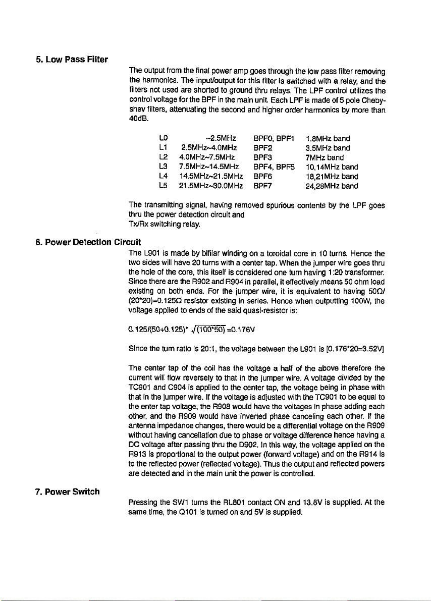
5. Low Pass Fi lt er
The output from the final power amp goes through the low pass filter removing
the harmonics. The input/output for this filter is switched with a relay, and the
filters not used are shorted to ground thru relays. The LPF control utilizes the
control voltage for the BPF in the main unit. Each LPF is made of 5 pole Cheby-
shev filters, attenuating the second and higher order harmonics by more than
40dB.
The transmitting signal, having removed spurious contents by the LPF goes
thru the power detection circuit and
Tx/Rx switching relay.
6. Power Detection Circuit
The L901 is made by bifilar winding on a toroidal core in 10 turns. Hence the
two sides will have 20 turns with a center tap. When the jumper wire goes thru
the hole of the core, this itself is considered one turn having 1:20 transformer.
Since there are the R902 and R904 in parallel, it effectively means 50 ohm load
existing on both ends. For the jumper wire, it is equivalent to having 500/
(20*20)=0.125Q resistor existing in series. Hence when outputting 100W, the
voltage applied to ends of the said quasi-resistor is:
0.125/(50+0.125)* VO00*50) =0.176V
Since the turn ratio is 20:1, the voltage between the L901 is [0.176*20=3.52V]
The center tap of the coil has the voltage a half of the above therefore the
current will flow reversely to that in the jumper wire. A voltage divided by the
TC901 and C904 is applied to the center tap, the voltage being in phase with
that in the jumper wire. If the voltage is adjusted with the TC901 to be equal to
the enter tap voltage, the R908 would have the voltages in phase adding each
other, and the R909 would have inverted phase canceling each other. If the
antenna impedance changes, there would be a differential voltage on the R909
without having cancellation due to phase or voltage difference hence having a
DC voltage after passing thru the D902. In this way, the voltage applied on the
R913 is proportional to the output power (forward voltage) and on the R914 is
to the reflected power (reflected voltage). Thus the output and reflected powers
are detected and in the main unit the power is controlled.
LO
L1
L2
L3 7.5MHz~14.5MHz
L4
L5
-2.5MHz
2.5MHz~4.0MHz
4.0MHz~7.5MHz
14.5MHz~21.5MHz BPF6
21.5MHz~30.0MHz BPF7
BPFO, BPF1 1.8MHz band
BPF2 3.5MHz band
BPF3
BPF4, BPF5
7MHz band
10,14MHz band
18,21 MHz band
24,28MHz band
7. Power Switch
Pressing the SW1 turns the RL801 contact ON and 13.8V is supplied. At the
same time, the Q101 is turned on and 5V is supplied.
Page 14
0 0
8. Power Suppl y and Resett ing
9. Dimmer
10. LCD
11. Tone
12. Electronic Keye
The IC102, resetting IC for resetting the CPU, turns on and off at 4.5V. When
OFF (OV) the CPU resets. Then the IC1004’s reset signal goes Low and the
CPU stops. The IC116 is the power supply for the CPU, which is made
separate in order for the voltage to sustain 5V until the data is written to the
EEPROM and resetting signal is input.
A regulated power supply of 8V Is made of the IC115. The voltage of 8V Is
supplied to D3, D4, D5 and D6. The CPU’s EN output Is a pulse, which current
value from D3 to D6 is set. When the illumination is at the highest intensity, the
EN output is constant at 5V.
The CPU turns ON the LCD via segment and common terminals with 1/4 the
duty and 1/3 the bias, at the frame frequency of 125Hz.
The CPU (IC101) is equipped with an internal tone encoder. The tone signal
(67.0 to 250.3Hz) is output from pin 45 of CPU. The output of the CPU leading
to the mic amp LPF having mixed with audio signal. The tone is output only
when in FM mode.
The CPU (IC101) is activated by input to pin No.68 for dots, and pin No.69 for
dash. When ElecKey is ON, the electronic keyer in ON, and when Eleckey is
OFF the keying is of semi-automatic (the "bug key”) operation.
13. Cloning
14. Miscellaneous
The pin 58 of CPU is clone data transmission, and the pin 57 of CPU is
receiving data. Each data is of one line, and input/output is done thru JK2 on
the front unit.
The X1 is a ceramic resonator of 8MHz carefully chosen on its harmonics not
interfering on amateur bands. For the front panel switches, the Y0, Y1, Y2 and
Y3 with regard to the DB0~DB5 are monitored to determine which key is
pressed. On the terminals of RIT and IF-Shift pots, 5V is applied and the
voltage at the input of A/D determines the positions of these pots. The Q1 is for
transmit detection whose output from the main unit and illuminating the Tx
LED. For this reason it cannot be directly Input to the CPU therefore the change
is only either on or off. The 02 is the squelch output from the main unit which
illuminates the Rx LED.
I
Page 15
4) PLL Synt hesizer ci rcui ts
1. Reference frequency oscillator circuit
The reference oscillation frequency for the PLL of the second local oscillator
reference and DDS clock, etc. is set at 16.777216M Hz. The signal is oscillated
by the X601, Q609, and Q611 buffered with the Q608. It is used for the DDS
clock for BFO oscillation. It is further divided 1/2064 with the IC606 to
8.128496KHZ for the second local oscillator PLL (IC606) reference frequency.
2. First Local Oscillator i
The Q605 is a Hartley oscillator with the Q605 gate grounded which works as
VCO with the oscillation frequency range of 71.75 to 106.75MHz. The Q601
eliminates ripples for stabilizing the power supply, while the Q604 is a buffer
circuit. The output is divided 1/8 with the IC610 and divided 1/5 with the IC611,
hence 1/4 of the first local oscillator frequency (about 1.8 to 2.5MHz) is input to
the phase comparator IC607. Meanwhile the DDS in the IC603 can output in
0.25Hz step, and with a D/A converter of 10bit and LPF, a sinusoidal wave that
is i 1/40 of the first local frequency can be obtained. This output, with the phase
comparator will control the signal. The oscillator output frequency will be 10Hz
patch (0.25*40), The IC607 output goes thru a loop filter which is made of high
response, low noise op-amp inside the IC601A: controlling the D602, the
oscillation frequency is controlled. To widen the lock range, some voltages are
supplied to cathodes of the D602. The locking voltage applicable to the anode
of; the D602 is in a wide range of 2V to +6V. The IC602 and the Q603 are the
necessary negative voltage, and about -6.5V is attained.
3. Second Local Oscillator
The reference oscillation frequency input to the IC606 is 8.388608MHz which
is divided 1/2064 inside, and the comparison frequency is about 8.128496KHz.
The Q615 is a VCO with 71.295 MHz which is buffered with Q616. The output
is'amplified by the amplifier Q620, and dividing it 1/8771 in the IC606, it is fed
to.a phase comparator and thru a loop fitter, the oscillation frequency is output,
controlled by the D605. Also, this output is amplified by the amplifier Q614 and
fed to the second mixer circuit. When transmitting FM, the anode of the D605
will be superimposed by the modulating signal from the microphone, modulat
ing into FM signal. When in FM mode, the C697 is added to a loop filter by the
Q618, having the time constant larger and the control under the modulation is
unable, a modulated signal is created thru the VCO. The IC605 is an analog
switch which enables frequency modulation on the VCO only when in FM
mode.
4 .1.F. Shifting (AIF)
When in SSB or CW, by varying the first local and BFO interlocked, it is
possible to change the relative receiving bandwidth without changing the
receiving frequency. The range for the I.F. shifting for DX-SR8 is +/-1.5kHz in
50Hz pitch.
Page 16
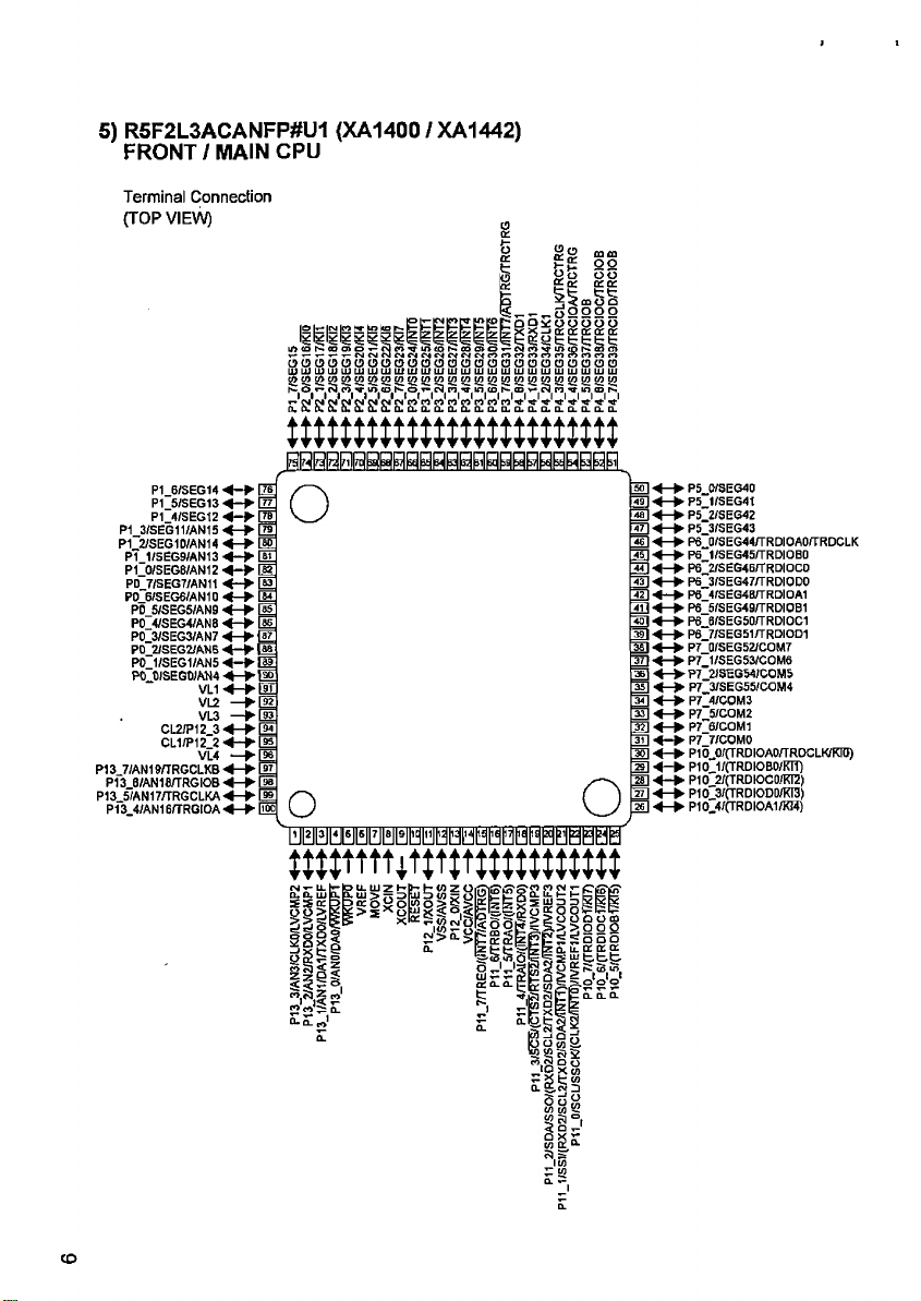
5) R5F2L3ACANFP#U1 (XA14 00/XA1442)
FRONT / MAIN CPU
Terminal Connection
(TOP VIEW) 0
U)0SCOOtOi-N(O^iB(ONOO>O«-NcOyiAlD
0 0 0 0 0 0 0 0 0 0 ( 5 ( 5 0 0 0 0 0 0 0 0 0 0
LU LU LU LU LU LU LLJ LU LLf LLt LLf LLf 111 LU LU LU LU LU LLI LLI LLI LLI
I-'-,©. c5. CO,^¡r>5 , o. ^ S. cq ¡n. 3 £ o. S F5,5
^ £* £* S4 £* £* S1 £* & S? 5? K? 5? 5? £? rt rt '* '* '* '* '*
CWO-OLO.a-a.Q.£LtLtLlLtLlLdLlLlLIL[LILILQ.Q.Q.Q.Q.
mnmmtmmmn
<d ca
go
HP OO
oo
q: a:
i s . s
222
ooo
czcccc
t t t
hi hi in
in to to
in (o,
I
t
P1_S/SEG14
P1_5/SEG13
P1_4/SEG12
P1 3/SEG11/AN15
P1~2/SEG10/AN14
P1JI/SEG9/AN13
P1_0/SEG8/AN12
PD 7/SEG7/AN11
PD_B/S EG6/A N10
P0_5/SEG5/AN9
PO 4/SEG4/AN8
PO 3/SEG3/AN7
PQ_2/SEG2/AN5
P0_1/SEG1/AN5
PO 0/SEGWAN4
P13 7/AN19/TRGCLKB
P13 6/AN18/TRGIOB
P13 5/AN17/TRGCLKA
P13_4/AN 16/TRGlOA
VL1
VL2
VL3
CL2/P12 3
CL1/P12 2
VL4
DIQIBIDIBIBIQIBISllEIIIEIEISEiiilEIEISiaiSISIS
«titttnnnt nnwi tt tt
t. o S o
Q O
t-*9 5 «
Q.£,S3
P5 0/SEG4Q
P5_1/SEG41
P5~2/SEG42
P5~3/SEG43
P6-0/S EG44/TR Dl 0 AO/TR DCLK
P6 1/SEG45/TRDIOBO
P6~2/S EG4 6/TR Dl OCQ
P6~3/S EG47/T RDI0 DO
P6_4/S EG4 8/TRDIO A1
P6_S/S EG4 9/TRDI OB 1
P6 0/SEG5O/TRDIOC1
P6_7/S EG 51 /T RDIOD1
P7_0/S EG 52/CO M7
P7 1/SEG 53/CO M6
P7~2iScG54JCOM5
P7~3/SEG55/COM4
P7~4/COM3
P7- 5/COM2
P7_6fCOM1
P7_7/COMO
P10 0/(TRD IOAO/TRDC LK/KTO)
P10_1/(TRDIOBO/KTT)
P10_2/(TRD IOCO/KI2)
P10_3/(TR DI0DD/KI3)
P10 4/(TRDIOA1/K!4)
5%
CD
Page 17
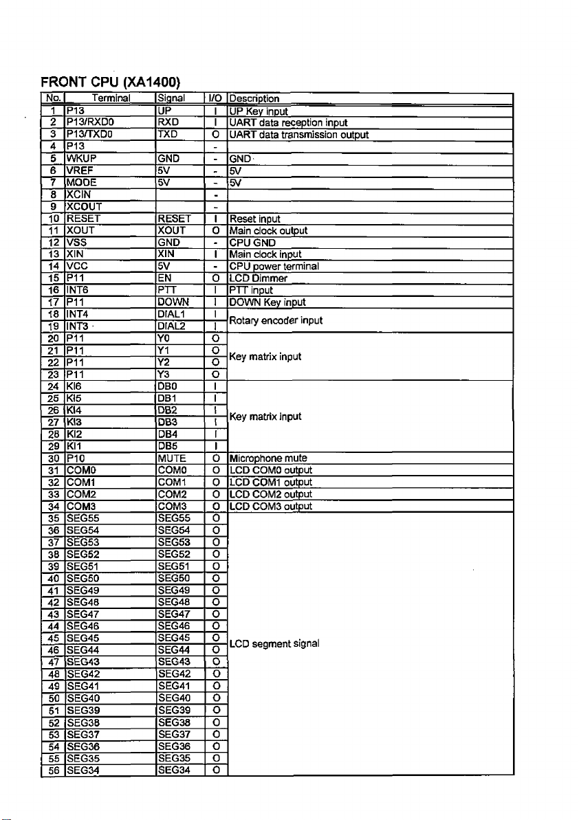
FRONT CPU ( XA1400)
No.
2
3
4 P13 -
5
6
7 MODE
8 XCIN
9
10 RESET
11
12
13 XIN
14 VCC
15 P11
16 INT6
17 P11
18 INT4
19
20 P11
21 P11
22 P11
23 P11
24 KI6
25 Kl 5
26 KI4
27
28 KI2
29
30 P10
31
32 COM1
33 COM2
34 COM3
35 SEG55
36 SEG54
37 SEG53
38 SEG52
39 SEG51
40
41
42
43 SEG47
44 SEG46
45 SEG45
46 SEG44
47 SEG43
48
49
50 SEG40
51
52 SEG38
53 SEG37
54 SEG36
55 SEG35
56 SEG34
Terminal
1 P13
P13/RXD0
P13/TXD0
WKUP
VREF
XCOUT
XOUT
VSS
INT3
K13 DB3
KI1
COMO
SEG50
SEG49
SEG48
SEG42
SEG41
SEG39
Signal I/O Description
UP
RXD
TXD
GND
5V
5V -
RESET I
XOUT 0
GND
XIN
5V
EN
PTT I
DOWN I DOWN Key input
DIAL1 I
DIAL2
Y0 O
Y1
Y2
Y3
DB0 I
DB1 I
DB2 I
DB4 I
DB5
MUTE 0
COMO 0 LCD COMO output
COM1
COM2 0
COM3 0 LCD COM3 output
SEG55 0
SEG54
SEG53
SEG52 0
SEG51 0
SEG50
SEG49 0
SEG48
SEG47 0
SEG46
SEG45
SEG44 0
SEG43 0
SEG42 o
SEG41 0
SEG40 0
SEG39 0
SEG38 0
SEG37 0
SEG36 0
SEG35 0
SEG34 0
I
UP Kev inDUt
I
UART data reception input
0
UART data transmission output
-
GND
-
5V
5V
-
-
Reset input
Main clock output
-
CPU GND
I Main clock input
-
CPU power terminal
LCD Dimmer
0
PTT input
Rotary encoder input
I
0
Key matrix input
0
0
Key matrix input
l
I
Microphone mute
LCD COM1 output
0
LCD COM2 output
0
0
0
0
0
0
LCD segment signal
Page 18
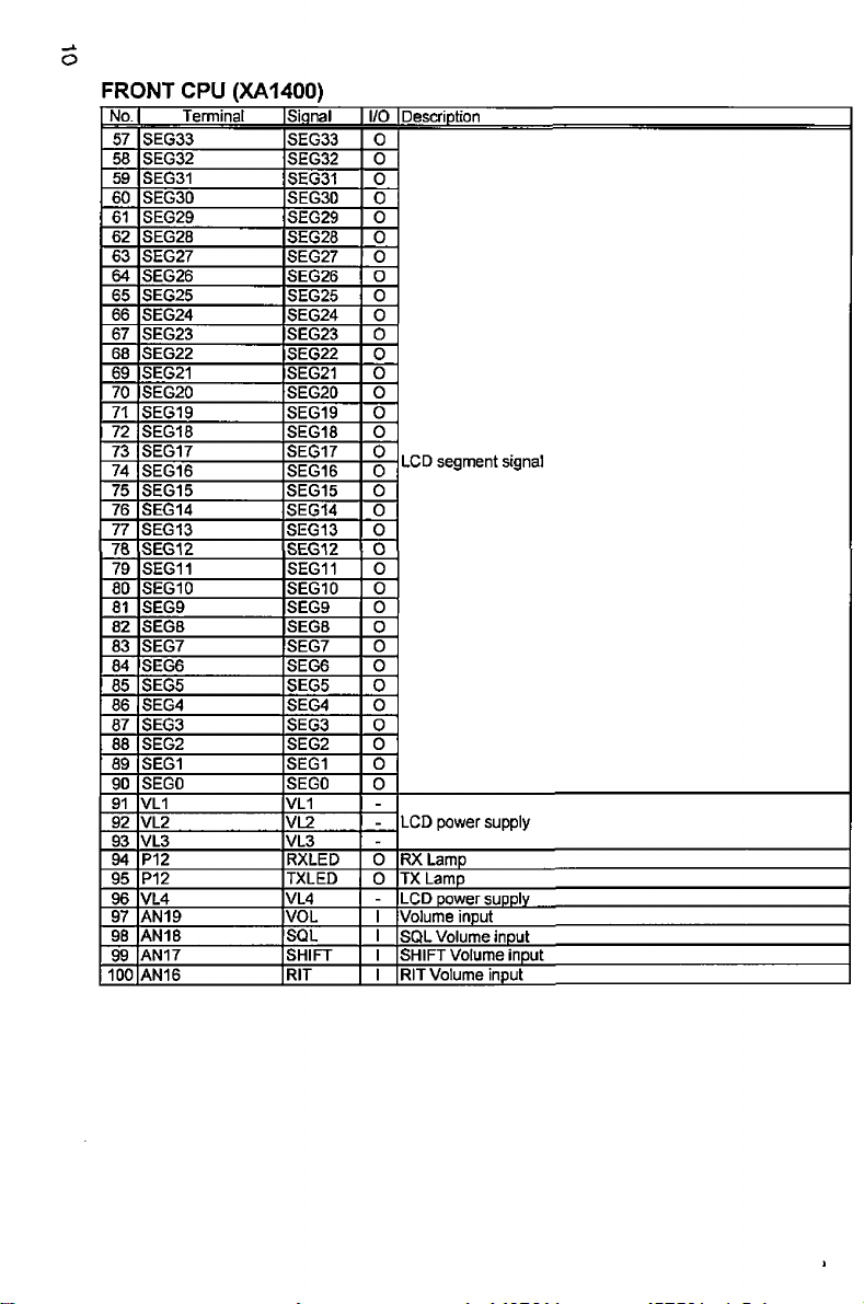
FRONT CPU (XA1400)
No.
57
58
59 SEG31
60 SEG30
61
62 SEG28
63 SEG27
Terminal Signal I/O Description
SEG33 SEG33 O
SEG32
SEG32 O
SEG31 O
SEG29
SEG30
SEG29 O
O
SEG28 O
SEG27 O
64 SEG26 SEG26 0
65 SEG25 SEG25 O
66 SEG24
SEG24 O
67 SEG23 SEG23 O
68 SEG22
SEG22 O
69 SEG21 SEG21 0
70 SEG20 SEG20 0
71 SEG19 SEG19 0
72
SEG18 SEG18 0
73 SEG17 SEG17
74 SEG16 SEG16
O
LCD segment signal
O
75 SEG15 SEG15 O
76 SEG14
77
SEG13 SEG13 O
SEG14 O
78 SEG12 SEG12 0
79 SEG11 SEG11 O
80 SEG10 SEG10 O
81 SEG9 SEG9 0
82 SEG8 SEG8
0
83 SEG7 SEG7 0
84 SEG6 SEG6 0
85 SEG5 SEG5 0
86 SEG4 SEG4 0
87
SEG3 SEG3 0
88 SEG2 SEG2 0
89 SEG1 SEG1 0
90 SEGO SEGO
91 VL1 VL1
92 VL2 VL2
93 VL3 VL3
0
-
-
LCD power supply
-
94 P12 RXLED 0 RX Lamp
P12 TXLED
95
96 VL4 VL4
TX Lamp
0
-
LCD power supply
97 AN19 VOL I Volume input
98 AN18 SQL I
AN17 SHIFT I SHIFT Volume input
99
100 AN16
RIT I RIT Volume input
SQL Volume input
Page 19
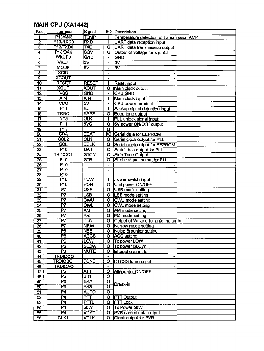
MAIN CPU ( XA1442)
1
2
3
4
5
Terminal
P13/AN3
P13/RXD0
P13/TXD0
P13/DAO
WKUPO
Siqnal I/O
TEMP I
RXD I
TXD
SQV 0
GND -
6 VREF 5V -
7
8
9
MODE
XCIN
XCOUT
XOUT
XIN
5V
XOUT 0
XIN I
TRBO BEEP
I NTS ULK
P11
SCL2 CLK
P10 DAT
TRDIOC1 STON 0
P10 STB
P10
P10
P10
P10 PSW I
P10
P7
PON 0 Unit power ON/OFF
USB 0 USB mode setting
P7 LSB
P7
P7
CWU 0 CWU mode setting
CWL 0 CWL mode setting
P7 AM o
P7 FM
P7 TUN
P6 NBS 0 Noise Brounker setting
P6
AGCS 0 AGC setting
P6 LOW 0 Tx power LOW
P6 SLOW
P6 MUTE
TRDIOCO
TONE
TRDIOAO
P5
ATT
P5 BK1 0
P5 BK2 0
P5 BK3 0
P4 AUTO 0
P4 PTT 0 PTT Output
PTTL
P4 50W 0 Tx Power 50W
VDAT
CLK1 VCLK
Description
Temperature detection of transmission AMP
UART data reception input
0
UART data transmission output
Output of voltage for squelch
GND
5V
-
5V
- -
- -
I Reset input
Main clock output
-
CPU GND
Main clock input
-
CPU power terminal
I Backup signal detection input
0
Beep tone output
I PLL unlock signal input
5V power ON/OFF output
0
Serial data for EEPROM
0
Serial clock output for PLL
0
Serial clock output for EEPROM
0
Serial data output for PLL
Side Tone Output
0
Strobe signal output for PLL
- -
-
- .
Power switch input
0 LSB mode setting
AM mode setting
0 FM mode setting
0 Output of Voltage for antenna tuner
0 Tx power SLOW
0
Microphone mute
.
0
CTCSS tone output
- -
0
Attenuator ON/OFF
Break-in
PTT Lock
0
0 EVR control data output
Clock output for EVR
0
No.
10 RESET RESET
11
12 VSS GND
13
14 VCC 5V
15 P11 BU
16
17
18 P11 5VC 0
19
20 SDA EDAT I/O
21
22 SCL ECLK
23
24
25
26
27
28
29
30
31
32
33
34
35
36
37
38 P7 NRW 0 Narrow mode setting
39
40
41
42
43
44
45 TRDIOBO
46
47
48
49
50
51
52
53 P4
54
55 P4
56
-
.
-
Page 20
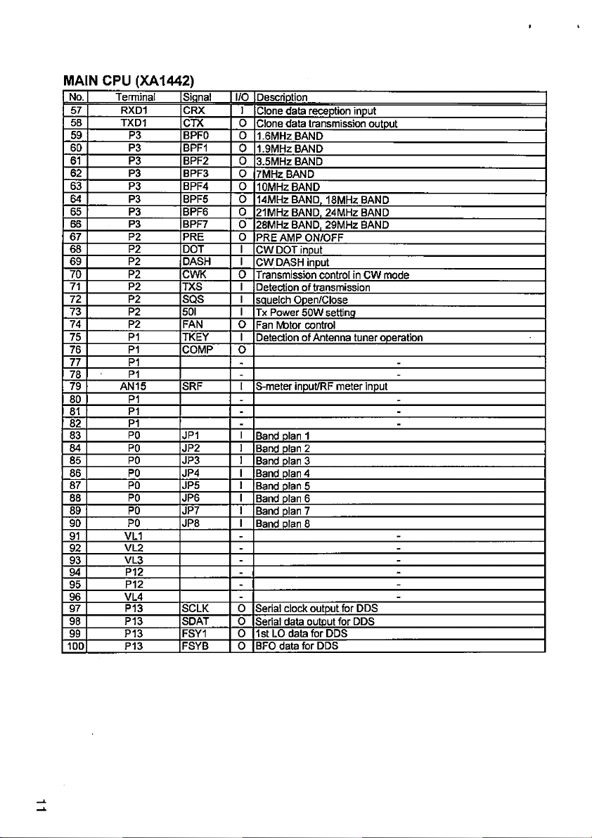
MAIN CPU ( XA1442)
No.
57
58 TXD1
59 P3
Terminal Signal I/O
RXD1 CRX I
CTX 0
BPFO 0
60 P3 BPF1
61 P3 BPF2
62 P3 BPF3
63
P3 BPF4 0
64 P3 BPF5 0
65 P3 BPF6 0
66 P3
BPF7 0
67 P2 PRE
68 P2
DOT I
69 P2 DASH I
70 P2 CWK
71 P2
TXS I
72 P2 SQS I
73 P2 50I I
74
P2
FAN 0
75 P1 TKEY I
76 P1 COMP 0
77 P1
78
P1
79 AN15 SRF I S-meter input/RF meter input
80 P1
81
P1
82 P1
83 P0 JP1
84
PO
JP2 I
85 PO JP3 ]
86 PO JP4 I
87 PO JP5 I
88 PO JP6 I
89 PO JP7 I
90 PO JP8 I
91 VL1
92 VL2
93 VL3
94 P12
95
P12
96 VL4
97 P13 SCLK 0 Serial clock output for DDS
98 P13 SDAT 0
99 P13 FSY1
100 P13 FSYB 0
Description
Clone data reception input
Clone data transmission output
1.6MHz BAND
0
1.9MHz BAND
0
3.5MHz BAND
0
7MHz BAND
10MHz BAND
14MHz BAND. 18MHz BAND
21 MHz BAND. 24MHz BAND
28MHz BAND, 29MHz BAND
0
PRE AMP ON/OFF
CWDOT inDut
CW DASH input
0
Transmission control in CW mode
Detection of transmission
squelch Open/Close
Tx Power SOW settinq
Fan IVbtor control
Detection of Antenna tuner operation
- -
- -
- -
- -
- -
I
Band plan 1
Band plan 2
Band plan 3
Band plan 4
Band plan 5
Band plan 6
Band plan 7
Band plan 8
-
- -
- -
-
-
-
Serial data output for DDS
0 1stLO data for DDS
BFO data for DDS
-
-
-
-
Page 21
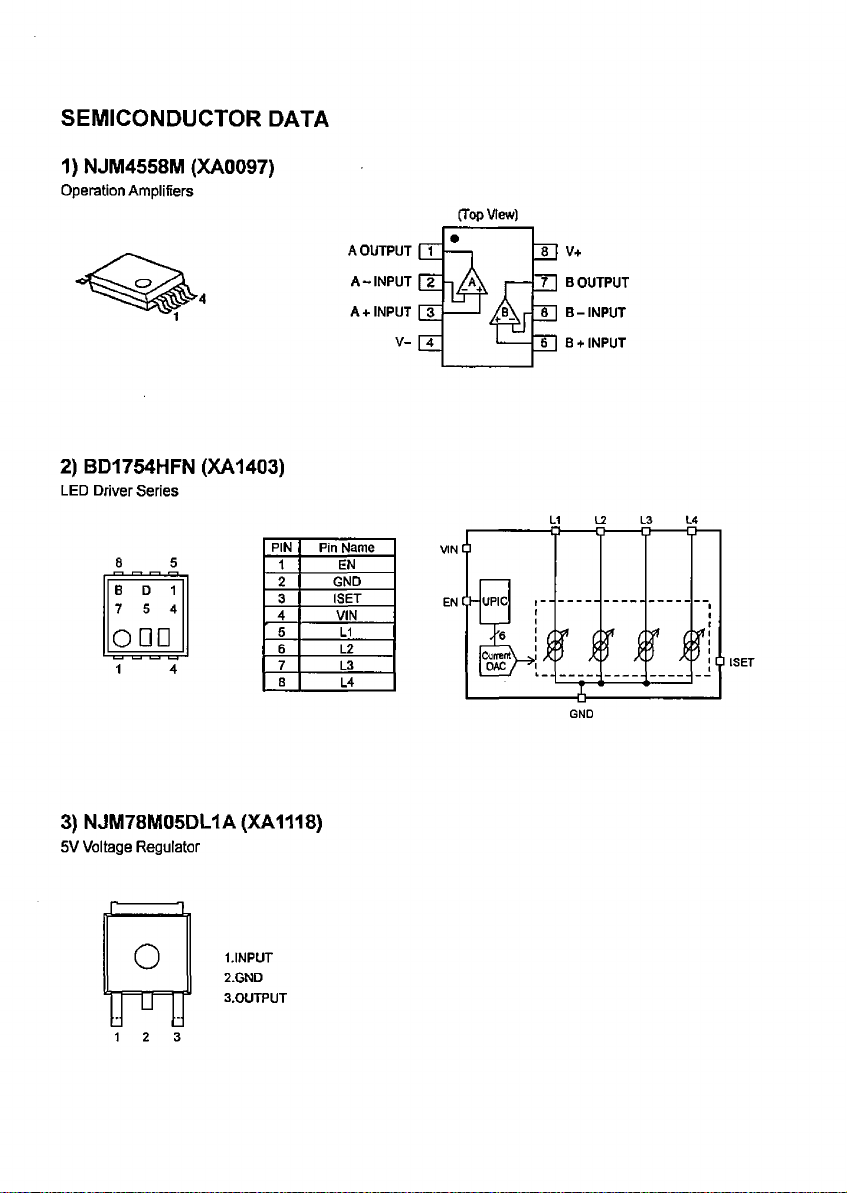
SEMICONDUCTOR DATA
1) NJM4558M (XA0097)
Operation Amplifiers
(Top View)
2) BD1754HFN (XA1403)
LED Driver Series
8 _ _ 5.
B D 1
7 5 4
o u u
l_l LJ L_1 l_J
1 4
PIN
1
2
3 ISET
4
5 L1
6 L2
7
8
3) NJM78M05DL1A (XA1118)
5V Voltage Regulator
A OUTPUT Q
A-INPUT \T_
A + INPUT [~3~
Pin Name
EN
GND
VIN
L3
L4
v - Œ
§3 v+
~7l B OUTPUT
~6~| B - INPUT
~6~| B +INPUT
1.INPUT
2.GND
3.0UTPUT
Page 22
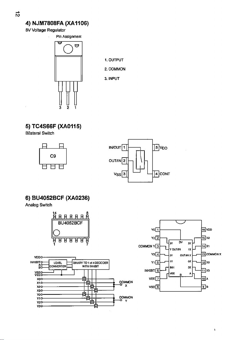
4) NJM7808FA (XA1106)
8V Voltage Regulator
Pin Assignment
3 2 1
5) TC4S66F (XA0115)
Bilateral Switch
a
____
a
C9
td td td
1. OUTPUT
2. COMMON
3. INPUT
IN/OUT
OUT/IN
Vss 3
5 Vdd
4 CONT
6) BU4052BCF (XA0236)
Analog Switch
14 8
H B R H H H B
BU4052BCF
O
1 T T H T H 1
1 7
INH1B1TC
AC
BC
CONVERTER
LEVEL
—
BINARY TO 1 ol 4 DECODER
WITH INHIBIT
—
COMMON
X
COMMON
-O y
yo|T -
Y2[T -
COMM ONY[3-
Y3[T -
Y1 |T-
iNH iBrr[6-
vh e [ 7 -
vss[?
■^37-
■ Y OUT/IN
■ INH
• VEE
16] VDD
DV
-ïs]X2
- m ] x i
- i s ] COMMON X
"iUX0
-¡ T |X 3
-w]a
Page 23
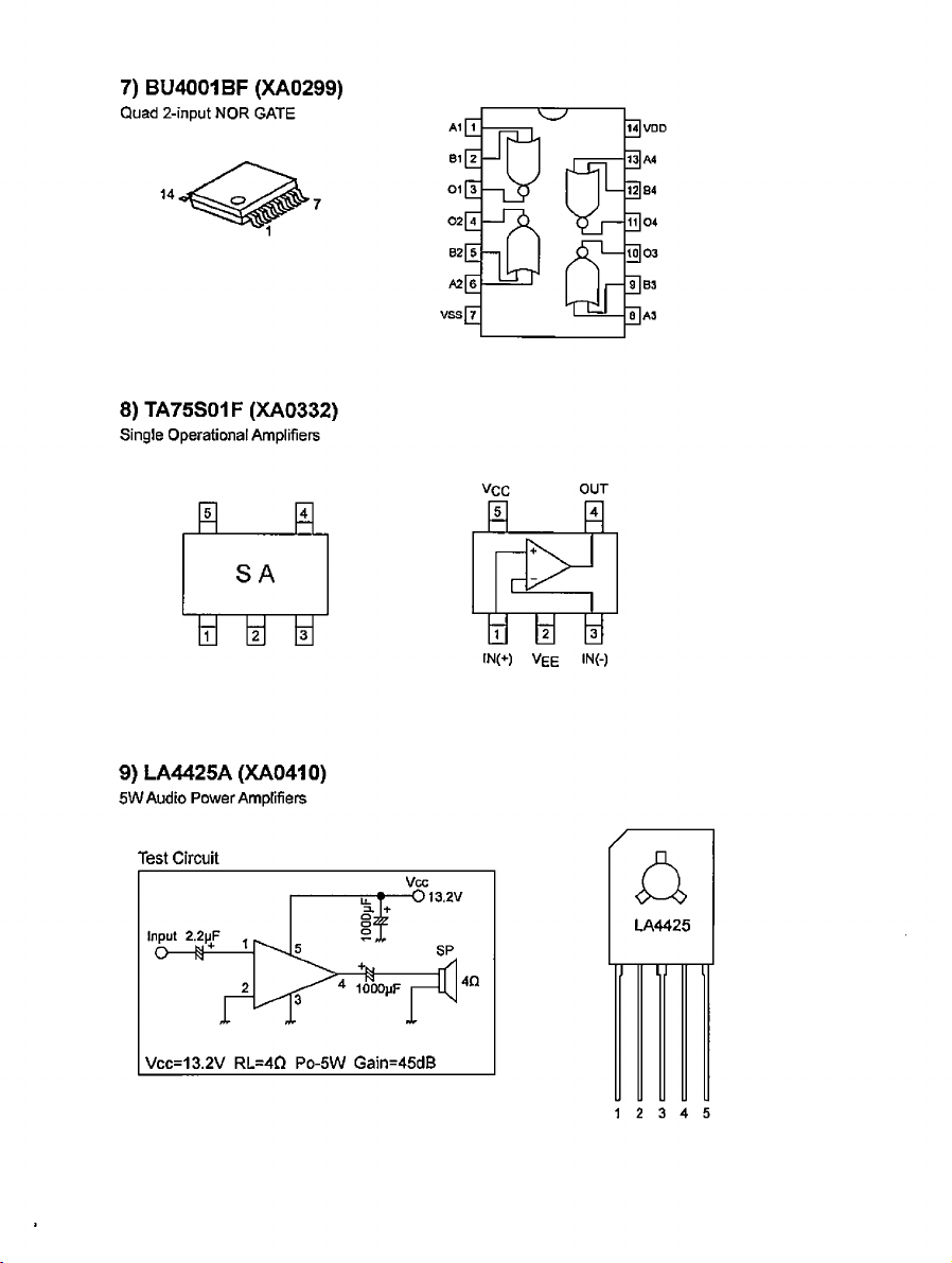
7) BU4001BF (XA0299)
Quad 2-input NOR GATE
8) TA75S01F (XA0332)
Single Operational Amplifiers
J3
_ _ _
EL
S A
p mn
14]\/0D
13] A4
12] B4
IT] 04
10] 03
T]B3
7] A3
Vcc OUT
9) LA4425A (XA0410)
5W Audio Power Amplifiers
LA4425
I
2 3 5
Page 24
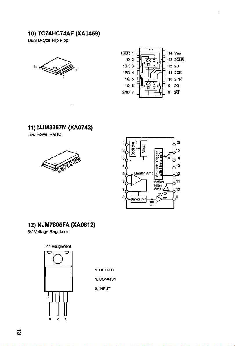
10) TC74HC74AF (XA0459)
Dual D-type Flip Flop
11) NJM3357M (XA0742)
Low Powe FM IC
1CLR 1
1D 2
1CK 3
1PR 4
1Q 5
1$ 6
GND 7
Limiter Amp
Demodulator P >
CK D
a Q
CK D
JH
a oTJ
X
¡2
T=—lr
rD
Active
Filter
Amp
|2V
] 14VCC
13 2CLR
] 12 2D
n 11 2CK
] 10 2PR
] 9 2Q
8 2G
12) NJM7805FA (XA0812)
5V Voltage Regulator
Pin Assignment
CO
1. OUTPUT
2. COMMON
3. INPUT
Page 25
13) UPC2710TB (XA0968)
Wide Band Amp
3C
2 C
1 c
□ 4
□ 5
o
□ 6
14) N JM2594V (XA0995)
Balanced Mixer
PIN
Pin Name
1
INPUT
2 GND
3 GND
4
OUTPUT
5 GND
6
Vcc
CARRIER SIGNAL
NC INPUT BYPASS INPUT
15) TC74HC390AF (XA1001)
CMOS Dual Decade Counter
1CKA 1 [
1CLR 2 [
1QA 3 [
1CKB 4 [
1QB 5 [
1QC 6 [
1QD 7 [
GND 8 [I
] 16 Vcc
3 15 2CKÄ
2 14 2CLR
] 13 2QA
] 12 2CKB
] 11 2QB
2 10 2QC
] 9 2QD
Vcc=16, GND=8
Page 26

16) MB15A01 PFV1 (XA101 0)
PLL Synthesizer
161514131211 10 9
Oscillator
[ Data I—►
1 billa teil
z _ r ~
Crystal
Control
Prescaler
64/64
128/129
1. OSC IN
2, OSC OUT
3. Vp
4. Vcc
5. Do
6. GND
7. LD
8. fin
I Programmable refere ncedlvider
I
i
Bin a ly 14-bit
referencacounter
/.v/ .m mm r /...
rTE-
/ . v t m u m m :
i 19-bilstiiftrBgister
DATA
15-bitlatcJi
19-bitshlftregister
; ::rrr rrmr rr rwr :
LE
SW
Programmabledivlder
X
Blnaly7-bit
swallo
counter
- j
Binaryl 1 -bit
programmable
counter
9. Clock
10. Data
11. LE
12. FC
13. N. C.
14. fout
15. ^ P
16. ÿ R
;
Monitor
frequency
switching
circuit
Digital lock
detector
Phase
comparator n
FC
7 p~1
T r ]
FC I
■ Í
1 7 ) L M 2 9 0 4 P W R ( X A 1 1 0 3 )
Dual Operational Amplifiers
Contra! Circuit
(Top View)
A OUTPUT IT "
A-INPUT IX
A + INPUT [jT
GND [ T
Page 27

18) LM2902PWR (XA1 106)
Quad Operational Amplifiers
1 9 ) S 8 0 8 4 5 C L N B (X A 1 1 2 0 )
C-MOS Voltage Detector
4 3
E
______B
1 2
(Top View)
Pin No.
1
2
3
4
*1. The NC pin is electrically open.
The NC pin can be connected to VDD or VSS.
Pin name
OUT Voltage detection output pin
VDD
NC*1
VSS GNO pin
Pin description
Voltage input pin
No connection
2 0 ) T C 4 S U 1 1 F ( X A 1 3 9 6 )
2 Input NAND GATE
^
______
a .
C7
ha-
5 Vqd
0OUTX
Page 28

21) TC74VHC39 3FT (XA1397)
Dual Binary Counter
1 1CK 8 2QD
2 1CLR
3 1QA 10 2QB
4 1QB
5 1QC 12 2CLR
6 1QD 13 2CK
7 GND 14 VCC
9 2QC
11 2QA
2 2 ) X C 9 5 0 4 B 0 9 2 A R ( X A 1 3 9 8 )
2ch. Step-up/Inverting DC/DC Converter
M fli E L
1pln
PIN No. Pin Name
CJ1
EXT1 External Transistor Connection 1
1
2 VDD
3
PWM1
4
5 EN1
6
PWM2
7
8 FB2
9 GND
10
Output Voltage Monitor Feedback Pin 1
FB1
EN2
Output Voltage Monitor Feedback Pin 2
EXT2
QA
FUNCTION
Supply Voltage
PWM / PFM Switching Pin 1
Enable 1
Enable 2
PWM / PFM Switching Pin 2
Ground
External Transistor Connection 2
QB
QC
QD
PWM2
Page 29

2 3 ) A D 9 8 3 3 B R M Z (X A 1 3 9 9 )
Programmable Waveform Generator
COMP [T
vdd [j[
CAP/2.5V |][
DGND [4
MCLK [F
2 4 ) R 1 E X 2 4 2 5 6 A S A S 0 A # S 0 (X A 1 4 0 1 )
256K bits CMOS Serial EEPROM
Ü VOUT
9] AQND
1] FSYNC
SCLK
D SDATA
AGND DGND VDD CAP/2.5V
SERIAL INTERFACE
AND
CONTROL LOGIC
FSYNC SCLK SDATA
■ o
R«
200(1 <
AO
A1
A2 3 6 13 SCL
GND 4 5 XI SDA
8 U VCC
1o
2
7 U
WP
Pin
Number
Remark See Dimensions for details of the package drawings.
Pin
Name
1 AO Slave address input
2 A1
3 A2 Slave address input
4
5 SDA Serial data input 1 output
6 SCL Serial dock input
7 WP
8 VCC Power supply
Slave address Input
GND Groudd
Write protection Input
Connected to Vcc: Protection valid
Connected to GND: Protection invalid
Function
Page 30

2 5 ) M 6 1 5 4 5 A F P # D F 0 R ( X A 1 4 0 2 )
Electronic Volume
V«1[T
VoutI [2
GND [3
DATA [4
2 6 ) N J M 2 0 6 8 V (X A 1 4 0 4 )
Dual Operational Amplifiers
Z 8]Vin2
7]Vout2
i
<£>
6]Vcc1
5] CLOCK
■0
CLOCK
(Top View)
A OUTPUT R ~
A-IN P U T [ T
A + INPUT I X
V- [ T
Page 31

2 7 ) T r a n s i s to r , D io d e a n d L E D o u t lin e D r a w in g s
Top View
Page 32

28) LCD Connect ion ( EL00 64)
COMMON
Page 33

Page 34

e x p l o d e d v i e w
'.LCD
to F r o n t V ie v t f
UJ0Q 72,
18
Page 35

Page 36

' ¿ S
<5 O )
é O
r f l
Page 37

b.Bottom View
AA0085 x9
UX1424.
SP0008
UE0258
DD0Q19
AD0005.
21
Page 38

c.Front View
AAQ085 x2
FG0506 x2
Page 39

PARTS LIST
TUnit
F R O r*
Ref.
Parts No.
No.
C1
C2
C3
C4
C5
C6
C7
C8
C9
C10 CU3535 ChipC
C11
C12
C13
C14
C15
C16
C17
C18
C19
C20
C21
C22
C23
C24
C25
C26
C27
C30
C31
C32
C33
C34
C35
C36
C37
C38
C39
CN1
CN2 NC
CN3
CN4
D1
D2 XD0254 Diode
D7
D8
D9 XD0230 Diode DAN202U
D10 XD0230 Diode DAN202U
D11
D12
D13
D14
D15
D16
D17
D18
D19
D20
D21 XD0402 Diode
D22
IC1
IC2
IC3
1C4 XA0947
JK1
JK2
L1
L2
LCD1
Q1
Q2
Q3
R1
R2
R3
R4
R5
R6 RK3566 ChipR 1005 1/16W220K OHMJ
CU3535
CS0424 Chip Tantalum
CU3535 ChipC
CS0424 Chip Tantalum
CU3523 Chip C
CIJ3559
CU3551
CU3559 Chip C
CU3547 Chip C
CU3547
CU3554 Chip C
CU3547 Chip C
CU3535
CLJ0118
CIJ3547
CU3523 Chip C
CU3523
CLJÛ118
OIJ3547
CU3547 Chip C
CU3547
CÜ3547
CU3547 Chip C
CU3551 Chip C
CU3547
CU3547
CU3547 Chip C
CS0470 Chip Tantalum
CS0424
CÜ3547
CU3535 ChipC
CU3535 Chip C
CU3535
CU3535
CU3535 Chip C
CU3547 Chip C
LJE0035Y
UJ0045 Connector
UE0043 Connector
XL0051
XD0254 Diode
XD0230 Diode
XD0230 Diode
XD0230
XD0230
XD0230 Diode
XDÛ230 Diode
XD0230 Diode
XD0230
XD0230 Diode
XD0230 Diode
XD0482 Diode
XD0402 Diode
XA1400 CPU
XA0097 iC
XA1403 IC
IJJ0073
UJ0072 Jack HSJ1406-01-030
QC0086
QC0086
EL0064 LCD
XIJ0236
XU0236 Transistor
XT0210 Transistor
RK3032
RK3032
RK3550
RK3522 Chip R
RK3551 Chip R
Description
ChiD C
Chip C GRM155B30J105KE18D
Chip C
ChipC
ChipC GRM36B102K50PT
Chip C
ChipC
ChipC
ChipC
Chip C
Chio C
ChipC
ChipC
ChipC GRM36B103K16PT
Chip Tantalum TMCMA1C106MTR
Chip C
ChipC
ChipC
Connector MIC FM214-8SM PYm
LED
Diode DAN202U
Diode DAN202U
Diode DAN202U
1C
Jack HSJ2630-010070
Chip Inductor
Chip Inductor
Transistor
Chip R
ChiD R
ChiD R 1005 1/16W 10K OHM J
Parts Name Version
GRM36B102K50PT
TMCMA1C106MTR
GRM36B102K50PT
TMCMA1C106MTR
GRM1552C1H101JZ01D
GRM36B223K16PT
GRM155B30J105KE18D
GRM36B103K16PT
GRM36B102K50PT
GRM36B103K16PT
GRM36B104K1 OPT
GRM36B103K16PT
GRM21BB31C475KA87L
GRM36B103K16PT
GRM1552C1H101JZ01D
GRM1552C1H101JZ01D
GRM21BB31C475KA87L
GRM36B103K16PT
GRM36B103K16PT
GRM36B1Q3K1SPT
GRM36B103K16PT
GRM36B103K16PT
GRM36B223K16PT
GRM36B103K16PT
GRM36B103K16PT
TMCMC1C107MTRF
GRM36B103K16PT
GRM36B102K50PT
GRM36B102K50PT
GRM3BB102K50PT
GRM36B102K50PT
GRM36B102K50PT
GRM36B103K16PT
HJC0282-010022
PI22A02M
VRPG3312X
1SS355
1SS355
DAN202U
DAN202U
DAN202Ü
DAN202U
DAN202U
DAN202U
DAN202U
1SS405ÎTPH3.F)
VDZT2R 5.1 B
VDZT2R 5.1 B
R5 F2L3ACAN FP#U 1
IC NJM4558M
BD1754HFN-TR
NJM7SM0SDL1A-TE1
3225 100 UH
3225 100 UH
LCD DXSR8
EMD9T2R
EMD9T2R
2SC6026MFV-GR
1608 1/1 OW 330 OHM J
1608 1/1OW 330 OHM J
1005 1/16W 47 OHM J
1005 1/16W12K OHM J
Ref.
No.
R7
R8 RK3550
R9
R10 RK3538
R11
R12 RK3543 Chip R 1005 1/16W 2.7KOHM J
R13
R14
R15 RK3538
R16 RK3550 Chip R
R17
R18 RK3550
R19 RK3538
R20 RK3550
R21
R22
R23 RK3550
R24 RK3550
R25
R26
R27
R28
R33 RK3550 ChipR 1005 1/16W10KOHM J
R34 RK3550 Chip R 1005 1/16W10KOHM J
R35 RK3550
R36 RK3550
R37 RK3550 Chip R
R38
R39 RK3550
R40 RK3570
R42 RK3550 ChipR
R43
R45 RK3550
R46
R47 RK3538 ChipR 1005 1/16W 1.0K OHMJ
R48
R49 RK3530
R50 RK3530 ChipR 1005 1/16W 220 OHMJ
R51
R52 RK3530
R53 RK3564
R54 RK3038 Chip R 1608 1/1 OW I.OKOHMJ
R55
R56 RK3550
RE1 UR0029
VR1 RV0051 Trimmer R
VR2
VR3
VR4
X1 XB0032
Parts No. Description Parts Name
RK3557 Chip R 1005 1/16W39K OHMJ
RK3538
RK3538
RK3550 Chip R 1005 1/16W 10K OHMJ
RK3550
RK3538 Chip R 1005 1/16W I.OKOHMJ
RK3550
RK3538
RK3550
RK3548
RK3538 Chip R 1005 1/16W I.OKOHMJ
RK3538
RK3550 Chip R 1005 1/16W 10KOHM J
RK3550 Chip R 1005 1/16W 10K OHM J
RK3550 ChipR
RK3538 Chip R 1005 1/16W I.OKOHMJ
RK3530 Chip R 1005 1/16W 220 OHMJ
RK3038 Chip R 1608 1/10W I.OKOHMJ
RV0051 Trimmer R
RV0053
RV0053
FM0034 MIC GND PLATE
UP0653
DG0050
FP0328 LED SPACER
FP0034 MIC SPACER DR110
FG0499 LCD RUBBER
TL0041
TL0037 DIFFUSSION SHEET
ST0103 LCD HOLDER DXSR8
Chip R
Chip R 1005 1/16W I.OKOHMJ
Chip R 1005 1/16W 1.0KOHMJ
Chip R
Chip R 1005 1/16W10K O H M J
Chip R 1005 1/16W 1.0KOHMJ
Chip R 1005 1/16W10K O HM J
Chip R 1005 1/16W I.OKOHMJ
ChiD R
ChiD R
ChiD R
Chip R 1005 1/16W 10K OH MJ
ChiD R
ChiD R
ChiD R
Chio R
Chip R 1005 1/16W10KOHM J
ChipR 1005 1/16W10KO H M J
Chip R 1005 1/16W 10KOHM J
ChipR 1005 1/16W 470K OHMJ
Chip R 1005 1/16W1 OK OHMJ
Chip R 1005 1/16W 220 OHMJ
Chip R 1005 1/16W 220 OHMJ
Chip R
Chip R 1005 1/16W 10K OHMJ
ENCODER
1005 1/16W10K OHMJ
1005 1/16W 1.0K OHMJ
1005 1/16W 10K OHMJ
1005 1/16W10KOHM J
1005 1/16W10K O H MJ
1005 1/16W I.OKOHMJ
1005 1/16W10KOHM J
1005 1/16W10KOHM J
1005 1/16W6.8K OHMJ
1005 1/16W 1.0KOHMJ
1005 1/16W10KOHM J
1005 1/16W10KOHM J
1005 1/16W10KOHM J
1005 1/16W150K OHMJ
RES16B50-201-C
RK09D1130C2PM 0KB1
RK09D1130C2PM 0KB)
Trimmer R RK09D1130C3Cf1 0KB)
Trimmer R
CERAMIC
PCB
RK09D1130C3Cf10KB)
CSTCE8M00G52-R0
DXSR8 FRONT INTEG
LCD LIGHT DXSR8
REFLET SHEET
LCD Unit
Ref.
No.
D3 XL0133
D4
D5 XL0133
D6
R29
R30
R31 RK3031
R32
Parts No. Description Parts Name
XL0133
XL0133
RK3031
RK3031
RK3031
ChiD LED
ChiD LED
ChiD LED
ChiD LED
ChiD R
ChiD R
ChÎD R
Chio R
TLWK1100CÎT11)
TLWK1100C(T11)
TLWK1100C(T11 )
TLWK1100CÎT11)
1608 1/1 OW 270 OHM J
1608 1/1 OW 270 OHM J
1608 1/1 OW 270 OHM J
1608 1/1 OW 270 OHM J
Version
Version
23
Page 40

PA Un i t
Ref.
No.
C801
C802 CU0095
C803 CU0095
C804 CU0101
C805 CU0095
C806 CU3111
C807 CÜÔ095
C808 NC
C809
C810 NIC
C811
C812 CU4017
C813 CU0095
C814 CU4051
C815 NC
C818 NC
C819
C820
C821
C822 CU0101
C823 CU0095
C824
C825 CU3111
C826 CU0101
C827
C828
C829
C830
Ó831
C832 CU3111
C833 CU0101
C834 CU3035
C835
C836 CU3111
C837 CU3047
C838
C839 CU0101
C840
C841
C842
C843 CU0101
C844 CU3047
C845
C846 CE0343
C847
C848 CU3047
C849
C850 CU3035
C851
C852
C860 ÑÓ
C861
C901
C902 CU4045
C903
Ó904 CU3027
C905 CU3047
C906 CU3047
C907 CU4051
C908
C909 CU4054
C910 CU4051
C911
C912
C913
C914 CU 3026
C915 CU3019
C916
C917 CU4022
C918 CU3111
C919
C920 CU3031 Chip C
C921
C922
C923
C924 NC
0925 NC
C926
C927 CU4027 Chip C GRM42-6X7R331K500PT
Parts No.
CUQ1Q1
CU0101
NÓ
NC
CU3011
CU3006
CU0095
CÜ3035 ChiDC
CU0095
CU3022
CU3025
CU3021
CU3035
CE0350
CU3035
CU0101
CE0353
CU3035
ÍU30 4 7
CU3047
CU3047
CU3047
CU4052
CU4051
ÑC
CU4053
CU4052
CU3029
CU3019
CU4049
CU3031
CU3047 Chip C
CU3111
NC
CU3047
Description Parts Name
Chip C
Chio C
Chip C
ChiD C
ChioC
ChiD C
ChiD C
Chio C
ChiD C
ChioC
ChiD C
ChiD C
ChiD C
ChioC
ChiD C
ChiD C
Chio C
ChiDC
ChiD C
ChiDC
Chio C
Chio C
ChiD C
ChiD C
ChiDC
Chip C
ChiDC
ChiD C
Electrolytic C
Chip C
Chio C
ChiD C
Electrolytic C
Chio C
ChiD C
ChioC
Electrolytic C
ChiDC
Chip C 1608 B 50V 0.010UF
ChioC
ChiD C
ChiD C
Chip C 1608 B 50V 0.010UF
ChiD C
ChiD C
ChiD C
ChiD C
ChioC
ChioC
ChiD C
ChiD C
ChioC
ChioC
ChiD C
ChÎD C
ChioC
ChioC
ChiDC
ChiD C
ChiDC
Chip C
ChiDC 1608 B 50V 470PFK
ChipC 1608 B25V0.1UF
Chip C
2012 B 50V 0.1 UF
2012 B 50V 0.022UF
2012 B 50V 0.022UF
2012 B 50V 0.1 UF
2012 B 50V 0.022UF
1608 B 25V 0.1 UF
2012 B 50V 0.022UF
2012 B 50V 0.1 UF
GRM42-6CH330J500fi t
2012 B 50V 0.022UF
GRM31A7U2J471JW31D
1608 CH 50V 10PFC
1608 CH 50V 5PFC
2012 B 50V 0.1 UF
2012 B 50V 0.022UF
2012 B 50V 0.022UF
1608 B 25V 0.1 UF
2012 B 50V 0.1 UF
1608 B 50V 0.001 UF
2012 B 50V 0.022UF
1608 CH 50V 82PFJ
1608 CH 50V150PF J
1608 CH 50V 68PFJ
1608 B 25V 0.1UF
2012 B 50V 0.1 UF
1608 B 50V 0.001 UF
1608 B 50V 0.001 UF
1608 B 25V 0.1 UF
1608 B 50V 0.010UF
16V100UF
2012 B 50V 0.1UF
1608 B 50V 0.001 UF
2012 B 50V 0.1UF
16V 470 UF
2012 B 50V 0.1UF
1608 B 50V 0.010UF
1608 B 50V 0.001 UF
16V1000UF
1608 B 50V 0.010UF
1608 B 50V 0.010UF
1608 B 50V 0.001 UF
1608 B 50V 0.010UF
GRM31A7U2J681JW31D
GRM31A7U2 J471JW31TT
GRM31A7U2J151JW31D
1608 CH 50V220PFJ
1608 B 50V 0.010UF
1608 B 50V 0.010UF
(5ftM31 A7U2J471JW31D
<56M31A7U2J102JW3lTr
GRM32A7U2J222JW3lfT
GRM31A7U2J471JW31D
GRM31A7U2J681JW31D
1608 B 50V 330PFK
1608 CH 50V 47PFJ
1608 CH 50V180PFJ
1608 CH 50V 47PFJ
GRM31A7U2J271 JW3fET
GRM42-6CH820J500PT
1608 B 25V 0.1 UF
1608 B 50V 470PFK
1608 B 50V 0.010UF
1608 B 50V 0.010UF
Version
Ref.
No.
C928 CU4051
C929
C930
C931 CU3111
C932 CU3111
C933
C934 CU4023
C935 CU3547
C936 CU3547
C937
C938 CU3547
C939 CU3111
C940
C941
C942 CU4052
C943 CU4051
C944
C945
C946 CU4021
C947
C948
C949 CU4045
C950 CU4027
C951
C952 CU3547
C953 CU3547
C954
C955
C956 CU3047
C957 CU304?
C958
"Ô959 CU4048
C960 CU4022
C961 CÜ3547
C962
C963 CU4015
C964
C965
£966 CU3047
C967 CU4013
C968
C969 NC
C970 CU4016
CN801
CN802
CN803 UE0041
CN901 RB0108
CN902
CN903 UE0603
CN904
D804 XD0038
D805 XD0038
D902 XD0453
D903
D904 X00430
0905 XD0430
D906 XD0430
D907 XD0391
D908
0909
0910 XD0391
D911
D912
0913
F801 EF0011
FB801
FB802 QB0070
FB803
FB804 QB0070
Parts No.
CU4050
CU4046
CU4021
CU3047
CU3047
CU4049
CU3547
CU4015
CU3047
CU3047
ÔU4023
CU4014
CU4018
CU4021
ÖU4018
CU3547
CU3047
ÜU4024
UE0041
UX1424
UÉ0603
UE0041
D801 XD0363
D802 XD0363
D803 XD0493
D806
XD0391
D901 XD0391
XDQ430
XD0391
XD0391
XD0391
XD0391
XD0391
QB0008
QB0070
FB901
QB0070
FH801
FH802
L801
L802
UH0014
UH0014
QR0024 Transformer
QR0014C
Description Parts Name
ChiD C
ChiD C
ChiD C
ChiD C
ChiD C
ChiDC
ChipC
ChiDC
ChiD C
ChiDC
ChipC
ChipC
Chip C
ChiDC
ChipC
ChiD C
ChiD C
ChipC
ChioC
ChiD C
ChiD C
ChioC
ChioC
ChiD C
ChipC
Chip C
ChiD C
ChiD C
ChipC
ChiDC
ChiD C
Chip C
ChipC
Chip C
ChipC
Chip C
ChiD C
Chip C
ChioC
ChiDC
ChiD C
ChiD C
Connector
Connector WIRE POWER
Connector
Resistor
Connector
Connector
Connector
Diode
Diode
Diode
Diode
Diode
Diode
Diode CRG01iTE85L)
Diode
Diode L709CER
Diode
Diode
Diode
Diode
Diode CRG01(+E85U
Diode CRG 0KTE85U
Diode
Diode
Diode
Diode CRG0KTE85U
FUSE
Ferrite Bead
Ferrite Bead
Ferrite Bead
Ferrite Bead
Ferrite Bead BL02RN2R1M2B
Fuse Holder
Fuse Holder
Transformer
GRM31A7U2J471JW31D
GRM31A7 U2 J391J W31D
GRM31A7U2J181JW31D
1608 B 25V 0.1 UF
1608 B 25V 0.1 UF
GRM42-6CH680J500PT
G RM42-6CH101J500PT
GRM36B103K16PT
GRM36B103K16PT
1608 B 50V 0.010UF
GRM36B103K16PT
1608 B 25V 0.1UF
1608 B 50V 0.010UF
ÖRM31A7U2J271J W31D
GRM31A7U2J681JW31D
GRM31A7U2J471JW31D
GRM36B103K16PT
GRM42-6CH220J500PT
GRM42-6CH680J500 PT
1608 B 50V 0.010UF
1608 B 50V 0.010UF
GRM31A7U2J151JW31D
GRM42-6X7R331K500PT
GRM42-6ÖH101J500PT
GRM36B103K16PT
GRM36B103K16PT
GRM42-6CH180J500PT
GfcM42-6CH390J500PT
1608 B 50V 0.010UF
1608 B 50V 0.010UF
GRM42-6CH680J500PT
G RM31A7U2J221JW31D
GRM42-6CH820J500PT
GRM36ßl03"Rl6PT
GRM42-6CH390J500PT
GRM42-6CH220J500PT
GRM36B103K16PT
1608 B 50V 0.01 OUF
1608 B 50V 0.010UF
GRM42-6CH150J500PT
3216 CH 500V120PF
GRM42-6CH270J500PT
CONNECT. TMP-J01X-V6
CONNECT. TMP-J01X-V6
1/6W TYPE 0 OHM
BIOB-PH-K-S(LFHSN)
B1GB~PH-K-S(LF){SN)
CONNECT.TMP-JOI X-V6
RLS-73f£-11
ftL0-73TE-11
FCQS30A065
1SS133
1SS133
CRG0KTE85L)
RB717F
L709CER
L709CER
L709CER
CkG 01(TE85U
CRG0KTE85U
CRG01(T£85L)
CRG01(T£85L)
FGMB125V-5A PBF
FB HF30ACB201209
BL02RN2R1M2B
BL02RN2R1M2B
BL02RN2R1M2B
PFC5000-0301
PFC5000-0301
RF TRANS QR0024
RF TRANSF.QR0014C
Version
24
Page 41

PA Un it
Ref.
No.
L803
L804
L805
L806
L807
L808 QR0012
L809
L901 QR0013A
L902
L903
L904 QC0126
L90á
L90S
L907
L908 QR0007
L909
L910
L911
L912 QC0087
L914 QR0011
L915 QR0010
L916 QC0048
L917 QKA75H
L918
L919 QC0048
L920
L921
L922
L923 RD1013
Q801 XE0056
Q802 XE0055 FET
Q803
Q804 XE0055
Q805
Q806 XU0210
Q901 XU0210
Q902 XU0210
Q903
Q904 XU0236
Q905
Q906
Q907
Q908
R801
R802 RK3038
R803 RK4028
R804 RE0046
R805
R806 RK0001
R807 &K3044
R808 RK0052
R809
R810 RK3015
R811
R812 NC
R813 NC
R814 RK0052
R815 RK0056
R816 RK0001
R817 RK3033
R818 RK3033
R819 RK3023
R820
R821 RK4095
R822 RE0046
R823 RK4028
R824 RK0018
R825 RK0035
R826 RK0039
R827
R828
R829 RK3038
R830
R831
R832
R833
R834 RK0039
R835
R836
Parts No.
QR0025
QC0043
QC0129
QC0129
QR0012
QRQQ12
QR0021
QR0004 •
QC0126
QC0087
QR0006
ÜÜ0087
QR0009A Troidal Coil
QR0008
QKA65H
QKA45H
ÛKA55H
QC0048
XE0054
XE0056 FET
XU0236
XU0236
XU0236
XU0236
XU0236
&K3038
RK4095
S~K0056
RK4095
RK4085
RK4051
RK4051
RE0045
RK1025
RK0031
RK3038
RK0005
RK3062
Description
Transformer
ChiD Inductor
Chip Inductor
ChiD Inductor
Troidal Coil
Troidal Coil TROIDAL COIL QR0012
Troidal Coil TROIDAL COIL QR0012
Troidal Coil
Troidal Coil
Troidal Coil TROIDAL COILQR4
ChiD Inductor
ChiD Inductor
Chip Inductor
Troidal Coil TROIDAL COIL QR0006
Troidal Coil
ChiD Inductor
Troidal Coil TROIDAL COIL QR0008
ChiD Inductor
Troidal Coil TROIDAL COIL QR0011
Troidal Coil
Chio Inductor
Air Core Coil
Air Core Coil
Air Core Coil
Air Core Coil MR10.0 4.5T1.0
Air Core Coil
ChiD Inductor
Resistor 1/4W TYPE 0 OHM
FET
FET RD06HHF1-01
FET RD100HHF1 -01
Transistor RN1107FV
Transistor RN1107FV
Transistor
Transistor EMD9T2R
Transistor EMD9T2R
Transistor
Transistor EMD9T2R
Transistor EMD9T2R
Transistor EMD9T2R
ChiD R
Chip R
ChiD R
Resistor MOS3CT521A180 J
ChiD R RK73 B2ETTD102 J
iChipR
ChiD R
ChiD R
ChiD R
ChipR
ChiD R
Chip R 2125 1/8W10K OHM J
ChiD R
ChiD R
ChiD R
ChiD R
Chip R
ChiD R
ChiD R
Resistor MOS3CT521A180J
ChiD R
ChiD R
ChiD R
ChiD R
ChiD R
ChiD R
Chip R
Resistor MOSX3CT521A4R7J
ChiD R
ChiD R
ChiD R
ChiD R
ChiD R
Chio R
Parts Name
RF TRANS QR0025
3225 2.2 UH
3225 .39 UH
3225 .39 UH
TROIDAL COIL QR0012
TROIDAL COIL QR0013A
TROIDAL COIL QR0021
3225 .22 UH
3225 .22 UH
3225 120 UH
TROIDAL COIL QR0007
3225 120 UH
TROIDAL C01LQRQQ09A
3225 120 UH
TROIDAL COIL QR0010
3225 10 UH
MR1O.0 7 .5 fl.0
MR10.0 6.5T 1.0
3225 10 UH
MR10.0 5.5T 1.0
3225 10 UH
RD16HHF1-01
RD100HHF1-01
RD16HHF1-01
RN1107FV
EMD9T2R
1608 1/10W1.0KOHM J
1608 1/10W1.0KOHM J
4532 1/2W 150 OHMJ
2125 1/8W10 O HMJ
1608 1/10W3.3KOHM J
2125 1/8W10K OHMJ
2125 1/8W22K OHMJ
1608 1/10 W 12 OHMJ
RK73B2ETTD102J
2125 1/8W 22K OHM J
2125 1 /8 W 10 OHMJ
1608 1/10W 390 OHMJ
1608 1/10W 390 OHMJ
1608 1/10W56 OHM J
3225 1/4W 8.2 OHMJ
RK73B2ETTD102J
4532 1/2W150 OHMJ
2125 1 /8W 100 OHM J
21251/8W1 KOHM J
2125 1/8W 2.2KOHM J
3225 1 /4W 100 OHM J
3225 1/4W 100 OHM J
1608 1/10W1-OKOHM J
3216 1/8 W 330 O H MJ
2125 1/8W 680 O HM J
1608 1/1ÛW 1-OKOHM J
2125 1/8W2.2KOHM J
2125 1/8W22 O HM J
1608 1/10WIOOKOHM J
Version
Réf.
No.
R837 RK0107
R901
&902 RK4029
R903 RK0065
R904
R905 RK0107
R906 RK3001
R907
R908 RK3050
R909 RK3050
R910
R911
R912 RK3052
R913 RK3062
R914 RK3062
R915
R916
R917 RK3023
R918
R919 RK3538
R920
R921 RK3538
R922
fî923 RK3538
RL801
RL901
RL902
RL903
RL904
RL905 UL0006
RL906
RL907 UL0006
RL908
RL909 UL0006 Relay
RL910
RL911
RL912
RL913
RL914
SA901
TC901
TH801
TP801 NC
TP802 UE0047
TP803 UE0047
TP804 ÜE0047
TP806 UE0047
TP808 UE0047
TP809
ÎP 8 10 UE0047
TP811
TP901 NC
VR801 RH0276
VR802
VR803 RH0276
VR804 RH0206
W801 RD0108
Ref.
No.
C101
C102 CU3547
C103 CU3111
C104 CU3111
C105
C106 CU3554
C107
CÏ08 CU3523
C109 CU3559
Parts No. Description
RK3001
RK4024
NC
RK3034
RK3052
RK3538
RK3538 Chip R
RK0008
RK3538
SK3538
UL0029
UL0006
UL0006
UL0006
UL0006
UL0006
UL0006
UL0006
UL0006
UL0006
UL0006
UL0006
EU0002 Surqe
CT0059 Trimmer
XS0063
I H805
NC
IHÖU/ NO
UE0047
NC
RH0206 Trimmer R
QB0069
TZ0066
UP0655 PCB
UP0318
TT1001 0.7X1 MM
FM0220 GROUND PLATE DR620
YZ0042 CEMENT G 17 /1G
Parts No.
CU3547
CU3547
CÜ3523
Chip R
Chip R
Chip R
Chip R
Chip R
Chip R
ChiD R
ChiD R
ChiD R
ChiD R
ChiD R
Chip R
ChiD R
ChiD R
Chio R
Chip R
ChiD R
ChiD R
ChiD R
ChiD R
Chio R
ChiD R
Relav
Relay
Relav
Relav
Relav
Relav
Relav
Relav
Relav
Relav
Relav
Relav
Relay
Relav
Thermistor
Connector
Connector
Connector
Connector
Connector
Connector
Connector
Trimmer R
Trimmer R
Trimmer R
Resistor
Description
Chip C
ChiD C
ChiD C
ChiD C
ChiD C
ChiD C
ChiD C
ChiD C
ChiD C
Parts Name
2125 1/8W0OHM
1608 0 OHM
4532 1/2 W180 OHM J
2125iy8 W 68K OHMJ
4532 1/2W 68 OHM J
2125 1/8WOOHM
1608 0 OHM
1608 1/10W 10K OHMJ
1608 1/10W10K OHM J
1608 1/10W 470 OH MJ
1608 1?10W15K OHM J
1608 l7lOW 15K O HM J
1608 1/10W100KOHM J
1608 1/1OWIOOKOHMJ
1005 1/16 W 1.OK OHMJ
1005 1/16W1.0KOHMJ
1608 1/10W 56 O HM J
2125 1/8W33 OHM J
1005 1/16 W 1.OK OHMJ
1005 1/16 W 1.OK OHMJ
1005 1/1 6W 1.OK OHMJ
1005 1/1 6W 1.OK OHMJ
1005 1/16W 1.oRTt)HMJ
G5NB-1A DC 12V
AG201344
AG201344
AG201344
AG201344
AG201344
AG201344
AG201344
AG201344
AG201344
AG201344
AG201344
AG201344
AG201344
AG201344
SA05CT52A301N
CV05D2001C
GA13-3H103JB
ROUND PIN R9X10
ROUND PIN R9X10
ROUND PIN R9X10
ROUND PIN R9X10
ROUND PIN R9X10
ROUND PIN R9X10
ROUND PIN R9X10
VZ067TL1B222
PVA2A102A01ROO
VZ067TL1B222
PVA2A102A01ROO
1/6 W Y Y P^0 0HM
HF70RH10X20X5
ACC, FOR 2SC1971/01
DXSR8 PA INTEGRATED
DXSR8 QR0024F TRANS
Version
Parts Name Version
GRH/Í36B103K16PT
GRM36B103K16PT
1Ö08 BÜSV 0.1 Uh
1608 B 25V 0.1 UF
GRIÜ36B103K16PT
ÔRM366104K10PT
GRM1552C1H101JZ01D
GRM1552C1H101JZ01D
GRM155B30J105KE18D
25
Page 42

MAIN U nit
Ref.
Parts No.
No.
C110 CU3517
c m
C112 CU3547
C113
C114 CU3543
C115 CU3543
C116 CU3565
C117
C118 CU3553
C119
C120 CU3547
C121 CU3511
C122 CU3547
C123
C124 CU3535
C125 CU3518
0126 CU3513
C127
0128 CU3531
C129 CU3525
C130 CU3553
C131 CU3512
C132 CU3512
C133 GU3508
C134
C135 CU3527
C136 CU3547
C137
C138
C139 CU3554
C140 CU3585
C141 CU3553
C142 CU3553
C143 CU3547
C144 CU3547
C145 CU3547
C146 CU3553
C147
C148 CU3547
C149
C150
C151 CU3551
C152 CU3111
C153 CU3547
C154 CU3041
C155 CU3023
C156 CU3038
C157 CU3528
C158
C159 CU3553
C160 CU3037
C161 CU3111
C162 CU3035
C163
C164
C165 CU3553
C166 CU3553
C167
C168
C169 CU3547
C170 CU3554
C171
C172
C173 CU3547
C174
C175 CU3531
C176 CU3531
C177 CU3531
C178 CU3101
C179
C180 CU3037
C181 CU3547
C182 CU3547
C183 CU3547
C184 CU3547
C185 CU3547
C186 CU3547
C187 CU3547
C188 CU3547
CU3517
CU3504
CU3553
CU3545
CU3554
CU3509
CU3524
CU3512
CU3553
CU3553
CU3553
CU3535
CU3111
CU3035
CU3531
CU3038
CU3051
CU3553
CU3515
CU3027
CU3038
Description Parts Name Version
ChiD C
ChipC
ChiDC
ChiD C
ChipC
ChipC
ChiDC
ChiD C
Chip C
ChiD C
ChiD C
ChiD C
ChipC
ChiD C
ChiD C
ChiDC
ChioC
ChiD C
ChiD C
ChioC
ChiD C
ChiD C
Chip C GRM36CH120J50PT
ChipC
ChiD C
Chip C
ChipC
ChipC
ChiD C
ChipC
ChiDC
ChiDC
ChiD C
ChioC
ChiDC
ChiD C
ChiDC
ChiDC
ChiD C
ChiDC
ChiDC
ChiD C
ChipC
ChipC
ChiDC
ChiD C
ChiD C
Chip C
ChiD C
ChipC
ChiD C
ChiD C
ChiD C
ChipC
ChiDC
ChiDC
ChiD C
ChipC
ChiDC
ChiD C
ChiD C
ChipC
ChiDC
ChiD C
ChiD C
ChipC
ChioC
ChiD C
ChiD C
ChipC
ChioC
ChiD C
ChÎD C
ChioC
ChiDC
ChiD C
ChioC
ChiDC
ChÎD C
GRM36CH330J50PT
GRM36CH330J50PT
GRM36B103K16PT
üttM36ÔJ030CèOPT
Í3RM36B472K25PT
GRM36B472K25PT
GJM1552C1H5R0FB01D
GRM36B473K10PT
GRM36B473K10PT
1005 B 25V 0.0068UFK
GRM36B103K16PT
GRM36CH100D50PT
GRM36B103K16PT
GRM36B104K10PT
GRM36B102K50PT
GRM36CH390J50PT
GRM36CH150J50PT
GRM36CH080 D50PT
GRM36B471K50PT
GRM1552C1H151JD01D
GRM36B473K1 OPT
GRM36CH120J50PT
1005 CH 50V7 P FD
GRM1552C1H121JA01D
GRM1552C1E221JD01D
GRM36B103K16PT
GRM36CH120J50PT
GRM36B473K10PT
GRM36B104K10PT
GRM155B31A474KE14D
G RM 36 B473K1 OPT
GRM36 B473K1 OPT
GRM36B103K16PT
GRM36B103K16PT
GRM36B103K16PT
GRM36 B473K1 OPT
GRM36 B473K1 OPT
GRM36B103K16PT
GRM36 B473K1 OPT
GRM36B102K50PT
G RM 36 B223K16PT
1608 B 25V 0.1 ÙF
GRM36 B103K16 PT
1608 B 50V 0.0033UF
1608 CH 50V100PFJ
1608 B 50V 0.0018UF
GRM1552C1E271JD01D
1608 B 25V 0.1 UF
GRM36B473K10PT
1608 B 50V 0.0015UF
1608 B 25V 0.1 UF
1608 B 50V 0.001 UF
1608 B 50V 0.001UF
GRM36B471K50PT
GRM36B473K10PT
GRM36B473K10PÍ
1608 B 50V 0.0018UF
1608 B 50V 0.022UF
GRM36B103K16PT
GRM36B104K1 OPT
GRM36B473K1 OPT
GRM36CH220J50PT
GRM36B103K16PT
1608 CH 50V220PFJ
GRM36B471K50PT
GRM36B471K50PT
GRM36B471K50PT
1608 B 50V 0.047UF K
1608 B 50 V 0.0018UF
1608B5 0 V 0.0015UF
GRM36B103K16PT
GRM36B103K16PT
GRM36B103K16PT
GRM36B103K16PT
GRM36B103K16PT
GRM36B103K16PT
GRM36B103K16PT
GRM36B103K16PT
Réf.
Parts No. Description
No.
C189 CU3037
C190 CU3035
C191 CS0436
C192 CU3553
C193 CU3553
C194 CU3535
C195 CU3553
C196 CU3553
C197 CU3547
C198
CU3553
C199 CU3553
C200
CU3024
C201 CU3582
C202
£U3553
C203 CU3553
C204
CU3101
C205
CU3110
C206
CU3035
C207 CU3047
C208 CU3101
C209
C210
C211
C212
£213 CU3033
C214 CU3032
C215
C216 CU3513
C217 CU3022
C218
C219 CU3535
C220
C221
C222 CU3101
C223
C224 CU3031
C225 CU3044
C226 CU3101
C227 CU3554
C228
C229
C230
C231 CU3510
C232 CU3535
C233
C234 CU3522
C235 CU3513
C236
£237 CU3512
C238
C239
C240
C241 CU3547
C242 CU3554
C243 CU3547
C244 £Ü3547
C245 CU3101
C246 CU3031
C247 CU3029
C248 CU3040
C249 CU3101
C250 CU3554
C251 CU3554
C252 CU3523
C253 CU3522
£261 CU3547
£267
CE0364
CU3553
CU3047
CU3547
CU3535
CU3547
CU3518
CU3518
CU3032
CU3031
CU3030
CU3554
CU3019
CU3519
CU3505
CU3510
CU3512
C254 CU3554
C255 CU3554
CU3029
C256
CU3028
C257
C258 CU3553
C259 CU3554
C260 CU3535
C262 CU3017
C263 CU3554
C264 £U3554
C265 CU3101
C266
CU3029
CU3027
Parts Name Version
ChiDC
ChiDC
ChiD Tantalum
ChiD C
ChiDC
ChioC
ChiDC
ChiD C
ChioC
ChiD C
ChiD C
ChiDC
ChioC
ChiDC
ChiD C
ChiDC
Chio C
Chio C
Chio C
ChioC
Electrolytic C 16V47UF
ChiD C
Chio C
ChioC
ChiD C
Chio C
ChioC
ChioC
ChioC
ChiD C
ChioC
ChiDC
ChiD C
ChioC
ChiD C
ChiD C
ChiDC
ChiDC
ChiD C
Chio C
ChioC
ChiD C
Chip C
ChipC
ChioC
ChiD C
ChipC
ChioC
ChiD C
Chip C
ChipC
Chip C
ChiD C
Chip C
ChipC
ChipC
ChiD C
ChipC 1608 B 50V 470PFK
ChioC
ChiD C
ChiD C
Chip C GRM36B104K10PT
ChioC
ChiDC
ChiD C
ChiD C
Chip C GRM36B104K10PT
Chip C
Chip C
Chip C GRM36B473K1 OPT
Chip C
ChiDC
ChiDC
Chip C
ChioC
ChiD C
ChiDC
ChioC
ChiD C
1608 B 50V 0.0015UF
1608 B 50V 0.001 Uf^
TMCMB1C336M
GRM36B473kl0PT
GRM36B473K10PT
GRM36B102K50PT
GRM36B473K10PT
GRM36B473K10PT
GRM36B103K16PT
GRM36B473K10PT
GRM36B473K10PT
1608 CH 50V120PFJ
GRM155B31A154KE18D
GRM36B473K10PT
GRM36B473K10PT
1608 B 50V 0.047UFK
16Q8“b50V0.0012UF
1608 B 50V 0.001 UF
1608 B 50V 0.010UF
1608 B 50V 0.047UF K
GRM36B473K1 OPT
1608 B50V0.010UF
GRM36B103K16PT
1608 B 50V 680PFK
1608 B 50V 560PF K
GRM36B102K50PT
GRM36CH150J50PT
1608 CH 50V 82PFJ
GRM36B103K16PT
GRM36B102K50PT
GRM36CH390J50PT
GRM36CH390J50PT
1608 B 50V 0.047UF K
1608 B 50V 560PF K
1608 B 50V 470PFK
1608 B 50V 0.0056UF
1608 B 50V 0.047UFK
GRM36B104K10PT
1608 B 50V 470PF K
1608 B 50V 390PFK
GRM36B104K10PT
1005 CH 50V 9 PF D
GRM36B102K50PT
1608 CH 50V 47 PF J
GRM1552C1H820JD01D
GRM36CH150J50PT
GRM36CH470J50PT
GRM36CH120J50PT
GRM36CH040C50PT
1005 CH 50V 9 PFD
GRM36CH120 J50 PT
GRM36B103K16PT
GRM36B104K10PT
GRM36B103K16PT
GRM36B103K16PT
1608 B 50V 0.047UFK
1608 B 50V 330PFK
1608 B 50V 0.0027UF
1608 B 50V 0.047UFK
GRM36B104K10PT
GRM1552C1H101JZ01D
GRM1552C1H820J D01D
GRM36B104K10PT
1608 B 50V 330P FK
1608 CH 50V270PFJ
GRM36B104K1 OPT
GRM36B102K50PT
GRM36B103K16PT
1608 CH 50V 33PFJ
GRM36B104K10PT
GRM36B104K10PT
1608 B 50V 0.047UF K
1608 B 50V 330PF K
1608 CH 50V220PF J
26
Page 43

MAIN Unit
Ref.
No.
C268
C269 CU3101
C270
C271
C272
C273 CU3016
CZ74
C275
C276
C277 CU3025
C278
C279
C280
C281 CU3023
C282
C283
C284
C285
C286
C287
C288
C289
C290
C291 CS0424
C292
C2Ü3
C294
C295 CU3553
C296
C297
C298 CU3137
C299
C300
C301
C302
C303
C304
C305 £U3547
C306
C3D7
C308
C309
C310
C311 CU3553
C312
C313
C314 CU3547
C315
C316
C317
C318
C319
C320
C321
C322
C323
C324
C325
C326
C327
C328
C329
C330
C331
C332
C333
C334
C335
C336
C337 CU3553
C338
C339 CU3553
C340
C341 CU3523
C342
C343
C344 CU3553
C345
C346
Parts No.
CU3038
CU3547
CU3027
CU3025
CU3521
£U3101
ÏÏU 3027
CU311Q
CU3101
CU3025
CU3014
CU3101
CU3025
CU3024
CU3034
tU 31 01
£U3101
CU3547 ChipC
CU3547
£U3554
ÔSU424
CU3552
£U3547
CS0424
CU3554
£U3547
CU3547
CU3553
CU3553
¿U3547
ÔU3545
CU3529
CU3584 ChiDC GRM155B31A334KE14D
£U3553
CU3553
CU3553
£U3551
Ci>0424
CU3547
CU3553
£U3554
ÓU3554 ChioC GRM36B104K10PT
CU3553
CU3553
CU3539
£U 3527
CU3539
CU3137
CU3553
CU3531
CU3553
CU3553
CU3553
CU3531
CU3553
CU3553
CU3547 ChiD C GRM36B103K16PT
CU3553
CU3583
CU3551
CU3553
£U 3554 ChiDC GRM36B104K10PT
CU3553
CU3554
CU3554
Description
ChiD C
ChiD C
ChiD C
ChiD C
ChiD C
ChiD C
Cfiio C
ChiD C
ChiD C
ChiD C
ChiD C
ChiD C
ChiD C
ChiD C
Chip C
ChiD C 1608 B 50V 0.047UFK
ChiD C
Chip C 1608 CH 50V120PFJ
ChiD C 1608 B 50V 820P FK
ChiD C
ChiD C 1608 B 50V 0.047UFK
ChiD C
ChiD Tantalum
ChipC
ChiD Tantalum
ChiDC GRM36B333K10PT
ChiD C
ChioC
ChiD Tantalum
ChiD C
ChiDC GRM36B104K10PT
ChiDC GRM36B103K16PT
ChiD C
ChipC
ChiD C
ChiD C
ChipC
ChipC
ChiDC
ChioC
ChiD C
ChiD C
ChipC
ChiD C
ChiD C
Chip Tantalum
ChioC GRM36B 1 0 3 ^ 6 ^
ChiD C
ChiD C
ChioC
ChiD C
ChiDC GRM36B222K50PT
ChipC
ChiD C GRM36B222K50PT
ChiD C GRM188B31C105KA92D
ChipC GRM36B473K10PT
ChipC
ChipC
ChiD C
ChiD C
ChioC
Chic C
ChiD C
ChioC
ChioC
ChiD C
ChiD C
ChioC
Chip C
ChiD C
ChiD C
ChiDC GRM36B473K10PT
ChiD C
ChiD C
Parts Name Version
1608 B 50V 0.0018UF
1608 B 50V 0.047UFK
GRM36B103K16PT
1608 CH 50V220PPJ
1608 CH 50V150PFJ
1608 CH 50V 27PFJ
GRM1552C1H680JZ01D
1608 B 50V 0.04 7bPk
1608 CH 50V220PFJ
1608 CH 50V150PFJ
1608 B 50V0.0012UF
1608 B 50V 0.047UFK
1608 CH 50V150P FJ
1608 CH 50V100P FJ
1608 CH 50V 18PFJ
1608 CH 50V150P F J
1608 B 50V 0.047UFK
GRM36B103K16PT
GRM36B103K16PT
TMCMA1C106MTR
GRM36B104K10PT
IMCMA1C1 OdM IK
GRM36B473K10PT
GRM36B103K16PT
TMCMA1C106MTR
GRM188B31C105KA92D
GRM36B103K16PT
GRM36B473K1 OPT
GRM36B473K10Pt
GRM36B103K16PT
GRM36B103K16PT
1005 B 25V 0.0068UFK
GRM36B331K50PT
GRM36B473K10PT
GRM36B473K1 OPT
GRM36B473K10PT
GRM36B473K10PT
G RM36B223K16PT
GRM36B103K16PT
I MUMA1C106M I K
GRM36B473K10PT
GRM36B104K1 OPT
GRM36B473K10Pt
GRM36B473K10P?
GRM1552C1E221JD01D
GRM36B471K50PT
GRM36B473K1 OPT
G RM36 B473K1 OPT
GRM36 B473K1 OPT
GRM36B471K50PT
GRM36B473K10PT
GRM36B473K10PT
GRM36B473K1 OPT
GRM155B31A224KE18D
GRM36B473K10PT
G RM36 B223K16PT
GRM36B473K10 PT
GRM36B473K10PT
GRM1552C1H101JZ01D
GRM36B473K1 OPT
GRM36B104K10PT
GRM36B104i<10f!>T
Ref.
No.
£347
C348
£349
C350 CU3525
C351
C352 NC
C353 CU3517
C354
£355
C356 CU3553
C357
£358 CU3554
£359 CS0424
£360 CU3554
£361
C362
C363
C364 CU3554
C365
£366
£367 CU3521
C368 CU3559
C369
£370 CU0118
C371
C372
C373
£374 CU3553
£375 CU3535
£376
C377 CU3137
C378 CU3541
£379
C380
£381 CS0424
C382
£383
C384
£385 CU3553
C386
£387
C388
C389
C390 CU3554
£391 CU3526
£392 CU3538
C393
G394
C395 CS0367
£396 CU3554
C397
C398 CU3027
C399
£400 CU3047
C401
£402 CU3047
C403 CU3047
C404
£405
£406 CS0424
£407
C408
£409
C410 CU3547
C411 CU3547
C412
C413 CU3047 ChiD C
£414 CU3554
C415 CU3047
C416
£417
£418 CU3547
C419 CS0424
C420 CU3137
£421
¿422 CU3547
C423
C424 CU3547
C425 CU3138
Parts No. Description Parts Name Version
CU3553
CU3553
CU3547
CS0424
CU3529
CU3553
CU3554
CU3554
CU3554
CU3137
CU3551
CU3547
CU3535
CS0424
CU3553
CU3553
CU3535
CU3541
CU3535
CU3547
CU3543
CU3553
CU3554
CE0353
CE0352
CU3585
CE0351
CU3554
CU3559
CE0339
CE0364
CEO339
CU3047
CU3547
CU3547
CU3137
CU3547
CU3047
CU3137
CU0123
CU3547
ChiD C
ChiD C
ChiDC
ChiD C
ChiD Tantalum
Chic C
ChiD C
Chip C
ChiD C
ChiDC
ChiD C
Chip Tantalum
ChipC
ChiD C
ChiD C GRM36B104K10PT
ChiD C
ChiD C
ChiD C
ChiD C
ChipC
ChipC
ChiD C
ChiD C
ChiD Tantalum
ChiD C
ChiD C
ChiDC
ChipC
ChiD C
Chip C
ChiD C
ChiD C
ChiDC
Chic Tantalum
ChipC
ChiD C
ChiD C
ChiD C
ChiDC
Electrolytic C
Electrolytic C
Chio C
ChiD C
ChiD C
ChiDC
Electrolytic C
ChipC
Chip Tantalum
ChiD C
ChiD C
ChiDC
Electrolytic C
Chio C
Electrolytic C
ChiD C
Chio C
Electrolytic C
ChiDC
Chip Tantalum
ChiDC
ChiD C
ChiDC
ChiD C
ChiDC
Chio C
ChiDC
ChioC
ChiDC
ChiD C
Chip C
Chip Tantalum
ChiDC
ChiD C
ChiDC
ChiDC
Chip C
Chip C
GRM36B473K1 OPT
GRM36B473K10PT
GRM36B1Q3K16PT
GRM1552C1H151JD01D
TMCMA1C106MTR
GRM36CH330J50PT
GRM36B331K50PT
GRM36B473 K1 OPT
GRM36È473K10PT
GRM36B104K1 OPT
GRM36B104K1 OPT
TMCMA1C106MTR
GRM36él 04K1 OPT
GRM36B104K1 OPT
GRM188B31C105KA92D
GRM36B1Q4K10PT
0RM36B223K16f>t
GRM36B103K16PT
GRM1552C1H680JZ01D
GRM155B30J105KE18D
GRM36B102K50PT
GRM21BB31C475KA87L
TMCMA1C106MTR
GRM3SB473KÍ0PT
GRM36B473K1 OPT
GRM36Ë473K10PT
GRM36B102K50PT
GRM36B102K50PT
GRM188B31C105KA92D
GRM36B332K50PT
ÔRM36B332K50PT
GRM36B102K50PT
TMC M Al£l06MTR
GRM36B103K16PT
GRM36B472K25PT
GRM36B473K1 OPT
GRM36B473K1 OPT
GRM36B104K10PT
16V470UF
16V 330ÜF
GRM155B31A474KE14D
GRM36B104K1 OPT
GRM1552C1E181JD01D
ÔRM36Ô182K50PlTJ
16V 220UF
UKM36b104K10P I
6.3V 10UF
6^M 36B104K10PT
GRM155B30J105KE18 D
1608 CH 50V220PFJ
16V 10UF
1603 B 50V 0.010UF
16V 47UF
1608 B 50V 0.010UF
1608 B 50V 0.010UF
16V 10UF
1608 B 50V 0.010UF
TMCMA1C106MTR
GRM36B103K16PT
GRM36B103K16PT
GRM188B31C105KA92D
GRM36B103K16PT
GRM36B103K16PT
GRM36B103K16PT
1608 B 50V 0.010UF
GRM36B104K10PT
1608 B 50V 0.010UF
1608 B 50V 0.010UF
GRM188B31C105KA92D
GRM36B103K16PT
TMCMA1C106MTR
GRM188B31C105KA92D
GRM21BB31E155KA87L
GRM 36IÏ03K16PT
GRM36B103K16PT
GRM36B103K16PT
GRM188B31C225KE14D
27
Page 44

MAIN U nit
Ref.
Parts No.
No.
C426 CU3547
C427 CU3137
C428
C429 CU3535
C430 CU3138
C431
Ó432
C433
C434 CU3137
C435 CU3S54
C436
C437 CU3547
C438 CU3547
C439 CU3547
C440 CU3553
C441
C442
C443 CU3547
C444 CU3547
C445 CU3547
C446 CU3547
C447 CU3137
C448 CU3047
C449 ÓÜ3047
C450 CU3047
C451
C452 CU3547
C453
C454 CU3554
C455 CU3559
C456 CU3543
C457 CÍU3547
C458 CU3547
C459 CS0424
C460 CU3544
C461 CU3554
C462 CU3547
C463 CU3554
C464
C465
C466 CU3554
C467 CU3137
C468
C469
C470
C471
C472
C473 CU3547
C474 CU3554
C475 CU3547
C476 CU3547
C477 CU3547
C478 CU3547
C479
C480
C481 CU3547
C482 CU3547
C483 CU3111
C484 CU3547
C485 CS0424
C486 CS0424
C487 CU0118
C488 CU3138
C489 CU3554
C490 CU3554
C491
C492 CU3551
C493 CU3535
C494 CU3547
C495 CU3554
C496
C497 CU3547
C498
C499
C500
C501 CU3547
C601
C602 CS0225
C603 CU3547
ÓU3147
CU3541
CS0424
CU3535
CU3554
CU3547
CU3535
CU3547
ÓU3547
CU3585
CU3551
CU3547
CU3547
CU3547
CU3526
CU3539
CU3035
CE0339
CS0426
CU3554
CU3551
CU3527
CU3527
CS0225
Description Parts Name Version
ChiD C
ChiD C
Chip C
Chip C GRM36B102K50PT
Chip C GRM188B31C225KE14D
ChiDC
Chip Tantalum
ChiD C
ChiDC
ChiDC
ChiDC
ChiD C
ChiD C
Chip C
ChipC
ChiD C
ChiD C
ChiDC
ChiDC GRM36B103K16PT
ChiD C
ChiD C
ChiDC
ChiDC
ChiD C
Chip C 1608 B 50V 0.010UF
ChipC
ChipC
ChipC GRM36B103K16PT
ChiD C GRM36B104K10PT
ChiDC
ChiDC
ChiD C
ChiD C
ChiD Tantalum
ChiDC
ChiDC GRM36B104K10PT
ChiD C
ChiDC
ChiD C
ChiD C
Chip C GRM36B104K10PT
Chip C
Chip C
Chip C GRM36B103K16PT
Chip C GRM36B103K16PT
Chip C
Chip C
Chip C GRM36B103K16PT
ChipC
ChipC
ChiD C
ChipC
Chip C GRM36B103K16PT
ChipC
Electrolvtic C
Chip C GRM36B103K16PT
ChioC
ChiDC 1608 B 25V0.1UF
ChiDC
ChiD Tantalum
ChiD Tantalum
ChiD C
ChiDC
ChiD C
ChiD C
ChiD Tantalum
ChiDC
ChioC
ChiD C
ChiDC GRM36B104K10PT
ChiD C
ChioC
ChiD C
ChiDC
Chip C
ChioC
ChiD Tantalum
ChiD Tantalum
ChiD C
GRM36B103K16PT
GRM188B31C105KA92D
GRM188B31A335KE15D
GRM36B332K50PT
TMCMA1C106MTR
GRM36B102K50PT
GRM188B31C105KA92D
UKM3títi1U4K1UP I
GRM36B1Q4K10PT
GRM36B103K16PT
GRM36B103K16PT
GRM36B103K16PT
GRM36B473K1 OPT
GRM36B103K16PT
GRM36B102K50PT
GRM36B103K16PT
GRM36B103K16PT
GRM36B103K16PT
G RM 188B31C105KA92D
1608 B 50V 0.01 OUF
1608 B 50V 0.010UF
GRM36B103K16PT
GRM36B103K16PT
GRM155B30J105KE18D
GRM36B472K25PT
GRM36B103K16PT
GRM36B103K16PT
TMCMA1C106MTR
GRM36B562K25PT
GRM36B103K16PT
GRM36B104K10PT
GRM155B31A474KE14D
GRM36B223K16PT
GRM188B31C105KA92D
GRM36B103K16PT
GRM1552C1E181JD01D
GRM36B222K50PT
GRM36B104K10PT
GRM36B103K16PT
GRM36B103K16PT
GRM36B103K16PT
1608 B 50V 0.001 UF
16V 10UF
GRM36B103K16PT
GRM36B103K16PT
TMCMA1C106MTR
TMCMA1C106MTk
GRM21BB31C475KA87L
GRM188B31C225KE14D
GRM36B104K10PT
GRM36B104K10PT
10VïOUF A
GRM36B223K16PT
GRM36B102K50PT
GRM36B103K16PT
GRM36B104K1 OPT
GRM36B103K16PT
GRM36B223K16PT
GRM1552C1E221JD01D
GRM1552C1E221JD01D
GRM36 B103K16PT
20V1.5UF
20V1.5UF
GRM36 B103K16PT
Ref.
Parts No. Description Parts Name
No.
C604 CS0229
C605
CU3547
CE0350
C606
C607 CU3547
C608 CE0350
C609
ÈU3547
C610 CU3547
C611 CU3547
C612 Cë0424
C613 CU3535
C614
C615 CU3523
C616 CU3554
C617
C618
C619 CU3547
C620 CU3520
C621
C622 CU3551
C623
C624
C625 CU3547
£645
"Ó649 CU3554
CE0350
CU3547
CU3531
CU3520
CU3503
CU3554
C626
CU3504
C627 CU3547
C628 CU3547
C629 ÏÜ3 514
C630
CU3554
C631 CU3547
C632 NC
C633 CSÓ424
C634
ÎU 3547
C635 CU3554
CE0364
C636
C637 CÜ3516
C638
ÚU3516
C639 CU3547
CU3525
C640
C641 CU35S4
C642
CU3554
C643 CU3547
C644 CS0424
CU3547
C646 CU3554
CU3554
C647
C648
CU3514
C650
CU3523
C651 CU3517
C652 CU3547
C653
CU3554
C654 CU3554
C655 CU3547
C656 CS0424
C657
CU3547
C658
CU3554
C659 CU3554
C660 CU3547
C661
NC
C662
CU3541
C663 CU3521
CU3521
C664
C665 CU3520
CÜ3546
C666
C667
CU3546
C668 CU3554
C669 CU3547
C670 CS0424
C671 CU3547
C672
CS0424
C673 CU3547
CU3523
C674
CU3523
C675
CU3523
C676
C679 CU3137
C680 CU3547
CS0432
C681
C682
ÓS0432
C683 CU3547
CU3543
C684
ChiD Tantalum
ChiD C
Electrolvtic C
ChiDC
Electrolvtic C
ChiD C
ChiD C
ChioC
Chio Tantalum
ChiDC
Electrolvtic C
Chio C
ChioC
ChiDC
ChioC
Chio C
ChioC
Chio C
ChioC GRM36B223K16PT
Chio C GRM36CK020C50PT
ChiDC
ChioC
ChioC
ChiD C
ChioC
Chio C
ChiD C
ChiD C
Chio Tantalum
ChiD C
Chio C
Electrolvtic C
ChiDC
ChiD C
ChiD C
ChioC
ChiDC
ChiD C
ChiD C
Chio Tantalum
ChiD C
ChiD C
ChioC
ChioC
ChiDC
ChiD C
ChioC
ChioC
ChiDC
ChiD C
ChipC
Chip Tantalum
ChipC
Chip C
Chip C GRM36B104K10PT
ChipC
ChiD C
ChiD C
ChioC
ChioC
ChiD C
ChiD C
ChiD C
Chio C
Chio Tantalum
ChiD C
ChiD Tantalum
ChiD C
ChiDC
ChioC
ChiD C
ChiD C
Chio C
Chio Tantalum
ChiD Tantalum
ChiD C
ChioC
25V0.68UF
GRM36B103K16 PT
16V100UF
GRM36B103K16 PT
16V100UF
GRM36B103K16 PT
GRM36B103K16 PT
GRM36B103K16 PT
TMCMA1C106MTR
GRM36B102K50PT
16V100UF
GRM1552C1H101JZ01D
GRM36B104K10 PT
GRM36B103K16PT
GRM36B471K50PT
GRM36B103K16PT
GRM1552C1H560JD01D
GRM1552C1H560JD01D
GRM36B104K10PT
GRM36B103K16PT
GRM36CJ030C50PT
GRM36B103K16PT
GRM36B103K16PT
GRM36CH180J50PT
GRM36B104K10PT
GRM36B103K16PT
TMCMA1C106MTR
GRM36B103K16PT
GRM36B104K10PT
16V47UF
GRM36CH270J50PT
GRM36CH270J50PT
GRM36B103K16PT
GRM1552C1H151JD01D
GRM36B104K1 OPT
GRM36B104K1 OPT
GRM36B103K16PT
TMCMA1C106MTR
GRM36B103K16PT
GRM36B104K10PT
GRM36B104K10PT
GRM36CH180J50PT
GRM36B104K10PT
GRM1552C1H101JZ01D
GRM36CH330J50PT
GRM36B103 K16PT
GRM36B104K10PT
GRM36B104K1 OPT
GRM36B103K16PT
TMCMA1C106MTR
GRM36B103K16PT
GRM36B104K10PT
GftM36B103K16PT
GRM36B332K50PT
GRM1552C1H680JZ01D
GRM1552C1H680JZ01D
GRM1552C1H560JD01D
GRM36B822K16PT
GRM36B822K16PT
GRM36B104 K1 OPT
GRM36B103 K16PT
TMCMA1C106MTR
GRM36B103K16PT
TMCMA1C106MTR
GRM36B103K16PT
GRM1552C1H101JZ01D
GftM1552C1H101JZ01D
GRM1552C1H101JZ01D
GRM188B31C105KA92D
ë$M36B103K16PT
TMCMA1A226MTR
TMCMA1A226MTR
GRM36B103K16PT
GRM36B472K25PT
Version
28
Page 45

MAIN U nit
Ref.
No.
C685
C686 CU3547
C687
C688 CU3547
C689 CU3547
C690 CU3547
C691
C692 CU3520
C693 CU3531
C694
C695
C696 CU3551
C697
C698 CU3554
C699 NC
C700 CU3518
C701 CU3535
C702
C703 CU3512
C704 CU3547
C705 CU3547
C706
C707 CU3547
C708
C709 CU3547
C710
C711 CU3584
C712
C713 CU3531
C714 CU3547
C715 CU3547
C716 CU3547
C717 CU3554
C718 CS0424
C719
C720 CU3505
CN101 UJ0045
CN102 NC
CN103 UE0041
CN104 UX1421
CN105 UX1421
CN106
CN107
CN108 UE0041
D101
D102 XD0402
D103 XD0482
D104
D105 XD0482
D106 XD0402
D107 XD0402
D108
D109
D110
D111
D112
D113
D114 XD0230
D115
D116 XD0266
D117 XD0266
D118 XD0482
D119 XD0266
D120
D121
D122
D123
D124
D125 XD0266
D126 XD0272
D127 NC
D128 XD0320
D129 XD0272
D130 XD0272
D131
D132
D133 XD0272
D134 XD0482
D135
Parts No.
CE0350
CU3547
CU3520
CU3512
CU3502
CS0229
CU3547
CU3547
CU3138
CU3523
CU3547
CS0424
UE0602
UE0226
XD0402
XD0402
XD0320
XD0320
XD0320
XD0302
XD0266
XD0272
XD0482
XD0320
XD0320
XDÛ266
XD0230
XD0266
XD0482
XD0272
XÖ0433
Description Parts Name
Electrolvtic C
Chip C
ChipC
ChipC
Chip C
ChipC
ChipC
ChiD C
Chip C GRM36B471K50PT
ChipC
ChipC
Chip C GRM36B223K16PT
ChiD Tantalum
Chip C
ChiD C
ChiD C
Chip C
Chip C GRM36CH120 J50PT
ChiD C
ChipC
Chip C
Chip C GRM36B103K16PT
Chip C
ChipC
Chip C
ChiD C
Chip C
Chip C
ChiD C
Chip C
ChipC
ChiD C
ChiD Tantalum
Chip Tantalum
Chip C
Connector
Connector
Connector
Connector
Connector
Connector
Connector
Diode
Diode
Diode
Diode
Diode
Diode
Diode
Diode
Diode
Diode
Diode
Diode
Diode
Diode
Diode
Diode
Diode
Diode
Diode
Diode
Diode
Diode
Diode
Diode
Diode
Diode
Diode
Diode
Diode
Diode
Diode
Diode
Diode
Diode
16V100UF
GRM36B103K16PT
GRM36B103K16PT
GRM36B103K16PT
GRM36B103K16PT
GRM36B103K16PT
GRM1552C1H560JD01D
GRM1552C1H560JD01D
GRM36CH120J50PT
GRM36CK010C50PT
25V 0.68UF
GRM36B104K10PT
GRM36CH390J50PT
GRM36B102K50PT
GRM36B103K16PT
GRM36B103K16PT
GRM36B103K16PT
GRM36B103K16PT
GRM188B31C225KE14D
GRM36B103K16PT
GRM1552C1H101JZ01D
GRM155B31A334KE14D
GRM36B103K16PT
GRM36B471K50PT
GRM36B103K16PT
GRM36B103K16PT
GRM36B103K16PT
GRM36B104K10PT
TMCMA1C106MTR
TMCMA1C106MTR
GRM36CH040C50PT
HJC0282-010022
CONNECT.TMP-J01X-V6
WIRE MAIN-PA
WIRE MAIN-PA
B5B-PH-K-S(LFMSN)
B2B-PH-K-S(FL)(SN)
CONNECT.TMP-J01X-V6
VDZT2R 5.1 B
VDZT2R5.1B
1SS405(TPH3.F)
VDZT2R 5.1 B
1SS405{TPH3.F)
VDZT2R 5.1 B
VDZT2R 5.1 B
DAN235E-TL
DAN235E-TL
DAN235E-TL
HSB88WSTR
DAP236UT106
1SS356
DAN202U
1SS405(TPH3,F)
DAP236UT106
DAP236UT106
1SS405fTPH3,F)
DAP236UT106
DAN235E-TL
DAN235E-TL
DAP236UT106
DAN202U
DAP236UT106
DAP236UT106
1SS356
DAN235E-TL
1SS356
1SS356
1SS405(TPH3,F)
1SS356
1SS356
1SS405ÍTPH3.F)
RB715WTL
Version
Ref.
No.
D136 XD0231
D137 XD0272
D138
D139 XD0230
D140 XD0230
D141 XD0482
D142 XD0272 Diode
D143 XD0272
D144 XD0482
D145 XD0254
D146
D147 XD0272
D148 XD0272 Diode
D149
D150
D151 XD0230
E>1¿2
D153 XD0130
D154 XD0254 Diode
D155 XD0482
D156 XD0231
D157
D158 XD0230
D159 ' XD0230
D160
D161 XD0254
D162 XD0391
D163 XD0231
D164 XD0254 Diode
D165
D166 XD0254
D167
D168 XD0254 Diode
D169 XD0231
D170 XD0231
D171
D172 XD0230
D173 XD0254 Diode
D174
D175 XD0254 Diode
D176 XD0254
D177
D181 XD0254 Diode
D182 XD0254
D183 XD0230
D184
D185
D186 XD0254
Parts No. Description
Diode
XD0272
XD0230
XD0272
XD0272 Diode
XD0254
XD0254
XD0231
XD0388
XD0254
XD0231
XD0231
XD0231
D178 XD0254 Diode
D179 XD0254
D180 XD0231
XD0231
XD0230
D187 XD0482
D188 XD0231
D189 XD0482 Diode
D190 XD0254
D601 XD0254
XD0300
D602
D604 XD0451 Diode
XD03QQ
D605
FB101 QB0070 Ferrite Bead
FL101 XC0012 Filter
FL102 XC0011 Filter CERAMIC CFJ455K5
XC0036
FL103
IC101 XA1442 CPU
IC102 XA1120
IC103
XA1401 IC
XA0995
IC104
IC105 XA0995
ÍC106 XA1106
XA0236 IC
IC107
IC108 XA0115 IC
IC109 XA0115
XA0742
IC110
XA1103
IC111
IC112 XA0410
ÍO Í13 XA0097
XA1402
IC114
JC115 XA0102
IC116 XA0812
Diode
Diode 1SS356
Diode
Diode
Diode
Diode
Diode
Diode
Diode
Diode
Diode
Diode
Diode
Diode
Diode
Diode
Diode
Diode
Diode
Diode
Diode
Diode
Diode
Diode
Diode
Diode
Diode
Diode
Diode
Diode
Diode
Diode
Diode
Diode
Diode
Diode
Diode
Diode
Diode
Diode
Diode
Diode
Diode
Diode
Diode
Diode
Filter
IC
IC
IC
IC
IC
IC
IC
IC
IC
IC
IC
IC
Parts Name
DAP202U
1SS356
DAN202U
DAN202U
1SS405{TPH3,F)
1SS356
1SS356
1 SS405(TPH3,F)
1SS355
DAN202U
1SS356
1SS356
1SS356
1SS356
DAN202U
1SS355
DA204U
1SS355
1SS405(TPH3,F)
DAP202U
1SS355
DAN202U
DAN202U
DAP202U
1SS355
CRG0KTE85L)
DAP202U
1SS355
UDZSTE-17 6.2B
1SS355
1SS355
1SS355
DAP202U
DAP202U
DAP202U
DAN202U
1SS355
DAP202U
1SS355
1SS355
DAP202U
1SS355
1SS355
DAP202U
1SS355
1SS355
DAN202U
DAP202U
DAN202U
1SS355
1SS405(TPH3,F)
DAP202U
1SS405ÍTPH3.F)
1SS355
1SS355
1SV262TPH2
015AZ3.0-XfTPL3.F)
1SV262TPH2
BL02RN2R1M2B
CERAMIC CFJ455K8
ALFYM455G
R5F2L3ACANFP#U1
S80845CLNB-B66-T2G
R1 EX24256ASAS0A#S0
NJM2594V TE1
NJM2594V TE1
LM2902PWR
BU4052BCF-E2
TC4S66F
TC4S66F
NJM3357M-TE1
LM2904PWR
LA4425A
NJM4558M
M61545AFP#DF0R
NJM7808FA
NJM7805FA
Version
29
Page 46

MAIN U nit
Ref.
No.
IC117 XA0299 IC BU4001BF-E2
IC118 XA1106
IC119
IC120
IC121 XA0332
IC601
IC602
IC603 XA1399
IC604 XA1399
IC605 XA0115
IC606 XA1010
IC607
IC608
IC609
IC610
IC611 XA1001
JK101
JK102
JK103
L101 QC0078
L102
L103 QR0017 Transformer RF TRANSF.
L104
L105 QA0107
L106
L107 QC0044
L108 QC0126
L109
L110 QR0017 Transformer RF TRANSF.
L111 QA0107
L112 QA0119
L113
L114 QR0017 Transformer RF TRANSF.
L115 QR0017 Transformer RF TRANSF.
L116 QA0107
L117
L118
L119 QC0078
L120 QA0119
L121 QC0493
L122 QC0074
L123 QC0072
L124
L125 QC0046
L126 QA0119
L127
L128
L129 QC0497
L130
L131
L132
L133 QC0044
L134 QC0044
L135 QC0047
L136
L13/ UUUÜ41
L138
L139
L140
L141 QC0041
L142 QC0041
L143 QA0107 Coil #A638AN-0561 R= P3
L144
L145 QC0288
L146 QC0124
L147 QC0067
L148 QR0017 Transformer RF TRANSF.
L149 QA0108
L150 QA0107
L151 QC0288
L152 QC0086
L153 QC0133
L154
L155 QC0493
L156 QA0107
L157
L158
L159 QC0132
L160 QC0132
Parts No. Description Parts Name Version
XA1106
XA0299
XA1404
XA1398
XA0459
XA0968
XA1396
XA1397
UJ0032
UJ0030
UJ0030
QC0078
QA0108
QC0288
QC0127
QA0107
QR0017
QC0079
QC0046
QA0119
QA0119
QC0043
QC0043
QC0086
QC0062
QC0041
QC0123
QC0086
QC0288
QC0133 Chip Inductor 3225 .82 UH
QC0048 Chip Inductor 3225 10 UH
QC0072
IC
IC
IC
IC
IC
IC
IC
IC
IC
IC
IC
IC
IC
IC TC74VHC393FT(EL,K)
IC
Jack
Jack
Jack
ChiD Inductor
ChiD Inductor
Coil #A638AN-0562R=P3
Coil
Chip Inductor
ChiD Inductor
Chip Inductor
Chip Inductor
Coil
Coil
Coil #A638AN-0561 R=P3
Coil
Transformer RF TRANSF.
ChiD Inductor
ChiD Inductor
Coil
ChiD Inductor
ChiD Inductor
ChiD Inductor
ChiD Inductor
ChiD Inductor
Coil
Coil
Coil
ChiD Inductor
ChiD Inductor
ChiD Inductor
ChiD Inductor
ChiD Inductor
ChiD Inductor
ChiD Inductor
ChiD Inductor
ChiD Inductor
ChiD Inductor
ChiD Inductor
ChiD Inductor
ChiD Inductor
ChiD Inductor
ChiD Inductor 2520 1.0 U H
Chip Inductor
ChiD Inductor
Chio Inductor
Coil
Coil
Chio Inductor
ChiD Inductor
ChiD Inductor
Chio Inductor
Coil
Chip Inductor
Chip Inductor
Chio Inductor
LM2902PWR
LM2902PWR
BU4001BF-E2
TA75S01F(TE85U
NJM2068V-TE1
XC95Q4B092AR
AD9833BRMZ-REEL7
AD9833BRMZ-REEL7
TC4S66F
MB 15A01 PF^VI-G-ÉSND-Ef
TC74HC74AFÍEL)
UPC2710TB-T1
TC4SU11 F(TE85L,F)
TC74HC390AF
HSJ1332-01-040
JPJ2545-01-510
JPJ2545-01-510
3225 22 U H
3225 22 U H
#A638AN-0561R=P3
2520 1.0 UH
3225 2.7 UH
3225 .22 UH
3225 .27 UH
#A638AN-0561R=P3
##613AN-0228N=P3
#A638AN-0561 R=P3
3225 27 UH
3225 22 UH
##613AN-0228N=P3
LQH4N471K04
3225 8.2 UH
3225 5.6 UH
3225 3.9 UH
3225 3.9 UH
##613AN-0228N=P3
##613AN-0228N=P3
##613AN-0228N=P3
LQH4N102K04
3225 2.2 UH
3225 2.2 ÜH
3225 100 CTh
3225 2.7 UH
3225 2.7 UH
3225 4.7 UH
3225 39 NH
322b 1.b UH
3225 1.5 UH
3225 .12 UH
3225 100 UH
3225 1.5 UH
3225 1.5 UH
2520 1.0 U H
3225 .15 UH
3225 .10 UH
#A638AN -0562R=P3
#A638AN-0561 R=P3
2520 1.0 UH
3225 100 UH
3225 .82 UH
LQH4N471K04
#A638AN-0561 R=P3
3225 5.6 UH
3225 .68 UH
3225 .68 UH
Ref.
Parts No. D escription Parts Nam e Version
No.
L161 QR0017 Transformer RF TRANSF.
QC0493
L162
L163 QC0086
L164 QC0131
L165 QC0131
L166 QC0493
L167 QC0130
L168 QC0130
QC0086
L169
L170 QC0130
L171
QC0130
L172 QC0128
L173 QC0128
QC0086
L174
L175 QC0128
L176 QC0128
L177 QC0717
L178 QC0086
L179 QA0119
L180 QA0119
QC0538
L601
L602 QC0047
L603 QA0132
QC0080
L604
L605 QC0076
L606 QC0596
L607 QA0110
L608 QC0047
L609 QC0048
L610 QC0064
L611
QC0717
L612 QC0048
QC0123
L613
QC0088
L614
L615 QC0048
QC0083
L616
L617 QC0083
QC0085
L618
Ü101
Q102
Q103 XE0053 FET 3SK293TE85L
Q104
Q105 XT0048
Q106 XE0053
Q107 XU0210
Q108
XT0229
XU0210
XE0053
XE0053
Q109 XU0236
Q110
XE0053 FET 3SK293TE85L
Q111 XU0210
Q112 XU0210
Q113 XT0210
Q114 XT0210
Q115 XT0210
Q116 XT0210
XU0210
Q117
XE0053
Q118
Q119 XU0210
Q120 XU0210
Q121 XU0210
Q122 XU0210
Q123 XT0048
Q124 XE0053 FET 3SK293TE85L
XE0066
Q125
Q126 XU0210
Q127 XE0066 FET 2SK2539-TB-E
Q128 XE0066 FET 2SK2539-TB-E
Q129 XU0210 Transistor RN1107FV
Q130 XE0066 FET 2SK2539-TB-E
Q131 XU0210
XU0210
Q132
XU0210
Q133
Q134 XT0210
XU0236
Q135
XU0236
Q136
Q137 XT0210
Q138 XE0053
Q139 XE0053
Q140 XT0210
Q141 XT0210
ChiD Inductor
ChiD Inductor
ChiD Inductor
ChiD Inductor
ChiD Inductor
ChiD Inductor
ChiD Inductor
ChiD Inductor
Chio Inductor
ChiD Inductor
ChiD Inductor
ChiD Inductor
Chio Inductor
ChiD Inductor
ChiD Inductor
ChiD Inductor
Chio Inductor
Coil
Coil
ChiD Inductor
Chip Inductor
ChiD Inductor
Chio Inductor
Chip Inductor
Coil
Chio Inductor
Chio Inductor
Chip Inductor
Chip Inductor
ChiD Inductor
ChiD Inductor
ChiD Inductor
ChiD Inductor
ChiD Inductor
ChiD Inductor
ChiD Inductor
Transistor
Transistor
FET 3SK293TE85L
Transistor
FET 3SK293TE85L
Transistor
FET 3SK293TE85L
Transistor
Transistor
Transistor
Transistor
Transistor
Transistor 2SC6026MFV-GR
Transistor 2SC6026MFV-GR
Transistor
FET 3SK293TE85L
Transistor
Transistor
Transistor
Transistor
Transistor
FET
Transistor RN1107FV
Transistor
Transistor
Transistor
Transistor
Transistor EMD9T2R
Transistor
Transistor
FET 3SK293TE85L
FET 3SK293TE85L
Transistor
Transistor
LQH4N471K04
3225 100UH
3225 .56 UH
3225 .56 UH
LQH4N471K04
3225 .47 UH
3225 .47 UH
3225 100 U H
3225 .47 UH
3225 .47 UH
3225 .33 UH
3225 .33 UH
3225 100 U H
3225 .33 UH
3225 .33 UH
NLV32T-471JPF
3225 100 UH
##613AN-0228N=P3
##613AN-0228N=P3
LQN21AR10J04
3225 4.7 UH
657AN-1372BKF=P3
3225 33 U H
3225 15 UH
LQW1608AR1OJOOT1
#E558HN-100101
3225 4.7 UH
3225 10 UH
3225 56l\lh
NLV32T-471JPF
3225 10 UH
3225 .12 UH
3225 150 UH
3225 10 UH
3225 56 UH
3225 56 UH
3225 82 U H
2SB1412
RN1107FV
2SC3357RE
RN1107FV
EMD9T2R
RN1107?V
RN1107FV
2SC6026MFV-GR
2SC6026MFV-GR
RN1107FV
RN1107FV
RN1107FV
RN1107FV
RN1107FV
2SC3357RE
2SK2539-TB-E
RN1107FV
RN1107FV
RN1107FV
2SC6026MFV-GR
EMD9T2R
2SC6026MFV-GR
2SC6026MFV-GR
2St6026M FV-G R
30
Page 47

MAIN U nit
Ref.
Parts No.
No.
Q142
XU0211
Q143 XT0210
Q144 XU0219
Q145 XU0210
Q146
XT0210
Q147 XT0127
Q148 XU0210
Q149 XT0136
Q150
XT0210
Q151 XU0210
Q152 XT0136
Q153 XU0210
Q154
XT0094
Q155 XU0210
Q156
Q157 XT0210
Q158 XU0210
Q159 XU0210 Transistor RN1107FV
Q160 XU0210
Q161 XU0210
Q162
ÏÜ 63
Q164 XT0210
Q165 XU0210
Q166
Q167 XU0236
Q168 XU0210
Q169 XU0210
Ö170 XU0236
0171 XU0236
Q172 XU0210
Q173 XT0210
Q174 XU0211
Q175 XU0210
Q176 XU0236
Q177 XU0236
Q178 XT0210
Q179 XU0236
Q180 XT0210
Q181
Q182 XU0236
Q183 XT0210
Q194 XU0210
Q195
Q601 XT0210
Q602 XT0178
Q603 XT0110
Q604
Q605
Q606 XT0178
Q607 XT0178
Q608
Q609 XT0178
Q610 XT0178
Q611 XT0178
Q612
Q613
Q614 XT0178
Q615 XE0006
Q616 XT0178
Ö617
Q618 XU0210
Q619 XT0094
Q620 XT0178
R101
R102
R103
R104 RK3550
R105 RK3538
R106
R107
R108 RK3550
R109 RK3562
R110
R111
R112 RK3562
R113
R114 RK3562
R115
XU0210
XT0D94
XU0210
XU0210
XU0236
XÏ0 2 1 0
XT0178
XE0066
XT0178
XU0219
XT0224
XT0224
RK3558
RK3558
RK3550
RK3538
EK3562
RK3550
RK3550
RK3562
RK3562
Description Parts Name Version
Transistor
Transistor
Transistor
Transistor
Transistor
Transistor
Transistor
Transistor
Transistor
Transistor
Transistor
Transistor
Transistor
Transistor
Transistor
Transistor
Transistor
Transistor
Transistor
Transistor
Transistor
Transistor
Transistor RN1107FV
Transistor
Transistor EMD9T2R
Transistor
Transistor
Transistor
Transistor
Transistor
Transistor
Transistor
Transistor
Transistor EMD9T2R
Transistor
Transistor
Transistor
Transistor
Transistor EMD9T2R
Transistor
Transistor
Transistor
Transistor
Transistor
Transistor
Transistor
Transistor
FET
Transistor
Transistor
Transistor
Transistor
Transistor
Transistor
Transistor
Transistor
Transistor 2SC 4915-0(tE85ü
FET
Transistor 2SÚ4915-0(TE85 L)
Transistor
Transistor
Transistor
Transistor
Chio R
ChiD R
Chio R
Chio R
Chio R
ChiD R
ChiD R
ChiD R
ChiD R
ChiD R
ChiD R
ChiD R
ChiD R
ChiD R
Chip R
RN2107FV
2SC6026MFV-GR
RN1104FV
ftN1107FV
2SC6026MFV-GR
2SC3419-Y
RN1107FV
2¿D1664 T101 Q
2SC6026MFV-GR
RN1107FV
2SD1664 T101 Q
RN1107FV
2SA1576A
RN1107FV
RN1107FV
2SC6026MFV-GR
RN1107FV
RN1107FV
RN1107FV
2SA1576A
RN1107FV
2SC6026MFV-GR
RN1107FV
RN1107FV
AN1107FV
EMD9T2R
EMD9T2R
RN1107FV
2SC6026MFV-GR
RN2107FV
RN1107FV
EMD9T2R
2SC6026MFV-GR
EMD9T2R
2SC6026MFV-GR
EMD9T2R
2SC6026MFV-GR
RN1107FV
2SC6026MFV-GR
2SC6026MFV-GR
2SC4915-0(TE85L)
2SA1036K
2SC4915-OÍTE85U
2SK2539-TB-E
2SC4915-0{TE85L)
2SC4915-OÍTE85U
2SC4915-0(TE85U
2SC4915-0(TE85L)
2SC4915-0(TE85L)
2SC4915-0(TE85 L)
RN1104FV
2SC4738F-GRfTSL.F1
2SK210GR
2SC4738F-GR(T5L, F)
RN1107FV
2SA1576A
2SC4915-0fTE85L)
1005 1/16W47K OHM J
1005 1/16W 47K OHM J
1005 1/16WIOKOHM J
1005 1/16W IOKOHM J
1005 1/16W1.0KOHMJ
1005 1/16W 1.0K OHMJ
1005 I / I6W IOOKOHMJ
1005 1/16W 10K OHM J
1005 1/16WIOOKOHMJ
1005 1/16W10K O H MJ
1005 1/16W10K O H MJ
1005 1/16W100KOHMJ
1005 1/16W100KOHMJ
1005 1/16W 100 K OHMJ
1005 1/16W IOOKOHMJ
Ref.
Parts No.
No.
R116 RK3562
R117
RK3562
R118
RK3562
R119
RK3562
R120 RK3038
R121
RK3038
R122
RK3538
ftl23
RK3550
R124 RK3562
R125
RK3574
R126
RK3050
R127
RK3574
R128 RK3566
R129
RK3534
R130
&K3032
R131
RK3550
R132 RK3558
R133 RK3501
R134
&135
~ßl36 RK3566
$139 RK3526
Si'51 RK3550
$155 RK3562
RK3530
RK3531
R137 RK3526
R138
RK3018
R140 RK3518
R141 RK3530
R142
RK3538
R143
RK3558
R144 RK3536
R145 RK3550
R146
RK3526
R147 RK3538
R148
RK3562
R149 RK3526
R150
RK3542
R152 RK3526
R153 RK3026
R154
RK3518
R156 RK3560
R157 RK3526
R158
RK3558
R159 RK3560
R160
RK3534
R161 SK3561
R162
ÊK3546
R163 RK3534
R164 RK3564
R165 SR3515
R166
RK3538
R167 RK3530 Chip R 1005 1/16W 220 OHMJ
R168 RK3570
R169 RK3533
R170 RK3533
R171 RK3518
R172 RK3534
R173
RK3562
R174
RK3526
R175
RK3023
R176 RK3015
R177 RK3562
R178 RK3550
R179
RK3526
R180
RK3031
R181 RK3542
R182 RK3561
R183 RK3538
R184
$K3534
R185 RK3550
R186 RK3031
R187 RK3553
R188
R190 RK3554
R191 RK3558
R192
R193 RK3562
R194 RK3526
RK3028
89 RK3538
MK3552
Description Parts Name
ChiD R
ChiD R
ChiD R
ChiD R
ChiD R
ChiD R
ChiD R
ChiD R
ChiD R
ChiD R
ChiD R
ChioR
ChiD R
ChiD R
ChiD R
ChiD R
ChiD R
ChiD R
ChiD R
ChiD R
ChioR
ChioR
Chio R
Chip R
Chip R
ChiD R
ChiD R
Chip R
ChipR
ChiD R
ChiD R
Chip R
ChiD R
ChiD R
ChiD R
Chip R
ChiD R
ChiD R
ChiD R
Chip R
ChiD R
ChiD R
Chio R
Chip R
ChiD R
ChiD R
ChiD R
Chip R
ChiD R
ChiD R
ChiD R
ChiD R
ChiD R
ChiD R
Chip R
Chip R 1005 1/16W 470 OHMJ
ChiD R
ChiD R
ChiD R
Chip R 1608 1/10 W 12 OHMJ
ChiD R
ChiD R
ChiD R
Chip R
Chip R 1005 1/16W 2.2KO HMJ
ChiD R
ChiD R
ChiD R
ChiD R
Chio R
ChiD R
ChiD R
Chip R
Chip R
ChiD R
ChiD R
Chio R
ChiD R
1005 1/16W 100K OHMJ
1005 1/16W100KOHMJ
1005 1/16W lOOKOHMJ
1005 1/16W lOOKOHMJ
1608 1/1 OWI.OKOHMJ
1608 1/1 OWI.OKOHMJ
1005 1/16W1.0K OHMJ
1005 1/16W10K OHMJ
1005 1/16W lOOKOHMJ
1005 1/16W1.0M OHMJ
1608 I/IO W IOK O HM J
1005 1/16W1.0M OHMJ
1005 1/16W220K OHMJ
1005 1/16W 470 OHMJ
1608 1/10W 330 OHMJ
1005 1/16W10K OHMJ
1005 1/16W47KOHM J
1005 1/16W 0 OHM J
1005 1/16W 220 OHMJ
1005 1/16W 270 OHMJ
1005 1/16W220K OHMJ
1005 1/16W 100 O H M J
1608 1/10W 22 OHMJ
1005 1/16W 100 O H M J
1005 1/16W 22 O HMJ
1005 1/16W 220 O H M J
1005 1/16W 1.0K OHMJ
1005 1/16W 47K OHMJ
1005 1/16W 680 O H M J
1005 1/16W10K OHM J
1005 1/16W100 OHMJ
1005 1/16W 1.0K OHMJ
1005 1/16W100K OHMJ
1005 1/16W 100 OHMJ
1005 1/16W 2.2K OHMJ
1005 1/16W 10K OHMJ
1005 1/16W 100 OHM J
1608 1/10W 100 OHM J
1005 1/16W22 OHMJ
1005 1/16W 100K OHMJ
1005 1/16W 68KOHM J
1005 1/16W 100 OHMJ
1005 1/16W 47KOHM J
1005 1/16W 68KOHM J
1005 1/16W 470 OHMJ
1005 1/16W 82KOHM J
1005 1/16W 4.7K OHMJ
1005 1/16W 470 OHM J
1005 1/16W 150KOHMJ
1005 1/16W 12 OHM J
1005 1/16W 1.0K OHMJ
1005 1/16W 470K OHMJ
1005 1/16W 390 O H M J
1005 1/16W 390 O HMJ
1005 1/16W22 OHMJ
1005 1/16W lOOKOHMJ
1005 1/16 W 100 OHMJ
1608 1/10W 56 O H MJ
1005 1/16W lOOKOHMJ
1005 1/16 W 10K OHM J
1005 1/16 W 100 OHMJ
1608 1/10W 270 OHMJ
1005 1/16W 82K OHMJ
1005 1/16W1-OKOHMJ
1005 1/16W 470 OHMJ
1005 1/16W 10K OHM J
1608 1/10W 270 OHMJ
1005 1/16W 18K OHMJ
1608 1/10W 150 OHMJ
1005 1/16W 1.OK OHMJ
1005 1/16W 22K OHMJ
1005 1/16W 47K OHMJ
1005 1/16W 15K OHMJ
1005 1/16W100K OHMJ
1005 1/16W 100 OHMJ
Version
31
Page 48

MAIN U nit
Ref.
Parts No. Description
No.
R195 RK3562
R196 RK3526
R197 RK3542
R198 RK3550
R199 RK3534
R200
R201 RK3562
R202
R203 RK3542
R204 RK3554
R205 RK3526
R206 RK3522
R207 RK3578
R208 RK0008
R209 RK3028
R210 RK3028
R211 RK3522
R212 RK3546
K213 '
R214 RK3540
R215 RK3530
R216 RK3574
R217 RK3544
R218 RK3015
R219 RK3028
R220 RK3028
R221 RK3501
R222 RK3535
$223 RK3526
$224 RK3562
R225 RK3543
R226 RK3544
R227
R228 RK3528
R229 RK3536
R230 RK3554
R231 RK3561
R232 RK3526
R233 RK3550
R234 RK3535
R235 RK3534
R236 RK3028
R237 RK3522
R238 RK3028
R239 RK3521
$240 RK3531
R241 RK3028
R242 RK3028
R243 RK3518
R244
R245 RK3028
R246 RK3028
R247
R248 RK3032
R249 RK3031
R250 RK3538
R251 RK3550
R252 RK3530
R253 RK3538
R254
R255 RK3544
R256 RK3550
R257 RK3551
R258 RK3568
R259 RK3566
R260 RK3558
R261 RK3558
R262 RK3558
R263 RK3538
R264 RK3566
R265 RK3501
R266 RK3538
R267 RK3538
R268 RK3550
R269 RK3550
R270 RK3562
R271 RK3544
R272 RK3548
R273 RK3552
RK3550
RK3532
KKviisbt)
RK3528
RK3028
RK3028
RK3526
Parts Name Version
Chip R
Chip R 1005 1/16W 100 OHM J
Chip R 1005 1/16W2.2KOHMJ
ChipR
ChiDR
ChiD R
ChioR
ChiD R
ChiD R
Chip R 1005 1/16W22K OHM J
ChioR
ChiD R
ChiD R
Chip R 2125 1/8W33 OHM J
ChiDR
ChiD R
ChiD R
Chip R 1005 1/16W4.7K OHMJ
ChiD R
ChiD R
Chip R 1005 1/16W 220 O HM J
ChioR
ChiD R
Chip R 1608 1/10W12 OHM J
Chip R
ChiD R
ChiD R
Chip R 1005 1/16W 560 O HM J
ChiD R
ChiD R
ChiD R
ChioR
ChiD R
ChiD R
Chip R 1005 1/16W 680 O HMJ
ChiD R
ChiD R
ChioR
ChiDR
ChiDR
ChiD R
ChioR
ChiD R
ChiD R
ChioR
ChiDR
ChiD R
Chip R 1608 1/10W150 O HM J
ChioR
ChiD R
ChiD R
Chip R 1608 1/10 W 150 O H M J
ChiD R
ChiD R
ChiD R
ChioR
ChiD R
ChiD R
ChioR
ChioR
ChiD R
ChiD R
Chio R
ChioR
Chio R
ChiD R 1005 1/16W 47K OHMJ
Chio R 1005 1/16W 47K OH MJ
Chip R 1005 1/16W 47K OH MJ
ChiD R
ChiD R
ChiD R
Chip R 1005 1/16W I.O KOHM J
ChiD R
Chip R
Chip R
ChiD R
ChiD R
Chip R 1005 1/16W6.8 K O HMJ
ChiD R
1005 1/16W100KOHM J
1005 1/16W 10K OHM J
1005 1/16W470 OHM J
1005 1/16W 10K OHM J
1005 1/16W 100K OHMJ
1005 1/16W 330 O HM J
1005 1/16W 2.2K OHMJ
1005 1/16 W 100 O HM J
1005 1/16W4? OHMJ
1005 1/16W2.2M OHMJ
1608 1/10W150 OHMJ
1608 1/1 0W Ï50 OHMJ
1005 1/16W47 O H MJ
1005 1/1SW lOK'OHWD
1005 1/16W 1.5K OHMJ
1005 1/16W1.0M OHMJ
1005 1/16W 3.3K OHMJ
1608 1/10 W 150 O HMJ
1608 1/10 W 150 O HMJ
1005 1/16W OOHM J
1005 1/16W 100 OHMJ
1005 1/16W 100KOHMJ
1005 1/16W 2.7K OHMJ
1005 1/16W 3.3K OHMJ
1005 1/16W150 OHMJ
1005 1/16W150 OHM J
1005 1/16W 22K OHM J
1Û051/16W82KOHM J
1005 1/16 W 100 O HM J
1005 1/16W 10K OHM J
1005 1/16W 560 O HM J
1005 1/16W 470 OHMJ
1608 1/1ÛW150 O H MJ
1005 1/16W 47 OHM J
1608 1/10W 150 OHMJ
1005 1/16W 39 OHMJ
1005 1/16W 270 O HM J
1608 1/10W 150 OHMJ
1005 1/16W 22 OHMJ
1608 1/10 W 150 O HM J
1608 1/10 W 150 O HM J
1608 1/10 W 150 O HM J
1608 1/10W 330 O HM J
1608 1/10W 270 O HM J
1005 1/16W1.0K OHMJ
1005 1/16W 10K OHMJ
1005 1/16W 220 O HM J
1005 1/16W1.0K OHMJ
1005 1/16 W 100 O HM J
1005 1/16W 3.3KOHMJ
1005 1/16W 10K OHMJ
1005 1/16W 12K OHMJ
1005 1/16W 330K OHMJ
1005 1/16W220K OHMJ
1005 1/16W 1.0KOHMJ
1005 1/16W 220K OHMJ
1005 1/16W 0 OHM J
1005 1/16W 1.0KOHMJ
1005 1/16W 10K OHMJ
1005 1/16W 10K OHMJ
1005 1/16W100K OHMJ
1005 1/16W 3.3KOHMJ
1005 1/16W 15K OHMJ
Réf.
Parts No.
No.
R274 RK3542
R275 RK3524
$2?6 RK3538
$277
RK3526
R278 RK3545
R279
RK3542
R280
RK3570
R281 NC
R282 NC
R283
$K3550
R284 RK3550
R285 RK3538
R286 RK3532
R287
$K3526
R288 RK3559
R289 RK3570
R290
RK3574
R291
RK3553
K292 KK.3548
R293 RK3526
R294 RK3538
R295 RK3550
R296 RK3551
R297
RK3551
R298
RK3550
R299 RK3541
R300 RK3552
R301
$K3567
R302
RK3546
R303 RK3546
R304 RK3546
$305 RK3530
R306 RK3550
R307 RK3562
R308
$K3554
R309 RK3546
R310 RK3562
R311 RK3558
$312 RK3564
R313 RK3530
R314 RK3571
R315
RK3562
R316 RK3542
R318 RK3562
$319 RK3542
R320 RK3501
R321 RK3549
R322
RK3542
R323
RK3558
R324 RK3534
R325 RK3526
R326
$K3534
R327 RK3562
R328 RK3534
R329 RK3550
R330
RK3526
R331 RK3546
R332 $k3558
R333 RK3544
R334 RK3546
R335 RK3558
R336 $»<3546
R337 RK3530
R338
RK3558
R339 RK3574
R340 RK3530 ChipR
R341 RK3550
R342 $K3542
R343 RK3501
R344 RK3526
R345
RK3534
R346
RK3544
R347 RK3550
R348 RK3530
$349 RK3558
R350 RK3550
R351 RK3554
R352 RK3558
R353 RK3550
Description Parts Name
Chip R 1005 1/16W2.2 K OHMJ
Chip R
Chip R
Chip R
Chip R 1005 1/16W3.9KOHMJ
Chip R
Chip R
Chip R
Chip R ' 1005 1/16W 10K OHMJ
Chip R 1005 1/16W 1.0K OHMJ
ChiD R
ChiD R
Chip R 1005 1/16W56K OH M J
ChioR
ChiD R
ChiD R
Chip R
Chio R
ChiD R
ChiD R
Chip R 1005 1/16W12K OHM J
ChiD R
ChiD R
Chip R 1005 1/16W1.8K OHMJ
Chip R 1005 1/16W15K OHM J
ChiD R
Chip R
Chip R
ChioR
ChiD R
Chip R 1005 1/16W10K OHM J
Chip R
ChiD R
Chip R 1005 1/16W4.7KOHMJ
ChioR
ChiD R
ChiD R
Chip R 1005 1/16W220 OHM J
ChiD R
ChÎD R
ChioR
ChioR
ChiD R
Chio R
Chîo R
Chio R
Chio R
Chio R
ChiD R
ChiD R
ChiD R
Chip R 1005 1/16W 470 OHMJ
Chip R
Chip R
Chip R 1005 1/16W4.7K OHMJ
ChipR
ChiD R
ChiD R
Chip R 1005 1/16W47K OH M J
ChipR 1005 1/16W 4.7K OHMJ
Chip R
ChiD R
Chip R "1005 1/16W 1.0M OHMJ
Chio R
ChiD R
Chip R 1005 1/16W OOHM J
ChioR
Chio R
Chio R
Chip R 1005 1/16W IOKOHM J
Chio R
ChiD R
ChÎD R
Chip R
Chio R
Chio R
10051/16W 68 OHMJ
1005 1/16W I.Ô k OHMJ
1005 1/16 W 100 OHMJ
1005 1/16W2.2KOHMJ
1005 1/16W470K OHMJ
1005 1/16W10K OHM J
1005 1/16W 330 O HM J
1005 1/16W 100 OHMJ
1005 1/16W 470K OHMJ
1005 1/16W1.0M OHMJ
1005 1/16W 18K OHM J
1005 1/16W6.8K OHMJ
1005 1/16W 100 OHMJ
1005 1/16W I.OKOHMJ
1005 1/16W 10K OHMJ
1005 1/16W 12K OHMJ
1005 1/16WIOKOHM J
1005 1/16W 270 K OHMJ
1005 1/16W 4.7KOHMJ
1005 1/16W 4.7K OHMJ
1005 1/16W 4.7KOHMJ
1005 1/16W 220 OHM J
1005 1/16W 100K OHMJ
1005 1/16W 22KOHM J
1005 1/16W100K OHMJ
1005 1/16W47KO H M J
1005 1/16W 150K ÔHMJ
1005 1/16W 560K OHMJ
1005 I /I 6WIOOKOHMJ
1005 1/16W2.2K OHMJ
1005 1/16W100K OHMJ
1005 1/16W2.2KOHMJ
1005 1/16W OOHM J
1005 1/16W 8.2K OHMJ
1005 1/16W 2.2K OHMJ
1005 1/16W 47K OHMJ
1005 1/16W 470 O HM J
1005 1/16 W 100 O HMJ
1005 1/16W 470 O HM J
1005 1/16WIOO KOHMJ
1005 1/16W IOKOHM J
1005 1/16 W 100 O HMJ
1005 1/16W 47K OHMJ
1005 1/16W 3.3KO HMJ
1005 1/16W 4.7KOHMJ
1005 1/16W 220 OHMJ
1005 1/16W 47K OHMJ
1005 1/16W 220 OHMJ
1005 1/16W 10K OHMJ
1005 1/16W 2.2K OHMJ
1005 1/16W 100 OHMJ
1005 1/16W 470 OHMJ
1005 1/16W 3.3K OHMJ
1005 1/16W 220 O HM J
1005 1/16W 47K OHMJ
1005 1/16W 10K OHMJ
1005 1/16W 22K OHMJ
1005 1/16W 47K OHMJ
1005 1/16W 10K OHMJ
Version
32
Page 49

MAIN Un i t
Ref.
No.
R354 RK3547
R355
R356 RK3546
R357 RK3546
R358 RK3530
R359 RK3540
R360 RK3550
R361 RK3538
R362 RK3551
ft363 KK3554
R364 RK3644
R365 F*K3530
R366 RK3550
R367 RK3550
R368 RK3573
R369 RK3542
R370
R371 RK3538
R372 RK3560
R373 RK3526
R374 RK3538
R375 RK3534
R376 RK3538
R377 RK3568
R378 RK3550
R379 RK3560
R380
R381 RK3566 Chip R
R382 RK3501 ChipR
R383 RK3548
R384 RK3557
R385 RK3554
R386 RK3557
R387 RK3546
R388 RK3030
R389 RK3030
R390 RK3562
küül HK3550
R392 RK3542
R393
R394 RK3551
R395 RK3562
R396 RK3562
R397 RK3026
R398 RK3538
R399 RK3562
R400 RK4082
R401 RK3568
R402 RK3542
R403 RK3558
R404 RK3574
R405 RK3553
R406 RK3542
R407 RK3549
R408
R409 RK3575
R410 RK0035
R411 RK3548
R412 RK3558
R413 RK3570 ChipR
R414 RK3556
R415
R416
R417 RK0005
R418 RK3574
R419 RK3574
R420
R421 RK3570
R422 RK3547 Chip R
R423
R424 RK3550
R425 RK3562
R426 RK4082
R427
R428
R429 RK3532
R430
R431 RK3574
R432 RK0035 Chip R
Parts No. Description
RK3552
RK3554
RK3557
NÔ
RK3570
RK3556
RK3549
RK3574
RK3549 Chip R 1005 1/16W 8.2K OHMJ
RK3550
RK3574
RK3562
ChipR
ChipR
Chip R
Chip R
Chip R
Chip R
Chip R 1005 1/16W 10K OHMJ
Chip R
Chip R
Chip R
Chip R 1005 1/16W3.3K OHMJ
ChipR
Chip R
£hip_R_.
Chip R
Chip R
Chip R
ChipR
ChipR
Chip R
Chip R
ChipR
ChipR
Chip R
ChipR 1005 1/16W10K O H MJ
ChipR
Chip R
Chip R
Chip R 1005 1/16W 39K OHM J
Chip R 1005 1/16W22KOHM J
ChipR
Chip R
Chip R
ChipR 1608 1/10W 220 OHMJ
Chip R
Chip R
ChipR 1005 1/16W 2.2K OHMJ
Chip R
ChipR
ChipR
Chip R
Chip R 1005 1/16W 1.0K OHMJ
ChipR
Chip R
Chip R
ChipR 1005 1/16W2.2K OHMJ
Chip R
Chip R
Chip R
ChipR 1005 1/16W2.2K OHMJ
Chip R
Chip R
Chip R
ChipR 2125 1/8W1 KOHM J
Chip R
Chip R
ChipR 1005 1/16W 33K OHMJ
Chip R
Chip R
Chip R
ChipR 1005 1/16W1.0M OHMJ
Chip R
Chip R
Chip R
Chip R
Chip R
Chip R 3225 1/4W 4.7 OHMJ
Chip R
Chip R
Chip R
Chip R
Chip R 1005 1/16W1.0M OHMJ
Parts Ñame Version
í 005 1/16W 5.6KOHM J
1005 1/16W15KO H M J
1005 1/16W 4.7KOHMJ
1005 1/16W 4.7KOHMJ
1005 1/16W 220 O HM J
1005 1/16W 1.5KOHMJ
1005 1/16W 1.0K OHMJ
1005 1/16W12KOHM J
1005 1/16W 22KOHM J
1005 1/16W 220 OHMJ
1005 1/16W10K OHM J
1005 1/16W 10K OHMJ
1005 1/16W820K OHMJ
1005 1/16W 2.2K OHMJ
1005 1/16W 22K OHMJ
1005 1/16W 1.0KOHM J
1005 1/16W 68K OHMJ
1005 1/16W 100 OHMJ
1005 1/16W I.OKOHMJ
1005 1/16W470 OHMJ
1005 1/16W I.OKOHMJ
1005 1/16W 330KOHM J
1005 1/16W68KO HMJ
1005 1/16W39K OHM J
1005 1/16W 220K OHMJ
1005 1/16W OOHM J
1005 1/16W6.8K OHMJ
1005 1/16W 39K OHM J
1005 1/16W4.7K OHMJ
1608 1/10W 220 OHMJ
1005 I /I 6WIOOKOHMJ
T005T/T5W10K ÜHM J
1005 1/16W 12K OHM J
1005 I /I 6WIOOKOHMJ
1005 I /I 6WIOOKOHMJ
1608 1/10W100 OHM J
1005 1/16W1COKOHMJ
3225 1/4W 4.7 O HMJ
1005 1/16W 330K OHMJ
1005 1/16W 47K OHM J
1005 1/16W 1.0M OHMJ
1005 1/16W 18K OHM J
1005 1/16W 8.2K OHMJ
1005 1/16W 470K OHMJ
1005 1/16W 1.2M ÓHMJ
1005 1/16W 6.8K OHMJ
1005 1/16W47K OHM J
1005 1/16W 470K OHMJ
1005 1/16W33K OH MJ
1005 1/16W 8.2K OHMJ
2125 1/8W22 OHM J
1005 1/16W 1.0M OHMJ
1005 1/16W 1.0M OHMJ
1005 1/16W 470KO HM J
1005 1/16W5.6K OHMJ
1005 1/16W10K OH MJ
1005 1/16W 100KO HM J
1005 1/16W10K OH MJ
1005 1/16W 1.0M OHMJ
1005 1/16W 330 OHMJ
1005 1/16W100K OHMJ
2125 1/8W1 KO H M J
Ref.
No.
R433
^434 RK3550
R435 RK3530
R436 RK3563
R437
R438 RK3568
R439 RK3538
R440 RK3546
1*441
R442 RK3549
R443 RK3542
R444
R445
R446 NC
R447
ft448
&449 RK3567
R450 RK3554
R451
R452
R453 RK3574
R454 RK3562
R455
R456 RK3550
R457 RK3566
R458 RK3580
E459 RK3550
R460 RK3570 Chip R 1005 1/16W 470K OHMJ
R461 RK3522
R462
R463 RK3580
R464 RK3574
R465
^466 RK3550
R467 RK3538
R468
&469
K4/U KK3Ö64
R471 RK3550
R472 kK3558
R473 RK3558
R474 RK3558
R475
R476 RK1018
R477 RK3554
R478 RK1018
R479 RK3550
R480 RK3574
R481
R482 RK3550
R483 RK3554
R484 RK3518
R485 RK3558
ft486
fí487 RK3554
R488 RK3534
R489 RK3538
^490 RK3526
R491 RK3554
R492 RK3574
R493
ft494 RK3554
R495 RK3538
R496 RK3538
R497
R498 RK3556
R499 RK3550
R500 RK3554
R501 RK3558 Chip R 1005 1/16W47K OHM J
R502
R503
R504 RK3566
R505
£506
R507 RK3546
R508 RK3554
R509 RK3554
R510 RK3558
R511 RK3555 Chip R
Parts No. Description Parts Name
RK3534
RK3554
RK3560
RK3542
RK3535
NC
RK3564
SK3570
RK3558
RK3542
RK3567
RK3574
RK3548
RK3558
RK1018
RK3534 ChipR
RK3554
RK3554
RK3557 ChipR
RK3558 Chip R 1005 1/16W 47KOHM J
RK3557
RK3562 Chip R 1005 1/16W100KOHMJ
RK3538
Chip R
Chip R
Chip R
Chip R
Chip R
Chip R
ChipR 1005 1/16W 1.0K OHMJ
Chip R
Chip R
ChipR
ChipR
Chip R
Chip R
Chip R
Chip R
ChipR
Chip R
Chip R
Chip R
Chip R
Chip R
Chip R
ChipR
Chip R
Chip R
ChipR 1005 1/16W47 OHM J
Chip R
Chip R
Chip R
Chip R
Chip R
ChipR
Chip R
Chip R
Chip R
Chip R
Chip R
Chip R
ChipR
Chip R
Chip R
Chip R
Chip R
Chip R
Chip R
Chip R
Chip R
Chip R
Chip R
Chip R
Chip R
Chip R
ChipR
Chip R
Chip R
ChipR
ChipR
Chip R
Chip R
Chip R
Chip R
Chip R
ChipR
Chip R
Chip R
Chip R
Chip R
Chip R
Chip R
Chip R
1005 1/16W 470 OHMJ
1005 1/16W 10K OHMJ
1005 1/16W 220 OHMJ
1005 1/16W 120K OHMJ
1005 1/16W 22K OHMJ
1005 1/16W 330K OHMJ
1005 1/16W 4.7K OHMJ
1005 1/16W 68K OHMJ
1005 1/16W 8.2K OHMJ
1005 1/16W 2.2K OHMJ
1005 1/16W 2.2K OHMJ
1005 1/16W 560 OHMJ
1005 1/16W 150KOHMJ
1005 1/16W 270K OHMJ
1005 1/16W22K OH M J
1005 1/16W 470K OHMJ
1005 1/16W 47K OHM J
1005 1/16W1.0M OHMJ
1005 1/16W 100K OHMJ
1005 1/16W 2.2K OHMJ
1005 1/16WIOKOHM J
1005 1/16W 220 K OHMJ
1005 1/16W3.3lvrÖHMJ
1005 1/16W 10K OHM J
1005 1/16W 270K OHMJ
1005 1/16W3.3M OHMJ
1005 1/16W1.0M OHMJ
1005 1/16W1.0M OHMJ
1005 1/16W10K OHMJ
1005 1/16 W 1.0K OHMJ
1005 1/16W 6.8KO HM J
1005 1/16W 47K OHMJ
1005 1 n ew 22K OHM J
1005 1/16W 10KO HM J
1005 1/16W47K OHM J
1005 1/16W47KOHM J
1Ö05 1/Í6VV47R0H M J
3216 1/8 W 100 ÖHM J
3216 1/8 W 100 OH M J
1005 1/16W 22K OHM J
3216 1/8 W 100 OHMJ
1005 1/16W IOKOHM J
1005 1/16W 1.0M OHMJ
1005 1/16W 470 OHMJ
1005 1/16W10K OHM J
1005 1/16W 22K OH M J
1005 1/16W 22 O HMJ
1005 1/16W 47K OH M J
1005 1/16W22KOHM J
1005 1/16W22KOHM J
1005 1/16W 470 O H MJ
1005 1/16W1.0K OHMJ
1005 1/16W 100 OHMJ
1005 1/16W 22K OHM J
1005 1/16W 1.0M OHMJ
1005 1/16W 22KOHM J
1005 1/16W22K OHM J
1005 1/16W 1.OK OHMJ
1005 1/16W1.0K OHMJ
1005 1/16W39K OHM J
1005 1/16W 33K OHMJ
1005 1/16W 10K OHMJ
1005 1/16W 22K OHMJ
1005 1/16W 39KOHM J
1005 1/16W 220K OHMJ
1005 1/16W 1.0K OHMJ
1005 1/16W4.7KOHM J
1005 1/16W22K OHM J
1005 1/16W22K OHM J
1005 1/16W47KOHM J
1005 1/16W27KOHM J
Version
33
Page 50

MAI N Un i t
Ref.
Parts No. Descriptio n Parts Name V ersion
No.
R512 RK3562
R513 RK3538 Chip R 1005 1/16W 1.0K OHMJ
R514 NC
R515 RK3546
R516 RK3554
R517 RK3558
R518 RK3558
R519 RK3560
R520 RK3538
R521
R522 RK3549
R523 RK3542
R524 RK3542
R525 RK3538
R526 RK3542
R527 RK3550
R528 RK3501
R529 RK3501
R530 RK3550
R531 RK3550
R532 RK3550
R533 RK3538
R534 RK3558
R535 RK3534
R536 RK3526
R537
R538 RK3544
R539 RK3501
R540 RK3554
R541 RK3561
R542
R543 RK3550
R601 RK3540
R602
R603 RK3534
R604 RK3522
R605 RK3526
R606 RK3545
R607 RK3558
R608 RK3558
R609 RK3538
R610 RK3534
R611 RK3550
R612 RK3534
R613
R614
R615 RK3526
R616 RK3522
R617
R618
R619 RK3530
R620 RK3522
R621
R622
R623 RK3549
R624 RK3535
R625 RK3501
R626 RK3552
R627 RK3526
R628 RK3558
R629 RK3536
R630
R631 RK3538 Chip R 10051/16W 1.0K OHMJ
R632 RK3548 Chip R 10051/16W 6.8K OHMJ
R633 RK3558 Chip R 1005 1/16W 47K OHM J
R634 RK3526 Chip R 1005 1/16W100 OHMJ
R635
R636
R637 RK3522
R638 RK3548
R639 RK3538
R640 RK3558
R641 RK3526
R642 RK3538
R643 RK3538
R644 RK3532
R645 RK3538
R646 RK3550
R647 RK3550
RK3538
RK3552
RK3543
RK3526
RK3540
RK3538
RK3519
RK3546
RK3540
RK3550
RK3562
RK3558
RK3536
Chip R
ChiDR
ChiDR
ChiDR
ChiD R
Chip R 1005 1/16W68K OHMJ
ChiD R
ChiD R
ChiD R
ChiD R
ChiDR
ChiD R
ChiD R
ChiD R
ChiDR
ChiD R
ChiD R
ChiD R
ChioR
ChiD R
ChiD R
ChiD R
Chip R 1005 1/16W 100 OHMJ
ChiD R
ChiD R
ChiD R
ChiD R
ChiD R
ChiD R
ChiD R
ChiDR
ChiDR
ChiD R
ChiD R
ChiDR
ChiD R
ChiD R
Chip R 1005 1/16W 47K OHMJ
ChioR
ChiD R
ChiD R
Chip R
Chip R
Chip R
Chip R
Chip R 1005 1/16W47 ÖHM J
Chip R
Chip R
Chip R
Chip R 1005 1/16W 47 OHMJ
Chip R
Chip R
Chip R
Chip R
Chip R 1005 1/16W 0 OHM J
Chip R
Chip R
Chip R
Chip R
Chip R
Chip R 1005 1/16W 47K OHM J
Chip R 1005 1/16W 680 O HMJ
Chip R
Chip R
Chip R 1005 1/16W1.0K OHMJ
ChiD R
ChiD R
Chip R
Chip R 1005 1/16W1.0K OHMJ
ChiD R
Chip R
Chip R
Chip R
1005 1/16W100KOHMJ
1005 1/16W 4.7K OHMJ
1005 1/16W 22K OHMJ
1005 1/16W 47K OHMJ
1005 1/16W 47K OHMJ
1005 1/16W 1.0KO HM J
1005 1/16W 1.0K OHMJ
1005 1/16W8.2KOHMJ
10Ö5 1/16W 2.2K OHMJ
1005 1/16W 2.2K OHMJ
1005 1/16W 1.0K OHMJ
1005 1/16W 2.2K OHMJ
1005 1/16W 10K OHM J
1005 1/16W 0 OHM J
1005 1/16W 0 OHM J
1005 1/16W 10K OHMJ
1005 1/16W 10K OHMJ
1005 1/16W 10K OHMJ
1005 1/16W1.0K OHMJ
1005 1/16W 47K OHMJ
1005 1/16W 470 OHMJ
1005 1/16W 15K OHMJ
1005 1/16W3.3K OHMJ
1005 1/16W 0 OHM J
1005 1/16W 22K OHM J
1005 1/16W 82K OHM J
1005 1/16W 2.7K OHMJ
1005 1/16W 10K OHM J
1005 1/16W 1.5K OHMJ
1005 1/16W 100 OHMJ
1005 1/16W 470 OHMJ
1005 1/16W 47 OHMJ
1005 1/16W100 OHMJ
1005 1/16W3.9K OHMJ
1005 1/16W47K OHM J
1005 1/16W1.0K OHMJ
1005 1/16W470 OHMJ
1005 1/16W10K OHM J
1005 1/16W470 OHMJ
1005 1/16W1.5K OHMJ
1005 1/16W1.0K OHMJ
1005 1/16W100 OHMJ
1005 1/16W 27 OHMJ
1005 1/16W4.7K OHMJ
1005 1/16W 220 OHMJ
1005 1/16W1.5K OHMJ
1005 1/16W10K OHM J
1005 1/16W8.2K OHMJ
1005 1/16W 560 OHMJ
1005 1/16W15K OHM J
1005 1/16W100 OHM J
1005 1/16W47K OHM J
1005 1/16W 680 OHMJ
1005 1/16W100K OHMJ
1005 1/16W 47 OHMJ
1005 1/16W6.8K OHMJ
1005 1/16W 47K OHM J
1005 1/16W 100 OHMJ
1005 1/16W 1.0K OHMJ
1005 1/16W 330 OHMJ
1005 1/16W 1.0K OHMJ
1005 1/16W 10 K ÖHM J
1005 1/16W 10K OHM J
Ref.
No.
R648 RK3562
R649
R650
R651 RK3526
R652 RK3550
R654 RK3522
R655 RK3554
R656 RK3554
R658 RK3550
R659 RK3538
ft663
R664 RK3530
R665 RK3526
R666 RK3538
R667
R668 RK3538
R670 RK3554
R672 RK3564
R673
R674 RK3562
R675 RK3538
R676 RK3568
R677 RK3558
R678 RK3546
R679 RK3554
R680 RK3526
R681 RK3538
R682 RK3530
R683 RK3526
R684 RK3545
R685 RK3546
R686
R687 RK3539
R688 Rl<3534
R689 RK3550
R690 RK3546
R691 RK3550
R692 ftk3546
R693 RK3538
R694 RK3526
R695 RK3562 Chip R
R696 RK3549
R697
R698 RK3522
R699 RK3501
R700 RK3531
R701 RK3526
R702 RK3550
R703 RK3550
R704 RK3550
R705 RK3546
R706 RK3534
R707 RK3554
R708 RK3562
R709 RK3552
R710
R711 RK3552
R712 RK3552
R713 kK3534
R714
R715 RK3542
R716 RK3533
RL101 UL0006
SH601 TS0172
SH602 TS0172
SH603 TS0190 SHIELD CASE SHIELD CASE DXSR8
TH101 XS0036 Thermistor
TH102 XS0019
VR101 RH0243
VR102 RH0208
VR103 RH0208
VR104 RH0212
VR105 RH0208
VR106 RH0207
VR107 NC
VR108 NC
VR109 RH0208
VR110 RH0208
VR111 RH0208
Parts No. Description Parts Name Version
NC
RK3530
RK3526
kK3538
RK3554
RK3562
RK3534
RK3552
fcK3538
ChiD R
ChiD R
ChiD R
ChiD R
ChiD R
ChiD R
ChiD R
ChiD R
ChiD R
ChiD R
ChiD R
ChiDR
ChiD R
ChiD R
ChiD R
ChioR
ChiD R
ChiD R
ChiD R
ChiD R
ChiD R
ChiD R
ChiD R
ChiD R
ChiD R
ChiD R
ChiD R
ChiD R
ChiD R
ChiD R
ChiD R
ChiD R
ChiDR
ChiD R
ChiD R
ChiD R
ChioR
ChiD R
ChiD R
ChiD R
Chio R
ChiD R
Chip R 1005 1/16W 0 OHM J
Chip R
Chip R
Chip R
Chip R 1005 1/16W 10K OHMJ
ChioR
ChiD R
ChiD R
Chip R 1005 1/16W22KOHM J
ChioR
ChiD R
ChiD R
Chip R
ChioR
ChiD R
ChiD R
ChiD R
Chip R
Relav AG201344
SHIELD CASE
SHIELD CASE VCO CASE DR620
Thermistor TBPSIR472K440H5Q
Trimmer R
Trimmer R
Trimmer R
Trimmer R
Trimmer R
Trimmer R
Trimmer R
Trimmer R
Trimmer R
1005 1/16W 100K ÖHMJ
1005 1/16W 220 O HM J
1005 1/16W 100 OHMJ
1005 1/16W10KO H M J
1005 1/16W47 O H MJ
1005 1/16W 22KOHM J
1005 1/16W 22KOHM J
1005 1/16W10KO H M J
1005 1/16W 1.0KOHMJ
1005 1/16W 100 OHMJ
1005 1/16W 220 OHMJ
1005 1/16W 100 OHMJ
1005 1/16W 1.0K OHMJ
1005 1/16W 1.0K OHMJ
1005 1/16W 1.0K OHMJ
1005 1/16W22K OHMJ
1005 1/16W150KO H M J
1005 1/16W 22KOHM J
1005 1/16W 100KO H M J
1005 1/16W 1.0KOHMJ
1005 1/16W 330KO H M J
1005 1/16W47K OHMJ
1005 1/16W4.7KOHMJ
1005 1/16W 22KOHM J
1005 1/16W 100 OHMJ
1005 1/16W 1.0K OHMJ
1005 1/16W 220 OHMJ
1005 1/16W 100 OHM J
1005 1/16W3.9K ÓHMJ
1005 1/16W4.7K OHMJ
1005 1/16W100K OHMJ
1005 1/Ï6W 1.2 K ÖHMJ
1005 1/16W470 O H M J
1005 1/16W 10K OHM J
1005 1/16W4.7KOHM J
Î005 1/16W 10KOHM J
1005 1/16W4.7KOHM J
1005 1/16W 1.0K OHMJ
1005 1/16W 100 OHMJ
1005 1/16W 100K OHMJ
1005 1/16W 8.2KO H M J
1005 1/16W 470 OHMJ
1005 1/16W 47 OHMJ
1005 1/16W 270 OHMJ
1005 1/16W 100 OHMJ
1005 1/16W10K OHM J
1005 1/16W10K OHM J
1005 1/16W4.7K OHMJ
1005 1/16W 470 OHMJ
1005 1/16W100K OHMJ
1005 1/16W15K OHM J
1005 1/16W15KOHM J
1005 1/16W15K OHMJ
1005 1/16W15K OHMJ
1005 1/16W 470 OHMJ
1005 1/16 W 1.0K OHMJ
1005 1/16W 2.2K OHMJ
1005 1/16W 390 OHMJ
VCO CASE DR620
NTCG164BH222KT
PVA2A101A01R00
PVA2A103A01 ROO
PVa2A i 03A01 koo
PVA2A105AÔÏ ftOO
PVA2A103A01 ROO
PVA2A472A01 ROO
PVA2A1Q3A01 ROO
PVA2A103A01 ROO
PVA2A103A01 ROO
34
Page 51

MAIN U nit
Ref.
No.
VR112
VR113
VR114 RH0259
VR115 RH0250
VR116
VR117 RH0208 Trimmer R
VR118 RH0250
VR119
VR120
VR601
X101 XQ0228
X102
X601
XF101 XF0084
XF102
XF103
Parts No.
RH0210
RH0257
RH0208
RH0211
RH0209
RH0211
XK0002 Discriminator
XQ0229
XF0084
XF0084
TZ0066
UP0654 PCB
Description Parts Name Version
Trimmer R PVA2A473A01ROO
Trimmer R PVA2A224A01ROO
Trimmer R
Trimmer R
Trimmer R P VA2A103 A01 ROO
Trimmer R PVA2A222A01 ROO
Trimmer R PVA2A104A01 ROO
Trimmer R PVA2A223A01ROO
Trimmer R
Crvstal SMD49 8.000MHZ
Crvstal
MCF
MCF
MCF MF71.7R 71.50000MHZ
Mechanical Unit
Ref.
No.
Parts No.
AA0005
AA0043
AA0085
AB0032
ÄD0005
AP0017
AP0021
DD0019
DD0022
DD0023
DF0007
DF0008
DF0009
DP0197
ES0035A
ET0014
FG0481
FG0506
FG0518 KEYBOAD
FM0162
FM0333
FM0347
FP0151
KB0130
KS0107
KU0167
KZ0229
NK0084
NK0085
NK0086
QB0036
QB0069
SP0008
SP0022
SS0113
UE0258Y
UX1047
UX1412
ÜX1422 CABLE PA
UX1423
YA0004
YX0053
YZ0001
Description Parts Name Version
SCREW
SCREW
SCREW
SCREW
SCREW
SCREW
SCREW
PVA2A474A01 ROO
PVA2A222A01 ROO
PVA2A103A01 ROO
PVA2A104A01 ROO
CDBM455C7
TTS18VSE 16.777216M
MF71.7R 71.50000MHZ
MF71.7R 71.50000MHZ
ACC. FOR 2SC1971/01
DXSR8 MAIN INTEG
PH M2.6+6 FE/N
PHM3+6 FE/N
TH M3+6FE/BZN
Pan S M4+10 FE Ni
PH/D M4+10 FE/ZN
PH P2.6+10 FE/B.ZN
Wh P2.6+6 FE/3B.ZN
BUND SHEET B
BLIND SHEET DXSR8
BLIND SHEET DXSR8
RUBBER FOOT XM601
RUBBER FOOT L/XM601
RUBBER FOOT R/XM601
LCD PANEL DXSR8
57-8BC-35 2.0T
FAN AD0812MB-C70
KEYBOAD
CUSHION
STAND XM669
STEEL PIPE DXSR8
GND. PLATE DXSR8
REAR PANEL DR135
REAR CASE DXSR8
BOTTOM COVER DXSR8
UPPER COVER DXSR8
FRONT ASSY DXSR8
MAIN DIAL SR8
KONBASR8
KNOB B SR8
BP53RB120070060M
HF70RH10X20X5
GND TERM XM601
KNOB SPRING #5000
CHASSIS DXSR8
FM -M.D.R-4M
WIRE DR130
CABLE DXSR8
WIRE ACC
DIAL BOND
LCD TAPE DXSR8
SI.GREASEG746 1GRAM
Packing U nit
Ref.
No.
Parts No. Description Parts Name Version
YZ0138
HP0016 5X75X90
FM0114Z
AJ0025
EHM53Y EHM53Y SR8
EHM64
PR0714 20X80 LABEL
HU0250 INNER 10 INNER DJX30
PR0514 EPSON 10X49 LABELfW)
PK0130
HK0714 INDIVIDAL BOX INDIVIDUAL BOX SR8
HP0048 5X400X500
HU0277
HU0276
PS0610 MANUAL INSTRUCTION DXSR8
UA0083
PR0478 SERIAL SEAL
HM0264
HU0275 INNER SIDE INNER SIDE
DS0446 MODEL PLATE SEAL NITTO MODEL PLATEiS)
PH0015 WARRANTY CEAT
PR0515
TAPE
INNER BOX
INNER PAD
PAWOERCORD
CARTON BOX
BOTH FACES TAPE EBC7
MIC HANGER
PH T3.5+10 FE/N 1
MICROPHONE EHM64
SCHEMATIC DXSR8
INNER BOX
INNER PAD
POWER CORD 30A
2-CARTON BOX
N-25X40 LABELfW)
SR8T.SR8E
SR8T
35
Page 52

A dj u stment s
1 ) R e q u i re d T e s t E q u ip m e n t
The following items are required to adjust radio parameters
1.DC Regulated power supply
2.Digital multimeter
3. Oscilloscope
4. Audio dummy load
5.SSG
6.Spectrum Analyzer
7. Power meter
8. Audio volmeter
9.Audio generator
10.Distortion meter/SlNAD meter
11.Frequency counter
12. Linear detector
13. DC Ammeter
Supply voltage:
Current:
Voltage range:
Current
Input resistance:
Measurable frequency:
Impedance:
Dissipation:
Jack:
Output frequency:
Impedance:
Modulation:
Measurable frequency:
Impedance:
Measurable frequency:
Impedance:
Measuring range:
Measurable frequency:
Sensitivity:
Output frequency:
Output impedance:
Measurable frequency:
Input level:
Distortion:
Measurable frequency:
Measurable stability:
Measurable frequency:
Characteristics:
CN:
Current:
13.8V or more
30A or more
FS = Approx. 20V
1QAor more
High impedance
Audio frequency
8Q
3W or more
3.5mmC>
100MHz or more
50Q, unbalanced
FM/AM
100MHz or more
50il, unbalanced
1.6MHz to 30MHz
50Q, unbalanced
0.1W-150W
Up to 100kHz
1mVto 10V
100Hz to 10kHz
6000, unbalanced
1kHz
Up to 40dB
1%-100%
1.6MHz to 30MHz
Approx. ±0.1 ppm
1.6MHz to 30MHz
Flat
60dB or more
30Aorm ore
Page 53

(1). SSG initial setting
(3). Reference sensitivity(FM): 12dB SINAD
(4). Specified audio output level: 2W at 8Q
(5). Standard audio output level: 50mW at 8 fl
(6). Use an RF cable ( 5D2V:1M) for test equipment.
(7). Attach a fuse to the RF test equipment
(8). All SSG outputs are indicated by EMF
(9). Supply voltage for the transceiver:13.8VDC
Modulation Frequency: 1kHz
Modulation Level :3.5kHz
Page 54

2) Ad just ment Spot
PA Unit Adjustment Spot
CO
-vj
Page 55

MAIN Unit Adjustment Spot
CD CD
CD CD
CD CD
CD CD CD
□
JP 10 9
OD QD
VR11 7
*
vRio9gywitt
m i l .y™.
VM15M fflWI03 SW106
VR1®^1»2
L180 VRttS
r® t S8
VR10 4
Page 56

3 ) P A U n it A d ju s tm e n t
Idling Current Adjustment Setting
SWR Detection Adjustment Setting
Adjustment the Idle current without
Input signal.
Adjust SWR at approximately SOW.
ITEM CONDITION
Pre-Drive
Idling Current
Adjustment
Drive
Idling Current
Adjustment
Final
Idling Current
Adjustment
SWR Detection 1.9000MHz
SS G : OFF
Mo de: USB
SS G : OFF
M o de: USB
SS G : OFF
M o de: USB
M o de: USB
SG output -14dBm
into CN801.
(Range of current
meter:30A)
UNIT
PA
PA
PA
PA
AD J.SPOT
VR802
VR804
VR801
VR803
TC901
ADJUSTING METHOD
The cable of CN801 is removed.
VR801.VR803 : Minimum (Turn left.)
Connect the current meter between
CP808 (+) and CP804 (-), then adjust
VR802 to 100mA in transmission mode.
Connect JP801 by soldering after
adjustment.
Connect the current meter between
CP808 (+) and CP806 (-), then adjust
VR804 to 700mA in transmission mode.
Connect JP802 by soldering after
adjustment.
Turn VR801 andVR803
counterclockwise fully, check the total
current in transmission mode.
Turn VR801 clockwise slowly so that
the total current increases 400m A
Then turn VR803 clockwise slowly so
that the total current increases 400mA.
As a result, the total current increases
800mA.
Adjust the output power to 50W, then
adjust the TC901 so that REV(CP901)
voltage minimum.
Page 57

4) MAIN Unit Adjustme nt
ITEM CONDITION
TCXO
Interstage
Tuning
FM Sensitivity
Total Gain 14.1000MHz
S Meter
Noise Blanker
14.1000MHz
MODE : USB
RF : +10dB
SG : OdBu
Mod : OFF
14.1000MHz
MODE : FM
RF :+10dB
SG : OdBu
1KHz 1.75KHZ/DEV
MODE : USB
R F : OdB
SG : 40dBu
14.1000MHz
MODE : USB
RF : OdB
SG : 20dBu
SG : 40dBu
14.1000MHz
MODE : USB
RF:+10 dB
SG : 40dBu
FM MOD 20Hz
100KHZ/DEV
UNIT
ADJ.SPOT
MAIN VR601
MAIN L149
L150
L156
L143
L116
L113
L120
L179
L180
MAIN L150
L156
L143
L116
L113
MAIN VR106 Adjust SP output by setting the AF
MAIN VR105
MAIN VR104
MAIN L128
L126
L127
ADJUSTING METHOD
Adjust it so that the TP601 output
becomes 16.777216MHz ± 5Hz at a
frequency counter.
Adjust every following group
repeatedly to obtain the maximum AF
output level.
L149, L150, L156
L143, L116, L113
L120
L179, L180
Adjust repeatedly to obtain the
maximum SINAD.
SINAD should be 13dB or more.
gain to about 1V. The output level
should be OdB.
Adjust only the noise output to -28dB
by turning OFF SG output.
The indicator between first and
second digits is flashing.
The 9th digit flashing.
Adjust VR105 and VR104 repeatedly.
Adjust it so that noise level becomes
minimum. Then the S meter
disappears.
Noise Blanker ON
(FUNC —» 9 key)
Page 58

4 ) M A IN U n it A d ju s tm e n t
(b) TX Adjustment
ITEM CONDITION
TX Output
Power
14.1000MHz
MODE : FM
Current Limit 1.9000MHz
MODE : FM
Mod : OFF
100W
Power 100W
14.1000MHz
MODE : FM
Mod : OFF
FAN MOTOR
FAN MOTOR
Confirmation
LOW Power
14.1000MHz
MODE : FM
LOW POWER
(FANC -v 0 key)
Mod : OFF
Supper LOW
Power
14.1000MHz
MODE : FM
SLOW POWER
(FANC -» 0 key)
Mod : OFF
UNIT ADJ.SPOT ADJUSTING METHOD
MAIN L112
L111
L105
L104
CN103 is connected with spectrum
analyzer.
Adjust it so that the CN 103 output
becomes maximum power at a
spectrum analyzer.
MAIN VR110 CN 103 is connected with CN801 (PA
UNIT).
Adjust it in VR112 so that power
becomes maximum.
After adjust to 20.0±0.1 A (It is
adjusted that the current reaches the
maximum value when the maximum
value of the current is 20A or less).
Be careful not to run much current for
short time.
MAIN VR112 Adjust to 10Q.Q±1.0 W.
Confirr
t Confirm
The fan must turn when the temperature
rises white transmitting.
Clatter doesn't come out when the FAN
motor turns.
MAIN VR119
VR120 Adjust to 1.0+0.1 W.
MAIN
Adjust to 10.0±1.0W .
co
CO
Page 59

ITEM CONDITION UNIT
50W
Power 50W
FM
Modulation
Level
Carrier Balance
AM Wave Form
14.1000MHz
MODE : FM
Mod : OFF
28.1000MHz
MODE : FM
1KH z-35dBm
LPF:OFF
HPF:OFF
14.1000MHz
MODE : USB
Mod : OFF
14.1000MHz
MODE : AM
1KHz -43dBm
MAIN
MAIN
MAIN
MAIN
ADJ.SPOT
VR114
VR116
VR102
VR103
VR115
ADJUSTING METHOD
Connect JP109 by soldering before
adjustment.
Adjust to 50.0± 1.0W.
Remove the solder of JP109 after
adjustment.
Adjust to 2.3±0.1 KHz/DEV
Adjust VR102 and VR103 so that the
carrier suppression is 50dB or below at
100W.
Make sure of the wave form.
The wave form becomes modulation
100%.
CW Carrier
TUNE Power
14.1000MHz
MODE : CW-L,
CW-U
14.1000MHz
tf u n c j + r.j
MAIN
VR118
MAIN
VR113 The JIG (diode) is installed as the
Make sure of the wave form. The wave
form of rise and fall should be
symmetry. The inclination is approx.
3mS. The side tone of CW is should be
heard speaker.
It is confirmed that the transmission
output is 90W or more.
figure.
After TFUNCJ - * T.j
Adjust to 10.0±0.1W.
a
o o
Page 60

5) RX Tes t Specifi cat ion
TEST ITEM
RX Sensitivity
SSB
RX Sensitivity
AM
RX Sensitivity
FM
RX Distortion
FM
S Meter
Squelch SSB 14.1000MHz
Noise Blanker
CONDITION TEST STANDARD
1.0000MHz LSB
1.9000MHz LSB
3.6000MHz LSB
7.1000 MHz LSB
10.1000 MHz USB
14.1000 MHz USB
18.1000 MHz USB
21.1000 MHz USB
24.9000 MHz USB
28.1000 MHz USB
R F : +10dBu
1.0000MHz
14.1000MHz
MOD 1 KHz 30%
R F: +10dBu
28.1000MHz
MOD 1KHz
1.75KHZ/DEV
R F : +10dBu
28.1000MHz
MOD:1KHz
1.75KHZ/DEV
R F : +10dBu
14.1000MHz
MO DE : USB
R F : OdB
S G : OFF
S G : 20dBu
S G : 40dBu S 8 ~ 9 .5
MO DE : USB
R F : OdB
SG : OFF
S G : 30dBu
SQL VOL: MAX
14.1000MHz
MO DE : USB
RF:+10d B u
SG : 40dBu
MOD 20Hz
100KHZ/DEV
Less than +6dBu
Less than -6dBu
Less than -6dBu
Less than -6dBu
Less than -6dBu
Less than-6dBu
Less than -6dBu
Less than -6dBu
Less than +26dBu
Less than +12dBu
Less than OdBu
Less than 5%
Disappear
S1 ~ 2
When the position of
squelch volume is
about 9 to 11,
Squelch Close.
Squelch Close
Confirm
NOTE
S/N is 10dB or more
The test standard nothing entry is
omitted so that confirmation in same
BPF is made.
S/N is lOdB or more
SINAD is 12dB or more
SSG Output 40dBu
Decrease SSG level and decrease
S Meter level
The noise is reduced in Noise
Blanker SW ON, and there is not S
meter indication.
Noise Blanker ON
(FUNC -> 9 key)
Page 61

TEST ITEM
AGC
RF GAIN
FILTER Switching 14.1000MHz
CONDITION
14.1000MHz
MODE : USB
RF:+10dB u
SG ' +40dBu
Switch AGC-F/S
{FUNC — MHz key)
14.1000MHz
MODE : USB
SG : +40dBu
MODE : CW, AM
SG : OFF
Switch the FILTER
(FUNC -» RF key)
TEST STANDARD NOTE
Confirm
Confirm
Confirm Switch the FILTER in every mode,
Switch AGC-S. When SG is turned
OFF, the meter moves slowly.
Switch AGC-F. When SG is turned
OFF, the meter moves fast.
Change RF GAIN, and the
oscillation of the S meter change.
the noise sound should be changed.
Page 62

6) TX Test Specifi cati on
TEST ITEM
Frequency
Deviation
TX Output
HI POWER
MO DE : FM
M O D : OFF
TX Output
HI POWER
MO DE : AM
M OD : OFF
Total Current
HI POWER
MO DE : FM
M O D : OFF
TX Output
CONDITION
14.1000MHz
MODE : AM
1.9MHz BAND
3.5MHz BAND
7MHz BAND
10MHz BAND
14MHz BAND
18MHz BAND
21MHz BAND
24MHz BAND
28MHz BAND
1.9MHz BAND
3.5MHz BAND
7MHz BAND
10MHz BAND
14MHz BAND
18MHz BAND
21 MHz BAND
24MHz BAND
28MHz BAND
1.9MHz BAND
3.5MHz BAND
7MHz BAND
10MHz BAND
14MHz BAND
18MHz BAND
21MHz BAND
24MHz BAND
28MHz BAND
14.1000MHz 7 ~ 15W
TEST STANDARD
Within±50Hz
90 ~ 11 5W
30 ~ 55W
Less than 20A
NOTE
The initial value of each band.
The initial value of each band.
The initial value o f each band.
Lo POWER
MO DE : FM
M O D : OFF
TX Output
Supper Lo POWER
MO DE : FM
MO D:O FF
TUNE POWER
Modulation Level
TONE(88.5Hz)
14.1000MHz 0.5 ~ 2W
14.1000MHz 10.0±2.0W
28.1000MHz FM
1 KHz-35dBm
28.1000MHz
MODE : FM
MOD : OFF
TONE ON
(FUNC -» 4 key)
2.3±Q*2 KHz/DEV
0.3 ~ 0.7KHz/DEV
3KHzLPF ON
Page 63

TEST ITEM
CW W ave Form 14.1000MHz
FM
Spurious
Carrier Balance
SSB
CONDITION TEST STANDARD
MODE : CW
1.9MHz BAND
3.5MHz BAND
7MHz BAND
10MHz BAND
14MHz BAND
18MHz BAND
21MHz BAND
24MHz BAND
28MHz BAND
14MHz BAND
Leading edge
2 ~ 6 m S
Less than -50dB
Less than -50dB
Less than -50dB
Less than -40dB
Less than -50dB
Less than -50dB
Less than-50dB
Less than -50dB
Less than -48dB
Less than -45dB
NOTE
Low and Slow standard power is
also the same as of Hi power level
MODE : USB / LSB
M O D : OFF
Confirm
Modulation
MODE: SSB AM FM
AM 100%
Modulation
FM on 28MHz
Other mode on any
band.
SPEECH ON
MODE : USB
14.1000MHz
MODE : AM
MOD : 1KHz
-43dBm
HPF:0.3kHz
LPF:3kHz
Confirm Make sure the modulation sound in
Confirm
80% or more
every mode.
See modulation goes up. Power
meter swings more.
Page 64

FRONT SIDE B
43
Page 65

ZV
v a a i s i N O î d d
M 3 1 a a y v o a o d
Page 66

MAIN SIDE A No.1
45
Page 67

MAIN SIDE A
44
Page 68

MAIN SIDE B
MA I N UNIT S I DE N o . 2
MA I N UN I T SI D E B No. 1
47
Page 69

MAIN SIDE A No.2
Page 70

MAIN SIDE B No.2
49
Page 71

MAIN SIDE B No.1
48
Page 72

"n
7 )
O
z
H
C
S C H E M A T I C D I A G R A M
Page 73

PA SIDE A
Page 74

50
Page 75

Ol
CO
c/>
o
X
m
S
>
H
O
g
>
G )
7 3
>
R235
470 v/
C2«,,
T M H
roS
1 *???
100
a-------II—
R225 Z7K
C231 9P
p t
L î-^ û kr
*■>
Ni
i r r —
Page 76

SCHEMATIC DIAGRAM
MAIN Unit (MAIN CPU)
A B C D E
DXSR8
DXSR8T NC NC NC
DXSR8E
(JP101) (JP102) (JP103)
Solder
Solder
NC
NC NC Solder
NC
NC NC
(JP1Q4) (JP105)
Solder NC NC NC NC
(JP106)
NC
Solder NC
(JP107) (JP108)
NC NC
NC
NC
G H
F
o o m < m cd
SK3 >MA!N3I4B]
BK2 >MA[N3¡4B]
BK1 >MA[N3J4B]
ATT >MA1N1[1B]
TONE >MAIN3f6D1
>MA!N3[5A]
MUTE
SLOW
>MAIN3[2B]
LOW
>MAIN3[2B]
AGCS>MAIN2[8B]
NBS >MAIN1[5B1
NRW
>MAIN2[3Cl, MAIN3[4Cl
TUN
>MAIN3[2Dj
FM
> MAIN3[2C]
AM
> MAIN3[2D]
CWL
>MAIN3[2C]
CWU
>MAIN3[2C]
LSB
>MAIN3[2CJ
USB
>MAIN3[2C]
PON >MAIN3 2BJ
CWK
HSJ1332-01-040
FB101
BL02RN2R1M2B
ñ
O
CN101
HJC0282-010024
FRASH
10103
R1EX24256AS AS OA
52
Page 77

55
Page 78

S C H E M A T I C D I A G R A M
R29 5
-Wr
tOK
R29 6
12K
±§S
>
Z
C
>
z
to
Ol
4*.
Page 79

SCHEMATIC DIAGRAM
PA Unit (PA)
CN801
TMP-J01X-V6
TO MAIN
(CN103)
T8V
R837
________
-WV
-----
1 RF >FILTERi1Al
0
TEMP > FILTERÎ7C1
POWER CONNECTOR
>FILTER[7C]
57
Page 80

SCHEMATIC DIAGRAM
MAIN Unit (PLL)
56
Page 81

BLOCK DIAGRAM
59
Page 82

PA[7B]| RF >-
L923
0
—\SLr-
if AG201344
P ° R -r2
i; AG201344
3 2
,o J — ,
cm 9i~rQ
oiP o PJ-i-c
sp T T S i
o>Po 3>-p 3
i? AG201344
¡P o Rt °
RL9D2
RL905
RL908
RL912
ir h
01344 ^
RL914
ir h
01344 $
L9D2
QR0021
----------
C901
470P
HI—
Q.ro „
3 ±n OJLR §■
d- — K o ) - ,—Q S i.
L907
QR0006
— TT-----
C916
270P
=F§ 5=3? pS S
Ifegls
L910
QR0009A
C933
68P
°>*T-f
o T t O «i
L914
QR0011
----
C945
22P
L917
QKA75H
— /7T
-----
C954
18P
s i
L920
QKA45H
— TT
-----
C962
39P
-Lo tr-Lo.
QR0004
C902
150P
O CLT- Q_
QR0007
— *TT—
S-rc
I
L911
QR0D08
C934
100P
L915
QR0010
—W
C946
68P
L918
QKA65H
— TT
C955
39P
QKA55H
— TT—
L903
-/TFI—
L908
C917
82P
--
----
-----
L921
C963
22P
o T '
RL901
RL907
RL909
RL911
f t
$ AG2I
AG201344
RL913
J i t
1.8M
13V
(1.9MHz BAND)
7M
(7MHz BAND)
CD
18, 21M
n i o
24. 28M
13V
13V
13V
13V
13V
(3.5MHz BAND)
o- l-p 0>Ai9
{10MHz, 14MHz BAND)
o i io S/XO
(18MHz, 21MHz BAND)
-i-Ji Tr/r in
(24MHz, 28MHz BAND)
R901
nam
Q906
Q907
E ** D 9 ^ S i s
Q908
4
T W
t
"« L D
R919 . .
-Yv\
R920 . _ ,
-Wv—^
T-
R923 , c y
<-----Wv
11
R902
—wv—
180(1/2W)
R904 R905
----------
68(1/2 W)
C919 C920
470P
R913
-----
Wv—
100K 100K
-----
^
1K
1K
L901
QR0013A
VA—
470P
R914
5 5
rV *r
.-ho
TP901
RL903
AG201344
C922
0.1
D908
"— KJ—
CRG01
3 | p ^ s
Q901
RN1107MFV
—'U'—
R915O?915 T
Wv
-----
1K
L904
0.22U
1
L905
—'TF*—
0.22u
R906
—WV—
0
—WV—
RL906
AG201344 q>
ATT
CN904
R910
470
R907
-WV—
NC C918
cn_LO cn_LO
0.1
cm_LO
o>-
CJ
Q902
RN1107MFV
8. _5
a-
O
FB901
BL02RN2R1M28
PAr7B1< 1C- >-
PA[7C1< IC+ >-
PAf7CK PON h
PAI7D11 TEMP V -
RX
LO
L2
L3
L4
L5
/T 8 V
9 _
14S
\ Rgv
F W D
14y”
TMP-J01X-V6
CN902
810B-PH-K-S
GND
GND
ATT
L0
L1 TO MAIN
l_2 (CN104)
L3
L4
L5
T8V
CN903
B10S-PH-K-S
14S
14S
REV
FW D
1C-
IC+
PON
14V
TEMP
GN0
S C H E M A T I C D I A G R A M
TO MAIN
(CN108)
TO MAIN
(CN105)
PA Unit (FILTER)
58
 Loading...