

Page 1
DR-M03RI D R- 0 3 T
S e r v i c e M a n u a l
C O N T E N T S
SPE CIFIC AT IO NS
GENERAL
TRANSMITTER
RECEIVER.............
CIRC UIT D ISC R E T ION
1) Receiver System.....
2) Transmitter System....................
3) PLL Synthesizer Circuit.
4) CPU and Peripheral Circuit.........
5) Power Supply Circuit
6) M38268MCA082GP#U0 (XA1170A)
SE M IC O ND UCTO R DATA
1) NJM7808FA(XA0102).................
2) . TC4S66F (XA0115).........................................
3) TC4W53FU (XA0348)
4) TA31136FN (XA0404).................
5) LA4425A (XA0410).....
6) BR24L32FJ (XA0604Z)....................................
7) S-80845ALMP (XA0620)
8) N JM78M05DL1A (XA0947)
9) MB15A01PFV1 (XA1010)
10) LM2904PWR (XA1103)..............
11) LM2902PWR (XA1106).............
12) TA78DS10F (XA1249).....................................
13) Transistor, Diode and LED Outline Drawing... 15
14) RD16HHF1 (XE0056)
15) LCD Connection (TTR3626UPFDHN):......... 17
............................
....................
..........................................
............... .............
........
.....................................
.............. ................
.................
.............
.......................................13
......
...................................
.................
....................
.................
.....................
......................
......... .........
................2
.......
3,4
........................
.......................
......
...................5,6
........6
.....
........
7-9
.......................
.......10
.......
......
.................
.......
.........................
...........
.......
.......14
.......14
......
.........
4,5
4
10
10
11
11
12
12
12
14
16
PARTS LIST
2
2
CPU Unit
MAIN Unit
PA Unit...
Mechanical Parts.....................................
Packing Parts
ACCESSORIES...
ACCESSORIES (SCREW SET)
...................................................
......................................... .....
..........
......................................
.............................................
..................................
ADJUSTMENT
1) Adjustment Spot.....................................
2) VCO and RX Adjustment Specification.. 27
3) TX Adjustment Specification
4) RX Test Specification
5) TX Test Specification
...............
....................................
..........
PC BOARD VIEW
1) CPU Unit Side A(UP0584)
2) CPU Unit Side B (UP0584).....
3) MAIN / PA Unit Side A (UP0584)
4) MAIN / PA Unit Side B (UP0584)......... 30
.....
SCHEMATIC DIAGRAM
1) CPU Unit.......................................................31
2) MAIN Unit
...................
............................
BLOCK DIAGRAM
1) DR-M03R / DR-03T................................... 33
......
21-24
.......24
.......
.......
......
......
.......25
.......
.............
.............
.............
....................
..........
......
......
.......
......
21
24
....
25
25
26 *
27
28
28
29
29
30
32
EX PLO DED V IEW
1) Top.and Front View
2) Bottom View........
3) LCD Assembly
........................ .....
.............................
..... .........
A L IN C O , Inc
.........
...........
.......
.......
.......
18
19
20
Page 2
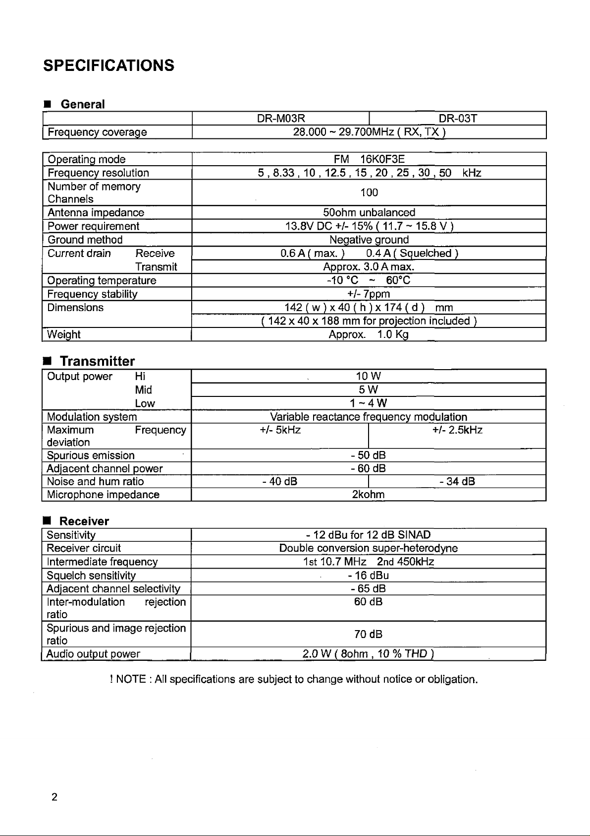
SPECIFICATIONS
■ General
DR-M03R DR-03T
Frequency coverage 28.000 ~ 29.700MHz ( RX, TX )
Operating mode FM 16K0F3E
Frequency resolution 5 , 8.33 , 10 , 12.5 , 15 , 20 , 25 , 30 , 50 kHz
Number of memory
Channels
Antenna impedance 50ohm unbalanced
Power requirement 13.8V DC +/-15% (11.7 - 15.8 V )
Ground method Negative ground
Current drain Receive
Transmit
Operating temperature
Frequency stability
Dimensions 142 ( w ) x 40 ( h ) x 174 ( d ) mm
Weight Approx. 1.0 Kg
0.6 A ( m ax.) 0.4 A ( Squelched )
Approx. 3.0 A max.
-10 °C - 60°C
( 142 x 40 x 188 mm for projection included )
100
+/- 7ppm
■ Transmitter
Output power Hi
Mid
Low
Modulation system Variable reactance frequency modulation
Maximum Frequency
deviation
Spurious emission -50 dB
Adjacent channel power
Noise and hum ratio -40 dB -3 4 dB
Microphone impedance 2kohm
+/- 5kHz
■ Receiver
Sensitivity
Receiver circuit
Intermediate frequency 1st 10.7 MHz 2nd 450kHz
Squelch sensitivity -16 dBu
Adjacent channel selectivity
Inter-modulation rejection
ratio
Spurious and image rejection
ratio
Audio output power
- 12 dBu for 12 dB SINAD
Double conversion super-heterodyne
2.0 W ( 8ohm , 1 0% T H D )
10 W
5 W
1 - 4 W
+/- 2.5kHz
-60 dB
-65 dB
60 dB
70 dB
! NOTE : All specifications are subject to change without notice or obligation.
2
Page 3
C I R C U I T D E S C R IP T I O N
1) Receiver System
The receiver system is a double super-heterodyne system with a 10.7MHz first IF and a 450kHz
second IF.
1. Front End
2. IF Circuit
3. Demodulation Circuit
The received signal at any frequency in the 28.000MHz to 29.695MHz
range is passed through the low-pass filter (L115, L114, L113, C204,
C203, C202, C216 and C215) and tuning circuit (L105 and D105), and
amplified by the RF amplifier (Q107). The signal from Q107 is then
passed through the tuning circuit {L104, L103, L102, and variable
capacitor D104, D103, D102) and converted into 10.7MHz by the mixer
(Q106). The tuning circuit, which consists of L105, variable capacitor
D105, L104, L103, L102, variable capacitor D104, D103 and D102, is
controlled by the tracking voltage from the VCO. The local signal from the
VCO is passed through the buffer (Q145), and supplied to the source of
the mixer (Q106). The radio uses the upper side of the super-heterodyne
system. .
The mixer mixes the received signal with the local signal to obtain the sum
of and difference between them. The crystal filter (XF101A, XF101B)
selects 10.7 MHz frequency from the results and eliminates the signal of
the unwanted frequencies. The first IF amplifier (Q105) then amplifies the
signal of the selected frequency.
After the signal is amplified by the first IF amplifier (Q105), it is input to
pin16 of the demodulator IC (IC108). The second local signal of 11.15MHz
(shared with PLL IC reference oscillation), which is oscillated the external
oscillator X601, is input through pin 1 of IC108. Then, these two signals
are mixed by the internal mixer in IC108 and the result is converted into
the second IF signal with a frequency of 450kHz. The second IF signal is
output from pin 3 of IC108 to the ceramic filter (FL101), where the
unwanted frequency band of that signal is eliminated, and the resulting
signal is sent back to the IC108 through pin 5. The second IF signal input
via pin 5 is demodulated by the internal limiter amplifier and quadrature
detection circuit in IC 108, and output as an audio signal through pin 9.
4. Audio Circuit
The audio signal from pin 9 of IC 108 is amplified by the audio amplifier
(IC120:A), and switched by the signal switch IC (IC111) and then input it to
the de-emphasis circuit.
And is compensated to the audio frequency characteristics in the
de-emphasis circuit (R203, R207, R213, R209, C191, C218, C217) and
amplified by the AF amplifier (IC120:B). The signal is then input to volume
(VR1). The adjusted signal is sent to the audio power amplifier (IC117)
through the pin 1 to drive the speaker.
3
Page 4
5. Squelch Circuit t
The detected output which is outputted from pin 9 of IC108 is inputted to
pin 8 of 1C108 after it was been amplified IC120:A and it is outputted from
pin 7 after the noise component was been eliminated from the composed
band pass filter in the built in amplifier of the iC, then the signal is rectified
by the internal diode in IC108 to convert into DC component. The adjusted
voltage level at VR101 is delivered to the comparator of the CPU.
The voltage is led to pin 2 of CPU and compared with the setting voltage.
The squelch will open if the input voltage is lower than the setting voltage.
During open squelch, pin 30 (SQC) of the CPU becomes “L" level, AF
control signal is begin controlled and sounds is outputted from speaker.
2) Transmitter System
1. Modulator Circuit
2. Power Amplifier Circuit
y 3. APC Circuit
The audio signal is converted to an electrical signal by the microphone,
and input it to the microphone amplifier (Q6). Amplified signal which
passes through mic-mute control IC109 is adjusted to an appropriate
mic-volume by means of mic-gain adjust VR106.
1C114:D and C consists of two operational amplifiers; one amplifier (pin
12,13 and 14) is composed of pre-emphasis and I DC circuit and the other
(pin 8, 9 and 10) is composed of a splatter filter. The maximum frequency
deviation is obtained by VR107. And input to the signal switch (IC113)
(9600 bps packet signal, input switch) and input to the anode of the
variable capacitor of the VCO, to change the electric capacity in the
oscillation circuit. This produces the frequency modulation.
The transmitted signal is oscillated by the VCO, amplified by the younger
amplifier (Q115 and Q103), and input to the final power amplifier (Q701).
The signal is then amplified by the final power amplifier (Q701) and led to
the antenna switch (D110) and low-pass filter (L113, L114, L115, C215,
C216, C202, C203 and C204), where unwanted high harmonic waves are
reduced as needed, and the resulting signal is supplied to the antenna.
Part of the transmission power from the low-pass filter is detected by
D111, converted to DC. The detection voltage is passed through the APC
circuit (IC114:B), then it controls the APC voltage supplied to final power
amplifier Q701 to fix the transmission power.
3) PLL Synthesizer Circuit
1. PLL
2. Reference Frequency
Circuit
4
The dividing ratio is obtained by sending data from CPU (1C1) to pin 10
and sending clock pulses to pin 9 of the PLL IC (IC116). The oscillated
signal from the VCO is amplified by the buffer (Q134 and Q135) and input
to pin 8 of IC116. Each programmable divider in 1C116 divides the
frequency of the input signal by N according to the frequency data, to
generate a comparison frequency of 5 or 6.25 kHz.
The reference frequency appropriate for the channel steps is obtained by
dividing the 11.15 MHz reference oscillation (X601) by 4250 or 3400,
according to the data from the CPU (IC1). When the resulting frequency is
5 kHz, channel step of 5, 8.33, 10, 15, 20, 25, 30 and 50 kHz are used.
When it is 6.25 kHz, the 12.5 kHz channel step is used.
Page 5
3. Phase Comparator Circuit
The PLL (IC116) uses the reference frequency, 5 or 6.25 kHz. The phase
comparator in the 10116 compares the phase of the frequency from the
VCO with that of the comparison frequency, 5 or 6.25 kHz, which is
obtained by the internal divider in IC116.
4. PLL Loop Filter Circuit
If a phase difference is found in the phase comparison between the
reference frequency and the VCO output frequency, the charge pump
output (pin 5) of IC116 generates a pulse signal, which is converted DC
voltage by the PLL loop filter and input to the input to the variable
capacitor of the VCO unit for oscillation frequency control.
5. VCO Circuit
AColpitts oscillation circuit driven by Q131 directly oscillates the desired
frequency. The frequency control voltage determine in the CPU (IC1) and
PLL circuit is input to the variable capacitor (D123). This change the
‘ oscillation frequency, which is amplified by the VCO buffer (Q134, Q145)
and output from the VCO area.
4) CPU and Peripheral Circuits
1. LCD Display Circuit
2. Reset and Backup
The CPU turns ON the LCD via segment and common terminals with 1/4
the duty and 1/3 the bias, at the frame frequency is 64 Hz.
When the power from the DC cable increases from Circuits 0 V to 2.5 V or
more, “H” level reset signal is output from the reset IC (IC4) to pin 33 of
the CPU (1C1), causing the CPU to reset. The reset signal , however,
waits at 100, and dose not enter the CPU until the CPU clock (X1) has
stabilized.
3. S (Signal) Meter Circuit
4. DTMF Encoder
5. Tone Encoder
6. DCS Encoder
c X601 side only.
The DC potential of IF IC is input to pin 1 of the CPU (IC1), converted from
an analog to a digital signal, and displayed as the S-meter signal on the
LCD.
The, CPU (IC1) is equipped with an internal DTMF encoder. The DTMF
signal is* output from pin 10, through R35, R34 and VR109 (for level
adjustment), and then through the microphone amplifier (1C114:D), and is
sent to the variable capacitor of the VCO for modulation. At the same time,
the monitoring tone passes through the AF circuit and is output from the
speaker.
The CPU (IC1 ) is equipped with an internal tone encoder. The tone signal
(67.0 to 250.3 Hz) is output from pin 9 of CPU to the variable capacitor
(D123) of the VCO for modulation.
The CPU (1C1 ) is equipped with an internal DCS code encoder. The code
(023 to 754) is output from pin 9 of CPU to the variable capacitor (D601) of
the PLL reference oscillator. When DCS is ON, DCS MUTE circuit
(Q126-ON, Q133-ON, Q 132-OFF) works. The modulation activates in
5
Page 6
7. CTCSS, DCS Decoder -
The voice band of the AF output signal from pin 1 of IC120:A is cut by
sharp active filter IC104:A, B and C (VCVS) and amplified, then led to pin
4 of CPU. The input signal is compared with the programmed tone
frequency code in the CPU. The squelch will open when they match.
During DCS, Q108 is ON, C419 is working and cut off frequency is
lowered.
5) Power Supply Circuit
When power supply is ON, there is a “L” signal being inputted to pin 39 (PSW) of CPU which enables the CPU to
work. Then, “H” signal is outputted from pin 41 (C5C) of CPU and drives ON the power supply switch control Q8
and Q7 which turns the 5VS ON. 5VS turns ON the PLL 1C (IC116), main power supply switch Q127 and Q122,
AF POWER IC117 and the 8V of AVR (IC115). During reception, pin 29 (R5) of CPU outputs “H" level, Q124 is ON,
and the reception circuits supplied by 8 V. While during transmission, pin 28 (T5) of CPU outputs "L” level which is
reverse by Q11 so that the output in Q128 will be “H” level, Q123 is ON, and the transmission circuit is supplied by
8 V. Or, in the case when the condition of PLL is UNLOCK, “HJ level is outputted from pin 7 of PLL IC (IC116),
UNLOCK switch Q129 is ON, transmission switch Q128 is OFF which makes the transmission to stop.
6
Page 7
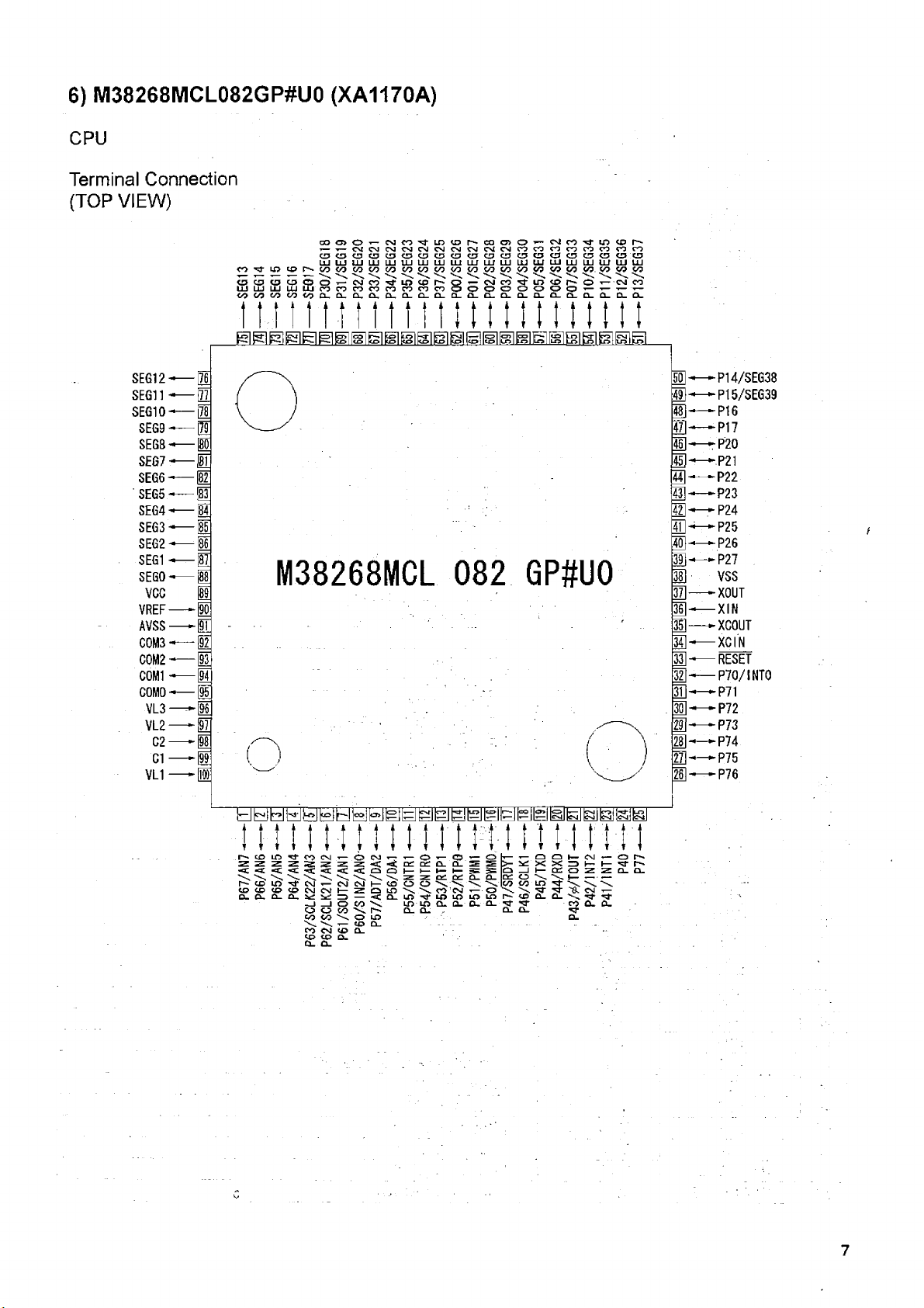
6) M38268MCL082GP#U0 (XA1170A)
CPU
Terminal Connection
(TOP VIEW)
O O O O r - C S ] n ^ L D t D f > C O O ) 0 ’" N C O ^ I i ) < O h '
T-T-C MCvlC NJC SJCS lNCS ICMC SlCvl COC OCOC OCO COO O
Q5 CD C5 C5 QTJ QTJ ^rj QTJ ^rj ^rj Q ^ 0 O ' C5
LU LU UJ LU LU UJ LLI LU LLl LU LU LU LU LU UJ LLl LU UJ LU UJ
O ü ^ y O O T - C M n ^ i O C O h - O ^ — CM ro in (O p> o 'I— cvj CO
UJ UJ LLl LU LU co c o e o e o c o c o o o c o o o o o o o o o '« — ••— ■•— ■»—
W W M W t O Q . Q . Q , Q . C L C L C L C L Q _ C L a . Q . Q . O . D - D _ Q . Q . C L Q .
W(OWWCOWWWCQCQCOW(/5WWWW.WWtO
y i n f i n m n t m i m n
SI Él Él É] El ^1 HI SI É 1 EH Esl SI Él Él É1 111 Isl Él É l É l SI SI É l Él Él
SE612-
SEG11■
SEG10-
SEG9-
SEG8-
SEG7
SEG6-
SEG5 ■
SEG4-
SEG3-
SEG2-
SEG1 ■
SEG0-
VCC
VREF-
AVSS
COM3'
COM2-
C0M1 ■
COMO
VL3 ■
VL2-
C2
C1-
VL1-
i i i i-t- n u
r-
CO in
z z z z
'C
-c
N \
N
r-COur>
<o
CO CO CO
£Xn_n.
CL
,—
co
Cvj
CM CM1—zQto \
_
o o00\
S'*
CO CslCOQ_
to to
Q_
1
Z
<c <c
_l
CO
O-
O
< O
\
CM 1—
CM
oCO\
\
o
CO
Q_
CM
<C Q¿ a i
<C
o J—
\
CO oo\
Q_
C
to
Q_
,—
LO ■sr
LO
Q_ Q.
o
Q_ Q-
i—
*—
cd CÉ
CO CM
LO LO
IO Q. Q.
*—
O
S
a.
\
LO
O,
Page 8
No. Terminal
1 P67/AN7
2
3 P65/AN5
4 P64/AN4
5 P63/SCLK22/AN3
6 P62/SCLK21/AN2
7
8 P60/SIN2/AN0
9 P57/ADT/DA2
10 P56/DA1
11 P55/CNTR1
12
13 P53/RTP1
14 P52/RTP0
15 P51/PWM1 CLK o Serial clock output for PLL
. 16 P50/PWMO
17
18 P46/SCLK1 STB 0
19 P45/TXD
20 P44/RXD
21 P43M/TOUT
22 P42/INT2
23 P41/INT1
24 P40
25 P77
26 P76 SSTB O Security mode
27
28
29
30 P72
31 P71
32 P70/INT0
33 RESET RESET f Reset input
34 XCIN Xcin
35 XCOUT Xcout
36 XIN Xin - 7 Main clock input
37
38 VSS GND
39 P27 PSW I
40 P26 SDA O Serial data for EEPROM
41 P25 CSC o
42
43 P23 LOW o Tx low power
44 P22
45 P21
46
47
48 P16
49 P15/SEG39 SW2 I Key sw 2 (V/M)
50 P14/SEG38
P66/AN6
P61/SOUT2/AN1
P54/CNTR0 TBST o Tone burst output
P47/SRDY1 TSTB I/O Trunking board detection / Strobe signal to trunking board
P75 W/N o
P74 T5 0
P73 R5 0
XOUT Xout
P24 MID o Tx middle power
P20 SW5 I
P17 SW4 I Key sw 4 (TSQ)
Signal I/O
SMT I
SQL
BP5
TIN I
r~ b p i
BP2
DCSW
RE2
TOUT
DOUT
SCL
BP4 I/O
MUTE I/O
DATA I/O
UTX
RTX I
BEEP
SEC
RE1
PTT
SQC
BU
EXP
SW6
SW3
SW1
S-meter input
I Noise level input for squelch
I Band plan 5
CTCSS tone input / DCS code input
Band plan 1
I
Band plan 2
I
0 DCS signal mute
I Rotary encoder input
0
CTCSS tone output / DCS tone output
o DTMF output
o
Serial clock for EEPROM
Band plan 4
Microphone mute / Security alarm SW
Serial data output for PLL / PLL unlock signal input
Strobe for PLL IC
o
I/O
.. -
UART data transmission output
UART data reception output
Beep tone / Band plan 3
I
Security voltage input
I Rotary encoder input
I PTT input
Wide Narrow SW
TX power ON / OFF output
RX power ON / OFF output
0 SQL ON/OFF
I
Backup signal detection input
-
-
-
Main clock output
-
CPU GND
Power switch input
C5V power ON / OFF output
0
Trunking / Packet data SW
I
Key sw 6 (SQL)
Key sw 5 (CALL)
I
Key sw 3 (MHz)
I
Key sw 1 (FUNC)
Description
8
Page 9
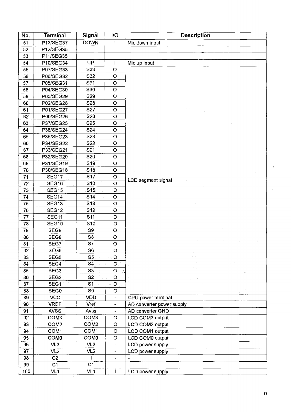
No. Terminal
51 P13/SEG 37 DOWN I
52
53
54 P10/SEG 34
55 P07/SEG 33
56 P06/SEG32 S32
57 P05/SEG31
58 P04/SEG 30
59 P03/SEG 29
60 P02/SEG 28
61 P01/SEG 27
62
63 P37/SEG 25
64 P36/S E G 24
65 P35/SEG 23 S23 0
66
67 P33/SE G 21
68 P32/SEG 20 S20 o
69 P31/SEG 19 S19 0
70 P30/SEG18 S18 0
71
72
73 S E G 15 S15 0
74 SEG 14
75 S E G 13 S13 o
76 S E G 12 S12 o
77
78 S E G 10 S10 0
79 SEG9
80 S E G 8
81 S E G 7
82
83 S EG 5
84 S E G 4
85 S E G 3
86 S E G 2
87
88 SEGO
89 VCC VDD
90
91 A VSS
92
93
94 COM1 COM1
95 COMO COMO
96 VL3 VL3
97
98
99 C1
100
P12/SEG 36
P11/SEG35
P00/SEG 26 S26 0
P34/SEG 22 S22
SEG17
SEG16
SEG11 S11
•SEG6
SEG 1
VREF
COM 3 C O M 3 o
COM 2
VL2
C2
VL1 VL1 I
Signal I/O Description
UP I
S33
S31 0
S30 0
S29
S28
S27
S25
S24 o
S21 0
S17
S16
S14 0
S9
S8 o
S7
S6
S5 o
S4
S3 o A
S2
S1
SO
Vref
Avss
COM 2 0
VL2
I
C1
Mic down input
Mic up input
0
o
0
o
0
o
0
o
LCD segment signal
o
o
0
o
0
o
0
o
o
-
CPU power terminal
-
AD converter power supply
-
AD converter GND
LCD C O M3 output
LCD C OM 2 output
o
o
LCD COM1 output
LCD COMO output
-
LCD power supply
-
LCD power supply
- -
-
-
LCD pow er supply
9
Page 10
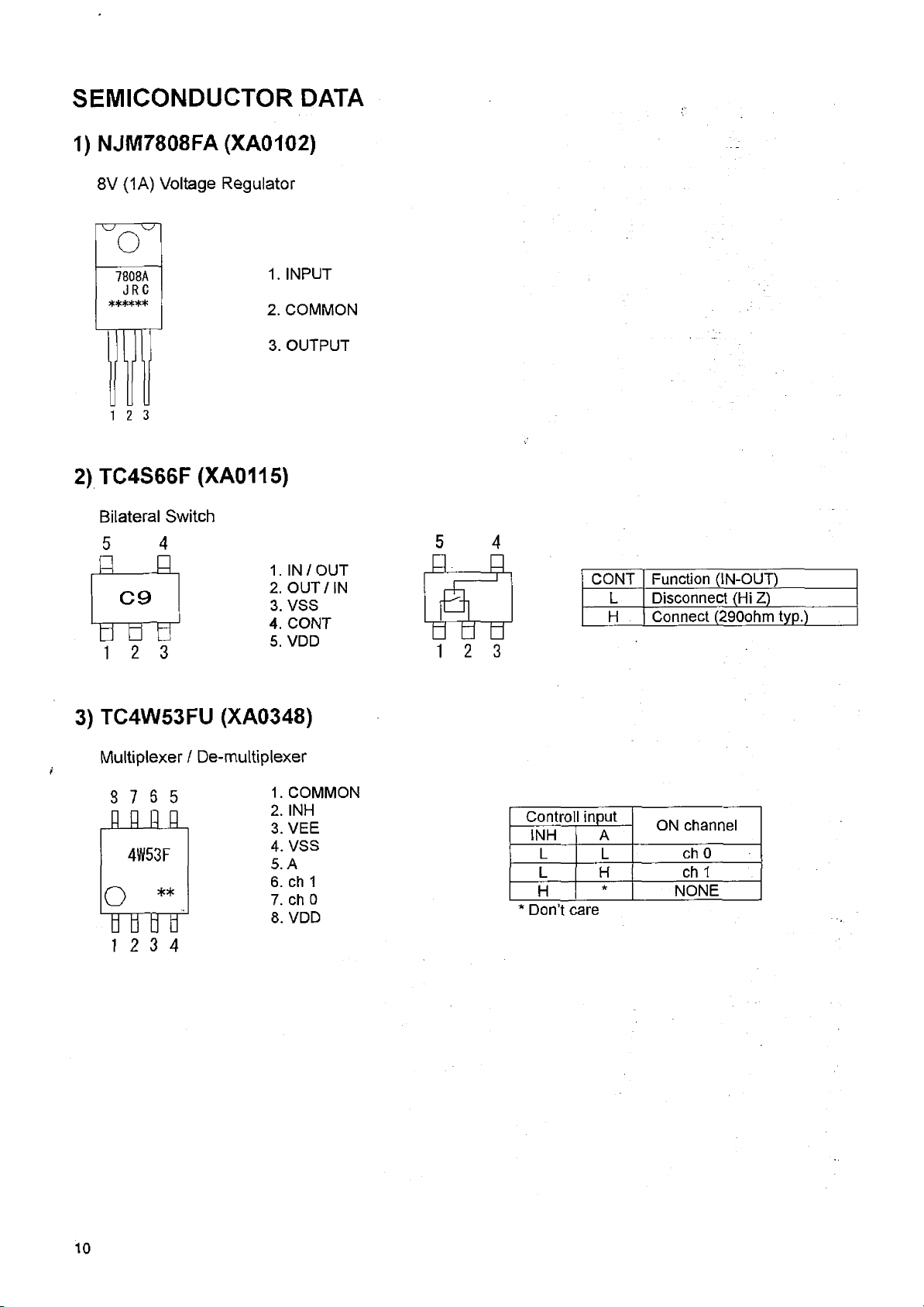
S E M IC O N D U C T O R D A T A
1) NJM7808FA (XA0102)
8V (1A) Voltage Regulator
1. INPUT
2. COMMON
3. OUTPUT
1 2 3
2) TC4S66F (XA0115)
Bilateral Switch
5 4
s
____
a
C9
d d d
1 2 3
1. IN/OU T
2. OUT/IN
3. VSS
4. CONT
5. VDD
5
BL f l
M
d a d
1 2 3
CONT
Function (IN-OUT)
L Disconnect (Hi Z)
H Connect (290ohm typ.)
3) TC4W53FU (XA0348)
Multiplexer / De-multiplexer
8 7 6 5
n nil a.
m i
12 3 4
1. COMMON
2. INH
3. VEE
4. VSS
5. A
6. ch 1
7. ch 0
8. VDD
Control
INH
L
L
H
Don’t care
input
A
L
H ch 1
*
ON channel
ch 0
NONE
10
Page 11
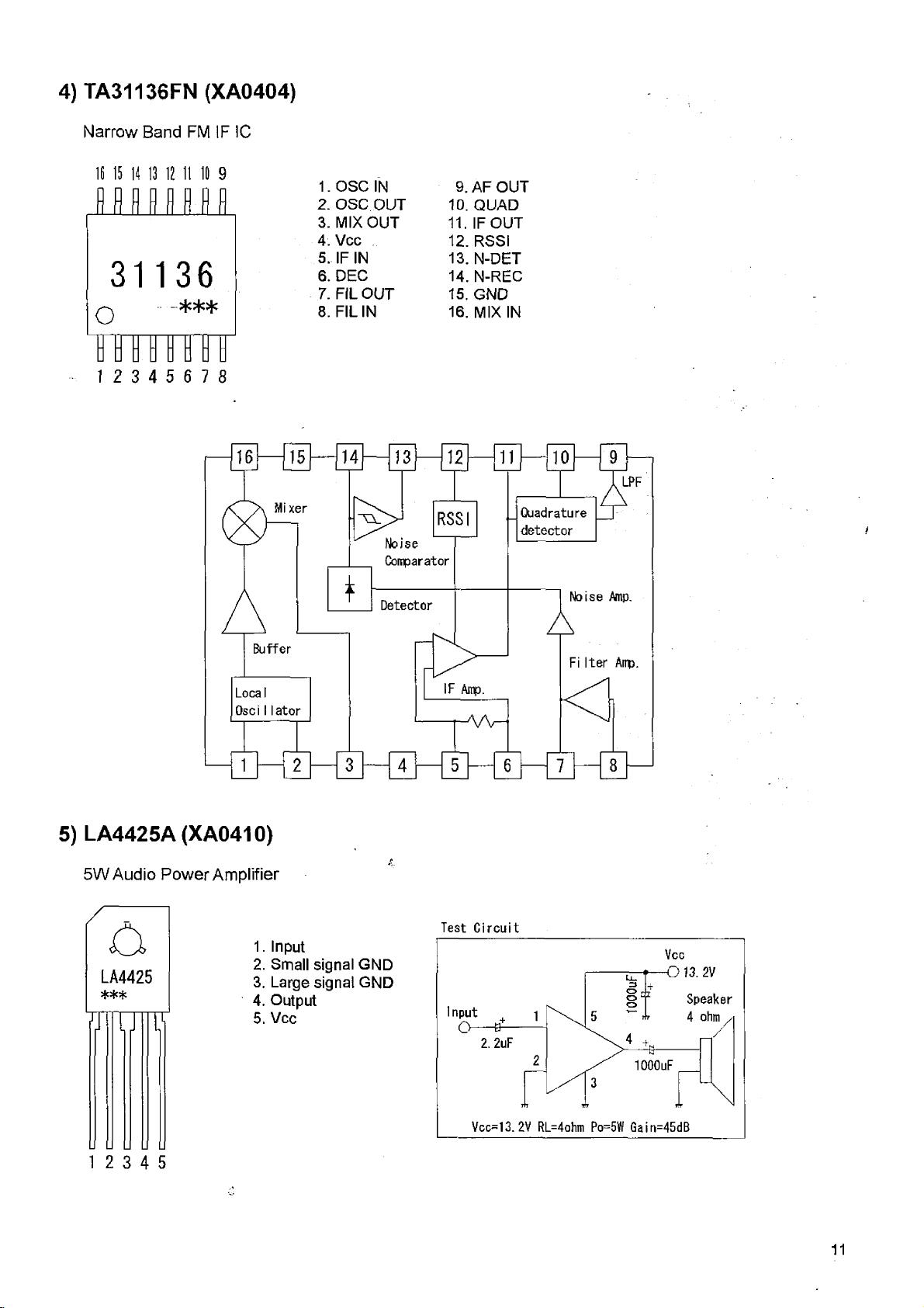
4) TA31136FN (XA0404)
Narrow Band FM IF IC
16 15 14 13 12 11 10 9
flflflflyn
0
n u m i
1 2 3 4 5 6 7 8
1. OSCIN
2. OSC OUT
3. MIX OUT
4 . Vcc
5. IF IN
6. DEC
7. FIL OUT
8. FILIN
9.AF OUT
10. QUAD
11. IF OUT
12. RSSI
13. N-DET
14. N-REC
15. GND
16. MIX IN
5) LA4425A (XA0410)
5W Audio Power Amplifier
Ö .
LA4425
***
12 3 4 5
1. Input
2. Small signal GND
3. Large signal GND
4. Output
5. Vcc
Test Circuit
11
Page 12

6) BR24L32FJ (XA0604Z)
32K-Bit EEPROM
8 7 6 5
R -ELELFL
F ¥ ¥ ¥
1. AO
2. A1
3.A2
4. Vss
5. SDA
6. SCL
7. WP
8. Vcc
1 2 3 4
7) S-80845ALMP (XA0620)
4.5V Voltage Detector
4
P
B 6 6*
n b t i '
1. GND
2. Vin
3. Vout
4. NC
5. NC
1 2 3
8) NJM78M05DL1A (XA0947)
Name
A0...A2
Vss
SDA
SCL
WP
Vcc
Function
User Configurable Chip Select
Ground
Serial Address / Data / I/O
Serial Clock
Write Protect Input
+2.5 ~ 6.0V Power Supply
5V (500mA) Voltage Regulator
r i
7 8 M 0 5 A
o
1. input
2. GND
3. Output
i zr ^
2
—
1 3
—
12
Page 13

9) MB15A01PFV1 (XA1010)
PLL Synthesizer
1 6 1 5 1 4 13 1 2 1 1 10 9
15A01
***
o
u rn
1 2 3 4 5 6 7 8
1. OSCIN
2. OSC OUT
3. Vp
4. Vcc
5. Do
6. GND 14. fout
7. LD
8. fin
9. Clock
10. Data
11. LE
12. FC
13. N. C.
15. 4>P
16. 0R
Parameter
Power supply voltage Vcc
Power supply current
LPF supply voltage
Local oscillator input level Vfin
Local oscillator input
frequency
Xin input level
Xin input frequency Fxin
Symbo
I
Icc
Vp
fin
Vxin
( Vcc = 2.7 to 3.5V, Ta = -40°C to +85°C )
Condition Min. Typ. Max. Unit
-
2500MHz
Vcc=Vp=3.75V
-
-
-
2.7 3.0 3.5 V
6.5 mA
Vcc
-10
10 1100 MHz
*
0.5
-
-
12 23 MHz
6.0
+6 dBm
-
V
Vp-p
13
Page 14

10) LM2904PWR (XA1103)
Dual Operational Amplifiers
8 7 6 5
1. Output A
2. Inverting Input A
3. Non-inverting Input A
4. GND
5. Non-inverting Input B
6. Inverting Input B
7. Output B
8. Vcc
12 3 4
11) LM2902PWR (XA1106)
Quad Operational Amplifiers
1413121110 9
8
1. Output A
2. Inverting Input A
3. Non-inverting Input A
4. Vcc
5. Non-inverting Input B
6. Inverting Input B
7. Output B
8. Output C
9. Inverting input C
10. Non-inverting Input C
11. GND
12. Non-inverting Input D
13. Inverting Input D
14. Output D
12) TA78DS10F (XA1249)
10V (30mA) Voltage Regulator
( I
1. OUTPUT
2. COMMON
Tnrrr
1 2 3
3. INPUT
14
Page 15

13) Transistor, Diode and LED Outline Drawing
Top View
Ml 407
XDÖÖ13
1SS383
XDÓ426
2SK2_539
XÉÓÓ66”
G
XL
AK*
DA204U 1SV268
XD0130 XD0320 XD0380 XD0402 XD0414
K
n— u
r i
I I — CJ
JDV2S14
XD0427
XDÖ301
H L
u m r
i—i
f t
1SS383
XDÖ461
n n
A4
D Q
n. _n
n ~ n
FA1111C
FA11J1C
' XLÓÓ77'
DAN235E
V----IT
_□
_
H r
1SS406
XDÓ462
[fA7>
2SC3356T1
" XT003Ö"
SVC347S
f t
2SK880GR
XËÔ62Î"
XG
2SA1576A
~xfÓÓ94"
R24 FR
I] U
B E
VDZ5. 1B
iEEî
2SK3074
"XEÖÖ44”
WA
U Ü U
G S D
2SC408Í
xf0095
C
n
BR
S3V60
J ~ L
3SK293
XE0053
G2 ~G1
j
___
UF
b— n
D S
2SC4915
XT0178 ~XL0069
c
n
Q0
n — u
B E
a
2SB1386
xf0190
Jin
BHQ
~n—n rr
B C É
RN1711
XÚÓ226
t_> o
u m i
Rb=10kohm
Rbe=none
2SA2070
XT0223 "
JHZL
4SI C
¡J I I I !
B C Ê
2SC4738
' XTÖ224'
LG
RN1104
XU0195
XD
in— u
Rb-47kobm
Rbe=47kohm
EMD
6
XÚÓ2Ó9
Rb=4.7kohm
Rbe=none
RN1107FV
XÜÓ21Ó
XH
TT~[T
E E
Rb=1Qkohm
Rbe=47kohm
RN2107FV
XÛ0211 "
Rb=10kohra
Rbe=47kohm
Page 16

14) RD16HHF1 (XE0056)
Nch MOS FET
O U T L I N E D R A W IN G
PIN
© GATE
(2) SOURCE
® DRAIN
<D FIN (SOURCE)
9.5m
ABSOLUTE MAXIMUM RATING ( Tc = 25°C, unless otherwise noted )
Symbol Parameter
VDSS Drain to source voltage
VGSS
Pch Channel dissipation
Pin Input Power
ID
Tch
Tstg Storage temperature
Rth j-c
Gate to source voltage
Drain to source Current
Channel temperature
Thermal resistance Junction to case 2.2
5
CO
ii
Vds = OV
Tc = 25 °C
Zg = Zl = 50 Q
>
0
-
-
-
Conditions
ELECTRICAL CHARACTERISTICS ( Tc = 25 °C, unless otherwise noted )
Symbol
loss
Igss
Vth
Pout Output Power
n D
Zero gate voltage drain current
Gate to source leak current
Gate threshold voltage
Drain Efficiency
Load VSWR Tolerance
Parameter Conditions
VDs =17V,VGs =0V
VGS = 10V,VDS = 0V
Vos = 12V, Ids = 1mA
f= 30MHz, Vqd = 12.5V
Pin = 0.4W, ldq=0.5A
VDD = 15.2V, P0 = 16W (Pin Control)
f = 30MHz, Jdq = 0.5A, Zg = 50 ß
Load VSWR = 20:1 (ALL Phase)
Ratings Unit
50 V
+/-.20
56.8 W
0.8 W
5 A
150 °C
' -40 to+150 °C
°c/w .
Limits
Typ
Min
-
- -
1.7
16 19
55 65 -
No degradation
-
Max
10
1
7.7 V
-
V
Unit
ß A
/i A
W
%
16
Page 17

\
Page 18

15) LCD Connection (TTR3626UPFDHN)
Page 19

2) Top and Front View
AA 0050
18
NK0073
Page 20

3) Bottom View
' AA0050
Page 21

EXPLODED VIEW
1) LCD Assembly
FF0017
20
Page 22

PARTS LIST
CPU Unit
Ref No
Part No.
C l
CU3554
C2
CU3554 Chip C. GRM155B11A104KA01D
C3
CU3549 Chip C.
C4
CU3549
C5
CU3554 ChipC.
C6
CU3523 Chip C.
C7
CU3523
08
CU3543
C9
CU3554 Chip C,
C10
CU3543 ChipC.
C11
CU3543
C12
CU3553
C13
CS0049 Chip tantalum
C14
CU3514
C15
CU3514 Chip C.
C16
CU3535 Chip C.
C17
CS0424
C18
CU3535
C19
CU3554 Chip C.
C20
CU3547 Chip C.
C21
CU3547
CU3535
C22
C23
CU3547 Chip C. G RM155B11C103KA01D
C24
CU3535 Chip C.
C25
CU3535 Chip C.
C26
CU3535 Chip C. GRM155B11H102KA01D
C27
CU3535 Chip C.
CN1
UE0291
CN2
UE0291 Connector
CN3
UE0035Z
D1
XL0069
02 XL0077
D3
XL0077 Chip LED
D4
XL0069 Chip LED FA1111C-TR
D5
XL0077 Chip LED
D6
XL0077 Chip LED
D8
XD0426
D9
XD0462 Chip Diode
D11
XL0077 : Chip LED
017
XD0462
IC1
XA1170A
IC2
XA0604Z
IC4
XA0620 1C
ICS
XA0348
JK1
UJ0047
JP3
MACL04GG
LCD1
EL0049 LCD
Q4
XU0210
Q6
XT009S
Q7
XT0223 Chip
Q8
XU0210 Chip
Q10
XU0210 Chip
Q11
XL) 0211 Chip
Q12
XU0211 Chip
R1
RK3S54 Chip R.
R4
RK3554 Chip R.
R5
RK3550
R6
RK3550 Chip R.
R7
RK3026 Chip R.
RK3026
R8
R10
RK3032 Chip R.
R11
RK3546 Chip R ..
RK354B
R14
R19
RK3562 Chip R.
R20
RK3546 Chip R.
RK3538
R22
R25
RK3S50
R26
RK3550 Chip R.
RK3550
R27
R28
RK3538
R29
RK3538 Chip R.
R30
RK3538 Chip R.
RK3544
R32
R33
RK3534
R34
RK3547 Chip R.
R35
RK3552
R36
RK3562
R37
RK3549 Chip R.
R38
RK3551
RK3558
R39
R40
RK3562
R41
RK3526 . Chip R.
R42
RK3550 . Chip R.
R43
RK35S0 ;
R44
RK3026 Chip R.
R45
RK3550
Description Parts Name
Chip C.
Chip C. GRM155B11C153KA01D
Chip C. G RM1552C1H101JD01D
Chip C.
Chip C. G RM155B11H392KA01D
Chip C.
Chip C. GRM1552C1H180JZ01D 1 1
Chip tantalum
Chip C. GRM1S5B11H102KA01D
Chip C. GRM155B11C103KA01D 1
Chip C. GRM155B11H102KA01D
Connector
Mic Connector MIC FM214-8SMPY(Z) 1 1
Chip LED FA1111C-TR
Chip LED
Chip Diode
Chip Diode
1C
1C
1C
Jack
Wire
Chip
Chip
Chip R.
Chip R.
Chip R.
ChipR. .
Chip R.
Chip R.
Chip R.
Chip R.
Chip R.
Chip R.
Chip R.
CJitp R. ERJ2GEJ123X
Chip R.
Chip R.
Chip R.
Chip R.
GRM155B11A104KA01D
GRM155B11C153KA01D
GRM155B11A104KA01D
GRM1552C1H101JD01D 1 1
G RM155B11H392KA01D 1 1
GRM155B11A104KA01D
GRM155 B11H392KA01D 1 1
GRM155B11A473KA01D
TMCSA1C105MTRF
G RM1S52C1H180 J201D 1
GRM155B11H102KA01D
TMCMA1C106MTRF
GRM155B11A104KA01D
GRM155B11C103KA01D
GRM155B11H102KA01D 1
GRM155B11H102KA01D 1
G RM155B11H102KAD1D 1 1
17R-JE(LF)(SN)
t7R-JE(LF)(SN]
FA1111C-732-TR
FA1111C-732-TR 1
FA1111C-732-TR 1
FA1111C-732-TR 1
1SS387
1SS406(TPH3,F) 1 1
FA1111C-732-TR 1
1SS406(TPH3,F) 1
M38268MCA-082G P#UO
BR24L32FJ-WE2 1 1
S80845CLMC-B66-T2G
TC4W53FUCTE12L)
HSJ2013-01 -120
#30 AH1-040-H1
LCD DR13S 1 1
RN1107MFV{TPL3) 1
2SC4081 T106R
2SA2070(TE12L,F) 1 1
RN1107MFV{TPL3)
RN1107MFV(TPL3)
RN2107MFV(TPL3)
RN2107MFVfTPL3)
ERJ2GEJ223X 1 1
ERJ2GEJ223X
ERJ2GEJ103X
ERJ2GEJ103X 1
MCRD3EZPJ101 1 1
MCR03EZPJ101
MCR03EZPJ331 1 1
ERJ2GEJ472X 1
ERJ2GEJ682X
ERJ2GEJ104X 1 1
ERJ2GEJ472X 1 1
ERJ2GEJ102X
ERJ2GEJ103X
ERJ2GEJ103X 1
ERJ2GEJ103X 1
ERJ2GEJ102X
ERJ2GEJ102X 1 1
ERJ2GEJ102X 1
ERJ2GEJ332X 1
ERJ2GEJ471X 1
ERJ2GEJ562X 1
ERJ2GEJ153X 1
ERJ2GEJ104X 1
ERJ2GEJ822X 1 1
ERJ2GEJ473X
ERJ2GEJ104X
ERJ2GEJ101X
ERJ2GEJ103X
ERJ2GEJ103X
MCR03EZPJ101 1
ERJ2GEJ103X
DR-M03R
1
1 1
1
1 1
1
1
1
1
1 1
1
1
1 1
1
1
1
1 1
1
1
1
1 1
1 1
1
1 1
1
1 1
1 1
1
1
1
1 1
1
1
1
1
1
1
1 1
1
1 1
1
1
Qty.
DR-03T
1
1
1
1
1
1
1
1
1
1
1
1
1
1
1
1
1
1
1
1
Part No.
Ref No.
RK3538
R4S
RK3570
R50
R51 RK3538
R52 RK3538
RK3562
R53
R54 RK3550
RK3S74
RSS
R56 RK3550
RK3566 Chip R.
R57
RK3534
R58
RK3526
R59
RK3034 Chip R.
R60
R61 RK3574
R52 RK3550
R63 RK3526 Chip R.
R64 RK3549
R65 RK3525
RK3550 Chip R.
R66 .
R67 RK3526 Chip R.
R63 RK3550
Rfâ562 Chip R,
R70
RK3574
R71
R72 RK3550
R73 RK3032
R74 RK3526
R76 RK3532
RK3538 Chip R.
R79
RK3538 Chip R.
R80
R85 RK3546
RK3554 Chip R.
R87
RK3550
R88
RB9 RK3558
RK3558 Chip R.
RSO
R98 RK3501
RE1 LIR0015
UU0042 Switch
SW1
SW2 UU0042 Switch
SW3 UU0042 Switch
SW4 UU0042 : Switch
SW5 UU0042 Switch
SW6 UU0042 Switch
UU0042 Switch
SW7
VR1 RV0035 Variable R.
X1 XQ0131
DG0037 : LCD LIGHT DR135
FF0017
FG0305
FM0034 MICGND PLATE
FP0034
FP0234
ST0064
ST0068 DIAL FITTING DR135
TL0023
TL0024 DIFFUSION SHEET 135
Y20042
N Uni
MA
Ref No. Part No.
CU353S
C101
C103
CU3535
CU3047 ChipC .
C104
C105 CS0439
C107 CU3S54
C108 CU3547
CE0339
C109
C110 CU3547
CU3554 Chip C.
c m
CU3554 Chip C.
C112
C113 CU3047
C114 CU3547
CU3003 Chip C.
C115
C116
CU3019
C117 CU3547
C120 CU3522
CU3504 Chip C.
C122
C123 CU3513
C129 CU3547
CU0108
C130
C132 CU3535
C135 CU3547
C136 CU3011 Chip C.
C137 CU3517
C139 CU3535
Description Parts Name
Chip R.
Chip R.
Chip R.
Chip R. ERJ2GEJ102X
Chip R.
Chip R. ERJ2GEJ103X
Chip R.
Chip R.
Chip R.
Chip R.
Chip R.
Chip R.
Chip R.
Chip R,
Chip R.
Chip R.
Chip R.
Chip R.
Chip R.
Chip R.
Chip R.
Chip R.
Chip R.
Chip R.
Dial
Xtal
Cloth BLIND CLOTH DR570
Description
Chip C.
Chip C.
Chip tantalum
Chip C.
Chip C.
Electrolytic C.
Chip C.
Chip C.
Chip C.
Chip C.
Chip C.
Chip C.
Chip C.
Chip C.
Chip C. LMK212BJ105KG-T
Chip C.
Chip C.
Chip C.
Chip C.
ERJ2GEJ102X 1
ERJ2GEJ474X 1 1
ERJ2GEJ102X 1 1
ERJ2GEJ104X 1 1
ERJ2GEJ105X
ERJ2GEJ103X
ERJ2GEJ224X 1 1
ERJ2GEJ471X
ERJ2GEJ101X
MCR03EZPJ471 1
ERJ2GEJ10SX 1 1
ERJ2GEJ103X 1 1
ERJ2GEJ1Q1X
ERJ2GEJ822X 1 1
ERJ2GEJ101X 1 1
ERJ2GEJ103X
ERJ2GEJ101X 1 1
ERJ2GEJ103X 1 1
ERJ2GEJ104X
ERJ2GEJ105X 1 1
ERJ2GEJ103X 1 1
MCR03EZPJ331
ERJ2GEJ101X
ERJ2GEJ331X 1 1
ERJ2GEJ102X
ERJ2GEJ102X 1 1
ERJ2GEJ472X 1 1
ERJ2GEJ223X
ERJ2GEJ103X 1
ERJ2GEJ473X 1 1
ERJ2GEJ473X
ERJ2GEOROOX 1 1
RH90N74E20-A90770
SKQYAAE010
SKQYAAE010 1 1
SKQYAAE010
SKQYAAE010
SKQYAAE010 1 1
SKQYAAE010
SKQYAAE010
EVUF2JFK4B14 1 1
CSA310 3.686400MHZ
LCD RUB.CONNECT. 13S 1 1
MIC SPACER DR110 1 1
MIC SPACER A DR135
LCD HOLDER DR135
REFLECTION DR135 1
CEMENT G17/1G
GRM1S5B11H102KA01D
G RM155B11H102KA01D
C1608JB1H103KT-NS
TMCMA0J476MTRF
GRM155B11A104KA01D
G RM155B11C103KA01D
16ME10SWB+TS-ALC
GRM155B11C103KA01D
GRM155B11A104KA01D
GRM1S5B11A104KA01D
C1608JB1H103KT-NS
GRM155B11C103KA01D
C1608CH1H020CT-NS I
C1608CH1H470JT-NS
G R Ml 55B11C103KA01D
GRM1552C1H820JD01D
GRM1553C1H3R0CZ01D
G RM1552C1H150JZ01D
G RM155B11C103KA01D
GRM1S5B11H102KA01D
G RM155B11C103KA01D
C1608CH1H100DT-NS L
GRM1552C1H33ÛJZ01D
GRM155B11H102KA01D
Qtv.
DR-M03R
1 1
1 1
t
1
1
1 1
1 1
■J
1
1 1
1 1
1
1 1
1 1
1
1
1
1 1
1
1
1
1
1
1
1 1
1 1
1 1
Parts Name Qty.
□R-03T
i
1
1
1
1
1
1
1
1
1
1
1
t
1
1
1
1
1
1
1
1
t
21
Page 23

Part No.
Ref No.
C140
CU3535
C143
CU3554 Chip C.
C144
CU3535 Chip C. GRM155B11H102KA01D
C145
CU3523 Chip C. GRM1552C1H101JD01D
C146
CE0364
C148
CU3535 Chip C. GRM1S5B11H102KA01D
C149 CU3535 Chip C. GRM155B11H102KA01D
C151 CU3535 Chip C. GRM155B11H102KA01D
C152 CE0339 Electrolytic C.
C154
CU3535 Chip C. GRM155B11H102KA01D
C155 CU3505 Chip C. GRM1552C1H4R0CZ01D
C157 CU3535 Chip C.
C158
CU3535 Chip C.
C159 CU3511
C161
CU3535
C163 CU3535 Chip C. GRM155B11H102KA01D
C164
CU3535 Chip C. GRM155B11H102KA01D
C16S
CU3559
C166 CE0420 Electrolytic C. 16ME22SZ
C169
CU3527 Chip C. GRM1552C1E221JD01D
C170
CU3554
C173 CU3537 Chip C.
C174 CU3527 Chip C. G RM1552C1E221JD01D
C175
CU3535 Chip C.
C177
CU3035
C178 CU3047 Chip C. C1608JB1H1D3KT-NS
C179 CU3554 Chip C. GRM155B11A104KA01D
C180
CU3535
C182 CU3535 Chip C. GRM155B11H102KA01D
C183
CU3023 Chip C.
C184
CK0002
C185 CS0232 Chip tantalum TMCMA1V474MTRF
C186
CU3535 Chip C. GRM155B11H102KA01D
C187
CU3535
C188 CU3535 Chip C. GRM155B11H102KA01D
C189 CU3523 Chip C. GRM1552C1H1G1JD01D
C190
CU3547
C191 CU3552 Chip C. GRM155B11A333KA01D
C193 CK0002
C196 CU3523
C199 CE0339 Electrolytic C. 16ME1 OSWB+TS-ALC
C200
CU3035 ChipC. C1608JB1H102KT-NS
C201 CU4019 Chip C.
C202 CU9037 Chip C. C3216CH2J181 JT
C203
CU9036
C204 CU4020 Chip C.
C205 CU3035 Chip C. C1608JB1H102KT- N S
C20S CE0339 Electrolytic C.
C207 CU3003 Chip C.
C208 CU3001 Chip C.
C209
CU3547
C210 CU3006 Chip C. C1608CH1H050CT-NS
C211 CU3006 Chip C. C1608CH1H050CT-NS
C212
CE0364
C213 CU3035 ChipC. C1608JB1H102KT-NS
C214
CU3535 ChipC. GRM155B11H102KA01D
C215
CU4025
C216 CU903t) Chip C. C3216CH2J151 JT
C217 CU3551 ;
C218
CU3551
C219 CÜ3035 Chip C. C1608JB1H102KT-NS
C220
CU3035 Chip C.
C224
CU3023
C225 CU3035 Chip C.
C226
CU3035
C227 CU0108 , Chip C. LMK212BJ105KG-T
C228 CU3535 Chip C. G RM155B11 H I 02KA01D
C229 CU3553-
C230
CU3535
C231 CU3535 Chip C. GRM155B11H102KA01D
C232
CU3S35 ;
C233
CU3535 :
C235 CU3523 Chip C. GRM1552C1H101JD01D
C236
CU3S23 Chip C. GRM1552C1H101JD01D
C237 CU3535 ChipC.
C238
CU3554 Chip C. GRM15SB11A104KA01D
C239
CU3535 Chip C.
C241
CU3522
C242 CU3551 Chip C.
C243 CE0339 : Electrolytic C,
C244
CE0339
C245 CS0237 Chip tantalum TMCMA1A475MTRF
C246 CU3543 Chip C.
C248
CU3547
C249 CU3538 Chip C.
C250 CU3526
C253
CU3551
C254 CU3059 ChipC.
C255 CED364
C256
CU3059 ’
C257 CE0339
Description Parts Name
Chip C. GRM155B11H102KA01D
Electrolytic C. 16ME47SWB+TS
Chip C. GRM1552C1H100JZ01D
Chip C.
Chip C, G RM155B30J105KE18D
Chip C. GRM155B11A104KA01D
ChipC .
Chip C.
Ceramic C.
Chip C.
Chip C.
Ceramic C.
Chip C.
Chip C.
Chip C.
Electrolytic C.
Chip C.
Chip C. GRM155B11C223KA01D
Chip C. G RM155B11C223KA01D
Chip C. C1608CH1H101 JT-NS
Chip C.
Chip C.
Chip C.
ChipC .
Chip C.
Chip C. . ... G RM1552C1H820JD01D
Electrolytic C.
Chip C,
ChipC .
Chip C.
Electrolytic C.
Chip C.
Electrolytic C.
GRM155B11A104KA01D
16ME1OSWB+TS-ALC
G RM155B11H102KA01D
GRM155B11H102KA01D
GRM155B11H102KA01D
GRM155B11H152KA01D
G RM155B11H102KA01D
C1608JB1H102KT-NS
GRM155B11H102KA01D
C160BCH1H101JT-NS
HE60SJVF103Z
GRM155B11H102KA01D
GRM155B11C103KA01D
HE60SJYF103Z
GRM1552C1H101JD01D
GRM31M2C2H470JV01L
C3216CH2J151JT
GRM31M2C2H560JV01L
16ME1 OSWB+TS-ALC
C1608CH1H020CT-NS
C1608CH1HDR5CT-NS :
GRM155B11C103KA01D
16ME47SWB+TS
G RM31MR72H221KY21L
C1608JB1H102KT-NS
C1608JB1H102KT-NS
C1608JB1H102KT-NS
GRM155B11A473KA01D
GRM155B11H102KAÛ1D
GRM155B11H102KA01D
GRM155B11H1Q2KA01D
GRM155B11H102KA01D
GRM155B11H102KA01D
G RM155B11C223KA01D
16ME1 OSWB+TS-ALC
16ME1 OSWB+TS-ALC
GRM155B11H392KA01D
G RM155B11C103KA01D
GRM155B11H182KA01D
GRM1552C1E181JD01D
G RM155B11C223KA01D
C1608JF1H104ZT-NS ,
16 M E47 SWB+T S
C1608JF1H104ZT-NS
16ME1 OSWB+TS-ALC
Qty.
' 1
- 1
Part No. Description
Ref No.
1
1
1
1
1
1
1
1
1
1
1
1
1
1
1
1
1
1
1
1
1
1
1
1
1
1
1
1,
1
1
1
1
1
1
1
1
1
1
1
1
1
1
1
1
1
CU 0108
C258
C260 CE0339
C261 CU3535 Chip C.
C262 CU3535 -
C263
CS0424
C264 CU3531
C268 CU3535
C269 CU3535
C270 CU3047 Chip C.
CS0237
C272
C273
CS0237 Chip tantalum
C274
CU3535
C275
CU3547 Chip C.
C276 CS0220
C277 CE0343
CU3535
C278
C279 CU3547
C281 CU3543
C282 CU3511
C283 CU3547
C284 CU3543
C285 CU3535
C286 CU3027 ChipC. C1608CH1H221 JT-NS
CS0235
C287
C289 CU3535
CU3535
C290
CU3535
C293
C294 CU3035 .
CU3535
C297
C300
CU3527
C301 CU3523
C302 CU3523
C303 CU3523
C305 CU3547
C306 CU3554
C307 CU3547
C308 CE0353
C309 CU3551 Chip C. G RM155B11C223KA01D
C310 CU3523 ;
C312 CU3031
C321 CS0220 Chip tantalum
C323 CU3035
C324 CU3535 Chip C.
C325 CU3547
C326 CU353S
C327 CS0235 Chip tantalum TMCSA1V334MTRF
C328 CU0108
C331 CU3535
C333 CU3535 ' Chip C. G RM155B11H102KA01D
C401 CU3549 :
C402 CU3550
C403 CU3552
C404 CU3559
C405 CU3541
CU3545
C406
C407 CU3540
C4Ü8 CU3544 Chip C.
CU3536
C409
C410 CU3539
C412 CU0108 Chip C. LMK212BJ105KG-T
C413 CU3541
C414 CU3542
C415 CU3545 ChipC,
C417 CU3548
C418 CU3547
C419 CU3548 Chip C.
C420 CE0339
C421 CU3035 !
C422 CS0220 . Chip tantalum
CU3059 '
C423
C427 CU3559 i
C428 CU0110 .
CU3523
C503
C521 CU3513
C522 CU3013
CU3513
C523
C601 CU 3515
C603 CU3504
C607 CU 3514
C613 CU3515
CN101 UE0369
CN102 UE0293 Connector 17 PS-JE
UE0293
CN103
CN104 UA0037AY
CN106 UE0043
XD0427
D102
D103 XD0427
D104 XD0427
D105
XD0427 ;
D1C6 XD0402
DI 07 XD0130
Chip C. LMK212BJ105KG-T
Electrolytic C.
Chip C.
Chip tantalum
Chip C.
Chip C.
Chip C.
Chip tantalum
ChipC.
Chip tantalum
Electro lytic C,
Chip C. GRM155811H102KA01D
Chip C.
Chip C.
ChipC .
Chip C.
Chip C. GRM155B11H392KA01D
ChipC. .
Chip tantalum
Chip C. GRM155B11H102KA01D
Chip C, GRM155B11H102KA01D
Chip C.
ChipC . C1608JB1H102KT-NS
Chip C. G RM155B11H102KA01D
ChipC...
Chip C. G RM1552C1H101JD01D
Chip C.
Chip C.
ChipC .
Chip C.
Chip C. GRM155B11C1G3KA01D
Electrolytic C.
Chip C. G RM1552C1H101JD01D
Chip C.
Chtp C. C1608JB1H102KT-NS
Chip C. GRM155B11C103KA01D
Chip C. GRM155B11H102KA01D
Chip C.
Chip C. G RM155B11H102KA01D
ChipC .
ChipC . GRM155B11C183KA01D
Chip C.
Chip C. GRM155B30J105KE18D
Chip C. G RM155B11H332KA01D
Chip C. G RM155B11E682KA01D
Chip C.
Chip C.
Chip C. GRM155B11H222KA01D
Chip C.
Chip C. GRM155B11H392KA01D
Chip C.
Chip C. G RM155B11C103KA01D
Electrolytic C. 16ME10SWB+TS-ALC
Chip C.
Chip C.
ChipC .
Chip C.
ChipC .
Chip C. GRM1552C1H150JZ01D
Chip C. C1608CH1H150JT-NS
Chip C.
Chip C.
Chip C. GRM1553C1H3R0CZ01D
Chip C.
ChipC.
Connector
Connector 17 PS-JE
Wire
Connector
Chip Diode
Chip Diode
Chip Diode
Chip Diode
Chip Diode
Chip Diode
Parts Name
16 M E1OSWB+T S-A LC
GRM155B11H102KA01D
G RM155B11H102KA01D
TMCMA1C106MTRF .
GRM15SB11H471KAQ1D
GRM155B11H102KA01D
GRM155B11H102KA01D
C1608JB1H103KT-NS
TMCMA1A475MTRF
T MCM A1A475MTRF
GRM155B11H102KA01D
G RM155B11C103KA01D
TMCMA1C225MTRF
16ME1000HC+T
GRM155B11C103KA01D
GRM155B11H392KA01D
GRM1552C1H1OOJZOID
GRM155B11C103KA01D
G RM155B11H102KA01D
T MCSA1V334MT R F
GRM155B11H102KA01D
G RM1552C1E221JD01D
GRM1552C1H101JD01D
GRM1552C1H101JD01D
GRM155B11C103KA01D
GRM155B11A104KA01D
16ME470HC
C1608JB1H471KT-NS
TMCMA1C225MTRF 1.
GRM155B11H102KA01D
LMK212BJ105KG-T 1
G RM155B11C153KA01D
G RM155B11A333KA01D
GRM155B11H272KA01D
GRM15SB11E562KA01D
GRM155B11H122KA01D
GRM155B11H332KA01D
GRM155B11E682KA01D
GRM155B11C123KA01D
G RM155B11C123KA01D
C1608JB1H102KT-NS ,
TMCMA1C225MTRF
C1608JFÏ1H104ZT-NS ■
GRM155B30J105KE18D
C2012JB1A475KT-NS
GRM1552C1H101JD01D
GRM1552C1H150JZ010
G RM1552C1H22D JZ01D
GRM1552C1H180JZ01D
GRM1552C1H220JZ01D
AXN433Û1616
R-B2ÛX0.2M PLUG 15A
PI22A02M
JDV2S14E(TPH3,F)
JDV2S14E(TPH3.F)
JDV2S14E(TPH3.F)
JDV2S14E(TPH3,F) ■
VDZT2R5.1B
DA204Ü T106
Qty.
~ 1
1
1
1
1 ,
1
1
1
1
1
1
1
1
1
1
1
1
1
1
22
Page 24

Ref No
Part No. Description
D10B
XD0130
D109
XD0301
D110
XD0013
D111
XD0461 Chip Diode
D112
XD0461
D114
XD0320
D118 XD0130
D119
XD0426 Chip Diode
D121
XD0414
D123 XD0380
D126 XDD402
D130
XD0426 Chip Diode
D402 XD0426
D601 XD0427
FL101
XC0052
IC101
XA0947
IC104 XA1106 IC
ICIOS XA0404 IC
IC109 XA0115 IC
IC111
XA0115
ICI "12 XA1249 IC T A78DS10F{TE12L,F) 1
1C113
XA0115
IC114
XA1106
IC115 XA0102 IC
IC116
XA1010 1C
IC117
XA0410
1C120 XA1103 IC
JK102 UJ0024Z Jack
L101
QC0048 Coil Lnductor
L102 QA0169 Coil
L103 QA0169 Coil . 50MHZ COIL
L104
QA0169
L105
QA01S9
L111 QKA95G Coil
L113
QKA85G
L114 QKA95G Coil
L115 QKA75G Coil
L116 QC0043
QC0365
L118
L119 QC0819 Coil Lnductor
L120
QC0819 Coil Lnductor
L121 QC0296
L123
QA0167
L125 QC0043
QC0082
L129
Q103
XE0044
Q104 XT0095 Chip
Q105 XT0178 Chip
Q106
XE0053
Q107 XE0053 Chip FET
Q108 XU 0210 Chip
Q109 XT0224 Chip
0110 XT0224 Chip
Q111 XT0094
Q112 XT0095
Q115 XT0030 Chip
Q116
XT0190
Q 117
XT U09S
Q121 XU0226 Chip
Q122 XT0190 Chip 2SB1386T100Q
Q123 XT0223 Chip
0124 XU0209 Chip
Q125 XE0021
Q126
XU0210
Q127 XT0D95 Chip 2SC4081 T106R
Q128 XU0210
Q129
XU0195
Q131 XE0066 Chip FET
Q132 XU 0210
Q133
XU0210
Q134 XT0178 Chip
Q135 XT0178
Q144
XT0095
Q145 XT0178 Chip
Q401 XU0210 Chip
Q402 XU0211
R101
RK3552
R102 RK3552 Chip R.
R103
RK3552 Chip R.
R105
RK3530
R106 RK3556 Chip R.
R107 RK3538
R108
RK3550
R109
RK352S
R110 RK3526 Chip R.
R112 RK3S26 Chip R.
R113 RK3530 Chip R.
R114 RK3540 Chip R.
R116
RK3534 Chip R.
R117 RK3562 Chip R.
R116
RK3S26 Chip R.
Chip Diode
Chip Diode
Diode
Chip Diode 1SS383(TE85L,F)
Chip Diode
Chip Diode
Diode
Chip Diode
Chip Diode
Chip Diode 1SS367
Chip Diode
Ceramic Filter
IC
IC
IC
IC
IC
Coil
Coil
Coil
Coil Lnductor
Coil Lnductor SP0406-180K-6
Coil Lnductor NLV25T-4R7J-PFS
Coil
Coil Lnductor NLV32T-2R2J-PFS
Coil Lnductor NLV32T-470J-PFS
Chip FET
Chip FET
Chip
Chip
Chip
Chip
Chip FET 2SK880GRTE85L >.1
Chip
Chip
Chip
Chip
Chip
Chip
Chip
Chip
Chip R. ERJ2GEJ153X 1
Chip R.
Chip R.
Chip R.
Chip R.
Parts Name
DA204U T106
1SV268-TD 1
XB15A407A2G8N MI407
fSS363(TE85L,F)
DAN235E-TL
DA204U T106
1SS387
53V60'5D00
SVC347S-TL
VDZT2R 5.1B
1SS387 1
J DV2S14 E{T P H3, F)
ALFYM 450G-K
NJM78M05DL1 ATE1#ZZZ
LM2902PWR
TA31136FNG(EL)
TC4S66F (T E85R, F)
TC4S66F (T E85 R, F)
TC4S66F(TE85R,F)
LM2902PWR
NJM7808FA-#ZZZB
MB15A01PFV1GBNDEFE
LA4425A-E
LM2904PWR
LGY6501-0900FC
N L V32T-100 J- PF S
50MHZ COIL
50MHZ COIL 1
SOMHZCOIL
MR5.0 9.ST 0.6
MRS.O 8.5T 0,6
MR 5.0 9.5T 0.6
MR5.0 7.5T 0.6
NLV32T-2R2J-PFS
C2012C-R39J
C2012C-R39J
VCO COIL-
2SK3074 TE12L
2SC4081 T1Q6R
2SC4915-0(TE85L,F)
3SK293TE85L
3SK293TE85L -
RN1107MFVCTPL3)
2SC4738F-GR(T5L,F)
2SC4738F-GR(T5L,F)
2SA1576AT106R
2SC4081 T106R
2SC3356-T1B(R.S)
2SB1386T100Q
2SC4081 T106R
RN1711(TE85L,F)
2SA2070(TE12L,F)
EMD6T2R
RN1107MFV(TPL3)
RN1107MFV(T PL3) 1
RN1104(TE85L,F)
2SK2539-TB-E
RN1107MFV(TPL3)
RN1107MFV(TPL3)
2SC4915-0 {T E85 L, F)
2SC4915-0 (T E85 L, F)
2SC4081 T106R
2SC4915-0(TE85L,F)
RN1107MFV(TPL3)
RN2107MFV(TPL3)
ERJ2GEJ153X
ERJ2GEJ153X
ERJ2GEJ221X
ERJ2GEJ333X
ERJ2GEJ102X
ERJ2GEJ103X
ERJ2GEJ101X
ERJ2GEJ101X
ERJ2GEJ101X
ERJ2GEJ221X
ERJ2GEJ152X
ERJ2GEJ471X
ERJ2GEJ104X
ERJ2GEJ101X
Qty.
Part No. Description Parts Name
Ref No.
1
1
1
1
1
1
1
1
1
1
1
1
1
1
1
1
1
1
1
1
1
1
1
1
1
1
1
1
1
1
1
1
1
1
1
1
1
1
1
1
1
1
RK2012
R119
RK3538
R125
RK3562
R128
RK3550
R129
RK3562 Chip R. ERJ2GEJ104X
R130
RK3562 Chip R.
R131
RK3547
R132
RK3501
R133
RK3553
R134
RK3534
R136
RK3524
R143
RK3542
RI 44
RK3550
R147
RK353B
R148
RK3562
R149
RK3550
R151
RK3558
R152
RK3562
R153
RK3551
R155
RK3560
R156
RK3562
R157
RK3526
R158
RK3552
R160
RK3552
R161
RK3522
R162
RK3526
R163
RK3025
R164
RK3574
R165
R166 RK3562
RK3564
R167
RK3554
R168
R170 RK3546
RK3552
R171
RK3552
R172
R173 RK3526
RK3544
R178
RK3534
R179
RK3534
R180
RK3534
R181
RK3568
R183
R184 RK3526
RK3570
R185
RK3562
R186
RK3558
R187
RK3552
R188
RK3538
R189
RK3538
R190
RK3538
R191
RK3538
R193
RK3570
R195
RK3538
R196
R200 RK3570
RK3522
R202
RK3556
R203
RZ04
RK3526
RKO069
R205
RK3523
R206
R207 RK3552
RK3545
R208
RK3561
R209
RK3538
R210
RK2012
R211
RK4026
R212
RK3549
R213
RK3550
R214
R215 RK3554
RK3050
R216
RK3050
R217
R219 RK3533
RK4034
R220
RK3550
R222
RK3526
R223
RK3526
R224
RK3545
R22S
RK3038
R226
RK3501
R227
RK353S
R228
RK3547
R229
RK3546
R230
RK3550
R231
RK3526
R232
RK3538
R233
RK3556
R234
RK3558
R235
RK3551
R236
RK3526
R237
RK3562
R238
RK3S50
R239
R241 RK3550
RK3522
R242
R243 RK3538
Chip R. ERJ12YJ470U
Chip R.
Chip R. ERJ2GEJ104X
Chip R.
Chip R.
Chip R. ERJ2GEOROOX
ChipR. ERJ2GEJ183X
Chip R.
Chip R.
Chip R.
Chip R. ERJ2GEJ103X
Chip R.
Chip R.
Chip R.
Chip R.
Chip R.
Chip R. ERJ2GEJ123X
Chip R.
Chip R.
Chip R. ERJ2GEJ101X
Chip R. ERJ2GEJÍ53X
Chip R,
ChipR .
Chip R. ERJ2GEJ101X
Chip R.
ChipR. ERJ2GEJ105X
Chip R. ERJ2GEJ104X
Chip R.
Chip R.
Chip R. ERJ2GEJ472X
Chip R.
ChipR.
Chip R. ERJ2GEJ101X
Chip R.
Chip R. ERJ2GEJ471X
Chip R. ERJ2GEJ471X
Chip R.
Chip R. ERJ2GEJ334X
Chip R. ERJ2GEJ101X
Chip R.
Chip R. ERJ2GEJ104X
Chip R. ERJ2GEJ473X
Chip R.
Chip R. ERJ2GEJ102X
Chip R. ERJ2GEJ102X
Chip R.
Chip R. EFÎJ2GEJ102X
Chip R.
Chip R. ERJ2GEJ102X
Chip R. ERJ2GEJ474X
Chip R.
Chip R. ERJ2GÈJ333X
Chip R. ERJ2GEJ101X
Chip R.
Chip R. ERJ2GEJ560X
Chip R. ERJ2GEJ153X
Chip R.
Chip R. ERJ2GEJ823X
Chip R. ERJ2GEJ102X
Chip R.
Chip R. ERJ12YJ101U
Chip R.
Chip R.
Chip R. ERJ2GEJ223X
ChipR .
Chip R. MCR03EZPJ103
Chip R. ERJ2GEJ102X
ChipR. ERJ12YJ471U
Chip R. ERJ2GEJ103X
Chip R. ERJ2GEJ101X
Chip R, ERJ2GEJ101X
Chip R. ERJ2GEJ392X
Chip R. MCR03EZPJ102
Chip R. ERJ2GEOROOX
Chip R.
Chip R. ERJ2GEJ562X
Chip R. ERJ2GEJ472X
Chip R. ERJ2GEJ103X
Chip R. ERJ2GEJ101X
Chip R. ERJ2GEJ102X
Chip R. ERJ2GEJ333X
Chip R.
Chip R.
Chip R. ERJ2GEJ101X
Chip R. ERJ2GEJ104X
Chip R.
Chip R. ERJ2GEJ103X
Chip R. ERJ2GEJ470X
Chip R. ERJ2GEJ102X
ERJ2GEJ102X
ERJ2GEJ103X
ERJ2GEJ104X
ERJ2GEJ562X
ERJ2GEJ471X
ERJ2GEJ680X
ERJ2GEJ222X
ERJ2GEJ102X
ERJ2GEJ1C4X
ERJ2GEJ103X
ERJ2GEJ473X
ERJ2GEJ104X
ERJ2GEJ683X
ERJ2GEJ104X
ERJ2GEJ153X
ERJ2GEJ470X
MCR03EZPJ820
ERJ2GEJ154X
ERJ2GEJ223X
ERJ2GEJ153X
ERJ2GEJ153X
ERJ2GEJ332X
ERJ2GEJ471X
ERJ2GEJ474X
ERJ2GEJ153X
ERJ2GEJ102X
ERJ2GEJ474X
ERJ2GEJ470X
ERJ6GEYJ104 V
ERJ2GËJ392X
ERJ12YJ470U
ERJ2GEJ822X
ERJ2GEJ103X
MCR03EZPJ103
ERJ 2 GEJ 1 02X
ERJ2CEJ473X
ERJ2GEJ123X
ERJ2GEJ103X
Qty.
1
1
1
1
1
1
1
1
1
1
1
1
1
1"
1
1
1
1
1
23
Page 25

Part No.
Ref No.
R244
RK3568 Chip R.
R245 RK3538
R247
RK3538
RK3570 Chip R.
R249
RK3550 Chip R.
R251
R253 RK3557 Chip R.
R254
RK3557 Chip R. ERJ2GEJ393X
RK3546
R255
R256 RK3526 Chip R.
R258 RK3557 Chip R.
R259 RK3550 Chip R. ERJ2GEJ103X
RK3554
R261
RK3569 Chip R.
R262
R264 RK3538 C hipR. ERJ2GEJ102X
R266 RK3550 Chip R. ERJ2GEJ103X
R267 RK3522
RK3562 Chip R. ERJ2GEJ104X
R269
R270 RK3547 Chip R. ERJ2GEJ562X
R271
RK4034 Chip R. ERJ12YJ471U
R272 RK3542 Chip R.
R274 RK3550 Chip R. ERJ2GEJ103X
R275 RK3552 Chip R. ERJ2GEJ153X
R276
RK3526 Chip R.
R278 RK3531 Chip R. ERJ2GEJ271X
R279
RK3046 Chip R. MCR03EZPJ472
RK3041 Chip R.
R281
RK3550 Chip R. ERJ2GEJ103X
R282
R283 RK3038 Chip R. MCR03EZPJ102
R284 RK3526 Chip R.
R286 RK3534 Chip R. ERJ2GEJ471X
R287
RK3546
R288 RK3550 Chip R.
RK3539 Chip R. ERJ2GEJ122X
R289
RK3554 Chip R.
R290
R292 RK3526 Chip R.
R293 RK3526 Chip R. ERJ2GEJ101X
R294 RK3539 Chip R.
R296 RK3568 Chip R. ERJ2GEJ334X
R299 RK3549 Chip R. ERJ2GEJ822X
RK3534 Chip R.
R3D0
RK3546 Chip R. ERJ2GEJ472X
R301
RK3524 Chip R.
R302
R3D4 RK3562 Chip R.
R307 RK3550 Chip R. ERJ2GEJ103X
R3D9 RK3550 Chip R.
R310 RK3526 Chip R. ERJ2GEJ101X
RK3550 Chip R.
R311
RK3S50 Chip R. ERJ2GEJ103X
R312
R313 RK3550 Chip R. ERJ2GEJ103X
RK3544 Chip R.
R315
RK3542 Chip R.
R320
R322 RD0108
RK3566 Chip R.
R325
RK3570 Chip R. ERJ2GEJ474X
f
R337
RK3550 Chip R.
R339
RK3550 Chip R. ERJ2GEJ103X
R340
R346 RK3534 Chip R. ERJ2GEJ471X
RK3550 Chip R.
R347
RK3547 Chip R. ERJ2GEJ562X
R348
RK3553
R401
RK3551 Chip R. ERJ2GEJ123X
R402
RK3542 Chip R. ERJ2GEJ222X
R403
R404 RK3562 Chip R.
RK3S63 Chip R. ERJ2GEJ124X
R405
RK3559 Chip R. ERJ2GEJ563X
R406
RK3562 Chip R.
R407
RK35S8 ' Chip R. ERJ2GEJ473X
R408
RK3560 Chip R. ERJ2GEJ683X
R409
RK3557 Chip R.
R410
RK3562 Chip R. ERJ2GEJ104X
R411
RK3562 Chip R. ERJ2GEJ104X
R412
RK3550 Chip R.
R413
R414 RK3566 Chip R. ERJ2GEJ224X
RK3558 Chip R. ERJ2GEJ473X
R415
RK3550
R416
RK3568 Chip R. ERJ2GEJ334X
R417
RK3560 Chip R.
R418
RK3550 Chip R. ERJ2GEJ103X
R419
RK3574 Chip R.
R420
RK3566 Chip R. ERJ2GEJ224X
R421
RK3562 Chip R. ERJ2GEJ104X
R422
RK3550
R423
RK3501
R429
RK3558 Chip R. ERJ2GEJ473X
R431
RK3562 Chip R. ERJ2GEJ104X
R506
RK3538 Chip R. ERJ2GEJ102X
R507
RK3546 Chip R.
R5D8
RK2012 Chip R.
R521
RK4026 Chip R. ERJ12YJ101U
R522
RK3001 Chip R. MCR03EZPJ000
R523
R524
RK3518
Description
Chip R.
Chip R.
Chip R. ERJ2GEJ472X
Chip R. ERJ2GEJ223X
Chip R. ERJ2GEJ470X
Chip R.
Jumper
Chip R.
Chip R.
Chip R.
Chip R.
Chip R.
Parts Name
ERJ2GEJ334X
ERJ2GEJ102X
ERJ2GEJ102X
ERJ2GEJ474X
ERJ2GEJ103X
ERJ2GEJ393X
ERJ2GEJ101X
ERJ2GEJ393X
ERJ2GEJ394X
ERJ2GEJ222X
ERJ2GEJ101X
MCR03EZPJ182
ERJ2GEJ101X
ERJ2GEJ472X
ERJ2GEJ103X
ERJ2GEJ223X
ERJ2GEJ101X
ERJ2GEJ122X
ERJ2GEJ471X
ERJ2GEJ680X
ERJ2GEJ104X
ERJ2GEJ103X
ERJ2GEJ103X
ERJ2GEJ332X
ERJ2GEJ222X
J1/6ZC
ERJ2GEJ224X
ERJ2GEJ103X
ERJ2GEJ103X
ERJ2GEJ183X
ERJ2GEJ104X
ERJ2GEJ104X
ERJ2GEJ393X
ERJ2GEJ103X
ERJ2GEJ103X
ERJ2GEJ683X
ERJ2GEJ105X
ERJ2GEJ103X
ERJ2GE0R00X
ERJ2GEJ472X
ERJ12YJ470U
ERJ2GEJ220X
Qty.
1
1
1
1
1
1
1
1
1
1
1
1
1
1
1
1
1
1
1
1
1
1
1
1
1
1
1
1
1
1
1
1
1
1
1
1
1
1
1
1
1
Ref No.
Part No.
R601
RK3538
R609 RK3550
R611 RK3550
R613 RK3574 Chip R.
R615
RK3574 Chip R.
R621
RK3548
R629 RK3538
R637
RK3556
SH101
TS0172
TC601 CT0050 Trimmer C.
VR101 RH0233
VR102
RH0231
VR103
RH0233
VR104
RH0231
VR106 RH0231
VR107
RH0225
VR108 RH0233
VR109 RH0231
X101 XK0003
X601
XQ0188
XF101 XF00042
FG0320
T20056
UP0584
V
PA Unit
Ref No. Part No.
C702 CU4023
C703 CU9037
C704 CU3047
C705 CU3047
C706 CU3059
C707 CU3047
C708
CU3035
L701 QC0128
L702 QK0112A
XED056
Q701
TP701 YZ0144
TP702
YZ0144
TP 703 YZ0144
TP 704
YZ0144
TP705 Y20144
YZ0042
Mechanical Parts
Ref No.
Part No. Description Parts Name
ES0035
UX1047
AA0050
AN0032 Nut
AU0001
AW0001
DP0188
DP0192 LCD Panel
FF0015
FG0273
FP0151
FP0188
KS0096
KZ0105
NK0072
NK0073
SP0008 GND Terminal GND TERM XM601
SS0093
ST0065
ST0066
TG0034
UE0258Z
YZ0131
Description Parts Name
Chip R. ERJ2GEJ102X
Chip R. ERJ2GEJ103X
Chip R. ERJ2GEJ103X
Chip R.
Chip R. ERJ2GEJ102X
Chip R. ERJ2GEJ333X
Case VCO CASE DR620
Trimmer R. RH02B1C15X(100K OHM]
Trimmer R. RH02B1 CS4X{47K OHM)
Trimmer R. RH02B1C15X(100KOHM;
Trimmer R.
Trimmer R. RHQ2B1 CS4X{47K OHM)
Trimmer R. RH02B1 CS3X{4.7K OHM)
Trimmer R. RH02B1C15X(100KOHM;
Trimmer R. RH02B1 CS4X{47K OHM)
Discriminator CDBL8450KCAY07-B0
Xtal . DSX321G 11.150MHZ
Xtal Filter
SP Cushion SP CUSHION DR135
Dumper SILICON DUMPER49U
P. C.BOARD
Description Parts Name
Chip C. GRM31M2C2H101JV01L
Chip C. C3216CH2J181JT
Chip C. C1608JB1H103KT-NS
Chip C. C1608JB1H103KT-NS
Chip C.
Chip C. C1608J81H103KT-NS
Chip C. C1608JB1H102KT-NS
Coil Lnductor
Colt COIL QK0112A
Chip FET
Wire 1.0 X 1mm
Wire 1.0 X 1mm
Wire
Wire 1.0 X 1mm
Wire
Speaker
Wire WIRE DR130 1
Screw
Screw PHIS B26+8 FEN
Screw
LCD Panel LCD PANEL DRM03R 1
Cloth BLIND CLOTH DR110 3
Rubber ON AIR KEY RUBBER 1
Panel
Panel JACK PANEL DR135 1
Bottom Case BOTTOM CASE DR135 1
Front Case
Knob VOL KNOB DR135 1
Knob DIAL KNOB DR135 1
Chassis CHASSIS DR13S 1
SP Holder SP HOLDER DR135. 1
SP Fitting
SP Himeron
ANT FM-M.D.R-4(Z) 1
Tape
ERJ2GEJ105X
ERJ2GEJ105X
ERJ2GEJ682X
TZY2Z1Q0AOO1ROO :
RH02B1 CS4X{47K OHM)
HC49U 10.7 MHZ
DRM03R INTEGRATED
C1808JF1H104ZT-NS
N LV32T-R33J-PFS
RD16HHF1-01
1.0 X 1mm
1.0 X 1mm
CEMENT G17/1G
57-8BC-35 ROMS
OH M2.6+6 FE/B.ZN
MIC NUT 1
PH/D6 3+8 FE/N
LCD PANEL DR03T 0
REAR PANEL DR135
FRONT ASSY. DR135
SP FITTING DR135
SP HIMERON DR13S
#9110 12X1mm
DR-M03R
Qty.
1
1
1
1 ;
1
i
1
i
1
1
2
1
Qty.
1
1
1
1
7
7
7
7
7
1
Qty.
DR-03T
1
1
1 .
6
6
1
15
15
2
2
0
. 1
3 .
1
1
1
1
1
1
1
1
1
1
1
1
1
' 1
1
1
1
1
30
30
24
Page 26

Packing Parts
Ref No.
Part No.
DS0446 Label NITTO MODEL PLATE(S) 1
HK0668
HK0674 Packege
HM0218Z
HU0099Z
HU0159Z
HU0161Z
PR0288 Label
PR0478 Label SERIAL SEAL 1
PROS13 Label NITTO 13X13 LABEL(W) 5 5
PR0514
Description
Packege
Carton Box
P.MT UCarton
P.MTL/Carton
P.MTL/Carton INNER 5 PCS
Label
Parts Name
PACKAGE DRM03R
PACKAGE DR03T
MASTER CARTON DR13!
FRONT INNER DR605 1
INNER DR135T
SCREW STKRD X70
EPSON 10X49 LABELfW)
DR-M03R
1
0 1
1
1
2 2
2 2
2 2
Qty.
DR-03T
1
0
1
1
1
1
ACCESSORIES
Ref No. Part No.
ADFM78 Bracket BRACKET DR130 1
ADUA38 Power Cable
AJ0025 Screw
EBC-7
EHM53B
EHM57D
HP0009 Plastic Bag
HP0016 Plastic Bag
HP0035 Plastic Bag
PF0137 ADD SHEET DR03T 0 1
PH 0015
PK0125
PS0530A Manual
YZ0138 Tape
Description Parts Name
R-B2.0X3M RECEPT.15A 1
Mic Hanger „ MIC HANGER
Microphone
Microphone
Diagram
PH T3.5+10 FE/N 1
MICROPHON EMS53B 1
MICROPHON EMS57D 0
PL A. BAG 5X125X250
5X75X90
E.BAG 5X200X250
WARRANTY CEAT EXPO
SCHEMATIC DR03T 0
INSTRUCTION DR135LH
TAPE EBC7
ACCESSORIES (SCREW SET!
Part No.
Ref No.
AA0013 Screw BH M5+20 FE/ZN 4 4
AE0012 Nut
AJ0003 Screw BH T5+20 FE/ZN 1 4
AN0002 Nut HEX N5X0.8 FE/ZN 4 4
AZ0009 Washer SW 5X9.2X1.3 FE/ZN
AZ0010 Washer SW 5X12X0.8 FE/ZN 4 4
EF0005 Fuse
FM0079Z
HP0006 Plastic 8ag
YZ0121 Tape
Description
Spanner SPANNER DR130
Parts Name
HEXH/D M4+8 FE/3BBC
FGBO 15A
5X90X170
TAPE10MM
Qtv.
DR-M03R DR-03T
■ 1 1
DR-M03R DR-03T
2
1 1
1 1
1 1
0
1 1
1
Qtv.
4 4
4 4
2 2
1 1
1
2 2
1
1
1
1
1
1
4
1
Page 27

ADJUSTMENT
1) Adjustment Spot
Power Supply Voltage 13.8V
Output of SSG is all EMF indication.
If without instruction, SSG output is MOD 1KHz DEV 3.5KHz/DEV. (DR-M03R)
If without instruction, SSG output is MOD 1 KHz DEV 1.75KHz/DEV. (DR-03T)
Standard modulation is also based above.
Speaker load is 8 ohm and output is 50 -10 0 mV.
roi
o
ImJ
nx
z
O
VR104
S3 ^
VR103
o ® VR107
^ VR106 VKIU'
—JUU.UUUl
VR109
CN101
o
g g g
I Í I @ © 1 f) 0
L102 L103 L104
©
TC601
□ 0
VR101
L105
Page 28

2) VCO and RX Adjustment Specification
ITEM
Adjustment
Frequency
VCO
Adjustment
Rx Signal
Sensitivity
Adjustment
Squelch
Adjustment
S Meter
Adjustment
CONDITION UNIT ADJ. SPOT
29.00MHz
TX
29.00MHz
RX
29.05MHz
26.05MHz
29.05MHz
39.05MHz
29.05MHz
SSG OFF
Indicate 01
29.05MHz
SSG 20dBu
MAIN TC601
MAIN
MAIN
MAIN VR101
MAiN VR102
3) TX Adjustment Specification
ITEM CONDITION UNIT ADJ. SPOT
HI POWER
Adjustment
MID POWER
Adjustment
LOW POWER
Confirmation
Maximum
Deviation
Adjustment
Mic Gain
Adjustment
CTCSS
Modulation
Level
Confirmation
DCS
Modulation
Level
Adjustment
1750Hz
Modulation
Level
Adjustment
DTMF
Modulation
Level
Confirmation
29.00MHz
HI POWER
29.00MHz
MID POWER
29.00MHz
LOW POWER
29.00MHz
MOD
1 KHz 40mVemf
29.00MHz
MOD
1 KHz 4mVemf
29.00MHz
88.5Hz
29.00MHz
255 Code
29.00MHz
1750Hz
29.00MHz
DTMF 1
Press the V/M key
during TX
MAIN
MAIN
MAIN
MAIN VR107
MAIN
MAIN
MAIN
MAIN
MAIN
ADJUSTING MRTHOD
Adjust so that Tx Frequency becomes
within 29.00MHz +/- 100Hz
L123 Adjust so that PD voltage becomes 6.0 +/-
0.1V
L105, L104
L103, L102
VR103
VR104 Adjust to 5.0 +/- 0.5W
VR106 3.0 +/- 0.1 KHz/DEV (DR-M03R)
VR108
VR109
Repeatedly adjust so that the Rx sensitivity
becoms in maximum/.
Confirm:
At-8dBu SINAD more than 12dB
At-9dBu SINAD more than 12dB
At 10dBu SINAD more than 12dB
Adjust so that the squelch stops at
perfectly close location
Adjust so that ali the indicator appears
ADJUSTING MRTHOD
Adjust to 11.0 +/-0.5W
Confirm if it becomes 1- 4W
4.5 +/- 0.1 KHz/DEV (DR-M03R)
2.2 +/- 0.1 KHz/DEV (DR-03T)
1.5 +/- 0.1 KHz/DEV (DR-03T)
800 +/- 200HZ/DEV (DR-M03R)
400 +/- 200HZ/DEV (DR-03T)
3KHzLPF ON
800 +/- 50HZ/DEV (DR-M03R)
600 +/- 100Hz/DEV (DR-03T)
3KHzLPF ON
3.0 +/- 0.1 KHz/DEV (DR-M03R)
1.5 +/- 0.1 KHz/DEV (DR-03T)
3.0 +/- 0.5KHz/DEV (DR-M03R)
1.5 +/- 0.5KHZ/DEV (DR-03T)
27
Page 29

4) RX Test Specification
TEST ITEM CONDITION ADJ. STANDARD TEST STANDARD
RX Signal
Sensitivity
RX Distortion 29.05MHz Less than 4% Less than 5%
RXS/N 29.05MHz
Squelch
Sensitivity
S Meter 29.05MHz All appears at
AF Output 29.05MHz
CTCSS
Sensitivity
DCS Sensitivity 29.05MHz
Drain Current
Power off Current
Howling 29.05MHz Don’t occur Don’t occur
26.05MHz
29.05MHz
39.95MHz
29.05MHz
Indication 02
29.05MHz Open at
29.05MHz Less than 0.65A
29.05MHz
Less than -8dBu
Less than -9dBu
Less than 10dBu
More than
40dB (M03R)
34dB (03T)
Squelch Open Squelch Open SSG Output -10dBu
Squelch Close Squelch Close SSG Output OFF
20dBu
More than 2W
500Hz/DEV (M03R)
250Hz/DEV (03T)
Opens when Test
Equipment is in TX
Less than 10mA
Less than -7dBu
Less than -8dBu
Less than 10dBu
More than
38dB (M03R)
32dB (03T)
All appears at
25dBu
More than 2W SSG Output 30dBu
Open at
500Hz/DEV (M03R)
250Hz/DEV (03T)
Opens when Test
Equipment is in TX
Less than 0.65A
Less than 10mA Power off
5) TX Test Specification
NOTE
12dB SINAD
SSG Output 30dBu
SSG Output 30dBu
0.3 ~ 3KHz BPF OFF
Decrease SSG level and
decrease S Meter level
SSG Output OdBu
88.5Hz
255 Code
Max volume
SSG Output 60dBu
Mod off, Max volume
TEST ITEM CONDITION ADJ. STANDARD TEST STANDARD NOTE
Tx Output
HI POWER
Tx Output
MID POWER
Tx Output
LOW POWER
Drain Current
Frequency
Deviation
Spurious 28.00MHz
Modulation Level* 29.00MHz 3.0 +/-0.1 KHz/DEV
CTCSS
Modulation Level*
DCS
Modulation Level*
1750Hz
Modulation Level*
DTMF
Modulation Level*
Modulation
Distortion
TXS/N 29.00MHz More than
* Modulation Level, CTCSS, DCS, 1750Hz, DTMF : Upper
28.00MHz
29.00MHz
29.68MHz
29.00MHz 5 +/- 0.5W 5 +/- 1W
29.00MHz 1 - 4W 1 -4W
29.00MHz
29.00MHz
29.00MHz
29.68MHz
29.00MHz
29.00MHz
29.00MHz 3.0 +/-0.1 KHz/DEV 3.0+/- 0.5KHz/DEV
29.00MHz
29.00MHz
11 +/- 0.5W
Less than 2.5A
Within +/- 0.1 KHz
More than 55dB
More than 55dB
More than 55dB
4.5 +/-0.1 KHz/DEV
1.5 +/-0.1 KHz/DEV
2.2 +/-0.1 KHz/DEV
800 +/- 200HZ/DEV 800 +/- 200Hz/DEV
400 +/- 200HZ/DEV
800 +/- 50Hz/DEV
600 +/- 100Hz/DEV
1.5+/-0.1 KHz/DEV 1.5+/- 0.5KHz/DEV
3.0+/-0.5KHz/DEV
1.5 +/-0.5KHz/DEV
Less than 3%
40dB (DR-M03R)
34dB (DR-03T)
11 +/-2W
11 +/-1W
11 +/-2W
Less than 2.8A
Within +/- 0.5KHz
More than 50dB
More than 50dB
More than 50dB
3.0 +/-0.2KHZ/DEV
4.5 +/-0.2KHz/DEV
1.5 + /-0.2KHz/DEV
2.2 +/- 0.2KHz/DEV
400 +/-200HZ/DEV
800 +/-200Hz/DEV 255 Code
600 +/- 200Hz/DEV
3.0+/- 0.5KHZ/DEV
1.5 +/- 0.5KHz/DEV
Less than 4%
More than
38dB (DR-M03R)
32dB (DR-03T)
ine DR-M03R, Lower line DR-03T
MID and LOW standard
power is also the same
as of HI power level
MIC in 1KHz4mVemf
MIC in 1 KHz 40mVemf
MIC in 1KHz4mVemf
MIC in 1 KHz 40mVemf
88.5Hz
3KHzLPF ON
3KHzLPF ON
Press the V/M key during
TX
0.3 ~ 3KHz BPF ON
28
Page 30

PC BOARD VIEW
1) CPU Unit SIDE A DR-M03RI DR-03T (UP0584)
2) CPU Unit SIDE B DR-M03RI DR-03T (UP0584) Bonding
Page 31

3) MAIN / PA Unit Side A DR-M03RI DR-03T (UP0584)
Page 32

4) MAIN / PA Unit Side B DR-M03R / DR-03T (UP0584)
MAIN Unit
-■OS
fP •
n
m i
m t
hitch
So’
'ilUilii.Bg:
.rnnrn
yl . K2?i C162.
31 lg ,sr<0H-i
h i
¡■0 3
C P
«17 ^~T,2
■o cLli ®
■gC i
’ ■ iJS o "o
;-a0fiOS
PA Unit
I— L
30
Page 33

SCHEMATIC DIAGRAM
1) CPU Unit DR-M03RI DR-03T
M03R
03T
JP3
NC
JUMPER
fMACT-0*GG)
P O W E R
Page 34

2) MAIN Unit DR-M03RI DR-03T
32
Page 35

BLOCK DIAGRAM
1) DR-M03R / DR-03T
33
Page 36

ALINCO, INC.
Head Office: Shin-Dai Building 9th Floor
2-6,1-Chôme, Dojimahama, Kita-ku, Osaka 530-0004, JAPAN
Phone: +81-6-4797-2136 Fax: +81-6-4797-2157
E-mai I : export@alinco.co.jp
Dealer/Distributor
Copyright Alineo, Inc. Osaka Japan
Printed in Japan
FNNK-NJ/AE3753
PM0099
 Loading...