

Page 1
DJ-G1T/E
Service Manual
CONTENTS
• SPECIFICATIONS
1) General...................................................................2
2) Transmitter
3) Receiver..................................................................2
• CIRCUIT DESCRIPTION
1) Receiver System.............................................3 _ 5
2) Transmitter System
3) PLL Circuit...............................................................6
4) VCO Circuit.......................................................6 - 7
5) DTMF Circuit...........................................................7
6) Tone Squelch Circuit..............................................7
7) Terminal Function of Microprocessor
8) Terminal Function of IC302
9) Terminal Function of IC303.................................12
• SEMICONDUCTOR DATA
1) BU4094..................................................................13
2) CM8870CFIT.........................................................14
3) M5218FP...............................................................15
4) M5237ML.............................................................. 15
5) M67748L............................................................... 16
6) MB 1505................................................................ 16
7) MX265.................................................................. 17
8) MJM386.................................................................18
9) RN5VL45C............................................................18
10) X24C08S14-3.0T.................................................18
11) TK10930VTL.........................................................19
12)Transistor, Diode and LED Outline Drawings...20
13).LCD Connection..........................................21 -22
• EXPLODED VIEW
1) Front View 1..........................................................23
2) Front View 2.........................................................24
3) Rear View
4) Charge Unit..........................................................26
5) LCD......................................................................27
.............................................................2
........................................
.................................11
............................................................25
.........
5 , 6
8-10
• PARTS LIST
RF Unit..........................................................28-30
IF Unit............................................................31 - 33
CPU Unit........................................................33 - 34
VCO Unit...............................................................35
Charge Unit...........................................................35
Key Unit..................................................................36
PTT Unit................................................................ 36
TSQ Unit................................................................36
Mechanical Parts..................................................37
Packing.................................................................. 37
• ADJUSTMENT
1) DJ-G1T Adjustment.............................................38
2) DJ-G1E Adjustment.............................................39
3) Adjustment Points................................................40
• PC BOARD VIEW
1) RF Unit Side A......................................................41
2) RF Unit Side B......................................................42
3) IF Unit Side A........................................................43
4) IF Unit Side B........................................................44
5) CPU Unit Side A................................................... 45
6) CPU Unit Side B................................................... 46
7) VCO Unit...............................................................47
8) KEY Unit................................................................48
9) Charge Unit...........................................................48
10) PTT Unit................................................................48
• CIRCUIT DIAGRAM
1) RF Unit...................................................................49
2) IF Unit....................................................................50
3) CPU Unit................................................................51
4) KEY Unit............................................................... 52
5) Charge Unit......................................................... 52
6) CTCSS Unit.........................................................52
• BLOCK DIAGRAM...........................................................53
E
ALIN CO EL E C TR O N IC S INC
Page 2
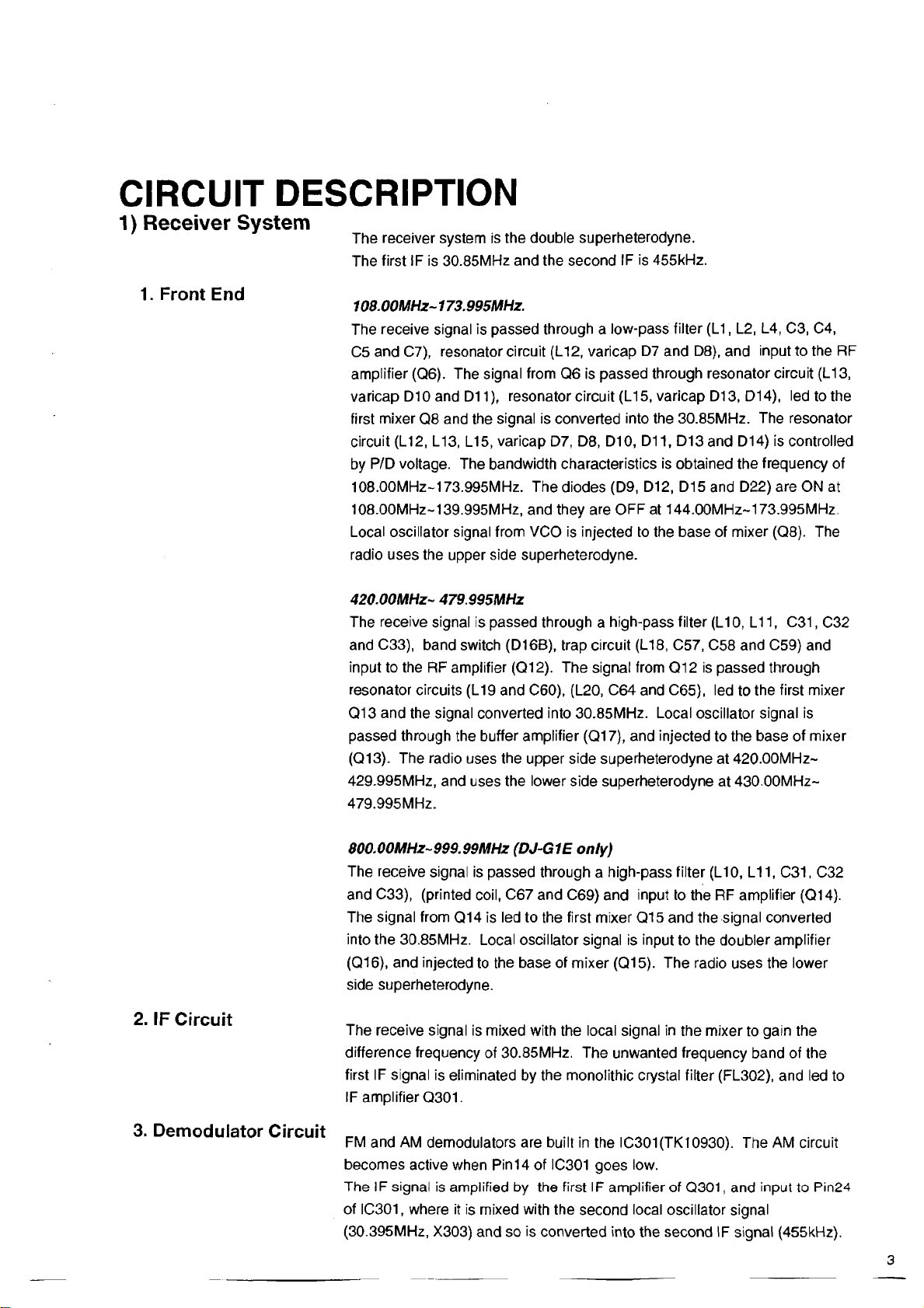
SPECIFICATIONS
1) General
Frequency Coverage:
Modulation:
Antenna Impedance:
Antenna Connector:
Power Supply Voltage:
TX Current @7.2VDC HI/MID/LOW:
©13.8VDC HI:
RX Current @AF 200mW 8ÎÎ:
Squelched:
Battery Save Mode:
Frequency Stability:
Dimensions W x H x D:
Weight:
RX: 108.000- 173.995MHz
RX:440.000 ~ 449.995MHz
TX:144.000 - 147.995MHz
RX:144.000 - 145.995MHz
RX:430.000 - 439.995MHz
TX:144.000 - 145.995MHz
F3E
A3 (receive only)
50£2
BNC
7.2-12.0V DC max.13.8VDC
approx. i 0A/0.8A/0.4A
approx. 1.6A
approx. 120mA
approx. 55mA
approx. 25mA ave.
5p.p.m.
50mm x 116mm x 37mm
360gr.
(T version)
(T version)
(T version)
(E version)
(E version)
(E version)
2) Transmitter
Output Power HI:
MID:
LOW:
Modulation:
Max. Deviation:
Spurious Emission:
Microphone Impedance:
3) Receiver
Receiving System:
IF1st/2nd:
Sensitivity (12dB SINAD):
Selectivity -6dB:
-60dB
Spurious Ratio:
Audio Output (@10% distortion):
approx. 5W (13.8VDC) 1.5W (7.2V)
approx. 1W
approx. 0.2W
Variable Reactance
+/ -5kHz
not more than -60dB
2kQ
Double Conv. Super-Heterodyne
30.85MHz/455kHz
TX Band Center max. -16dBp.
RX Subband Center (about 440MHz) max. -10dB(i
not less than 12kHz
not more than 30kHz
not more than -60dB
min. 200mW 8ii
2
Page 3
CIRCUIT DESCRIPTION
1 ) Receiver System
The receiver system is the double superheterodyne.
The first IF is 30.85MHz and the second IF is 455kHz.
1. Front End
108.00MHz~ 173.995MHz.
The receive signal is passed through a low-pass filter (L1, L2, L4, C3, C4,
C5 and C7), resonator circuit (L12, varicap D7 and D8), and input to the RF
amplifier (Q6). The signal from Q6 is passed through resonator circuit (L13,
varicap D10 and D11), resonator circuit (L15, varicap D13, D14), led to the
first mixer Q8 and the signal is converted into the 30.85MHz. The resonator
circuit (L12, L13, L15, varicap D7, D8, D10, D11, D13 and D14) is controlled
by P/D voltage. The bandwidth characteristics is obtained the frequency of
108.00MHz~173.995MHz. The diodes (D9, D12, D15 and D22) are ON at
108.00MHz~ 139.995MHz, and they are OFF at 144.00MHz~173.995MHz.
Local oscillator signal from VCO is injected to the base of mixer (Q8). The
radio uses the upper side superheterodyne.
420.00MHz~ 479.995MHz
The receive signal is passed through a high-pass filter (L10, L11, C31, C32
and C33), band switch (D16B), trap circuit (L18, C57, C58 and C59) and
input to the RF amplifier (Q12). The signal from Q12 is passed through
resonator circuits (L19 and C60), (L20, C64 and C65), led to the first mixer
Q13 and the signal converted into 30.85MHz. Local oscillator signal is
passed through the buffer amplifier (Q17), and injected to the base of mixer
(Q13). The radio uses the upper side superheterodyne at 420.00MHz~
429.995MHz, and uses the lower side superheterodyne at 430.00MHz-
479.995MHz.
2. IF Circuit
3. Demodulator Circuit
800.00MHz-999.99MHz (DJ-G1E only)
The receive signal is passed through a high-pass filter (L10, L11, C31, C32
and C33), (printed coil, C67 and C69) and input to the RF amplifier (Q14).
The signal from Q14 is led to the first mixer Q15 and the signal converted
into the 30.85MHz. Local oscillator signal is input to the doubler amplifier
(Q16), and injected to the base of mixer (Q15). The radio uses the lower
side superheterodyne.
The receive signal is mixed with the local signal in the mixer to gain the
difference frequency of 30.85MHz. The unwanted frequency band of the
first IF signal is eliminated by the monolithic crystal filter (FL302), and led to
IF amplifier Q301.
FM and AM demodulators are built in the IC301(TK 10930). The AM circuit
becomes active when Pin 14 of IC301 goes low.
The IF signal is amplified by the first IF amplifier of Q301, and input to Pin24
of IC301, where it is mixed with the second local oscillator signal
(30.395MHz, X303) and so is converted into the second IF signal (455kHz).
Page 4
The 455kHz second IF signal is output from Pin3 of IC301, and unwanted
frequency band of the second IF signal is eliminated by a ceramic filter
(FL301). The resulting signal is led to the Pin5 and 7 of IC301.
Demodulator of FM
The second IF signal of Pin7 of IC301 is led to the internal limiter amplifier,
quadrature detection circuit. The audio signal is output from Pin 12 of IC301.
Demodulator of AM
The second IF signal of Pin5 of IC301 is led to the internal AM amplifier, AM
detection circuit. The audio signal is output from Pin 13 of IC301.
The AGC circuit is used to obtain a stable audio output level even if the input
level is changed. The forward AGC signal is output from Pin 18 of IC301,
and input to the AGC amplifier (Q326). The gain of the first IF amplifier is
controlled by the AGC signal.
4. Audio Circuit
FM Mode
The audio signal from Pin12 of IC301, which is pre-emphasized on transmit
ting, is led to the emphasis circuit (R334 and C338) and compensated for
the audio frequency characteristics. The audio signal is amplified by AF
amplifier (Q306), led to the audio H.P.F. (Q310, C346, C347 and R346).
The audio signal is input to the volume (VR311), and input to the power
amplifier Pin3 of IC305, and output from Pin6 to drive the speaker.
AM Mode
When you select the AM mode, switching transistors Q324, Q308 and Q309
become ON, and then Pin14 of IC301 goes to Low (AM detection circuit is
active), Q307 is active and Q306 is not active. The audio signal from Pin13
of IC301 is amplified by AF preamplifier (Q307), led to the audio H.P.F.
(Q310, C346, C347 and R346), as well as in the FM mode, then input to the
volume (VR311) and the power amplifier to drive the speaker.
Note
The IC301 (TK10930) of the FM detection circuit is active even in the AM
mode, FM detector circuit is active. Q306 connects the base of the FM
audio preamplifier Q309 to the ground so that the FM audio signal by the FM
detection is cut.
5. Squelch Circuit
The noise in the audio signal from Pin 12 of detection IC, IC301 is passed
through the squelch control variable resistor (VR311) and input to the noise
filter amplifier consisting of C323, C322, C325, R317 and R316, internal
noise amplifier IC301. The desired noise of the audio signal is output from
Pin20 of IC301 and so amplified by noise amplifier (Q305). The amplified
noise signal is rectified by D302 and then input to Pin21 of IC301. When the
voltage of Pin21 is above 0.7V, Pin22 of IC301 goes to "low" (squelch circuit
is active). When the voltage of Pin21 is below 0.7V, Pin22 of IC301 goes to
Page 5
"High" (squelch circuit does not work). This signal "SD" is led to the CPU
Pin of IC401, and then processed by CPU. When the squelch circuit is
active, Q311 and Q304 are off. When the squelch circuit does not work,
Q311 and Q304 are on. In this way the audio output signal is controlled.
When the squelch circuit does not work, Q323 goes on, the squelch indicator
LED (D303B) light turns on. When the squelch circuit is active, Q323 goes
off, the squelch indicator LED (D303B) light turns off.
6. Audio Power
Amplifier Circuit
7. Signal Meter
Circuit
2) Transmitter System
1. Microphone Amplifier
Modulator Circuit
When the power supply voltage of radio becomes above 6.3V in the voltage
stabilizer circuit (Q302, Q303, D301 and D304). The power supply voltage of
audio power amplifier IC (IC305) is controlled below 6.3V.
The voltage of audio power amplifier IC (IC305) is controlled by the Q304.
The Q304 is ON when the squelch is OFF, BEEP sound is outputting, and
DTMF monitor (TX) is ON, then IC305 works.
The IC301 has S meter function. When the signal strength is low, voltage of
Pin 16 becomes lower, and when the signal strength is high, voltage of Pin
16 becomes higher. The S meter voltage of Pin 16 is led to the variable
resistor (VR310) and input to the Pin of IC401 (CPU). It is converted by A/D
converter built-in CPU, and S is appeared in the LCD.
After the voice is converted into the electric signal through the internal or
external microphone, the signal is led to the microphone amplifier IC304.
IC304 consists of two operational amplifiers. One operational amplifier (Pin5,
6 and 7) uses pre-emphasis circuit and IDC circuit, and the other operational
amplifier (Pin1, 2 and 3) uses splatter filter. The output from the microphone
amplifier is passed through variable resistors VR305 for maximum deviation
adjustment to cathode of varicap (D206) diode of the VCO, controlling the
VCO frequency and so producing a frequency-modulation.
2. Power Amplifier
Circuit
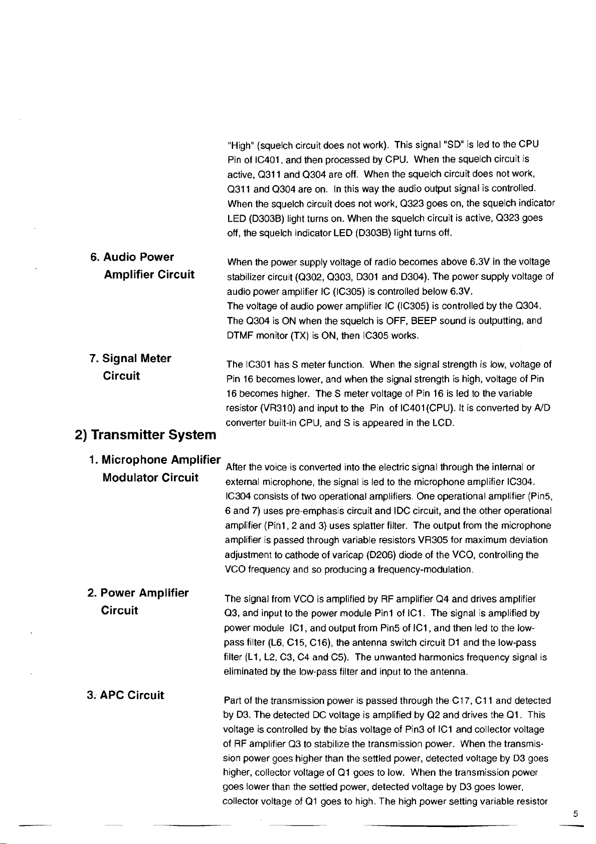
3. APC Circuit
The signal from VCO is amplified by RF amplifier Q4 and drives amplifier
Q3, and input to the power module Pin 1 of IC1. The signal is amplified by
power module IC1, and output from Pin5 of IC1, and then led to the low-
pass filter (L6, C15, C16), the antenna switch circuit D1 and the low-pass
filter (L1, L2, C3, C4 and C5). The unwanted harmonics frequency signal is
eliminated by the low-pass filter and input to the antenna.
Part of the transmission power is passed through the C17, C11 and detected
by D3. The detected DC voltage is amplified by Q2 and drives the Q1. This
voltage is controlled by the bias voltage of Pin3 of IC1 and collector voltage
of RF amplifier Q3 to stabilize the transmission power. When the transmis
sion power goes higher than the settled power, detected voltage by D3 goes
higher, collector voltage of Q1 goes to low. When the transmission power
goes lower than the settled power, detected voltage by D3 goes lower,
collector voltage of Q1 goes to high. The high power setting variable resistor
Page 6
VR308 and the middle power setting variable resistor VR307 located in the
IF unit. The radio has no low power setting variable resistor.
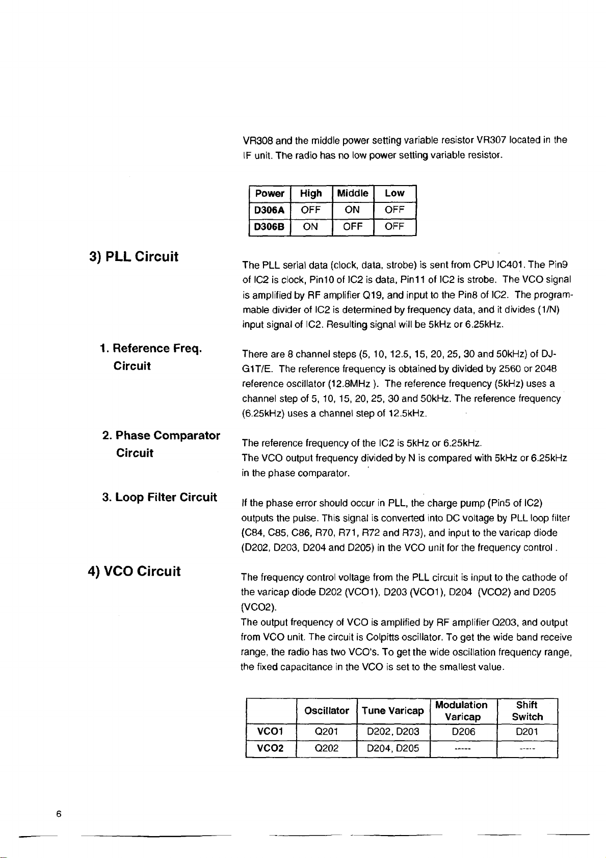
3) PLL Circuit
1. Reference Freq.
Circuit
2. Phase Comparator
Circuit
Power
D306A
D306B
The PLL serial data (clock, data, strobe) is sent from CPU IC401. The Pin9
of IC2 is clock, Pin10 of IC2 is data, Pin 11 of IC2 is strobe. The VCO signal
is amplified by RF amplifier Q19, and input to the Pin8 of IC2. The program
mable divider of IC2 is determined by frequency data, and it divides (1/N)
input signal of IC2. Resulting signal will be 5kHz or 6.25kHz.
There are 8 channel steps (5, 10, 12.5, 15, 20, 25, 30 and 50kHz) of DJ-
G1T/E. The reference frequency is obtained by divided by 2560 or 2048
reference oscillator (12.8MHz). The reference frequency (5kHz) uses a
channel step of 5, 10, 15, 20, 25, 30 and 50kHz. The reference frequency
(6.25kHz) uses a channel step of 12.5kHz.
The reference frequency of the IC2 is 5kHz or 6.25kHz.
The VCO output frequency divided by N is compared with 5kHz or 6.25kHz
in the phase comparator.
High Middle
OFF ON
ON OFF
Low
OFF
OFF
3. Loop Filter Circuit
4) VCO Circuit
If the phase error should occur in PLL, the charge pump (Pin5 of IC2)
outputs the pulse. This signal is converted into DC voltage by PLL loop filter
(C84, C85, C86, R70, R71, R72 and R73), and input to the varicap diode
(D202, D203, D204 and D205) in the VCO unit for the frequency control.
The frequency control voltage from the PLL circuit is input to the cathode of
the varicap diode D202 (VC01), D203 (VC01), D204 (VC02) and D205
(VC02).
The output frequency of VCO is amplified by RF amplifier Q203, and output
from VCO unit. The circuit is Colpitts oscillator. To get the wide band receive
range, the radio has two VCO's. To get the wide oscillation frequency range,
the fixed capacitance in the VCO is set to the smallest value.
Oscillator
VC01 Q201
VC02
Q202
Tune Varicap
D202, D203
D204, D205
Modulation
Varicap
D206 D201
Shift
Switch
Page 7
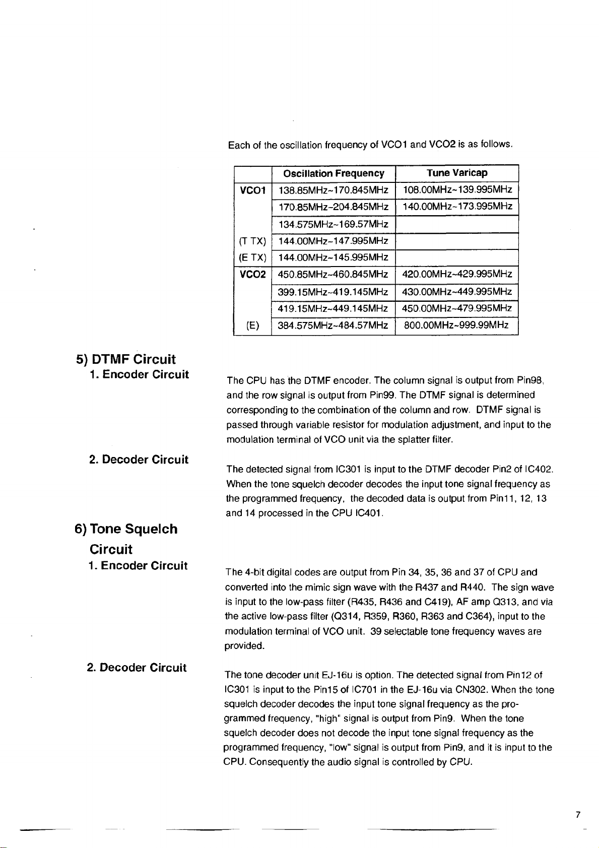
Each of the oscillation frequency of VC01 and VC02 is as follows.
5) DTMF Circuit
1. Encoder Circuit
2. Decoder Circuit
6) Tone Squelch
Oscillation Frequency
VC01
(TTX)
(E TX)
VC02
(E)
The CPU has the DTMF encoder. The column signal is output from Pin98,
and the row signal is output from Pin99. The DTMF signal is determined
corresponding to the combination of the column and row. DTMF signal is
passed through variable resistor for modulation adjustment, and input to the
modulation terminal of VCO unit via the splatter filter.
The detected signal from IC301 is input to the DTMF decoder Pin2 of IC402.
When the tone squelch decoder decodes the input tone signal frequency as
the programmed frequency, the decoded data is output from Pinll, 12, 13
and 14 processed in the CPU IC401.
138.85MHz~170.845MHz
170.85MHz~204.845MHz
134.575MHz~169.57MHz
144.00MHZ-147.995MHz
144.00MHz-145.995MHz
450.85MHz~460.845MHz
399.15MHz~419.145MHz
419.15MHZ-449.145MHz
384.575MHz~484.57MHz
Tune Varicap
108.00MHz~ 139.995MHz
140.00MHz~173.995MHz
420.00MHz~429.995MHz
430.00MHz~449.995MHz
450.00MHz~479.995MHz
800.00MHz~999.99M Hz
Circuit
1. Encoder Circuit
2. Decoder Circuit
The 4-bit digital codes are output from Pin 34, 35, 36 and 37 of CPU and
converted into the mimic sign wave with the R437 and R440. The sign wave
is input to the low-pass filter (R435, R436 and C419), AF amp Q313, and via
the active low-pass filter (Q314, R359, R360, R363 and C364), input to the
modulation terminal of VCO unit. 39 selectable tone frequency waves are
provided.
The tone decoder unit EJ-16u is option. The detected signal from Pin 12 of
IC301 is input to the Pin15of IC701 in the EJ-16uvia CN302. When the tone
squelch decoder decodes the input tone signal frequency as the pro
grammed frequency, "high" signal is output from Pin9. When the tone
squelch decoder does not decode the input tone signal frequency as the
programmed frequency, "low" signal is output from Pin9, and it is input to the
CPU. Consequently the audio signal is controlled by CPU.
Page 8
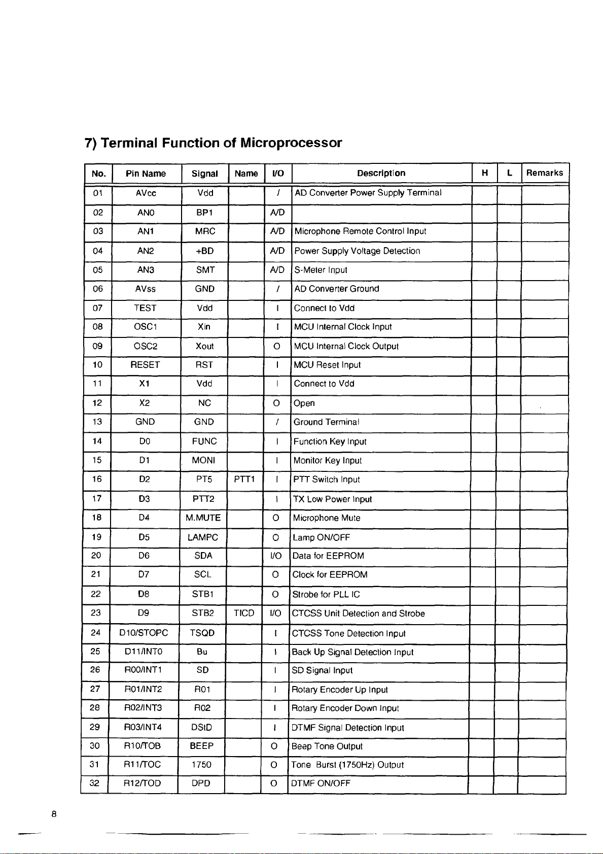
7) Terminal Function of Microprocessor
No. Pin Name
01 AVcc Vdd
02
03
04
05
06
07
08
09
10
11 X1
12
13 GND
14
15
AN0
AN1 MRC
AN2
AN3
AVss GND /
TEST
OSC1
OSC2
RESET
X2 NC O
DO FUNC I
D1 MONI I
Signal
BP1 A/D
+BD
SMT
Vdd I Connect to Vdd
Xin
Xout
RST
Vdd
GND /
Name
I/O
AD Converter Power Supply Terminal
/
A/D
Microphone Remote Control Input
A/D Power Supply Voltage Detection
S-Meter Input
A/D
AD Converter Ground
Description H L Remarks
I MCU Internal Clock Input
O MCI) Internal Clock Output
I
MCU Reset Input
I
Connect to Vdd
Open
Ground Terminal
Function Key Input
Monitor Key Input
16
17
18 D4
19
20
21
22
23 D9 STB2
24
25 D11/INT0
26 R 00/INT 1
27
28
29
30 RIO/TOB BEEP
31
D2
D3
D5
D6
D7 SCL
D8
DIO/STOPC TSQD
R01/INT2
R02/INT3 R02 I
R03/INT4
R11/TOC 1750
PT5
PTT2
M.MUTE
LAM PC
SDA
STB1
Bu I
SD I
R01 I
DSlD I
PTT1 I
TICD
PTT Switch Input
I TX Low Power Input
0 Microphone Mute
Lamp ON/OFF
0
I/O Data for EEPROM
0 Clock for EEPROM
Strobe for PLL IC
0
I/O CTCSS Unit Detection and Strobe
I CTCSS Tone Detection Input
Back Up Signal Detection Input
SD Signal Input
Rotary Encoder Up Input
Rotary Encoder Down Input
DTMF Signal Detection Input
Beep Tone Output
0
Tone Burst (1750Hz) Output
0
32
R12/TOD DPD o
DTMF ON/OFF
Page 9
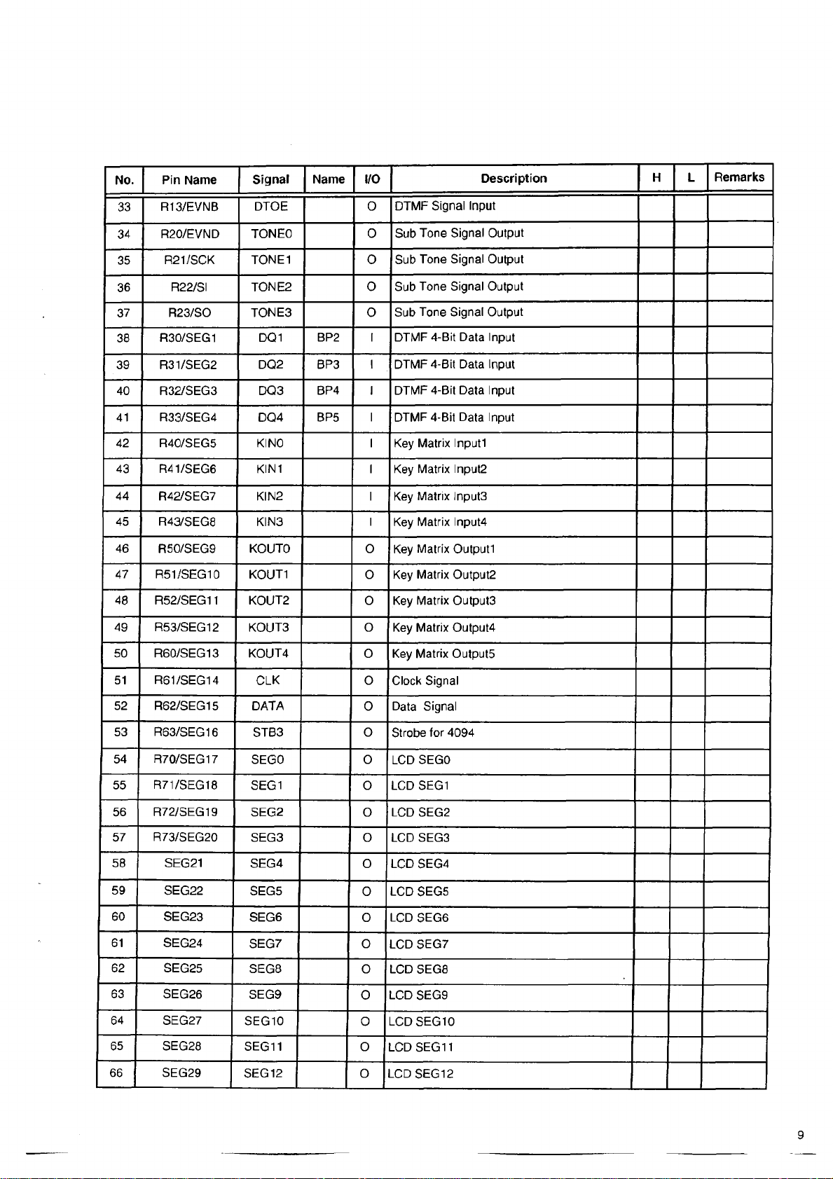
No.
Pin Name
Signal Name I/O
Description
H L
Remarks
33 R13/EVNB
34 R20/EVND
35
36
37
38 R30/SEG1
39 R31/SEG2
40 R32/SEG3 DQ3
41
42
43 R41/SEG6
44 R42/SEG7 KIN2
45
46
47
48
R21/SCK
R22/SI
R23/SO TONE3 0
R33/SEG4 DQ4
R40/SEG5
R43/SEG8
R50/SEG9 KOUTO o Key Matrix Outputl
R51/SEG10
R52/SEG11 KOUT2
DTOE 0
TONEO 0
TONE1
TONE2 0
DQ1
DQ2
KIN0 I Key Matrix Inputl
KIN1
KIN3 I
KOÜT1
DTMF Signal Input
Sub Tone Signal Output
Sub Tone Signal Output
0
Sub Tone Signal Output
Sub Tone Signal Output
BP2 I DTMF 4-Bit Data Input
BP3
BP4
BP5
I DTMF 4-Bit Data Input
I DTMF 4-Bit Data Input
I
DTMF 4-Bit Data Input
I Key Matrix Input2
Key Matrix Input3
I
Key Matrix Input4
o Key Matrix Output2
o Key Matrix Output3
49 R53/SEG12 KOUT3 o Key Matrix Output4
50 R60/SEG13 KOÜT4
51 R61/SEG14
52
R62/SEG15
53
R63/SEG16 STB3 o Strobe for 4094
54 R70/SEG17
55 R71/SEG18
56 R72/SEG19
57
R73/SEG20
58 SEG21 SEG4
59
60
61 SEG24
62
63
64
SEG22
SEG23 SEG6
SEG25
SEG26
SEG27
CLK
DATA
SEGO o
SEG1 o LCD SEG1
SEG2
SEG3 o
SEG5
SEG7
SEG8
SEG9
SEG10
o Key Matrix Output5
o
Clock Signal
0 Data Signal
LCD SEGO
o LCD SEG2
LCD SEG3
o LCD SEG4
0 LCD SEG5
o LCD SEG6
o
LCD SEG7
o LCD SEG8
LCD SEG9
0
0 LCD SEG10
65
66 SEG29
SEG28
SEG11 o
SEG12
o
LCD SEG11
LCD SEG12
Page 10
No. Pin Name Signal
Name I/O
Description H
L
Remarks
67
68 SEG31
69
70
71
72 SEG35 SEG18
73 SEG36 SEG19
74
75 SEG38 SEG21 0
76 SEG39 SEG22 0
77
78
79
80 SEG43
81
82
SEG30
SEG32 SEG15
SEG33
SEG34 SEG17 0
SEG37
SEG40
SEG41 SEG24
SEG42
SEG44
SEG45 SEG28 0 LCD SEG28
SEG13 O
SEG14
SEG16 0
SEG20 0
SEG23
SEG25 0 LCD SEG25
SEG26
SEG27 0 LCD SEG27
LCD SEG13
LCD SEG14
O
LCD SEG15
0
LCD SEG16
LCD SEG17
0 LCD SEG18
0 LCD SEG19
LCD SEG20
LCD SEG21
LCD SEG22
LCD SEG23
o
LCD SEG24
0
0 LCD SEG26
83
84 SEG47
85
86
87
88 SEG51 SEG34
89 SEG52 SEG35
90 COM1
91 COM2 COM1
92
93
94
95
96 V3
97
98 TON EC
SEG46 SEG29
SEG30 0 LCD SEG30
SEG48 SEG31
SEG49
SEG50
COM3 COM2 0
COM4
V1
V2 VL2
Vcc Vdd
SEG32 0 LCD SEG32
SEG33 0
COMO 0 LCD COMO
NC
VL1
VL3
DTONC
LCD SEG29
o
0 LCD SEG31
LCD SEG33
LCD SEG34
0
LCD SEG35
0
o LCD COM1
LCD COM2
0
/ LCD Power Supply
LCD Power Supply
/
/
LCD Power Supply
/
Power Supply
0 Column Output for DTMF Signal
10
99 TONER
100
VTref Vdd I
DTONR
0
Row Output for DTMF Signal
Reference Power Supply for DTMF Output
Page 11
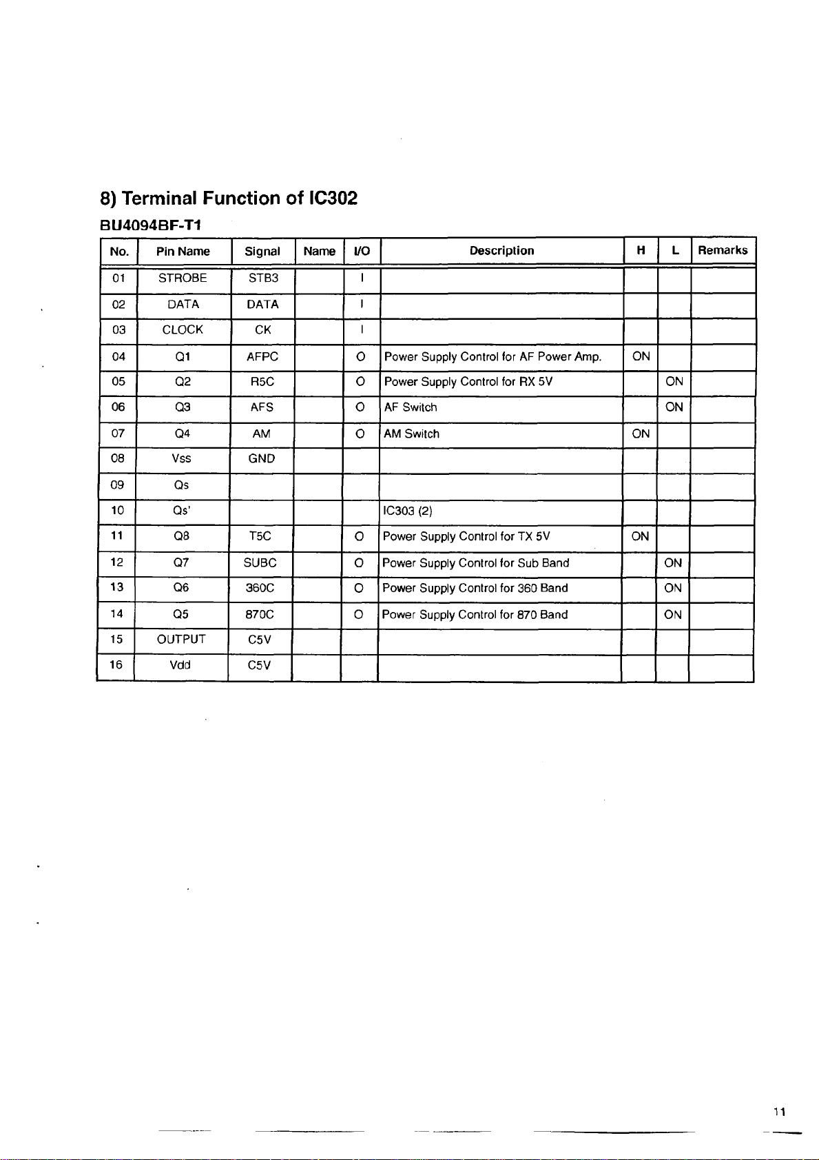
8) Te r min a l Function of IC 3 02
BU4094BF-T1
No. Pin Name Signal Name
01
02
03
04
05 Q2
06 Q3
07
08 Vss
09 Qs
10
11
12
13
14
15
STROBE
DATA
CLOCK
Q1
Q4
Os’ IC303 (2)
Q3
Q7
Q6
Q5
OUTPUT
STB3
DATA
CK
AFPC
R5C O Power Supply Control for RX 5V
AFS
AM
GND
T5C
SUBC 0
360C
870C 0 Power Supply Control for 870 Band ON
C5V
I/O
I
I
I
Power Supply Control for AF Power Amp.
O
AF Switch
0
AM Switch
0
0 Power Supply Control for TX 5V ON
Power Supply Control for Sub Band ON
Power Supply Control for 360 Band ON
0
Description
ON
ON
H L
ON
ON
Remarks
16 Vdd
C5V
11
Page 12
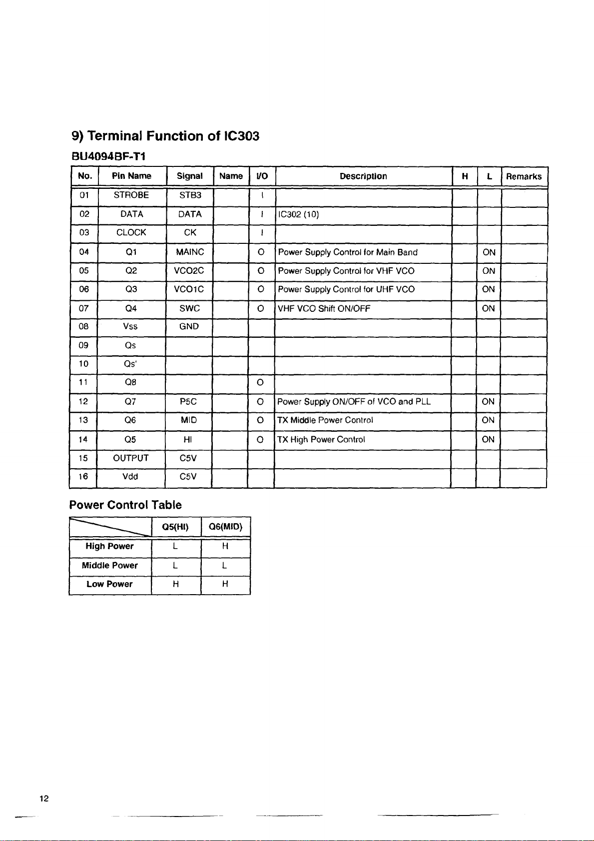
9) Te r mina l Fun c t io n of IC3 03
BU4094BF-T1
No. Pin Name
01 STROBE
02
03 CLOCK
04
05 Q2 VC02C
06
07 Q4
08
09 Qs
10
11
12
13
14
15
DATA DATA I
Q1
Q3
Vss
Os'
Q8
Q7 P5C
Q6
Q5 HI
OUTPUT
Signal
STB3
CK I
MAINC O Power Supply Control for Main Band
VC01C O Power Supply Control for UHF VCO ON
SWC
GND
MID
C5V
Name
I/O Description H L
I
IC302 (10)
ON
O Power Supply Control (or VHF VCO ON
O VHF VCO Shift ON/OFF
O
Power Supply ON/OFF of VCO and PLL
O
O TX Middle Power Control
TX High Power Control ON
0
ON
ON
ON
Remarks
16
Vdd
Power Control Table
C5V
Page 13
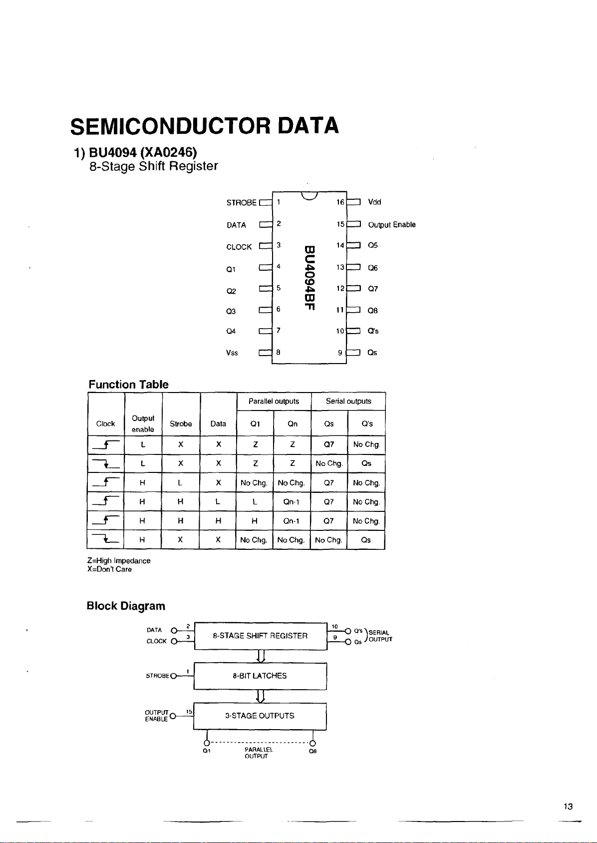
SE MI CO ND UC TO R DA T A
1) B U40 9 4 (XA0246)
8-Stage Shift Register
w
STROBE HZ
1
16
=l
Vdd
Function Table
Clock
s ~
Output
enable
L X
L X
H
H H
DATA \zz
CLOCK
Q1
Q2
Q3
04
Vss
Strobe
L X No Chg. No Chg. 0 7 No Chg.
Data
X
X
L
2
3
cz
cz
ÜZ
r z
cz
n z
Parallel outputs Serial outputs
Q 1
Z Z
Z
L
00
c
4
O
CO
5
-U
03
n
6
7
8
Qn Qs Q's
Z
Qn-l
15
z □
14
Z J
13
ZD
12
ZZ1 Q7
11
zz
10 Q's
9
Q7 No Chg.
No Chg.
Q7 No Chg.
Output Enable
Q5
Q6
Q8
Qs
Qs
H
!k -
Z=High Impedance
X=Don't Care
H X X
Block Diagram
H H
Q1 PARALLEL Q8
H
No Chg. No Chg. No Chg.
OUTPUT
Qn-1
Q7 No Chg.
Qs
Page 14
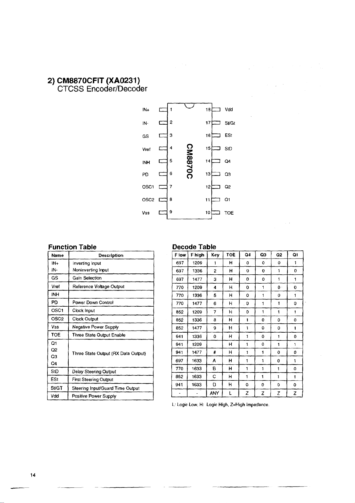
2) CM8870CFIT (XA0231)
CTCSS Encoder/Decoder
Function Table
Name Description
IN+ Inverting Input
IN-
GS Gain Selection
Vref Reference Voltage Output
INH
PD Power Down Control
OSC1
OSC 2
Vss
TOE
Q1
Q2
Q3
Q4
StD
ESt
St/GT Steering Input/Guard Time Output
Vdd Positive Power Supply
Noninverting Input
Clock Input
Clock Output
Negative Power Supply
Three State Output Enable
Three State Output (RX Data Output)
Delay Steering Output
First Steering Output
IN+
CJ
cz
IN-
cz
GS
cz
Vref
cz=
INH
cz:
PD
OSC1
zz
OSC2
a
Vss cz
1
2
3 16
o
4
2
00
5
CO
o
6
O
7
8
9
18
17
15
14
13
12
11
10
Decode Ta
F high Key TOE
F low
697 1209
697 1336
697 1477
770 1209 4 H 0
770
1336 5 H 0 1 0 1
770 1477
1209 7 H 0
852
1336 8 H 1 0
852
1477
852
641 1336
941 1209
941 1477
697
1633
770 1633 B H 1 1
852 1633 C H 1 1 1
941
1633
-
L: Logic Low, H: Logic High, Z=High Impedance.
Vdd
ZD
St/Gt
=3
ESt
ZD
IZ)
StD
ZZ 0 4
ZZl 03
Q2
ZZI
Q1
ZD
bn
TOE
ble
Q4
Q3
H 0 0
1
0
H
2
H
3
H
6
9
0 H
# H 1 1 0 0
A H
D
ANY
. 0
H 1 0
H
H
L z
0
0
0
1
1
1
1
0
0
1
1
1
0 0 0
z
02 Q1
0 1
1 0
1
0 0
1
1
0
0 1
1
1
0 1
1
z
1
0
1
0
0
1
0
1
0
z
Page 15
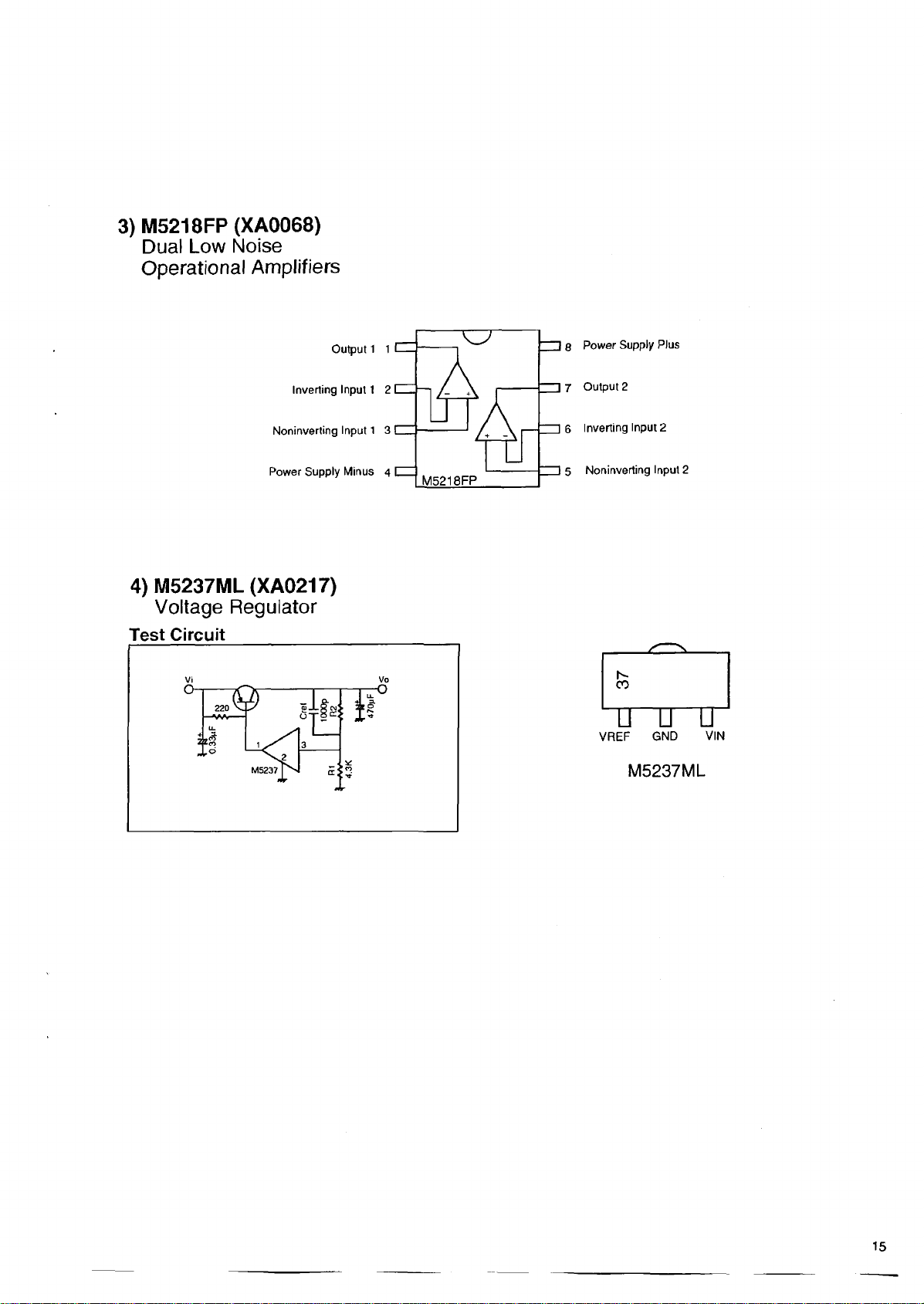
3 ) M 5 218FP (X A00 68)
Dual Low Noise
Operational Amplifiers
Inverting Input 1 2 [
Noninverting Input 1 3 [
Power Supply Minus 4 I
4 ) M5237ML (X A02 1 7 )
Voltage Regulator
Test Circuit
Vi Vo
Output 1 1 I
I e Power Supply Plus
| 7 Output 2
| 6 Inverting Input 2
I 5 Noninverting Input 2
M5237ML
Page 16
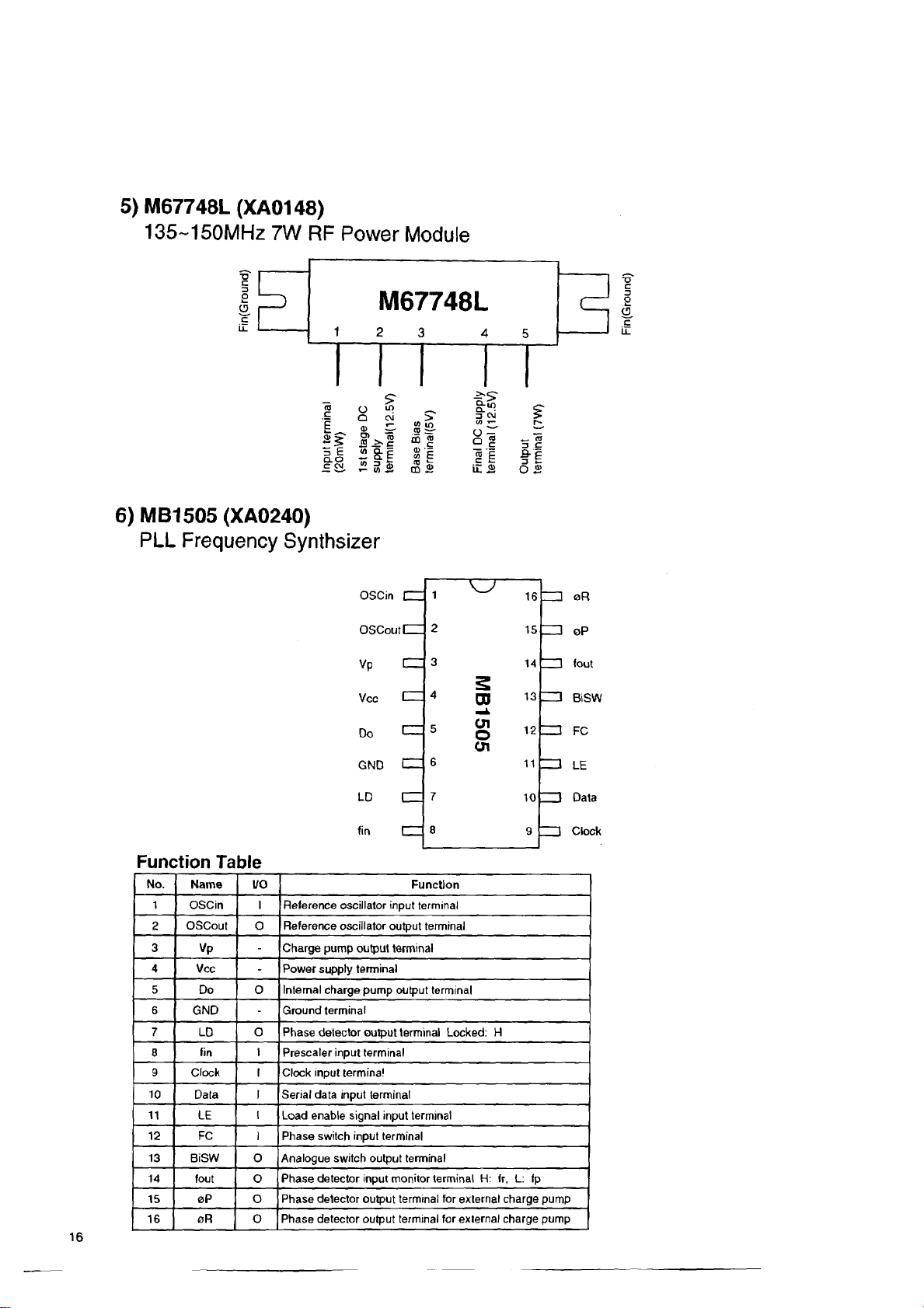
5) M67748L (XA0148)
135~150MHz 7W RF Power Module
6) MB1505 (XA0240)
PLL Frequency Synthsizer
OSCin
CZZ
Fin(Ground)
W
1
16
zn
aR
16
OSC o u tIZ Z
cz
Vp
czz
Vcc
czz
Do
CZ Z
GND
LD
c z
fin
czz
2
3
2
4
GO
_ l
cn
5
o
cn
6
7
8
15
14
13
12
11
10
9
Function Table
No.
Name I/O
1
OSCin I
OSCout o Reference oscillator output terminal
2
3 Vp
4
Vcc
5
6
7
8 fin
9
10 Data I Serial data input terminal
11 LE
12 FC I Phase switch input terminal
13 BiSW 0 Analogue switch output terminal
14
15 0 P o Phase detector output terminal for external charge pump
16 oR o
Do 0 Internal charge pump output terminal
GND
LD
Clock I Clock input terminal
tout o
Reference oscillator input terminal
-
Charge pump output terminal
Power supply terminal
-
Ground terminal
-
o
Phase detector output terminal Locked: H
I
Prescaler input terminal
I
Load enable signal input terminal
Phase detector input monitor terminal H: (r, L: fp
Phase detector output terminal for external charge pump
Function
ZD
zn
z□
ZD FC
ZZ3
= □
oP
(out
BiSW
LE
Data
Clock
Page 17
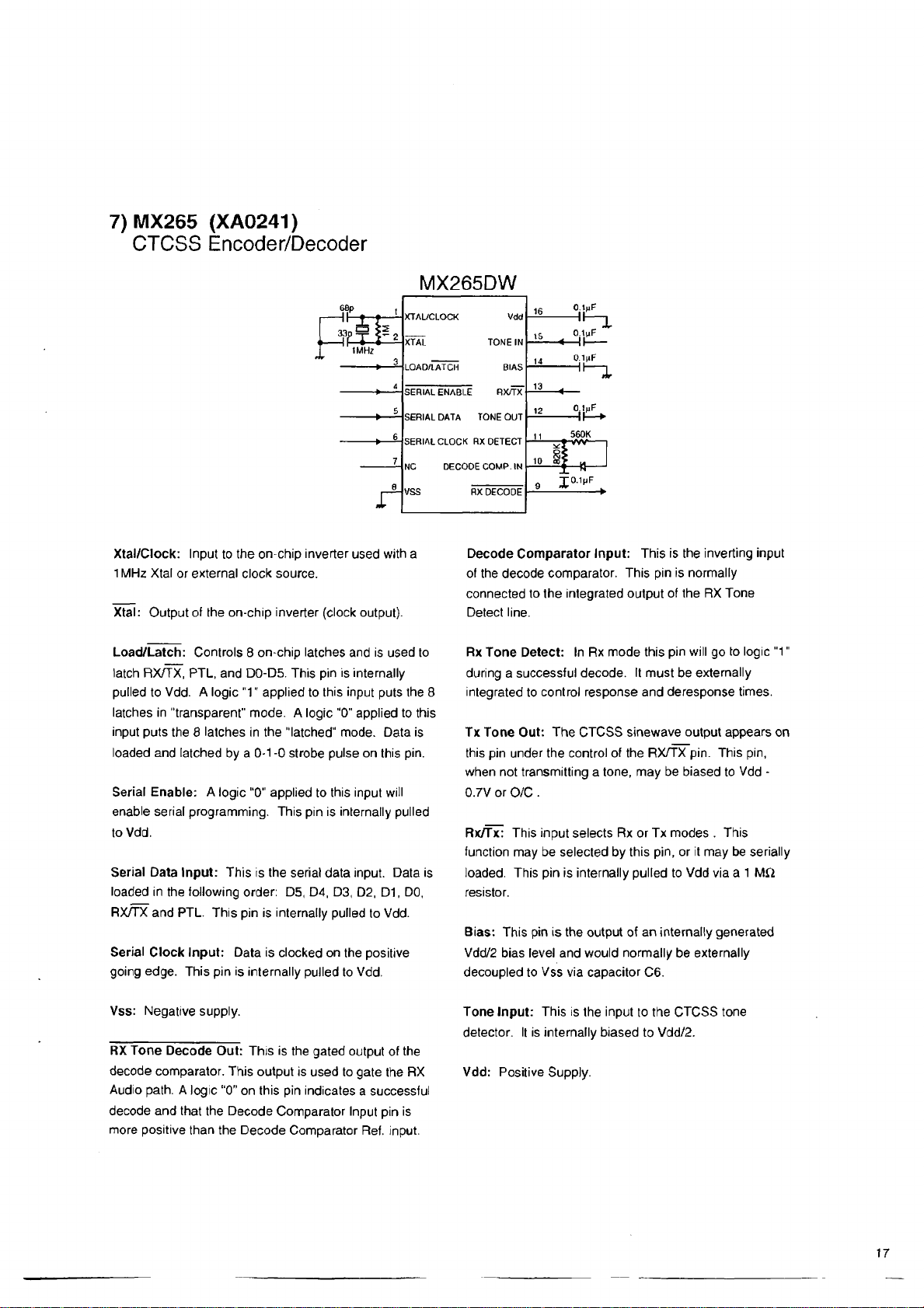
7) MX265 (XA0241 )
CTCSS Encoder/Decoder
6Bp
a <5
'p L iZ l
MX265DW
XTAL/CLOCK Vdd
XTAL TONE IN
LOAD/LATCH
SERIAL ENABLE RttTX
SERIAL DATA TONE OUT
SERIAL CLOCK RX DETECT
NC DECODE COMP. IN
VSS
J T
BIAS
RX DECODE
0.1MF
HI—
O.IijF
-«—II
----
O.lnF
-----II---
0.1MF
560K
-vw—
- 4 - » -
X°.,mf
Xtal/Clock: Input to the on-chip inverter used with a
1 MHz Xtal or external clock source.
Xtal: Output of the on-chip inverter (clock output).
Load/Latch: Controls 8 on-chip latches and is used to
latch RX/TX, PTL, and D0-D5. This pin is internally
pulled to Vdd. A logic "1" applied to this input puts the 8
latches in "transparent" mode. A logic “0" applied to this
input puts the 8 latches in the "latched" mode. Data is
loaded and latched by a 0-1 -0 strobe pulse on this pin.
Serial Enable: A logic "0" applied to this input will
enable serial programming. This pin is internally pulled
to Vdd.
Serial Data Input: This is the serial data input. Data is
loaded in the following order: D5, D4, D3, D2, D1, DO,
RX/TX and PTL. This pin is internally pulled to Vdd.
Serial Clock Input: Data is clocked on the positive
going edge. This pin is internally pulled to Vdd.
Decode Comparator Input: This is the inverting input
of the decode comparator. This pin is normally
connected to the integrated output of the RX Tone
Detect line.
Rx Tone Detect: In Rx mode this pin will go to logic "1"
during a successful decode. It must be externally
integrated to control response and deresponse times.
Tx Tone Out: The CTCSS sinewave output appears on
this pin under the control of the RX/TX pin. This pin,
when not transmitting a tone, may be biased to Vdd -
0.7V or O/C.
Rx/Tx: This input selects Rx or Tx modes . This
function may be selected by this pin, or It may be serially
loaded. This pin is internally pulled to Vdd via a 1 MC2
resistor.
Bias: This pin is the output of an internally generated
Vdd/2 bias level and would normally be externally
decoupled to Vss via capacitor C6.
Vss: Negative supply.
RX Tone Decode Out: This is the gated output of the
decode comparator. This output is used to gate the RX
Audio path. A logic "0" on this pin indicates a successful
decode and that the Decode Comparator Input pin is
more positive than the Decode Comparator Ref. input.
Tone Input: This is the input to the CTCSS tone
detector. It is internally biased to Vdd/2.
Vdd: Positive Supply.
Page 18
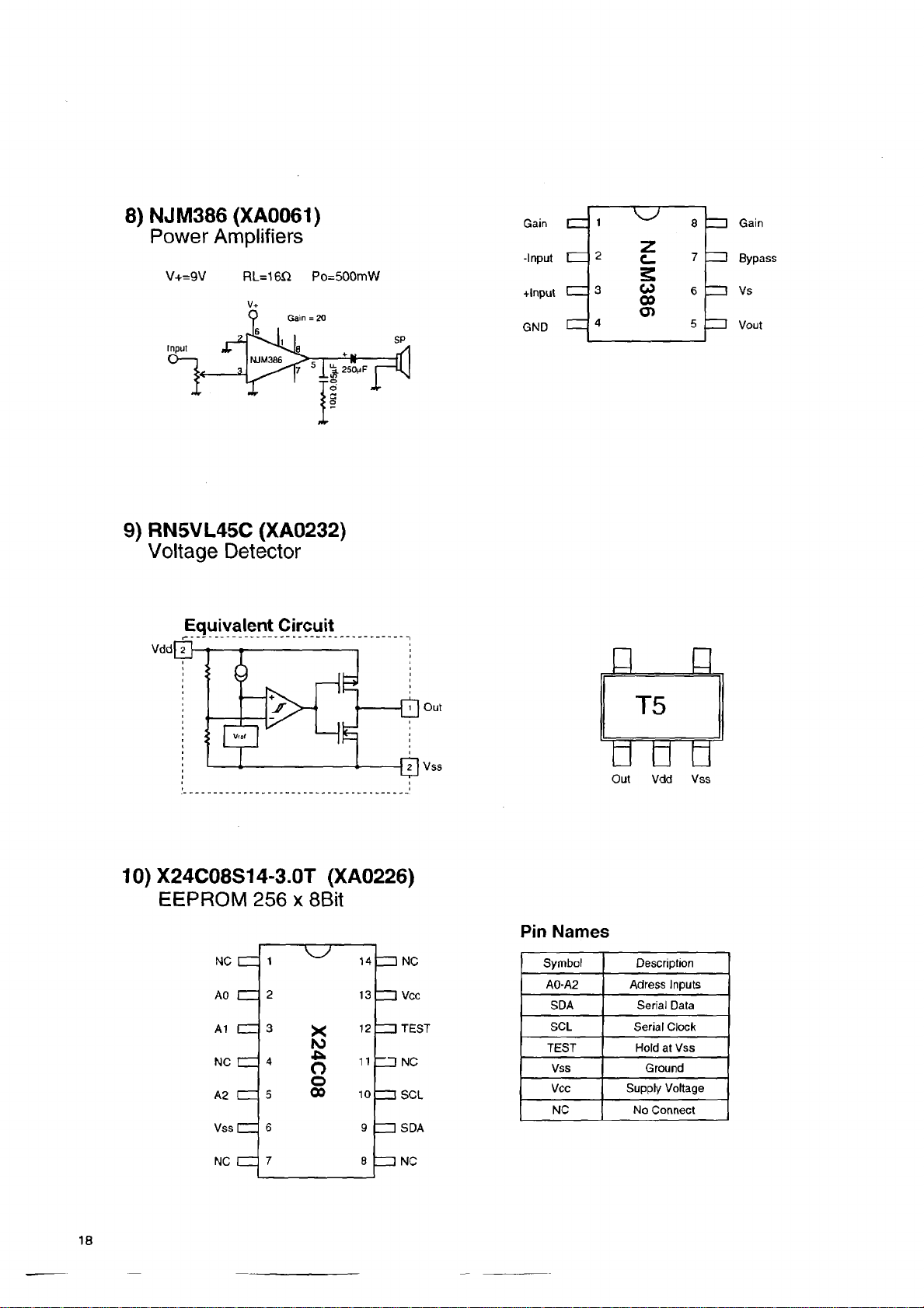
8) NJM386 (XA0061)
Power Amplifiers
V+=9V RL=16fi Po=500mW
9) RN5VL45C (XA0232)
Voltage Detector
Equivalent Circuit
Gain
-Input
+tnput
GND
d
n z
n z
c =
i
z
2
c_
5
W
3
0 0
CT>
4
8
7
6
5
Gain
Bypass
Vs
Vout
10) X24C08S14-3.0T (XA0226)
EEPROM 256 x 8Bit
w
NC IZ Z
AO d
A1 [ZZ
NC C Z
A2 C Z
Vss IZ Z
NC C Z
1
2
3
X
ro
« h
4
o
o
0 0
5
6 9
7 8
14
Z Z NC
13
ZZ1 Vcc
12
IZ I TEST
11
Z Z I NC
10
Z Z SCL
IZ I SDA
Z ZI NC
Out Vdd Vss
Pin Names
Symbol Description
A0-A2
SDA Serial Data
SCL Serial Clock
TEST
Vss Ground
Vcc
NC No Connect
Adress Inputs
Supply Voltage
Hold at Vss
Page 19

11) TK10930VTL (XA0223)
Characterristic Symbol Min Typical
Supply Current 1 Icc1
Supply Current 2
Mixer Conversion Gain
Mixer Input Impedance
FM
Limiting Sensitivity
Output Voltage
Distortion
Output Impedance
Filter Gain
Scan Control Hi Voltage SH
Scan Control Low Voltage
Squelch Hysteresis
S meter Output Voltage
S meter Output Voltage
S meter Output Voltage
S meter Output Voltage
S meter Output Voltage S4
S meter Output Voltage
AM
Sensitivity
Output Voltage Vo2
Distortion-1
Distortion-2
S/N
AM OFF Vo
Icc2
Mg 20
Mz
Limit 2,0 8.0
Vo1 85
THD1 1 0 2.0 % 10mVin +/-3kHz DEV
Zo 800 a 10mVin
Gf 30 38 dB Fin=30kHz, Vo=100mV
SL 0.3 V
Hys
SO 0.05
S1 0.05
S2 0.7 1 2
S3 1.2 1.8 2.5 V Vin=1mV, RS=68k il
S5
US 20
THD2
THD3
Vo1 40 48
Max Typical
6.8
3.9 5.3 mA No signal, AM OFF
3.6
150 230
2.3 V Squelch input=2.5V
30 mV
0.5
1.6
1.8 2.4 2.9
60
-0.3
2.3
15
120 160 mVrms 1kHz, 30%, Vin=1mV
1.0
2.0 4.0 % 1kHz, 30%, Vin=1mV
8.9 mA No signal, AM ON
dB
DC Test
Kn
-3.0dB
pv
mVrms
0.5
0.9
1.7
2.9
2.0 %
dB
0.3 % OFF
10mVin +/-3kHz DEV
Squelch input=0V
V Vin=0mV, RS=68kil
V Vin=0.01mV, RS=6 8ktl
V Vin=0.1mV, RS=68k a
Vin=10mV, R S =60kii
V
V Vin=100mV, RS=68k n
^v
When output is 20mVrms.
1kHz, 30%, Vin=1mV
1kHz, 30%, Vin=1mV
Condition
Page 20

12) Tra n s i s to r , D iode a n d LED Outline Dr a win gs
Top View
20
Page 21
(SEG20)
48
(COM2)
(COM1) 46
(SEG21)
(S EG 19) 44
(SEG18) 43
(S EG 17)
(S EG 16)
(SEG15)
(SEG14)
(S EG 13) 38
(S EG 12)
(SEG11) 36
(SEG10)
(SEG9)
(SEGS) 33
(SEG7)
40
47
45
42
41
39
37
35
34
32
(SEG6) 31
(SEG5)
(SEG4) 29
(SEG3)
(SEG2)
(SEG1)
(SEGO)
30
28
27
26
25
Page 22

(f) _L
m co
1
SEG29)
SEG27)
2
3
SEG25)
4
SEG23)
5
SEG22)
SEG24)
6
SEG26)
7
8
COMO)
NC)
9
m
I I
10
COM1)
11
NC)
12
COMO)
SEG28)
13
NC)
14
15
NC)
o
s
m
z
H
I) LCD Co nn
(E L 0 0 23)
<D
O
5‘
3
16
NC)
17
NC)
NC)
m
18
19
20
21
22
23
24
SEG30)
SEG32)
SEG34)
SEG35)
SEG33)
SEG31)
Page 23

(SEG20)
48
(COM2)
(C 0M 1)
(SEG21) 45
(SEG19)
(SEG18)
(SEG17) 42
(SEG16) 41
(SEG15)
(SEG14) 39
(SEG13)
(SEG12)
(S E G 11)
(SEG10)
(SEG9)
(SEG8)
(SEG7)
47
46
44
43
40
38
37
36
35
34
33
32
(SEG6)
(SEG5)
(SEG4) 29
(SEG3) 28
(SEG2)
(SEG1)
(SEGO)
31
30
27
26
25
Page 24

1
(SEG29)
2 (SEG27)
3 (SEG25)
4 (SEG23)
5
(SEG22)
6 (SEG24)
7
(SEG26)
8
(COMO)
9
(NC)
10 (COM1)
11
(NC)
12 (COMO)
13 (SEG28)
14
(NC)
15
(NC)
16
(NC)
17
(NC)
18 (NC)
19 (SEG30)
20
(SEG32)
21 (SEG34)
22 (SEG35)
23
(SEG33)
(SEG31)
24
Page 25

to
ÎO
Page 26

1 (SEG29)
2 (SEG27)
3 (SEG25)
4 (SEG23)
5 (SEG22)
6 (SEG24)
7 (SEG26)
(COMO)
8
9 (NC)
10 (COM 1)
11
(NC)
(COMO)
12
(SEG28)
13
14
(NC)
(NC)
15
COMMON
(NC)
16
(NC)
17
18 (NC)
(SEG30)
19
20 (SEG32)
(SEG34)
21
(SEG35)
22
(SEG33)
23
(SEG31)
24
Page 27

Page 28

2) F ront V i e w 2
f AF0012
Page 29

3 ) Re ar V i e w
Charge Unit
IF Unit
AK0005
TS0078
FY0001
0 T © AK0005 !
FM008^j^ I AG0001; AK0005
AZ0012
Page 30

4) Charge Unit
AF0025
26
Page 31

5) LCD
27
Page 32

Parts List
Ref.
NO .
| Pa r ts No .
| De s crip tio n
R F Un it
C1 CC0104
....
C2
C3 CU3016
C4
CU3009
CU3020
C5
CU3035
C6
C7
CU3019
C8 CU3035
C9 CU3059
CS0049
C10
Ceramic C.
Chip C. C1608C H1H270JT-A
Chip C.
Chip C. C 1608CH1H560JT-A
Chip C.
Chip C.
Chip C.
Chip C. C1608JF1E104ZT-A
Chip Tantal
C 11 CU3003 Chip C.
C12 C U3003 Chip C.
C13 CU3035 Chip C. C1608JB1H102KT-A
C14
CU3035
CU3014 Chip C.
C15
C16 CU3018
C17
CU 3003
C18
CU3Ó03
Chip C.
Chip C.
Chip C. C1608CH1H020CT-A
Chip C.
C19 CU3035 Chip C. C1608JB1H102 KT-A
C20 CU3035 Chip C. C1608JB1H102KT-A
C21
CU3035
C22 CE0312
C23 CS0237
....
C24
Chip C.
Electrolytic C.
Chip Tantal TM CM1A475MTR
C25 CU3019 Chip C. C1608C H1H470JT -A
C26
CU3035
C27
CU3010 Chip C.
CU3047
C28
CU3004
C29
C30 CU3035 Chip C.
C31
CU3006
C32
CU3005 Chip C. C 1608CH 1H040CT -A
C33 CU3009 Chip C.
—
C34
C35
CU3019 Chip C.
C36
CU3035 Chip C.
C37
CU3035 Chip C.
C38
CU3035 Chip C.
C39
CU3035 Chip C.
C40
CU3035 Chip C.
C41
CU3002
C42
CU3035 Chip C.
C43
CU3035
C44
CU3010 Chip C. C1608C H1H090CT-A
C45 CU3002
C46 CU3035
C47
CU 3035 Chip C.
.. ..
C48
C49
.. ..
C50
.... ....
C51
....
C52
....
C53
Chip C.
Chip C.
Chip C.
Chip C.
Chip C.
Chip C
Chip C.
Chip C.
C 1608JB 1H102 KT-A
C 1608C H 1H090CT-A
C1608JB1H103KT-A
C 1608C H1H030CT -A
C1608JB 1H102KT-A
C 1608C H1H050CT-A
C1608C H1H080CT-A
....
C1608CH1H470JT-A
C1608JB1H102KT-A
C1608JB 1H102 KT-A
C1608JB1H102KT-A
C1608JB1H102KT-A
C1608JB1H102KT-A
C1608CH 1H010CT-A
C 1608JB 1H102KT-A
C1608JB1H102KT-A
C1608C H1H010CT-A
C1608JB 1H102KT-A
C1608JB 1H102KT-A
....
—
—
....
Pa rts N am e
50V 3pF CH
—
C1608CH1H080CT-A
C1608JB1H102KT-A
C1608C H1H470JT-A
C1608JB1H102KT-A
TM CSA1C105M TR
C1608CH1H020CT-A
C1608C H1H020CT -A
C 1608JB1H102 KT-A
C1608CH1H 180JT-A
C 1608C H1H390JT-A
C 1608C H 1H020CT-A
C 1608JB 1H102KT -A
EC EVA1C100R
.. ..
Ref.
Pa r ts N o.
No.
____
C54
C55
. . . .
C56
C57
CU3006 C hipC .
C58 CU3009
CU3008
CU3014
C59
CU 3007
C60
CU3031 Chip C.
C61
C62 CU3031
CU3001
C63
CU3014
C64
CU 3007 Chip C. C 16 0 8C H 1H060CT- A
C65
C66 CU3002 Chip C.
C67 CU3012
C68
C69 CU3012
C70
CU 3003
C71
CU3027
CU 3027
C72
. . . .
C73
. . . .
C74
CU3004
. . . .
C75
. . . .
C76
CU 3027
. . . .
C77
CU 3002
. . . .
C78
CU3027
C79
—
CU3015
CS0 CU3007 Chip C.
C81 CU3035
C82
CU 3035
C83
CU3009
C84
CS0063 Chip Tantal TMCSA1V104MTR
CS0237
C85
C86
CS0063 Chip Tantal
C87
CU 3002 Chip C.
C88
CU3011 Chip C. C1608C H1H100DT-A
D esc r ip tio n
—
—
—
C 1608 C H1H050CT-A
Chip C. C1608C H 1H080CT-A (T)
Chip C.
Chip C.
C1608C H1H070CT-A (E)
C1608CH1H 180JT-A
Chip C. C 1608C H1H060CT -A
C1608JB1H471 KT-A
Chip C. C1608JB1H471 KT-A
Chip C. C1608CH1H0R5CT-A
ChipC.
C 1608 C H 1H 180 JT-A
C 1608C H1 H010CT-A
Chip C.
Chip C.
Chip C.
Chip C.
Chip C.
C1608C H1H120JT-A (E)
. . . .
C 1608CH1H 120JT-A (E)
C 1608CH1H020CT-A (E)
C1608C H1H221JT-A (E)
C1608C H1H221JT-A (E)
—
.... (T)
Chip C.
C1608CH1H030CT-A (E)
. . . .
.... (T)
Chip C. C1608CH1H221 JT-A (E)
.... (T)
Chip C.
Chip C.
Chip C.
C1608C H1 H010CT-A
. . . . (T)
C1608CH1H221JT-A (E)
. . . . (T)
C1608CH1H220JT-A (E)
C 1608C H 1H060CT -A
Chip C.
Chip C.
Chip C.
C 1608JB 1H102 KT-A
C 1608JB1H 102KT-A
C1608C H1H080CT -A
Chip Tantal TMCM A1A475MTR
TM C SA1V104M TR
C 1608C H1 H010CT-A
C89 —
C90 CU3014
C91
CU3018 Chip C.
C92
CS0057
CU3047 Chip C. C1608JB1H103KT-A
C93
Chip C.
Chip Tantal TMCSA0J225M TR
C94 CS0237 Chip T antal
C95 CU3035
. . . .
C96
C97 CS0049
CU 3047
C98
C99
CU 3003 Chip C. C 1608C H1H020CT-A
C100
CU 3035 Chip C.
C101
CU 3035 Chip C. 31608JB1H102KT-A
Chip C
Chip Tantal TMCSA1C 105M TR
Chip C
C160 8C H 1H 180 JT-A
C 1608CH 1H390JT-A
TM CMA1A 475MTR
C1608JB1H102KT-A
C1608JB1H 103KT-A
C1608JB1H 102KT-A
RF Unit
Pa rts N am e
Page 33

Ref.
Parts No. Description
No.
___
C102
CU3035 Chip C.
C103
C104
CU3047
C105 CU3031
....
C106
C107
CU3003
C108 — -
C109
CU3015
....
C 110
CU3003
c m
....
C 112
.... —
C 113
D1
XD0066
D2
XD0129 Diode 1SS318 TT11
XD0127
D3
D4
XD0158
D5
XD0129
D6 XD0066
D7
XD0133
D8 XD0133
D9
XD0129
D10
XD0133 Diode
D11
XD0133 Diode
D12
XD0129
D13 XD0133
D14
XD0133
XD0129
D15
D16
XD0246
D17
XD0246
D18
—
XD01 29
....
D19
XD0129
D2C XD 0 246
D21
XD0250
D22
XD0257
D23
XD0246 Diode
....
D24
XD0129
Parts Name
__
C1608JB1H102KT-A
Chip C.
Chip C
Chip C. C1 608CH 1H020CT-A
Chip C
Chip C. C1608CH1H020CT-A (E)
Diode
Diode MA704WATX
Diode D TZ3.9BTT11
Diode 1SS318 TT 11
Diode RLS 135TE 11
Diode
Diode
Diode
Diode 1SS318 TT 11
Diode 1SV229TPH3
Diode
Diode
Diode
Diode
Diode 1SS318 T T 11 (E)
Diode
Diode
Diode
Diode RN711H
Diode 1SS318 TT11 (E)
C 1608JB1H103KT-A
C1608JB1H471KT-A
—
....
C1608C H1H220JT-A L14
.... (T)
....
—
RLS135TE11 L20
1SV229TPH3 Q3 XT0030
1SV229TPH3
1SS318 TT11
1SV229TPH3
1S V229TPH3
1SV229TPH3
1SS318 TT11
DAN 235UT106 Q 12
DAN235UT106 Q 13
.... (T)
— (T)
1SS 318TT 11 (E)
DA N235UT106 Q16
MA742-TX XT0106 Transistor
DAN235UT106 Q18 XU0051
— (T) Q19
Ref.
Parts No. Description
No.
L7
QC0276
L8
L9
QC0276 Coil
QKA25A Coil
L10
L11 QKA25A Coil
QA0079
L12
QA0079
L13
—
QA0079
L15
... . ....
L16
.... —
L17
QC0267
L18
QC0268
L19 Q C 0264
QC0264
L21
QC0268
L22 QC0288 Coil NL252018T-1R0J
XT0088
Q1
Q2 XU0048
Q4
XT0106 Transistor
—
Q5
06 XE0020
Q7
XU0153 Transistor UMG7TR
XT0106
Q8
....
Q9
....
Q 10
....
Q 1 1
XT0106
XT0106 T ransistor
... .
Q14
XT0100
....
Q15
XT0106
....
01 7
XT0106 Transistor
XT0106
XT0094 Transistor
Q20
Coil NL252018T-R10J
Coil
Coil
Coil QA0079
Coil NL252018T-018K (T)
Coil NL252018T-022K (E)
Coil
Coil NL252018T-010K
Coil NL252018T-022K
Transistor
Transistor UMW1TR
Transistor
FE T
Transistor
Transistor 2SC 4226-T 1
Transistor
Transistor 2 S C4226-T1 (E)
Transistor UN511F-T X
Transistor
NL252018T-010K
2SA 1213Y TE12L
2SC3356-T1BR24/25
2S C4226-T1
2S K 360IGTER
2SC 4 2 2 6 -T1
—
2SC4226-T1
— (T)
2S C 3 585-T1B (R/R44) (E)
.... (T )
.. . . (T)
2SC 4226-T1 (E)
2S C4226-T1
2SC 4226-T1
2S A 1576T 106R
Parts Name
—
NL252018T-R10J
MR1.5 2.5T 0.4
MR1.5 2.5 T 0.4
QA0079
QA0079
RF Unit
IC1
XA0148
IC2
XA0240
JK1
UJ0022 Connector
JK2
UJ0019
LI Q KA55A Coil
L2
QKA55A
L3 —
L4
QKA65A
L5 QC02 92 Coil
L6
QKA55A Coil
IC M67748L
1C
Connector
Coil
Coil
MB1505PF-G-BND-TF
HSJ1102-01-540 R4
HSJ1423-01-010
R6
VIR1.5 5 .5T0.4
VIR1.5 5.5T 0.4
V1R1.5 6.5 T 0.4
'JL252018T-2R2J
W1R1.5 5.5T 0 4
R7 RK3030
R8
R9 RK3050
R10 RK3050
R 1 1
R12 RK3026
RK3054
R1
... .
R2
R3 RK3038
RK3050
RK3054 Chip R. ERJ3GSYJ223V
R5
RK 3034 Chip R.
RK3050
RK3034
Chip R. ERJ3GSYJ223V
Chip R.
Chip R.
Chip R. ERJ3GS YJ221V
Chip R. ERJ3G S YJ103V
Chip R. ERJ3G S YJ103V
Chip R ERJ3G S YJ103V
Chip R.
Chip R ERJ3GSYJ101V
—
ERJ3GSY J102V
ERJ3GSYJ103V
ERJ3GSYJ471V
ER J3GSY J471V
Page 34

RF Unit
Ref.
Parts No.
No.
RK 3050 Chip R.
R13
R14 RK3046
RK3026 Chip R.
R15
RK3043
R16
R17 RK3040
R18 RK3038
—
R19
R20 — -
R21
RK 3073
R22 RK3046
R23 RK3026 Chip R.
R24
RK3026
R25 RK3026
R26 RK3073
R27
RK3052 Chip R.
R28 RK3050
R29 RK3073 Chip R.
R30 RK3050
RK 3049 Chip R. ER J3GSYJ822V
R31
R32
RK3056
R33
RK3026
R34
RK3038 Chip R. ERJ3GSYJ102V
R35
. . . . . . . .
R36
R37
RK3062
RK 3046 Chip R.
R38
R39
R40 — -
. . . .
R41
—
R42
. . . . —
R43
—
R44
—
R45
....
R46
R47
RK3038
R48
RK 3050 Chip R.
RK 3014
R49
R50 RK3056 Chip R.
R51 RK3026
R52 RK3038
R53 RK3056
R54
RK 3048
R55
—
RK 3038 Chip R. ERJ3GSY J102V (E)
. . . . . . . .
R56
R57
—-
RK3063
—
R58
RK3034
. . . .
R59
RK3022 Chip R.
....
R60
RK3056 Chip R.
—
R61
Description
ER J3GS VJ103V
Chip R.
ER J3G SYJ472V
ER J3G SYJ101V
Chip R.
ERJ3GSYJ272V
Chip R. ERJ3GSYJ152V
Chip R.
ER J3G SYJ102V
. . . .
-------
Chip R.
Chip R.
ER J3G SYJ824V
ER J3GSYJ472V
ER J3G SYJ101V
Chip R.
ERJ3 G S Y J10W
Chip R. ERJ3GSYJ101V
Chip R. ERJ3GSYJ824V
ER J3G SYJ153V
Chip R. ERJ3GSYJ103V
ER J3GSYJ824V
Chip R.
ER J3G SYJ103V
Chip R. ERJ3GSYJ333V
Chip R.
ERJ3GSYJ101V
—
Chip R.
ERJ3GSYJ104V
ERJ3GSYJ472V
. . . .
—
—
—
. . . .
—
. . . .
Chip R. ERJ3GSYJ102V
ER J3G SYJ103V
Chip R.
ER J3G SYJ100V
ER J3GSYJ333V
Chip R. ERJ3G SYJ101V
Chip R.
Chip R.
Chip R.
ER J3G SYJ102V
ERJ3GSYJ333V
ERJ3GSYJ682V
.... (T)
. . . . (T)
Chip R.
Chip R.
ER J3G SYJ124V (E)
. . . . (T)
ER J3GS YJ471V (E)
— (T)
ERJ3GSYJ470V (E)
.... (T)
ERJ3GSYJ333V (E)
.... ft)
Parts Name
Ref.
Pa rts N o.
N o .
RK3026
. . . .
R62
RK3031
. . . . . . . . (T)
R63
RK3061
— . . . . (T)
R64
RK3038
R65 RK3046
R66
RK3030
D e sc rip tio n
Chip R. ERJ3GSYJ101V (E)
Chip R.
Chip R.
Chip R.
Chip R.
Chip R.
R67 RK3054 Chip R.
R68 RK3050
Chip R.
R69 RK3046 Chip R.
R70 RK3038
Chip R. ERJ3GSYJ102V
P a rts Na m e
— (T)
ERJ3GSYJ271V (E)
ER J3GS YJ823V (E)
ERJ3GSYJ102V (E)
ER J3GSYJ472V
ER J3GSYJ221V
ER J3GSYJ223V
ERJ3GSYJ103V
ER J3GSY J472V
R71 RK3037 Chip R. ERJ3GSYJ821V
R72
R73
R74
RK3043
RK3042
RK3059
Chip R.
Chip R.
Chip R. ERJ3GSYJ563V
ER J3G SYJ272V
ER J3GS YJ222V
R75 RK3037 Chip R. ERJ3GSY J821V
R76
RK3040
R77
RK 3058
R78 RK3064
R79
RK3050
R80
RK3050
RK3050 Chip R.
R81
R82
RK1018
RK3026
R83
R84
RK3018
R85
R66 RK3054
R87
RK3050
. . . .
R88
RK3001
R89 RD0108
RK3024
R90
R91
RK3029
TC1 CT0012
UX1043
W 1
X1
XQ0060 Crystal
FM0082
TZ0049
TZ0054
UP0231C
UP0237
Chip R. ERJ3GSYJ152V
Chip R.
Chip R.
Chip R.
Chip R.
ER J3GSY J473V
ER J3GSYJ154V
ER J3GSYJ103V
ERJ3GSYJ103V
ERJ3GSYJ103V
Chip R. ERJ8G EYJ101V
Chip R. ERJ3GSYJ101V
Chip R.
Chip R.
Chip R.
ER J3GSYJ220V
. . . .
ER J3GSYJ223V
ER J3GSY J103V
— (T)
Chip R.
ER J3GSYJ0R00V (E)
JPW01 R-01
Chip R.
Chip R.
ER J3GSY J680V
ER J3GSYJ181V
Trimmer CTZ -10AW
Wire DJG 10W 1
UM 5 12 8MHz
Module Ground
Silicon Dumper
Insulator
DJG 10RF P.C.B.
Flexible Printed Circuit Board
Page 35

Rel.
Pa r ts N o.
No.
. . . .
C301
— . . . .
C302
.. . .
C303
.. . . ... .
C304
— —
C305
....
C306
.. . . . . . .
C307
.. . . ....
C308
CU 3047
C309
CU3047 Chip C.
C310
CE0307
C311
CE0307
C312
CS0049 Chip Tantal
C313
C314 CU3059
CU3047 Chip C.
C315
D e sc r ip t io n
Chip C.
Electrolytic.C
Electrolytic.C ECEVA0JA470P
Chip C.
C316 CS0049 Chip Tantal
C317
CU3031
C318
CU3035
C319
CS0060
C320 C U 3059
C321
CU3047 Chip C.
C322
CU3035
C323 C U 3035
C324
CU3031
C325 CU 3023
Chip C.
Chip C. C1608JB1H102KT-A
Chip Tantal TMCSA1E474MTR
Chip C. C 1608JF 1E104ZT - A
Chip C. C1608JB1H102KT-A
Chip C.
Chip C.
Chip C.
C326 CU 3059 Chip C.
C327
CS0366 Chip Tantal
C328
CU3053
Chip C.
C329 C U 3007 Chip C.
C330
CU3012
Chip C.
C331 CU3059 Chip C.
C332
C333
C334
CU 3059
CU3059
CU3019
Chip C.
Chip C.
Chip C.
C335 CU 3047 Chip C.
C336 CU 3047 Chip C.
C337
CU3035
C338
CS0063 Chip Tantal
CU3047
C339
C340 CS0211
C341
CU3047 Chip C.
C342
CS0237 Chip Tantal
C343
CU3059 Chip C.
C344
CU3059 Chip C.
C345
CU3047 Chip C.
C346
CU3047 Chip C.
C347
CU3047 Chip C.
C348
CU3051 Chip C.
C349
CU3059
C350
CU3047 Chip C.
C351
CU 3047 Chip C.
C352
CU 3049 Chip C.
C353
CU3047 Chip C.
Chip C.
Chip C.
Chip Tantal
Chip C.
IF U n it
. . . .
—
—
C1608JB 1H103KT-A
C 1608JB1H 103KT-A
EC EVA0JA470P
TM CSA1C 105M TR
C1608JF1E104ZT-A
C1608JB1H103KT-A
TM CSA 1 Cl 05M TR
C1608JB1H471KT-A
C1608JB1H103KT-A
C1608JB1H102KT-A
C1608JB1H471KT-A
C1608CH1H 101JT-A
C1608JF1E104ZT-A
TM CM A0G10 6MTR
C 1608J F 1E333ZT -A
C 1608CH1H060CT-A
C1608CH1H120JT-A
C1608JF1E104ZT-A
C 16 08JF1E104ZT-A
C 1608J F1E 104ZT-A
C1608CH1H470JT-A
C 1608JB1H 103KT-A
C 1608JB1H 103KT-A
C1608JB 1H102KT-A
TM CSA 1V104MTR
C1608JB1H103KT-A
TM C M C 0J336MTR
C1608JB1H103KT-A
TMC M 1A475MTR
C1608JF1E104ZT-A
C1608JF1E104ZT-A
C1608JB1H103KT-A
C1608JB1H103KT-A
C1608JB1H103KT-A
C l 608JB1E223KT-A
C1608JF1E104ZT-A
C1608JB1H103KT-A
C1608JB1H103KT-A
C1608JB1E 153KT-A
C1608JB1H103KT-A
Pa r ts N am e
Ref.
Pa r ts N o.
No .
C354 CU3047
CE0307
C355
CU3035
C356
CU3059
C357
C358 CU3059
CU3059
C359
C360 CU 3059
C361 CU 3047
C362
CU3035
CU3023
C363
C364 CU3043
.... ... .
C365
C366 CU3059
C367
CU3035
C368 CU3029
CU3059
C369
C370 CU3059
C371
CU3039
C372 CU3047
C373 CS0216
C374
CU3021 Chip C. C1608CH1H680JT-A
C375 CS0063
CS0049
C376
C377 CU3051
C378 CU3051
C379
CU3051
—
C380
—
C381
.... —
C382
— —
C383
C384
CE0350 Electrolytic.C
CU3059
C385
C386 CU3031
C387 CU3047 Chip C.
C388
CU3059
CU3012 Chip C. C 160 8 C H1H120JT - A
C389
. . . . —
C390
—
C391
. . . .
C392
C393 CU3047 Chip C.
C394
CS0236
CU3059
C395
C396 CU3047
C397 CU3047 Chip C.
CU3047 Chip C.
C398
C399 CU3059 Chip C.
CN301 UE0159
UE0129
CN302
XD0137
D301
D302
XD0250 Diode MA742-TX
D303 XL0028
D304
XD0129
D e s crip tio n
Chip C.
Electrolytic.C
Chip C.
Chip C.
Chip C.
Chip C.
Chip C.
Chip C.
C1608JB1H 103KT-A
ECEVA0JA470P
C1608 JB1H 102 KT-A
C1608JF1E104ZT-A
C 1608JF1E104ZT-A
C1608JF1E104ZT-A
C1608JF1E104ZT-A
C1608JB1H 103KT-A
Chip C. C 1608JB1H102KT-A
Chip C. C160 8CH1H101JT-A
Chip C.
C1608JB1H472K T-A
Chip C. C1608JF1E104 ZT-A
Chip C. C 1608JB 1H102KT-A
Chip C.
Chip C.
C1608J B 1H 331 KT-A
C16 08JF1E104ZT-A
Chip C. C 1608JF1E 104ZT-A
Chip C.
C1608JB1H222K T-A
Chip C. C 1 608JB1H 103 KT-A
Chip Tantal
TMCMB1A 106M T R
Chip Tantal TM C S A1V104M TR
Chip Tantal
TMCSA IC 105MTR
Chip C. C 1608JB 1E223KT-A
Chip C.
Chip C.
C 1608JB1E223KT-A
C1608JB1E223KT-A
—
—
16MV100HC
Chip C. C1608JF1E104ZT-A
Chip C. C 1608JB 1H 4 71 KT-A
C1608JB1H103KT-A
Chip C.
C1608JF 1E104ZT-A
—
—
C1608JB1H 103KT-A
Chip Tantal TMCMA0J685MTR
Chip C.
Chip C.
C 160 8 JF1E 104ZT-A
C1608JB1H103KT-A
C1608JB1H103K T-A
C160 8JB1H103 KT-A
C1608JF 1E104ZT-A
Connector
Connector
87768-024
DF9 A9S-1V (22)
Diode DTZ6.2ATT 11
LED BRPG 1201W -TR
Diode
1SS318 TT11
IF Unit
P a rts Na m e
Page 36

IF Unit
Ref.
Parts No.
No.
D305
D306 XL0128 Diode
XC0004
FL301
XF0014
FL302
IC301 XA0223
IC302 XA0246
XA 0246 1C
IC303
IC304
XA0068
IC305 XA0061
XA0217
IC306
QC0292
L301
Q301 XT 0108 Transistor 2SC4649TL
Q302
XT0088 Transistor 2SA1213YTE12L
XT0107
Q303
Q30 4
XU0063
XT0107 T ransistor 2SC4617TL
Q305
Q306 XT0107 Transistor
Q307 XT0107 Transistor
Q308 XU 0047
XU0063 Transistor UNI9211
Q309
XT0107
Q310
Q311 XU 0099
Q312 XT0088
Q313 XT0107
Q314
XT0107
XU0047
Q315
Q316 XU0063 Transistor
XU0049
Q317
XU0062
Q318
XU0049
Q319
XU0049
Q320
Q321 XU 0049
Q322 XU0063 Transistor
Q323 XU0062
Q324
XU0063 Transistor
XU0062
Q325
XT0107
Q326
RK3036
R301
R302 RK3026
R303 RK3036
R304
RK3069
R305 RK3038 Chip R.
R306 RK3056
R307
RK 0105 Chip R.
R308
RK 3050
R309 RK3043 Chip R.
RK3026 Chip R.
R310
RK3014
R311
R312 RK3060 Chip R.
Description
MA713TX
Filter CFUM455E
Filter
1C
1C
1C M5218FP-T01-1
1C
1C
Coil
Transistor 2SC4617TL
Transistor UN9211
Transistor UMC3TR
Transistor
T ransistor UN9216
Transistor 2SA1213YTE12L
Transistor 2SC4617TL
Transistor 2SC4617TL
Transistor UMC3TR
Transistor
T ransistor
Transistor
Transistor UMA9TR
Transistor UM A9TR
Transistor UN9111
Transistor UN9111
Transistor
Chip R.
Chip R.
Chip R.
Chip R.
Chip R.
Chip R.
Chip R.
30.850MHZ 30M15B9
TK10930VTL
BU4094BF-T1
BU4094BF-T1
NJM386M-T1
M5237ML-600C
NL252018T-2R2J
2SC4617TL
2SC4617TL
2SC4617TL
UN9211
UMA9TR
UN9111
UMA9TR
UN9211
UN9211
2SC4617TL
ER J3G SYJ681V
ER J3GSYJ101V
ER J3GSYJ681V
ERJ3GSYJ394V
ER J3GSYJ102V
ER J3GSYJ333V
ER J6GEYJ2R2V
ERJ3GSYJ103V
ER J3G SYJ272V
ER J3GSYJ101V
ER J3GSYJ100V
ERJ3GSYJ683V
Parts Name
Ref.
Parts No. Description
No.
R313 RK303S
R314 RK3062
RK3056
R315
R316 RK3070
R317
RK3051 Chip R.
RK3062
R318
RK3050
R319
RK3054 Chip R. ERJ3GSYJ223V
R320
R321
RK3050
R322 RK3045 Chip R.
R323 RK3038 Chip R.
R324
RK3050 Chip R.
R325
RK3068
R326
RK3038
R327 RK3062 Chip R. ER J3GSYJ104V
R328
RK 3054 Chip R. ERJ3G SYJ223V
R329 RK3042
RK3044 Chip R.
R330
RK3044 Chip R. ERJ3GSYJ332V
R331
R332
RK3048
R333
RK3042
R334
RK3046
R335
RK3070 Chip R.
R336
RK3042
R337
RK3042 Chip R. ERJ3GSYJ222V
R33S RK3030
R339 RK3046 Chip R.
R340 RK3070
R341
RK3026
....
R342
R343 RK3068 Chip R.
R344 RK3042
R345 RK 3069 Chip R. ERJ3GSYJ394V
R346 RK3048
R347 RK3038
RK3055 Chip R. ERJ3GSYJ273V
R348
R349
RK3050 Chip R. ERJ3GSYJ103V
RK 3062
R350
R351
RK 3050 Chip R. ERJ3GSYJ103V
RK 3044
R352
R353
RK3030 Chip R. ERJ3GSYJ221V
R354 RK3034
R355 RK0105 Chip R.
RK3071
R356
R357 RK3041 Chip R.
R358
RK 3073 Chip R. ERJ3GSYJ824V
R359 RK3062
RK3062
R360
R361
RK3063
.... —
R362
R363 RK3043 Chip R.
R364 RK3058 Chip R.
R365 RK3050 Chip R. ERJ3GSYJ103V
R366 RK3062 Chip R.
Chip R.
Chip R.
Chip R. ERJ3GSYJ333V
Chip R.
Chip R.
Chip R.
Chip R ERJ3GSYJ103V
Chip R. ERJ3GSYJ334V
Chip R.
Chip R. ERJ3GSYJ222V
Chip R
Chip R. ERJ3GSY J222V
Chip R.
Chip R.
Chip R. ERJ3G S YJ221V
Chip R.
Chip R.
Chip R. ERJ3GSYJ222V
Chip R.
Chip R. ERJ3GSYJ102V
Chip R.
Chip R.
Chip R. ERJ3GSYJ471V
Chip R. ERJ3G SYJ564V
Chip R.
Chip R. ERJ3GSYJ104V
Chip R. ERJ3GSYJ124V
ER J3GSY J104V
ER J3GS YJ332V
ERJ6GSY J2R2V
ER J3GSY J182V
ER J3GSYJ104V
ERJ3GSYJ272V
ER J3GSY J473V
ER J3GS YJ104V
Parts Name
ERJ3GSYJ102V
ER J3GSY J104V
ERJ3GSYJ474V
ER J3GS YJ123V
ER J3G SYJ104V
ER J3GS YJ103V
ER J3GSYJ392V
ER J3GSYJ102V
ER J3GSYJ103V
ER J3GSYJ102V
ER J3GSYJ332V
ERJ3GSYJ682V
ER J3GSY J472V
ERJ3GSYJ474V
ER J3GS YJ222V
ER J3GSYJ472V
ER J3GSY J474V
ER J3GSYJ101V
—
ER J3GS YJ334V
ER J3G SYJ682V
Page 37

Re f.
Pa rts No. D esc r ip tion
N o .
RK3057 Chip R.
R367
RK3058
R368
R369 RK3061
RK3067 Chip R. ERJ3GSYJ274V
R370
RK3034
R371
RK3056 Chip R.
R372
RK3056 Chip R.
R373
RK3066
R374
R375 RK3056
RK3056 Chip R. ERJ3GSY J333V
R376
R377
RK3058
R378 RK3050
RK3034
R379
. . . .
R380
R381
RK3026
R382 RK3038
R383
RK3001
Chip R.
Chip R.
Chip R.
Chip R.
Chip R.
Chip R. ERJ3G SYJ473V
Chip R. ERJ3GSYJ103V
Chip R.
Chip R. ERJ3GSYJ101V
Chip R. ERJ3G SYJ102V
Chip R. ERJ3GSYJOOOV
R384
R385
—
R386
R387
RK3066
R388 RK3042
. . . . —
R389
R390 RK3028
R391
RK3032
R392
RK 3032 Chip R.
R393 RK3050
Chip R. ERJ3GSYJ224V
Chip R. ERJ3GSYJ222V
Chip R.
Chip R.
Chip R. ERJ3GS YJ103V
—
. . . .
—
ER J3G SYJ151V
ERJ3GSYJ331V
ERJ3GSYJ331V
Parts N a m e
ERJ3GSYJ393V
ER J3G SYJ473V
ER J3G SYJ823V
ER J3G SYJ471V
ER J3G SYJ333V
ER J3G SYJ333V
ERJ3GSYJ224V
ER J3G SYJ333V
ERJ3GSYJ471V
. . . .
R394 RK3074 Chip R. ERJ3GSYJ105V
R395 RK3026 Chip R.
. . . . . . . .
VR301
VR 302
VR303
RH0103
VR304
RH0103 VR EVM1YSX50B14
VR 305
RH0103
VR306 RH0103
VR 307
RH 0103
VR308
RH 0099
. . . .
VR 309
VR 310
RH0108
RV0014
VR311
. . . .
X301
. . . .
X302
X303
XQ0058 Crystal
X304
XK0002
VR EVM1Y SX50B14
VR EVM1YSX50B14
VR EVM1YSX50B 14
VR EVM1Y SX50B14
VR
VR
VR
ER J3G SYJ101V C428
. . . .
EV M 1YSX50BE3
—
EVM 1YSX50B15
RK09722115 R 1211
— -
UM5-30.395MHzM F
CDB M 455C 7
TZ 0049 Silicon Dumper
UP0230A
DJG 10IF P.C.B.
. . . .
IF Unit/CPU Unit
Ref.
No .
P a r ts No .
D e scription
C P U Un it
. . . .
C401
. . . .
C402
CU3035
C403
C404
CU3035
C405
—
CS0333 Chip Tantal ECST0JV686R
C406
CS0333
C407
C40B CU3085
CU3085
C409
C410 CU3035
CS0064
C411
C412
CU3059
C413 CU3035
C414 CS0049
CU3031
C415
Chip C.
Chip C.
Chip Tantal ECST0JV68 6R
Chip C.
Chip C.
Chip C.
Chip Tantal
Chip C.
Chip C.
Chip Tantal TMCSA1C10 5MTR
Chip C.
C416
. . . .
C417
C418 CU3051
C419
CU3051
C420 CU3059
C421
CU3085
C422
CU3085
C423 CU3059
C424
CU 3035
C425 CU3035
C426
CU3035
. . . .
C427
—
C429
. . . . —
C430
C431 CU3019
C432
CU3019
. . . .
C433
. . . .
C434
. . . .
C435
. . . .
C436
. . . .
C437
C438 CU3051 Chip C.
Chip C.
Chip C.
Chip C.
Chip C. C1608C H 1H300JT-A
Chip C.
Chip C .
Chip C. C1608JB1H102KT-A
Chip C. C1608JB1H102KT-A
Chip C. C1608JB 1H102KT-A
_
Chip C.
Chip C. C1608CH1H470JT-A
C 1608C H1H470JT-A
—
—
—
—
—
C 1608JB 1E223KT-A
C439 CU3023 Chip C. C 1608C H1H101JT-A
C440
C441
CS0069 Chip Tantal
C442
CS0057 Chip Tantal
D401
XD0108 Diode
D402
XD0251
D403
XL0016
D404
XL0016 LED
Diode
LED
TMCSA1V 154MTR
TM CS A 0J225M TR
MA704TX
MA741WATX
SLM -13MWT96B
SLM -13M WT96B
D405
D406
D407
D408
XD0231
XD02 31
Diode
Diode
DAP202UT106
DAP202UT106
D409
D410
XD0231
Diode
DAP202UT106
P a rts Nam e
—
—
C1608JB1H102KT-A
C1608JB1H102KT-A
—
C1608C H1H300JT-A
C1608CH 1H300JT-A
C1608JB1H 102KT-A
TMCSA 1A155MTR
C 1608JF 1E104ZT -A
C1608JB1H 102KT-A
C160 8JB1H471KT-A
—
—
C1608JB1E223KT-A
C1608JB1E223KT-A
C1608JF1E104Z T
C l 608CH1H300JT-A
C1608JF 1E104ZT-A
—
33
Page 38

CPU Unit
Ref.
Parts No.
No.
D411 XD 0238
D412 XD0238
D413 XD0238
XL0129
D414
XD0137
D415
XD0137 Diode
D416
XA0276
IC401
IC402 XA0231
XA0232 IC
IC403
Description
Diode
Diode
Diode
Diode
Diode
IC
IC
IC404 XA0226 IC
LCD EL0023
EY0010 Mic
MC401
XU0061
Q401
Q402
XT0095
XT0094
Q403
Q404
XT0109
Q405 XU0061
Q406 XT0095
Q407
XU0061
LCD
Transistor UN5211TX
Transistor
Transistor
Transistor 2S C4555-6-TL
Transistor
Transistor 2SC4081T106R
Transistor
R401
R402 RK3062 Chip. R ERJ3GSYJ104V
R403 RK3062 Chip. R ERJ3GSYJ104V
R404
RK3062
Chip. R
R405 RK3062 Chip. R ERJ3GSYJ104V
. . . .
R406
. . . .
R407
. . . .
R408
—
R409
R410
RK3056 Chip. R
RK3054 Chip. R
—
R411
RK3054
R412
RK3050 Chip. R
R413
RA0008
R414
RK3074 Chip. R
R415 RK3044
R416 RA0008
R417
RA0008
R418
RA0008
R419
RK3062
R420
RK3050 Chip. R
R421
RK3042 Chip. R
R422
RK3054 Chip. R
—
R423
R424
RK3046 Chip. R
R425
RK3046 Chip R
R426 RK3024
. . . .
R427
. . . .
R428
R429
Chip. R
Chip. R
Chip. R
Chip. R
EXBV4V102JV
EXBV4V102JV
EXBV4V102JV
ER J3G SYJ104V
ER J3G SYJ103V
ERJ3GSYJ222V
ER J3G SYJ223V
—
ER J3GSYJ472V
ERJ3GSYJ472V
ER J3G SYJ680V
—
-------
Parts Name
DA227TL
DA227TL
DA227TL
1SS318 TT11
DTZ6.2ATT-11
DTZ6.2ATT-11
HD404629A39H
CM8870CFIT
RN5VL45CTL
X24C08S 14-3.0T
LCD DJG10
WM-62A
2S C4081T106R
2SA1576T106R
UN5211-TX
UN 5211TX
—
ERJ3GSYJ104V
—
—
. . . .
—
ERJ3GSYJ333V (T)
ER J3GS YJ223V (E)
. . . . (T)
ER J3G SYJ223V (E)
ER J3GS YJ103V
EXBV4V102JV
ER J3GSYJ105V
ER J3GSYJ332V
Ref.
Parts No.
No.
RK3062
R430
RK3058
R431
—
R432
RK3038
R433
RK3052
R434
RK3057 Chip. R
R435
RK3058
R436
Description
Chip. R
Chip. R
Chip. R
Chip. R
Chip. R
R437 RA0010
RK3046
R438
—
R439
RA0011
R440
. . . .
R441
. . . .
R442
R443 RK3001
. . . .
R444
RK3062
R445
RK3062 Chip. R
R446
R447
RK3068
R448 RK3058
R449
R450
RA0009
R451
R452 RA0009
RA0010
R453
. . . .
R454
R455
R456 RK3058
R457
RK3058
RK3062 Chip. R
R458
R459
RK3050
R460 RA 0011
R461
RK3046 Chip. R
R462
RK3038 Chip. R
R463
RA0008
RE401
UR0006 Encoder
SP401
ES0005 Speaker
W401
MWCL04GG Wire #30WH1-040-H 1
W402
MBCLH4GG
W403 UX1056
W404
MRCL02AA
W405 MACL02AA
X401
XB0010 Crystal
X402
XB0014
DH0010
Chip. R
Chip. R
Chip. R
Chip. R ERJ3GSYJ334V
Chip. R ER J3GSY J473V
—
. . . .
EXBV8V102JV
EXBV8V102JV
EXBV8V472JV
—
Chip. R ERJ3GSYJ473V
Chip. R ERJ3GSYJ473V
ER J3GSY J104V
Chip. R
ER J3GSY J103V
EXBV8V103JV
ER J3GSY J472V
ER J3GSY J102V
EXBV4V102JV
EC09P20-51
22 S FF036S 13D
Wire
Wire
#30BH1-045-H1
DJ-G40
Wire
Wire
CSAC4 .00MGC 100-TC
Crystal
CSA C 3.58MGC300GA
Lighting Plate
FG0120 LCD Connector (A)
FG0121
FM0084
ST0037
UP0236
.C D Connector (B)
Encoder Ground
LCD Holder
DJG10CPU-IF Flex. P.C.B.
Parts Name
ER J3GSYJ104V
ER J3GSY J473V
—
ER J3GSYJ102V
ER J3GSY J153V
ERJ3GSYJ393V
ER J3GSYJ473V
EXBV8V472JV
ER J3GSY J472V
—
EXBV8V103JV
—
—
ER J3GSY 000V
. . . .
ER J3GSY J104V
ER J3GSY J104V
Page 39

Ref.
Parts No. Description
No.
VCO Unit
C201 C U 3035
C202
CU3035 Chip C.
C203
CU3035
C204 C U 3035 Chip C.
C205
CS0210
C206
CU3035
C207
CS0210
C208
CU3035
C209 C U 3003
C210
CU3012
C211
CU 3003
C212
CU3035
C213
CU3035 Chip C.
C214
CU3035 Chip C.
C215
CU3002
C216 CU3047
D201
XD0129 Diode 1SS318TT11
D202
XD0132
D203
XD0132
D204
XD0133
D205
XD0133
D206
XD0133 Diode 1SV229 TPH3
D207
XD0246
L201 QKA35A Coil
L202
QKA55A Coil
L203
QKA25A Coil
Chip C.
Chip C.
Chip Tantal TMCMBO J156MTR
Chip C.
Chip Tantal TMCMBOJ156MTR
Chip C.
Chip C. C1608C H 1H020CT-A D504 XD0135
Chip C. C1608CH1H120JT-A
Chip C. C 1608C H1H020CT-A
Chip C C1608JB1H102KT-A
Chip C.
Chip C. C1608JB1H103KT-A
Diode
Diode 1SV215 TPH4 AF0025
Diode 1SV229 TPH3
Diode 1SV229 TPH 3 FM0073 Shield Suport
Diode
VCO Unit/CHARGE Unit
Parts Name
Ref.
No.
Parts No.
Description
Parts Name
CHARGE Unit
C1608JB1H102KT-A
C1608JB 1H102KT-A
C1608JB 1H102KT-A
C1608JB 1H102KT-A
C1608JB1H102KT-A
C1608JB 1H102KT-A
C1608JB1H102KT-A
C1608JB 1H102KT-A
C1608C H 1H010CT-A
1SV215 TPH4
DAN235UT106
MR 1.5 3.5T0 .4 ST0039 Release Spring
MR 1.5 5.5T 0 .4
MR1.5 2.5 T 0.4
CU3031
C501
C502 CU3031
CN501 UE0180
D501 XD0248
D502
XD0248
XD0130
D503
QB0023
FB501
JK501 UJ0015
Q501 XT0088
R501 RK0002 Chip R.
R502 RK3046
FG 0135
FP0070 Terminal Flame
NB0051
SD0032
Chip C.
Chip C. C160SJB1H471KT-A
Connector
Diode
Diode
Diode
Diode
F.B.
Jack H E C2781-010-020
Transistor 2SA 1213YTE12L
Chip R.
C1608JB1H471KT-A
PI28A04M
DE5SC4M-4061
DE5SC4M-4061
DA204UT106
U1BC44TE12L
HF70ACC 575018-TL
ER J6GSY J120V
ERJ3GSY J472V
02+2.5FeNi1
Terminal Rubber
Release Knob
Battery Terminal
Q201
XT0030
Q202
XT0030 Transistor
Q203
XT0106
R201
RK3046
R202
RK3051
R203
RK 3030
R204
RK3050
R205
RK3042
R206
RK3042
R207
RK3034 Chip R.
R208
RK3030
R209
RK3062 Chip R.
R210
RK 3036
R211
RK 3059
R212
RK3031
R213
RK3046
R214
RK 3049
R215
RK 3050
FM0080 VCO Ground
FM0087
TS0076
UT0030 0 O.6 Pin
Transistor
Transistor
Chip R.
Chip R.
Chip R.
Chip R.
Chip R.
Chip R.
Chip R.
Chip R.
Chip R.
Chip R.
Chip R.
Chip R.
Chip R.
Case
2SC3356-T 1 BR24/25
2SC3356-T1 BR24/25
2SC4226-T1
ER J3GS YJ472V
ER J3G SYJ123V
ER J3GSY J221V
ER J3GS YJ103V
ERJ3GSYJ222V
ERJ3GSYJ222V
ER J3G SYJ471V
ERJ3GSYJ221V
ERJ3GSYJ104V
ERJ3GSYJ681V
ER J3GS YJ563V
ERJ3GSYJ271V
ERJ3GSYJ472V
ERJ3GSYJ822V
ER J3G SYJ103V
VCO Cover
VCO Case
Page 40

KEY Unit/PTT Unit/TSQ Unit
Ref.
No.
Parts No.
Description
KEY Unit TSQ Unit
D601 XL0016 LED
D602
XL0016
D603 XL00 16
D604
XL0016 LED
R601
RK 3026
R602 RK3026
UP0238 P.C.B.
LED S LM-13MW C702
LED SLM-13M W C703
Chip R. ERJ3GSYJ101V
Chip R.
Parts Name
SLM-13MW
SLM-13MW C704 CU3047 Chip C.
ER J3G SYJ101V
DJG104KEY Flex.
Ref.
Parts No. Description
No.
C701 CU3027
CU 3027 Chip C.
CU3059
C705 CS0230
CS0060 Chip Tantal
C706
C707
CU3035
C708 CS0237 Chip Tantal
UE0132 Connector DF9A9P-1V (22)
CN701
Chip C. C1608CH 1 H 221JT-A
Chip C. C1608JF1E104ZT-A
Chip Tantal
Chip C.
Parts Name
C1608CH1H221JT-A
C1608JB1H103KT-A
TMCM A1E105M TR
TM CSA1E474MTR
C 1608JB 1H 102 KT-A
TM CM A1A475MTR
PTT Unit
SW501
UU0015
SW502
UU 0015
SW503 U U0015
SW504
UU0015
AK0006 0B 243FeNi3
ST0038
SW
SW
SW
SW
D701
SKQD-901
SKQD-901 IC701
SKQD-901
SKQD-901
PTT Angle
R701
R702
R703 RK3076
R704
R705
X701 XB0006 Crystal
XD0230
XA0241
RK3076
RK3058
RK3059 Chip R.
RK3026
UP0245
Diode
IC MX265DW-TR
Chip R. ERJ3G SYJ105V
Chip R. ERJ3GSYJ473V
Chip R.
Chip R.
P.C.B.
DAN202U T106
ERJ3GSYJ105V
ERJ3GSYJ563V
ERJ3GSYJ101V
CSB1000J221
EJ-16U 1/24
Page 41

Ref.
No.
Parts No.
Description
Mechanical Parts
AF0012
AF0023
AF0024 Screw
AF0025
AG0001
AK0005
AK0006
AN0012
AP0015
AZ0012
CC 0104
DK0113
DP0069
DS0310
DS0311
FG 0100A
FG 0122A
FG 0123B
FG 0126
FG 0127
FG0128
FG0131
FG 0143
FM 0085
FP0071
FP 0077 4 -Key Sheet
FY0001
NK0032
NK0033
NK0034
KB0041A
KM0154
PR0237 FCC Part 15 Seal
ST0040
TG0016A
TS0078
TZ0054
TZ0055
UE0193 BNC Receptacle
VZ0044
YZ0125
Screw
Screw
Screw
Screw
Screw
Screw
N jt Dial Nut
Screw
Washer
02+4F eCr3
02+2.8FeB/C3
02+2.8FeCr1
02+2.5FeNi1
S02.6+5FeNi1
0B2.6+5FeNi1
0B2.6+3FeNi3
P2+10FeB/C
W2.6+6FeCr
50V 3pF CH
LCD Seal 144
LCD Panel (A)
Model Name Sheet DJG1T
Model Name Sheet DJG1E
EP/MIC Cushion
4-Key Rubber
16-Key Rubber
PTT Rubber
DC Rubber
Jack Rubber
LED Rubber
Rubber
Terminal DJ-G40
15-Key PB Holder
Case Tape(B)
SQL Knob
VO L Knob
Dial Knob
Rear Case
Front Case DJ-G1T
SP Holder
SP Net(A)
RF Shield
Insulator
Insulator Seal
Screw Lock 1401C
LCD Panel Tape(A)
Parts Name
Ref.
No.
Parts No.
EA0031
EG 0019
EW0003
EW0004
HK0320
HP0022
HP0028
HU0050
PH0009
PK0050
PS0183
PT0004A
#G0535
AA0020
BB0007
BH0008A
HP0003
YZ0121
Description
Packing
Mechanical Parts/Packing
Parts Name
Antenna DJG40
Ni-Cd EBP30N
Charger EDC55 (T)
Charger EDC56 (E)
Item Carton Box
Protection Bag (Radio)
Protection Bag (Manual)
Fixture
Registration Card
Circuit Diagram
Instruction Manual DJ-G1T
Lot Number Seal
Belt Clip Unit B
2.6+4FeCr
Belt
Belt Clip
Protection Bag
Ta pe 10mm
Page 42
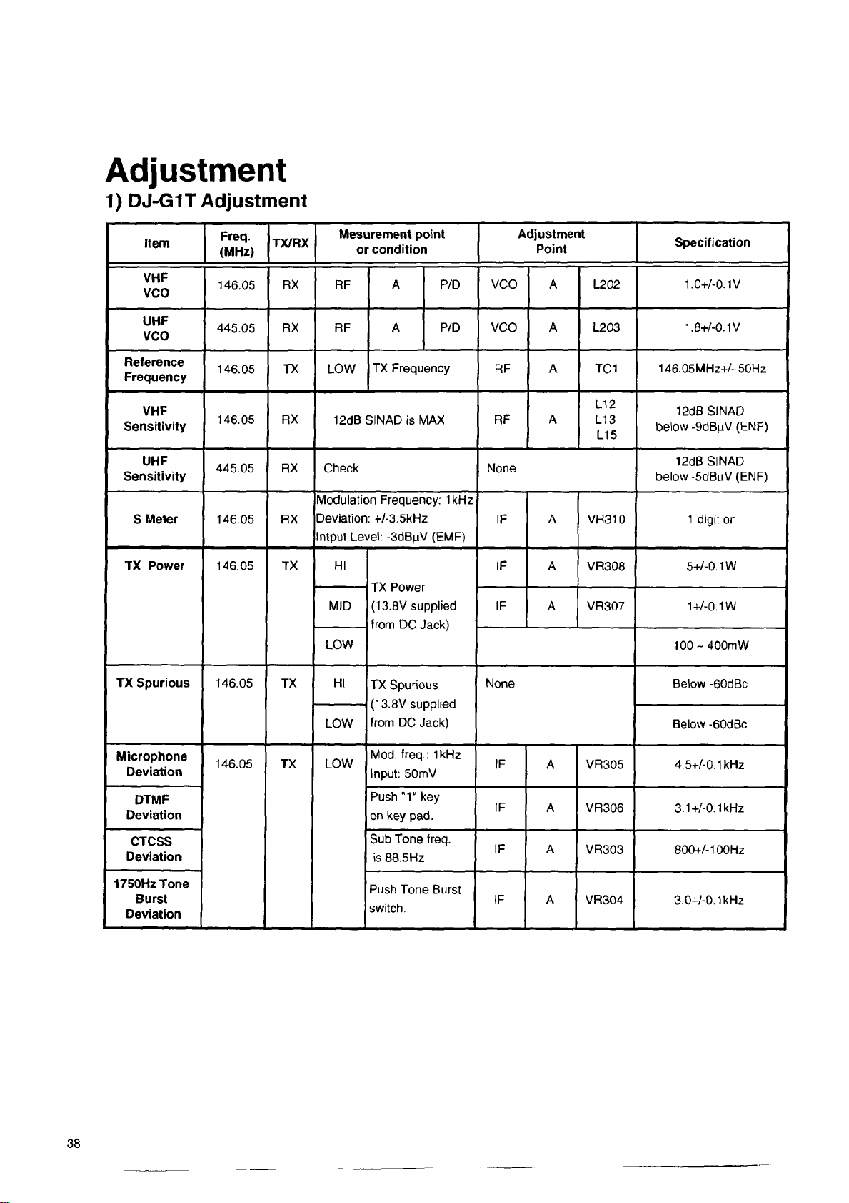
Adjustment
1) DJ- G 1 T A d ju st m e n t
Item
VHF
VCO
UHF
VCO
Reference
Frequency
VHF
Sensitivity
UHF
Sensitivity
S Meter
TX Power
Freq.
(MHz)
146.05
445.05
146.05
146.05
445.05
146.05
146.05 TX
TX/RX
RX RF
RX
RX Check
RX
Mesurement point
or condition
RX RF A P/D VCO
A
TX
LOW
Modulation Frequency: 1kHz
Deviation: +/-3.5kHz
Intput Level: -3dB|jV (EMF)
LOW
TX Frequency
12dB SINAD is MAX
HI
TX Power
(13.8V supplied
MID
from DC Jack)
P/D
VCO
RF A
RF A
None
IF A
IF A
IF
Adjustment
Point
A L202
A
A VR307 1+/-0.1W
L203
TC1
L12
L13
L15
VR310 1 digit on
VR308
146.05MHz+/-50Hz
below -9dBpV (ENF)
below -5dB^V (ENF)
Specification
1.0+/-0.1V
1.8+/-0.1V
12dB SINAD
12dB SINAD
5+/-0.1W
100- 400mW
TX Spurious
Microphone
Deviation
DTMF
Deviation
CTCSS
Deviation
1750Hz Tone
Burst
Deviation
146.05 TX
146.05 TX LOW
HI
LOW
TX Spurious
(13.8V supplied
from DC Jack)
Mod. freq.: 1kHz
Input: 50mV
Push "1“ key
on key pad.
Sub Tone freq.
is 88.5Hz
Push Tone Burst
switch.
None
IF
IF
IF A
IF A VR304
A
VR305 4.5+/-0.1kHz
A
VR306 3.1+/-0.1kHz
VR303 800+/-100Hz
Below -60dBc
Below -60dBc
3.0+/-0.1kHz
38
Page 43

2) DJ-G1E Adjustment
Item
VHF
VCO
UHF
VCO
Reference
Frequency
VHF
Sensitivity
UHF
Sensitivity
S Meter
TX Power 145.05
Freq.
(MHz)
145.05
433.05 RX RF
145.05
145.05
433.05 RX Check
145.05 RX
TX/RX
RX RF
TX
RX 12dB SIN AD is MAX RF A
TX
Mesurement point
or condition
A
A
LOW
Modulation Frequency: 1kHz
Deviation: +/-3.5kHz
Intput Level: -3dBnV (EMF)
MID IF
LOW
TX Frequency
HI
TX Power
(13.8V supplied
from DC Jack)
P/D
P/D VCO A
Adjustment
VCO
RF
None
IF
IF
Point
A
A
A
A
A VR307
L202
L203
TC1
L12
L13
VR310 1 digit on
VR308 5+/-0.1W
L15
Specification
0.9+/-0.1 V
1.4+/-0.1V
145.05MHZ+/- 50Hz
12dB SINAD
below -9dB|iV (ENF)
12dB SINAD
below -5dB|xV (ENF)
1+/-0.1W
100- 400mW
TX Spurious
Microphone
Deviation
DTMF
Deviation
CTCSS
Deviation
1750Hz Tone
Burst
Deviation
145.05 TX
145.05 TX
HI
LOW
LOW
TX Spurious
(13.8V supplied
from DC Jack)
Mod. freq.: 1kHz
Input: 50mV
Push "1" key
on key pad.
Sub Tone freq.
is 88.5Hz.
Push Tone Burst
switch.
None
IF
IF
IF
IF
Below -60dBc
Below -60dBc
A
VR305 4.5+/-0.1kHz
A VR306 3.1+/-0.1kHz
A
VR303 800+/-100Hz
A VR304
3.0+/-0.1kHz
Page 44

3) A d j u s tmen t Point s
IF Unit
RF Unit
3 ( • )
VR 306
V.
CZ Z)
VR 30 5
I--» .
o
d=t
a
VR 303
P I
= F t
= F t
VR 30 7
o
VR 30 8
1
40
Page 45

P C BOA RD VIEW
1) RF U n it S i de A
•; • ' ...
jk i ;.
mic ja c k ; ; ,
; 102-0 i- 540
i
>JK2„ ? '
SPJflCK '
HF>.il-i93-01-di0 :
1
UP0237 DJG10 RF-IF Flexible PCB
■ i24 -(r)
rc ts s.1 ^ L i15':.}
2P1 (E)
LEllJ
loW1
ici
M67748L
41
Page 46

4^
ro
2) RF Uni t Side B
Page 47

3) IF Unit Side A
TBS?]:
BRPf ¡120.1 W
UN9111
UP0237 RF-IF Flexible PCB
43
Page 48

4) IF Unit Side B
Page 49

5) CPU Unit Side A
CPU-IF Flexible PCB
-- -- -- ----- -- -- ----- -- -- ----- -- -- -- ----- -- -- ----- -- -- ----- -- -- ----- -- -- -- ----- -- -- --
--- ----
-----------------
1 > u?
2RZ^/7V 223 1/J/1SV
PTT PCB
45
Page 50

6) CPU Unit Side B
PTTPCB
^Jj4iKfey” ffle^ible'PCB
UP0236 CPU-1F Flex.
Page 51

7) VCO Unit
Side A
RF OlfT :
MOO
3. '.
C M
J:
< » > 1
<o
N
T
C O
L J
C M
1 &2CP. 1«o
CM
123 r.
i P-H.-l i
020
102
IQ
SideB
47
Page 52

8) KEY UNIT
9) Cha r ge U N I T
sari
f —i
JTmmmJ
UH
10 ) PT T UNIT
S501-S504
UU00Î5
SKOD-901
Page 53

2 S ü ÿ î & Q
<« o a a <« s S ! I » I § I ? S a í t i î s 9 I
mTTTTTmTTTÏÏTÏÏTTT^
UNO dU U
l A J V d O V I Q 0 I ± V I / \ I 3 H 0 S
Page 54

IF UNIT
8SB| i * * psa gg|'g!lB,,sssss I
Ly-< H H >-< M H H >-<>-< H ^
S oev
» V x - .
T w «
Page 55

3) CPU Unit
Page 56
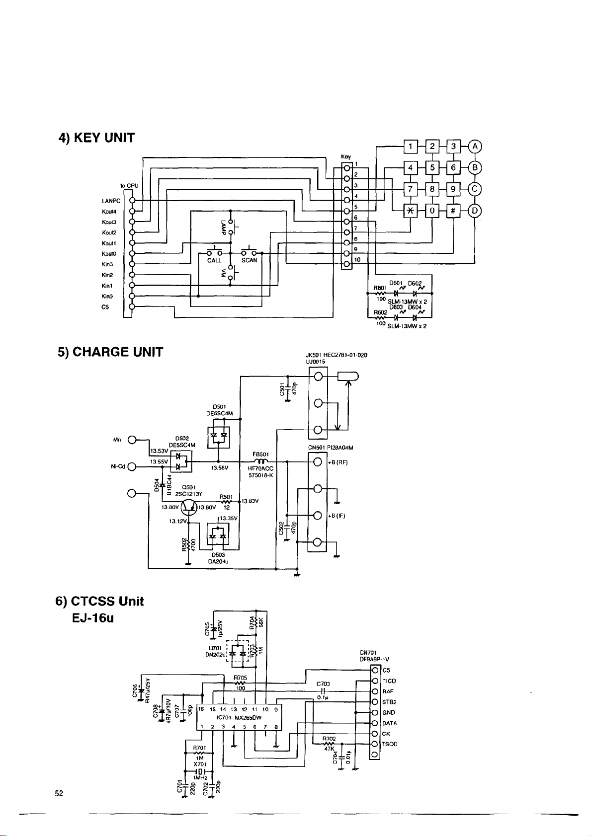
4) KEY UNIT
1
4
-H
I
7
I
I
*
□601 D602
R601 r f
1®° SLM-13MW X 2
D603 D604
R602 „rt
■vw—W
----H----
,0 0 S L M I3 M W X2
2
I
I
5L6
I
8
1 ■
1
0I.#
3
1
1
9
1
5 ) C HA RG E U NIT JK501 H ËC27BI-01-0 20
UJ0015
6) C TCSS Un i t
EJ - 16 U
52
Page 57

A F AMP (AM)
BLOCK DIAG RAM
Page 58

ES A L I N CO E L EC TR ON I CS I NC .
Head Office: "TWIN 21" MID Tower Building 23F
1-61, 2-Chome, Shiromi, Chuo-ku, Osaka No. 540, Japan
PHONE: 06-946-8150 FAX: 06-946-8175
USA: ALINCO ELECTRONICS INC.
438 Amapola Avenue, Unit 130, Torrance, CA 90501,U.S.A.
PHONE: 310-618-8616 FAX: 310-618-8758
Germany: ALINCO ELECTRONICS GMBH
Alt Hausen 34, D-60488 Frankfurt am Main, Germany
PHONE: 069-786018 FAX: 069-789-60766
Italy: ALINCO ELECTRONICS S.R.L.
Via Straffora, 35/D, 20090 Opera (Milano), Italy
PHONE: 02-57605160 FAX: 02-57606091
China: ALINCO ELECTRONICS (Beijing Office)
Beijing Fortune Bldg. Room 918-A
No.5 Dong San Huan Bei Lu, Chaoyang District Beijing China
PHONE: 01-501-7561 FAX: 01-501-7560
Printed in Japan
Dealer/Distributor
PM0024 rh 0194 A
 Loading...