

Page 1

LCD Monitor
Service Manual
Page 2

-2 -
MODEL:
LCT-17HT
Model No.: LCT-17HT
Version: 1.0
Page 3

-3 -
CONTENTS
SPECIFICATION..................................................................................................................................... 4
PANEL: HT17E12-200 ............................................................................................................................ 5
8 BIT MTP MICROCONTROLLER ..................................................................................................... 27
T0947 SCALER IC FPR XGA/SXGA LCD MONITORS .................................................................... 63
BLOCK DIAGRAM ............................................................................................................................ 184
TV TUNER .......................................................................................................................................... 185
EXPLODED VIEW & PART LIST...................................................................................................... 186
Model No.: LCT-17HT
Version: 1.0
Page 4

-4 -
SPECIFICATION
Resolution: 17.0 inch SXGA (1280 x 1024 @75Hz)
Color display: 16,777,216 colors
DPMS (Display Power Management Signaling)
OSD (On Screen Display)
Auto Configuration: Hot Key
Speaker [L + R: 3W + 3W = 6W (max)]
DDC 1/2 B: Plug & Play
Model No.: LCT-17HT
Version: 1.0
Page 5
-5 -
PANEL: HT17E12-200
1. GENERAL DESCRIPTION
1.1 Introduction
HT17E12-200 is a color active matrix TFT LCD module using amorphous silicon TFT's (Thin Film
Transistors) as an active switching devices. This module has a 17.0 inch diagonally measured active area
with SXGA resolutions (1280 horizontal by 1024 vertical pixel array). Each pixel is divided into RED,
GREEN, BLUE dots which are arranged in vertical stripe and this module can display 16,194,227 colors.
The TFT-LCD panel used for this module is adapted for a low reflection and higher color type.
1.2 Features
LVDS Interface with 2 pixel / clock
High-speed response
Low power consumption
6-bit (FRC) color depth, display 16,194,227 colors
Incorporated edge type back-light (Four lamps)
High luminance and contrast ratio, low reflection and wide viewing angle
DE (Data Enable) mode
Model No.: LCT-17HT
Version: 1.0
Page 6
-6 -
1.3 Applications
Desktop Type of PC & Workstation Use
Slim-Size Display for Stand-alone Monitor
Display Terminals for Control System
Monitors for Process Controller
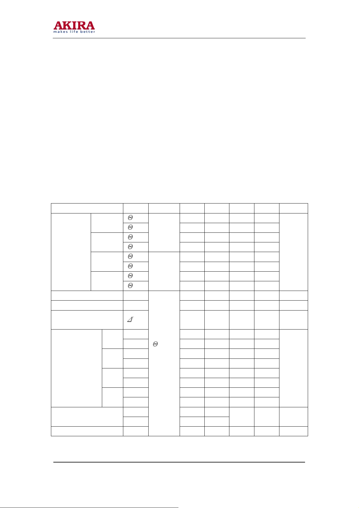
1.4 General Specifications
The followings are general specifications at the model HT17E12-200
<Table 1. General Specifications>
Parameter Specification Unit
Active area
Number of pixels
Pixel pitch
Pixel arrangement RGB Vertical stripe
Display colors 16,194,227 colors
Display mode Normally White
Dimensional outline
Weight 1900 max. gram
Back-light Top/Bottom edge side 4-CCFL type
Note: 1. CCFL (Cold Cathode Fluorescent Lamp)
Model No.: LCT-17HT
Version: 1.0
337.92 (H) × 270.336(V)
1280(H) × 1024(V)
0.264(H) × 0.264(V)
358.5(H) × 296.5(V) × 17.0(D) type
Mm
pixels
Mm
Mm
Page 7
-7 -
2.0 ABSOLUTE MAXIMUM RATINGS
The followings are maximum values which, if exceed, may cause faulty operation or damage to the unit.
The operational and non-operational maximum voltage and current values are listed in Table 2.
<Table 2. Absolute Maximum Ratings> [VSS = GND =0V]
Parameter Symbol Min Max Unit Remarks
Power Input Voltage VDD VSS-0.5 6.5 V
Logic Input Voltage VIN VSS-0.3 VDD+0.3 V
Back-light Lamp Current IBL 3 7 mA
Back-light lamp
Frequency
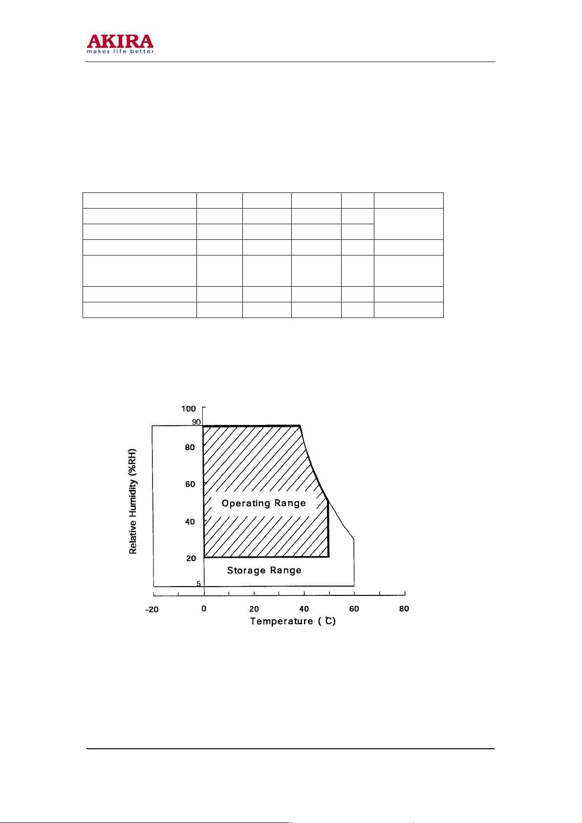
Operating Temperature TOP 0 +50 oC 1)
Storage Temperature TST -20 +60 oC 1)
Notes:
1. Temperature and relative humidity range are shown in the figure below.
2. Wet bulb temperature should be 39
FL 30 (80) KHz
o
C max and no condensation of water.
Ta=25
o
C
Model No.: LCT-17HT
Version: 1.0
Page 8
-8 -
3.0 ELECTRICAL SPECIFICATIONS
o
< Table 3. Electrical specifications > [Ta = 25±2
Parameter Min Typ Max Unit Remarks
Power Supply Voltage VDD 4.5 5.0 5.5 V
Power Supply Current IDD - 580 700 mA
Permissible Input Ripple
Voltage
High Level Differential Input
Threshold Voltage
Low Level Differential Input
Threshold Voltage
Back-light Lamp Voltage VBL 690 700 840 V
Back-light Lamp Current IBL 3.0 6.5 7.0 mA
Back-light Lamp operating
Frequency
Lamp Start Voltage
Lamp Life 40000 50000 hrs IBL = 6.5mA
Power Consumption
Notes:
1. The supply voltage is measured and specified at the interface connector of LCM. The current draw
and power consumption specified is for VDD = 5.0V, Frame rate= 75Hz and Clock frequency =
67.5MHz. Test Pattern of power supply current
a. Typ: Black pattern
b. Max: Dot pattern
2. The lamp frequency should be selected as different as possible from the horizontal synchronous
frequency and its harmonics to avoid interference, which may cause line flow on the display
3. The voltage above this value should be applied to the lamps for more than 1 second to start-up.
Otherwise the lamps may not be turned on.
4. Calculated value for reference (V
Model No.: LCT-17HT
Version: 1.0
VRF 100 mV VDD = 5.0V
VIH - +100 mV
VIL -100 - mV
FL 30 - 70 KHz Note 2
PD 2.9 W
PBL 18.2 W
P
21.1 W
total
× IBL) × 4 excluding inverter loss.
BL
C]
940 1170 V
1340 1570 V
Note1
Vcm
= 1.2V typ
rms
rms
25oC, Note 3
rms
0oC, Note 3
rms
= 6.5mA,
I
BL
Note 4
Page 9
-9 -
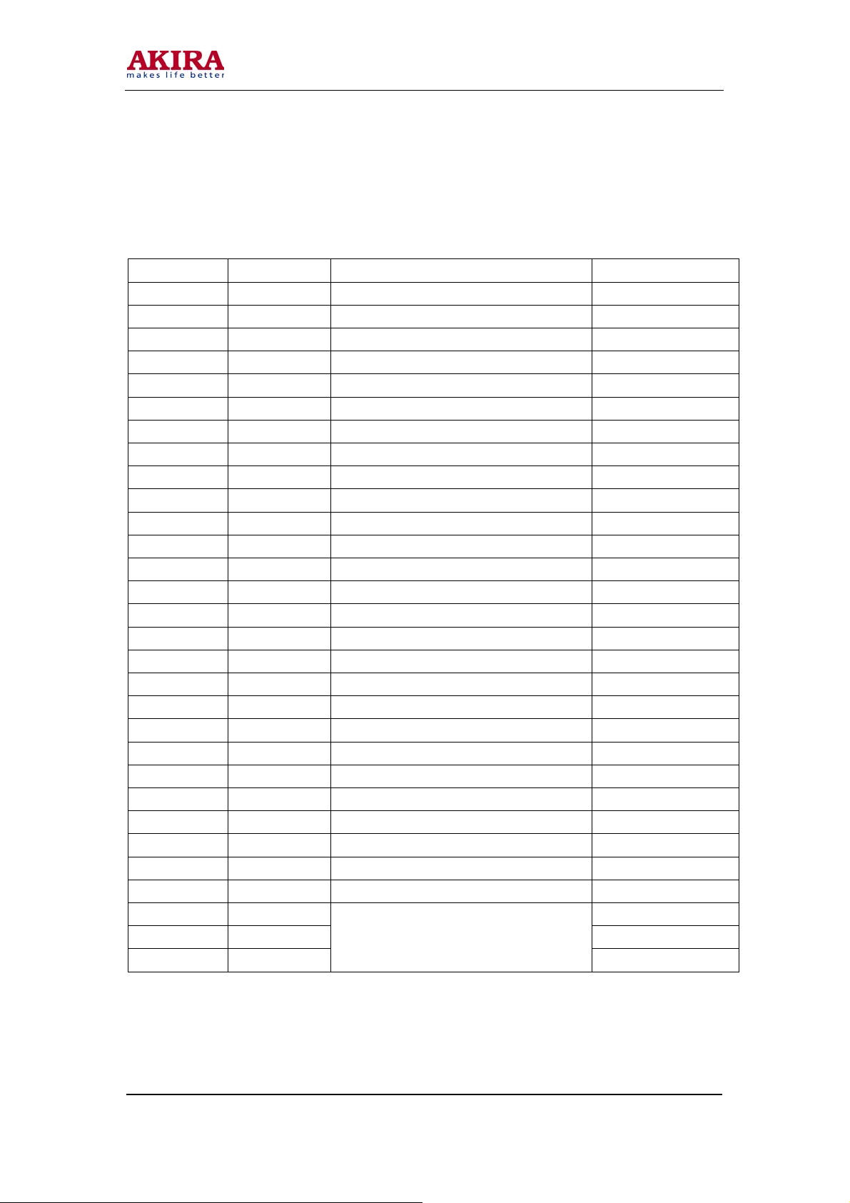
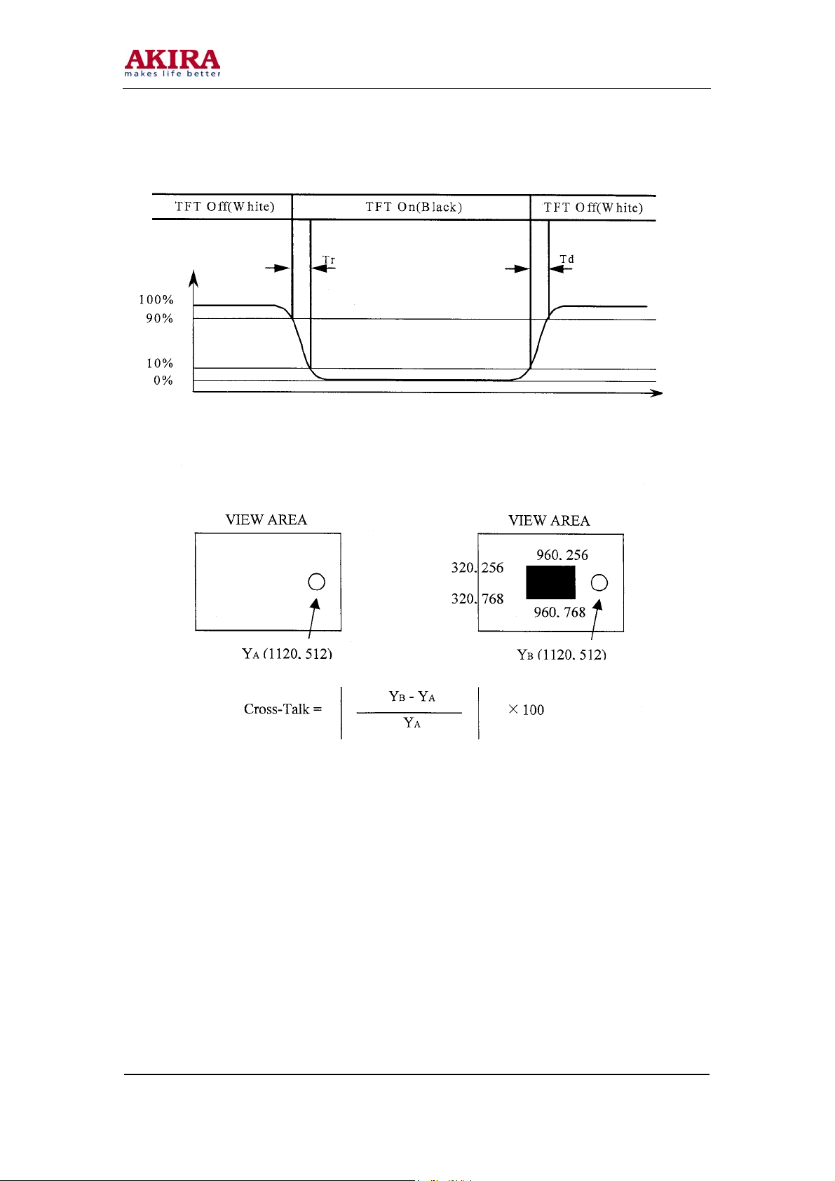
4.0 OPTICAL SPECIFICATIONS
4.1 Overview
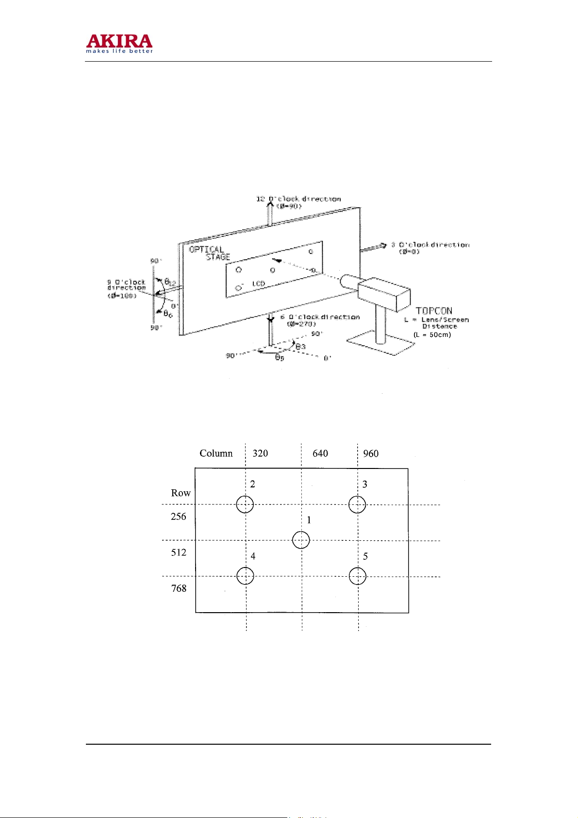
The test of Optical specifications shall be measured in a dark room (ambient luminance ≤ 1 lux and
temperature = 25±2°C) with the equipment of Luminance meter system (Goniometer system and
TOPCON BM-5) and test unit shall be located at an approximate distance 50cm from the LCD surface at
a viewing angle of θ and φ equal to 0°. We refer to θφ=0 (=θ3) as the 3 o’clock direction (the “right”),
θφ=90 (=θ12) as the 12 o’clock direction (“upward”), θφ=180 (=θ9) as the 9 o’clock direction (“left”)
and θφ=270 (=θ6) as the 6 o’clock direction (“bottom”). While scanning θ and/or φ, the center of the
measuring spot on the display surface shall stay fixed. The measurement shall be executed after 30
minutes warm-up period. VDD shall be 5.0V +/- 10% at 25°C. Optimum viewing angle direction is 6
o’clock.
4.2 Optical Specifications
[VDD=5.0V, Frame rate=60Hz, Clock=54MHz, IBL = 6.5mA, Ta = 25±2℃]
Parameter Symbol Condition Min Typ Max Unit Remark
Horizontal
Viewing
Angle
Luminance contrast ratio CR 350 430 - Note 2
Luminance of white YW 200 250 - cd/m2 Note 3
White luminance
uniformity
Reproduction
of color
Response time
Cross talk CT
Vertical
Horizontal
Vertical
White
Red
Green
Blue
3
9
12
6
3
9
12
6
Wx 0.270 0.300 0.330
Wy 0.305 0.335 0.365
Rx 0.599 0.629 0.659
Ry 0.324 0.354 0.384
Gx 0.257 0.287 0.317
Gy 0.568 0.598 0.628
Bx 0.115 0.145 0.175
By 0.073 0.103 0.133
Tr - 5
Td - 15
Y
CR>10
CR>5
o
=0
(Center)
Normal
Viewing
Angle
75 80 - Deg
75 80 - Deg
60 65 - Deg
60 65 - Deg
80 85 - Deg
80 85 - Deg
70 75 - Deg
70 75 - Deg
- - 1.2 Note 4
30 msec Note 6
- - 2.0 % Note 7
Note 1
Note 5
Model No.: LCT-17HT
Version: 1.0
Page 10

-10 -
Note:
1. Viewing angle is the angle at which the contrast ratio is greater than 10. The viewing are determined
for the horizontal or 3, 9 o’clock direction and the vertical or 6, 12 o’clock direction with respect to
the optical axis which is normal to the LCD surface.
2. Contrast measurements shall be made at viewing angle of θ= 0° and at the center of the LCD surface.
Luminance shall be measured with all pixels in the view field set first to white, then to the dark
(black) state. (See FIGURE 1 shown in Appendix) Luminance Contrast Ratio (CR) is defined
mathematically.
CR = Luminance when displaying a white raster
Luminance when displaying a black raster
3. Center Luminance of white is defined as the LCD surface. Luminance shall be measured with all
pixels in the view field set first to white. This measurement shall be taken at the locations shown in
FIGURE 2 for a total of the measurements per display.
4. The White luminance uniformity on LCD surface is then expressed as :
Luminance of five points / Minimum Luminance of five points (See FIGURE 2 shown in appendix).
5. The color chromaticity coordinates specified in Table 4. shall be calculated from the spectral data
measured with all pixels first in red, green, blue and white. Measurements shall be made at the center
of the panel.
6. The electro-optical response time measurements shall be made as FIGURE 3 shown in Appendix by
switching the “data” input signal ON and OFF. The times needed for the luminance to change from
10% to 90% is Td, and 90% to 10% is Tr.
7. Cross-Talk of one area of the LCD surface by another shall be measured by comparing the
luminance (Y
(Y
) of that same area when any adjacent area is driven dark. (See FIGURE 4 shown in Appendix).
B
) of a 25mm diameter area, with all display pixels set to a gray level, to the luminance
A
Y = Maximum
Model No.: LCT-17HT
Version: 1.0
Page 11
-11 -
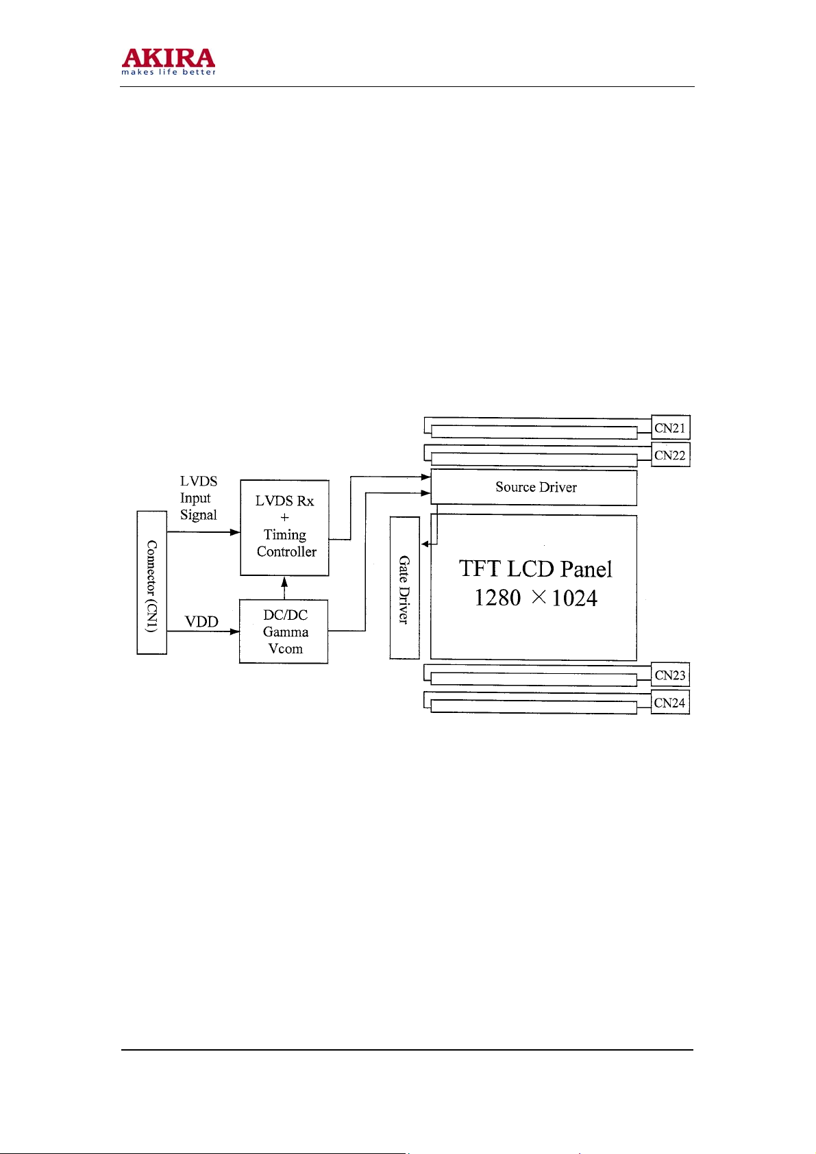
5.0 INTERFACE CONNECTION
5.1 Electrical Interface Connection
CN11: Module Side Connector : FI-XB30S-HF (JAE) or Equivalent
User Side Connector : FI-X30H-HF (JAE) or equivalent
Pin No Symbol Function Remark
1 RXO0- LVDS ODD 0 – SIGNAL
2 RXO0+ LVDS ODD 0 + SIGNAL
3 RXO1- LVDS ODD 1 – SIGNAL
4 RXO1+ LVDS ODD 1 + SIGNAL
5 RXO2- LVDS ODD 2 – SIGNAL
6 RXO2+ LVDS ODD 2 + SIGNAL
7 GND GROUND
8 RXOCLK- LVDS ODD CLOCK – SIGNAL
9 RXOCLK+ LVDS ODD CLCOK + SIGNAL
10 RXO3- LVDS ODD 3 – SIGNAL
11 RXO3+ LVDS ODD 3 + SIGNAL
12 RXE0- LVDS EVEN 0 – SIGNAL
13 RXE0+ LVDS EVEN 0 + SIGNAL
14 GND GROUND
15 RXE1- LVDS EVEN 1 – SIGNAL
16 RXE1+ LVDS EVEN 1 + SIGNAL
17 GND GROUND
18 RXE2- LVDS EVEN 2 – SIGNAL
19 RXE2+ LVDS EVEN 2 + SIGNAL
20 RXECLK- LVDS EVEN CLOCK – SIGNAL
21 RXECLK+ LVDS EVEN CLOCK + SIGNAL
22 RXE3- LVDS EVEN 3 – SIGNAL
23 RXE3+ LVDS EVEN 3 + SIGNAL
24 GND GROUND
25 NC NO CONECTION
26 DE NO CONECTION
27 NC NO CONECTION
28 VDD
29 VDD
30 VDD
POWER SUPPLY (+5.0V)
Model No.: LCT-17HT
Version: 1.0
Page 12
-12 -
5.2 LVDS Interface (Tx: THC63LVDF83A or Equivalent)
Input signal Transmitter Interface FI-X30S-HF Remark
Pin No Pin No System (Tx) TFT-LCD (Rx) Pin No.
OR0 51
OR1 52
OR2 54
OR3 55
OR4 56
OR5 3
OG0 4
OG1 6
OG2 7
OG3 11
OG4 12
OG5 14
OB0 15
OB1 19
OB2 20
OB3 22
ODD LVDS
OB4 23
OB5 24
HSYNC 27
VSYNC 28
DE 30
MCLK 31 40
OR6 50
OR7 2
OG6 8
OG7 10
OB6 16
OB7 18
RSVD 25
ER0 51
ER1 52
ER2 54
ER3 55
ER4 56
EVEN LVDS
ER5 3
EG0 4
48
47
46
45
42
41
39
38
37
48
47
OUT0-
OUT0+
OUT1-
OUT1+
OUT2-
OUT2+
CLKOUT-
CLKOUT+
OUT3+
OUT3-
OUT0-
OUT0+
RXO0-
RXO0+
RXO1-
RXO1+
RXO2-
RXO2+
RXO CLK-
RXO CLK+
RXO3-
RXO3+
RXE0-
RXE0+
1
2
3
4
5
6
8
9
10
11
12
13
Model No.: LCT-17HT
Version: 1.0
Page 13
-13 -
Input signal Transmitter Interface FI-X30S-HF Remark
Pin No Pin No System (Tx) TFT-LCD (Rx) Pin No.
EG1 6
EG2 7
EG3 11
EG4 12
EG5 14
EB0 15
EB1 19
EB2 20
EB3 22
EB4 23
EB5 24
HSYNC 27
VSYNC 28
EVEN LVDS
DE 30
MCLK 31
ER6 50
ER7 2
EG6 8
EG7 10
EB6 16
EB7 18
RSVD 25
46
45
42
41
40 CLKOUT- RXE CLK- 20
39 CLKOUT+ RXE CLK+ 21
38
37
OUT1-
OUT1+
OUT2 –
OUT2+
OUT3+
OUT3 -
RXE1-
RXE1+
RXE2-
RXE2+
RXE3-
RXE3+
15
16
18
19
22
23
Model No.: LCT-17HT
Version: 1.0
Page 14
(
)
(
)
(
)
(
)
-14 -
5.3 Data Input Format
ODD EVEN
5.4 Back-light Interface Connection
C
N21, 22, 23, 24: Module side connector : BHSR-02VS-1 (JST)
Pin No INPUT Color Function
1 HOT Pink & White High voltage
2 COLD Black & White Ground
(1,1) (2,1)
RGBRGB RGBRGB
1 Pixel = 3 Dots
RGB
RGBRGB RGBRGB
(1,1024) (2,1024)
Display Position of Input Data (V-H)
User side connector : SM02B-BHSS-1-TB (JST) or equivalent
Pin No INPUT Color Function
1279,1
1279,1024
1280,1
1280,1024
Model No.: LCT-17HT
Version: 1.0
Page 15
-15 -
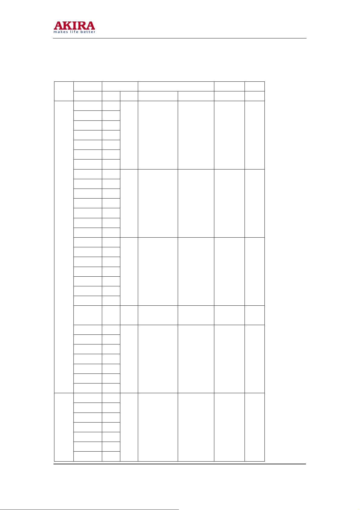
6.0 SIGNAL TIMING SPECIFICATION
6.1 The HT17E12-200 is operated by the only DE (Data enable) mode (LVDS Transmitter Input)
Item Symbols Min Typ Max Unit
Frequency 1/Tc 40 54 68 MHz
Clock
Data
Data Enable Setup Time Tes 4 - - ns
Vertical Display Period Tvd - 1024 - lines
One Line Scanning Period Th 672 844 1022 clocks
Horizontal Display Period Thd 640 640 640 clocks
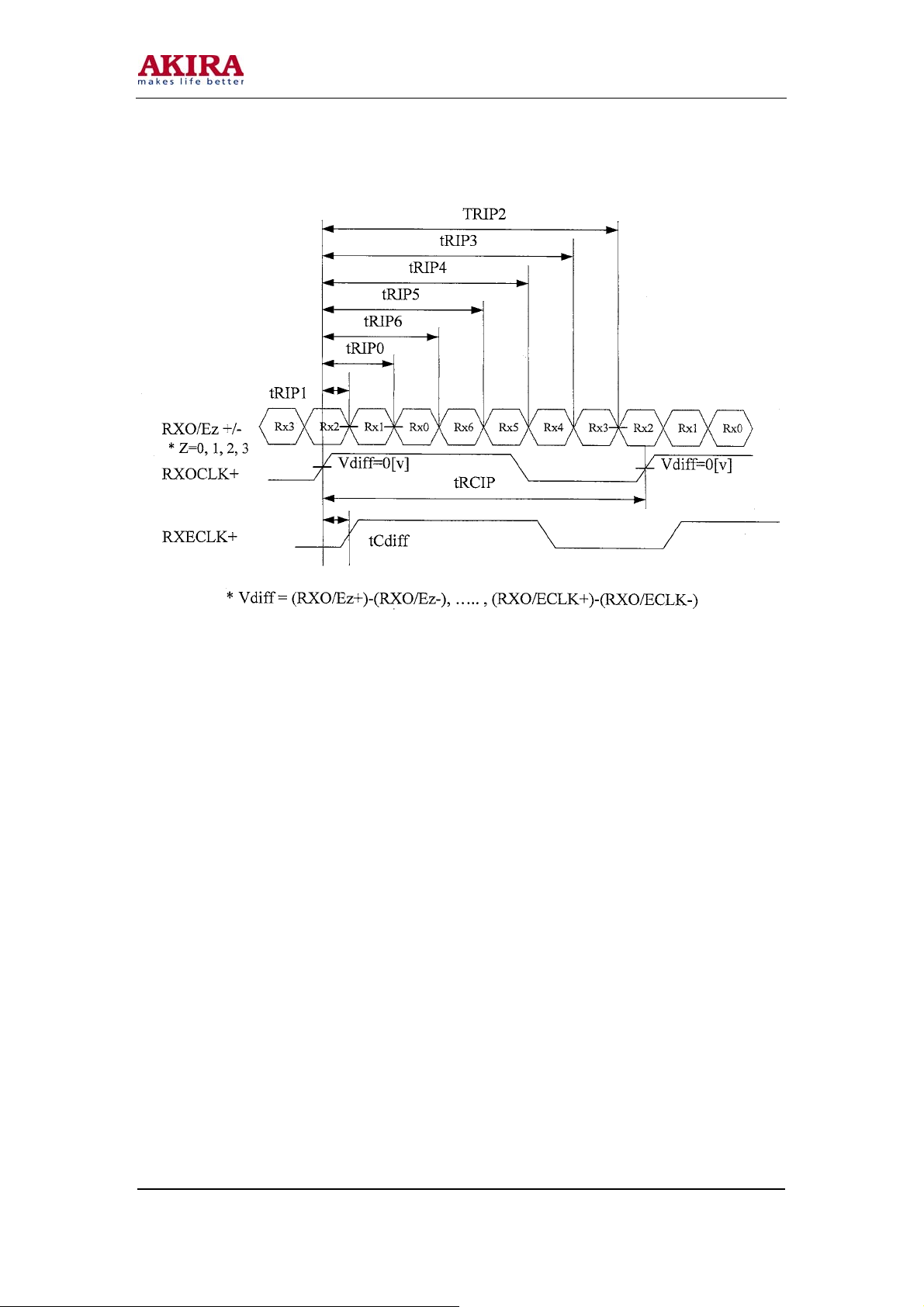
6.2 LVDS Rx interface timing parameter
The specification of the LVDS Rx interface timing parameter is shown in Table 4.
< Table 4. LVDS Rx Interface Timing Specification>
CLKIN Period tRCIP 14.7 18.5 - nsec
CLK Difference tCdiff -tRCIP*(3/7) 0 +tRCIP*(3/7) nsec
Input Data 0 tRIP1 -0.4 0 +0.4 nsec
Input Data 1 tRIP0 1*tRICP/7-0.4 1*tRICP/7 1*tRICP/7+0.4 nsec
Input Data 2 tRIP6 2*tRICP/7-0.4 2*tRICP/7 2*tRICP/7+0.4 nsec
Input Data 3 tRIP5 3*tRICP/7-0.4 3*tRICP/7 3*tRICP/7+0.4 nsec
Input Data 4 tRIP4 4*tRICP/7-0.4 4*tRICP/7 4*tRICP/7+0.4 nsec
Input Data 5 tRIP3 5*tRICP/7-0.4 5*tRICP/7 5*tRICP/7+0.4 nsec
Input Data 6 tRIP2 6*tRICP/7-0.4 6*tRICP/7 6*tRICP/7+0.4 nsec
High Time Tch 5 - - ns
Low Time Tcl 5 - - ns
Setup Time Tds 4 - - ns
Hold Time Tdh 4 - - ns
Frame Period
Item Symbol Min Typ Max Unit Remark
Tv 1032 1066 1536 lines
13.33 16.67 - msec
Model No.: LCT-17HT
Version: 1.0
Page 16
-16 -
Model No.: LCT-17HT
Version: 1.0
Page 17
-17 -
7.0 SIGNAL TIMING WAVEFORMS OF INTERFACE SIGNAL
7.1 Vertical timing waveforms
7.2 Horizontal Timing Waveforms
Model No.: LCT-17HT
Version: 1.0
Page 18
-18 -
8.0 INPUT SIGNAL, BASIC DISPLAY COLORS & GRAY SCALE OF COLOR
Red data Green data Blue data Colors & Gray
Scale
Black 0 0 0 0 0 0 0 0 0 0 0 0 0 0 0 0 0 0 0 0 0 0 0 0
Blue 0 0 0 0 0 0 0 0 0 0 0 0 0 0 0 0 1 1 1 1 1 1 1 1
Green 0 0 0 0 0 0 0 0 1 1 1 1 1 1 1 1 0 0 0 0 0 0 0 0
Cyan 0 0 0 0 0 0 0 0 1 1 1 1 1 1 1 1 1 1 1 1 1 1 1 1
Basic
Colors
Red 1 1 1 1 1 1 1 1 0 0 0 0 0 0 0 0 0 0 0 0 0 0 0 0
Magenta 1 1 1 1 1 1 1 1 0 0 0 0 0 0 0 0 0 0 1 1 1 1 1 1
Yellow 1 1 1 1 1 1 1 1 1 1 1 1 1 1 1 1 0 0 0 0 0 0 0 0
White 1 1 1 1 1 1 1 1 1 1 1 1 1 1 1 1 1 1 1 1 1 1 1 1
Black 0 0 0 0 0 0 0 0 0 0 0 0 0 0 0 0 0 0 0 0 0 0 0 0
Darker
Gray
Scale
Of Red
Brighter
Red 1 1 1 1 1 1 1 1 0 0 0 0 0 0 0 0 0 0 0 0 0 0 0 0
Black 0 0 0 0 0 0 0 0 0 0 0 0 0 0 0 0 0 0 0 0 0 0 0 0
Gray
Darker
Scale
Of
Green
Brighter
Green 0 0 0 0 0 0 0 0 1 1 1 1 1 1 1 1 0 0 0 0 0 0 0 0
Black 0 0 0 0 0 0 0 0 0 0 0 0 0 0 0 0 0 0 0 0 0 0 0 0
Gray
Darker
Scale
Of
Blue
Brighter
Blue 0 0 0 0 0 0 0 0 0 0 0 0 0 0 0 0 1 1 1 1 1 1 1 1
Black 0 0 0 0 0 0 0 0 0 0 0 0 0 0 0 0 0 0 0 0 0 0 0 0
Gray
Scale
Darker
Of
White
&
Brighter
Black
White 1 1 1 1 1 1 1 1 1 1 1 1 1 1 1 1 1 1 1 1 1 1 1 1
R7 R6 R5 R4 R3 R2 R1 R0 G7 G6 G5 G4 G3 G2 G1 G0 B7 B6 B5 B4 B3 B2 B1 B0
▲
0 0 0 0 0 0 0 1 0 0 0 0 0 0 0 0 0 0 0 0 0 0 0 0
0 0 0 0 0 0 1 0 0 0 0 0 0 0 0 0 0 0 0 0 0 0 0 0
▲
▼
1 1 1 1 1 1 0 1 0 0 0 0 0 0 0 0 0 0 0 0 0 0 0 0
▼
1 1 1 1 1 1 1 0 0 0 0 0 0 0 0 0 0 0 0 0 0 0 0 0
0 0 0 0 0 0 0 0 0 0 0 0 0 0 0 1 0 0 0 0 0 0 0 0
▲
0 0 0 0 0 0 0 0 0 0 0 0 0 0 1 0 0 0 0 0 0 0 0 0
▲
▼
0 0 0 0 0 0 0 0 1 1 1 1 1 1 0 1 0 0 0 0 0 0 0 0
▼
0 0 0 0 0 0 0 0 1 1 1 1 1 1 1 0 0 0 0 0 0 0 0 0
0 0 0 0 0 0 0 0 0 0 0 0 0 0 0 0 0 0 0 0 0 0 0 1
▲
0 0 0 0 0 0 0 0 0 0 0 0 0 0 0 0 0 0 0 0 0 0 1 0
▲
▼
0 0 0 0 0 0 0 0 0 0 0 0 0 0 0 0 1 1 1 1 1 1 0 1
▼
0 0 0 0 0 0 0 0 0 0 0 0 0 0 0 0 1 1 1 1 1 1 1 0
0 0 0 0 0 0 0 1 0 0 0 0 0 0 0 1 0 0 0 0 0 0 0 1
▲
0 0 0 0 0 0 1 0 0 0 0 0 0 0 1 0 0 0 0 0 0 0 1 0
▲
▼
1 1 1 1 1 1 0 1 1 1 1 1 1 1 0 1 1 1 1 1 1 1 0 1
▼
1 1 1 1 1 1 1 0 1 1 1 1 1 1 1 0 1 1 1 1 1 1 1 0
↑
↓
↑
↓
↑
↓
↑
↓
↑
↓
↑
↓
↑
↓
↑
↓
↑
↓
↑
↓
↑
↓
↑
↓
Model No.: LCT-17HT
Version: 1.0
Page 19
-19 -
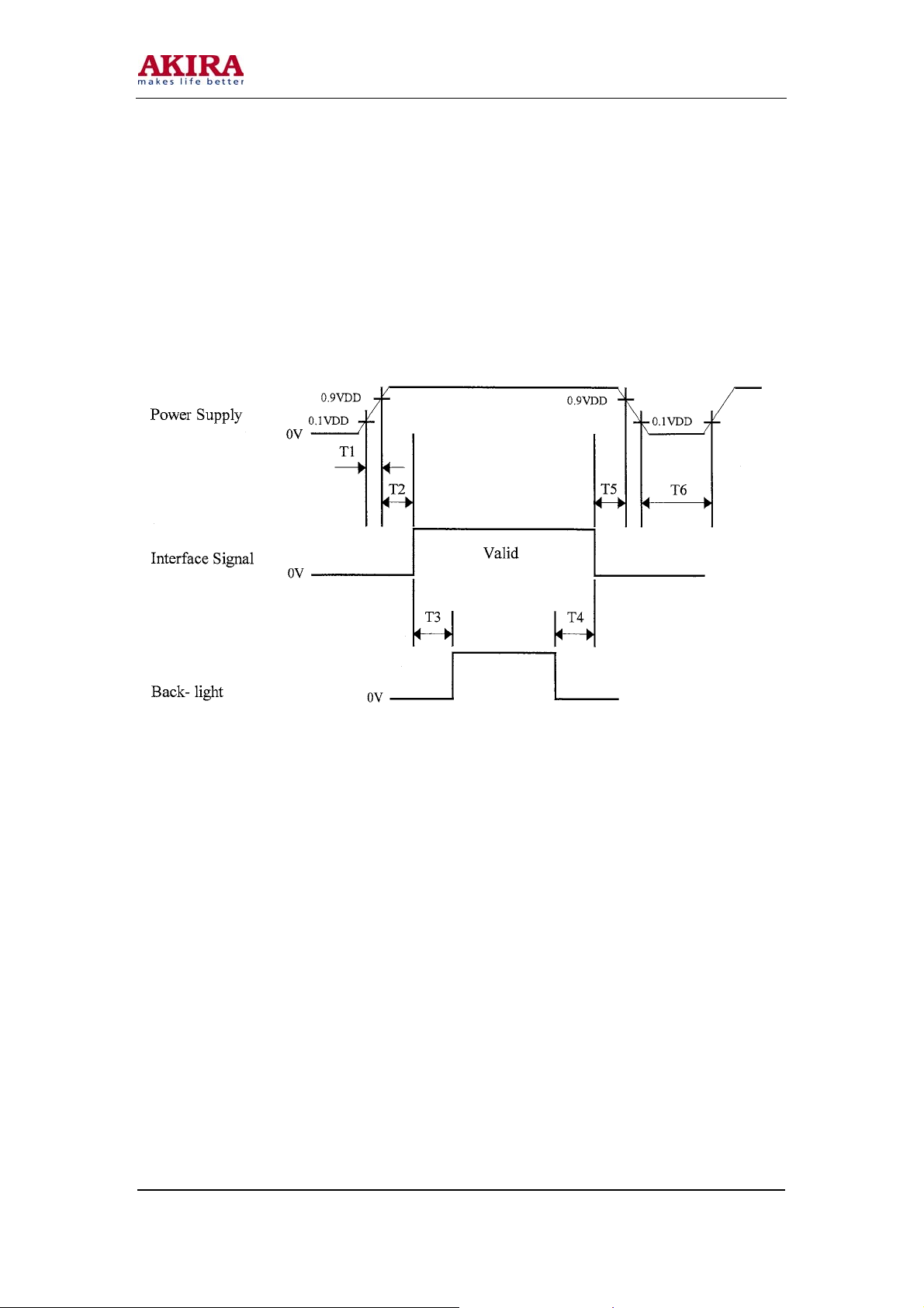
9.0 POWER SEQUENCE
To prevent a latch-up or DC operation of the LCD module, the power on/off sequence should be as
shown in below.
0 < T1 ≤ 10 ms
20ms < T2 ≤ 50 ms
500 ms ≤ T3
100 ms ≤ T4
0 < T5 ≤ 50 ms
1 sec ≤ T6
Notes:
1. When the power supply VDD is 0V, Keep the level of input signals on the low or keep high
impedance.
2. Do not keep the interface signal high impedance when power is on.
3. Back Light must be turn on after power for logic and interface signal are valid.
Model No.: LCT-17HT
Version: 1.0
Page 20

-20 -
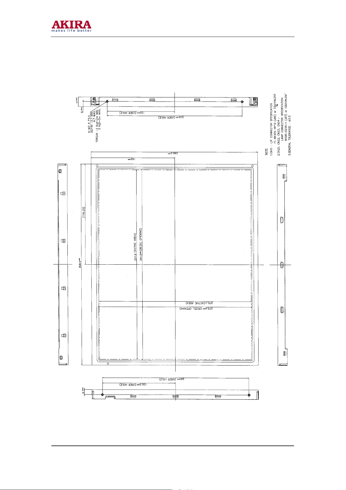
10.0 MECHANICAL CHARACTERSTICS
10.1 Dimensional Requirement
FIGURE 6 shown in appendix shows mechanical outlines for the model HT17E12-200. Other
parameter are shown in Table 5.
<Table 5. Dimensional Parameter>
Parameter Specification Unit
Dimensional outline
Horizontal 358.5 ± 0.5
Vertical 296.5 ± 0.5
Thickness 17.0 ± 0.5
Weight 1900 max Gram
Active area 337.92 (h) x 270.336 (v) Mm
Pixel pitch 0.264 (h) x 0.264 (v) Mm
Number of pixels 1280 (h) x 1024 (v) (1 pixel = R + G + B dot) Pixels
Back-light Top/bottom edge 4-CCFL type
10.2 Mounting
See FIGURE 5 shown in appendix
10.3 Anti-Glare and Polarizer Hardness.
The surface of the LCD has an anti-glare coating to minimize reflection and a coating to reduce
scratching.
10.4 Light Leakage
There shall not be visible light from the back-lighting system around the edges of the screen as seen from
a distance 50[cm] from the screen with an overhead light level of 350[lux].
The manufacture shall furnish limit samples of the panel showing the lightest leakage acceptable.
Model No.: LCT-17HT
Version: 1.0
Mm
Page 21
-21 -
11.0 RELIABILITY TEST
The Reliability test items and its conditions are shown in below.
<Table 6. Reliability Test Parameter>
No Test Items Conditions
1 High temperature storage test Ta = 60oC, 240 hrs
2 Low temperature storage test Ta = -20oC, 240 hrs
High temperature & high humidity operation
3
test
4 High temperature operation test Ta = 50oC, 240 hrs
5 Low temperature operation test Ta = 0oC, 240 hrs
6 Thermal shock Ta = -20oC ↔ 60oC (30 min), 100 cycle
7 Vibration test (non-operating)
8 Shock test (non-operating)
9 Electrostatic discharge test
Model No.: LCT-17HT
Version: 1.0
Ta = 50
Frequency : 10 ~ 300 Hz, Sweep rate 30min
Gravity/AMP : 1.5G
Period : ±X, ±Y, ±Z 30min
Gravity : 70G
Pulse width : 11ms, sine wave
Air : 150 pF, 330Ω, 15KV
Contact : 150 pF, 330Ω, 8KV
o
C, 80 %RH, 240 hrs
± X, ± Y, ± Z Once for each direction
Page 22

-22 -
12.0 HANDLING & CAUTIONS
12.1 Cautions when taking out the module
Pick the pouch only, when taking out module from a shipping package.
12.2 Cautions for handling the module
As the electrostatic discharges may break the LCD module, handle the LCD module with
care. Peel a protection sheet off from the LCD panel surface as slowly as possible.
As the LCD panel and back-light element are made from fragile glass material, impulse and
pressure to the LCD module should be avoided.
As the surface of the polarizer is very soft and easily scratched, use a soft dry-cloth without
chemicals for cleaning.
Do not pull the interface connector in or out while the LCD module is operating.
Put the module display side down on a flat horizontal plane.
Handle connectors and cables with care.
12.3 Cautions for the operation
When the module is operating, do not lose LVDS signals. If any one of these signals were
lost, the LCD panel would be damaged.
Obey the supply voltage sequence. If the wrong sequences were applied, the module would be
damaged.
12.4 Cautions for the atmosphere
Dewdrop atmosphere should be avoided.
Do not store and/or operate the LCD module in a high temperature and/or humidity
atmosphere. Storage in an electro-conductive polymer-packing pouch and under relatively
low temperature atmosphere is recommended.
12.5 Cautions for the module characteristics
Do not apply fixed pattern data signal to the LCD module at aging time.
Applying fixed pattern for a long time may cause image sticking.
12.6 Other cautions
Do not disassemble and/or re-assemble LCD module.
Do not re-adjust variable resistor or switch etc.
When returning the module for repair or etc, please pack the module not to be broken. We
recommend on using the original shipping packages.
Model No.: LCT-17HT
Version: 1.0
Page 23
-23 -
14.0 APPENDIX
Figure 1. Measurement Set Up
Figure 2. Average Luminance Measurement Locations & Uniformity Measurement Locations.
Model No.: LCT-17HT
Version: 1.0
Page 24
-24 -
Figure 3. Response Time Testing
Figure 4. Cross Modulation Test Description
Where:
= Initial luminance of measured area (cd/m2)
Y
A
= Subsequent luminance of measured area (cd/m2)
Y
B
The location measured will be exactly the same in both patterns.
Model No.: LCT-17HT
Version: 1.0
Page 25
-25 -
Figure 5. TFT-LCD Module Outline Dimensions (Front View)
Model No.: LCT-17HT
Version: 1.0
Page 26
-26 -
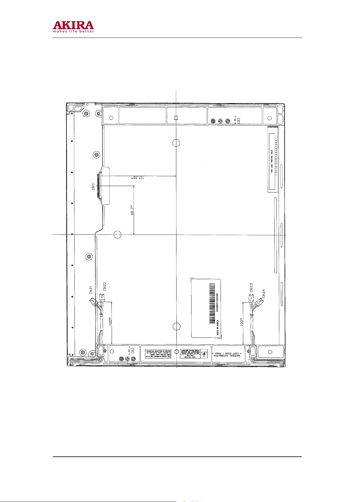
Figure 6. TFT-LCD Module Outline Dimensions (Rear view)
Model No.: LCT-17HT
Version: 1.0
Page 27

-27 -
8 BIT MTP MICROCONTROLLER
1.0 FEATURES
8051 instruction set compatible 8-bit microcontroller
8051/8052 compatible pinout
Complete static design, wide range of operation frequency from 1 ~ 40 MHz
Large on-chip memory
o 64K bytes built-in Multiple Times Programmable ROM (MTP-ROM) program
memory
o 512 bytes on-chip SRAM, expandable external 64K bytes address space
Dual Data Pointer
Four 8-bit bi-directional I/O ports
6 interrupts including 2 external sources
One full-duplex serial UART ports compatible with standard 8052
Three 16 bit timer/counters
On chip oscillator for crystal
Software Power-Down mode, supports Idle mode and Power Down mode for less power
consumption
ROM Code Protection
4.5V~5.5V operation voltage, 12V programming voltage
44-pin PLCC or QFP package
1.1 General Description
The M6759 is an 8032/8052 instruction compatible 8-bit microcontroller with MTP Flash ROM for
firmware updating. By combining a versatile 8-bit CPU with MTP-Flash, this device provides whole
microcontroller system on one chip and still remains the feasibility for general control systems in a
variety of applications. Furthermore, user-defined security registers can protect the firmware after
the code is ready.
The M6759 contains the following:
a. A non-volatile 64K bytes Multiple Times Programmable ROMprogram memory.
b. A volatile 512 bytes read/write data memory
c. Four 8-bit I/O ports, two 16-bit timer/event counters (identical to the timers of the 80C51)
d. A 16-bit timer (identical to the Timer 2 of the 8052).
e. A multi-source two-priority-level nested interrupt structure.
f. One serial interface (UART) and
g. An on-chip oscillator.
Model No.: LCT-17HT
Version: 1.0
Page 28
-28 -
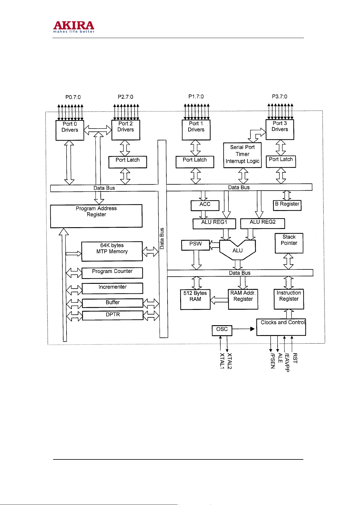
1.2 Block Diagram
Model No.: LCT-17HT
Version: 1.0
Page 29
-29 -
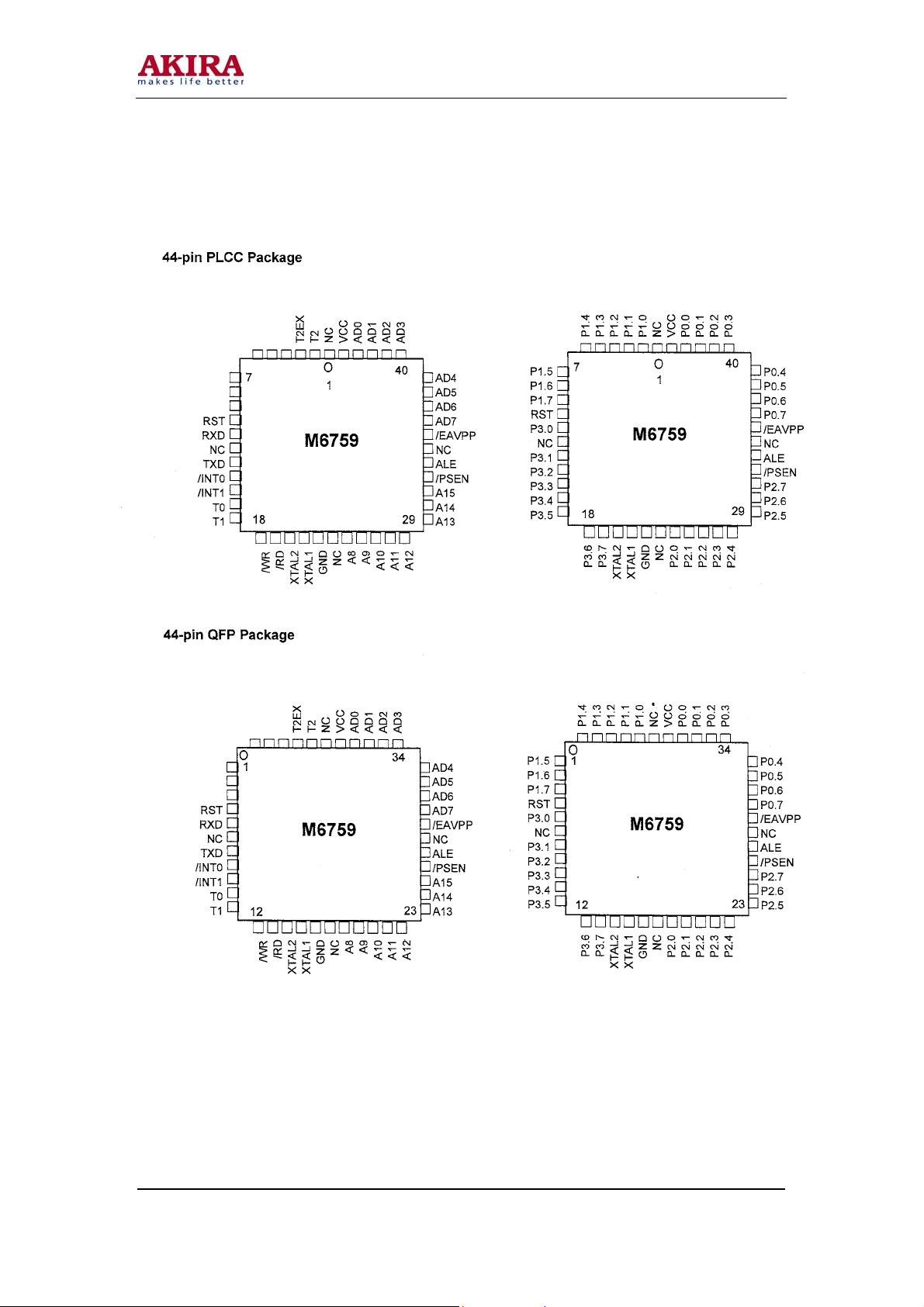
2.0 PIN Description
2.1 Pinout Diagram
Model No.: LCT-17HT
Version: 1.0
Page 30

-30 -
2.2 Pin Description Table
Pin assignments shown below are listed based on 44-pin PLCC package. And if not additionally
specified, further pin number reference throughout this datasheet is, by default, referred to 44-pin PLCC
package. As for the QFP package, the pin number assignment should be shifted accordingly, as
comparatively shown in Section 2.1 Pinout Diagram.
Pin Name No. (PLCC) Type Description
VDD 44 IN Power supply for internal operation, 5V input.
GND 22 IN Ground.
Port 0 is 8 bits bi-directional I/O port with internal pull high.
P0.7-P0.0
AD7-0
RST 10 IN
XTAL1 21 IN Crystal In, can be used as external clock input.
XTAL2 20 OUT Crystal out, feedback of XTAL1.
/PSEN 32 OUT
ALE 33 OUT Address Latch Enable, used to latch external LSB 8 bit address bus
P1.7-P1.0
T2EX
(P1.1)
T2 (P1.0)
P2.7-P2.0
A15-A8
36,37,38,39,
40,41,42, 43
9,8,7,6,5,4,3
,2
31,30,29,28,
27,26,25, 24
Multiplexed address/data bus. During the time when ALE is high, the
I/O
LSB of a memory address is presented. When ALE falls, the port
transitions to a bi-directional data bus. This bus is used to read external
ROM and read/write external RAM memory or peripherals.
Reset signal of internal circuit, it must be kept 4 clocks to ensure being
recognized by internal circuit. This signal will not affect internal
SRAM.
Program Store Enable Output, commonly connected to external ROM
memory as a chip enable during fetching and MOVC operation. /PSEN
goes high during a reset condition.
from multiplexed address/data bus, commonly connect to the latch
enable of 373 family. This signal will be forced high when the device is
in a reset condition.
Port 1 is 8 bits bi-directional I/O port with internal pull high. All pins
I/O
have an alternate function shown as below.
IN External timer/counter 2 trigger.
IN External timer/counter 2.
I/O Port 2 is 8 bits bi-directional I/O port with internal pull high. The
alternate function is MSB 8 bit address bus
OUT This bus emits the high-order address byte during fetches from external
Program Memory or during accesses to external Data Memory that use
16-bit addresses (MOVX @ DPTR).
During accesses to external Data Memory that use 8-bit addresses
(MOVX @ Ri), Port 2 emits the contents of the P2 Special Function
Register.
Model No.: LCT-17HT
Version: 1.0
Page 31

-31 -
P3.7-P3.0
/RD (P3.7)
/WR (P3.6)
T1 (P3.5)
T0 (P3.4)
/INT1
(P3.3)
/INT0
(P3.2)
TXD (P3.1)
RXD (P3.0)
/EAVPP 35 IN The pin must be externally held low to enable the device to fetch code
NC 1,12,23,34 NC These pins should not be connected for any purpose
Model No.: LCT-17HT
Version: 1.0
19,18,17,16,
15,14,13, 11
I/O Port 3 is an 8-bit bi-directional I/O port with internal pull high. The
reset condition of this port is with all bits at a logic 1.
Port 3 also have alternate function list below
OUT External data memory read strobe.
OUT External data memory write strobe.
IN External timer/counter 1.
IN External timer/counter 0.
IN External interrupt 1 (Negative Edge Detect).
IN External interrupt 0 (Negative Edge Detect).
OUT Serial port output.
IN Serial port input.
from external program memory. If /EAVPP is held high, the device
executes from internal program memory. /EAVPP is internal latched
on reset. This pin also receives the 12V programming voltage (V
during FLASH programming.
PP
)
Page 32

-32 -
3.0 FUNCTION DESCRIPTION
3.1 Data Space Addressing
The M6759 has internal data memory that is mapped into four separate segments: the lower 128 bytes of
RAM, upper 128 bytes of RAM, 128 bytes Special Function Register (SFR), and 256 bytes auxiliary
RAM (ARAM).
The four segments are:
a. The Lower 128 bytes of RAM (address 00H to 7FH) are directly and indirectly addressable.
b. The Upper 128 bytes of RAM (address 80H to FFH) are indirectly addressable only.
c. The Special Function Registers SFRs, (address 80H to FFH) are directly addressable only.
d. The 256-bytes auxiliary RAM (ARAM, 0000H-00FFH) are indirectly accessed by move external
instruction, MOVX.
Either direct or indirect addressing can access the lower 128 bytes. The upper 128 bytes can be accessed
by indirect address only. The upper 128 bytes occupy the same address space as the SFRs. That means
they have the same address, but are physically separate from SFR space.
The ARAM can be accessed by indirect addressing and MOVX instructions when ARAM_EN bit is set.
This part of memory is physically located on-chip, logically occupied the first 256-bytes of external data
memory if ARAM_EN bit is set.
The ARAM is indirectly addressed, using the MOVX instruction in combination with any of the registers
R0, R1 of the selected bank or DPTR. An access to ARAM will not affect ports P0, P3.6 (/WR) and P3.7
/RD).
If ARAM_EN is cleared, the access to external memory will be performed in the same way as standard
8051. If ARAM_EN is set and DPTR contains value lower than 0100H, the ARAM will be accessed
rather than external memory, but if DPTR contains value higher than 00FFH (i.e. 0100H to FFFFH), the
external memory will be accessed.
If ARAM_EN is set and P2 SFR contains 00H, the ARAM will be accessed by the MOVX @Ri, #data
instruction, but if P2 SFR contains a non-zero value, the external memory will be accessed using MOVX
@Ri, #data.
For example,
MOVX DPTR, #data
If ARAM_EN is set and DPTR contains 0030H, access the ARAM at address 030H rather than external
memory.
If ARAM_EN is set and DPTR contains 0130H, the external memory address 0130H will be accessed
Model No.: LCT-17HT
Version: 1.0
Page 33

-33 -
For example:
MOVX @R0, #data
If ARAM_EN is set, P2 SFR contains 00H, and R0 contains 30H, an access to the ARAM at address 30H
will be performed.
If ARAM_EN is set, P2 SFR contains 01H, and R0 contains 30H, an access to the external memory
address 0130H will be performed if P2 is connected to the high byte address bus of external RAM.
3.2 Dual Data Pointer
Data memory block moves can be accelerated using the Dual Data Pointer (DPTR). The standard 8051
DPTR is a 16-bit value that is used to address off-chip data RAM or peripherals. In the M6759, the
standard 16-bit data pointer is called DPTR0 and is located at SFR address 82H and 83H. These are the
standard locations. The new DPTR is located at SFR 84H and 85H and is called DPTR1. The new DPTR
Select bit (DPS) chooses the active pointer and is located at the LSB of the SFR location 86H. No other
bits in register 86H have any effect and are set to 0. The user switches between data pointer by toggling
the LSB of register 86H. The increment (INC) instruction is the fastest way to accomplish this. All
DPTR-related instructions use the currently selected DPTR for any activity.
3.3 Low EMI Mode
In normal operation ALE is emitted at a constant rate of 1/6 the oscillator frequency, and may be used for
external timing or clocking purpose. Note, however, that one ALE pulse is skipped during each access to
external Data Memory.
If desired, setting bit 0 of SFR location 8EH can disable ALE operation. With the bit set, ALE is active
only during a MOVX instruction. Otherwise the pin is weakly pulled high. Setting the ALE-disable bit
has no effect if the micro-controller is in external execution mode.
Model No.: LCT-17HT
Version: 1.0
Page 34

Memory Map
-34 -
Model No.: LCT-17HT
Version: 1.0
Page 35

-35 -
3.4 Idle Mode
In Idle mode, CPU put itself into sleep while all the on-chip peripherals remain active. The instruction
that sets PCON.0 is the last instruction executed in the normal operating mode before Idle mode is
activated. The content of RAM and special functions register remain unchanged, and the status of CPU
(includes Stack Point, Program Counter, Program Status Word and Accumulator) is preserved in this
mode.
There are two ways to terminate Idle mode:
Activation of any enabled interrupt will cause IDLE (PCON.0) to be cleared by hardware
terminating Idle mode. The interrupt will be serviced, and returned by instruction RETI. The
next instruction to be executed is the one which follows the instruction that wrote a logic 1 to
PCON.0. The flag bits GF0 (PCON.2) and GF3 (PCON.6) can be used to determine whether the
interrupt was received during normal execution or during the Idle mode. When Idle mode is
terminated by an interrupt, the service routine can examine the status of the flag bits.
The second way of terminating the Idle mode is with an external hardware reset.
3.5 Power Down Mode
Setting PCON.1 (PD) can force CPU enter Power Down mode. In this mode, on-chip oscillator is
stopped to save most of power. All functions are stopped due to the clock frozen, but the contents of
RAM and special functions register are held.
To terminate Power Down mode, the only way is hardware reset. Reset redefines the SFRs but does not
change the on-chip RAM. The reset should not be activated before VCC is restored to its normal
operating level and must be held active long enough to allow the oscillator to restart stably.
3.6 Reset
The RST is the reset input, which is the input to a Schmitt Trigger. A reset is accomplished by holding the
RST pin high for at least four oscillator periods while the oscillator is running. The CPU responds by
generating an internal reset, with the timing shown in Reset Timing. The external reset signal is
synchronous to the internal clock. The port pins will maintain high by internal pull-ups for 205 oscillator
periods after RST pin goes low. While the RST pin is high, ALE and /PSEN are weakly pulled high.
After RST is pulled low, it will take about 205 oscillator periods for ALE and PSEN to start clocking. For
this reason, other devices can not be synchronized to the internal timings of the m6759. Driving the ALE
and /PSEN pins to 0 while reset is active could cause the device to go into an indeterminate state.
The internal reset algorithm writes 0s to all the SFRs except the port latches, the Stack Pointer, and
SBUF. The port latches are initialized to FFH, the Stack Pointer to 07H, and SBUF is indeterminate. The
internal RAM is not affected by reset. On power up the RAM content is indeterminate.
Model No.: LCT-17HT
Version: 1.0
Page 36

-36 -
3.7 Interrupt Processing
When an enabled interrupt occurs, the CPU vectors to the address of the interrupt service routine (ISR)
associated with that interrupt, as listed in Table 11. The CPU executes the ISR to completion unless
another interrupt of higher priority occurs. Each ISR ends with a RETI (return from interrupt) instruction.
After executing the RETI, the CPU returns to the next instruction that would have been executed if the
interrupt had not occurred.
An ISR can only be interrupted by a higher priority interrupt. That is, an ISR for a low-priority level
interrupt can only be interrupted by high-priority level interrupt. An ISR for a high-priority level cannot
be interrupted by any other interrupt.
M6759 always completes the instruction in progress before servicing an interrupt. If the instruction in
progress is RETI, or a write access to any of the IP or IE SFRs, M6759 completes one additional
instruction before servicing the interrupt.
3.8 Interrupt Masking
The EA bit in the IE SFR (IE.7) is a global enable for all interrupts. When EA=1, each interrupt is
enabled/masked by its individual enable bit. When EA=0, all interrupts are masked.
3.9 Interrupt Priorities
There are two stages of interrupt priority assignment, interrupt level and natural priority. The interrupt
level (high or low) takes precedence over natural priority. All interrupts can be assigned to be high or low
priority. In addition to an assigned priority level, each interrupt also has a natural priority, as listed in
Table 3-2. Simultaneous interrupts with the same priority level (for example, both high) are resolved
according to their natural priority. For example, if /INT0 and /INT1 are both programmed as high
priority, /INT0 takes precedence.
Once an interrupt is being serviced, only an interrupt of higher priority level can interrupt the service
routine of the interrupt currently being serviced.
Mode Program
Memory
Idle Internal 1 1 Data Data Data Data
Idle External 1 1 Float Data Address Data
Power Down Internal 0 0 Data Data Data Data
Power Down External 0 0 Float Data Data Data
Table 3-1. Status of the External pins During Idle and Power Down
ALE /PSEN Port0 Port1 Port2 Port3
Model No.: LCT-17HT
Version: 1.0
Page 37

Reset Timing
-37 -
Model No.: LCT-17HT
Version: 1.0
Page 38

-38 -
Table 3-2. Interrupt Natural Vectors and Priorities
Interrupt Description Natural Priority Interrupt Vector
/INT0 External interrupt 0 0 03H
TF0 Timer 0 interrupt 1 0BH
/INT1 External interrupt 1 2 13H
TF1 Timer 1 interrupt 3 1BH
TI or RI Serial Port transmit or receive interrupt 4 23H
TF2 Timer 2 interrupt 5 2BH
Table 3-3. Interrupt Flag, Enables and Priority Control
Interrupt Description Flag Enable Priority Control
/INT0 External interrupt 0 TCON.1 IE.0 IP.0
TF0 Timer 0 interrupt TCON.5 IE.1 IP.1
/INT1 External interrupt 1 TCON.3 IE.2 IP.2
TF1 Timer 1 interrupt TCON.7 IE.3 IP.3
TI or RI Serial Port transmit or receive interrupt
TF2 Timer 2 interrupt T2CON.7 IE.6 IP.6
Model No.: LCT-17HT
Version: 1.0
SCON0.0
SCON0.1
IE.5 IP.5
Page 39

-39 -
4.0 SPECIAL FUNCTION REGISTERS
SFR Register Map
Register Bit 7 Bit 6 Bit 5 Bit 4 Bit 3 Bit 2 Bit 1 Bit 0 Addr
P0 80H
SP 81H
DPL0 82H
DPH0 83H
DPL1 84H
DPH1 85H
DPS 0 0 0 0 0 0 0 SEL 86H
PCON SMOD GF4 GF3 GF2 GF1 GF0 STOP IDLE 87H
TCON TF1 TR1 TF0 TR0 IE1 IT1 IE0 IT0 88H
TMOD GATE C/T M1 M0 GATE C/T M1 M0 89H
TL0 8AH
TL1 8BH
TH0 8CH
TH1 8DH
LEMI 0 0 0 0 0 0 0 LOWEMI 8EH
P1 90H
AUXR ARAM_EN GF6 GF5 *EB *BRG1 *BRG0 *INT2I *INT2E 97H
SCON SM0 SM1 SM2 REN TB8 RB8 TI RI 98H
SBUF 99H
P2 A0H
IE EA *EX2 ET2 ES0 ET1 EX1 ET0 EX0 A8H
P3 B0H
IP 1 *PX2 PT2 PS0 PT1 PX1 PT0 PX0 B8H
T2CON TF2 EXF2 RCLK TCLK EXEN2 TR2 C/T2 CP/RL2 C8H
RCAP2L CAH
RCAP2H CBH
TL2 CCH
TH2 CDH
PSW CY AC F0 RS1 RS0 OV F1 P D0H
ACC E0H
*P4 E8H
B F0H
*P5 F8H
All register labeled with * can be only used in 68-pin package (not available now)
Model No.: LCT-17HT
Version: 1.0
Page 40

-40 -
SFR Register Initial Value
Register Bit 7 Bit 6 Bit 5 Bit 4 Bit 3 Bit 2 Bit 1 Bit 0 Addr
P0 1 1 1 1 1 1 1 1 80H
SP 0 0 0 0 0 1 1 1 81H
DPL0 0 0 0 0 0 0 0 0 82H
DPH0 0 0 0 0 0 0 0 0 83H
DPL1 0 0 0 0 0 0 0 0 84H
DPH1 0 0 0 0 0 0 0 0 85H
DPS 0 0 0 0 0 0 0 0 86H
PCON 0 0 0 0 0 0 0 0 87H
TCON 0 0 0 0 0 0 0 0 88H
TMOD 0 0 0 0 0 0 0 0 89H
TL0 0 0 0 0 0 0 0 0 8AH
TL1 0 0 0 0 0 0 0 0 8BH
TH0 0 0 0 0 0 0 0 0 8CH
TH1 0 0 0 0 0 0 0 0 8DH
LEMI 0 0 0 0 0 0 0 0 8EH
P1 1 1 1 1 1 1 1 1 90H
AUXR 0 0 0 0 1 1 0 0 97H
SCON 0 0 0 0 0 0 0 0 98H
SBUF 0 0 0 0 0 0 0 0 99H
P2 1 1 1 1 1 1 1 1 A0H
IE 0 0 0 0 0 0 0 0 A8H
P3 1 1 1 1 1 1 1 1 B0H
IP 0 0 0 0 0 0 0 0 B8H
T2CON 0 0 0 0 0 0 0 0 C8H
RCAP2L 0 0 0 0 0 0 0 0 CAH
RCAP2H 0 0 0 0 0 0 0 0 CBH
TL2 0 0 0 0 0 0 0 0 CCH
TH2 0 0 0 0 0 0 0 0 CDH
PSW 0 0 0 0 0 0 0 0 D0H
ACC 0 0 0 0 0 0 0 0 E0H
P4 1 1 1 1 1 1 1 1 E8H
B 0 0 0 0 0 0 0 0 F0H
P5 1 1 1 1 1 1 1 1 F8H
Model No.: LCT-17HT
Version: 1.0
Page 41

-41 -
A
Register Definition
4.1 CPU Control and Status Register
SFR 86H: DPS register, Data Pointer Select Register
Bit Description
7-1 0
0 SEL. The DPTR Select bit. When SEL=0, DPTR0 is the active pointer. When SEL=1, DPTR1 is the
active pointer.
SFR 87H: PCON Register, Power Control Register
Bit Description
7 SMOD, Double Baud Rate bit. If Timer 1 is used to generate baud rate and SMOD=1, the baud rate is
doubled when the Serial Port is used in modes 1, 2 or 3.
6-2 GF3–GF0, General Purpose Flag bit.
1 PD, Power Down bit.
0 IDLE, Idle Mode bit.
SFR 8EH: LEMI Register, Low EMI Control Register
Bit Description
7-1 0
0 LOWEMI, The Low EMI Setting bit. If the M6759 operate in the internal access mode, ALE is active only
during a MOVX instruction when LOWEMI=1.
SFR 97H: AUXR Register, Auxiliary Register
Bit Description
7
6-5 GF6-GF5. General Purpose Flag bit.
4-0 Reserved.
Model No.: LCT-17HT
Version: 1.0
RAM_EN, Access Internal Auxiliary RAM Enable bit. When ARMA_EN=0, the access of external RAM
will be performed by MOVX. When ARAM_EN=1, access internal auxiliary RAM rather than external
RAM.
Page 42

-42 -
SFR D0H: PSW Register, Program Control Register
Bit Description
7 CY, Carry Flag. Set to 1 when the last arithmetic operation results in a carry into (during addition)
or borrow from (during subtraction) the high order nibble. Otherwise, this bit is cleared to 0 by all
arithmetic operations.
6 AC, Auxiliary Carry Flag. Set to 1 when the last arithmetic operation results in a carry into (during
addition) or borrow from (during subtraction) the high order nibble. Otherwise, this bit cleared to 0
by all arithmetic operations.
5 F0, User Flag 0, user addressable. Generates purpose flag for software control.
4-3 RS1-0, Register Bank Select
RS1 RS0 Bank Selected
0 0 Register Bank 0, address 00h-07h
0 1 Register Bank 1, address 08h-0Fh
1 0 Register Bank 2, address 10h-17h
1 1 Register Bank 3, address 17h-1Fh
2 OV, Overflow Flag. Set to 1 when the last arithmetic operation resulted in a carry (addition), borrow
(subtraction), or overflow (multiply or divide). Otherwise, this bit is cleared to 0 by all arithmetic
operations.
1 GF, User Flag 1, user addressable. Generator purpose flag for software control.
0 F1, Parity Flag. Set to 1 when the modulo-2 sum of the 8 bits in the accumulator is 1 (odd parity),
clear to 0 on even parity.
Interrupt Registers
SFR A8H: IE Register
Bit Description
7 EA, Global Interrupt Enable. Controls masking of all interrupts except power fail interrupt. EA=0
disable all interrupts (EA overrides individual interrupt enable bits). When EA=1, each interrupt is
enabled or masked by its individual enable bit.
6 Reserved.
5 ET2, Enable External Timer 2. ET2=0 disables Timer 2 interrupt (TF2). ET2=1 enables interrupts
generated by TF2 flag.
4 ES0, Enable Serial Port 0 Interrupt. ES0=0 disables Serial Port 0 interrupts (TI_0 and RI_0). ES0=1
enables interrupts generated by the TI_0 or RI_0 flag.
3 ET1, Enable External Timer 1. ET1=0 disables Timer 1 interrupt (TF1). ET1=1 enables interrupts
generated by TF1 flag.
2 EX1, Enable External Interrupt 1. EX1=0 disables external interrupt 1 (/INT1). EX1=1 enables
interrupts generated by /INT1.
1 ET0, Enable External Timer 0. ET0=0 disables Timer 0 interrupt (TF0). ET0=1 enables interrupts
generated by TF0 flag.
0 EX0, Enable External Interrupt 0. EX0=0 disables external interrupt 0 (/INT0). EX0=1 enables
interrupts generated by /INT0.
Model No.: LCT-17HT
Version: 1.0
Page 43

-43 -
SFR B8H: IP Register
Bit Description
7 Reserved, read as 1.
6 Reserved.
5 PT2, Timer 2 Interrupt Priority Control. PT2=0 sets Timer 2 interrupt (TF2) to low priority. PT2=1 sets
Timer 2 interrupt to high priority.
4 PS0, Serial Port 0 Interrupt Priority Control. PS0=0 sets Serial Port 0 interrupts (TI_0 and RI_0) to
low priority. PS0=1 sets Serial Port 0 to high priority.
3 PT1, Timer 1 Interrupt Priority Control. PT1=0 sets Timer 1 interrupt (TF1) to low priority. PT1=1 sets
Timer 1 interrupt to high priority.
2 PX1, External Interrupt 1 Priority Control. PX1=0 sets external interrupt 1 (/INT1) to low priority.
PX1=1 sets external interrupt 1 to high priority.
1 PT0, Timer 0 Interrupt Priority Control. PT0=0 sets Timer 0 interrupt (TF0) to low priority. PT0=1 sets
Timer 0 interrupt to high priority.
0 PX0, External Interrupt 0 Priority Control. PX0=0 sets external interrupt 0 (/INT0) to low priority.
PX0=1 sets external interrupt 0 to high priority.
4.2 Peripheral Device Registers
SFR 88H: TCON Register
Bit Description
7 TF1, Timer 1 Overflow Flag. Set to 1 when Time 1 count overflows and clears when the processor
vectors to the interrupt service routine.
6 TR1, Timer 1 Run Control. Set to 1 to enable counting on Timer 1.
5 TF0, Timer 0 Overflow Flag. Set to 1 when Time 0 count overflows and clears when the processor
vectors to the interrupt service routine.
4 TR0, Timer 0 Run Control. Set to 1 to enable counting on Timer 0.
3 IE1, Interrupt 1 Edge Detect. If external interrupt 1 is configured to be edge sensitive (IT1=1), IE1 is
set by hardware when a negative edge is detected on the /INT1 and is automatically cleared when
the CPU vectors to the corresponding interrupt service routine. In this case, IE1 can also be cleared
by software. If external interrupt 1 is configured to be level-sensitive (IT1=0), IE1 is set when /INT1
is 0 and cleared when /INT1 is 1. In level-sensitive mode, software can not write to IE1.
2 IT1, Interrupt 1 Type Selector, /INT1 is detected on falling edge when IT1=1; /INT1 is detected as a
low level when IT1=0.
1 IE0, Interrupt 0 Edge Detect. If external interrupt 0 is configured to be edge sensitive (IT0=1), IE0 is
set by hardware when a negative edge is detected on the /INT0 and is automatically cleared when
the CPU vectors to the corresponding interrupt service routine. In this case, IE0 can also be cleared
by software. If external interrupt 0 is configured to be level-sensitive (IT0=0), IE0 is set when /INT0
is 0 and cleared when /INT0 is 1. In level-sensitive mode, software can not write to IE0.
0 IT0, Interrupt 0 Type Selector, /INT0 is detected on falling edge when IT0=1; /INT0 is detected as a
low level when IT0=0.
Model No.: LCT-17HT
Version: 1.0
Page 44

-44 -
f
f
SFR 89H: TMOD Register
Bit Description
GATE. Timer 1 Gate Control, when GATE=1, Timer 1 will clock when /INT1 and TR1
7
(TCON.6)= 1. When GATE=0, Timer 1 will clock only when TR1=1, regardless of the state of
/INT1
C/T, Counter/Timer Selector, when C/T=0, Timer 1 is clocked by clk/12, depending on the state o
6
T1M (CKCON.4). When C/T=1, Timer 1 is clocked by T1 pin.
M1-0, Timer 1 mode select bits
M1 M0 Mode
0 0 Mode 0: 13 bit counter
5-4
0 1 Mode 1: 16 bit counter
1 0 Mode 2: 8 bit counter with auto-reload
1 1 Mode 3: off
GATE. Timer 0 Gate Control, when GATE=1, Timer 0 will clock when /INT0 and TR0
3
(TCON.4)= 1. When GATE=0, Timer 0 will clock only when TR0=1, regardless of the state of
/INT0.
C/T, Counter/Timer Selector, when C/T=0, Timer 0 is clocked by clk/12, depending on the state o
2
T0M (CKCON.3). When C/T=1, Timer 0 is clocked by T0 pin.
M1-0, Timer 0 mode select bits
M1 M0 Mode
0 0 Mode 0: 13 bit counter
1-0
0 1 Mode 1: 16 bit counter
1 0 Mode 2: 8 bit counter with auto-reload
1 1 Mode 3: Two 8 bit counter
Model No.: LCT-17HT
Version: 1.0
Page 45

-45 -
r
r
SFR C8H: T2CON Register
Bit Description
7 TF2, Timer 2 Overflow Flag. Hardware will set TF2 when the Timer 2 overflow from FFFFH, TF2
must be cleared to 0 by software. TF2 will only be set to 1 if RCLK and TCLK are both cleared to 0.
Writing a 1 to TF2 forces a Timer 2 interrupt if enabled.
6 EXF2, Timer 2 External Flag. Hardware will set EXF2 when a reload or capture is caused by a
high-to-low transition on the T2EX pin, and EXEN2 is set. EXF2 must be cleared to 0 by software.
Writing a 1 to EXF2 forces a Timer 2 interrupt if enable.
5 RCLK, Receive Clock Flag. Determine whether Timer 1 or Timer 2 is used for Serial Port 0 timing
of receive data in serial mode 1 or 3. RCLK=1 selects Timer 2 overflow as the receive clock.
RCLK=0 selects Timer 1 overflow as the receive clock.
4 TCLK, Transmit Clock Flag. Determine whether Timer 1 or Timer 2 is used for Serial Port 0 timing
of transmit data in serial mode 1 or 3. RCLK=1 selects Timer 2 overflow as the transmit clock.
RCLK=0 selects Timer 1 overflow as the transmit clock.
3 EXEN2, Timer 2 External Enable. EXEN2=1 enables capture or reload to occur as a result of
high-to-low transition on T2EX, if Timer 2 is not generating baud rates for the serial port.
EXEN2=0 causes Timer 2 to ignore all external events at T2EX.
2 TR2, Timer 2 Run Control Flag. TR2=1 starts Timer 2, TR2=0 stops Timer 2.
1 C/T2 Counter/Timer Selector. C/T2=0 selects a timer function for Timer 2. C/T2=1 selects a
counter of falling transitions on the T2 pin. When used as a timer, Timer 2 run at 4 clocks per tick o
12 clocks per tick as programmed by CKCON.5, in all modes except baud rate generator mode.
When used in baud rate generator mode, Timer 2 runs at 2 clocks per tick, independent of state of
CKCON.5
0 CP/RL2, Capture/Reload Flag. When CP/RL2=1, Timer 2 captures occur on high-to-low
transitions of T2EX, if EXEN2=1. When CP/RL2=0, auto-reloads occur when Timer2 overflows o
when high-to-low transitions occur on T2EX, if EXEN2=1. If either RCLK or TCLK is set to 1,
CP/RL2 will not function and Timer 2 will operate in auto-reload mode following each overflow.
SFR 98H: SCON Register
Bit Description
SM1, SM0, Serial Port 0 Mode Select bits
SM1 SM0 Mode
0 0 0
7-6
0 1 1
1 0 2
1 1 3
Model No.: LCT-17HT
Version: 1.0
Page 46

-46 -
Bit Description
5 SM2, Multiprocessor Communication Enable. In modes 2 and 3, this bit enables the multiprocessor
communication feature. If SM2=1 in mode 2 or 3, the RI will not be activated if the received 9
0. If SM2=1 is in mode 1, then RI will only be activated if a valid stop is received. In mode 0, SM2
establishes the baud rate: when SM2=0, the baud rate is clk/12; when SM2=1, the baud rate is
clk/4.
4 REN, Receive Enable. When REN=1, reception is enabled.
3 TB8, Defined the state of the 9th data bit transmitted in modes 2 and 3.
2 RB8, In modes 2 and 3, RB8 indicates the state of the 9th bit received. In mode 1, RB8 indicates the
state of received stop bit. In mode 0, RB8 is not used.
1 TI, Transmit Interrupt Flag. Indicates that the transmit data word has been shifted out. In mode 0, TI
is set at the end of the 8
TXD pin, TI must be cleared by software.
0 RI, Receive Interrupt Flag. Indicates that serial data word has been received. In mode 0, RI is set at
the end of the 8
to the state of SM2. In modes 2 and 3, RI is set at the end of the last sample of RB8, RI must be
cleared by the software.
th
th
data bit. In all other modes, TI is set when the stop bit is placed on the
data bit. In mode 1, RI is set after the last sample of the incoming stop bit, subject
th
bit is
5.0 Peripheral Device
5.1 Timer Operation
The M6759 has three 16-bit timer/counter registers, all three can be configured to operate either as timers
or event counters.
When operating as timer function, the register increases by every machine cycle, each machine cycle
consists of 12 oscillator periods. Thus, one can view the register as a counter with count rate 1/12 of
oscillator frequency.
When operating as counter function, the register increases according to a 1-to-0 transition at
corresponding external input pin, which can be T0, T1 or T2.
In this function, the external input pin is sampled at every machine cycle. When the samples show a high
in one cycle and a low in the next cycle, the counter increases by 1. Since it takes two machine cycles to
determine a transition, the count rate is maximum 1/24 oscillator frequency. It is important that input
signal should be held a given level at least one machine cycle to ensure the given level to be sampled.
In addition to the timer/counter selection, Timer 0 and Timer 1 have four operating modes, Timer 2 has
three operating modes. They are described below:
Model No.: LCT-17HT
Version: 1.0
Page 47

-47 -
Timer0/Timer1 Mode Control
M1 M0 Operating Mode
0 0 8 bit Timer/Counter, "THx" with "TLx" as 5 bit prescaler
0 1 16 bit Timer/Counter, "THx" and "TLx" are cascadent
1 0
1 1
Timer2 Mode Control
RCLK + TCLK CP/RL2 TR2 Operation Mode
Model No.: LCT-17HT
Version: 1.0
8 bit auto-reload timer/counter, each time "TLx" overflows, store value in
"THx" into "TLx".
Timer 0 : TL0 and TH0 indicate two 8-bit counters controlled by
Timer0 and Timer1 control bit
Timer 1 : off
0 0 1 16-bit auto-reload
0 1 1 16-bit capture
1 X 1 Baud rate generator
X X 0 Non-active
Page 48

-48 -
Model No.: LCT-17HT
Version: 1.0
Page 49

-49 -
Model No.: LCT-17HT
Version: 1.0
Page 50

-50 -
Timer 2 is a 16-bit Timer/Counter. It can be selected as a timer or an event counter by register T2CON. It
has three operating modes: "Capture", "Auto-reload" and "Baud rate generator".
In capture mode, there are two options which are selected by bit EXEN2 in T2CON. If EXEN2 is 0, then
Timer2 is a 16-bit timer/counter which sets bit TF2 (timer 2 overflow flag) upon overflowing, TF2 can
generate an interrupt when Timer 2 interrupt is enabled. If EXEN2 is 1, above operation is still activated,
with added feature that a 1-to-0 transition of external input pin T2EX can cause the content of TL2 and
TH2 to be captured into RCAP2L and RCAP2H. In addition, the transition of T2EX set the bit EXF2
(which is in the T2CON register), and EXF2 can generate an interrupt.
In Auto-reload mode, there are two options that can be selected by bit EXEN2 in T2CON. If EXEN2 is 0,
when Timer 2 overflows it sets TF2 and Timer 2 load the 16 bits values stored in RCAP2L and RCAP2H.
If EXEN2 is 1, Timer2 still does the above, bit with an added feature that a 1-to-0 transition at external
input T2EX will also trigger the 16-bit reload and set EXF2.
5.2 Serial Interface
The serial port is full duplex, which means it can transmit and receive data simultaneously. There is a
receive buffer to commence reception second byte before previously received byte has been read from
the receive register. (If the first byte has not been completely read by the time reception of the second
byte, one of the bytes will still be lost). The serial port receive and transmit data are both accessed at
SBUF. Writing to SBUF loads the transmit register. Read SBUF accesses a physically separate receive
register.
Baud Rates
The Mode 0 Baud rate is fixed:
Oscillator Frequency
Rate Baud Mode = 12
Baud rate in Mode 2 depends on the bit of SMOD in Special Function Register PCON. If SMOD is 0,
baud rate is 1/64 of the oscillator frequency; if SMOD is 1, baud rate is 1/32 of the oscillator frequency.
SMOD
2
Mode2 Baud Rate= 64
The Baud rate in Mode 1 and Mode 3 can be determined by overflow rate of Timer 1, Timer 2 or both
(one for transmit and other for receive).
When Timer 1 is used to generate Baud rate, it is determined by following equation:
2SMOD
Baud Rate = 32 X (Timer1Overflow Rate)
X (Oscillator Frequency)
Model No.: LCT-17HT
Version: 1.0
Page 51

-51 -
The Timer 1 interrupt should be disabled in this application. The Timer itself can be configured for either
timer or counter in any of its three running modes.
In the Auto-reload mode (high nibble of TMOD = 0010B), the baud rate is given by:
SMOD
2
Mode (1,3) Baud Rate = 32 X 12x(256-TH1)
When Timer 2 is used to generate Baud rate, it is set by TCLK and/or RCLK in T2CON, and the baud
rate for transmit and receive can be different.
The baud rate generator mode is similar to the auto reload mode. A rollover in TH2 cause Timer 2 to be
reload with 16 bit value which stored in RCAP2H and RCAP2L.
Timer2 Overflow Rate
Mode (1,3) Baud Rate = 16
The Timer can be configured for either "timer" or "counter" operation. Normally, as a timer it increments
every machine cycle (12 oscillator cycles), as a baud rate generator it increments every state time (2
oscillator cycles). In that case baud rate is give by the following formula:
Oscillator Frequency
Mode (1,3) Baud Rate = 32 x [65536 – (RCAP2H, RCAP21L)]
where (RCAP2H, RCAP2L) is the content of RCAP2H and PCAP2L taken as a 16 bit unsigned integer
which is preset by software.
Timer 2 in baud rate generator mode is valid only if RCLK or TCLK in T2CON is 1. The rollover in TH2
does not set TF2, and will not generate interrupt Also note that if EXEN2 is set, a 1-to-0 transition in
T2EX will set EXF2 but will not cause a reload from (RCAP2H, RCAP2L). In this case, T2EX can be
used as an extra external interrupt if desire.
Timer 1 Reload Values Common Serial Port Mode 1 Baud Rates
Desired Baud
Rate
57.6 Kb/s 1 0 2 FDH FEH FFH
19.2 Kb/s 1 0 2 F7H F9H FDH
9.6 Kb/s 1 0 2 EEH F2H FAH
4.8 Kb/s 1 0 2 DCH E5H F4H
2.4 Kb/s 1 0 2 B8H CAH E8H
1.2 Kb/s 1 0 2 71H 93H D0H
Model No.: LCT-17HT
Version: 1.0
SMOD C/T
Oscillator Frequency
Timer 1 TH1 Value for 33 TH1 Value for 25 TH1 Value for
Mode MHz clock MHz clock 11.0592 MHz clock
Page 52

-52 -
Timer 2 Reload Values Common Serial Port Mode 1 Baud Rates
Desired Baud
Rate
C/T2
57.6 Kb/s 0 FFH EEH FFH F2H FFH FAH
19.2 Kb/s 0 FFH CAH FFH D7H FFH EEH
9.6 Kb/s 0 FFH 95H FFH AFH FFH DCH
4.8 Kb/s 0 FFH 29H FFH 5DH FFH B8H
2.4 Kb/s 0 FEH 52H FEH BBH FFH 70H
1.2 Kb/s 0 FCH A5H FDH 75H FEH E0H
6.0 Electrical Specifications
6.1 D.C. Characteristics
SYMBOL PARAMETERS MIN MAX Unit Test Conditions
VIL Input Low Voltage -0.5 0.8 V
VIH Input High Voltage 2.4
VOL Output Low Voltage - 0.5 V IOL=4.0 mA
VOH Output High Voltage 4.0 - V IOH= -4.0mA
ICC Power Supply Current
Active mode
6.2 AC Characteristics
SYMBOL PARAMETERS MIN MAX Unit
t
Oscillator Clock Cycle Period 25 - ns
CLCL
1 / t
Oscillator Frequency 0 40 MHz
CLCL
t
ALE Pulse Width 2t
LHLL
t
High bytes Address Valid to ALE Low 2t
HAVL
t
Address Valid to ALE Low t
AVLL
t
Address Hold After ALE Low t
LLAX
t
Address Low to Valid Instruction In - 4t
LLIV
t
ALE Low to /PSEN Low t
LLPL
t
PSEN Pulse Width 3t
PLPH
t
/PSEN Low to Valid Instruction In - 3t
PLIV
t
Input Instruction Hold After /PSEN 0 - ns
PXIX
t
/PSEN to Address Valid - t
PXIZ
t
Address to Valid Instruction In - 5t
AVIV
t
/RD Pulse Width 6t
RLRH
33 MHz clock 25 MHz clock 11.0592 MHz clock
RCAP2H RCAP2L RCAP2H RCAP2L RCAP2H RCAP2L
VCC+0.5
V
- 30 mA VDD=5V
Frequency=10MHz
– 40 - ns
CLCL
– 55 - ns
CLCL
– 55 - ns
CLCL
– 35 - ns
CLCL
– 100 ns
CLCL
– 40 - ns
CLCL
– 45 - ns
CLCL
– 105 ns
CLCL
- 25 ns
CLCL
- 105 ns
CLCL
– 100 - ns
CLCL
Model No.: LCT-17HT
Version: 1.0
Page 53

-53 -
SYMBOL PARAMETERS MIN MAX Unit
t
/WR Pulse Width 6t
WLWH
t
/RD Low to Valid Data In - 5t
RLDV
t
Data Hold After /RD 0 - ns
RHDX
t
ALE Low to Data Valid In - 8t
LLDV
t
Address to Valid Data In - 9t
AVDV
t
ALE Low to /RD or /WR Low 3t
LLWL
t
Address to /RD or /WR Low 4t
AVWL
t
Data Valid to /WR Transition t
QVWX
t
Data Valid to /WR High 7t
QVWH
t
Data Hold After /WR t
WHQX
t
/RD or /WR high to ALE High - t
WHLH
Model No.: LCT-17HT
Version: 1.0
– 100 - ns
CLCL
– 165 ns
CLCL
– 150 ns
CLCL
– 165 ns
CLCL
- 50 3t
CLCL
– 130 - ns
CLCL
– 60 - ns
CLCL
– 150 - ns
CLCL
– 50 - ns
CLCL
+ 50 ns
CLCL
+ 40 ns
CLCL
Page 54

-54 -
Model No.: LCT-17HT
Version: 1.0
Page 55

-55 -
Model No.: LCT-17HT
Version: 1.0
Page 56

-56 -
Serial Port Timing : Shift Register Mode Test Conditions
SYMBOL PARAMETER MIN MAX Unit
t
Serial Port Clock Cycle Time 12 t
XLXL
t
Output Data Setup to Clock Rising Edge 9t
QVXH
t
Output Data Hold After Clock Rising Edge 3t
XHQX
t
Input Data Hold After Clock Rising Edge 0 - ns
XHDX
t
Clock Rising Edge to Input Data Valid - 10t
XHDV
CLCL
CLCL
- ns
CLCL
– 100 - ns
– 100 - ns
– 133 ns
CLCL
Model No.: LCT-17HT
Version: 1.0
Page 57

-57 -
7.0 Flash Programming Guide
Features
64 Kbytes electrically erasable internal program memory
Encrypted verifiable
3-level program memory lock
100 program/erase cycles
Fully synchronous operation
High performance CMOS – 100ns read access time
12v external programming voltage
7.1 Description
The flash module is completely synchronous. All the operations are synchronized to the rising edge of
the clock (XTAL1 pin). On the rising edge of the XTAL1, the pins’ status is sampled and latched. For
writing internal registers operations, the latched information is decoded during the XTAL1 high period,
and execution is carried out on the falling XTAL1 edge. The flash module executes commands using an
eight bit Instruction Register (IR), that defines the operation to be executed. Using the IR enables
reading, programming and erasing main array and OTPR. The IR command is defined as the following
table.
Table 7-1. IR Command Definition
Command Code
Read Array 00h
Read OTPR (Key bytes or lock bits) 08h
Erase Array 80h
Erase OTPR (Key bytes or lock bits) 88h
Program Array 40h
Program OTPR (Key bytes or lock bits) 48h
There are two modules in the flash – main array and OTPR.
Main Array
The module’ s main array contains 64K bytes of memory that serve as the code storage space for program
code. The array occupies address space from 0000H to FFFFH.
OTP Rows
These non-volatile cells contain 2K bytes of memory that serve as a special storage space for protection
data (i.e. key bytes and lock bits).
Model No.: LCT-17HT
Version: 1.0
Page 58

-58 -
Note : Pin assignments shown below are listed based on 44-pin PLCC package. As for QFP package, the
pin number assignment should be shifted accordingly, as comparatively shown in Section 2.1 Pinout
Diagram.
Pin No. (PLCC) Pin Name Signal Name Type Description
44 VDD IN Power supply for internal operation,
5V input
22 GND IN Ground
35 /EA Vpp IN Always hold 12V during erase,
programming and read flash module
10, 33, 18 RST, ALE, P3.6 High IN Always hold high during erase,
programming and read flash module
13, 14, 32 P3.1, P3.2, /PSEN Low IN Always hold low during erase,
programming and read flash module
31, 30, 29, 28, 27,
26, 25, 24
9, 8, 7, 6, 5, 4, 3, 2 P1.7 to P1.0 A7 to A0 IN Input low-order address bits
36, 37, 38, 39, 40,
41, 42, 43
11 P3.0 /RESET IN Flash reset
15 P3.3 IR_EN IN Instruction register access enable
16 P3.4 RDY OUT Ready signal
17 P3.5 /OE IN Output enable
19 P3.7 RD/WRb IN Read/write selection
Program Lock Bits
The M6759 has 3 programmable lock bits that when programmed according to Table 7-2 will provide
different levels of protection for the on-chip code and data. The lock bits are in the bit 4, bit 5 and bit 6 of
OTPR address 0004. Refer to Figure 7-1 - OTPR arrangement.
Model No.: LCT-17HT
Version: 1.0
P2.7 to P2.0 A15 to A8 IN Input high-order address bits
P0.7 to P0.0 D7 to D0 IN/OUT Command/Data bus
Page 59

-59 -
Table 7-2. Program Lock Bits and the Features
Program Lock Bits Protection Type
LB1 LB2 LB3
1 1 1 1
2 0 1 1
3 0 0 1
4 0 0 0
Encryption Array (key bytes)
There are 4 bytes of encryption array that are initially unprogrammed (all 1’ s). Every time that a byte is
addressed during verify, 2 address lines are used to select a byte of the encryption array. This byte is then
exclusive-NOR’ ed (XNOR) with the code byte, creating an encryption verify byte. The key bytes are in
the address 0000, 0001, 0002 and 0003 of OTPR space.
The encryption function is available only when LB1 is programmed.
Status Bits
There are two status bits to constrain protection function in M6759. After whole chip is erased (include
array and OTPR), ST0 must be programmed to 0. After key bytes and lock bits are programmed, ST1
must be programmed to 0. The status bits are in the bit1 and bit 0 of OTPR address 0004.
Status bits Program Condition
ST0 The bit needs to be programmed after erased.
ST1 The bit needs to be programmed after protection function bytes (lock bits,
key bytes) is programmed
Model No.: LCT-17HT
Version: 1.0
No Program Lock features enabled.
(Code verify will be encrypted by the Encryption
Array if programmed.)
MOVC instructions executed from external
program memory are disabled from fetching code
bytes from internal memory, EA is sampled and
latched on Reset, and further programming of the
flash is disabled.
Same as 2, also verify is disabled.
Same as 3, also external execution is disabled.
Page 60

-60 -
Programming
This mode enables the user to program the main memory and verify its contents. It also allows
programming the OTPR. The cells to be programmed are defined by the IR command. In order to
program, the required address is applied to the address bus, the required data byte is applied to the data
bus and an IR program/verify instruction is executed. /OE signal must be set to high in order to avoid bus
contention. This mode is operated through the Instruction Register, and requires the IR to be loaded prior
to execution. Several programming pulses may be required to program a cell. Note that in order to
succeed in programming, a byte must be fully erased prior to programming it. Erased byte holds the value
of FFh. A written bit holds a value of zero. When programming is started. The RDY signal becomes low
and remains low until the programming is over. During the period in which RDY signal is low, the
module logic inputs are not sampled. The clock signal must be kept during RDY pin low period to ensure
RDY is synchronized with the clock signal. Verify operation should be done following each byte
programming. It is a read operation with built in margins performed using the IR (RD/WRb is high). If
the verify fails, an additional programming cycle must be applied to the same address. Programming
failure to a specific address is defined as 30 consecutive attempts to program the same address without a
successful verify.
Erasing
This mode enables the user to erase the array and the OTPR. The cells to be erased are defined by the IR
command. The command is executed upon the rising edge of the XTAL1, following writing the erase
command into the IR. During erase, /OE signal must be high to avoid bus contention. The RDY signal
becomes low and remains low until the erase operation is over. During the period in which RDY signal is
low, the module logic inputs are not sampled. The clock signal must be kept during RDY pin low period
to ensure RDY is synchronized with the clock signal. Verify procedure is a read operation with built in
margins, required to confirm that all the word were successfully erased. To perform verify the user must
revert the RD/WRb state to high, and apply an address to the address bus. Verify is carried out on the
following rising edge of the XTAL1 signal. All addresses have to be applied sequentially in order to
verify the entire array. During verify, /OE must be low to enable reading the erased cells. An erased cell
has a value of ‘ 1’ ; thus an erased byte contains FFh.
Model No.: LCT-17HT
Version: 1.0
Page 61

-61 -
8.0 Packaging Information
44-pin PLCC Package
Model No.: LCT-17HT
Version: 1.0
Page 62

-62 -
44-pin QFP Package
Model No.: LCT-17HT
Version: 1.0
Page 63

-63 -
T0947 SCALER IC FPR XGA/SXGA LCD MONITORS
SPECIFICATION
Model No.: LCT-17HT
Version: 1.0
Page 64

-64 -
1.0 INTRODUCTION
This datasheet contents the specification of ZiproSX (or t0947) and ZiproTC2 (t0949) chip for LCD
monitor and LCD TV applications.
ZiproSX chip is pin-to-pin compatible with t0944 Zipro (Zoom engine for Interlaced to
PROgressive scan) chip with a slightly modification in register programming. ZiproTC2 is pin-to-pin
compatible with t0946 ZiproTC chip.
ZiproSX chip is targeted for XGA and SXGA interface and control of TFT-LCD while ZiproTC2
(Zipro with Timing Control V.2) is designed for smart-panel/smart-integration systems of SVGA/XGA
display.
ZiproSX and ZiproTC2 chips convert PC/Mac/SUN and TV/HDTV video signals for flat panel
display. It performs image scaling on true color RGB or YUV data stream and feeds the scaled pixels to
LCD panel. It includes a SDRAM controller for frame rate conversion and interlace to progressive video
processing. Besides, the chip contains an OSD (On Screen Display) logic with an overlay port for
external OSD signals interface. An auto adjustment function provides automatic frequency, phase, H&V
position, and white balance tuning at any screen condition. With no user intervention, the auto
adjustment feature offers the jitter-free and best display quality while users display modes changed. Both
ZiproSX and ZiproTC2 chips also contain display mode auto detection circuitry which provides accurate
H and V timing detection for VESA, Sync-On-Green, and TV/HDTV signals.
To meet the market requirements of low cost, low power, and high level of integration, ZiproTC2
includes the improved timing control circuit for handling gate and source driver ICs for SVGA/XGA
TFT-LCD panel directly. This solution, so called smart-panel/smart-integration system, can save the cost
of connectors and cable between interface-board and LCD panel module. It also helps to reduce the EMI
issue and hence provide the best performance/cost solution for flat panel displays.
ZiproSX (t0947) comes with 128-pin LQFP, 160-pin LQFP and 160-pin PQFP while ZiproTC2
(t0949) is packed in a 160-pin LQFP.
2.0 New Features
Embedded controller 4M*16 as well as 1M*16 SDRAM
Improved OSD (as t8570) for LCD/PDP user interface.
Double-buffering mechanism for frame-rate conversion with no frame tear.
The 2nd generation TCON for the 1st-time-right smart-panel control.
Peaking and noise-reduction circuits for video enhancement.
Improved dithering function for 8-bit to 6-bit conversion on all LCD panels.
Improved PWM (Pulse-Width-Modulation) for more versatile analog control.
Hardware display mode detection for HDTV signal.
Color space conversion for TV and HDTV (ITU BT 601 and SMPTE 240M).
Auto increment of address counter for JPEG/bitmap port.
Improved Gamma table programming with programmable initial address.
Model No.: LCT-17HT
Version: 1.0
Page 65

-65 -
2.1 General Features
Embedded SDRAM controller for interlaced to progressive video and frame-rate conversion.
On chip programmable OSD for user interface.
Embedded hardware for display mode detection.
Auto adjustment for frequency, phase, H/V position, and white balance.
On chip brightness, contrast, and gamma correction.
Max pixel rate up to 135 MHz.
Embedded timing control circuit for source/gate drivers of SVGA/XGA TFT-LCD panel.
Three PWMs (Pulse Width Modulators) for general purpose control.
Integrated PLL for panel clock generation.
0.25 um CMOS technology with 5V tolerance input pads.
2.2 Input for ZiproSX and ZiproTC2
12-bit GMCH interface with external level-shifters.
24-bit RGB input up to 135MHz.
8-bit YUV 4:2:2 (CCIR 656), 16-bit YUV 4:2:2, and 24-bit YUV 4:4:4 video input. Glueless
connection to video sources from ADC, MPEGII decoder or video decoder.
Build-in YUV to RGB color space converter.
Support for Sync-On-Green (SOG) and composite sync mode.
5V tolerance input pads support 5V/3.3V interface.
2.3 Scaler, and de-interlacer
Anti-moiré high-quality scaling algorithm.
Scaling up and down with filters for different sharpness.
2.4 Operating modes
Scaling with no external SDRAM.
De-interlacing and frame-rate conversion with external SDRAM.
2.5 Gamma correction and OSD
8-bit Gamma table.
Downloadable 64-font RAM for user programmable and graphics fonts.
Predefined 192-font ROM.
Overlay port interface and color look-up table with 4 color indices (for anti-aliasing font and
palette) from external OSD chip.
Support the pixel-based pattern filling with a graphic port.
2.6 Output
Single pixel/clock (24 bit) or double pixels/clock (48 bit) digital RGB output.
Maximum resolution of color display is 1280*1024 (SXGA).
Free-run synchronization mode if sync signal disappeared.
Compliant with proposed VESA FPDI-2 standard via direct connect to LVDS transceivers.
Model No.: LCT-17HT
Version: 1.0
Page 66

-66 -
2.7 System software and support
Windows based OSD font and GUI design software.
HDTV display and LCD multi-sync monitor system software.
Scaler programming timing table for all VESA/MAC/Workstation and TV/HDTV.
2.8 Applications
High resolution TFT-LCD or smart-panel LCD monitors.
Set-top box and DVD player to LCD/PDP display devices.
NTSC/PAL projection systems for office presentation and home theater.
LCOS or OLED displays for HMD applications.
Image scaling for video format conversions.
Model No.: LCT-17HT
Version: 1.0
Page 67

-67 -
Model No.: LCT-17HT
Version: 1.0
Page 68

-68 -
Model No.: LCT-17HT
Version: 1.0
Page 69

-69 -
TABLE 1. Input Ports (RGB and YUV Data, 34 pins)
I/O
(drive)
O COAST
O RGHS
I VGAHS
I DE
I CSYNC
O CLAMP
I/O
(drive)
Name Description
/YIN[7:0]/YUV[7:0]/RGB12[11:4]
Name Description
/PY[7:0]/ODRED[7:0]
Red input data of video A port. The pin numbers are
listed MSB to LSB. The RGB12bit uses this port and the
MSB
Green input data of video A port.
bit 7: YUVLLC2
bit 6: YUVVS
bit 5: YUVHS
bit 3: YUVODD (ODD or EVEN field)
bit 2: YUVVREF
bit 1: YUVHREF
bit 0: YUVCREF
Blue input data of video A port.
COAST signal to ADC (regenerated VS).
Regenerated HS
VGA input HS
Display enable signal from digital flat panel interface. This
signal should be tied to high if DE function is not use
Composite sync signal that includes HS and VS
Clamp pulse to ADC. This pin can also be programmed to FID,
Cinema mode, or PWMR0.
Zurac)
internal PLL)
Display A port or Odd port of red data.
The pin numbers are listed from MSB to LSB
Pin #
128 I ICLK(YUVLLC) Clock for A port input (single/double pixel per clock).
129 I IVSYNC Vertical Sync of video A port.
130 I IHSYNC Horizontal Sync of video A port
155-148 I IRED[7:0]
147-140 I IGRN[7:0]/RGB12[3:0]
138-131 I IBLU[7:0]/UV[7:0]
123
122
13
12
124
119
121 O PWM Pulse width modulation output (NOTE: pin 23 is the VDD
TABLE 2. Panel interface (or Display Port) RGB Data, 54 pins)
Pin #
63 O PCLK (or PHCLK) Display port A clock for panel (This clock is generated fro
65 O PDE Display enable (active area of display)
64 O PVSYNC Display Vertical Sync
66 O PHSYNC Display Horizontal Sync
55,57-61,28,30 O PRED[7:0]
Model No.: LCT-17HT
Version: 1.0
Page 70

-70 -
d
Pin #
48-49,51-54,24,26 O PGRN[7:0]
33-35,45-47,32-31 O PBLU[7:0]
160-157,4-1 O P2RED[7:0]/EVRED[7:0] Display B port or Even port for red data.
37-40,84-81 O P2GRN[7:0]/EVGRN[7:0] Display B port or Even port green data
80-77,44-41 O P2BLU[7:0]/EVBLU[7:0] Display B port or Even port blue data
10
9
TABLE 3. Host Interface Signals (6 pins)
Pin #
118 I/O IICADDR Serial I/F sub-address setting
50
23 I RSTN Device reset (active low)
69
68
11 I POWERDN Power Down, 0: normal, 1:Powerdown
TABLE 4. Memory Control Port (Frame buffer) (32 pins)
Pin #
99 O MCLK Memory clock output
101 O WEN Memory write enable
102 O CASN Memory column address strobe
103 O RASN Memory row address strobe
72-75,86-97 I/O MD[15:0] Memory data bus
105-110,112-1
15,125,126
I/O
(drive)
/PU[7:0]/ODGRN[7:0]
/PV[7:0]/ODBLU[7:0]
O XO Reference frequency output for internal oscillator
I XI Reference frequency input for internal oscillator (shoul
I/O
(drive)
O INTN Interrupt to host (active low)
I/O SDA Serial I/F data in/out
I SCL Serial I/F clock
I/O
(drive)
O MA[11:0] Memory address bus
Name Description
Display A port or Odd port of green data.
Display A port or Odd port of blue data
be connected to a 14.31818MHz crystal)
Name Description
/ Memory address bus bit 12
Name Description
Model No.: LCT-17HT
Version: 1.0
Page 71

-71 -
TABLE 5. Overlay Port (External OSD) (8 pins)
Pin #
15 O OVCLK Clock for external overlay circuit.
16 I OVR Overlay color select R
17 I OVG Overlay color select G
18 I OVB Overlay color select B
117 I/O OVI Overlay intensity select
19 I OVFB Overlay color enable
20 O OVS Overlay V sync signal
21 O OHS Overlay H sync signal
TABLE 6. Testing (2 pins)
Pin #
76
62
FIGURE 3. Timing Control (48+18 shared pins)
Pin # I/O
- O 4
- O 4
63 O 16 PCLK CLKH Clock for source driver IC
126 O 4 MA0 STH1 Start pulse for source driver IC (S1 to S8)
125 O 4 MA1 STH8 Start pulse for source driver IC (S8 to S1)
115 O 4 MA2 POL Polarity for source driver IC
114 O 4 MA3 LP Latch pulse for source driver IC
103 O 4 RASN HMSO Data inversion control for odd pixel bus (if
102 O 4 CASN HMSE Data inversion control for even pixel bus
113 O 4 MA4 RLSC R/L indication for source driver IC
I/O
(drive)
I/O
(drive)
I AP Action pin for testing (should be grounded)
I SP Shift pin for testing (should be grounded)
Dr
(mA)
Name Description
Pin name of
t0947(ZiproSX)
PRED[7:0], ODRED[7:0],
PGRN[7:0], ODGRN[7:0],
PBLU[7:0] ODBLU[7:0]
P2RED[7:0], EVRED[7:0],
P2GRN[7:0], EVGRN[7:0],
P2BLU[7:0] EVBLU[7:0]
Name Description
/ Memory address bus bit 13
Pin name of
t0949(ZiproTC2)
Odd RGB pixel data (24 pins)
Note: The 1st pixel is at the ODD bus in
Even RGB pixel data (24 pins)
Note: The 2nd pixel is at the EVEN bus in
more than half signals in the bus change state,
Description
ZiproTC2.
ZiproTC
this will be set.)
Model No.: LCT-17HT
Version: 1.0
Page 72

-72 -
Dr
Pin # I/O
112 O 4 MA5 SHC decode control for TI driver IC
110 O 4 MA6 CLKV Clock for gate driver IC
109 O 4 MA7 STV1 Start pulse for gate driver IC (G1 to G3)
108 O 4 MA8 STV3 Start pulse for gate driver IC (G3 to G1)
107 O 4 MA9 GPO0 Programmable general purpose output 0
106 O 4 MA10 GPO1 Programmable general purpose output 1
105 O 4 MA11 GPO2 Programmable general purpose output 2
66 O 4 PHS PHS Panel H sync output signal
64 O 4 PVS PVS Panel V sync output signal
65 O 4 PDE PDE Panel display enable output signal
TABLE 7. Power and Ground Signals (24 pins include 14 VDD and 10 GND pins)
14,29,67,98,111,139
22,71,85,104,120,127
8,25,27,36,56,70,100,116,1
Pin no. Pin name Pin no. Pin name
1
2
3
4
5
6
7
8
9
10
11 POWERDN 51
12 DE 52
13 VGAHS 53
14
15 OVCLK 55
(mA)
Pin #
5
6
7
P2RED0 (EVRED0)
P2RED1 (EVRED1)
P2RED2 (EVRED2)
P2RED3 (EVRED3)
Pin name of
t0947(ZiproSX)
VSSAM
VDDAP
VSSAP
GND
XI
XO
VDD25
V
2.5
3.3
2.5
Pin name of
t0949(ZiproTC2)
0
0
0
41
42
43
44
45
46
47
48
49
50
54
Name
VDD25
VDD33
GND
VSSAM
VDDAP
VSSAP
Description
Digital power supply (for core cells)
Digital power supply (for I/O cells)
Power pin for PCLK and MCLK PLL
P2BLU0 (EVBLU0)
P2BLU1 (EVBLU1)
P2BLU2 (EVBLU2)
P2BLU3 (EVBLU3)
PBLU4(PV4) (ODBLU4)
PBLU3(PV3) (ODBLU3)
PBLU2(PV2) (ODBLU2)
PGRN1(PU1) (ODGRN1)
PGRN0(PU0) (ODGRN0)
PGRN5(PU5) (ODGRN5)
PGRN4(PU4) (ODGRN4)
PGRN3(PU3) (ODGRN3)
PGRN2(PU2) (ODGRN2)
PRED7(PY7) (ODRED7)
Description
Ground
Ground pin for MCLK PLL
Ground pin for PCLK PLL
INTN
Model No.: LCT-17HT
Version: 1.0
Page 73

-73 -
Pin no. Pin name Pin no. Pin name
16 OVR 56 GND
17 OVG 57
18 OVB 58
19 OVFB 59
20 OVS 60
21 OHS 61
22
23 RSTN 63
24
25 GND 65
26
27
28
29 VDD25 69
30 PRED0 (PY0/PWMR0) 70 GND
31 PBLU0 (PV0/PWMB0) 71 VDD33
32
33
34
35
36 GND 76
37
38 P2GEN6 78
39
40
Pin no. Pin name Pin no. Pin name
81
82
83
84
85 VDD33 125
86 MD11 126
87 MD10 127 VDD33
88 MD9 128 ICLK(YUVLLC)
89 MD8 129 IVSYNC
Model No.: LCT-17HT
Version: 1.0
PGRN1 (PU1/ODGRN1)
PGRN0 (PU0/ODGRN0)
PRED1 (PY1/ODRED1)
PBLU1 (PV1/ODBLU1)
PBLU7 (PV7) (ODBLU7)
PBLU6 (PV6) (ODBLU6)
PBLU5 (PV5) (ODBLU5)
VDD33
GND
(ODRED0)
(ODBLU0)
P2GRN7 (EVGRN7)
P2GRN5 (EVGRN5)
P2GEN4
P2GRN0 (EVGRN0)
P2GRN1 (EVGRN1)
P2GRN2 (EVGRN2)
P2GRN3 (EVGRN3)
62
64
66
67 VDD25
68
72 MD15
73 MD14
74 MD13
75 MD12
77
79
80
121 PWM
122 RGHS
123 COAST
124 CSYNC
PRED6(PY6) (ODRED6)
PRED5(PY5) (ODRED5)
PRED4(PY4) (ODRED4)
PRED3(PY3) (ODRED3)
PRED2(PY2) (ODRED2)
SP
PCLK (CLKH)
PVSYNC (PVS)
PDE (PDE)
PHSYNC (PHS)
SCL
SDA
AP
P2BLU4 (EVBLU4)
P2BLU5 (EVBLU5)
P2BLU6 (EVBLU6)
P2BLU7 (EVBLU7)
MA1(STH8)
MA0(STH1)
Page 74

-74 -
90 MD7 130 IHSYNC
91 MD6 131 IBLU0(UVIN0)
92 MD5 132 IBLU1(UVIN1)
93 MD4 133 IBLU2(UVIN2)
94 MD3 134 IBLU3(UVIN3)
95 MD2 135 IBLU4(UVIN4)
96 MD1 136 IBLU5(UVIN5)
97 MD0 137 IBLU6(UVIN6)
98 VDD25 138 IBLU7(UVIN7)
99 MCLK 139 VDD25
100 GND 140 IGRN0(YUVCREF)
101 WEN 141 IGRN1(YUVVREF)
102
103
104 VDD33 144 IGRN4
105
106
107
108
109
110
111 VDD25 151 IRED3(YIN3/YUV3)
112
113
114
115
116 GND 156 GND
117 OVI(MA13) 157 P2RED4
118 IICADDR/MA12
119 CLAMP
120
CASN (HMSE)
RASN (HMSO)
MA11 (GPO2)
MA10 (GPO1)
MA9 (GPO0)
MA8 (STV3)
MA7 (STV1)
MA6 (CLKV)
MA5 (SHC)
MA4 (RLSC)
MA3 (LP)
MA2 (POL)
VDD33
142 IGRN2(YUVVREF)
143 IGRN3(YUVODD)
145 IGRN5(YUVHS)
146 IGRN6(YUVVS)
147 IGRN7(YUVLLC2)
148 IRED0(YIN0/YUV0)
149 IRED1(YIN1/YUV1)
150 IRED2(YIN2/YUV2)
152 IRED4(YIN4/YUV4)
153 IRED5(YIN5/YUV5)
154 IRED6(YIN6/YUV6)
155 IRED7(YIN7/YUV7)
158
159
160
P2RED5
P2RED6
P2RED7
Model No.: LCT-17HT
Version: 1.0
Page 75

-75 -
Model No.: LCT-17HT
Version: 1.0
Page 76

-76 -
TABLE 8. Input Ports (RGB and YUV Data, 34 pins)
Pin #
100 I ICLK(YUVLLC) Clock for A port input (single/double pixel per clock).
101 I IVSYNC Vertical Sync of video A port.
102 I IHSYNC Horizontal Sync of video A port
127-120 I IRED[7:0]
119-112 I IGRN[7:0]/RGB12[3:0]
110-103 I IBLU[7:0]/UV[7:0] Blue input data of video A port
9 I VGAHS VGA input HS
8 I DE Display enable signal from digital flat panel interface. This
TABLE 9. Panel interface (or Display Port) (RGB Data, 54 pins)
43,45-49,24,26 O PRED[7:0] /PY[7:0] Display A port red data.
36-37,39-42,20,22 O PGRN[7:0]/PU[7:0] Display A port green data. The pin numbers are listed from
29-31,33-35,28-27 O PBLU[7:0]/PV[7:0] Display A port blue data
I/O
(drive)
/YIN[7:]/YUV[7:0]/RGB12[11:4
Pin #
51 O PCLK Display port A clock for panel (capability is 8 mA) (This clock
53 O PDE Display enable (active area of display)
52 O PVSYNC Display Vertical Sync
54 O PHSYNC Display Horizontal Sync
6
5
I/O
(drive)
O XO Reference frequency output for internal oscillator
I XI Reference frequency input for internal oscillator (should be
Name Description
Red input data of video A port. The pin numbers are listed
from MSB to LSB. The RGB12bit uses this port and the
]
bit 3: YUVODD (ODD or EVEN field)
signal should be tied to high if DE function is not used
Name Description
is generated from internal PLL)
connected to a 14.31818MHz crystal)
MSB of IGRN port.
Green input data of video A port.
bit 7: YUVLLC2
bit 6: YUVVS
bit 5: YUVHS
bit 2: YUVVREF
bit 1: YUVHREF
bit 0: YUVCREF
MSB to LSB
Model No.: LCT-17HT
Version: 1.0
Page 77

-77 -
TABLE 10. Host Interface Signals (6 pins)
Pin # I/O Name Description
38
19 I RSTN Device reset (active low)
57
56
7 I POWERDN Power Down, 0: normal, 1:Powerdown
TABLE 11. Memory Control Port (Frame buffer) (32 pins)
Pin # I/O Name Description
60-63,66-77 I MD[15:0] Memory data bus
85-90,92-95,97-98 I MA[11:0] Memory address bus
TABLE 12. Overlay Port (External OSD) (8 pins)
Pin # I/O Name Description
TABLE 13. Testing (2 pins)
Pin # I/O Name Description
TABLE 14. Power and Ground Signals (23 pins include 13 VDD and 10 GND pins)
10,25,55,78,91,111
18,59,65,84,99
4,21,23,32,44,58,80,96,1
O INTN Interrupt to host (active low)
I/O SDA Serial I/F data in/out
I SCL Serial I/F clock
79 O MCLK Memory clock output
81 I WEN Memory write enable
82 I CASN Memory column address strobe
83 I RASN Memory row address strobe
11 O OVCLK Clock for external overlay circuit.
12 I OVR Overlay color select R
13 I OVG Overlay color select G
14 I OVB Overlay color select B
15 I OVFB Overlay color enable
16 O OVS Overlay V sync signal
17 O OHS Overlay H sync signal
64
50
Pin # I/O Name Description
1
2
3
I AP Action pin for testing (should be grounded)
I SP Shift pin for testing (should be grounded)
2.5 VDD25 Digital power supply (for core cells)
3.3 VDD33 Digital power supply (for I/O cells)
0 GND Ground
0 VSSAM Ground pin for MCLK PLL
2.5 VDDAP Power pin for PCLK and MCLK PLL
0 VSSAP Ground pin for PCLK PLL
Model No.: LCT-17HT
Version: 1.0
Page 78

-78 -
Pin no. Pin name Pin no. Pin name
1
2
3
4
5
6
7 POWERDN 39 PGRN5(PU5)
8 DE 40 PGRN4(PU4)
9 VGAHS 41 PGRN3(PU3)
10
11 OVCLK 43 PRED7(PY7)
12 OVR 44 GND
13 OVG 45 PRED6(PY6)
14 OVB 46 PRED5(PY5)
15 OVFB 47 PRED4(PY4)
16 OVS 48 PRED3(PY3)
17 OHS 49 PRED2(PY2)
18
19 RSTN 51 PCLK
20 PGRN1 52 PVSYNC
21 GND 53 PDE
22 PGRN0 54 PHSYNC
23
24 PRED1 56
25 VDD25 57
26 PRED0(PWMR0) 58 GND
27 PBLU0(PWMB0) 59 VDD33
28 PBLU1 60 MD15
29 PBLU7(PV7) 61 MD14
30 PBLU6(PV6) 62 MD13
31 PBLU5(PV5) 63 MD12
32 GND 64
VVSAM
VDDAP
VSSAP
GND
XI
XO
VDD25
VDD33
GDN
33 PBLU4(PV4)
34 PBLU3(PV3)
35 PBLU2(PV2)
36 PGRN7(PU7)
37 PGRN6(PU6)
38
42 PGRN2(PU2)
50
55 VDD25
INTN
SP
SCL
SDA
AP
Model No.: LCT-17HT
Version: 1.0
Page 79

-79 -
Pin no. Pin name Pin no. Pin name
65 VDD33 97 MA1
66 MD11 98 MA0
67 MD10 99 VDD33
68 MD9 100 ICLK
69 MD8 101 IVSYNC
70 MD7 102 IHSYNC
71 MD6 103 IBLU0(UVIN0)
72 MD5 104 IBLU1(UVIN1)
73 MD4 105 IBLU2(UVIN2)
74 MD3 106 IBLU3(UVIN3)
75 MD2 107 IBLU4(UVIN4)
76 MD1 108 IBLU5(UVIN5)
77 MD0 109 IBLU6(UVIN6)
78 VDD25 110 IBLU7(UVIN7)
79 MCLK 111 VDD25
80 GND 112 IGRN0(YUVCREF)
81 WEN 113 IGRN1(YUVVREF)
82 CASN 114 IGRN2(YUVVREF)
83 RASN 115 IGRN3(YUVODD)
84 VDD33 116 IGRN4
85 MA11 117 IGRN5(YUVHS)
86 MA10 118 IGRN6(YUVVS)
87 MA9 119 IGRN7(YUVLLC2)
88 MA8 120 IRED0(YIN0/YUV0)
89 MA7 121 IRED1(YIN1/YUV1)
90 MA6 122 IRED2(YIN2/YUV2)
91 VDD25 123 IRED3(YIN3/YUV3)
92 MA5 124 IRED4(YIN4/YUV4)
93 MA4 125 IRED5(YIN5/YUV5)
94 MA3 126 IRED6(YIN6/YUV6)
95 MA2 127 IRED7(YIN7/YUV7)
96 GND 128 GND
Model No.: LCT-17HT
Version: 1.0
Page 80

-80 -
3.0 CHARACTERISTICS
3.1 Recommended Operating Conditions
Item Value
Operating voltage
Operating chassis temperature
Total power dissipation
3.2 DC CHARACTERISTICS
VDD3 = 3.0 to 3.6V; VDD2 = 2.25 to 2.75V; VDDAP = 2.4 to 2.6V; Tamb= 25 C; unless otherwise
specified.
SYMBOL PARAMETER Remark MIN. TYP. MAX. UNIT
Powers
VDD3 I/O digital supply voltage 3.0 3.3 3.6 V
VDD2 core digital supply voltage 2.25 2.5 2.75 V
VDDAP PLL A+D supply voltage 2.4 2.5 2.6 V
I
I/O digital supply current - - 80 mA
DD3
I
core digital supply current - - 150 mA
DD2
Digital inputs
VIL
(SDA, SCL)
VIH
(SDA, SCL)
VIL
(IA/BCLK)
VIH
(IA/BCLK)
VIL
(all other)
VIH
(all other)
ILI input leakage current - - 10.0 uA
Digital outputs
VOL
(SDA)
VOL
(all other)
VOH
(all other)
3.3 AC CHARACTERISTICS
All timing is measured at 1.5V logic switching threshold and VDD3 = 3.3V; VDD2 = 2.5V; VDDAP =
2.5V; T
Input signals (RGB / YUV data and overlay ports)
amb
SYMBOL PARAMETER
tsu1/thd1 IAVSYNC/IAHSYNC setup/hold time 3.0 1.0 ns
input low level of SDA, SCL -0.5 - 0.3*VDD3 V
input high level of SDA, SC L 0.7*VDD3 - 5.0+0.5 V
input low level of clock pins -0.5 - 0.6 V
input high level of clock pins 2.2 - 5.0+0.5 V
input low level of other inputs -0.5 - 0.8 V
input high level of other inputs 2.0 - 5.0+0.5 V
output low level @ SDA IOL=3mA - - 0.4 V
output low level of all other - - 0.4 V
output high level of all other 2.4 - - V
= 25oC; unless otherwise specified.
2.5V and 3.3V plus/minus 10%
0℃ to 80℃
Max. 0.64 W (XGA LCD panel @ 85Hz)
min.
setup time
min.
hold time
UNIT
Model No.: LCT-17HT
Version: 1.0
Page 81

-81 -
tsu2/thd2 IAR/IAG/IAB input data setup/hold time 3.0 1.0 ns
tsu3/thd3 IBR/IBG/IBB input data setup/hold time 3.0 1.0 ns
tsu4/thd4 control signal (VGAHS/DE/CSYNC) setup/hold
time
tsu5/thd5
Output signals
tod1
tod2
Model No.: LCT-17HT
Version: 1.0
Overlay inputs (OVR/G/B/I/FB) setup/hold time
pixel data output delay (PAR/G/B, PBR/G/B)
control signal (PDE, PHS/PVS) output delay
3.0 1.0 ns
1.0
max.
delay time
4.5
5.0
3.4
ns
ns
ns
Page 82

-82 -
4.0 FUNCTIONAL DESCRIPTION OF BLOCKS
4.1 YUV input port
The YUV input port supports interlaced video streams and provides connection to most common decoder
ICs.
This chip supports 8-bit YUV 4:2:2 (CCIR 656), 16-bit YUV 4:2:2 video input. Each input format can be
binary offset or 2’s complement.
The YUV input formats are tabulated below. The selection of YUV or RGB inputs are activated by the
setting of YUVF (bit 4 of INCTR1 or 02 hex) bit.
YIN7
YIN6
YIN5
YIN4
YIN3
YIN2
YIN1
YIN0
Y07
Y06
Y05
Y04
Y03
Y02
Y01
Y00
U07
U06
U05
U04
U03
U02
U01
U00
Y17
Y16
Y15
Y14
Y13
Y12
Y11
Y10
V07
V06
V05
V04
V03
V02
V01
V00
U07
U06
U05
U04
U03
U02
U01
U00
8-bit 4:2:2 (CCIR-656)
Y07
Y06
Y05
Y04
Y03
Y02
Y01
Y00
V07
V06
V05
V04
V03
V02
V01
V00
Y17
Y16
Y15
Y14
Y13
Y12
Y11
Y10
TABLE 15.
Signal 16-bit 4:2:2
UVIN7
UVIN6
UVIN5
UVIN4
UVIN3
UVIN2
UVIN1
UVIN0
FIGURE 4. Input YUV format & timing
Model No.: LCT-17HT
Version: 1.0
Page 83

-83 -
4.2 JPEG-write input port
The JPEG-write input port is implemented to display a picture decoded by an external JPEG decoder.
The basic timing for JPEG-write is shown below: The input data of JPEG write is in 8-bit YUV422 or
U0-Y0-V0-Y1 format.
There are three operation mode of JPEG write procedure. Legacy mode is compatible with Zipro (t0944);
Horizontal and Vertical auto-incremental mode are proposed for more efficient JPEG programming
interface.
4.3 Input/output window definition
This section describes the input window. The signals IH_PULW, IH_ASTART and IH_TOTAL count
from IHS falling edge. If IH_ASTART= n and IH_AWIDTH = w, then the first and the last active data
n+1
and D
are D
and last active line is L
FIGURE 5. INPUT WINDOW PARAMETER:
respectively. If IV_ASTART=n and IV_ACTIVE = w, then the fist active line is Ln
n+w
n+w-1.
Model No.: LCT-17HT
Version: 1.0
Page 84

-84 -
FIGURE 6. Output Window parameters.
Model No.: LCT-17HT
Version: 1.0
Page 85

-85 -
4.4 Hardware Mode Detection (HMD)
Hardware mode detection detects the presences and frequencies of HS, VS, and DE.
4.5 Color adjust and color space convert (matrix)
The ZiproSX and ZiproTC2 chip accepts either RGB or YUV and feeds to display devices in RGB
format.
The RGB adjustments are
Rout = R*contrast + brightness
Gout = G*contrast + brightness
Bout = B*contrast + brightness
Note that the contrast control uses a 8-bit signal to set a multiply value from 2 to 0 (in fact, the 256
choices are 255/128, 254/128, ..., 128/128, .., 1/128, 0). The brightness correction uses a 8-bit signal to
set an offset value from 127 to -128 (the 256 choices are 127, 126, ..., 1, 0, -1, ..., -127, -128). The control
signals BRIGHTNESS[7:0] and CONTRAST[7:0] are programmable via serial interface.
The formula to set CONTRAST[7:0] value is ((CONTRAST+128) mod 256)/128 where CONTRAST is
in the range of [255,0]. For brightness control, the signal BRIGHTNESS[7:0] is interpreted as a 2s
complement value. These settings are tabulated as TABLE 17.
Contrast correction for MSB=0
contrast[7:0] 7f(hex) 7e 02 01 00
multiply value 255/128 254/128 130/128 129/128 128/128
Contrast correction for MSB=1
contrast[7:0] ff(hex) fe 82 81 80
multiply value 127/128 126/128 2/128 1/128 0/128
Model No.: LCT-17HT
Version: 1.0
Page 86

-86 -
Brightness correction for MSB=0
brightness[7:0]
offset value
Brightness correction for MSB=1
brightness[7:0]
offset value
The block diagram is depicted as follows:
FIGURE 7. Function of contrast followed by brightness control for each RGB.
FIGURE 8. Data path for RGB/YUV in and RGB/YUV out
7f(hex)
127
ff(hex)
-1
7e
126
fe
-2
7d
125 .
fd
-3
02
2
82
-126
01
1
81
-127
00
0
80
-128
Model No.: LCT-17HT
Version: 1.0
Page 87

-87 -
4.6 Clock system
t0947/t0949 chips have two PLL for PCLK and MLCK generation. PCLK is used for display panel
clocking and MCLK for SD/SGRAM memory interface. These PLLs synthesize clocks via the 2-wire
serial bus programming. The registers and block diagram are depicted as follows:
FIGURE 9. MPLL/PPLL Block diagram and control registers:
PLL program parameter
PLLPSET0
FI(7 downto 0)
BA 4F W
F7(MSB), F6, F5, F4, F3, F2, F1, F0
(LSB)
The 8 LSB of feedback 9-bit divider
The default value will set the PCLK to 65MHz
PLLPSET1
FI(8) & ODI
(1 down to 0) &
RI( 4 down to 0)
PLLMSET0
FI(7 down to 0)
PLLMSET1
FI(8) & ODI
(1 down to 0) &
RI(4 down to 0)
Model No.: LCT-17HT
Version: 1.0
BB 47 W
BC 7C W
BD 47 W
F8(MSB), OD1, OD0, R4, R3, R2, R1, R0 (LSB)
F8 is the MSB of feedback 9-bit divider, OD0 (MSB) and OD1
(LSB) are the control pins for output divider, and R4 to R0 are
the pins for input 5-bit divider
F7(MSB), F6, F5, F4, F3, F2, F1, F0 (LSB)
The 8 LSB of feedback 9-bit divider
The default value will set the MCLK to 100 MHz
F8(MSB), OD1, OD0, R4, R3, R2, R1, R0 (LSB)
F8 is the MSB of feedback 9-bit divider, OD0 (MS and OD1
(LSB) are the control pins for output divider, and R4 to R0 are
the pins for input 5-bit divider.
Page 88

-88 -
PLLCNTL
Output enable and bypass control
for Pclk and Mclk PLL.
1. The frequency derived from the PLL frequency synthesizer is formulated as follows:
PCLK/MCLK = Fin * NF/(NR*NO).
Where Fck = Fin*NF/NR, the output freq of VCO, should be in the range of 80 MHz to 200 MHz.
The freq of PCLK can be modified by programming the register of NF, NR, and OD. The values of
the divider should be set by subtracting the actual value by 2, i.e. if divided by 8 is what we want,
then the binary values of the input control register should be set to 6 (e.g. NF is 000000110). The
output divider (NO) control register is set by the following.
2. The bit BP (bypass) will be set to 1, if PLL is being tested, otherwise reset for normal PLL function.
TABLE 18.
Output Divider Divided by
OD1=0 OD0=0 NO=1
OD1=0 OD0=1 NO=2
OD1=1 OD0=0 NO=2
OD1=1 OD0=1 NO=4
For example, if we want to get a 100 MHz output freq clock and Fin=14.31818 MHz, we need to set
NF/NR = 140/10,and OD=2. In a sense, NF=010001010(bin), NR=01000, and OD=10.
Another example, if we want to get a 65 MHz output freq clock for XGA LCD panel and Fin=14.31818
MHz, we need to set NF/NR = 227/25, and OD=2. In a sense, NF=227-2=e1(hex), NR=25-2=17(hex),
and OD=10(bin). Therefore, we need to program the register PLLPSET0 (BA) with a value e1(hex) and
PLLPSET0 (BB) with 57.
Pclk can be further divided by the factor of 4 using Pdiv4.
MCLK can be turn off by program the register FBC_BYPASS (FBCTR2[6]) to “1”
Model No.: LCT-17HT
Version: 1.0
BE 00 W
POE(MSB), PBP, Pdiv4, xx, MOE, MBP,xx,
BACLK_SEL (LSB) where POE is the freq Output
Enable of Pclk PLL (default 0), PBP is the ByPass control
of Pclk PLL (default 0), and MOE/MBP are for Mclk
PLL, xx is do not care. PLL will go to power down mode
as the external POWERDN pin activated. Pdiv4 is used to
further divide the Pclk frequency by the factor of 4 or not.
Page 89

-89 -
4.7 Memory Interface
The ZiproSX(t0947) chips perform frame rate conversion (FRC) by replicating or dropping the input
frames using the external SDRAM as the frame buffers. The major features are:
Double-buffer mechanism is used to prevent the frame tearing.
The data path width to the external SDRAM is 16 bits.
Programmable sub-image store/display for cropping and panning.
Programmable top/bottom and left/right reversal for scan sequence flipping.
Full screen freeze.
De-interlacing scheme is used for preventing the motion artifacts as in the video.
The block diagram of the memory interface is the following:
FIGURE 10. Block Diagram of the Memory I/F
ZiproSX chip, t0947, supports one 1Mbx16 or one 4Mx16 SDRAM access. In a word, the frame buffer
data path is 16-bit. Speed grades of 83-125 MHz are suggested. The data compression of 24-bit to 16-bit
is also supported for reducing the access bandwidth. ZiproTC2 does not support SDRAM interface.
The FBC (frame buffer control) function can be bypassed by setting the bit 1 in the MISCTR0 (Misc.
ConTrol Register 0, 0AH) register. To this, the frame rate conversion (includes de-interlacing) circuit
will be disabled and the scaling function is performed upon the same frame rate as the input video.
Note that the registers 0xEA to 0xED are for SD/SGRAM mode setting, and registers 0xE6-0xE9 are for
SD/SGRAM interface setting. Besides, a frame buffer test pattern can be defined and tested by the
settings in FBC_PAT register (E5H) and the bit 7 (FILL_PAT) of FBCTR0 (E0H).
Model No.: LCT-17HT
Version: 1.0
Page 90

-90 -
4.7.1 Initialization of FBC (Frame Buffer Controller) and SDRAM
1. Turn on the MCLK by setting the register FBC_BYPASS (FBCTR2[6]) to “0”and enable FBC
block by set BYPASS register (MISCTR0 [1] ) to “0”.
2. Program the SD/SGRAM mode setting registers (0xEA to 0xED) to proper value.
3. Toggle the register LMR_REQ(FBCTR0[6]) to load the SD/SGRAM mode data to SD/SGRAM.
This will finish the initialization procedure of SD/SGRAM.
4.7.2 Self-test programming sequence of FBC
We provide a procedure which be used for testing the correctness of SDRAM access. The procedure is
described as below:
Step1: Initialize the FBC as describe in 4.7.1 .
Step2: Set the FBC_BASE_ADDR to the starting address for testing access.
Step3: Set FBC_TEST_CN to “01”. This will set FBC_TEST_ACT to “1” and entering the Self-Test
Mode of FBC.
Step5: Set FBC_TEST_CN to “81” then “01”. This will toggle FBC_VS and reset the FBC block.
Step6: Set FBC_TEST_CN to “41”, i.e. Set FBC_VACT to “1”.
Step7: Set FBC_TEST_CN to “61” then “41” "twice". This will toggle FBC_HS twice to start the
SDRAM write access.
Step8: Set FBC_TEST_CN to “51”. This will FBC_HACT to “1”.
Step9: Generate a loop of I2C write access to FBC_TEST_PAT (xE4) with proper test pattern for 64
times.
Step10: Set FBC_TEST_CN to “01”.
Step11: Set FBC_TEST_CN to “21” the “01”. This will toggle FBC_HS to finish SDRAM write access.
Step12: Set FBC_TEST_CN to “09” then “01”. This will toggle FBC_SDRAM_RD to read 64 bytes of
data from SDRAM to internal FIFO.
Step13: Read I2C register FBC_TEST_RESULT (0xEF) for 64 times. This will read back the internal
FIFO data.
Step14: Compare the result data with the test patterns which you had written.
Step15: Set bit 0 of FBC_TEST_CN to “0” to exiting the Self-Test Mode
If the results are mismatched:
Solution1: Don't exit the Self-Test mode and repeat the procedure.
Solution2: Adjust the setting of register FBCTR3 (MCLK input/output delay) then repeat the procedure.
Note: "Toggle" means the operation of set and reset the corresponding bit.
4.7.3 Freeze and Vertical flip of the frame
When you set Freeze_FB(FBCTR2[7]) to “1”, you will enter the freeze mode and the frame is stilled.
When you set V_flip(FBCTR1[7]) to “1”, you can let the frame top/bottom reversal.
Model No.: LCT-17HT
Version: 1.0
Page 91

-91 -
4.7.4 The DRAM supporting modes of ZiproSX
Input
resolution
125MHz 100MHz 83MHz
1024*768
@75Hz
800*600
@85 to 60Hz
720*576i
@60Hz
NOTE:
1) Signal buffer is used for SVGA and XGA input.
2) Offered bandwidth is calculated by the formula: BW = Access speed*(data path/8)*(1-15%)
1024*768@75 to 60Hz: BW=(78.75+65)*16/8=287 MB/s, 1024*768*16/1024/1024=12 Mb
800*600@85 to 60Hz: BW=(56.25+40)*16/8=192.5 MB/s, 800*600*16/1024/1024=7.32 Mb
720*576I to P: BW=(13.5+27)*16/8=81 MB/s, 2*720*576*16/1024/1024=12.66 Mb
4.8 De-interlacing
t0947 chip converts the interlaced video signal into a progressive display. A motion-adaptive filtering
refers to a mechanism using a decision on the presence and absence of motion. In the absence of motion,
the best image can be obtained by simply merging even and odd fields which doubles the vertical
resolution. However, in the presence of motion, this technique would suffer from motion artifacts. A
de-interlacing circuit is used to interpolate the missing pixel using the intra-frame pixel data.
4.9 Gamma Correction RAM Tables
Gamma correction RAM tables are implemented after the Brightness/Contrast block to provide the
color-mapping of the RGB data. The tables can be activated by setting GAMMAUSE (MSB of
MISCTR0 or 0A hex) bit = 1. We can also by-pass the gamma correction function by resetting the
GAMMAUSE bit = 0. Through three gamma table registers (GRWADDR, GGWADDR and
GBWADDR) the data representing gamma curves can be put into the RAMs sequentially. These 10-bit
gamma tables can be programmed by writing first the two MSB bits to high byte and the eight LSB bits to
low byte for the first entity then the second and so on. And we can repeatedly program the register
GRWADDR 512 times (high and low bytes for 256 entities). This will put the Red gamma curve into the
Red RAM table (the first 10-bit data is written into RAM at address 0 and the 256th data is written into
RAM at address 255). In a similar way, we can program the tables for Green and Blue channels.
Pixel rate
(MHz)
79 12 Mb, 287
56.25 7.32 Mb,
I13.5/ P27 12.66 Mb, 81
Size and
peak
bandwidth
needed
MB/s
192.5 MB/s
MB/s
Output
resolution
1024*768
@60Hz
800*600
@60Hz
720*576
@60Hz
Configuration, data path, number of devices
of SDRAMs, and offered bandwidth
(overhead for access setup is supposed to be
15%)
1Mbx16, 16-bit
path, x1
(212MB/s)
1Mbx16, 16-bit
path, x1
(212MB/s)
1Mbx16,
1Mbx16,
16-bit path, x1
(170MB/s)
16-bit path, x1
(170MB/s)
1Mbx16,
16-bit path, x1
(141MB/s)
Model No.: LCT-17HT
Version: 1.0
Page 92

-92 -
4.10 CLUT, and Dithering
This chip embeds an On Screen Display function for human interfacing. It is designed to display colored
patterns, icons or characters onto the screen. A 64 character fonts (downloadable from MCU) are
provided for the application of Multi-language TV/Monitor. The Graphic Character Fonts can produce
the effect of the pixel based graphic display, which allows the impressive display of the customized
pattern or logos.
The OSD provides plentiful features to enhance the appearance of the displayed character fonts. Each
character can have its own colors (up to 16 colors) and blinking option. Up to 10 shadowing modes
(including bordering, boxing etc.) are provided together with 16 background colors. The versatile choice
for display font color, background/shadow/window color, and shadow modes (including bordering and
graphic character mode) leads to a unique OSD style. Some dynamic features, such as built-in
see-through curtain effect, two-direction wipe in/out, character basis blinking, hardware overlapping
windows etc. also enhance the image of OSD menu.
There is a 16x16 CLUT (color look-up table) which provides a programmable color palette for
internal/external OSD and background color. The color index bus, namely R/G/B/I, is used as the address
to the CLUT which defines the 16 colors for OSD and background color. The content and the index
selection of CLUT are programming via serial interface. The mapping of the 16-bit RGB565 color to
24-bit true color is depicted as the following figure.
The format converter function for LCD panel also supports the dithering function. The related setting of
dithering function are listed as below:
Function Addr.(h) Default
DITHER_ON
DITHER_FDBK_ON
Value
x03[6:5] 00 W 00: no dithering (for the panel with 8 bit color depth
x05[1] 0 W The error due to resolution change is fed back for
R/W Description
per R/G/B)
01: 1 bit dithering (for the panel with 7 bit color depth
per R/G/B)
10: 2 bit dithering (for the panel with 6 bit color depth
per R/G/B)
11: 2 bit dithering (for the panel with 6 bit color depth
per
dithering
0: feedback path is disconnected.
1: feedback path is connected for dithering.
Model No.: LCT-17HT
Version: 1.0
Page 93

-93 -
Function Addr.(h) Default
Value
DITHER_RNG
DITHER_RNG_RESET x0F[4:3] 00 W
DITHER_TIME
I_DITHER_ON
I_DITHER_RNG
I_DITHER_FDBK_ON
x0B[5:4] 00 W DITHER RNG ON and choices.
x0F[1] 0 W
x1F[7:6] 00 W
x1F[5:4] 00 W
x1F[3] 0 W
R/W Description
00: RNG off
01: RNG 10
10: RNG 12
11: RNG 16
RNG reset selection when dithering is used.
00: No reset at all after system power-on reset.
01: RNG reset every VS.
10: RNG reset every 4 VS.
11: RNG reset every 16 VS.
NOTE: Programming of RNG or FDBK_ON
(feedback path is connected) can be found at
OUTCTR2 and MISCTR1.
Dithering at spatial or time domain.
0: Dithering will be performed in spatial domain.
Programming of RNG or FDBK_ON (feedback
path is connected) can be found at OUTCTR2
and MISCTR1.
1: Dithering will be performed in time domain.
00: no dithering operation for FBC input
01:
Dithering at time domain.
10: 2 bit dithering at special domain for each R/G/B
11: 3 bit dithering at special domain for each R/G/B
Dithering operation for FBC input with RNG on and
choices of cycling.
00: RNG off
01: RNG 10
10: RNG 12
11: RNG 16
The error due to resolution change is fed back for
dithering operation to FBC input
0: feedback path is disconnected.
1: feedback path is connected for dithering.
Model No.: LCT-17HT
Version: 1.0
Page 94

-94 -
FIGURE 11. Color look-up table for internal, external, and background color
4.11 Dithering and output formatter
The chip supports 8-bit or 6-bit panel using dithering methods as follows:
Model No.: LCT-17HT
Version: 1.0
Page 95

-95 -
4.12 Power down
The chip enters into power down status by setting POWERDN pins to high. The system returns to normal
after POWERDN is set to low.
In power down status, all circuits are set to off except the mode detection circuit which is always
working.
4.13 Communication Protocol
The control of this chip can be achieved through two kinds of serial transfer, namely, SPI and 2-wire
serial bus interface.
The selection between two kinds of interface can be done automatically by hardware. 2-wire serial bus
interface also supports the read back of the some control registers.
The communication between this chip and MCU is performed by 2-wire serial bus interface or SPI
interface. The industrial standard 2-wire serial bus interface supports bi-directional transfer (READ and
WRITE) with baud rate up to 400 K bps. The 3-wire SPI interface can provide up to 1 M bps baud rate.
4.13.1 2-wire serial bus interface
This chip supports the industrial standard 2-wire serial bus interface, which consists of SDA
bi-directional data line and SCL clock line. The 2-wire serial bus slave address of this chip is 111000
(binary). The definition of the basic 2-wire serial bus interface protocol is illustrated as follows. For
detailed timing and operation protocol, please refer to the standard 2-wire serial bus specification.
FIGURE12. The definition of the basic 2-wire serial bus timing protocol
Model No.: LCT-17HT
Version: 1.0
Page 96

-96 -
4.14 Mode detection
The hardware mode detection circuit has the functions as mode detection blocks of all CRT monitor
micro-controllers. For example, it can detect the presences, polarities, and frequencies of HS, VS, and
DE. It sends out interrupt at certain programmable events, etc. Besides, there is a Vsync separation that
handles six types of Csync inputs (depicted as in the following figure) and generate the corresponding
Vsync pulse which can be used as the COAST signal into ADC chips. Generally, these Csync signals
come from Hsync plus Vsync or Hsync exclusively OR Vsync or added serration pulse. The Composite
sync to coast signal generation is depicted as in the following figure.
Model No.: LCT-17HT
Version: 1.0
Page 97

-97 -
4.15 Auto-Adjustment
Searching a line for H-start, and H-end (if the Mth line designation is 00, the entire screen is searched)
A segment (including the full-line) of line is frozen and the RGB values can be read by host.
Optimum phase searching is via the calculation of the sum of difference of pixels in a window (including
the entire screen) which is defined by IIC (for each RGB, or for the sum of RGB, for a frame, or for some
frames) The sum of pixels on a window (including the entire screen) defined by IIC (for each RGB, or for
the sum of RGB, for a frame, or for some frames) will be also performed.
While only sum of difference or sum operation (selected by IIC programming) is available for intra-frame
operation, the sum of difference and sum operations are simultaneous available for inter-frame
operations.
Besides, there are three functions supported by this chip, namely, line frozen, V start-end, and H start-end
searching. The procedure are as follows:
1. Define a compare window: When the value of color channel R or G or B (designated by
AACMP[1:0]) is greater than ARGB_MIN, a valid data is found. We use the parameter AH_START
to define the starting location of searching window in horizontal direction. For vertical searching,
the start point is the first line counted from the rising edge of IVS.
2. Check Vstart and Vend: When one line contain 2 (or greater than 2) valid data. The first valid line is
named as Vstart and the last valid line is Vend.
3. Check Hstart and Hend: The parameter AMLNUM designates the line to perform the position
searching of Hstart and Hend. Hstart is the first valid data and Hend is last valid data on the
AMLNUM line. The RGB values of Hstart and Hend are also stored so that the value can be
accessed by the host micro-controller.
Model No.: LCT-17HT
Version: 1.0
Page 98

-98 -
FIGURE 13. Parameters definition for auto adjustment.
4. To freeze a line buffer and read the content, one should designate the line address (counted from the
first active line) and the starting pixel (counted from the H active region) and then read the same
address AFZREAD sequentially.
All data are updated per frame and check continuously.
FIGURE 14. Inter and intra-frame SOD (sum and sum of difference) calculations
Model No.: LCT-17HT
Version: 1.0
Page 99

-99 -
4.16 Timing control
ZiproTC2 (t0949) chip includes a 2nd generation timing control circuit which drives the source and gate
drives for 15" TFT-LCD panel. The output pins of this timing controller are shared with the SDRAM
control pins. To this, the functions of timing control and SDRAM control are exclusive to each other. The
timing control and SDRAM control circuits can both be deactivated.
Model No.: LCT-17HT
Version: 1.0
Page 100

-100 -
Model No.: LCT-17HT
Version: 1.0
 Loading...