Page 1
SERVICE MANUAL
PT-11 CHASSIS
AKAI
TV4411TGB
,
Modification reserved
Ti/-2111TGB
Page 2
PT-11 Chassis Service Manual
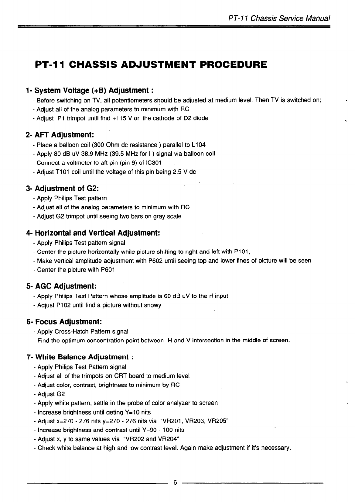
PT-11 CHASSIS ADJUSTMENT
PROCEDURE
l- System Voltage (+B) Adjustment :
- Before switching on TV, all potentiometers should be adjusted at medium level. Then TV is switched on;
- Adjust all of the analog parameters to minimum with RC
- Adjust Pl trimpot until find +115 V on the cathode of D2 diode
2- AFT Adjustment:
- Place a balloon coil (300 Ohm dc resistance ) parallel to L104
- Apply 80 dB UV 38.9 MHz (39.5 MHz for I ) signal via balloon coil
- Connect a voltmeter to aft pin (pin 9) of IC301
- Adjust TlOl coil until the voltage of this pin being 2.5 V dc
3- Adjustment of G2:
- Apply Philips Test pattern
- Adjust all of the analog parameters to minimum with RC
- Adjust G2 trimpot until seeing two bars on gray scale
4- Horizontal and Vertical Adjustment:
- Apply Philips Test pattern signal
- Center the picture horizontally while picture shifting to right and left with Pl 01,
- Make vertical amplitude adjustment with P602 until seeing top and lower lines of picture will be seen
- Center the picture with P601
5- AGC Adjustment:
- Apply Philips Test Pattern whose amplitude is 60 dB UV to the rf input
- Adjust P102 until find a picture without snowy
6- Focus Adjustment:
- Apply Cross-Hatch Pattern signal
- Find the optimum concentration point between H and V intersection in the middle of screen.
7- White Balance Adjustment :
- Apply Philips Test Pattern signal
- Adjust all of the trimpots on CRT board to medium level
- Adjust color, contrast, brightness to minimum by RC
- Adjust G2
- Apply white pattern, settle in the probe of color analyzer to screen
- Increase brightness until geting Y=lO nits
- Adjust x=270 - 276 nits y=270 - 276 nits via “VR201, VR203, VR205”
- Increase brightness and contrast until Y=90 - 100 nits
- Adjust x, y to same values via “VR202 and VR204”
- Check white balance at high and low contrast level. Again make adjustment if it’s necessary.
6
Page 3
PT-11 Chassis Service Manual
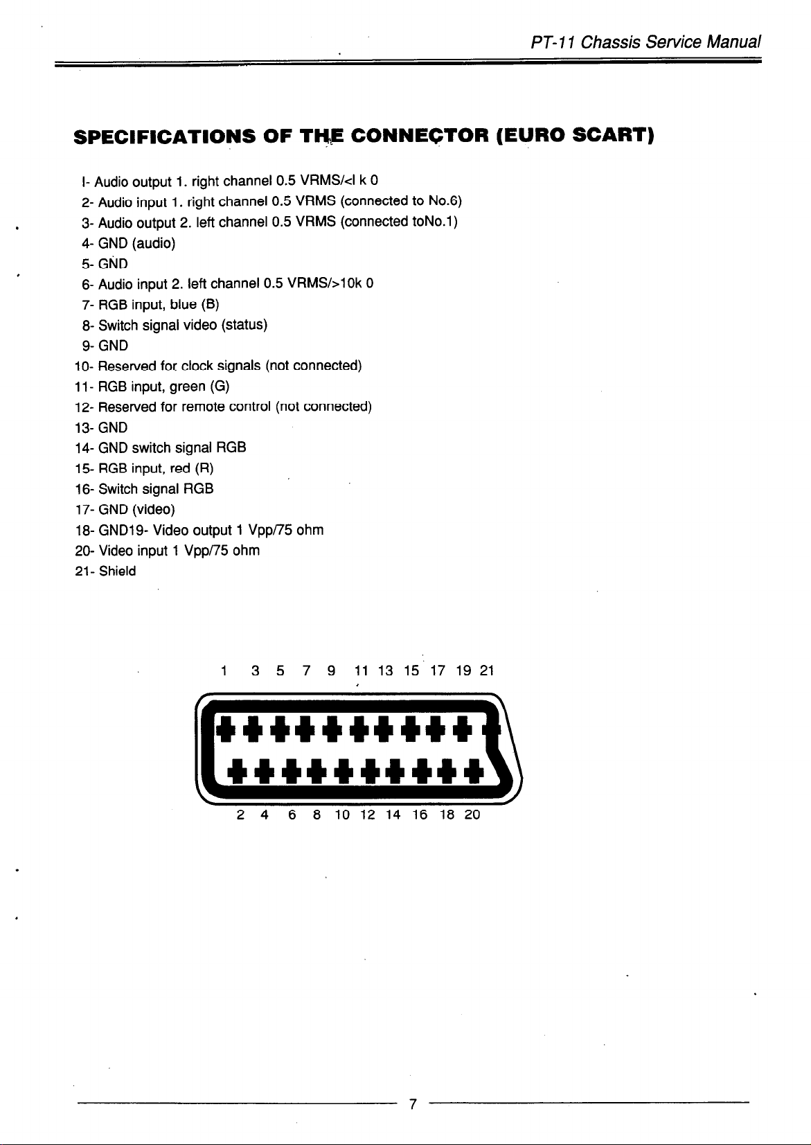
SPEClFlCATlONS OF Tk&E CONNEGTOR (EURO SCART)
I- Audio output 1. right channel 0.5 VRMS/cI k 0
2- Audio input 1. right channel 0.5 VRMS (connected to No.6)
3- Audio output 2. left channel 0.5 VRMS (connected toNo.1)
4- GND (audio)
5- GtiD
6- Audio input 2. left channel 0.5 VRMS/>lOk 0
7- RGB input, blue (B)
8- Switch signal video (status)
9- GND
lo- Reserved for clock signals (not connected)
1 l- RGB input, green (G)
12- Reserved for remote control (not connected)
13- GND
14- GND switch signal RGB
15- RGB input, red (R)
16- Switch signal RGB
17- GND (video)
18- GNDlS- Video output 1 Vpp/75 ohm
20- Video input 1 Vpp/75 ohm
21- Shield
2 4 6 8 10 12 14 16 18 20
Page 4
PT-7 1 Chassis Service Manual
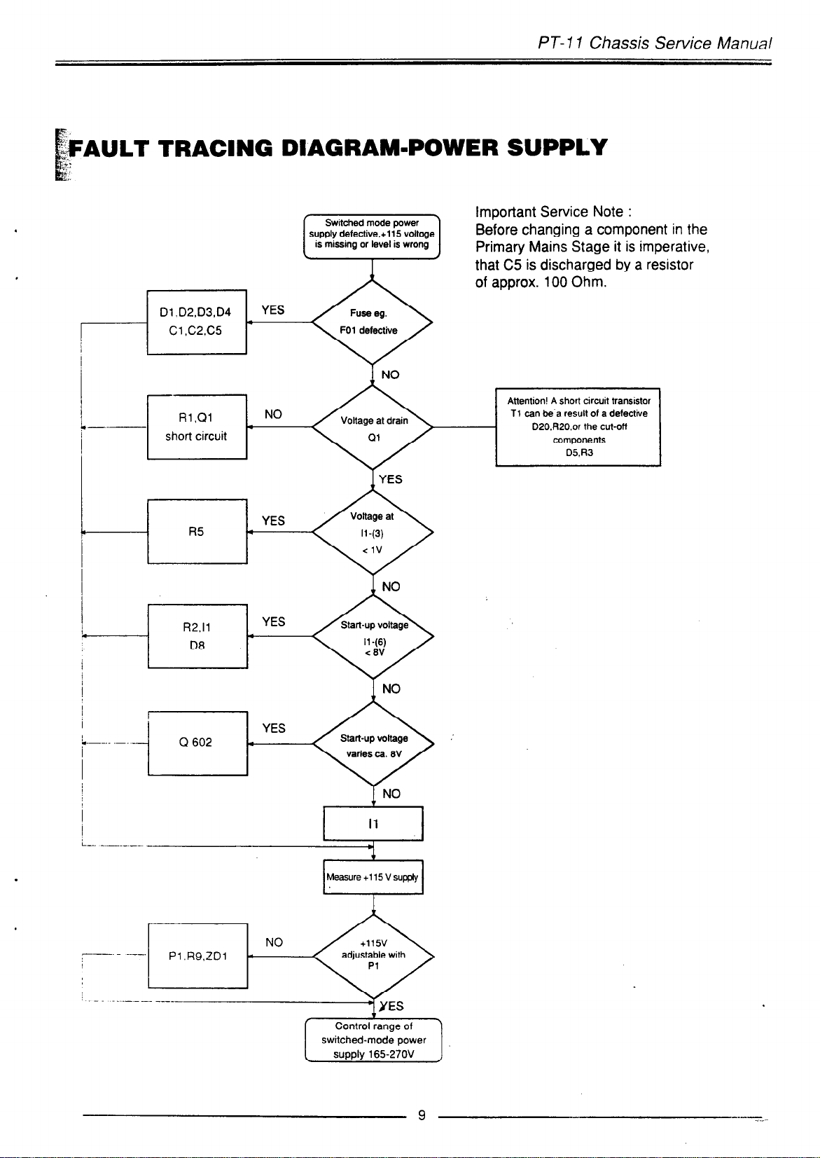
AULT TRACBNG DIAGRAM-POWER SUPPLY
important Service Note :
Before changing a component in the
Primary Mains Stage it is imperative,
that C5 is discharged by a resistor
Attention! A short circuit transistor
Rl .Ql
l-
r-1 short circuit
NO
I
*
I
I
/
I
i._-.. ._. _
I
1 YES
R2.11
D8
Q 602
4
Measure +115 V supply
I
___ ..--
I
Pl .RS,ZDl .
supply 165-270V
Page 5
PT-11 Chassis Service Manual
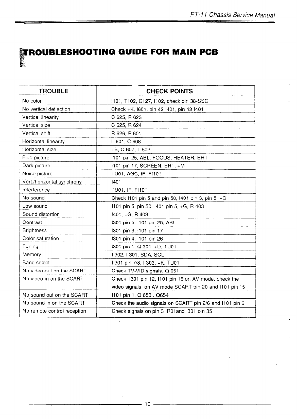
ROUBLESHOOTlNG GUIDE FOR MAIN PCB
I
- -._
TROUBLE CHECK POINTS
No color
No vertical deflection
Vertical linearity
Vertical size
1 Vertical shift
1 Horizontal linearity
/ Horizontal size
/ Flue picture
/picture
1 Noise picture
_--
Vert./horizontal synchrony
Interference
No sound
Low sound
( Sound distortion
Contrast
Brightness
’
Color saturation
Tuning
Memory
Band select
! No video-out on the SCART
No video-in on the SCART
No sound out on the SCART
1 No sound in on the SCART
No remote control reception Check signals on pin 3 IROland 1301 pin 35
I
I
I
1101, T102, C127, 1102, check pin 38SSC
Check +K, 1601, pin 42 1401, pin 43
C 625, R 623
C 625, R 624
R 626. P 601
L601, C608
+B, C 607, L 602
1101 pin 25, ABL, FOCUS, HEATER, EHT
1101 pin 17. SCREEN. EHT. +M
TUOl, AGC, IF, Fll 01
1401
TUOl. IF. FllOl
Check 1101 pin 5 and pin 50, 1401
1101 pin 5, pin 50. 1401 pin 5. +G,
1401, +G, R 403
1301 pin 5, 1101 pin 25, ABL
1301 pin 3, 1101 pin 17
1301 pin 4, 1101 pin 26
1301 pin 1, Q 301, +D, TUOl
I 302, I 301, SDA, SCL
I 301 pin 7/8. I 303, +K, TUOl
Check TV-VID signals, Q 651
Check 1301 pin 12, 1101 pin 16 on AV mode, check the
video signals on AV mode SCART pin 20 and 1101 pin 15
I1 01 pin 1, Q 653 . Q654
Check the audio signals on SCART pin 2/6 and 1101 pin 6
1401
pin 3, pin 5, +G
R 403
/
i
I
I
1
10
Page 6
in
a
PT-11 Chassis Service Manual
0
\t
-
4
-I-
-*-
---
I
/
I
-- .-_
-c
-.-•,
-----D
l
T---y7
,’
!_.
f
0
c-2
0
a
a
n
r
-.- -.
.l.,f- CT
W
>
E
n
e
c
P
3
y-------
------.-_.__J
L
.
Page 7
PT- I 1 Chassis Service Manual
DESCRiPTONS OF THE PARTS
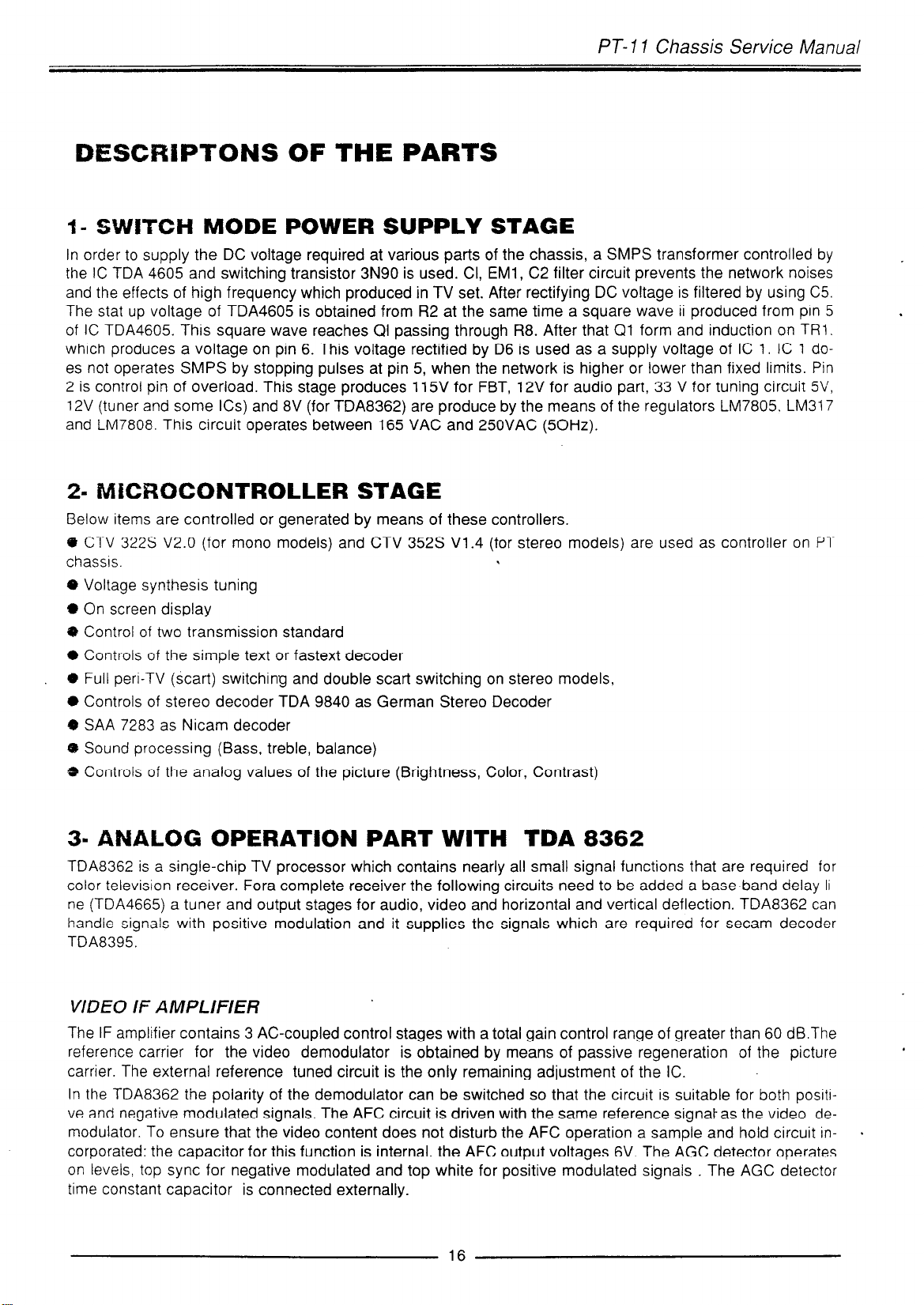
I- SWITCH MODE POWER SUPPLY STAGE
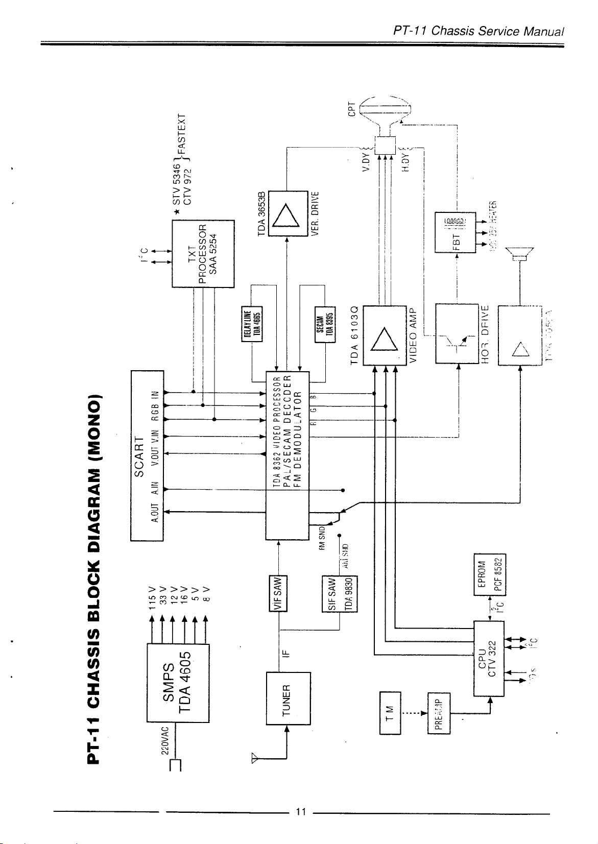
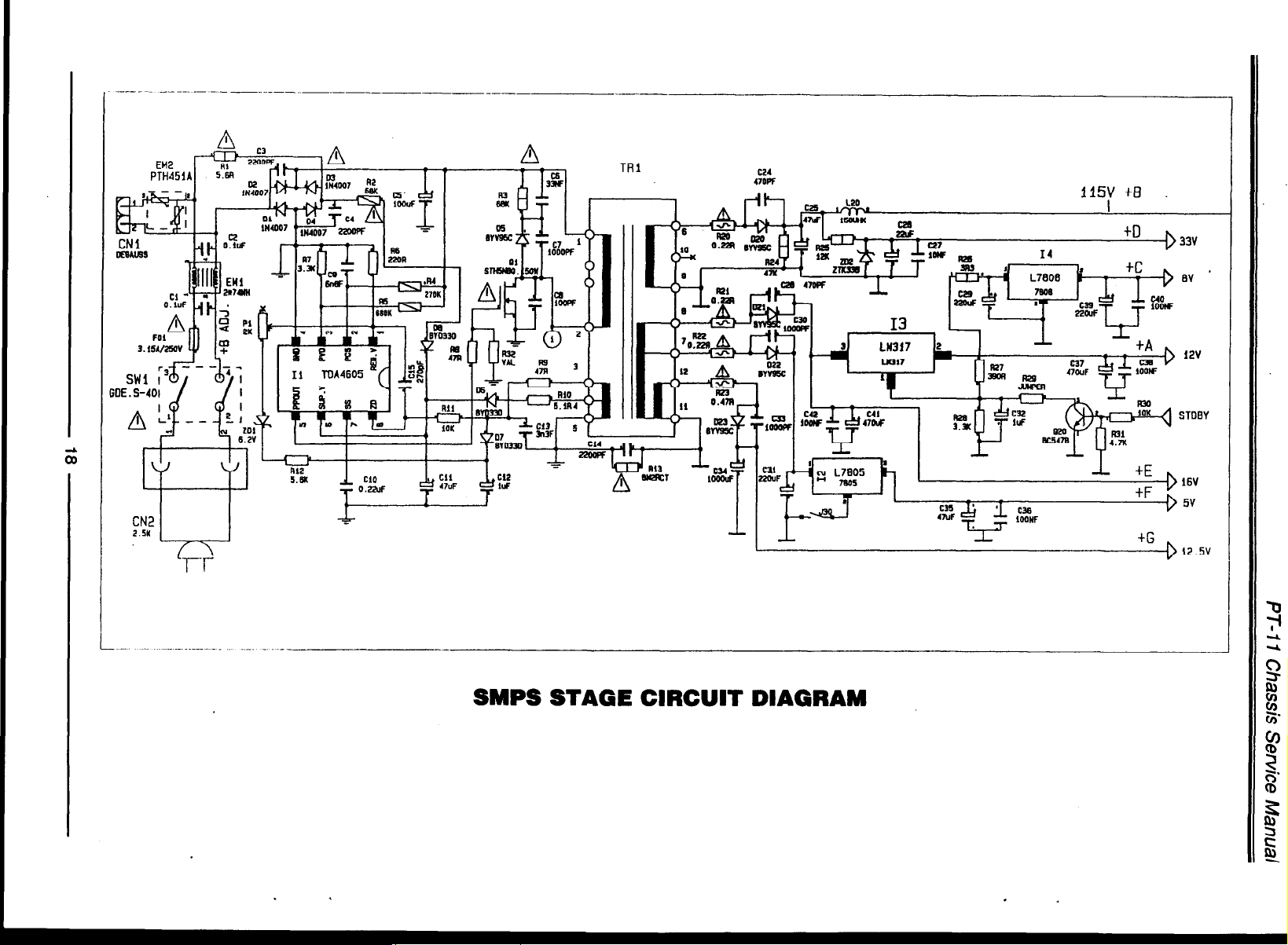
In order to supply the DC voltage required at various parts of the chassis, a SMPS transformer controlled by
the IC TDA 4605 and switching transistor 3N90 is used. Cl, EMl, C2 filter circuit prevents the network noises
and the effects of high frequency which produced in TV set. After rectifying DC voltage is filtered by using C5.
The stat up voltage of TDA4605 is obtained from R2 at the same time a square wave ii produced from pin 5
of IC TDA4605. This square wave reaches QI passing through R8. After that Ql form and induction on TRl.
which produces a voltage on pin 6. This voltage rectified by D6 is used as a supply voltage of IC 1. IC 1 does not operates SMPS by stopping pulses at pin 5, when the network is higher or lower than fixed limits. Pin
2 is control pin of overload. This stage produces 115V for FBT, 12V for audio part, 33 V for tuning circuit W,
12V (tuner and some ICs) and 8V (for TDA8362) are produce by the means of the regulators LM7805. LM317
and LM7808. This circuit operates between 165 VAC and 250VAC (50Hz).
29 MiCROCONTROLLER STAGE
Below items are controlled or generated by means of these controllers.
fo CTV 32.25 V2.0 (for mono models) and CTV 352s V1.4 (for stereo models) are used as controller on PT
chassis.
0 Voltage synthesis tuning
+ On screen display
3 Control of two transmission standard
0 Controls of the simple text or fastext decoder
+ Full peri-TV (&art) switching and double scat-t switching on stereo models,
0 Controls of stereo decoder TDA 9840 as German Stereo Decoder
9 SAA 7283 as Nicam decoder
Q Sound processing (Bass, treble, balance)
a Controls of the analog values of the picture (Brightness, Color, Contrast)
.
3- ANALOG OPERATION PART WITH TDA 8362
TDA8362 is a single-chip TV processor which contains nearly all small signal functions that are required for
color television receiver. Fora complete receiver the following circuits need to be added a base-band delay Ii-
ne (TDA4665) a tuner and output stages for audio, video and horizontal and vertical deflection. TDA8362 can
handle signals with positive modulation and it supplies the signals which are required for secam decoder
TDA8395.
VlDEO IF AMPLIFIER
The IF amplifier contains 3 AC-coupled control stages with a total gain control range of greater than 60 dB.The
reference carrier for the video demodulator is obtained by means of passive regeneration of the picture
carrier. The external reference tuned circuit is the only remaining adjustment of the IC.
In the TDA8362 the polarity of the demodulator can be switched so that the circuit is suitable for both positi-
ve and negative modulated signals. The AFC circuit is driven with the same reference signat as the video de-
modulator. To ensure that the video content does not disturb the AFC operation a sample and hold circuit incorporated: the capacitor for this function is internal. the AFC output voltages 6V. The AGC detector operates
on levels, top sync for negative modulated and top white for positive modulated signals . The AGC detector
time constant capacitor is connected externally.
-
Page 8
PT-11 Chassis Service Manual
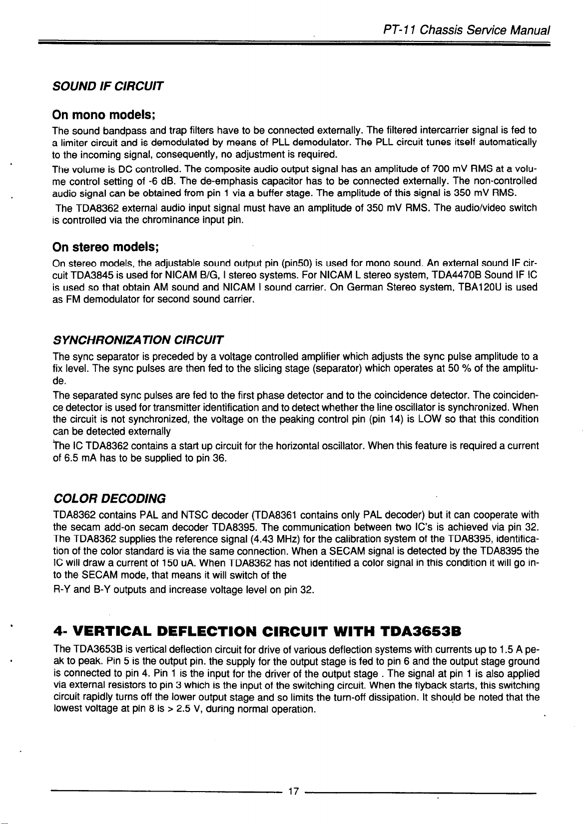
SOUND IF CIRCUIT
On mono models;
The sound bandpass and trap filters have to be connected externally. The filtered intercarrier signal is fed to
a limiter circuit and is demodulated by means of PLL demodulator. The PLL circuit tunes itself automatically
to the incoming signal, consequently, no adjustment is required.
The volume is DC controlled. The composite audio output signal has an amplitude of 700 mV RMS at a volume control setting of -6 dB. The de-emphasis capacitor has to be connected externally. The non-controlled
audio signal can be obtained from pin 1 via a buffer stage. The amplitude of this signal is 350 mV RMS.
The TDA8362 external audio input signal must have an amplitude of 350 mV RMS. The audio/video switch
is controlled via the chrominance input pin.
On stereo models;
On stereo models, the adjustable sound output pin (pin50) is used for mono sound. An external sound IF circuit TDA3845 is used for NICAM B/G, I stereo systems. For NICAM L stereo system, TDA4470B Sound IF IC
is used so that obtain AM sound and NICAM I sound carrier. On German Stereo system, TBA120U is used
as FM demodulator for second sound carrier.
SYNCHRONIZATION CIRCUIT
The sync separator is preceded by a voltage controlled amplifier which adjusts the sync pulse amplitude to a
fix level. The sync pulses are then fed to the slicing stage (separator) which operates at 50 % of the amplitu-
de.
The separated sync pulses are fed to the first phase detector and to the coincidence detector. The coinciden-
ce detector is used for transmitter identification and to detect whether the line oscillator is synchronized. When
the circuit is not synchronized, the voltage on the peaking control pin (pin 14) is LOW so that this condition
can be detected externally
The IC TDA8362 contains a start up circuit for the horizontal oscillator. When this feature is required a current
of 6.5 mA has to be supplied to pin 36.
COLOR DECODING
TDA8362 contains PAL and NTSC decoder (TDA8361 contains only PAL decoder) but it can cooperate with
the secam add-on secam decoder TDA8395. The communication between two IC’s is achieved via pin 32.
The TDA8362 supplies the reference signal (4.43 MHz) for the calibration system of the TDA8395, identification of the color standard is via the same connection. When a SECAM signal is detected by the TDA8395 the
IC will draw a current of 150 uA. When TDA8362 has not identified a color signal in this condition it will go in-
to the SECAM mode, that means it will switch of the
R-Y and B-Y outputs and increase voltage level on pin 32.
41 VERTICAL DEFLECTION CIRCUIT WITH TDA3653B
The TDA3653B is vertical deflection circuit for drive of various deflection systems with currents up to 1.5 A pe-
ak to peak. Pin 5 is the output pin. the supply for the output stage is fed to pin 6 and the output stage ground
is connected to pin 4. Pin 1 is the input for the driver of the output stage . The signal at pin 1 is also applied
via external resistors to pin 3 which is the input of the switching circuit. When the flyback starts, this switching
circuit rapidly turns off the lower output stage and so limits the turn-off dissipation. It should be noted that the
lowest voltage at pin 8 is > 2.5 V, during normal operation.
17
Page 9
I “4 I I ‘“-
1
J p 5v
.-
tG
12.5v
-
SMPS STAGE ClRCUlT DIAGRAM
.
Page 10
PT-11 Chassis Service Mawa/
5- HORfZ6NTAL DRIVE CIRCUIT
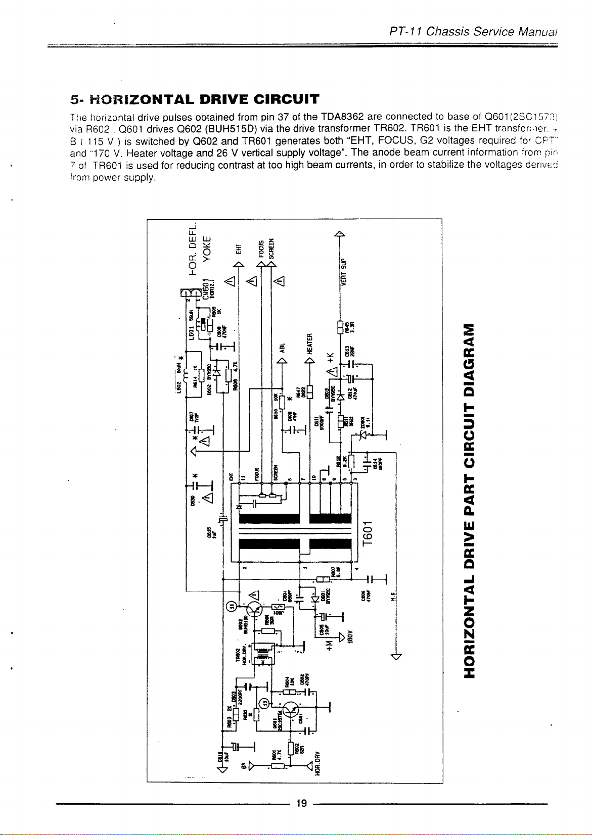
Tl~e horizontal drive pulses obtained from pin 37 of the TDA8362 are connected to base of Q601(2SC: 57i;1
via R602 Q601 drives Q602 (BUH515D) via the drive transformer TR602. TR601 is the EHT transfon>er. r
B i 115 V ) is switched by Q602 and TR601 generates both “EHT, FOCUS, G2 voltages required for CPT”
and “170 V. Heater voltage and 26 V vertical supply voltage”. The anode beam current information from per’
7 of TR601 is used for reducing contrast at too high beam currents, in order to stabilize the voltages dew&
from power supply.
Page 11
PT-1 I Chassis Service Manual
61 SOUND OUTPUT STAGE
.On mono models, TDA7056A is used as sound output amplifier with DC volume control. Pin 50 of the
TDA8362 is AC coupled to the input pin 3 of the TDA7056A via a RC filter. It is supplied by + 12V coming
from a separate winding in the SMPS transformer.
On stereo models, TDA7057AQ is used as sound amplifier. The sound level is controlled by sound processor TDA8425 via 1% bus on stereo boards. The outputs of TDA8425 ( pin 9 and pin 13 ) is connected to
TDA7057AQ via a divider circuit and two capacitors.
71 TELETEXT STAGE
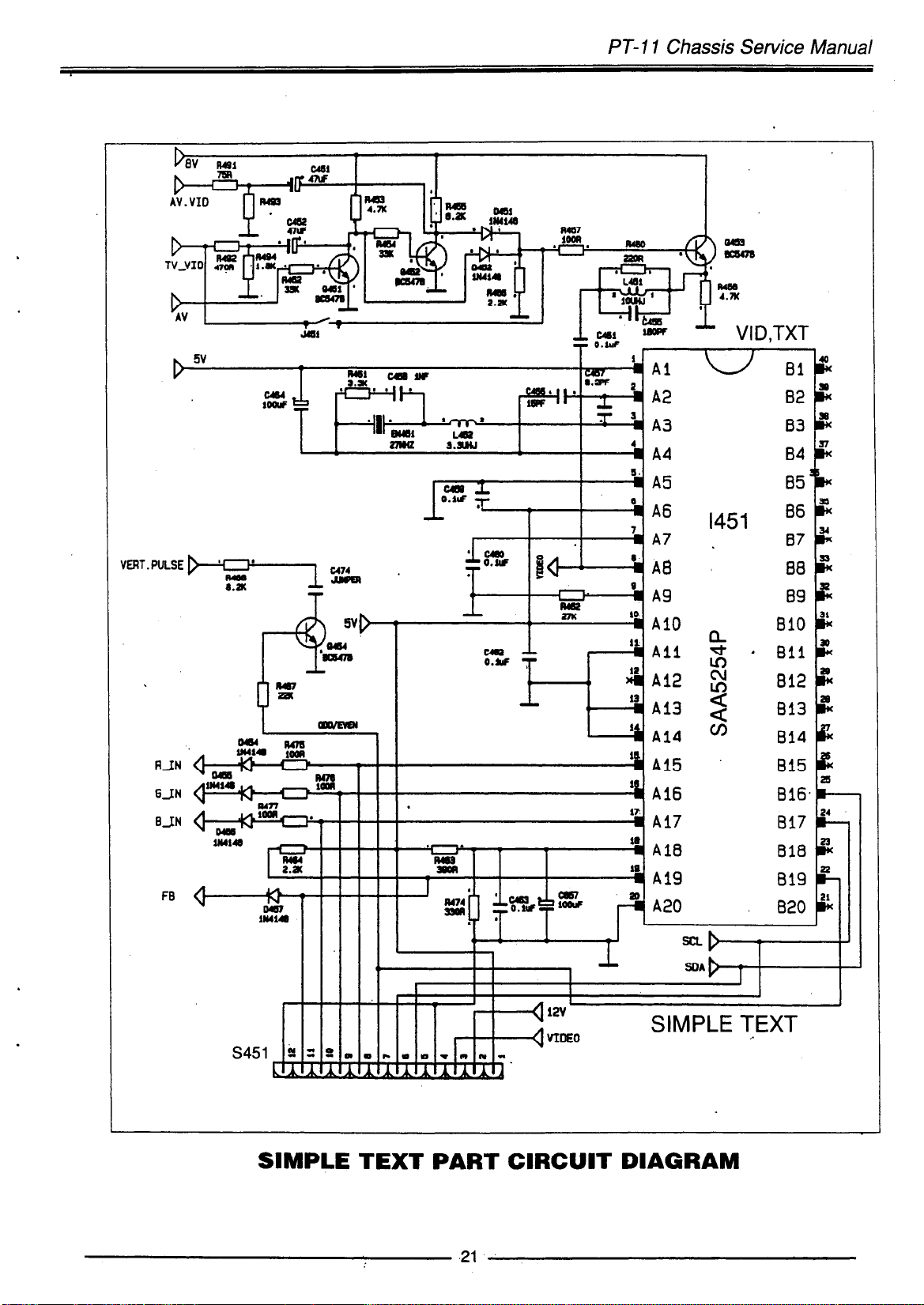
The teletext stage consists of I SAA5254. On this stage, it should be paid attention that there is video signal
on pin 8 of I SAA5254 after a RCL filter, on condition that existence of the other requirements such as +5V,
periferical components.
Basically, fastext stage consists two l’s, STV5346 Teletext decoder and CTV 974 fastext controller with 1%
bus interface. For List Mode a 2K EEPROM (PCF8582) can be added.
81 CRT STAGE
The TDl6103Q is used on CRT stage as video output amplifier. The TDA6103Q consists of three monolithic
video output amplifiers. Each amplifier can be seen as an operational amplifier with negative feedback. The
advantage of negative feedback is that the amplifier characteristics do not play an important role up to certain frequencies.
The device needs only one power supply voltage (+M ). In contrast to previous types of DMOS video amplifiers, the TDA 6103Q does not need a second supply voltage (12V.), so it saves one wire from motherboard
to CRT stage.
As the TDA 8362 has no white point adjustment and no black current set-up, two adjustments are required
for gain and three adjustments for black setting.
Page 12
PT-11 Chassis Service Manual
VERT. PULSE
SlMPLE TEXT PART ClRClJlT DIAGRAM
Page 13

HE DETAILS OF THE BOARDS
Mother Board Contains
PT- 11 Chassis Service Manual
TDA 8362
CTV 322 I
TDA 4605
TDA 4665
TDA 8395
TDA 7056A Audio Output Amplifier (for mono)
TDA 7057AQ Audio Output Amplifier (for stereo)
PCF 8582 2K EEPROM
TDA 3653B Vertical Driver
SAA 5254 Simple Text Processor
TDA 9830 AM Demodulator
LM 317 Voltage Regulator
i_M 7805 Voltage Regulator
LM 7808 Voltage Regulator
Tuner
Infrared Receiver
Horizontal Deflection Part
Degaussing Circuit
4 push buttons ( p+, p-, v+, v-)
Stand By Led
Main Switch
Start Jack
Extension Connectors
multistandard TV processor
CTV 352 S micro controller with OSD
Switch Mode Power Supply Controller
Baseband Delay Line
Secam Decoder
CRT Board
w TDA 6103Q Video Output Amplifier
Page 14

‘x-
________
.
________
________
PT- 11 Chassis Service Manual
t I
a
;ii
24
Page 15

____... _~
PT-I 1 Chassis Service Manual
--.-
Page 16

PT-11 Chassis Service Manual
HE
Video Processing
Video and time base is based on the TDA 8362 Multistandard TV Processor( Pal Decoder),TDA 4665 Baseband Delay Line and TDA8395 Secam Decoder.
The Features of this Concept:
0 Multistandard vision IF circuit (positive and negative modulation)
0 Multistandard FM sound demodulator (4.5 MHz to 6.5 MHz)
0 External Video and Audio Switches
0 Integrated chrominance traps and baseband filters
0 Integrated luminance delay line
0 RGB control circuit with linear RGB inputs
0 Horizontal synchronization with two loops and alignment-free horizontal oscillator without external
components.
0 Vertical count-down circuit (50-60 Hz) and vertical preamplifier
0 Low dissipation
0 Only one adjustment (vision IF demodulator )
DESCRIPTION OF THE
Unit With TDA8362
INTEGRATED CIRCUITS
Block Diagram
36
Page 17

PT-11 Chassis Service Manual
TDA 4665
The TDA4665 is an integrated baseband delay line circuit. It provides a delay of 64 us for the color difference signals. (R-Y) and (B-Y), in multi-standard TVs.
colour-difference
input signals
sandcastle
pulse input
16
SIGNAL
--+ CLAMPING -’
14
SIGNAL _,
- CLAMPING
9
-* analog supply
10
I I I I
GNDl
LINE
MEMORY
‘I
digital supply
“PP
SAMPLE-
-_, ANDHOLD
I-
1-
I
addition
GND2
output
buffers
.3 4,6
Block dianram
- *(R-Y)
colourdlfference
output signals
- *(G-V
- n.c.
2
- n.c.
_ n.c.
- n.c.
- i.c.
39
Page 18

PT- 7 1 Chassis Service Manual
Microcontroller Unit
CTV 352 S(for stereo) and CTV 322(for mono) are a voltage synthesis tuning system with on screen display
OSD of all relevant control function. Analog picture settings are controlled by 4 on-chip digital to analog con-
verters. Sound volume can be controlled by the fifth on-chip digital to analog converter in mono only system.
Full sound ( volume, bass, treble, balance ) in German Stereo and Nicam configuration and Teletext can be
controlled via the l2C bus using a sound processor and teletext decoder. This controllers can control up to two
start plugs.
I
PINNING
1 Tuning voltage control output
2 Volume control output
3 Brightness control output
4 Color control outout
5 Contrast or hue control output
6 Tone, balance or hue control output
7 Band-switch O-output
8 Band-switch l-output
9 Analogue AFC sense input
10 Dual/Non Dual language sound input
11 VTR time constant control output
12 Ext./int. audio/video source control output
13 Keyboard scan line input/output
14 Keyboard scan line input/output
15 Keyboard scan line input/output
16 Keyboard scan line input/output
17 Keyboard scan fine input/output
18 Keyboard scan line input/output
19 Keyboard scan line input/output
20 System mode’strobe output
21 Ground supply input
22 OSD red output
23 OSD areen output
PIN VOLTAGE
: 5v - ov
: 0 - 5v
: -
. _
. _
: 2-4V
: -
i 5, (TV) - OV (AV)
. _
. _
: -
. _
. _
:-
- _
: 5v
:-
: 4.5vpp
: 4.5Vpp
Page 19

PT- I1 Chassis Service Manual
INTN/TO
Tl
:----- -
_:-qy) B ~ i oNs::$E;;:;‘
t-
I
I ,
I
I
RESETNt
TEST-
I
------- -----I
T
I I
8 5
PO Pi
I
I
T T
T T Illli
p 16
DPO LIP1 PWM 1 5
$
J
vow1 vow3
VOB hVOW2 h DOSCl %YNCN
T
TDAC
Block diagram of PCA84C641
Tl INTN/TO
vow1 vow3
T voy T DO~CI TUSY,NCN(
DOSCZ HSYNCN
$6.BIT INTERNAL BUS
T
J
‘2C
T T
AFC SDA SCL
DOSCZ HSYNCN
I
XTAL l-
CTAL 2 c
ESETNf
TEST-
._____JL________L___,
: 1 COUNTER 1 1
I I
!-
--- _____------J
L-__
8 5
PO Pl
III1 IIII
btN~HAlUH
T
AFC
I
I 6KxB I I 126X8 I I
T
T T T
6 B
DPO DPl
T T
yl
PWM 1 5 TDAC
Block diagram of PCA84C841
42
I
t
SDA SCL
Page 20

PT-11 Chassis Service Manual
Power Supply With TDA4605
The IC TDA 4605 controls the MOS power transistor and performs all necessary regulation and monitoring
functions in free running flyback converters.
Features
0 Overload protection
0 Burst operation under short circuit conditions
0 Loop error protection
0 Switch-off if line voltage is too low
0 Line voltage compensation of overload point
0 Soft start for quite start up
0 Chip over temperature protection
0 On-chip parasitic transformer oscillation suppression circuit
7
TDA 4605-3
1 PINNING
1 information Input Concerning Secondary Voltage
2 Information lnout Reaardina the Primarv Current
3 ,lnput for Primary Voltage Monitor
4 Ground
) 5 1 output
1 6 1 SUDDIV voltaae lnout
7 Input for Soft-Start and Integrator Circuit
8 Input for the Feedback of the Oscillator
6
2
r
-I- m-r
4-
“FIEF “6min “6A “6E “6mar
PIN VOLTAGE
ST-BY NORM.
0.4v 0.4v
1V 1.2v
2.1v 2v
ov
0.8V 1 8V (1OVpp) ]
12V 1 12.8V 1
l.lV
0.3v 0.4v
ov
1.9v
5
I
l-
L
3
7
43
6
Page 21

Pin Definitions and Functions
PT-I 1 Chassis Service Manual
Pin No.
1
2
3
4
5
Function
Information Input Concerning Secondary Voltage
By comparing the regulating voltage - obtained trom the regulating winding of the transformer with the internal reference voltage, the output impulse width on pin 5 is adjusted to the load of the
secondary side (normal, overload, short-circuit, no load).
Information Input Regarding the Primary Current
The primary current rise in the primary winding is simulated at pin 2 as a voltage rise by means of
external R&element. When a voltage level is reached thats derived from the regulating voltage at
pin 1, the output impulse at pin 5 is terminated. The %-element serves to set the maximum power at the overload point set.
Input for Primary Voltage Monitoring
In the normal operation V3 is moving between the thresholds V3H and V3L (V3H > V3 > V3L)V3 c V3L: SMPS is switched OFF (line voltage too low).
V3 > V3H : Compensation of the overload point regulation (controlled by pin 2)
starts at V3H : V3L = 1.7.
Ground
output
Push-pull output provides &l A for rapid charge and discharge of the gate capacitance of the power MOS-transistor.
6
7
6
Supply Voltage Input
A stable internal reference voltage VREF is derived from the supply voltage also the switching
thresholds V6A, V6E, V6 max and V6 min for the supply voltage detector.
If V6 > V6E then VREF is switched on and swiched off when V6 c V6A - In addition the logic is
only enable for V6 min e V6 e V6 max-
Input for Soft-Start
Start-up will begin with short pulses by connecting a capacitor from pin 7 to ground.
Input for the Oscillation Feedback
After starting oscillation, every zero transition of the feedback voltage (falling edge) through zero
(failing edge) triggers an output pulse at pin 5. The trigger threshold is at + 50 mV typical.
44
Page 22

PT-11 Chassis Service Manual
TELETEXT PART
Simple text stage consists of SAA 5254 Teletext decoder. This I is controlled via 1% bus.
Basically fastext stage consists two l’s, STV 5346 Teletext decoder and CTV 974 Fastext controller with 1%
bus interface. For List Mode a 2K EEPROM (PCF8582) can be added.
SAA 5254
PINNING
1 + 5v supply
2 27 MHz crystal oscillator output
3 27 MHz crvstal oscillator inbut
4 OV crystal oscillator ground
5 OV ground
6 Positive reference voltaae for the ADC.
7 Video black level storage’pin, connected to ground via a 100 nF capacitor
8 Composite video input pin
9 Reference current input pin. connected to around via a 27kohm resistor
I 10 I +5v SUDDIV
11 STTV/FB/FFB polarity selection pin
12 Sync to TV output pin/line flyback input pin. Function controlled by an
internal register bit (scan sync mode)
13 PLL time constant switch/field flyback input pin.
Function controlled by an internal register bit (scan sync mode)
14 OV ground
15 Dot rate character output of the RED color information
16 Dot rate character output of the GREEN color information
17 Dot rate character output of the BLUE color information
18 DC input voltage to define the output high level on the RGB pins
19 Dot rate fast blankina outbut
20 Ground
21 Programmable output to provide contrast reduction of the TV picture formixed
text and picture displays or when viewing newflash/subtitle pages;open drain output
22 25Hz output synchronized with the CVBS input’s field sync pulses to produce
a non-interlaced display by adjustment of the vertical deflection currents
23 Dot rate character output of teletext foreground color information; open
drain output
24 Serial clock input for the I*C-bus. It can still be driven during power-down
of the device
25 Serial data port for the 12C-bus; open drain output. It can still be driven
during power-down of the device
26 to 40 Internally connected.Must be left open-circuit in application
I
I
PIN VOLTAGE
. _
: -
. _
: ov
: ov
: 5v
. _
: 1vpp
. _
: 5v
: -
: -
. _
: ov
: ov
:-
:-
* _
: 5vpp
: 5vpp
:-
I
I
53
Page 23

PT-1 I Chassis Service Manual
BLAN C%i RGBREF RGB ODD/EVEN
; t t I t t
123 I19 121 Ire 115-17 I22
DISPLAY
HAMMING
CHECKER
AND
PACKET 26
SAA5254 ’ PROCESSING ’
ENGINE
:
l rl:
PAGE
MEMORY
DATA
SLICER
AND
CLOCK
REGENERATOR
4
TELETEXT
ACQUISITION
AND
DECODING
l
A .
I%-BUS +
INTERFACE $j
25
--* SDA
- SCL
T
DCVBS
1
VSS
TIMING
CHAIN
REF+
l
s
OSCOUT
OSCIN
CRYSTAL
OSCILLATOR
INPUT
CLAMP
AND SYNC
SEPARATOR
l
+
_
+ w
DISPLAY
CLOCK
PHASE
LOCKED
LOOP
1
-
- VDD
1c
-
- VDD
- Vss
,
OSCGND
BLACK lick- CVBS POL
VCR / FFB Sl-lV / LFB
Block diagram for SIT129 (DIL40) package
54
Page 24

PT-11 Chassis Service Manual
Vertical Deflection Circuit With TDA3653B
The TDA3653B is a vertical deflection output circuit for drive of various deflection systems with current up to
1.5 A peak to peak.
Features
0 Driver
0 Output Stage
0 Thermal Protection
0 Flyback Generator
0 Voltage Stabilizer
0 Guard Circuit
TDA 36538
VOLTAGE
a
h
THERMAL
PROTECTION
DRIVER
Block diagram
62
Page 25

PT-11 Chassis Service Manual
Video Output Amplifier
On CRT Board, TDA 6103Q is used as video output amplifier. The TDA 6103Q includes three video output
amplifier intended to drive the three cathodes of color CRT.
Features
0 High Bandwith : 7.5 Mhz typical
0 High slew rate : 1600 V/us
0 Simple application with a variety of color decoders
0 Only one supply voltage needed
0 Internal protection against positive appearing CRT flashover discharges
0 One non-inverting input with a low minimum input voltage of 1 V
0 Thermal protection
0 Controllable switch-off behavior
TDA 6103Q
PINNING
1 Inverting input 1
2 lnvertina inout 2
3 Inverting input 3
4 Ground, fin
5 Non-inverting input
6 Supply voltage
7 Cathode
6 Cathode
9 Cathode
output 3
output 2
output 1
---- -------------I 3x
Il
I
I 1
“DD
I
“cm “DD 1 “DD
I
MIRROR 2
“DD
I
I
I
PIN VOLTAGE
I
:l .ovpp
:l .ovDD
:l .ovpp
. _
:I .av
:iaov
: sovpp
: sovpp
: sovpp
1 “DO
16
I
I
mverting
input
(3x1
Block diagram (one amplifier shown)
5. _
THERMAL .
non-Inverting
. input
“ip
Page 26

FOR SECAM L/L’
FUR SECAM L/L’
WSPTUNER
VTUNE ’
VOL
BRIG
SAT
CONT
HUE
BNDO
BNDI
AFC
J IO
J 20
21
ST.AV
FE
EXTl
I6
I KEY3
I7
4 KEY4
ia
l KEY5
a KEY6
n MDSTR
GND
.
P.UP
1-a
-b?f.!&.OX6
1
5102 P.DWN +-
wo7 M
IMIU) N
ma
IMME N
cnm1/L
IIUM N
Da0 M
INN& N
MISTR
N ,,
VI
~~
rim
L
L
Page 27

. TDA7057AQ
a
!%
I
L
I I
1402
ST
4 n 6 I6 n 7 -6
I
STDBY
1301
cn
: IDENT
m
0
SDA
EXT2
RMOT
REST
XTAL2
XTAL i
-__
16owi I I I I
b .._ “f”
T-L-l
AGC +
\
(PAL/SE
TEST
0.0SC1
s
k o.osc2
k V.SYN
in
- H.SYN
I
0
_) Cl62
In.
4.7uFa I
16V
h_
< R-J
( 6-J
( B-J
Page 28

Page 29

Page 30

Page 31

Page 32

Page 33

Page 34

Page 35

Page 36

Page 37

Page 38

 Loading...