

Page 1

Page 2
SERVICE MANUAL
Model:
PDP4273M
N
Safety Precaution....................................................................................1~2
Technical Specifications........................................................................3~9
Circuit Diagram
Basic Operations & Circuit Description..........................................31~35
Main IC Information.................................................................................. 36
Panel Information............................................................................... 37~49
Spare Part List....................................................................................50~54
Exploded View..........................................................................................55
If you forget your V-Chip Password......................................................56
Software Upgrade..............................................................................57~60
.................................................................................... 10~30
This manual is th e latest at th e time of printing, and d o es not
include the modification which may be made after th e printing,
by the c ons tan t improvement of product.
Page 3

Safety Precaution
CAUTION
RISK OF E LECTR IC SHO CK
DO NOT O PEN
A
CAUTION: TO REDUCE THE RISK OF
ELECTRIC SHOCK, DO NOT REMOVE COVER
(OR BACK). NO USER-SERVICEABLE PARTS
INSIDE. REFER SERVICING TO QUALIFIED
SERVICE PERSONNEL ONLY.
A
The lightning flash with arrowhead symbol,
within an equilateral triangle, is intended to
alert the user to the presence of uninsulated
“dangerous voltage” within the product’s enclo
sure that may be of sufficient magnitude to
constitute a risk of electric shock to persons.
The exclamation point within an equilateral
triangle is intended to alert the user to the
presence of important operating and
maintenance (servicing) instructions in the
literature accompanying the appliance.
P R E C A U T IO N S D U R IN G
S E R V IC IN G
1. In addition to safety, other parts and
assemblies are specified for conform ance with
such regulations as those applying to spurious
radiation. These must also be replaced only
with specified replacements.
Examples: RF converters, tuner units, antenna
selection switches, RF cables, noise-blocking
capacitors, noise-blocking filters, etc.
2. Use specified internal Wiring. Note especially:
1) Wires covered with PVC tubing
2) Double insulated wires
3) High voltage leads
3. Use specified insulating materials for hazardous
live parts. Note especially:
1) Insulating Tape
2) PVC tubing
3) Spacers (insulating barriers)
4) Insulating sheets for transistors
5) Plastic screws for fixing micro switches
4. When replacing AC prim ary side components
(transformers, power cords, noise blocking
capacitors, etc.), wrap ends o f wires securely
about the terminals before soldering.
5. Make sure that w ires do not contact heat
generating parts (heat sinks, oxide metal film
resistors, fusible resistors, etc.)
6. Check if replaced wires do not contact sharply
edged or pointed parts.
7. Make sure that foreign objects (screws, solder
droplets, etc.) do not remain inside the set.
M A K E Y O U R C O N T R IB U T IO N
T O P R O T E C T T H E
E N V IR O N M E N T
Used batteries with the ISO symbol
\5<9
for recycling as well as small accum ulators
(rechargeable batteries), mini-batteries (cells) and
starter batteries should not be thrown into the
garbage can.
Please leave them at an appropriate depot.
W A R N IN G :
Before servicing this TV receiver, read the
SAFETY INSTRUCTION and PRODUCT
SAFETY NOTICE.
S A F E T Y IN S T R U C T IO N
The service should not be attempted by anyone
unfamiliar with the necessary instructions on this
apparatus. The following are the necessary
instructions to be observed before servicing.
1. An isolation transform er should be connected in
the power line between the receiver and the
AC line when a service is performed on the
primary of the converter transform er of the set.
2. Comply with all caution and safety related
provided on the back of the cabinet, inside the
cabinet, on the chassis or picture tube.
3. To avoid a shock hazard, always discharge the
picture tube's anode to the chassis ground
before removing the anode cap.
4. Completely discharge the high potential voltage
of the picture tube before handling. The picture
tube is a vacuum and if broken, the glass will
explode.
1/60
Page 4

5. When replacing a MAIN PCB in the cabinet,
always be certain that all protective are
installed properly such as control knobs,
adjustment covers or shields, barriers, isolation
resistor networks etc.
6. When servicing is required, observe the original
lead dressing. Extra precaution should be given
to assure correct lead dressing in the high
voltage area.
7. Keep wires away from high voltage or high
tempera ture components.
8. Before returning the set to the customer,
always perform an AC leakage current check
on the exposed m etallic parts of the cabinet,
such as antennas, terminals, screwheads, metal
overlay, control shafts, etc., to be sure the set
is safe to operate without danger of electrical
shock. Plug the AC line cord directly to the
AC outlet (do not use a line isolation
transformer during this check). Use an AC
voltmeter having 5K ohm s volt sensitivity or
more in the following manner.
Connect a 1.5K ohm 10 watt resistor paralleled
by a 0.15pF AC type capacitor, between a
good earth ground (water pipe, conductor etc.,)
and the exposed metallic parts, one at a time.
Measure the AC voltage across the combination
of the 1.5K ohm resistor and 0.15 uF
capacitor. R everse the AC plug at the AC
outlet and repeat the AC voltage measurements
for each exposed m etallic part.
The measured voltage must not exceed 0.3V
RMS.
This corresponds to 0.5mA AC. Any value
exceeding this limit constitutes a potential
shock hazard and must be corrected
immediately.
The resistance m easurement should be done
between accessible exposed metal parts and
power cord plug prongs with the power switch
"ON". The resistance should be more than
6M ohms.
AC V O LTM ETER
P R O D U C T S A F E T Y N O T IC E
Many electrical and mechanical parts in this
apparatus have special safety-related
characteristics.
These characteristics are offer passed
unnoticed by visual spection and the protection
afforded by them cannot necessarily be obtained
by using replacem ent components rates for a
higher voltage, wattage, etc.
The replacement parts which have these
special safety characteristics are identified by A
marks on the schematic diagram and on the parts
list.
Before replacing any of these components,
read the parts list in this manual carefully. The
use of substitute replacem ent parts which do not
have the same safety characteristics as specified
in the parts list may create shock, fire, or other
hazards.
9. Must be sure that the ground wire of the AC
inlet is connected with the ground of the
apparatus properly.
Good earth ground
such as the w ater
- pipe, cond u cto r,
etc.
AC Leakage C urren t Check
15 0 0 ohmi, lOw a tt
Place this probe
on each exposed
metallic part
2/60
Page 5

Technical Specifications
1. Standard Test Conditions
All tests shall be performed under the following conditions, unless otherwise specified.
1.1 Ambient light : 150ux (When measuring IB, the ambient luminance
1.2 Viewing distance : 50cm in front of PDP
1.3 Warm up time : 30 minutes
1.4 PDP Panel facing : no restricted
1.5 Measuring Equipment : Minolta CA 100 photometer
1.6 Magnetic field : no restricted
PDP4273M
N
^0.1Cd/m2)
1.7 Control settings : Brightness, Contrast, Tint, Color set at Center(50)
1.8 Power input : 120Vac, 60Hz
1.9 Ambient temperature : 20°C ± 5°C (68°F ± 9°F)
1.10 Display mode : Resolution 1024 (H) x 1024 (V) Pixels
1.11 Other conditions :
1.11.1 With image sticking protection of PDP module, the luminance will descend
by time on a same still screen and rapidly go down in 5 minutes. When
measuring the color tracking and luminance of a same still screen, be sure
to accomplish the measurement in one minute to ensure its accuracy.
1.11.2 Due to the structure of PDP, the extra-high-bright same screen should not
hold over 5 minutes for fear of branding on the panel.
3/60
Page 6

Technical Specifications
ELECTRICAL CHARACTERISTICS
2. Power Input
PDP4273M
N
2.1 Voltage
2.2 Input Current
2.3 Maximum Inrush Current
Test condition
2.4 Frequency
2.5 Power Consumption
Test condition
2.6 Power Factor
2.7 Withstanding voltage
3. Display
3.1 Screen Size
3.2 Aspect Ratio
3.3 Pixel Resolution
3.4 Peak Brightness
3.5 Contrast Ratio (Dark room)
3.6 Viewing Angle
3.7 OSD language
120VAC
3.5A
<30 A (FOR AC 120V ONLY)
Measured when switched off for at least 20 mins
60Hz(±3Hz)
330W Typical
full white display with maximum brightness and
contrast
Meets I EC 1000-3-2
1.5kVac or 2.2kVdc for 1 sec
42” Plasma display
16:9
1024x 1024
1400 cd/m2 (Panel module without filter)
3000:1 (Panel module without filter)
Over 160°
English, Spaish, French
4. Signal
AV & Graphic input
4.1.1 Composite signal : AV
4.1.2 Y , C Signal : S-Video
4.1.3
4.1.4 Graphic Input
4.1.5
4.1.6
4.1.7 I/P frequency
Component signal : YPbPr HDTV compatible
: D-Sub 15 pin detachable cable
HDMI : HDMI
PnP compatibility : DDC 1.0
: fH 31.5kHz to 60kHz% 56.25Hz to 75Hz (640x480
recommended)
4/60
Page 7

Technical Specifications
4.2 Audio input
Audio Input(L/Rx5)
4.3 Audio output
Audio Output (L/Rx1) :
PDP4273M
N
1 for DVI / D-Sub
2 for YPbPr
1 for S-Video
1 for AV
Monitor out(L/R)
SPDIF :
5. Environment
5.1 Operating environment
5.1.1 Temperature : 5° to 33°C
5.1.2 Relative humidity: 20% to 85%(non-condensing)
5.2 Storage and Transport
5.2.1 Temperature : -20°C to 60°C (-4° to 140°F)
5.2.2 Relative humidity: 5% to 95%
6. Panel Characteristics
6.1 Type
6.2 Size
6.3 Aspect ratio
6.4 Viewing angle
6.5 Resolution :
6.6 Weight
6.7 Color
6.8 Contrast :
6.9 Peak brightness
Coaxial x 1 (only for HDMI)
FHP (A3)
42”, 994.8mm(W)x587mm(H)x66mm(D)±1 mm
16:9
Over 160°
1024x 1024
Approx 16kg
1073.7 million colors by combination of 10 bits R,G,B digi
3000:1, Peak White, display rate: 1%, In dark room.
1400cd/m2, Peak White, Max. gradation, display rate: 1%.
al
6.10 Color Coordinate
Test Pattern
liformity : Contrast; Brightness and Color control
at normal setting
: Full white pattern
Average of point A,B,C,D and E +/- 0.01
5/60
Page 8

Technical Specifications
6.11 Color temperature : Contrast and Brightness at Normal;
6.12 Cell Defect Specifications
Subject to Panel supplier specification as appends.
7. Front Panel Control Button
PDP4273M
N
Color temperature set at Middle
x=0.285±0.02
y=0.293±0.02
7.1 SEL. Up / Down Button :
VOL. Left / Right Button :
MENU Button :
SOURCE Button :
7.2 STANDBY Button :
7.3 Main Power Switch :
8. OSD Function
Full on screen display
9. Agency Approvals
Safety UL60950
Emissions FCC class B
Select the up or down item in OSD menu.
Press the key to increase the volume left or right.
When selecting the adjusting item on OSD menu
increase or decrease the data-bar.
Press the key to display or exit the menu.
Press the key to select the input signals source.
Switch on main power, or switch off to enter power
Saving modes.
Turn on or off the unit.
10. Reliability
10.1 MTBF: 20,000 hours (Use moving picture signal at 25°C ambient)
11. Accessories: User Manual x 1, Remote Control x 1, Stand x 1, Power Cord x 1, Battery x2.
6/60
Page 9

Technical Specifications PDP4273M
12. Remote Control
1 Standby(<!>): Press this button to turn off to
standby and turn on from standby.
2 Mute(K): Press this button to quiet the sound
system. Press again to reactivate the
sound system.
3 Number buttons: Use these buttons to enter
the password.
® PIP POS. : Press the button to select different
Image Position in PIP Mode.
© Source: Press this button and use ▲ / ▼
button to select the signal sources. AV, S-Video,
YPbPr 1, YPbPr 2, VGA or HDMI.
© Sleep: Press this button to select the sleep
time, such as "15 Min, 30 Min, 60 Min, 90 Min,
120 Min or off.
7 Swap: Press this button to switch the Main
window or Sub window pictures in PIP and
Split Screen.
® VOL +/- : Press these buttons to increase or
decrease the volume.
® P. Mode : Press the button to select different
picture effect, such as "Normal, Vivid, Hi-Bright,
User or Cinema”.
10 System: Press this button to select the color
system, such as "AUTO or NTSC 3.58”.
11 PIP: Press this button to enter PIP function.
12 Enter : Press to enter or confirm.
◄ / ► : They are used as ◄ / ► buttons in
the OSD Menu screen.
▲ / ▼ : They are used as ▲ / ▼ buttons in
the OSD Menu screen.
12 Exit: Press this button to exit the OSD Menu.
12 Menu: Press this button to pop up the OSD
Menu and press it again to exit the OSD Menu.
12 V-Chip: Press this button to enter the V-Chip
Function. (Only for AV or S-Video)
12 Freeze: Press this button to hold on the screen. Press again to normal.
12 C/C: Press this button to enter the Closed Caption Function. (Only for AV or S-Video)
12 Display: Press the button to display the source information.
12 S. Mode: Press the button to select different sound effect, such as "Normal, News,
Cinema, Concert or User”.
20 P. Size: Press this button, the picture will change according to Full, 4:3 or Panoramic.
(inactive for VGA)
3
4
©
8
12
13
15
16
19
©
0
-1 2
-12
'--12
12
12
20
N
7/60
Page 10
Technical Specifications
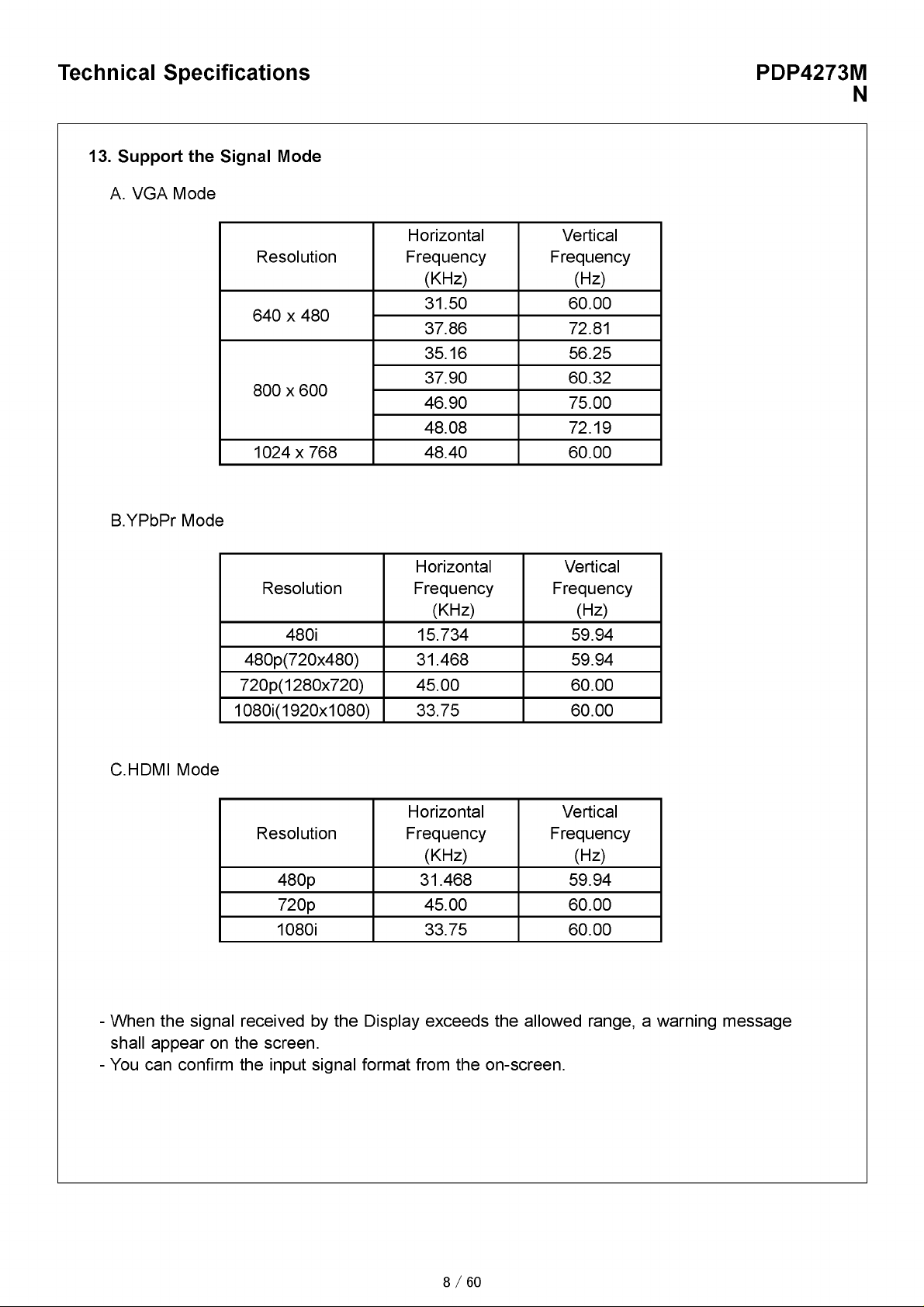
13. Support the Signal Mode
A. VGA Mode
PDP4273M
N
B.YPbPr Mode
Horizontal
Resolution
c ± j\ r\ v A&n
640 X 480
onnv cnn
800 X 600
1024x 768 48.40 60.00
Resolution
480i 15.734 59.94
480p(720x480) 31.468 59.94
720p(1280x720) 45.00 60.00
1080i(1920x1080) 33.75 60.00
Frequency
(KHz)
31.50 60.00
37.86 72.81
35.16 56.25
37.90 60.32
46.90 75.00
48.08 72.19
Horizontal
Frequency
(KHz)
Vertical
Frequency
(Hz)
Vertical
Frequency
(Hz)
C.HDMI Mode
Horizontal
Resolution
480p 31.468 59.94
720p 45.00 60.00
1080i 33.75 60.00
- When the signal received by the Display exceeds the allowed range, a warning message
shall appear on the screen.
- You can confirm the input signal format from the on-screen.
Frequency
(KHz)
Vertical
Frequency
(Hz)
8/60
Page 11

Technical Specifications PDP4273M
N
9/60
Page 12

10/60
ZhonaShan KAWA Electronic Inc
te MT820 2 B l o ck
Page 13
Circuit Diagram
- Main (Video) board
- Keypad board
- Remote control receiver board
- External L/R Speakers board
- Remote control board
Page 14

11/60
Page 15

MT8202E (PBGA388) LCDTV BOARD 4 LAYERS FOR AKAI
1. INDEX / POWER / RESET / EEPROM
2. LDO
3. MT8202E PBGA388
4. MT8202 DECOUPLING
5. DDR MEMORY & FLASH
6. MT5351 INTERFACE
7. HDMI MT8293
8. DAUGHTER BOARD IN
9. WM8776 & VIDEO BYPASS
10. AUDIO / VIDEO IN CIRCUIT
11 . VGA & PC AUDIO IN
12. LVDS OUT
13. BACK LIGHT / KEYPAD
14. TUNER IN
15. AV IN
16. AUDIO IN
17.AUDIO Amplifier
9VV 9V
9VV 9V
FB42^-., FB/NC
LVDSVDD
SCL
SDA
JRST#
3202JP3
GPIO2
GPIO4
9V
»LVDSGND
»SCL
— SDA
»URST#
»8202JP3_
»GPIO2
»GPIO4
— GPIO14
»9 V
—>>VS_ON
HOIF/GND
KAWA Con fiden tial
Z h o n a S h a n K A W A E l e c tr o n ic I n c..
IN D E X / P O W E R / R E SET / E E P R OM
12/60
Page 16

Power ON alive source
5VSB
CB7
I " '
AZ 111 7- 3.3V
U3
N G O U T
SB33
_
____
1+ CE7 = :=
„-p.. 100uF/J"-
ASB33A
ADCV33A
SB33B
ASB33A
SB33A
00uF/16v
LVDS GND
SB33A
U4 AZ1 117 /a dj
IN (S> OUT
> R773_
110 1%
> R774
1“
1 . 2 5 x ( 1 + 6 2 / 1 1 0 ) = 1 . 9 5 V
AS B 18A
_ L . CE9
100uF/16^ ^ CB1(
T
SB18A
J ° 1uF
AZ 111 7- 3.3V
SOT223/SMD
DV33B
AV33A
T
Z
U37 A Z11 17/ad j
IN o OUT
13/60
DACVDD
T
220uF/16v
LVDS GND
' l.
1 . 2 5 x (1 + 1 8 0 /3 0 0 )= 1 .9 9 V
KAWA Con fiden tial
Z h o n g S h a n K A W A E le c tr o n ic I n c .
LDO
Size ¡Document Number Drawn: <Designer> Rev
C AKAI M T820 2 27US L VDS V0 .0 r T T T -------------------
C - - - - Checked:
Page 17

SB333
-)->AUDIO_GND
AADCVSS
»AAÜCVSS
-»LVDS_GND
-»VFE_GND
->>VFE_GND1
AVDD VAD1
->>AVDD_VAD1
PLLVDD1
»PLLVÜÜ-
PLLVDD2
»PLLV0Ü2
PLLVOOl
PLLVÜÜi
XTALVDD
— XTALVDD
VPLLVDD1
»VPLLVÜÜ-
DACVDDA
» üacvüüa
DACVDDB
» üacvüüe
DACVDDC
DACVDDC
AVDD VFE0
->>AVDD_VFE0
AADCVDD DACVDDC DMIVSYNC
» aaücvüc
» aüacvüc DV25A
ADCVDD PWM1
»A0CV0C
— VPLLVDD2
LVDDA AN7
» lvüüa
LVDDB CLK2 SDV25A
»LV00E
LVDDC
»LV00C
OTESTP2
►>TESTP3
»Stestn:
>>TESTP4
>>TESTN4
AVICM CVBS0
>>AVICM
PWM2VREF 0Q23 CVBS1 PWM0
»FWM2VREF
DACFS CLK1 CVBS2 PWM1
>>DACFS
REFP AP2 GND GPI00
ÄREFF
REFN AN2 SY0
»REFN
SB33B
SB33B
PLLVDD1
LVDS GND B22
C21
.VÜS GND A23
dLLVÜÜ3 B21
A20
A21
TP80
4 TP12
aücvüü 27MHZ
PWM2VREF C18
4 TP45 $
4 TP46 A
4
4 TP47 ^
4 TP31®
4
4
4
4
4 TP8 A
TP9 A
4 TP10g
B18
DACVDDA C16
LVDS_GND C17
DACFS
A16
DACVREF OMIHSYNC
B16
VPLLVDD1 015
LVDS GND n14
012
C11
C10
AN6 GND
010 T14
AP5 NT0#
C9
AN5
09
LVDDB DQ24
C13
AP4 DQS3 SCL1
C8
AN4 SDV25A SDA1
08
AP3
A12
AN3 GND
A11 AF13
311
A10
AN1 SC1 GPI04
39
AP0 SDV25A GPI07
AN0 RED GPIOE
K4
07 AF11
SB33A BLUE
05
E202UP3 5 GND VGASOG
C7
VSYNC
36
HSYNC GND
A6
DE
C6 AE1
VCLK
06
0A0 DV25A PR0-
C2
D7 S0Y0
C4
GND
D4
A2
GND
03 SDA0
33
D0 RXD1
A4
OE# TXD
35
OCE#
A5
0A1"
C1
K3
02
01
e4
DO O O c
*3? s'*
PLLVDD-
PLLVSS2
PLLV002
PLLVSS3
PLLV003
XTALV0Ü
XTALO
XTALI
XTALVSS
A0CVSS
A0IN4/GPI0
A0IN3/GPI0
A0IN2/GPI0
ADIN1/GPIO
ADIN0/GPIO
ADCVDD
PWM2VREF
SVM
B
DACVSSA
G
DACVDDA
DACVSSE
DACVDDB
R
0ACVSSC
FS
VREF
DACVDDC
TP4
TN4
VPLLVDD1
VPLLVSS
VPLLVDD2
LVDDA
A7P
A7N
CK2P
CK2N
LVSSA
A6P
A6N
A5P
A5N
LVDDB
A4P
A4N
A3P
A3N
LVSSB
CK1P
CK1N
A2P
A2N
LVDDC
A1P
A0P
A0N
LVSSC
nvnn18A
GPIO
0V0033A
UP3_5
VSYNCO
HSYNCO
GPIO
GPIO
A17
IOA0
AD7
0VSS1E
AD6
A05
AD4
DVSS33
A03
AD2
AD1
AD0
IOOE#
IOCS#
IOA1
nvnn18A
HIGHA7
HIGHA6
HIGHA5
NC BALL
NC BALL
NC BALL
NC BALL
NC BALL
NC BALL
iQQQQoQiQQQQoQQQSa
MT8 202
SO CK E T
go
x 0 0 0 z > 0 0 0 0 >
»SoSoöooSoogoooooooooooo-
> 0 0 0 > 0 0 0 0 > 0 0 0 > 0 0 > > 0 > 0 0 > 0
NC BALL
NC BALL
NC BALL
DVSS
0VSS33I
VCLK_DVI
üvü ü1E
DE_DVI
HSYNC_DVI
VSYNC_DVI
CEN_DVI/GPIO
DE_SOG/GPIO
OUT_27MHZ/GPIO
GPIO/PWM1
GPIO/PWM0
0V0033I
DQ3-
0Q30
0Q2S
DVDD25OPT
0Q2E
DQ27
DVSS25
DQ26
0Q25
DQ24
OQSi
DVDD25OPT
DQM1
0VSS1E
DQS2
0Q23
DQ22
DVSS25
DQ21
DQ20
üvü ü1E
0Q1S
DVDD25OPT
0Q1E
DQ17
DQ16
RA4
RA5
DVSS25
RA6
RA7
RAE
0VSS1E
RAS
RA11
CKE
DVDD25_CLK
RCLK
RCLKB
DVSS25
RA3
RA2
RA1
RAC
RA10
DVDD25
BA1
üvü ü1E
BA0
RCS#
RAS#
DVSS25
CAS#
RWE#
0Q15
DQ14
0Q13
DVDD25
DGND/BALL
DGND/BALL
DGND/BALL
DGND/BALL
ogno/ball
LL LLLL DGND/BALL
ogno/ball
§ § §
3S S ogno/ball
ogno/ball
AF25
A024
AE24
AF24
AD23
AE23
AF23
R15
AD22
VIS
AE22
VIE
AF22
VI7
AC21
VI6
AD21
VI5
AE21
VI4
AF21
VI3
AD20
VI2
AC22
AE20
VI1
AF20
VI0
AC19
AD19
AD18
AC18
AD17
AC17
AC15
AE15
AD14
AF15
AD15
AE14
R14
A01
AC9
AC14
AE12
AE11
R11
AF5
A04
AC6
GND
GND
VI1
VI0
27MHZ SDV25A
PWM0 R
ÜV33AVPLLVDD2
SC0
SY1
VGAHSYNC#
GND
DV25A
GND AOLRCK
DV25A
GND
GND
GND
GND
GND
GND
GND
GND
--
SVCVBS0
«CVBS-
«CVBS2
O.SY0
«SC 0
KSY1
«SC 1
GREEN-
GREEN-
>>VGAS0G
WGAHSYNC#
>>VGAVSYNC#
PB0-
PR0-
S0Y0
S0 Y1
SB33B
CLK1
iÜMiiMi^lk
DV25AADACVDD
OCE#
GPI01
VCLK
RXD
AOMCLK
AOBCLK
ADIN
A0S0ATA1
FCLK
FDAT
>>VI[0..23]
»HÜMIMCLK
►Shümibclk
»Shümilrck
&HÜMISÜ0
&H0MIS01
OHÜMISÜ2
►Shümis üi
»Shümioück
>>hümiüe
» hümihsync
» hümivsync
» hümicen
>>üe_sog
>>27MHZ
A_ÜQS[0..3]
A_RAS#
A_CAS#
A_WE#
SDV25A
<|R
< F_A21
SlOCE#
>>F_OE#
►SlOWR#
►>F_A[8..20]
>>F_Ü[0..7]
>>I0A[0..7]
■' urSt#
INT0#
SÜA_8202
>>SCL_8202
> SCL1
/ S0A1
»AÜCJN0
►>8202UP3_0
>>8202UP3_1
>>FWM0
&F^M 1
OGPI00
►>GPI01
>>GPI02
>>GPI0i
>>GPI04
►>GPI07
►>GPI0E
>>GPI0S
»GPI010
»GPIOr
&GPI012
►»GPI013
>>GPI014
»>GPI015
»>GPI016
&GPI017
»GPI01E
>>GPI01S
>>VCLK
>>CCIR_VCLK
OCCIR_V7
►>CCIR_V6
>>CCIR_V5
>>CCIR_V4
>%CCIR_V[0..3]
►> SCL0
►>SÜA0
>>AÜC_IN4
>>TXÜ1
>>TXC
>RXC
^OMCLK
>A0BCLK
Caolrck
>$aüin
►A0SÜATA1
>>A0S0ATA2
>>AL
>>AR
S MPX
►>MFX2
>>FCLK
>>FCMC
>>FÜAT
0SCL_8202
►>SÜA_8202
SB33A 9
SB33B 9
SB33A
SB33B
SB1EA
-S1
DV33A 9
DV33A
GND
| NC
Z h o n g S h a n K A W A E le c tr o n ic I n c.
MT8202E PBGA388
KAWA Con fiden tial
SB 33 3 S B 333
14/60
Page 18

STAND BY ANALO G POW ER
XTALVDD
— XTALVDD
ADCVDD
»ADCVDC
AVICM
»AVICM
PWM2VREF
»PWM2VREF
DACFS
»DACFS
LVDDA
»LVDDA
LVDDB
»LVDDE
LVDDC
»LVDDC
AADCVDD
»AADCVDC
ADACVDD
»ADACVDC
VPLLVDD1
»VPLLVDD-
VPLLVDD2
»VPLLVDD2
AVDD VAD1
—»AVDD_VFE1
PLLVDD1
»PLLVDD-
PLLVDD2 TESTP3 PLLVDD1
»PLLVDD2
PLLVDD3 DACVDDB
»PLLVDD3
DACVDDA
— DACVDDA
DACVDDB
»DACVDDE
DACVDDC TESTN4 VPLLVDD1
»DACVDDC
TESTP3
TESTN3
TESTP4
TESTN4
REFP
REFN
AADCVSS
AUDIO GND
AADCVSS
TESTP3
TESTN3
TESTP4
TESTN4
REFP
REFN
AADCVSS
AUDIO_GND
LVDS_GND
VFE_GND
AADCVSS
VFE_GND1
ASB18A
T
T_
ASB33A
+ CE26
----
10uF/10V
DS_GND
NORMAL VIDEO DAC POW ER
DACVDD
T
BEAD/SMD/0603
T
T L
BEAD/SMD/0603
T
T L
BEAD/SMD/0603
T
T L
NORMAL VIDEO DAC POW ER
AV33A
_
FB10 -
BEAD/SMD/0603
T
x
T
-X
T
x
T
x
T
x
XTALVDD
ADCVDD
CB29
0.1uF
LVDS_GND
DACVDDA
DACVDDC
NORMAL ANALOG POW ER
ASB18A
AV33A
i C „ C.
„-p. 10uF/10V 1uF
I LVDS GND I
NORMAL VIDE O A DC POWER
ADCV33A
____
FB9 FB
FB11 s-Y-\ FB
T
"L
r
"L
r
"L
REFP
I C49
H ^ 10uF/10v ~*_
REFN
VPLLVDD2 TESTN3 PLLVDD1
T
x
CB36
0.1uF
LVDS GND
AVDD_VFE0
TESTP4 VPLLVDD1
MT8202 DIGITAL POWER & DECOUPLING
I
I C0805/SP
SB33A
X
T
x
1
J
ADCV18A
NORMAL AUDIO ADC / DAC PO WER
ADCV33A
L/IND/DIP/P10.0
r
----
+ CE33
10uF/10V
DCVSS
ADCV33A
+ CE35 I C
10uF/10V 1
AUDIO GND
AVICM
AADCVDD
T
AADCVSS PWM2VREF
x
ADACVDD
CB48
T
0.1uF
AUDIO GND
x
r
L
AUDIO GND
DACFS
=î= C3
D
T
I
T iou
C0
01uF
C060
AADCVSS
LVD:
Z h o n g S h a n K A W A E le c tr o n ic I n c.
MT8202 DECOUPLING
Size Document Number Drawn: <Designei>
C AKAI M T820 2 27US L VDS V0 .0 , ,
15/60
C Checked: <
KAWA Con fiden tial
Page 19

■QSI0--31 w A_DQS[0..3] 3
Z ^ S s A_RA|0--11] 3
A_BA[0--1] 3
E-T O f A_DQM[0--1] 3
A_DQ[0--31] 3
A_CLK
A_RAS#
A_CAS#
A_WE#
IOA|0--7]
DV25A
SDV25A
VREF
IOA|0--7]
F_D|0--7]
IOCE#
F_OE#
IOWR#
F_A[8--20]
DV25A
SDV25A
DQ7 1
7
4
RN17 47x4
A_DQ20 7 8 D_DQ20
_______6_____________________
dq24_ 7 8 D_DQ24
DQ25 5 6 D DQ25
DQ28 7
DQ31 1
RN2i
S “ ! #— 7 8 D-CAS#_
RAS# 1
DV25B
DV25B DV25B
21 8M x 16
66
64
61
58
54
VREF D_RA11 8
49
48
47
44
41
38
37
66
64
61
58
54
VREF
48
44
41
VDD
DQC
VDDQ
DQ1
DQ2
VSSQ
DQ3
DQ4
VDDQ
DQ5
DQ6
12 55
VSSQ
DQ7
NC
15 52
VDDQ
LDQS
NC
18
VDD
DNJ
20
LDM
WE
CAS
RAS
24
CS
NC
BA0
BA-
28
A10/AP
A0
30
A1
A2
A3 DDR
33 34
VDD
HY5DU281622ET-5 8Mx16 TSOP(II)-66/SMD
DV25B DV25B
VDD
DQ0
VDDQ
DQ1
DQ2
VSSQ
DQ3
DQ4
VDDQ
DQ5
11
DQ6
12 55
VSSQ
DQ7
NC
15 52
VDDQ
LDQS
NC
18 49
VDD
D_DQM1 D_DQM1 RN22
DNJ
20 47
LDM
21 46
WE
CAS
RAS
CS
NC
BA0
27 40
BA"
A10/AP
A0
A1
A2
A3 DDR
33 34
VDD
HY5DU281622ET-5 8Mx16 TSOP(II)-66/SMD
D RA7 4
D_DQ0 7
D_DQ3 1
D_DQ4 7
D_DQ8 7
D_DQ11 1
RN15
D DQ12 7
D DQ15 1
D_DQ17 4
RN20
D DQ20 2
D_DQ23 8
D DQ27 1
RN23
D_DQ31 1
D_DQ28 7
RN24
DCS# 7
D DQS2 R70 .
D DQS3 R72 .
D CAS# R75 .
D WE# R77 .
D DQM1 R79 .
D DQS1 R81 .
D_ DQM0 R85 .
D1V25
D1V25
T
- 1_ CB67 CB68
0-1uF 0-1uF
I
t
- CB74 CB75 CB76 CB77 CB78 CB79 CB80 CB8'
0-1uF 0-1uF 0-1uF 0-1uF 0-1uF 0-1uF 0-1uF 0-1uF
T
“ *"" CB82 CB83 CB84 CB85 CB86 CB87 CB88 CB89 CB90 CB91 CB9:
0-1uF 0-1uF 0-1uF 0-1uF 0-1uF 0-1uF 0.1uF 0-1uF 0-1uF 0-1uF 0.1uF
T
-1 _ C40 C41 C42 C43 C44 C45 C46
3300pF 3300pF 3300pF 3300pF 3300pF 3300pF 3300pF
T
D1V25
CE40
220uF/16v
DV25B
TXT
I I
1
i
PUT ON NEARLY BGA
I | | CB116 | CB117 | CB118 | CB119
- 1- C54 ^ C55 ^ ^ ^ ^
3300pF 3300pF 0-1uF 0-1uF 0-1uF 0-1uF
SDV25A DV25B DV25A
T
I
16/60
I CB112 | CB113 CB1
j 0-1uF I 0-1uF
, CE45
‘ 220uF/16v
KAWA Con fiden tial
Z h o n g S h a n K A W A E le c t ro n ic I n c.
DDR MEMORY & FLASH
Size Document Number Drawn: <Designer>
C AKAI M T820 2 27US L VDS V0 .0 , ,
C - - - - Checked: <
Page 20

HM n » VII0--23]
HDMICEN
--------
HDMICEN
HDMIODCK
HDMIHSYNC
HDMIVSYNC
HDMISD1
HDMISD2
HDMISD3
HDMIODCK
HDMIDE
>> HDMIHSYNC
>> HDMIVSYNC
>>DE_SOG
>>INT0#
>>CCIR_V1
>>CCIR_V3
>>SCL_8202
>>SDA_8202
»27MHZ
»HDMIMCLK
»HDMIBCLK
&HDMILRCK
>>HDMISD0
>>HDMISD1
»HDMISD2
&HDMISD3
DV33B DV33B
CE609
_L l _ Ci
"T ' 10uF/16^ 0 1u
CE613
_L+ _ _ Ci
*”^ 10uF/16v 1 0 1u
CE614
_L+ _ _ Ci
*”^ 10uF/16v ' 0 1 u
HDMI_PLUGPWR
CE610
100uF/16v
VCC
AVCC
^ CE
^ 0
AVCC
OVCC
PVCC
REGVCC
U48 A Z1117 -1 .8
DN
3
+ CE611 + CE612
^ CB21
0-1uF
47uF/16v
C :c
V J» NC
— NC
EEPROM 24C04/CODE
NC WP
NC SCL
GND SDA
SOT223/SMD 47uF/16v
DV33B DV33B DV33B
C VCC
KWP
NC VCC
NC WP
NC SCL
GND SDA
EEPROM 24C04/CODE
DV33B
*
HDMI_PLUGPWR
R69i
SDA 8202 R698
9993~SDA R700
9993 SCL R701
CI2CA
PLJGPWR
PVCC
AVCC
CLOCK
CLOCK
AVCC
AVCC
AVCC
DATA2 AVCC IOVCC
DATA2 OVCC
HDMIRST#
XIL XILC DATA1
27MHZ
I CB219 C617 I CB220 | C618 | CB221 | C619 | CB222 | Cf
^oooaooooc
G1
ePad/GND
GPIO2
GPIC
GPIOC
CVCC18
CGND18
CI2CA
CSDA
CSCL
DSDA
DSCL
CEC
PWR5V
CVCC18
PGND
PVCC
EXT_RES
AVCC
50
RXC-
51
RXC+
52
AGND
53
AVCC
RX0-
RX0+
AGND
AVCC
RX1-
RX1 +
AGND
AVCC
RX2-
MT8293
CB234 | Ci
, ^ ,
128
HSYNC
DE
CGND18
CVCC18
QE0
QE1
QE2
QE3
IOVCC33
ODCK
IOGND33
QE4
QE5
QE
6
QE7
CGND18
CVCC18
QE8
110 6 5
QE9
QE10
QE11
IOVCC33
OGND33
QE14
QE15
IOVCC33
OGND33AGND
DV33B
VCC18
OVCC
VCC18
OVCC
LQFP128/SMD/8293
INT0#
R709 47k
8 7
RN28 33x4
8 7
-----2 V / v
RN29 33x4
4
-----2
RN30 33x4
6 5
4
SB33B
^ 1uF ^ 1000PF 1000PF 1000PF _■
I CB224 | C622 | CB225 | C623 | C621 | CB22
1000PF 1000PF 1000PF 0 1u>
OVCC
I CB226 I C624 | CB227 | C625 I CB228 I C626 I CB229 I C
^¡= ^ ¡ = ^ ¡= ^ ¡= ^ ¡ = = |= 1000PF= ;= = ;=
| 0- 1uF I 1000PF 0- 1uF I 1000PF 0- 1uF | 0- 1uF | 1
I CB230 | C628 | CB231 | C629 | CB232 | C630 | CB233 | C
| 0- 1uF | 1000PF | 0- 1uF | 1000PF | 0- 1uF | | 0- 1uF | 1
I C614 | CB215 | C615 | CB216 |
^ 1000PF 1000PF _■
________
________
,
C627
000PF
C631
000PF
C616
000PF
,
CI2CA
R696
4 - 7K/NC
17/60
KAWA Con fiden tial
Z h o n g S h a n K A W A E le c t ro n ic I n c.
HDMI INPUT MT8293
Size IDocument Number Drawn: <Designei> Rev
C AKAI M T820 2 27US L VDS V0 .0 r = = = -------------------
C Checked:
Page 21

18/60
Page 22

Page 23

Page 24

Page 25

GREEN
BLUE
BLUE
VGASOG
VGAHSYNC#
VGAVSYNC#
TXD
RXD
RED+
RED- 3
GREEN+ 3
GREEN- 3
BLUE+ 3
BLUE- 3
VGASOG 3
VGAHSYNC# 3
VGAVSYNC# 3
TXD
RXD
VGAR_IN 9
VGAL_IN 9
■ VFE_GND 2,3,
VGA IN
VCC
NEARLY VGA CON
NEARLY 8202
DIODE SMD BAV99
DIODE SMD BAV99
VGA PLUGPWR
EEPROM 24C02
VGA_PLUGPWR
VGASCL
VGASDA
RCA1X2 AV2-8-4-13P
^ 1
_________
^ 2
________
cha nge
VGAR IN
VGAL IN
22/60
VGA/DVI AUDIO INPUT
Z h o n a S h a n K A W A E le c tr o n ic I n c.
VGA IN & PC A UDIO IN
KAWA Con fiden tial
Drawn: <Designer> Rev
Page 26

Page 27

IR
GP I0 1 0
GP I0 1 2
GP I0 1 3
G P I0 1 4
PW M 0
D
PWM1
82 02U P 3 0
G P I0 1 4
G P I0 1 9
VC L K
F A2 1
CC IR V2
12V
>>I R 3,15
— GPI010 3
— GPI012 3
— GPI013 3
— GPI0 1 4
— PW M 0 3
— PW M1 3
—>>820 2 U P 3 _ 0 3
— GPI0 1 4
— GPI0 1 9
— V CLK 3
—»F _ A 2 1 3
—>>C C IR _ V 2 3
» 12 V
1,3
1,3
1,3
1, 12
SB 33B
C35 1110 0 0 pFTV /AV 2
C3 6 1000p F MEN U 3
C3 7 1 00 0pF V 0 L - 4
C3 8 1000p F
C3 9 1 000pF C H- 6
C1 06 10 00 pF C H+ 7
C101 10 00 pF IRR 8
C9 9 1000p F LED RE D 9
C53
C124 10 00 pF 820 2 UP3 0 11
C52 1 000 pF P0W 12
V 0 L + 5
10 00p FED GRE 10
13x1
DI P1 3/P2.0
ADC KEY & GPIO KEY KEYPAD
C
A A
KAWA Confidential
Zh on gS ha n K AW A Ele ctro n ic Inc
BACK LIGHT / KEYPAD
Do c umen t N um b er
A k AI_MT8202_27US_LVDS_V0.0
Th ursda y, M arch 30 , 2 006
24/60
Ch eck ed: <Checker>
B
Page 28

SCL
SDA
AF
SIF
SCL 1,9
SDA 1,9
CV BS J0 10
TV GND 10
AF 10
SIF 10
9V
AD CJIN 4 3
9V 1,7,9
TUNER SIFINTSC 4.5MHz BPF
R418
C649
820pF
560pF
33u F/16 V AF
VCC
R178
R/NC
AFC
R179
R/NC
9V
T
î
C191
20pF
SWV 9
L93 2.2uH
_
______
L/IND /SMD /0805
C656
330p F
C657
330pF
R58^ V ^ 0 C V B S J
FQ1216 : PAL
FQ1236 : NTSC
SCL
SDA
AFC
SIF
AF
CVBS 0
TV GND
SCL
SDA
4
5
6
7
8
9
10
DIP 11/W /H /P2.0
8
a d d r e s s
t u n e r if
CO 84
J16
D
C
CB243
A A
0.1uF
Title
<Title>
Size
Docume nt Number
Cust
om< Doc>
Date : M onday, Ap ril 03, 2006 Sheet of 1
ZhongSh an KAW A E lec tron ic Inc
Rev
<Rev
t u n er in
Doc um ent Number
Size
AKAI_MT8202_27US_LVDS_V0.0
Cus t
Mon da y, Ap ril 03, 2006
KAWA Confidential
Drawn: <Designer>
Checked: <Ch ecker>
25/60
Page 29

Page 30

A0SDATA2
A0M C L K
A0BC L K
A0LR C K
MU
SP0U T R
AU S P R
AU S P L
0P 0 U T R
0P 0 U T L VC C
D
»A 0S D A T A 2
NA0M C L K
SA0BC LK
»A 0LR C K
S m u
SP0U TR
AU S P R
AU S P L
0P 0 U T R
0P 0 U T L
AJM U T E
3,9
9
15
9
9
17
17
9,1 7
1S^ | —
A0 S D A T A 2 AU S P LL DA C V A
A0BC L K DA C VA
A0LRC K
A0M C L K AU S P
10 uF /1 0V
U55
SD A T A A 0 U T L
DE M # /S C LK VA
LR C K A G ND
4 5
M CLK A 0U T R
CS 4 334 2-C H A U D I0 D AC
S0 P 8 /SM D
5.1 K
C661
22 00 p F
R762 20K
0P 1 V R E F
C660
^ 22 0p F
2
8
6
* U56 A
L _ ?
^ 7
U6 0A
CE 17 1 1 0uF /1 0V R 17 7 100
— 1
NJM 4 55 8 0 P A
2 2 uF/1 0v
CE 7 5
1
4 +
R7 65 100
— --------------------------------
R770 100
A V
0P 1 V R E F
o
---
CE97
10uF /25V
O
FB 38 FB
CE 169
10 uF /25 V
C6 59
1uF
R7 56 100
A/S/*
R241- . . 0P 0 U T R
R772W s
---
SP0U TR
0P 0 U T L
100
CB 244
0.1 uF
I 1
GPIO DECRIPTION
UP3_4 : SW SCL
UP3_5 : SW SDA
ERO0/UP3_0 :KEYPAD POWER
ERO1/UP3_1 : MAIN POWER SWITCH
VCLK : KEPAD CH+
GPIO19 : KEPAD CH-
DE/GPIO : DVD IR
CCIR_CLK : PDP USE
CCIR_V4 : PDP USE
GPIO0 : PDP USE
GPIO1 : NO USE
GPIO2 : LVDS POWER SW
GPIO3 : DTV POWER CONTROL
GPIO4 : EEPROM WRITE PROTECT
GPIO5/TXD : 2nd UART FOR MT5351
GPIO6/RXD : 2nd UART FOR MT5351
GPIO7 : AUDIO BYPASS MUTE CONTROL
GPIO8 : SPEAKER SWITCH
GPIO9 : AUDIO MUTE
GPIO10 : Indicates active video at HDMI port
GPIO11 : DVD POWER CONTROL
GPIO12 : AV SWITCH
GPIO13 : HDMI Hot Plug Detect
GPIO14 : NO USE
GPIO[15..18] : FOR DVD CONTROL
GPIO/PWM0 : DIMMING
GPIO/PWM1 : BACKLIGHT ON/OFF
OUT_27Mhz/GPIO : HDMI CRYSTAL
SDA1 : TO MT5351 I/F REQUEST
SCL1 : TO MT5351 I/F READY
F_A21 : KEYPAD(LED RED)
ADCIN0 : KEYPAD
ADCIN3:PDP 5VD DETECT
ADCIN4:FOR TUNER AFC
CCIR_V[0-3] : KEYPAD
CCIR_V5 : AUDIO SWITCH
CCIR_V6 : RESET DTV
CCIR V7 : YPBPR VIDEO SWITCH
C
B
A A
0P 1V RE F 5
0P 1V R E F
NJ M 455 8 0 P A
0P A1V9
L J
CE98
10uF /25v
CB 246
0.1 uF
KAWA Confidential
Zh on aS ha n K AW A Ele ctro n ic Inc
SUB WOOFER
Do c umen t N um b er
Siz e
AKAI_MT8202_27US_LVDS_V0.0
B
Da te: T hu rsd ay. M ar ch 3 0, 200 6 Sh e et 16 of 17
Draw n: <D es igner>
Ch eck ed: <Checker>
Re v
1
27/60
Page 31

28/60
Page 32

</> IQ
v) 'O
m jO
SP 1
s V
Öl-
s f l
Ul Iq o
GND 1
V0L_UP 2
V0L_DN 3
MENU 4
P_UP 5
P_DN 6
INPUT 7
POWER 8
GND 9
XS621
C0NN9
LED -G
B601
LED-R
O
o o
> >
(l_I i__i ,<
" 11 Ti
Jr604
100
»R601
10K
-w -
R603
R602
—V\A-
270
180
B602
r h
.C602
OPEN
XS601
C0NN6
GN D 1
+5V 2
IR_REC 3
+5VIN 4
RELAY 5
GN D
D
6
m
B
SP -L SP-R
Keypad
Remote control receiver
External L/R Speakers
29/60
Page 33

D
VD701 y o — |
IN4148
VD702
IN4148
H 4
VD703
IN4148
■ + €
p/ O—< i
Q K52
K64
X ° n
OK63
_g K 51
^OHI
_ £ K 4 7
9K48
^O-Hl
? K 4 4
B
O^O-H I
/''O—i / o -
OK6 2 9K 61
^ O H »
gK 50
»
^O-H I
^K42
✓o-<»
QK 38
^O-H I
<?K33
✓o-| /'o -, y o -|
OK 32 0K3 1 O K30
^O-H I
^ O h i
j/O -i'
y'O -i i
gK 19
^O HI
^ O - n
gK11
✓OHI
gK 7
✓OHI
g K3
^ O H »
9K 2 6
^ O - o
?K22
^ O H »
OK18
^ O H »
9K 1 4
^/Oh i
QK10
✓ 0 -<>
g K 6
gK 28
«'OH I
OK 24
^ O H »
QK 20
jpfO-*»
9 k 16
O K12
✓OHI
QK8
✓O H I
g K 4
_J K 27
_Jk23
_^K15
✓°-|
OK 29
^ O - n
gK 25
✓ C M '
gK 21
^o -> >
_£ K1 7
/ ( X i
_£K13
«/OH I
_JK9
j/ O-i'
g K 5
^O-i i
_g_K1
14
_2fl.
_21
_22
_24_
t
N701
PT222 2
UPD6122
-T ~ \ .
C702
„ 100PF
11 Ih -f
O
10_J£
G701 C703
455KHZ 100PF
9
__
B701
R702
7 100
w -
BT701
3V
I h
1 V701
80 50
30/60
Remote control
Page 34

Basic Operations & Circuit Description
MODULE
There are 1 pcs panel and 9 pcs PCB including 2 pcs X/Y Sustainer board, 1 pcs XBUS
board, 1 pcs SDM-U board, 1 pcs SDM-D board, 2 pcs ABUS (L and R) board, 1 pcs Logic
(Signal Input) board, and 1 pcs PSU board in the Module.
SET
There are 5 pcs PCBs including 1 pcs Main board, 1 pcs Keypad board, 1 pcs Remote
Control Receiver board, 1 pcs L/R Speakers and 1 pcs Sub PSU board in the SET.
31/60
Page 35

SDM-U
YSUS
Parts position
PSU Sub PSU
XSUS
XBUS
SDM-D
Keypad and
remote control
receiver
External Speaker
Terminal
Power Switch
EMI Filter + AC Inlet
(Logic, behind
the Main Board)
ABUS-L ABUS-R
32/60
Page 36

Basic operation of Plasma Display
1. After turning on power switch, PSU board sends 5Vst-by Volt to Main
IC MT8202 waiting for ON signals from Key Switch or Remote Receiver.
2. When the ON signal from Key Switch or Remote Receiver is detected, MT8202 will send
ON Control signals to Power. Then Sub PSU sends 5Vsc, 9Vsc, 24V to PCBs working.
This time Logic Board will send signals to Panel by X/Y SUS Board, OSD on the panel
and display available signal. If the audio signals input, them will be amplified by Audio
AMP and transmitted to Speakers.
3. If some abnormal signals are detected (for example: over volts, over current, over
temperature and under volts), the system will be shut down by Power off.
33/60
Page 37

PCB function
1. PSU and Sub PSU:
(1). Input voltage: AC 120V, 60Hz.
(2). To provide power for PCBs.
2. Main board: To converter S signals, AV signals, Y Pb/Cb Pr/Cr signals, HDMI signals
and D-SUB signals to digital ones and to transmit to Control board.
3. Logic board: Dealing with the digital signal for output to panel.
4. Y-Sustainer / X-Sustainer board:
(1). Receiving the signals from Logic and high voltage supply.
(2). Output scanning waveform for Module.
5. SDM-U and SDM-D board: Receive signal from Y sustainer, output horizontal scanning
waveform to the panel.
6. ABUS (L and R) extension board: Output addressing signals.
34/60
Page 38

PCB failure analysis
1. LOGIC: a. Abnormal noise on screen. b. No picture.
2. MAIN : a. Lacking color, Bad color scale.
b. No voice.
c. No picture but with signals output and OSD.
d. Abnormal noise on screen.
3. PSU and Sub PSU: No picture, no power output.
4. X - Sustainer: a. No picture.
b. Color not enough.
c. Flash on screen.
5. Y - Sustainer: Darker picture with signals.
6. X/Y - Sustainer: The component working temperature is about 55oC.
If the temperature rises abnormal, this may be a error point.
35/60
Page 39

Main IC Information
- M13S128168A (ESMT)
2M x 16 Bit x 4 Banks Double Data Rate SDRAM
- MT8202
MT8202G is a highly integrated Single-Chip for LCD TV supporting video input and output
format up to HDTV. It includes 3D comb filter TV decoder to retrieve the best image from
popular composite signals.
- MT8293
HDMI PanelLink Cinema Receiver
- R2S15102NP
Digital Power Amplifier R2S15102NP
- WM8776
24-bit, 192kHz Stereo CODEC with 5 Channel Input Multiplexer
36/60
Page 40

Panel Information
FHP A3 PANEL DATASHEET
JlJ.LI.L! [-v. Specification.............................................
10.2.3 ( Jrher Specific a lion
JIJ. L!. \ I nterface S L^nal Spec Lfirat Lon
JI >. L!. :ï I [ j j :■ i_ l r S ijj.i -i-.i J Lleftn Le ion a Jiri L \ 11 u y i ■ ■ 11
J 0. J.l! ] .V] IS >']yn,-iJ I Vl ini I ion -.nul Funaïon
JlJ.L!7 Video Si&nal ElJcflnLlion and Funcüon .. .
JI J. L!. H V idea £ iy.i i.i J Ici cer f.H Timing Condition...
J U.L! 'I ] .VI IS Imc-j-fjicB TLininy C ojidilion
J 0. J. IN ] .YDS tom icclion CircuLr
JI J. J. J J MP U Communication I nterfaca Condlc ioi 1
JIÏ. 3 C onnec roj's a [id C onnail Lons.................................
........................................
.....................
.........................
......
........
...........
JI ï. i Slat lls. . 1 [id Er unct Lon Spec Lf Lrat Lon
10.4.1 I1! UJ Module Stalus.......................................
10.4.2 MTU Control [Parameter Setting}
10.4.2. L Address Map..............................................
10.4.2.2 ] U u'iJ-- of secüjifl.......................................
10.4.2.3 Abour sub addles« FF
J(l. [ 2 I Reverse f corj'G-c I ion parameter set ring
10.4 i 5 Reverse f coriii I ion I Il.' pajj meter
10.4.2.6 C onriition code...........................................
Id.4.2.7 IRQ Operation...........................................
ADDENDUM .................................................................................
UPDATT HISTORY ......................................................................
FLI JITSU ] lUACl [[ PLASMA DISPLAY wiJJ not bp liable Lc.-r uin claims fram a UjJrd parly bn so cl on
die allegation I Jin I patent(s). ii ilellet cuaL piupc-cry rigfiKaJ. or any oilier rigbt(s) owned bv such diiitl
pan\ me Infringed due to [lie used UiL^ cirawkig.
N(.- parr c.-J Uii^ drawing nia\ be copied or repioduced Ln an\ fonij or bv an\' nieacis. oî transferred to
Li Iiv dilrd parrv wirbout prior written cotisent of E 'U JITSU E üTACHI FI .ASMA E^ISP] .AY
FLIjrrSU HITACHI PLASMA DISPLAY will m l be Liable foi' any disputes wLUi any tbird parly
arising t'rcdtj die uw ml' tbis drawing.
AI] Rjghcs RrservinJ. Copyright ©FUJITSU HITACHI PLASM A DISPLAY LIMITED. Japan 200G
[Printed in Japan]
...................
.............
...........................
37/60
Page 41

FHP A3 PANEL DATASHEET
WARNINGS / CAUTIONS / NOTICES
70 PREVENT TOsslE-LE DANGER. D AM A G E AND BODILY HARM WHEN E I T O G I H E PLASMA
DISPLAY MODULE. ELEASE CONSIDER AND OBSERVE ALL WARMINGS CAUTIONS AND NOTICES
CONTAINED IN THIS SECTION.
TIilg. lectLor, Li described based or, tbe fo.louins two cor.irok o: EC:
1. EC Product Liability ( PL ) ( Council Du-ective 5 j F - EEC of 2? M \ 1=3? )
1 General Product Safety ( Council Directive 92: 59 EEC )
Ccn:?Lit\; of ± is ii. r.ot specification '.'•■j.t the customer is reques:ed. to isree that ?H ? dc not take juv
responsibility Lf tL;e ?D ? is 'j.s?g beyond die content1; o f dns and. then leid to icciden:.
Warnings
E ¿iJJi.ii <■ tolieed die following warnJng^ when handling tliePDP module could result Jii injuiy or even death
t. Caution is reqidred when ] in idling the PDF module because ll controlled by veiy hlgli voir age iiippi ■ -k.
300 V). If you need to liandle the module while LI Is still operating or after Jl lias just been powered olf, guard
agaliist elecrrlt Mit.-k by never touclung die module^ drive circuitry areas or lk metallic parts. The
capacitors in the drive circuitiy areas remain temporarily nJtajged evoci after the ¡nwer i> turned c-JJ. and u
U u ■ i o&Ldual voltage ^ *>1 rotig enough- it can ca u-^e elect i Jl sliock. Ttici ■ fore, aftei turning t he ptr.\ i t off. y(.-li
must wait at least i.-n- minute before touching the module
2. Do not l iso any or tier power voltage for tlie PDF module tban die specified wit age In I lift product
specific at ion. Any deviation from die produi t sp< -dfJc atlon could ■. ause ll v. ■ product to fail.
3. Do not operate or Install tlie PDF module under conditions Ilia I deviate from Its environmental spe< JflcatJou
because doing so coidd result m electric shock or pjioduct failure Inappropriate Donditloiis iiiclude moisture.
raJn. or near water sources (sudi as li batli tub. laundry lull kitchen sink, wet basement, swimming |x.<.'ll
and also neiiL1 lire or hear sources (such as neat or over a radiated- or hear resistor or even direct sunlight or
ai iy sot t Li ig wliero tl iei ■ ■ Is extreme I is at).
-I. If any foreign objects such a-^ liquids (Including water), metallic chips, or dust fall into the PDP module.
Immediately tuni (.'11 111- power supply w it age. Also, never push objects of any kind Into I Ik - PDP nic.-.1uU-
since they may come in oontnct w ldi dangerous voltage points of ■ reace sliorr circuits that could residt in a
hi e hazard or electric si »ck.
S. If any smoike. offensive smell. or unusual noise conies from rlie PD P module and also the PDP screen does
not display li picture after power-on orwlille operadng Inunedlately turn off the module's power supply due
111 ll^k ■ ■! l 1« u lc shock. Never « aitiiun iiporating die PDP modi.de under diese codididons.
fj. [>:) not disconnect or connect the PDP module's com lector while I In- power supply is on or just after power-cdl
■A ie t o risk of elect rtc si it.-, k. Ei 'ca i ise die PDP mt idL di ■ !■> (.'| > \ n 11 ’.1 \:■} I Ugl l volt age. tlie (1l ive t W-. ulr caj a t il a s
remain temporarily cliajgcd evcii after I In- pow-ier i^ turned off. ll you iu i’,1 to disconnect or cauiect die
module, wait ai leasr one minute aftei' power-off.
7. l>) not dlsconjiect or coiuiect die p:rwer coduiectoi' li yniur I iaiids are damp due r- ■ iJskof electr ii ■ k
8. D j not dajnagi -o l nic.-.Ul^ I In - pother c able of the PDP module due lo l l^k of elecrrlt -^1 lot k.
■T ll rlie pu’rvci- connector Is covered ^idi dust t.-r dirt wipe il wldi a dry clorli before powierUig on tfie display
EecaLise il could cau ses lire hazard.
38/60
Page 42

FHP A3 PANEL DATASHEET
Caution
E allure t( ■ lured llu- foil lav big cautions when liandlbig Uic FDP modulo coidd residí in personal injury or
property damage:
I . Do not set Hie PDF module on an tu ist able. 11 >:iv 11 ig. ■ nr Li ulli led s u rfao ■ The PDI11 mi kIl de cot ild ■: I n )p off and
causo sorii >us personal injLdy or dam ago dio pioduct.
2 If you need to relocate die PDP module. always I uni c.-JJ the pow¡ r supply and detach IJ i- birerface and
power ■. nhJ. ^ from tlie E-,[JE'J module ro a\oid damaging tlie cable on- druppbig llu - niodi.de. A damaged cable
could cause electric sliock or a dropped PDP module could be damaged or cause personal Injury Also
i ei ne ii iber i ■ .■ war il i vol n 'p wl ilk - wiorklt i^.
3. When you roi novo ■ kt cod u led t tie PDF nu )dt i L "s c able. \du must t ur n off t ho [Ewer suj and seen rely 1 >:ild
I he connector. 1.1 yon forcibly remove Uiecalde. ttio olocliicwb'o in Üie cable could beexfnsed or broken and
could cause electric ^1 u ■. k.
4. A n Hi Unit ii ii of i wo p< Tsoi is si iol iJ-.1 car ry r I io PDP module in ordi i r- ■ avt )lc I ac ek k i or Ji i |u iy:
5. l>:i ii--t touch the glass SLbfaceof rlie PDP module v-liLU Jl operating because Its teniporatLiro bier oases
and could cause a bum injudy
6 The PDP module has a glass pim.-, whlcli is frailo, It lias ro beliandlod widi care to avoid lb breakage and
bijuryof porsodi.
7. [J tlie glass SLü'faco breaks, do not handle the laokon glass with bare! lands since thar coidd residí in li cur or
illlUL'V
8. Do n- -t place any object on the PDP module^ glass surface because ir can bescrah lied or broken.
J Do not place any object (.-n tliePDP module because il could causea personal injujy ifUie module fell.
Precautions Related to U sage of P D P M odule
E L' JITSU HITACHI FLASMADISPLAY PDP module is Intended fou- use In standard applications (computéis,
office lu nonunion and olliot ■ .-J L Ji ■ equipment, industrial. communications. and meastnemont equipment,
personal or liouseliold devices, cm ) Customers considering I Ik- use "I our pioducts in special applications
where laJluro or abnonnal operation may directly affect human lives or cause ptiysical injury or pioperfy
dan jage or wliore extremely liigli levels oí reliability are demanded (suc h asaerospat e sy steins, atomk energy'
controls, vehicle operating controls, medical devices for Ufe support, etc.) are requested to consult with
FUJITSU HITACHI FLASMA DISPLAY representatives before sucti use Tlie company will not Ir
responsible for damages arising fiom such use without prior approval.
O bse rvance o f Safety Regulations and Standards
Most countries in I In- world have establislied standards and regulations regarding safety' protection from
electromagnetic interference. etc Customers are requested to obseive applicable regulations and standards in
Uio design of products.
39/60
Page 43

FHP A3 PANEL DATASHEET
N otice for S yste m D e sig ne rs
L. [J the PDP module displays a fixed pul k i n on IK - screen. the Ijnage-slorage. wtUcJi means a dJfferctice Jn
lJi>.- luminance between a fixed pattern aiea arid the ocher areas caused by difference oi temperature m-
disci in rot ■ li l ■ a. or U 10 E i nagi ?-b u n i- Li i wl i id i 11 > li ns a dif i'oi i i ]« Ji i the lu 11 Ui iai jce ■. li t ised by di «rad li I Jc.-i i of
llu- phosphor, might bo occurred. In order ro keep Uic picture quality wo recommend no use the valid
display area of PDP modulo equivalency and also to use li screeii-savor tcdmiquo
2. PDF module ran he permanendy damaged by appLlc-atioci of stress (voltage. ■. u itch I. temperature, ci-. .1 Jn
excess of cert ain established limits, called absolute maximum ratings. Do i lot exceed 11jc sc r atiiig^
3. Recommended operating conditioiis lu-- normal operating ranges for rhc PDP module. All 111- device's
elecclJ-. liJ diaiacteristics are warranted when operated within tliese ranges. Always use semiconductor
devices witliin tlie recommended operating conditions. Operation OLLtslde diese ranges may adversely
affect reliability and could result m device fadure. N" warranty i-, made with respect to uses, operating
conditions, or combinations noc represented on tlie data slteer. Users considering appllcarlon outside tlie
listed conditions are advised to contact their FUJITSU 1HTACHI PLASMA DISPLAY sales representative
beforetiaE id.
-I. Tlie PDP module radiates infrared rajs between 800 and 1000 nm st.. Ilia I JI could cause lui IR-no mote
controller nj anotlier electric system to mlsoperate. Tb avoid rhis. you should consider adding the IR
abs<u prlon filter t( ■ your system.
5. The PDP module has a high-vedr age switching circuit and a liigh-speed clock circulr. Tlicroforo. you need c-
evaluate Hie EMC requirements of yo>.i r syst em.
6. 11 stiould be considered Jn your mechanical design that tin- PDP module lias a glass plate. Avoid es-.c^J^i.
^1 ic- k and stress to the ^Ili^ surface and he careful not t- damage the tip-tnbe at the comof of tlie glass
plate Damage In tlie glass plate or tip-tube could result Jn faJluieoJ tlie PDP module.
7. 'flu- PDP module '\s
module sliould be dis< harmed immediately after power-off. And die power "ii sequence (Vc< -> Va'Vs] and
llu-power off sequence lYa'Vs Vcc) are requJred.
£. Because the PDP module generaces heat wtidle operadiig. radiation ajid ventilation incite he Lncorf »rated
Jut'.' your system desJgn. Tlie PDP module -.0111(1 lull U operated ac temperatures outside cd llu - specified
anibJent temperature
9 The ventilation design oi youi' system sliould he consJdejed Uiat foreign objccts. '.sI iJ- h may prevent normal
operation, would not touch to tlie PDP module because tliePDP module has hJgh-denslty and big] j-volt age
electrical parts Condensation or dust on the driver circuit coidd cause li sliort circuit or dielectric
breakdown.
10 Eased oji die requirements of tlie safety scandaid (UL. E!N etc.). be sure t- add the niter that come up c-.'
tlie impact tost to tlie glass pare.
11. The PDP v reen i^
tliese signals, the PDP screen could become unstable. Therefore you n ili> be required co take measures in
ader i'.' red me or minimize die effe< c^ of JEise when yon will design i
12. PDP jnodule lias an inherent chance of lailure You must protect againsc injury damage or lc.^ from such
failures by incorporating safety desigji measures moo your fadllcy and equipment such as redundancy and
|3 rev encion (af over-t l ir ret 11 Lev« Js a nd oc I ic r abd n >r n lal o pe ra IJ..
13. Hie diermal management. Image Scorage. and Image Burn-In sliould be considered wtienyon design luicI
evaluate die system.
I-I. Please make careful evaluadot i of E [MC charactejtslit wt n u you desdgp die systejn.
.....
trailed by high voltage. Wlide designing. remember lliat all voltage ■ tin- PDP
....... with dlsplay-data signals and syjicliicmlzed signals, li noise interferes wi.Ua
..........
I Ji u is.
40/60
Page 44

FHP A3 PANEL DATASHEET
N otice o f O peratio n and H an dling of the PD P M odule
L. [J Nie E'-’t^E'-1 module displays a fixed pattern on the v reni li can make a diffnetice Ln llio luminance und
cl iramaticiLy betwenia fixed pul le nui reu und tlieoüin' areas This phenomenon can he recovered by using
che valid display area od PDP module equlvalndJy ] lowevot Lf che fixed pattern is display cd repeatedly fot
extnided penods of time. Un-n a difference in Un- luminance and cluomaticlty oocúd not be recovered
l'li' Tcfíire if you Intend i ■ ■ ■:lisplay i'JXl (I | :ot tenis, a scrooti-savor technique stiould be incorj:orated into yocn
system to minimize image retención.
í:. '['he PDF undule is controlled by high voltage While operating lite module und bnmediatoly after pawning
it "IL', negier dK onnoct or connect the modi.Je"s power conneccot because lids could cause a failure. If you
[teed to disconnet I or a-m lect the module, wan at least oile minute ail- r potvor-off
3. Ll you watch the PDF screen Lc.-i a long period od tinie. your eyes may become fatigued. H is rocommnided
that you rest your eyes occasiocially. Willi the limited knowledge currently avadable tim e is m indication
char tliero is a potencial iisk cd eye damages wlille watt hlng a wiorklng FDP module for li long period cd
dme.
4. To ensLu e reliable opn arion of the PDP module and In protect JI fmm overtieatlng. in.-er wrap or covet llu-
module wldi anything, Also, never place I he E'-’DE'-1 module Ln a confined space or any place l lia I has poot
ventilation.
G. To prevent a dofec t or fallnrr. I.- - sure to ■ hot k the cable connecrlons and powet snpplyr condicion before
pown-on.
Ç. To avnjd possible electric shock, makescd'e the power supply voltage od the PDP moduléis turned off before
cleanbig. To clean the PDP module’s glass panel, apply war or or a natural detergent toa piec-oof soft cloth
ml gauze. Make sure I lia I n- water comes Ln contact with tlie connecting tennlnalson Üieslde od the glass
panel. Never use chemical so I vet ils. suelj as painc thlnn* r oi' bona ne. no ■. lean the ^luss pat v. I.
7. Ttie PDP module is composed id several mat niais such as glass, metals, and plastics. Tb dispose of Mu
ni- riulo. V' -u s| i- -Liitl insult a qualified service engineer.
5. Die PDP module Is equipped with various protection circuits I lia I automatically turn the module ofi if an
interface signal or llu-power \clcago becomes abnormal wliile it Is operating li the PDP modulo suddenly
scops opn ating while it Is on. check Üte Input slgfial and pi iw< -r s. i n r« ' conditions bo ft >re restarting it.
9. If an abnormal situation occurs, such lis u the Input connector becomes disconnected, llu - PDP modi.de '.'.ill
go Into stand-by and the high output voltage will stop even If oxtnnal fewer is supplied. If a normal signal
is input afin' this happens, opn alions will resume. Moreover, u tlie PDP module is operating normally and
li 11 abi ton nal sir t iat iot i ocí urs. normal op< -rat ion will resume wit tit ho ro- input td ig of li i ton nal sjg i iLi I
LO Do not pdace any equipment that gmerates excessive EMFRFI i>:jj^í ■ mar the interface cable ■■] die FTiP
module at id tix- to keep all c ables li s v1>:3l I as possible.
Ll. E3o careful not t" break Uie ^lus^ panel when handling lite PDP module. Also, wear gloves or oilier hand
prolecrion whet 1 1 iai i-.UJi llu ■ module u i order ro prevent ii ijurios ll iar ■. lu í ■ rcur if I he ^ lu s s pat tel breaks.
L2. Do nt.'l recombine, lestructure or disassemble the PDP niodule The glass panel section and drive ebeuir
seuii n i of the FDP module are closely connected and function as a pair, li I he module is arbitrarily
necombidied. restmcrured. or disassembled. FUJITSU HITACHI PLASMA DISPLAY will not lx-
respoi isiblo i- -i die funct iot i. qc lality : or t.'|ie rational int egr ity of d îe n udified n n nit 11- ■
13. VM mi délier big ca' transpt irt ing the PDF modcdi ■. protêt r llu ■ module from excessive vlbralit mi or slin' k ll
the module is dropped ca' il ■ 'xcesslve vlbrat ion or sj|... k is applied to It. r tie ¡Jliss panel t.-i tlie PE]F niodule
could break and the drive ciroulc could become damaged All packaging for delivering or transporting tlie
module should be cli-sj^i led !■ jf o.'liable shipping.
41/60
Page 45

FHP A3 PANEL DATASHEET
I-I. The information and circuit diagrams Jn Ihis document are presented as examples of display application,
und are nc.'l Liu ended lo be incorporated Ln devices for actual use. Also. FUJITSU HITACHI PLASMA
DISPLAY is unable to assume responslbdliy J"i u ifrLi jgement of ;inv patent rigfrls or oilier rights of UiJi cI
parries arising from die used lliis Information oi' drcuJI diagrams.
L j. [J li i iy pr> ■: 11icts de 3n ilxd Jn rhJs documrnt jepre-sei 11 goods or tectm* j logic s sn b ject to c er I aft i n Hi ric rli j is ui i
exj b it i ii ider any i jf li ppLLc li I ale ■ laws or regu lations. tlie j ardt >r autl n: riza I Jc.-i i by sue 11 applicable ■ w> -n i n iei 1 ts
■.\ JJJ be required fibi export <..j ttuoac products.
16.PDP moduli? uses semiconductor devices Ercause semiconductor devices are particularly susceptible lo
damage by static electricity, you muse lake die following precautions when transporting. delivering. or
I tat i-.UJ 11;4 lJ i'11in'd'-Lie E ilLtnil la I e st li IJ-. l> >dy riccrrJclty by I Jc ■ i. ise i if i Ji i^-> ■ a- braei -le is coii1 n i ed co gn >und
through liJ^h resistance? I- -n die level nJ IMD). Wearing of conductive clodiing and sJioes. use t.J conductive
floor mats and other measures In minimize sht.-k loads L^ recommended. Giouiid aJJ fixtures and
Ji tsr r ii n iei 11 s. oi | jrot oct wit Ji lhh I-st li I Jc i u- 'asc in's. Also. wl iei 1 I ra 1is pore Li ig ■ >r c le\ i\ er Li ig Uie I ^1')] n >:j<I l ile.
always put jl Jn act anci-starlc bag.
17. When Iiigh-vnhaged targ.es exist close to PDP module, disi I targes can cause abnonnal operate i In such
cases, i i^e ai 11 i-st a IJ-. n leas u res or p ji -i ■ issli ig to | irev ..n I div. I targes.
IS. Exposure to corrosive gases (e.g Jn the case1 material containing sulphur compound is used in tlie set or I Jn.-
^et is used Ln llu- coastal area) or contact with oil may Lead to chemical reactions rbac will at tersely affect
the device If you use PDP module in sue Ii conditions. considei ways In prevent sue)] exposureoi In proto: t
the PDP module..
['■1 PDF module ls not designed for envbonnxnts involving exposure to radiation oi n-^niJ-. radiation. Users
S.I ii u il'.l providi ■ si ii- J'.U 11^ a^. a p | h ■ -| at ate
20. PDP niodulr u^cs plastii moLded df\rjccs. Howevei' lliese devices are flammablr. and tlierefore should not
be uv ’il [tear combustible' substances. [J di?VLCi?s be^in tv smoke? or burn, there J-, danger of die release' t.-J
toxic ^i^es.
21. The1 recommended operathig condJUons are required in oi dei t" ensm'e llu - norma] operation t.J the E'-DE'-1
module PDP module's electrical t liaracteristics aie warranted when the modi Jo J^ operated wLdjIn djese
ranges. Ahvays use PDP module within llteLr recommended opei'atiitg condition ranges. Operation outside
these j anges may advei'sely affex t reliabilJty and cocJd result in module fadure
22. E !Iect n jde-s on a ^Jlis^ surface? of the PDP module and PCB are connected by Llexlldi ■ cable Th< refa e. ft) not
JiiJliv t cxressLve staess on llu- ^Ilis^ sui'face. PCB. and flexible cable, such l^ sliock, vibration, bending.
lM?at-shock. pressing, ca' striking. TI ies9 actions could break a - dajnage toPDP module
23. The contencs of IJiiv dociLment are desciibed foj' die produces with llu- iiilliaJ parameter setting lu
■^1 upi liri 11. u llu re i^ i it; r Ja 11 u .-t i. e.
24.TJic ^Iliss suriace t.J die display is cleaned up before sliippbig. but ii there i-> L'im- dust etc. please use- this
prot Iut t ai l er rei jk ™ n i^. W1 iei l it is i leeded I (.■ cLe a 11 U n ■ v. ir I ac e of Uie ^Liss panel in ll i« ■ u istc.-n ter dt ie t■ ■ ai iv
dust and dJrt. please tr*- ^c.JI clotli ,.,.LtJi detergent m wipe tJiem off and dn i>:h use the ctiemicals Like acid,
alkali and organic solvent..
42/60
Page 46

FHP A3 PANEL DATASHEET
Storage of P DP M odule
1. When storing the PDP module, select an environmentally controlled place. Also, avoid any environment
that exceeds the module's temperature or humidity specifications. Sometimes the PDP module does not
discharge easily after long storage. In this case, about 2 hours full white display (aging) is recommended.
Please execute aging one time at half a year.
2. Avoid exposure to rapid temperature changes, which cause moisture to condense inside the product. Store
products in locations where temperature changes are slight.
3. Avoid storing packages where tliey are exposed to corrosive gases or high levels of dust.
4. When transferring the PDP module by a forklift or crane, the only eligible person to operate them can do
this work.
Repair and M ainte nance
The repair and maintenance of this product cannot be held at user site locally as this product is manufactured
with various kiixls of test and adjustment. This issue has to be determined separately from this specification.
O th er
1. €11510111 01 -5 considering the use of FUJITSU HITACHI PLASMA DISPLAY products in other special
environmental conditions should consult with FUJITSU HITACHI PLASM A DISPLAY sales representatives.
2. The contents of this document may not be reproduced or copied without tlie permission of FUJITSU
HITACHI PLASM A DISPLAY Ltd.
43/60
Page 47

FHP A3 PANEL DATASHEET
HH6cinf42-i]ichl High Deiinmcji Flaana Display Module Produire Speciiicacian
1. Description
Has ■lyaci^.icu imijjri q^pLei :d :li2 !. 06™(42-iudj) ]adi ¿efiniriai pOrcna. chpb.y
H a- m rr iJ t jd jizer. A U?i m edia:. ■ .ÀJtev^e- L id n z n i Sudàces m fla id : ctisim L y ¿enekpei by F U JITS U L2-. li£ D ) te replis
]jid j ¿ e fiiiiria i picture vuth ia&taoed i^put
AL ^Kcüci.Dcir- of atiics ii-ctuidijD i:- trnt deioi-Jbed ait v.iti jaLal |J2 :t:ze:21' secLuz :r. ¡¿prceit jî rsoci :em?eii.:vi]
a r f : : = m
2. Product Name and Model Number
(1) Frcd.ic [ üa^ie: 1 ! i :lll-I-llic^:i !ii s!i ¿ifiiti-;: pla^aja ¿iBpLiy :uod(.L.£ [abbit'.iatioa.. FD? ajodiilE
) Frcd.ic [ model muaJber FP F4- C l 2 S12 SI E- ? L
3. Block Diagram
Fisure ] l: :. '¿ock ¿^ziriiü of dns FO? ^isdjje.-
Videa :LYIiS)
BLKCLÏZÎ-
; ocioiiDLiMi.ucij : L VTTL /;
[ scl
i-c
L rjjA
Povi 4c cdqIidI FÜPGÜ
ilartiu ' E.ÎJ
¿abcdaa
iITÖGC-
L- - J--J- - Lo r.c C a nu o l -r-i— — i-r-"
J L ¡11
J i1 i
ioiltjllw
J.1FU
D-KAJ.E
EiL. u
C n a tm J lii
D Js f -j v I1:::
.1 ' ' '
I
_ I
.11^3
ÎCÆ3
Ti
I VI
I
I
■
v
I
I
I
I
I
I
I
I
Dri ve r Cum i t rut Pan ^l
A
?iT«r cjjriy
Panier supply
■ZOllDO l LL üL ’ I
Vpr:
V:c —
Y j
___
V: —
ft ; GC'-^r-
VCIGi>*£r
-.■■■AL-i-H-
V n -»V-
Vli -*=r-
■ ] PC ib a rssi^srsi irniamrjf
ty Philip b <1 o ni iuLir E1 ï ::doci : h
Figure 1. Block Diagram
44/60
Page 48

FHP A3 PANEL DATASHEET
4-. Display Characteristics
4,1 Display Performance
(oUtfioLnf! SpOC ifi( jtLÜJl)
Sc.
1 Display pi.\Eb
Ti
DL-LpliV TJ.I' pi’oL-,
Z
P.Mel pitch
4 Siib pkeI p::cL
:
Display pi.\Ei. Fouu
Eife-zt’.e Display Sizt
5
~Jen
Hxiacutzi 1.024 x Vertkz:' .024 pixt!:- (] pixel = 1KJGB ait pj-:el:
IlCEfb-red i “plT-'
Hoiscutl: 'l~'2 x Vertikal E-034sn"bpbceh
Hoiacnöl0 *X) '"in >< Veniijj] C.5l t>t”
Hoiacurtal0 30 ~”m >< Verier] C.51 t>t”
RGB itipe (itfei' :o Fiz'.n.t 2 )
HstiacLdal 92 1 .60 um x \£racal 5212 - ”ni: diasarj] -1 mrles)
7 A&bci 5Ljto 16:3
£ cj: Colors
16 niiTrn rr'rr.
Ftii-; i h in: t Ivirc sradanoü setting di5p.ay
Lmr.r:ice *1,*2
rate: 1: o. Vsync = 50 '60 Hz
A-. Ei^E-d -.Tll'.Le CrS-J^I^LCLL-
at dEcuat::?.1 paijf.L *5
A-.Ei^E-d vahiE o: tbe 9-l:t?rt
1(T: :31T-.- W’sIpIpItJ :''Tr7nTri’.1=l 'l
at
ic i.iromvzdty *1.
n -I ü.-H TI n -PiTtn Tt -l- htnm
V:ytK = f0ffiHz
Cöüditim Mia
£ITL' V-iIpI^V.' '['TTITr-J=' 'l
Typ-
- <i.4o;; -
Mt-:
:d
Llf
700
\
y
0 .2 6 S
C.:7; ::s5
3 90
0255 0 305
-
0J15
CcLtr.:t *1: *4
::
calculated '.riiie.
Pfesli ihin:e . c h p k y ; : i : t l'3:.
jj ;oclll v'l’.'jv- = 50 60 Hz
i i ' : h t : ;G a m n c a = r'i
A-: E-d -.Ti l1. Lt c: S - j>: ic o;- *5.
-
n o o ■ 17501 -
1
-
jj ;oclll v 'l’.'jv- = 50 60 Hz
i : Strati^ *1. *5
FuL L-c e a j v . i i i t e . 1 t ; s r a d a to ti l S i u z .
Vlvu£ = 50-60 Hz " "
- 3 -
o.
7fl
>r=Tie5.:
+ L ■ Measu i^cl a L f oJio wLn g c on di tions.
■ ■ isl Meas ur l ng eq u ipm ent: M i n o l t a CA-100
Ibj AJL I-C par a m e t e r s ar o LnJLJai s^lrij
(cj Meas u re d :□ ; iiiinutei i.fter rr.nx.Lis ■ :=. cLe ?DF mcd .i le .
*2 Tjjö L'.iai^aacE with. cLe display raric o: ^(HilCWilCVc-EurErj :-i for n refEr-ELce be:au-=e i: i-i ~o[ actuj'Ly
Qj£i.5.iJ6i oue bin esraTclaTiei: cae froLi rLa: j[ cLroLLaT-rir.1 ELeaLuremeLl: pi.nem.' Av-ErsiedviLLie of cz-e
?-lccar:oLi .i aitjruiEd a::: ::iiz.? ro :be fip.ire of "C !ar-:-mjtici.ty LLEf.b\ZEaj6=.7paTE^i' i5i-cn':ed :□ 14 (Display
rjti-i: ] O'1! [■).
■j C Lroaii7.;:r.‘ :-i inea-inr-Ed r^zordius ra ¿.e ür^TE o: "C liouLia“ :iry LUEa&uremjeLir pi.nem " desinbed Li pa?e 14
(Display rc.dc.lÜ-',[) and ibe averc.iEdviLLie o: ¿-e ? 4i:a “ 0üi ^i.d-iües tLe ir-Edficnr.oi:.
45/60
Page 49

*4 C on t ra s t r at i o w it h t h e d i s pl a y r at i o o f l° o is for a re f e ren c e . C o n t ra s t r a ti o is c a l c u l a te d from the f ol l ow in g eq ua t io n .
Contrast =
Averaged Lum inance o f the 9-locations (10%)
A ll black Luminance pHp A3 pANE|_ DATASHEET
* 5 The c h ro m a t ic i t y mea su re me nt pa t t em is t he sam e as th e cli ron ia tic ity u n i f o r m i ty mea su re me nt p at t e m shown a t D i s pl a y Q u a lity
p a ra g r a ph .
*6 St r e ak m g me as ur em en t p at t e m is shown a s b e l o w .
S t r ea k i n g is d e f i n e d a s f o l l o w i n g e qu a ti o n, howe ve r th is v a l u e is no t managed i n di e factor.'.
Streaking =
(L u m in a n ce at s i) - (L u m in a n ce at S2)
-------------------------------------- X100%
(L u m in a n c e at S i)
H 10 3HT0 2H-10 3H/10 H 10
2Y/10
Y/10
4Y.-10
Y'10
:>k >k— >
2 V. 10
Streaking measurement pattern
Pixel row 1
Pixel row 2
Pixel row 3
Pixel row 4
Pixel row
Pixel row 6
Pisel
ffiTiirm
I
Pixel wLtch (horizontal)
Pixel
column
2
Ü. 9 Omni
~
Pixel
column
3
R G 3 R G B R G B R G 3 R G B R G 3
R G 3 R G B R G B R G 3 R G B R G 3
R G 3 R G B R G B R G 3 R G B R G 3
R G 3 R G B R G B R G 3 R G B R G 3
R G 3 R G B R G B R G 3 R G B R G 3
R G
Pisel Fixe^ Pixel
column
1022 1023
c-oluim
column
1024
Su b p L M s l pi t c h ( h o ri zo n ta l )
Ü JOiiuii
R G B R G B R G 3 R G B R G 3
3
Sub pixel Pixel
Pixel row 1.019
Pixel row 1.020
Pixel l ow 1.02:
Pixel row 1.022
Pixel low 1.023
Pixel row 1.02—
R G 3 R G B R G B R G 3 R G B R G 3
R G 3 R G B R G B R G 3 R G B R G 3
R G 3 R G B R G B R G 3 R G B R G 3
R G 3 R G B R G B R G 3 R G B R G 3
R G 3 R G B R G B R G 3 R G B R G 3
R G 3 R G B R G B R G 3 R G B R G 3
Figure 2. Displa y Pixel Form
46 /6 0
Page 50

FHP A3 PANEL DATASHEET
4.4 Noise
Condition S|.>. t iflcation
- Mc-asnr^mem ai I jit from the- From cenK r of pnu l
- Elackflronnd ii»::<i-t-l- : less than l&dEJ (Aj
- N> i i ■-ii i lie U r: Digital E' jeqi Ji i ic> :Vi la 1 y a -r
2 ] j I m.jud ft ki-.iA-rj
- ] ■! i iv i mi u netltd condidon : 1013 bPa
4.5 Mechanical Specification
No. I r a n i Radng
Widih UL]nuli x ] t a ig i u 5 ^7 - ♦ ■ v'['\w. ki l e s s ' 5C nun
J Ma xi mu m ( J ur o r ] ^ Li n en s Jo n s
2
Weight
[ iS e e F i g u re ' s 8.1 and & . 2.1
A pj D J t l X 1 C Kn
4.6 Mechanical Characteristics
No. Item Racing
L Vib rat io n
J
Shot k
Notes ;*!. *2 . * 3
l ra t i on a l
j J l d
N d u -c[ kt j c L
o r tal
Subjoin S oc ui i ed t o ilk- j d g j d body ,■! 8
po s Jd o ji s oj i ilk - ba r k.
Frequency LOioaSEtz
Svavp: L minuDaoclave
:‘s.i i ijil i a j (t ■: 1135C) nun |>-p [ X d i n e I i> m i ' I j
1135C) n un ji -p (Y di r rc t io n ' L!j
0 .J 7 5 n u i i | >-p yl. dine 1 ion "3j
l in n.-: 30 minutes
Nor
ope rati ng
S ii j d( j q jt : S. e u nd Imlv r i g i d li n K ' -.■ 1 8 [ j o s itiona on I ti e b c i ck .
Ac<.r\>.'j ii ii ii n: l.'Kn| i ( ) G 1 Tiiix■: J J ni-t- [Z d ire' c t i o n * 3 )
L 1 l« 'ji 11-' -- [2 0 G| . TJ ii k-: L i ni ' - f t - n i d Y 11 i r ec 1 Lo j u +1 * '¿\
Ni nub e? r o f Cl n c e -
I i n i e s :
\ ib r at io n ar u i-l o k c Ii i L- i. i ioivin? -.1 ri v. 11 b e L cs v
[.ess dian 25dl3 [Aj
Re j n- i rk s
Y i br , i l io n - t e s t co nd ii io n
is l i- i v<1 on i lk - FNE0QG5
widioui ih rZ -d i rc ci i on .
Af te r ilk- v ib ra t io n and I h < k t e s t as in di c at ed i n
I he I 11 j I■ - .¡ I x ^ t h i s JD JToJlI jCC S till li aii I" CQJliplv
'.\iili i.In.- qmLity Llf-nit i drs cr Jbe d i n DLsfda y
Quali ty s ec t i on (4 2 ) .
47/60
Page 51

ifl.Z 23 2
PANEL DATASHEET
Page 52

Page 53

Spare Part List
PDP4273M
N
Item Part Number Part Description
AKAI PDP42" (PDP4273M) S-
MT8202/FHP 42" 120V/60HZ USA
MONITOR BLACK
PDP4273M (S-MT8202) FHP PANEL
USA K(QIAN SE)
FHP (A3) (S-MTK8202) USA QIANSE
REMOTE CONTROL K001 "AKAI"
34KEYS MT8202 PDP MONITOR
USA BLACK
MAIN PCB ASSY S-MT8202 (FHP)
(MONITOR) USA
( W/O BBE & HDMI SILK) ENG 421D
(S-PW181) 4273M A
GIFT BOX HANDLE 34B8
1>
2>
3>
4>
5>
6>
7>
PDP421DMIA1BS-E01
510-421D11-03AKA CARTON BOX AKAI ENG
518-421D01-01K BOTTOM BOX 421D K
580-421D1A-02APA IB E FOR AKAI PDP4273M+PIP
E7501-056001
771E421D02-01
200-42D141-SMK11A FRONT CABINET BLACK W/AKAI
244-34B811-01
Usage / unit Unit Key/Spare
1.000000 Piece
1.000000 Piece
1.000000 Piece
1.000000
1.000000
1.000000 Piece S
2.000000 Piece S
SET K
SET K
K
K
K
8>
9>
10>
11>
12>
13>
14>
15>
248-46D201-01
267-46SD01-01S
269-46SD01-01S
277-46SD01-03S FUNCTION KNOB BLACK(SA-598) S 1.000000 Piece S
300-42SD03-02C
300-42SD04-02C
300-42SD05-01C
310-041104-01V POLYBAG 4"X11"X0.04 AV
HANDLE FOR PLASMA BLACK
POW ER LENS 46SD S
REMOTE LENS 46SD S
POLYFOAM TOP 421D
POLYFOAM BOTTOM
POLYFOAM SHEET 421D
2.000000 Piece S
1.000000 Piece S
1.000000 Piece S
1.000000 Piece S
1.000000 Piece S
2.000000 Piece S
1.000000 Piece S
16>
17>
18>
310-111404-07V POLYBAG 11"X14"X0.04 FV
310-504505-01T POLYBAG 50"X45"X0.5M M W /MU/
TI LANGUAGE WARING
&RECYCLE &HOLE
329-053010-70
SPONGE 530X10X7.0MM W /
ADHESIVE
50/60
1.000000 Piece S
1.000000 Piece S
2.000000 Piece S
Page 54

Spare Part List
PDP4273M
N
19>
20>
21>
22>
23>
24>
25>
26>
329-095510-70
364-42SD01-01H
384-42D103-SMU06H PVC SHEET FOR TERMINAL (S-
387-421D01-03AHA MODEL PLATE AKAI ENG
388-42D103-01H CAUTION PLATE ENG 42D1 H
388-42SB02-01H SPK PLATE MAIN SANSUI 42"
388-42SB04-01H POWER PLATE SANSUI 42SB H
388-42SD01-01
SPONGE 955X10X7.0MM W/
ADHESIVE
REMOTE LENS PVC 1.000000 Piece S
MT8202) W/O INFRARED
TERMINAL USA H
PDP4273M (S-MTK8202) FHP
PANEL USA H (V:JIALI)
42SB H
PC SHEET FOR KEY PCB
2.000000 Piece S
1.000000 Piece S
1.000000 Piece S
1.000000 Piece S
1.000000 Piece S
1.000000 Piece S
1.000000 Piece S
27>
28>
29>
30>
31>
32>
33>
34>
388-42SD02-01
402-42D108-01S
423-42SJ07-01S
426-42AA0C-01S
436-421D06-01S
481-42D108-01S
483-42D103-01
512-421D01-01 SHEET 1182X1316 .666700 Piece S
PC SHEET FOR REMOTE PCB
BACK COVER
POWER BKT 42SJ S
BKT FOR FHP PANEL POWER PCB
42AA S
TERMINAL SHEET FOR MTK 8202
MINITOR (4273M)
SHIELD BOX BOTTOM FOR MTK
8202 (421D)
SHIELD COVER FOR E-ROOM PCB
42D1
1.000000 Piece S
1.000000 Piece S
1.000000 Piece S
1.000000 Piece S
1.000000 Piece S
1.000000 Piece S
1.000000 Piece S
35>
36>
37>
553-002007-25A SHIELD GASKET 20X7X2.5MM W/
CONDUCTIVE ADHESIVE
553-002509-25A SHIELD GASKET 25X9X2.5MM W/
CONDUCTIVE ADHESIVE KI JD-60
553-005009-25A SHIELD GASKET 50X9X2.5MM W/
CONDUCTIVE ADHESIVE KI JD-60
51/60
6.000000 Piece S
2.000000 Piece S
1.000000 Piece S
Page 55

Spare Part List
PDP4273M
N
38>
39>
40>
41>
42>
43>
44>
45>
553-006009-25A SHIELD GASKET 60X9X2.5MM W /
CODUCTIVE ADHESIVE
553-008009-10A SHIELD GASKET 80X9X1.0MM
553-009509-10A SHIELD GASKET 95X9X1.0MM
553-010509-10A SHIELD GASKET 105X9X1.0MM W/
CONDUCTIVE ADHESIVE
553-011009-25A SHILED GASKET 110X9X2.5MM W/
CONDUCTIVE ADHESIVE
553-012509-25A SHIELD GASKET 125X9X2.5MM
553-013509-10A SHIELD GASKET 135X9X1.0MM
553-020009-25A SHIELD GASKET 200X9X2.5MM
4.000000 Piece S
4.000000 Piece S
1.000000 Piece S
1.000000 Piece S
4.000000 Piece S
8.000000 Piece S
1.000000 Piece S
4.000000 Piece S
46>
47>
48>
49>
50>
51>
52>
53>
553-039509-25A SHIELD GASKET 395X9X2.5MM W/
CONDUCTIVE ADHESIVE
553-039509-40A SHIELD GASKET 395X9X4.0MM W/
CONDUCTIVE ADHESIVE
553-056009-40A SHIELD GASKET 560X9X4.0 W/
CONDUCTIVE ADHESIVE
553-095009-40A SHIELD GASKET 950X9X4.0 W/
CONDUCTIVE ADHESIVE
554-080030-01
563-119-
568-P46T02-02
579-421D01-01
SHIELD CLOTH 80X30MM W/
CONDUCTIVE ADHESIVE KI JD-59
SERIAL NO. LABEL
WARNING LB ENG 42SF NIL 1.000000 Piece S
BAR CODE LABEL (W/SERIAL NO)
ENG PDP4273M USA
1.000000 Piece S
2.000000 Piece S
2.000000 Piece S
2.000000 Piece S
1.250000 Piece S
1.000000 Piece S
2.000000 Piece S
54>
55>
56>
57>
579-42D102-09
579-42D103-02 ON/OFF LB ENG 42D1 NIL
579-42D105-01
579-50AA02-01
SERIAL NO/BAR CODE LABEL
42D1
PROTECTIVE EARTH LABEL FOR
ESA 42TD1
DANGER CAUTION LABEL
52/60
1.000000 Piece S
1.000000 Piece S
1.000000 Piece S
1.000000 Piece S
Page 56

Spare Part List
PDP4273M
N
58>
59>
60>
61>
62>
63>
64>
65>
590-421D01-01
593-421D01-10APA AKAI INSERTION CARD ENG
734-BM1501-01
900-420204-02A DISPLAY FILTER 42" SSC FOR
E3219-002003
E3301-028005
E3404-157004 AC CORD UL 1.88M (YY-3/ST3
E3421-925020
WARRANTY CARD AKAI ENG
PDP4273M USA
PDP4273M(S-MT8202) USA P
(QIAN SE)
SECC STAND BASE 421D (COST
DOWN) W/O PACKING SILVER
FHP 972X560X3.2 (L3-COATING
TYPE) )
EI I LET EMI FILTER WIT WIRES
IOSSI-R-Q(B) HIGH&LOW
TERMINAL PUSH WP4-15B
YUNBIAO)
WIRE ASSY 300MM 3WIRES FOR
42 LCD POWER CONNECT
1.000000 Piece S
1.000000 Piece S
1.000000
1.000000 Piece S
1.000000 Piece S
1.000000 Piece S
1.000000 Piece S
1.000000 Piece S
SET
S
66>
67>
68>
69>
70>
71>
72>
73>
E3421-925057 WIRE ASSY 2.0 9P/9P L=150MM
FOR (FHP MAIN POWER TO DIF
BOARD)
E3421-925058
E3421-926127
E3421-926128 WIRE AS SY 6P/4P+10P P2.5 24V9V
E3421-926129 WIRE ASSY 5P/11P P2.5 5V L=300
E3421-926130
E3421-927007 WIRE ASSY 6P L=900MM EMI FOR
E3421-927008
WIRE ASSY 3.96 8P/8P L=230MM
FOR (FHP MAIN POWER TO XSUS
BOARD)
WIRE ASSY P2.5 5P/3P+3P
L=600/600 FOR SPK W/EMI
L=270 W/EMI FOR (FHP) MT8202
W/EMI FOR (FHP) MT8202
WIRE ASSY 5P/7P P2.5 5VSB
L=150 W/EMI FOR (FHP) MT8202
(FORMOSA)
WIRE ASSY 3P L=450 AC CORD
FORMOSA EMI
1.000000 Piece S
1.000000 Piece S
1.000000 Piece S
1.000000 Piece S
1.000000 Piece S
1.000000 Piece S
1.000000 Piece S
1.000000 Piece S
74>
75>
76>
E3471-004006 WIRE ASSY LVDS 30P/30P P1.25
L=350 W/EMI FOR(FHP) MT8202
E4101-027001
E6205-42BD01
SWITCH POW MR-22-N2BB-F2
ROCKET
DISPLAY PDP42" FHP
FPF42C128128UE-51/IP W/O PSU
53/60
1.000000 Piece S
1.000000 Piece S
1.000000 Piece S
Page 57

Spare Part List
PDP4273M
N
77>
78>
79>
80>
81>
82>
E7301-010002 BATTERY AAA R03P1.5V <2>
E7801-200001
E7801-P01501
771B421D01-01
771K421D01-01
786-421D01-01
PCB ASSY PSU MAIN FPF23P-
100/240A MURATA
PCB ASSY PSU PDP 5V/9V/24V
FOR (FHP) MT8202 MEGMEET
IR RECEIVE PCB ASSY FOR
PDP4273M
KEY PCB ASSY FOR PDP4273M
SPK A SSY FOR 421D(4273M)
SILVER
2.000000 Piece S
1.000000
1.000000
1.000000
1.000000
1.000000
SET
SET
SET
SET
SET
S
S
S
S
S
54/60
Page 58

NOTE : THI S RELEASED DRAWING WAS PRODUCED BY COMPUTER . DO N OT UPDATE MASTER MANUALLY
D WG. R E V.
ZONE
DESCRIPTION DATE REVISOR
DRAWN.
CHECKED
APPR D.
3rd ANGLE
PROJECTION
lb j
\ V \ ®
V ( l 8)
¿ 5)
V - x ®
©
69 18 329 -0 95 5 1 0- 70 C USHIO N 955 X1 0 X7 MM
68 17 619 -300 2 1 0 -1 0 SP EC I A L S CR EV 3X1 0 NP 24
67 16 423 - 4 2 S D1B - 0 1 S FIL T E R SUPPtR T B TM
37 9 - 4 2 1 D 0 1 - 0 1
65
61 4 - 3 00 1 2 0 - 0 0
fiu-ampifi-m
64
20 6 - 4 2 SD1 P-01
63
62 3- 4 01 8 1 2 -0 0 T AP I NG S CREV B- TfP E T RUSS 4 XIS 1 W P 4 11 900 -4 2 02 0 3 - 0 1B DISP L AY FILTER GL AS S
ftl 42 2- 4 2S D U - 01
¿0 329- P 4 6T M - 01 A1OTR S PONGE 45DX 10 0X2 0MM 4
59 422-42Sm i-0 1 S PEAK ER BRACKET
58 422 -4 2 S D 02 - 01 S PE AKE R B RA CKET LEF T
57 62 3- 40 1 8 08 -0 0 T AP I NG S CR EV B- T Y PE T RUSS 4X6
56 E4 8 0 1 - 1 250 01 SPEA KE R 16 DHH 10 V D3* YI78-2
55 613- 3 0 01 0 6 - 2 0
54
E 4 8 0 2 —015 0 01
205- 4 2 SD 1 P-D 1 R
53
5? 329- 00 2 51 0 -5 0 SP ON GE 25 X1 0 X5 J V M V/A DHE S I V E
] TEM
PART ND. DESCRIPTION QTY REMARK
RUDE R M6 FD R 421 0 SPEA KER
SEL T T AP PING S CREV 1 T K NHN 6 H3 J0
T AP PING SCR EW 14 13 55 3- 05 6 00 9- 40 A
SP EAKE R B ACK C AUNET 48 11 R AC K
S PEAK ER B RAC KET
S- T A P SCR EV T RS 3X 6
T V EE TER 6 O HM 10 V 02* YDG 5 2 -2
« GM O raw ca a c r «n v toe sun *
TOLERENCE UNLESS
OTHERWISE SPECIFIED
(KMM~ 8 MM ± Q > -
8
25M M ~8 0M M r~± Q .2
80MM ¡ygS 0MM >tsñ Ï
25 0 flM ~A B O V E ± C r&
ANGULAR:
2
4
1 1?
2
1
1
ft
4
4
g
1 2
1
KAWA ELECTRONIC R & D CENTRE
MATL.
FINISH
51
42 3 -4 2 S J 0B - 01 S B R AC KE T-B F DR MA I N HCT 42 S J
734-BM50H »
5Q
60 4 -6 0 1 02 0 - 0 0 MACH. S CR EV M 6X 20 6
4?
45 7 - 4 2 D 1 0 1 - 0 1
48
387- 4 21D0 1 - SM U0 1 H
47
46
248 —46060 1 —01 H ANDLE
45 384- 4 2 B103- SM U12 H PVC SHEE T F OR M AIN B OA RD
44 402 - 4 2 D 1 0 8 - 0 1 S B AC K COVER
43 436-4 2 U U 6- 01 S TER MIN AL SUET FIS MTK
42
60 2- 3 05 0 0 6 -1 0 MA CH . S CR EV 3X 6
60 0- 5 08 0 1 2 -0 0
41
E3 7 6 1 - 0 5 8 0 1 0 -1
40
37 0 -4 2 0 10 2 -0 1 P AD C OR D
3?
60 0 -4 0 7 01 0 - 0 0
39
602 - 30 5 00 6 -0 0 S CRE V M 3X 5
37
61 4 - 3 0 0 2 1 0 -1 0 S CRE V 3X1 0
36
35 483- 42 0 10 3 -0 1
34 E37 6 1 - 0 50 0 2 0 -1 M AIN B OA RD
33
36 7 -4 2 0 1 0 1 -0 1 EDGE S AD DLE 14 MM
481- 42D1 0 S01S
32
31 610 -300 2 1 0 -0 0
42 3- 4 2S J 07 - 01 S P OWE R BKT 42S J
30
E 4 4 0 5 -0 3 5 0 0 1 A C LIN E FI L T ER
g?
28 601 -3 0 5 0 0 8 -1 0 MACH. S CR EW 3X 8 2
27 E4 101 - 0 27001 PDV ER SVIT CH
2é
77 1 -4 2 0 10 2 - 0 1 AV JAC K P CB
4M - 4P B 1 P I I-0 1 S
25
24
42 3- 4 2S J 06 - 01 S B RA CKET F DR MA I N BK T 42S J
23
60 0- 4 07 0 1 0 -4 0 MA CH . S CR EV V/SP V AS HE R 4X1 0
22 786 - 42 1 00 6 -0 1 S PK B OX. A SM
21
61 4 -4 0 0 41 2 - 0 0 S T P S CR EV 4X1 2
E6 2 0 5 - 4 2 B 0 0 1
20
19 32 9- 0 53 0 10 - 70 CUS HIO N 530 X1 0X 7MM
15
42 3 -4 2 1 00 2 -0 1 S FIL T E R SUP POR T LtR
14
423 - 42 S 0 22 -0 1 S FI L T E R SUP POR T TOP
55 3- 09 5 00 9- 40 A
64 9 -4 2 1 00 1 - 0 1
10
38 8- 4 2S U H - 01 P C SHEE T FIR KEY P CB
4
E 3 7 0 1 -0 430 6 0
8
7 614 - 26 0 2 0 8- 1 0 ST P SCRE V 24X8 3
6 E3 7 0 1 -0 430 7 0 P CB V0 F OR 4 2 SD l
5 36 4 - 4 2S00 1- 0 1 H R EM OT E LEN S P VC l
4 26 9 - 4 6S00 1 H HS R EM OT E LE NS 46 SD S l
3 26 7 - 4 6S00 1 H HS POVER LE N 46 S D S l
27 7 -4 6 S D01 -0 3 S FU N C T mi KMIB
1 2 0 0 - 4 2D 1 0 2-S MK 11A F R D IT CA BDET BLA CK V/AK AI
ITEM
PART ND. DESCRIPTION QTY REMARK
SEC S I MS M R 4 01 WD M O M AV ER
CL AMP
MO DEL P L AT E
MCH V S E H WMK UMMER NMMM SP
P CI V 0 WUN 173 X2 90 4 LA YE R N T8 20 2
NA CH S CREV V / SP RD G VASHER N 4 LACK
SMTF I 1) rnVER e-roon
shtfi n wn sanaui pcb
S - T AP .SC REV R ND 3X1 0
MA I N BKT FOR V6 /F ORI O S A
nrwrnMrnr nracmnc-a/r wa r a
S H I F I 1 J RAS KF T 56 0 X 9 X4
SH TFI 1 ) G AS KE T 95 0 X9X 4
ST ADL ES S KB S F DR 42D S PEAK ER H 45
P CB K EY L6MM FOR P1P 4 2 SB
TITLE
PD421DMIA1BS—E01
MODEL NO.
PART NO.
A2
EXP—421D 04— 01
SCALE N IL QTY. I SHEET 1 OF 1
S
1 ASM
P4
1
g
1
1
1
40
4
1
1
2
£
7
1
1
4
1
2
1
1
1
1
P
g
so
1
3?
1
g
g
1
g
1
2
2
1
2
1
1
1
1
421D
55 / 6 0
ASM
DWG. NO.
421DEXP1
Page 59

If you forget your V-Chip Password
- Omnipotence V-Chip Password: 8202.
Using the “Change Password” item
□ When enter the “V-Chip” menu, select “Change Password”.
□ Press ▲ or ▼ button to highlight the “Change Password” item.
□ Press Enter button to confirm and pop up a menu.
□ Use 0~9 buttons input the omnipotence password(8202), then Press Enter button to enter and
pop up a menu.
Q Password
A Confirm
□ Use 0~9 buttons input your new password.
□ Press ▼ button to move to confirm blank.
□ Use 0~9 buttons input your new password again.
□ Press Enter button to confirm
-Suggest: Change to your familiar Password again.
56/60
Page 60

Software Upgrade
Process of update MT8202
Preparing :
1. Connect RS232-VGA download line, One connector is connected to VGA connect port of
Plasma TV ,while another side is connected to PC COM port.
2. Store the MtkTool into the PC .
Downloading :
3. Turn on AC power switch of the Plasma TV and then press the button “standby” of the remote
control . The image could be found on the screen of the Plasma TV while the color of the
power indicator is green . (the mode of the Plasma TV will be standby mode if after turn on
the main power switch only . )
4. Execute MTKtool and select the chipset as MT8202. (the software of MTKtool will be sent to
your side)
Ü I t t T o o l - 8202 - [F la s h Upgrade]
Baud R a te Window Help
(|M T8202_^J C0M1 115200 4 ms ©
Load Bin file: |DASoftware update\PDP4210EA1\PDP t~|
Backup file: |backup.bin
0 %
E H ®
H
Browse
I
USB Config
(T RS-232
C Usb Dram
r Usb--> Flash
Verify Highspeed
USB to UART Bridge Controller |~ ShakeHand
Custom Burning Address :
Custom Burning End:
I- Direct Control
Clear MSG
VGA
JL
Q
Upgrade
H Backup
C Usb MT1818
r MT1888 flashless
r R S 232-> M T1818
0
[800000
Check Sum
(HEX)
(HEX)
M
- S’ X
5. Select current COM port. (please try to check the COM port of your PC).
57/60
Page 61

6. Choose the bit rate as 115200.
7. Select the update binary by pressing browse button. For exemple,the binary file name is
PDP4210EA1_V09.bin. (this update firmware will be sent to your side)
8. Press Upgrade button and start update process.
58/60
Page 62

¿. ■t klo ol - 8202 - [ Fl ash Up gr ad e]
I Fo r t Baud R a t e Window Help
| MT8202 -
|C0M1 j - J 1 1 52 0 0 j J 4 ms ©
H (fa 1
VGA
J l
§
Load Bin file:
Backu p file:
|D ASoftware update\PDP4210EA1 \PDPjr]
|backup.bin Browse
OZ
|i Browse i|
USB Config
(T R S-232
C Usb -> Dram
r U sb--> Flash
Verify W High Spee d
f~ USB to UART Bridge Controller f~ Shak eHand
Custom Burning Add ress :
Custom Burning End:
| Direct Control
Clear MSG
I
Upgrade j) C he ck Su m |
H Backup |
r Usb -> MT1818
r MT188 S flashless
r RS2 32- >M T1 81 8
0
I80 00 0 0
(HEX)
(HEX)
M
i l
9. The update process is successful as the progress bar is 100%. After the update process is ok,
59/60
Page 63

turn off power and wait indicator light is off. Turn on power and TV can work.
Checking
It is needed to check the version of the firmware for MT8202 which has been
download into the Plasma TV .
Press Menu button of the remote control, following input “8202” of the remote
control and OSD menu for Factory Setting is appeared on the screen .
Use the remote control and select the mode of Firmware Version and then enter the
mode of Firmware Version . It is easy to be found the version of the current firmware
for MT8202 is as the following : “Factory ID : PDP4210EA1 _VX X ”
PC PDP
RS232-VGA download line
RXD
TXD
GND
D-Sub 9(RS232) D-Sub 15A(VGA)
60/60
 Loading...