

Page 1

LCD TV
Model:
LTA-26C904
LTA-32C904
SERVICE MANUAL
www.akai.ru
Page 2

Catalog
Chapter1 Characteristic of LSO1 core and the constitution of the
whole machine
..............................................................................................................................2
Chapter2 Function introduction of ICs or functional module of
Akai LCD TV with LS01core
...............................................................................................7
Chapter3 Whole Machine Signal Processing Analysis and
Measured Data at the Key Points
................................................................................27
Chapter4 Familiar Problem and Processing..................................................37
Chapter5 Listing of Repair and Easily Damaged Parts........................38
Chapter6 Factory Mode Setting and Notes.....................................................39
Appendix: 1. Schematic diagram of LCD TV with LS01 core
2. Schematic diagram of power module
3. Assembly diagram of LCD TV with LS01 core
4. Wiring diagram of LCD TV with LS01 core
1
Page 3

Chapter 1 Characteristic of LSO1 core and the constitution of the
whole machine
1. Models embedding LS01 core:
Region Other regions
LTA-26C904
Original
machine
2. Main specifications of TV
RF signal
Video(or Y/C)signal
Program presetting 236 sets(0-235)
Sound Power ( THD
≤7%)
Power voltage 100V~240V
Graphics and text 100 pages
VCHIP、CCD X
Sound NICAM、IGR
SCART interface X
VGA signal input Yes
YpbPr HD signal input Yes
HDMI digital signal
input
Earphone Yes
OSD language English, French, German, Russian
Automatic shut down if
no signal
Program reserve
function
Channel exchange
and sorting
Energy saving function
Plug and Play
LTA-32С904
Region Other regions
Color
mode
Sound
mode
Automatically enter into standby state after 5 minutes in TV no signal state
Capable of reserving 5 sets program jumping time, if time is up to the reserved time,
automatically jump to the corresponding program
Customer could rearrange the channels according to personal habit
Customer could adjust LCD screen backlight brightness manually. Appropriately
reducing the backlight brightness could save energy.
LCD TV could be used as computer screen, no need for the installation of software,
which is Plug and Play in real sense
PAL 、NTSC、SECAM
PAL -D/K、B/G、I
SECAM-D/K、B/G
NTSC-M
PAL,NTSC,NTSC4.43,
SECAM
5W+5W
Yes
3. Circuit constitution of the w hole machine
Akai LCD TV with LS01 core is made up of switch power, system control circuit, video
processing circuit, audio processing circuit, sound power amplifier circuit, AV input circuit,
LCD screen module. Block circuit diagram of the whole machine is shown as below:
1) European market:
2
Page 4

2). American and Asian market:
3
Page 5

4
Page 6

4. Introduction of printed board module
f
r
f
r
r
Akai LCD TV with LS01 is made up of power board, side AV board, remote control
reception board, key board, and mainboard. The table below is the introduction of the function
of all printed board modules.
Designation o
No.
module
Function description
Mainboard module is the core part of LCD TV signal processing. Unde
the control of the system control circuit, It undertakes the task o
converting the external input signal into the unified digital signal that the
LCD screen could identify. Mainboard controls the whole machine
Mainboard
1
module
through MCU bus, decode VIDEO signal, controls the image analog
quantity (brightness, contrast, chroma, hue, definition etc), adjusts white
balance, generates OSD, de-interlaces signal, converts signal frequency,
and finishes signal A/D and D/A conversion, video enhancement, LVDS
signal coding and output; it has Scart interface, “S” terminal, AV terminal,
Ypbpr, HDMI and PC interface, Tuner input, sound demodulation, sound
effect treatment, sound power amplifier, and online upgrade of program.
The remote reception board module is constituted by an indicator-light
Remote
2
reception board
module
and a remote reception-head. Customer could manipulate the LCD TV by
using remote controller very conveniently. By the color of the indicato
light, the operation mode of the LCD TV could be judged (red is standby,
green is power on).
Built-in powe
3
board module
Keyboard
4
module
LCD screen
5
module
Convert the 100V~240V AC into DC, output have +24v, +12V, +5V, and
the +5V_stb in standby state.
Keyboard module has 7 function keys (program increase/decrease,
volume increase/decrease, AV/TV switch, menu key, on/standby control),
customer could use the key of the machine to manipulate the LCD TV.
LCD screen has built-in inverter that convert DC into high voltage AC
signal to ignite the backlight CCFL (Cold Cathode Fluorescent Light); the
LCD screen process the video signal from signal board and reappear.
6 Side AV board Side AV board is used for earphone output.
5
Page 7

Chapter 2 Function brief introduction of main ICs of
LCD TV with LS01 core
1. Main ICs and functional modules of Akai LCD TV with LS01core
No. Item no. Model Main function
1 U15 JS-6H2/121
2 U1 SVP-CX32LF
3 U2 IS42S32200C1-6TL
4 U3 AT24C64A-10PU-2.7 EEPROM
5 U4 T5BS4-9999 MCU,main control IC
6 U5 SST39VF040-70-4C-NHE Flash, whole machine control program is in it
7 U6 74ALVC573PW Address latch, to latch the address wires
8 U8 TCM809SENB713 Hardware reset IC of MCU
9 U9 74HCT4052D Audio input switch of AV terminal
10 U35 STV-8217/STV-8218 Audio signal processor
11 U14 74LVC14AD
12 U16、U25 AT24C02BN-10SU-1.8 EEPROM
14 U18、U22 AZ1117H -1.8TRE1 3.3V to 1.8V DC level conversion
High frequency head, output sound and image
video signal
Video decode, image processor, A/D and D/A
conversion
SDRAM with 2MX32bits, used for the access of
image signal.
VGA line and field synchronizing signal waveform
shaping
16 U19、U24 AZ1117H -3.3TRE1 5V to 3.3V DC level conversion
18 U20 AZ1084S -3.3TRE1 5V to 3.3V DC level conversion
19 U21 AZ1084S -1.8TRE1 5V to 1.8V DC level conversion
20 U23 AZ78L08ZTR-E1 12V to 8V DC level conversion
21 U26 CS4344-CZZ HDMI digital audio decode, D/A conversion
22 U28、U29 Rclamp0514M.TBT ESD protection device of HDMI input terminal
24 U30 ANX9011L HDMI digital signal decode
25 U31 PI5C3306LE Bus (SDA, SCL) switch used for program update
26 U33 TDA8944J Sound power amplifier (BTL output)
6
Page 8

2. Function introduction of ICs or functional module of Akai LCD TV with LS01core
1.Hign frequency head(JS-6H2/121)
Pin No. Definition of pin Function description
1 NC No connection
2 BT No connection
3 VCC +5V power
4 SCL IIC bus (clock)
5 SDA IIC bus (data)
6 AS Ground
7 AFS Ground
8 NC No connection
9 NC No connection
10 NC No connection
11 SIF/Out AGC control (intermediate audio output)
12 Video/Out CVBS signal output
13 VCC(+5V) +5V power
14 Audio/Out Audio signal output
2. Image processing IC SVP-CX32LF
SVP-CX32 is a high integrated video decoding, image processing chip and is widely used
in such mainstream flat screen TVs as HDTV, PC, LCD TV, and Plasma TV etc. it inherited the
technological advantage of its earlier stage scaler chip. It adopts the 6th generation Trident
multi-zooming mode and non-interlaced scanning technology when processing image.
Multi-color mode (PAL/SECAM/NTSC) decoding is built-in; 10bit A/D module, 8bit LVDS
transmission interface, digital comb filter module, and 3D digital comb video decoding are
available. Such functions as video enhancement, OSD and VBI/Closed Caption, and teletext
(LEVEL 2.5)are available. The function of the chip makes it adapt to global market. The
decoder could operate under PAL/SECAM/NTSC mode; there are such input interfaces as 5
channels CVBS, 2 channels chroma signal, 1 channel PC RGB, 2 channels YpbPr, and 8-bit
Digital ITU-R656/601(HDMI interface)。
Its main features are:
● 6th generation image dynamic smooth filtering
● 10-bits A/D conversion
● PC automatic phase and mode recognition, white balance correction
● 8bits LVDS transmission interface
th
generation 4 zooming watch mode
● 6
● Advanced chroma processing and dynamic contrast function
● Chroma extension of green and blue color, skin strengthen
th
generation 3D digital comb video filter
● 6
● Support 60Hz~100Hz interlace scanning and 50Hz~75Hz non-interlace scanning
● PC and video frame format conversion
● 14D dynamic video enhancement
● Pulse width modulation
● Build-in A/D conversion function
● Teletext function
● Provide 16/32bits SDR memory interface
7
Page 9

● Multi-image browse mode
Pin function description:
Pin No. Designation of pin Function of pin
Analog signal input/output terminal
169 CVBS1 CVBS1 input
180 Y_G1 Y input terminal
181 Y_G2 SCART1 green base color input terminal
182 Y_G3 S terminal brightness signal input terminal
183 PC_G PC green base color input
188 PR_R1 DVD interface Pr signal input
189 PR_R2 SCART1 red base color input terminal
190 PR_R3 SCART2 brightness signal input terminal
191 PC_R PC red base color input
192 C S terminal brightness signal input terminal
196 PB_B1 DVD interface Pb signal input
197 PB_B2 SCART1 blue base color input terminal
198 PB_B3 SCART1 CVBS signal input terminal
199 PC_B PC blue signal input
171 FS1 No connection
170 FS2 No connection
173 FB1 SCART1 RGB_ST signal input terminal
172 FB2 SCART2 chroma signal input terminal
174 VREFP_1 A/D conversion1differential positive voltage
175 VREFN_1 A/D conversion 1 differential negative voltage
184 VREFP_2 A/D conversion 2 differential positive voltage
185 VREFN_1 A/D conversion 2 differential negative voltage
Digital signal terminal
37 DP0
┆ ┆
29 DP8
26 DP9
25 DP10
24 DP11
22 DP12
Digital signal I/O(DP0~DP23)interface
21 DP13
18 DP14
┆ ┆
14 DP18
11 DP19
┆ ┆
7 DP23
CPU control terminal
55 PWMO Pulse width modulation input
8
Page 10

57 SCL
58 SDA
IIC bus(clock)
IIC bus(data)
60 GPIO0 GPIO1 selection signal
59 GPIO1 GPIO2 selection signal
62 WR# CPU write signal
63 RD# CPU read signal
61 CS
56 INTN
CPU chip selection signal(low level effective)
Interrupt signal(low level effective)
84 ALE Address latch signal
86 RESET Reset signal (high level effective)
85 V5SF
SF Power(+5V)
4 DP_HS Line synchronization signal
5 DP_VS Field synchronization signal
23 DP_CLK Clock signal
6 DP_DE_FLD DE I/O terminal
64 ADDR0
┆ ┆
CPU address(R0~R7)signal
71 ADDR7
83 A_D0
┆ ┆
CPU address/data passage
76 A_D7
MISC port control signal
162 CVBS_OUT2 SCART2 interface CVBS signal output
163 CVBS_OUT1 SCART1 interface CVBS signal output
157 TEST MODE Test mode signal (grounding)
158 AIN_HS Line synchronization signal
159 AIN_VS Field synchronization signal
205 XTALI
Crystal oscillator interface
204 XTALO
SDRM 控制端口
124 MA0
┆ ┆
121 MA3
118 MA4
┆ ┆
Memory address (A0~A11)
113 MA9
125 MA10
126 MA11
156 DQM0
133 DQM1
Memory read/write byte signal
109 DQM2
87 DQM3
128 BA0 Memory stack address selection
9
Page 11

127 BA1
130 RAS# RAS signal
131 CAS# CAS signal
132 WE# Memory write drive
112 CLKE Memory clock signal drive
129 CS0# Memory chip selection signal
111 MCK Memory clock signal
155 MD0
┆ ┆
148 MD7
145 MD8
┆ ┆
138 MD15
Memory data interface
107 MD16
┆ ┆
100 MD23
95 MD24
┆ ┆
88 MD31
LVDS port
52 LVDS_VDDP LVDS channel power
38 PLL_GND PLL ground
39 PLL_VCC PLL power
47 LVDSGND LVDS ground
46 LVDSVCC LVDS channel power
43 TCLK1M
High, low differential clock port
41 TCLK1P
51 TA1 M
50 TA1P
49 TB1M
48 TB1P
High, low differential data port
45 TC1M
44 TC1P
41 TD1M
40 TD1P
Clock and power
146 VDDM
134 VDDM
Memory port digital power
108 VDDM
98 VDDM
72 VDDH
3.3V power supply
19 VDDH
160 VDDC 1.8V power supply
10
Page 12

136 VDDC
119 VDDC
96 VDDC
74 VDDC
53 VDDC
27 VDDC
12 VDDC
13 VSSC
28 VSSC
54 VSSC
75 VSSC
97 VSSC
120 VSSC
137 VSSC
Digital ground
161 VSSC
20 VSSH
73 VSSH
99 VSSM
110 VSSM
135 VSSM
147 VSSM
195 AVDD3_ADC2
ADC module power (+3.3V)
168 AVDD3_ADC1
2 PLF2 Video PLL clock low pass filtering
207 MLF1 Memory PLL clock low pass filtering
1 PAVSS2 PLL ground
3 PAVDD2 PLL power (+1.8V)
206 PAVSS1 PLL digital ground
208 PAVDD1 PLL digital ground power (+1.8V)
203 PAVSS PLL Digital ground
202 PAVDD PLL digital ground power(+1.8V)
201 PDVSS PLL Digital ground
200 PDVDD PLL digital ground power (+1.8V)
177 AVDD_ADC1
186 AVDD_ADC2
ADC analog power (+1.8V)
193 AVDD_ADC3
178 AVDD_ADC4
176 AVSS_ADC1
187 AVSS_ADC2
ADC analog ground
194 AVSS_ADC3
179 AVSS_ADC4
165 AVDD3_OUTBUF
+3.3V analog power
164 AVSS_OUTBUF
11
Page 13

166 AVDD3_BG_ASS
Analog ground
167 AVSS_BG_ASS
SVP-CX32LF internal block diagram:
3.T5BS4-9999 brief introduction:
T5BS4-9999 is a 16-bit high-speed micro-controller that is used for the control of a variety of
small to large devices. T5BS4-9999 could extend ROM and is an IC with 64 pins and is
packaged in PLCCC. It is the main control IC of the TV and implements I²C bus control of the
overall system.
Main features:
(900/L1 CPU)16bit high speed CPU(900/L1 CPU)
● Minimum time of 148ns in accomplishing instruction fetch
● Build-in 10K RAM
● 16M external extended memory
● simultaneously support 8-/16-bit external data bus
● 8-bit cycle for channel, 16-bit cycle for 1-control
● 1-channel universal serial interface
12
Page 14

● 1-channel IIC bus mode serial interface
● 4-way 10 bit A/D conversion interface
● Clock monitor
● Real time control clock
● 4 chips selection/wait controller
● 34 interrupt signals output
9 CPU interrupt, 21 internal interrupt, 4 external interrupt
● 53 I/O pins
● Reserved wait function
● Clock control
fs=32.768KHz real-time time of time conversion function high frequency fc to fc/16
● Working voltage
When fc=27 MHZ, VCC=2.7~3.6V, when fc=10MHZ, VCC=1.8V to 3.6V
● 64 pin package(P-LQFP64-1010-0.50D standard)
Pin allocation description:
Pin introduction:
Pin Designation Function description
1
2
AVSS Analog ground
P70/TA0IN I²C bus data input
3 P71/TA1OUT I²C bus clock output
4 P72/TA3OUT PAGE signal output
13
Page 15

5 P73/TA4IN +5V power
6 P74/TA5OUT Backlight on/off control
7 P80/TB0IN0/INT5 Remote control signal
8 P81/TB0IN1/INT6 +1.8V power supply
9 P82/TB0OUT0 Remote red control signal
10 P83/TB0OUT1 Remote green control signal
11 P90/TXD0 Digital ground
12 P91/RXD0 HDMI identity signal
13 P92/SCLK0/ No connection
14 P93 CON4(10th pin)
15 P94 CON4(4th pin)
16 P95 CON4(3rd pin)
17 AM0 Bus byte selection
18 DVCC +3.3V power
19 X2 Crystal oscillator interface
20 DVSS Ground
21 X1 Crystal oscillator interface
22 AM1 Bus byte selection
23 CPU reset control port
24 P96/XT1 Low frequency oscillation input interface
25 P97/XT2 Low frequency oscillation output interface
26 NMI Interrupt request signal
27 ALE Address latch level
28 P00/AD0
┆ ┆
0~7 bit address/data channel
35 P07/AD7
36
┆
43
P10/AD8/A8
┆
P17/AD15/A15
8~15 bit address/data channel
or 8~15 bit address channel
44
P20/A0/A16
8~5 bit address channel
┆
49
┆
P25/A5/A21
or 8~21 bit address channel
50 P30/ External memory read control terminal
51
P31/
External memory write control terminal (AD0~AD7)
52 P32/ Data write control terminal (AD8~AD15)
53 P40/
54 P41/
Internal address selection signal
55 P42/
56 P60/SCK (no connection)
57 P61/SO/SDA I²C bus data
58 P62/SI/SCL I²C bus clock
59 P63/INT0 Interrupt request signal
60 P50/AN0 KEY control terminal
14
Page 16

61 P51/AN1
62 P52/AN2 SCART1 interface FS signal
63 P53/AN3/ SCART2 interface FS signal
64 AVCC Analog power (+3.3V)
T5BS4-9999 internal functional block diagram:
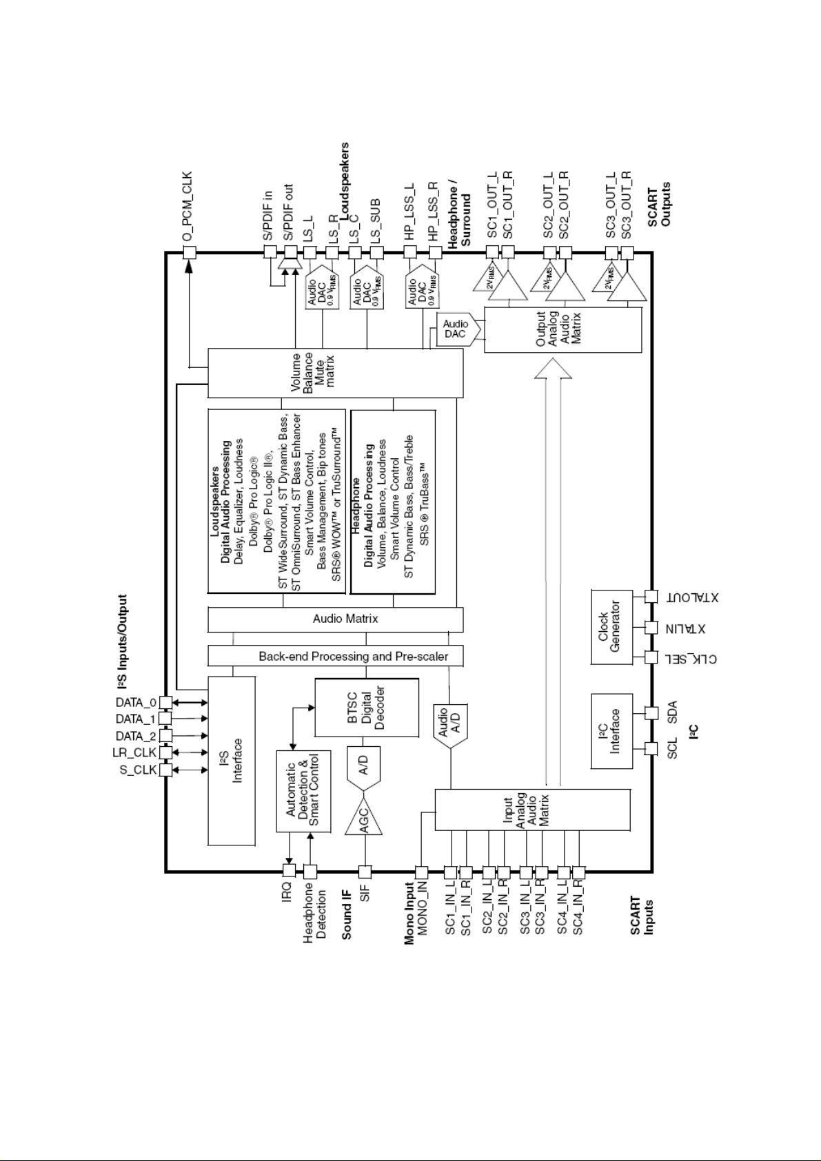
4.STV-8217/STV-8218 brief introduction
STV-8217/STV-8218 is capable of following functions:
15
Page 17

■ Full-Automatic Multi-Standard Demodulation
● B / G / I / L / M / N / D / K Standards
● Mono AM and FM
● FM 2-Carrier and NICAM/BTSC
■ Sound Processing: Loudspeaker
● ST royalty-free processing: ST WideSurround, ST
OmniSurround (Virtual Dolby Surround and
Virtual Dolby Digital compliant) and ST Dynamic
Bass
● Independent Volume / Balance
● Smart Volume Control (SVC), 5-band equalizer and
Loudness
■ Analog Audio Matrix
● 4 stereo inputs
● 3 stereo outputs
● THRU mode
● 2 VRMS capability
Pin introduction:
Pin Designation Function description
1 SC1_OUT_L SCART1 left audio output
2 SC1_OUT_R SCART1 right audio output
3 VCC_H +8V power
4 GND_H ground
5 SC3_OUT_L SCART3 left audio output
6 SC3_OUT_R SCART3 right audio output
7 VCC33_SC +3.3V power
8 GND33_SC Ground
9 SC1_IN_L SCART1 left audio output
10 SC1_IN_R SCART1 right audio output
11 VREFA Sound bypass voltage decoupling interface
12 GND_SA Ground
13 VBG Sound sideband voltage decoupling interface
14 SC2_IN_L SCART2 left audio input
15 SC2_IN_R SCART2 right audio input
16 VCC33_LS DACs power(+3.3V)
17 GND33_LS DACs ground
18 SC2_OUT_L SCART2 left audio output
19 SC2_OUT_R SCART2 right audio output
16
Page 18

VCC_NISO
NISO polarization voltage(+3.3V)
20
GND_SA
DACS ground
21 VSS33_CONV DAC ground
22 VDD33_CONV DAC power (+3.3V)
23 SC3_IN_L SCART3 left audio input
24 SC3_IN_R SCART3 right audio input
25 SCL_FLT SCART left channel filtering
26 SCR_FLT SCART right channel filtering
27 LS_C No connection
28 LS_L Loudspeaker left channel output
29 LS_R Loudspeaker right channel output
30 LS_SUB No connection
31 HP_LSS_L No connection
32 HP_LSS_R No connection
33 VSS18_CONV DAC/ADC ground
34 VDD18_CONV DAC/ADC power (8V)
35 /HP_DET Earphone connection test terminal
36 ADR_SEL Chip address selection signal
37 VSS18 Digital ground
38 VDD18 +1.8V power
39 SCL I²C bus clock
40 SDA I²C bus
41 VSS18 Digital ground
42 VDD18 +1.8V power
43 /RST Reset signal input/output terminal
44 S/PDIF_IN No connection
45 S/PDIF_OUT No connection
46 VDD33_IO1 +3.3V power
47 VSS33_IO1 Digital ground
48 CK_TST_CTRL Digital ground
49 VSS18 Digital ground
50 VDD18 +1.8V Power
51 CLK_SEL Clock input format selection
52 XTALIN_CLKXTP
Oscillator interface
53 XTALOUT_CLKXTM
17
Page 19

54 VCC18_CLK1 5V regulated output
55 GND18_CLK1 Ground
56 GND18_CLK2 Ground
57 VCC18_CLK2 +1.8V Power
58 VSS33_IO2 Digital ground
59 VDD33_IO2 +3.3V Power
60 I2S_PCM_CLK No connection
61 I2S_SCLK I²S clock I/O channel1,2,3
62 I2S_LR_CLK I²S selection signal input/output
63 I2S_DATA0 I²S bus data input/output stereo channel 1
64 I2S_DATA1 I²S bus data input stereo channel 2
65 I2S_DATA2 I²S bus data input stereo channel 3
66 VDD18 +1.8V Power
67 VSS18 Ground
68 BUS_EXP Bus extension selection
69 IRQ No connection
70 GND_PSUB Ground
71 VDD18_ADC +1.8V Power
72 VSS18_ADC Ground
73 SIF_P Intermediate audio input (positive terminal)
74 SIF_N Intermediate audio input (negative terminal)
75 GNDPW_IF Ground
76 VCC18_IF +1.8V Power
77 GND18_IF Ground
78 MONO_IN High frequency head audio input
79 SC4_IN_L SCART4 left audio input
80 SC4_IN_R SCART4 right audio input
STV-8217 internal block diagram:
18
Page 20

19
Page 21
STV-8218 internal block diagram:
5.TDA8944J brief introduction:
TDA8944J is a dual channel sound power amplifier, with each channel has 7W power output
(the resistance of the loudspeaker is 8Ω) to drive the loudspeaker; When music is played, its
high efficiency could reduce external heat dispersion and the requirement of the power supply
equipment.
Its main features:
20
Page 22

● High integration
● Standby and mute mode
● No switch switching noise
● 12V Power filtering
● Low working current
● Output current short-circuit grounding protection
● Overheat protection
● Linear output to drive external earphone, PC and portable audio equipment
Pin introduction:
Pin Designation Function description
1 OUT1 Loudspeaker negative pole output terminal 1
2 GND1 Ground
3 VCC1 +12V Power
4 OUT1 Loudspeaker positive output terminal 1
5 N.C. No connection
6 IN1 Positive pole input terminal 1
7 N.C. No connection
8 IN1 Negative pole input 1
9 IN2 Negative pole input 2
10 MODE Operation mode selection (standby, mute, work)
11 SVR Voltage decoupling filtering (grounding)
12 IN2 Positive pole input terminal 2
13 N.C. No connection
14 OUT2 Loudspeaker negative output terminal 2
15 GND2 Ground
16 VCC2 +12V Power
17 OUT2+ Loudspeaker positive output terminal 2
TDA8944J internal block diagram:
21
Page 23

6. ANX9011L brief introduction:
ANX9011L is a processor used for HDMI (high definition multimedia interface) signal
reception processing, and is used in digital TV, platform screen TV, and projection equipment. It
receives the HDMI input data series and decodes them into digital audio and digital video signal.
ANX9011L could input and output 8 channels digital audio channel of 192kHz sampling
frequency, it has 128 pins with LQFP packaging and has a build-in HDCP, which could greatly
reduce design complexity and system cost.
Its main features are:
● Support up to 165MHz HDMI data rate
● Suitable for HDMI 1.1,HDCP 1.1 and DVI 1.0 format
● Support 20m connection cable
● Support multi-format video processing
24 bit RGB / YCbCr 4:4:4
16/20/24 bit YCbCr 4:2:2
8/10/12 bit YCbCr 4:2:2 (ITU BT656)
12bit two data rate interface
24/48 bit single data rate interface
● RGB and YcbCr color format conversion of each other
● Auto configure video mode
● Digital audio interface
32-192kHz audio sampling rate
Provide 4-channel IIS interface for 8 audio channels
Mute software configuration
● HDCP decryption technology
● PRBS31 link auto-test technology
● Controllable Power protection management system
● 128 pin LQFP packaging
22
Page 24

Pin function
Pin Designation Function description
Digital image output terminal
92 VDE23
┆ ┆
96 VDE19
99 VDE18
┆ ┆
101 VDE16
┆ ┆
105 VDE12
24bit(DP0~DP23)digital video output data bus
108 VDE11
┆ ┆
117 VDE4
121 VDE3
┆ ┆
124 VDE0
2 VDO23
┆ ┆
5 VDO20
8 VDO19
┆ ┆
11 VDO16
14 VDO15
┆ ┆
17 VDO12
20 VDO11
24bit(QO0~QO23)no connection
┆ ┆
23 VDO8
26 VDO7
┆ ┆
29 VDO4
32 VDO3
┆ ┆
35 VDO0
119 VD_CLK Video output data clock
127 DE Video output data effective level signal
128 HSYNC Line synchronizing signal
1 VSYNC Field synchronizing signal
Digital audio output terminal
85 XTAL_IN
Crystal oscillator interface
84 XTAL_OUT
79 MCLKOUT Audio main control clock output
23
Page 25

76 IIS_SCK IIS bus clock
75 IIS_WS IIS signal selection
74 IIS_SD0 IIS bus data
┆ ┆
71 IIS_SD3
IIS channel selection (no connection)
70 SPDIF (no connection )
67 MUTEOUT Mute control signal (no connection )
Control signal port
91 INT Interrupt request output
89 RESETN Reset signal input
42 DDC_SCL DDC Clock signal
41 DDC_SDA DDC address/data signal
40 CFG_SCL I²C bus clock
39 CFG_SDA I²C address/data
90 HDMI_DET Synchronization detection
38 DEVAD I²C connection detection signal
44 HDMI_5V Cable insert detection terminal
88 RESDL Ground
43 NC
45 NC
No connection
HDMI 信号 input terminal
51 HDMI_CLKP
Differential clock input
50 HDMI_CLKN
55 HDMI_D0P
Differential data input1
54 HDMI_D0N
59 HDMI_D1P
Differential data input 2
58 HDMI_D1N
63 HDMI_D2P
62 HDMI_D2N
Differential data input 3
Power and ground
DVDD18
DVDD33
AVDD33
DVSS
12, 24, 36, 51, 66,
81, 82, 112, 125
7, 19, 31, 68, 77,
98, 107, 120
47, 49, 53, 57, 61,
86, 87
6, 13, 18, 25, 30,
37, 65, 69, 78, 80,
97, 106,
+1.8V digital Power
+3.3V digital Power
+3.3V analog Power
Digital ground
113, 118, 126
AVSS 46, 52, 56, 60, 64,
83
Analog ground
ANX9011L internal block diagram:
24
Page 26

7. 74HCT4052D brief introduction:
74HCT4052D is a 4-channel bi-directional analog multiplexer and multi-channel output
selector. Each multi-channel output selector has 4 independent input/output terminals and 1
common input/output terminal. It is often used in analog and digital multiplexing, and
multi-channel output selecting circuit and signal control system.
Its main features are:
● -5V to +5V widely range Power input
● Low on-resistance
● Logical level alternating
● Build-in interrupt before running
● In line with JEDEC 中 no.7A standard
● Automatic protection function
Pin introduction:
Pin Designation Function description
1 2Y0 PC left audio input
2 2Y2 HD terminal left audio input
3 2Z Left audio input
4 2Y3 SCART2 left audio input
5 2Y1 AV left audio input
6 E Ground
7 VEE Ground
8 GND Ground
9 S1
Select level input (+3.3V Power)
25
Page 27
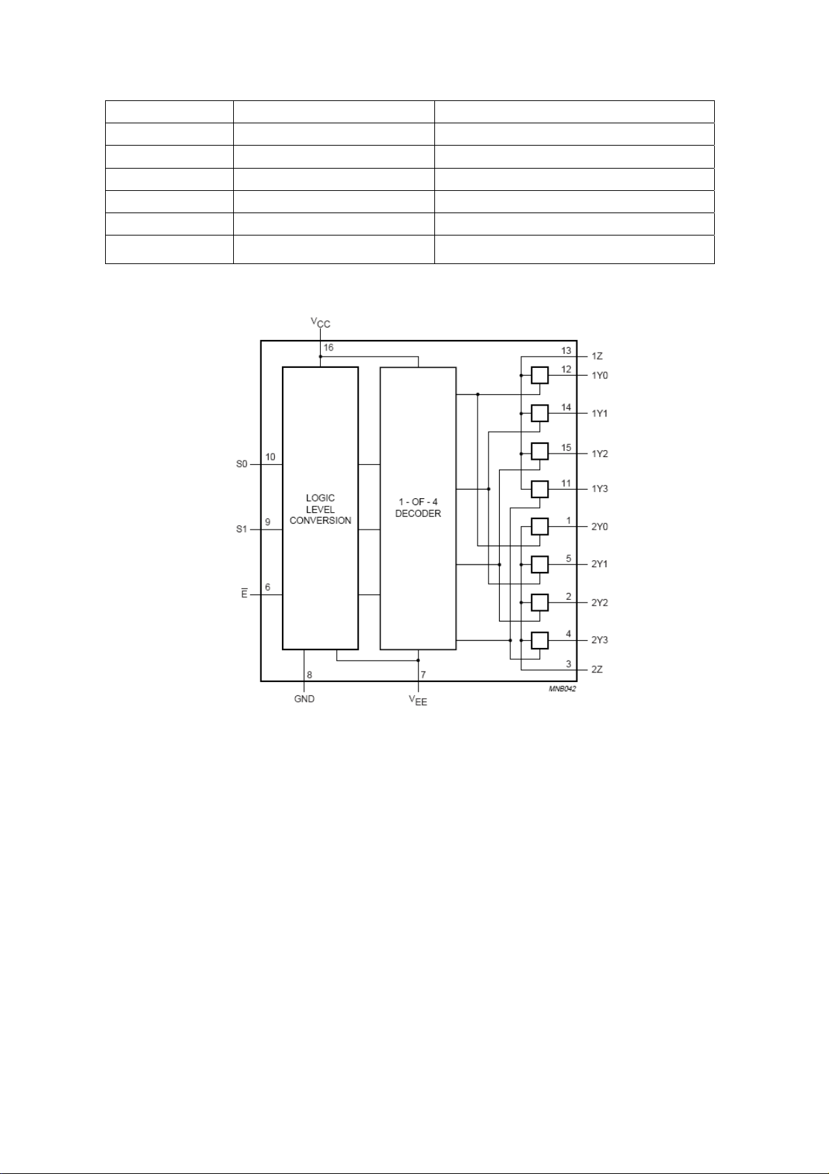
10 S0
11 1Y3 SCART2 right audio input
12 1Y0 PC right audio input
13 1Z Right audio output
14 1Y1 AV right audio input
15 1Y2 HD terminal right audio input
16 VCC +5V Power
74HCT4052D internal block diagram:
26
Page 28

Chapter 3 Whole Machine Signal Processing Analysis and
,
Measured Data at the Key Points
This chapter Mainly introduces the receiving and processing of image signal and sound
signal, whole machine system control process, and whole machine power supply system
(Model of LTA-32C904 is taken as an example, other models is similar and will not be explained
here for each. There are minor differences in power supply among different models of liquid
crystal screen; the details are shown in Specifications).
1. Image signal flow
RF signal is demodulated by tuner, then the obtained video signal and signals inputted from
COMPONENT terminal, AV terminal, S terminal, 2-way Scart interface and VGA interface are all
sent into video-processing IC SVP-CX32LF to be processed. Input signals with different format
are changed into uniform LVDS differential signals, and are sent to liquid crystal screen. In
addition, TV video signal is processed by SVP-CX32LF to generate 2-way CVBS signal, which
is used in 2-way Scart video output.
Signal inputted from HDMI interface is decoded into digital video signal, which is sent into
video decoding IC SVP-CX32LF to be processed. After procession, the obtained uniform LVDS
differential signal is sent to liquid crystal screen through LVDS interface to screen.
2.Sound flow
RF signal is demodulated by tuner, and then the obtained SIF signal (SIF-2 signal) and
audio signal inputted from Scart1 interface are directly processed by STV-8217. The output
audio signal of STV-8217 is sent into power amplifier TDA8944J, and the amplified signal is
finally sent to speaker or earphone output.
Signals from HDTV terminal, AV terminal, Scart2 interface and PC Audio are first sent into
74HCT4052D for choosing passages, and then sent into STV-8217 for demodulation and sound
effect processing. The output audio signal of STV-8217 is sent into power amplifier TDA8944J,
and finally the amplified signals are sent to speaker or earphone output.
After the demodulation and sound effect processing of STV-8217, there is an audio output
which is used for sound output of Scart1 terminal.
3. Whole machine power supply system
There are 4 ways of voltage output in the power panel: +24V(6A)、+12V(2A)、+5V(2A)
and +5VS(1A). +24V output is used by LCD screen; +12V output is used by power amplifier
TDA8944J, and is also changed into +8V output by AZ78L08ZTR-E1 to satisfy the need of
STV-8217 IC; +5V output is changed into 1.8V output and 3.3V output by DO (such as
AZ1117H-1.8TRE1 and AZ1117H-3.3TRE1) to satisfy the needs ICs. +24V, +12V and +5V
outputs will be cut off in standby state. While +5VS output is the power supply of MCU, infrared
receiver and EEPROM etc, and will be cut off when the AC is turn off.
5V output will be divided into two ways: one way is changed into +3.3V and +1.8V analogue
power supplies through DC/DC converter for STV-8217 IC, ANX9011LF IC etc and peripheral
circuits; other way is changed into +3.3V and +1.8V digital power supplies through DC/DC
converter for SVP-CX32 IC etc and peripheral circuits, and this way of 5V voltage will be cut off
in standby state, while the other way of 5V voltage supply power especially for MCU, infrared
receiver and EEPROM etc, and will not be cut off in standby state.
(1) Constitution and distribution of whole machine power supply
+12V power
supply
FB34
CON11
Pin 1,2,3
FB8
+12V power
FB34
27
supply
CON403
Pin 3
12V power amplifier TDA8944J
4
U23
AZ78L08ZTR-E1
12V
+12V(voltage of line to screen) CON1
Pin 1,2,3,4 (used by 37 inches screen)
Pin 3,16
12V shutdown mute circuit
8V
ST82X7
Pin 3
Page 29

(
,
,
,
,
)
,
,
,
20
2
A
108
S
3
3
1
3
3
,16,20,
R206
2.2mA
FB27
U18
CX_VA18
1.8V
R3,R4
AZ1117H-1.8TRE1
R213 FB1,FB2
CX_VL18
1.8V
U1 SVP-CX32
Pin 177
178,186,193
U30 Sil9011
Pin 12, 24, 36, 51, 66,
82, 112, 125
81
U1 SVP-CX32
Pin 200
202,208,3
FB26 FB29
FB23 FB30,32
R214
575m
FB
FB5,6
5V
FB22 FB4
11
10
9
L1,2
8
V
.
+
TRE
.
4
U20 AZ
Pin 7, 19, 31, 68, 77, 98, 107, 120
Pin 47, 86, 87
U30 Sil9011
Pin 49, 53, 57, 61
U30 Sil9011 pin 87,86
U21
AZ1084S-1.8TRE1
U1 SVP-CX32 Pin 19,72
U1 SVP-CX32 Pin 165,166
U1 SVP-CX32 Pin 46, 39, 52
U1 SVP-CX32 Pin 155,156
U30 Sil9011
U1 SVP-CX32
Pin 12,27,53,74,96,
119,136,160
FB3
CON11 Pin 7
Pin 1,15,29,43,3,9,35,41,49,55,75,81
U2 IS42S32200C1-6TL
R2
+5V
U1 SVP-CX32 Pin 98, 108, 134,146
FB21
L24
U35 ST8217
Pin 7
22
L21
U35 ST8217 Pin 46
L28,29,22
AZ1117H-1.8TRE1
U22
+1.8V
U35 ST8217 Pin51
U35 ST8217 Pin 42,76,54
U19 AZ1117H-3.3TRE1 +3.3V
28
Page 30

(
,
,
,
,
)
Y4 27MHz XO voltage
U9 74HCT4052D Pin 16
FB12
Starting up mute circuit
FB16
FB24
11
FB17
10
9
FB7
8
FB20
+5V(voltage of line to screen)CON1 Pin 1,2,3,4 (used by
screen less than 32 inches)
U15 JS-6B2/121 Tuner Pin 3
U15 JS-6B2/121 Tuner Pin 13
R232
R198
CON11 Pin7
R202
+5V
U30 Sil9011 Pin 44
Back light switch control
Back light height control
CON13
Pin 4,3
FB28
U26 CS4344-CZZ Pin 9
U14 U16,25 U31 U28,29
74LVC14AD AT24C02BN PI5C3306LE 0514M.TBT
Pin 14 Pin 8 Pin 8 Pin 3
U1(SVP-CX32)Pin 85,D7,8(BAV99L)Pin 2
J3 VGA terminal interface voltage
FB19 R207
R208
IIC Bus data interface
IIC Bus clock interface
CON4, CON 15, CON 16
Pin 2,3
5V_SB(CON12 Pin1,2)
FB9
FB25
FB10
AZ1117H-3.3TRE1
U24
+1.8V
FB11
U4 T5BS4-9999
Pin 64
U5 SST39VF040
Pin 32
U4 T5BS4-9999
Pin 18
CON14 Pin 1
CON17 Pin 1
CON5 Pin 1
U3(AT24C64A-10PU-2.7)Pin 8
TCM809SENB713) Pin 3
U8(
74ALVC573PW) Pin 20
U6(
Q8、9(2SK1399) Pin1
Q10、11(2SC1815M-Y) Pin1
29
Page 31

(3) Pin level schedule for Voltage regulators on mainboard
Position
Component model Pin 1(V) Pin 2(V) Pin 3(V)
number
U18、U22
U19、U24
AZ1117H-1.8TRE1 GND 1.8V 3.3V
AZ1117H-3.3TRE1 GND 3.3V 5V
U20 AZ1084S-3.3TRE1 GND 3.3V 5V
U21 AZ1084S-1.8TRE1 GND 1.8V 3.3V
U23 AZ78L08ZTR-E1 12V GND 8V
(4) Pin sequence of power cord of power panel
Position
Pin Pin definition Pin function discription
number
1 ON/OFF
L:OFF ;H:ON
2,3 GND GND
4,5 5V +5V/4A
CON1
6 5Vstb +5V/1A
7,8 GND GND
9,10 12V +12V/1A
1,2 12VA +12V/2A
CON2
3,4,5,6 GND GND
7,8 24Vio +24V/1A
1,2,3 GND GND
CON3
4,5,6 24VI +24V/4A
4. Position and definition of the main components and sockets on mainboard
30
Page 32

31
Page 33

(1) Socket definition
e
Serial
number
1 CON40
Position
number
Connecting object Function description
Power panel GND,GND,+12V,+12V
3
2 CON11 Power panel +12V,+12V,+12V,GND,GND,GND,+5V,
+5V,+5V,+5V,+5V
3 CON13 Back light control line GND,GND,back light switch control,back light
brightness control
4 CON14 Keyboard +3.3V、GND、KEY1、KEY2
5 CON17 Remote control
+3.3V、REMOTE、GND、indicator1、indicator1
receiving board
6 CON4 Standby
7 CON5 Standby
8 CON1 LVDS interface of line
to screen
9 CON15 I²C
10 CON12 Power panel +5V_SB , +5V_SB , GND , GND , Power supply
control
11 CON13 Standby
12 CON8 Standby
13 CON9 Speaker L+,L-,R+,R-
14 CON10 Side AV board
15 J9 VGA audio signal input
16 J8 SCART2 input
17 J5 SCART1 input
18 J4 HDMI input
19 J2 HD, audio, video
signal input
20 J6 S terminal input
21 J3 VGA input
22 CON2 Standby
(2) Main components descriptions
Serial
numb
Position
number
component Function description
r
A
B
C
D
E
F
32
U16 AT24C02BN-10SU-1.8 EEPROM
U14 74LVC14AD
U2 IS42S32200C1-6TL
VGA line and field synchronizing signal
shaping
2MX32bits SDRAM, used for video signal
access
U3 AT24C64A-10PU-2.7 EEPROM
U8 TCM809SENB713 MCU reset IC
U31 PI5C3306LE I²C bus switcher for program upgrading
Page 34

G
H
I
J
K
U18、U21、U22 AZ1117H-1.8TRE1 3.3V to 1.8V DC-DC Converter
L
M
N
O
P
Q
R
S
T
U
V
U1 SVP-CX32LF
U5
SST39VF040-70-4C-N
HE
U4 T5BS4-9999 MCU,mainly control IC
U6 74ALVC573PW
U20 AZ1084S-3.3TRE1 5V to 3.3V DC-DC Converter
U19 、U24 AZ1117H-3.3TRE1 5V to 3.3V DC-DC Converter
U23 AZ78L08ZTR-E1 12V to 8V DC-DC Converter
U26 CS4344-CZZ
U30 ANX9011L
U25 AT24C02BN-10SU-1.8 EEPROM
U28、U29 Rclamp0514M.TBT HDMI signal ESD protective device
U35 STV-8217 Sound Processor
U9 74HCT4052D AV input sound passage switcher
U33 TDA8944J 2X7W Sound Amplifier(BTL Output)
U15 JS-6H2/121 Tuner
Video decoding, image processor, A/D and
D/A conversion
Flash MEMORY , storing whole machine
control program
Address latch,for latching and extending the
address line
HDMI digital audio decoding and D/A
conversion
HDMI decoding, HDTV video/audio
reproduction
5. Waveforms at key points
(1)RF inputting color bar signal, Composite Video Signal waveform at pin 14 of tuner U15, the
waveform at pin 169 of U1(SVP-CX32LF) is alike:
(2)RF inputting color bar signal, I²C bus clock signal SDA, pin 5, 6 of U31, pin 6 of U16, pin 39
of U35, pin 58 of U4, pin 40 of U30, pin 57 of U1, pin 4 of tuner U15:
33
Page 35

(3) RF inputting color bar signal, I²C bus clock signal SDA, pin 2, 3 of U31, pin 5 of U16, pin 40
of U35, pin 57 of U4, pin 39 of U30, pin 58 of U1, pin 5 of tuner U15:
(4)RF inputting grey signal, Composite Video Signal waveform at pin 14 of tuner U15, the
waveform at pin 169 of U1(SVP-CX32LF) is alike:
34
Page 36

(5)RF inputting white signal, SIF Signal waveform at pin 11 of tuner U15, and waveform at pin
73 of sound effect processing IC Stv-8217:
(6)RF inputting white signal, and inputting sound signal with 1KHz frequency, inductance
waveforms at pin 28, 29 of U35, and waveform of L26,L27:
35
Page 37

(7)Inputting sound signal with 1KHz frequency, with the processing of U33 and power amplifier
TDA8944J, waveform at pin 1, 4, 14, 17 of U33, and waveform at CON13 speaker and
CON14earphone output interfaces:
36
Page 38

Chapter 4 Familiar Problem and Processing
1.Failure phenomenon:The picture is normal,but OSD has line in it.
The reason and the processing:Check the pin of U2 and pin 80-160 of U1 for pseudo
soldering, and have pseudo soldering touched up.
2.Failure phenomenon:There is sound but no picture; there is no OSD when start up; and
the back light is bright.
The reason and the processing:Check the connecting line to screen, and have it
connected well.
3.Failure phenomenon:There are no picture, no sound, and no snow flower dot in TV
mode, but AV is normal.
The reason and the processing:Check the tuner and its peripheral circuits (including bus
and power supply). If the peripheral circuits work well but there is no output from tuner,
then the tuner must be failure.
4.Failure phenomenon:LCD television cannot be controlled(including no starting up with
red light on, remote control and local key having no effect, etc).
The reason and the processing:LCD television has crash phenomenon, restart after
power off.
5.Failure phenomenon:+5V_SB voltage has output, but there are no picture, no sound,
and back light and indicating light are not on.
The reason and the processing:Check other groups of voltage; if they have no outputs,
then check Flash to find if it is installed well or damaged; if Flash is OK, find out that if the
power supply and output voltage of U4 works well.
37
Page 39

Chapter 5 Listing of Repair and Easily Damaged Parts
This listing of maintenance and repair parts are presented for reference only,
modification of parameters will not be informed. For accurate models or specifications,
please consult the newest data of our company. (32 inches series is taking as example)
Proportion of easy
Number Name Part code Part number Print plate number
1. Panel frame JUG6.116.623
2. Back cover JUG6.116.624 0.1
3. Mount part JUJ7.356.005 0.1
4.
Mainboard part JUG6.690.106
Remote receiving
5.
board part JUG6.695.028
6.
Keyboard part JUG6.694.029
Inner power
7.
module FSP205-5E01 Inner power module
Print plate
JUG7.820.015 1
Print plate
JUG7.820.016 0.5
Print plate
JUG7.820.017 0.5
damage
(‰)
0.1
5
8.
LCD screen V320B1-L04 LCD screen
9. Electronic tuner JS-6H2/121 Electronic tuner 1
10.
Electronic tuner
11.
Dynamic speaker
12.
Dynamic speaker
Remote control
13.
emitter
GK23J2
CDT-6GPL22-0
0
YDT613-A9-10
W-8Ω
YDG52-A3-10W
-8Ω
Electronic tuner
Dynamic speaker
Dynamic speaker
Remote control
emitter
0.1
1
2
2
1
38
Page 40

Chapter 6 Factory Mode Setting and Items Needs Attention
r
r
r
r
1. Enter factory menu
Power on TV set, and make LCD at working state:
① Press 【MUTE】 key on remote control;
② Press “MENU” key on remote control, and switch to “SOUND” option with
【V+】,【V-】key;
③ Move cursor to “Balance” option with 【P+】,【P-】key to enter setting status;
④ Press number key “3”、“1”、“3”、“8”on remote control to enter password.
Entering factory mode is then finished. Press【Display】key to quit factory mode.
⑴ Factory menu display is presented like bellow:
chassis:Ls01
Jul 29 2006 23:25:16
Version:LsE01-M32-V1.05WL
I²C off
Clear E²PROM
Panel Control
Factory Setting
System Control
Min/Max CONTROL
White Balance
Hotel Option
E²PROM Edit
Register Edit
Notes:
“chassis:LS01”is the model number of local module,“Jul 29 2006 23:25:16”
is the latest upgrading time for software, and“Version:LSE01-M32-V1.05WL”is the
version number of current software.
(2)The detailed setting items are given bellow:
Contents of first page:
Setting item Setting content Setting method
IIC Off
Clear EEPROM
Panel Control
Factory Setting Factory Setting
System Control System Control
Min/Max Control
White Balance
Hotel Option Hotel mode
E²PROM Edit
Stop I²C bus
communication
E²PROM
initialization
Screen back light
brightness control
Analog setting of
picture and sound
White balance
setting
E²PROM data
editing
“OK”or“V+”,“V-”key
Press “OK”key first,then
press “V-”key
Press “V+”,“V-”keys to
enter submenu
Press “V+”,“V-”keys to
enter submenu
Press “V+” key to ente
submenu
Press “V+” key to ente
submenu
Press “V+” key to ente
submenu
Press “V+” key to ente
submenu
No setting
Register Edit Register No setting
Remark
Used for updating
program
Only done in first
setting station
Only set sub
brightness
Bri Mid
Used for hotel TV
Use 【P+】and 【P-】keys on remote control to make up or down option, and use【V+】
and【V-】keys to set.
39
Page 41

Contents of sub pages:
Panel Control
Setting item
Setting
value
Remark
LVDS Mapping 0x09 Polarity of LVDS signal
Backlight 100 Back light brightness value 1
SavePower1 50 Back light brightness value 2
SavePower2 30 Back light brightness value 3
BL-invisible Off
Show SavePower mode in menu or not
(ON:not show;OFF:show)
Factory Setting
Setting item Setting value Remark
Balance -50_0_50
Fast check of the balance characteristic of L/R
sound channel
Volume 0_10_20…_100 Fast setting of volume,each step is 10
IIS On/Off Preset sound decoding IC of HDMI
Def Country Other Default country
RTC En On/Off Show real time clock or not
CANAL-Visual On/Off Open Canal+ function to user or not
System Control
Setting item Setting value Remark
Setting
item
Default Lang English Default OSD language SSC
L/L’ AGC 5 L/L’ sound AGC Delta 0
OverModulation On/Off OverModulation switch Positive 6
PreScl SCART 8
SCART L/R input amplitude
preamplifing
Negative 6
PreScl AM 12 AM_MONO IF preamplifing Write
PreScl FM 12 FM_MONO IF preamplifing
PreScl NICAM 19 NICAM sound IF preamplifing
Equalizer switch , Off is 5 section
EQ-invisible Off
equalization , On is high/low pitch
setting
ATS Off Program auto sequencing switch
Logo Off
Starting blue background LOGO
switch
LOGO display contents,“V+”、“V-”for
Logo Edit Akai
choosing setting position,,“P+”、“P-”
for choosing letter , including 52
English big/small letters together
Logo Colour Logo colour Modified according to user’s require
Setting
value
Min/Max Control
Setting item Setting value Setting item Setting value
Con Min 30H Vol Min 00H
Con Mid 70H Vol Mid 1 01H
Con Max A2H Vol Mid 2 14H
40
Page 42

Bri Min 00H Vol Mid 3 28H
Bri Mid 8DH Vol Mid 4 4BH
Bri Max A0H Vol Max 64H
Col Min 00H Tre Min 00H
Col Mid 40H Tre Mid 30H
Col Max 70H Tre Max 60H
Tnt Min 20H Bas Min 00H
Tnt Mid 80H Bas Mid 30H
Tnt Max E0H Bas Max 60H
Shp Min 00H
Shp Mid 60H
Shp Max A0H
White Balance
Normal Warm
R Gain 7DH R Gain 7DH
G Gain 80H G Gain 80H
B Gain 9AH B Gain 9AH
R Offset 80H R Offset 84H
G Offset 80H G Offset 80H
B Offset 74H B Offset 74H
Cool
R Gain 7DH
G Gain 80H
B Gain 9AH
R Offset 80H
G Offset 80H
B Offset 90H
Hotel Option
Setting item
Setting
value
Hotel Mode Enable No
Remark
Hotel mode presetting(Yes for Hotel Mode,No for normal TV
mode)
Force Pos 1 Forced program number
Force Video ext1 Forced AV input terminal
Disable Keypad No Open local key function or not
Disable Remote No Open remote receiving function or not
Disable Setup Menu No Open “setting” in OSD menu or not
Notes:
A. In“Min/Max CONTROL” setting item, “Bri Mid”item is used to set sub brightness of
picture;
B. White balance needs to be set in “Normal”mode;
C. Set CLEAR E²PROM will clear the memory data, So do not set it unless it is needed;
other setting items do not need setting.
2. Setting method of factory menu
⑴ Choose setting item
41
Page 43

Operators can choose setting item orderly with【P+】and【P-】key, font having background
display represents the item has been chosen. Press【V+】key to enter sub directory. Use
【P+】and 【P-】keys on remote control to make up or down option, and use【V+】and
【V-】keys to set.
(2)All the menu functions are opened in factory mode, item checking and effect testing
can be done by using menu if it is needed.
(3)Switching TV program number in factory mode can be done by directly pressing the
number key. Press【MENU】key to back to the parent of working directory, press
【DISPLAY】key to quit factory mode.
42
Page 44

Appendix 1
LS01 module(taking LTA-32C904 for example)Schematic Diagram
43
Page 45

44
Page 46

45
Page 47

46
Page 48

47
Page 49

48
Page 50

Appendix 2
Power Module Schematic Diagram
49
 Loading...