

Page 1
TV-AN2010
NH
SERVICE MANUAL
COLOR TELEVISION
This Service Manual is the "Revision Publishing" and replaces "Simple Manual"
(S/M Code No. 09-003-340-3T1).
S/M Code No. 09-003-340-3R1
REVISION
DATA
Page 2
NOTICES BEFORE REPAIRING
To make the best use of this equipment, make sure to
obey the following items when repairing (or mending).
1. Do not damage or melt the tunicate of the leading
wire on the AC1 side, including the power supply
cord.
2. Do not soil or stain the letters on the spec.
inscription plates, notice labels, fuse labels, etc.
3. When repairing the part extracted from the
conducted side of the board pattern, fix it firmly
with applying bond to the pattern and the part.
4. Restore the following items after repairing.
1) Conditions of soldering of the wires (especially,
the distance on the AC1 side).
2) Conditions of wiring, bundling of wires, etc.
3) Types of the wries.
4) Attachment conditions of all types of the insulation.
5. After repairing, always measure the insulation
resistance and perform the voltage-withstand test
(See Fig-1).
1) The insulation resistance must be 7.0 to 9.5 MΩ
when applying 500V per second.
2) In the voltage withstand test, apply 1.0 kV for 1
minute and check that the GO lamp lights.
Insulation resistance: 7.0 to 9.5 MΩ (500 V/s)
Voltage-withstand: 1.0 kV for 1 minute.
Safety checker (Model7110,etc.)
Earth cable
AC cable
Connect the earth cable
to the outside metal part
terminal.
Fig-1
* Breaking current set to 10 mA.
* Connect the safety checker as shown in Fig-1,
then measure the resistance and perform the test.
* Do not touch the equipment during testing.
* For details of the safety checker, refer to the supplied
Operation manual.
When servicing and checking on the TV, note the followings.
1. Keep the notices.
As for the places which need special attentions, they
are indicated with labels or seals on the cabinet,
chassis and parts. Make sure to keep the indications
and notices in the operation manual.
2. Avoid an electric shock.
There is a high voltage part inside. Avoid an electric
shock while the electric current is flowing.
3. Use the designated parts.
The parts in this equipment have the specific
characteristics of incombustibility and withstand voltage
for safety.
Therefore, use a part which has the same character
as the replaced part. Especially as to the important
parts for safety which is indicated in the circuit
diagram or the table of parts with a mark, the
designated parts must be used.
4. Put parts and wires in the original position after
assembling or wiring.
There are parts which use the insulation material such
as a tube or tape for safety, or which are assembled so
that these parts do not make contact with the printed
!
board. The inside wiring is designed not to get close to
the pyrogenic parts and high voltage parts. Therefore,
put these parts in the original positions.
5. Take care of the cathode-ray tube.
By setting an explosion-proof cathode-ray tube in this
equipment, safety is secured against implosion.
However, when removing it or servicing from the
back, it gives out shock that is dangerous. Take
enough care to deal with it.
6. Avoid an X-ray.
Safety is secured against an X-ray by giving
considerations to the cathode-ray tube and the high
voltage peripheral circuit, etc. Therefore, when
repairing the high voltage peripheral circuit, use the
designated parts and do not change the circuit.
Repairing, except indicates, causes rising of high
voltage, and the cathode-ray tube emits an X-ray.
7. Perform a safety check after servicing.
Confirm that the screws, parts and wiring which were
removed in order to service are put in the original
positions, or whether there are deteriorated portions
around the places serviced.
2
Page 3

SPECIFICATIONS
Tuner System Frequency synthesized tuner
TV System NTSC-M
Channel Coverage VHF: 2 to 13
Program Memory 181
Antenna Input 75 ohms, unbalanced
Picture Tube 20’’
Screen Size 404 (W) x 303 (H) mm (16 x 12 in.)
Video Input 1 Vp-p 75 ohms
Audio Input 0.5 Vrms., 33 k ohms more
Speaker 120 x 60 mm (43/4 x 2 3/8 in.)
Operating Voltage 110 - 240 V, 50/60 Hz
Power Consumption 105 W
Phone Jack Stereo-mini jack
Operating Temperature 5°C - 40°C
Operation Humidity 35% - 80%
Dimensions 610 (W) x 440 (H) x 483 (D) mm
Weight 19.5 kg (42.9 lbs.)
• Design and specifications are subject to change without notice.
UHF: 14 to 69
CATV: 5A, A-1 to A-5, A to W, W+1 to W+84
480 mm (Visible diagonal) (19 in.)
1
(24
/8 x 173/8 x 191/8 in.)
ACCESSORIES LIST
REF. NO PART NO. KANRI DESCRIPTION
1 8Z-JAK-901-010 IB,NH (E) -AN2110/ 2010/1410
2 8Z-JAE-951-010 RC UNIT,RC-ZVT18
3 87-A90-702-010 ANT ASSY,TV 5 SEC (NTSC)
! 4 87-A91-015-010 PLUG,CONVERSION JT-0475A
NO.
3
Page 4
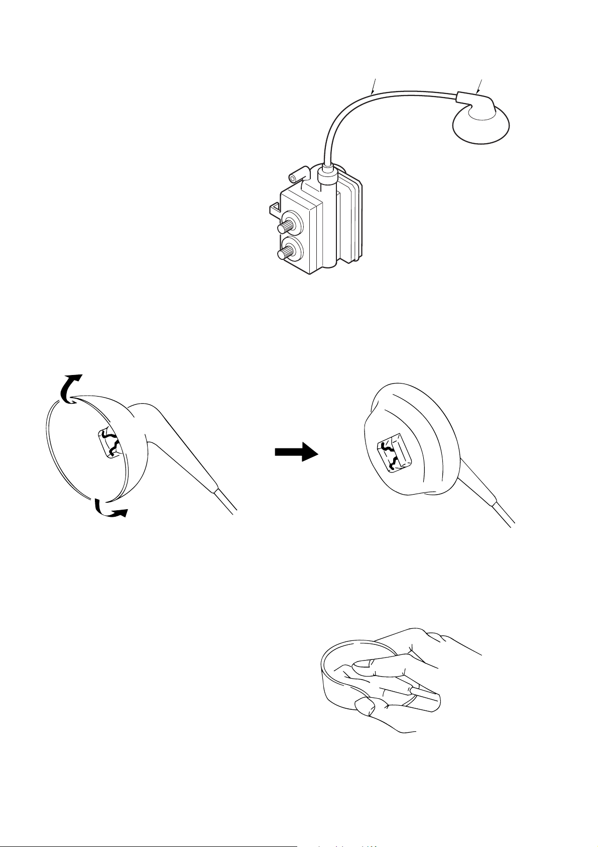
Anode cap
CRT GND
Hook
CRT
CRT GND
Grip
DISASSEMBLY INSTRUCTIONS
Front cabinet
Rear cabinet
1. REAR CABINET REMOVAL
(1) Remove four screws 1 and three screws 2, then remove
the rear cabinet in the direction of the arrow. (See Figure1-
1)
2. HIGH-VOLTAGE CAP (ANODE CAP) REMOVAL
Figure 1-1
2-1. Cautions before Removing
Discharge the anode voltage
(1) The anode voltage is not discharged completely from the
CRT of this unit even after the power is turned off. Be
sure to discharge the residual anode voltage before
removing the anode cap.
Do not use pliers
(2) Do not use pliers, etc. to remove the anode cap. If you
used pliers and bent the hook to remove the cap, the spring
characteristics of the hook could be lost, and when
reinstalled, the cap would come off from the CRT anode
button easily, causing an accident.
Do not turn the anode cap
(3) If the anode cap is turned in the direction of its
circumference, the hook is likely to come off.
2-2. Anode Cap Removal
Discharge the anode voltage. (See Figure 2-1)
(1) Connect a flat-bladed screwdriver to the CRT GND via
an alligator clip.
(2) Use a tester to check the end of the screwdriver and ground
of the TV for continuity.
(3) Touch the hook with the end of the screwdriver.
Caution : Be careful not to damage the anode cap.
(4) Turn over the anode cap.
Caution : Be careful not to damage the anode cap.
CRT
Figure 2-1
Anode cap
Anode button
Hook
Figure 2-2
4
Page 5
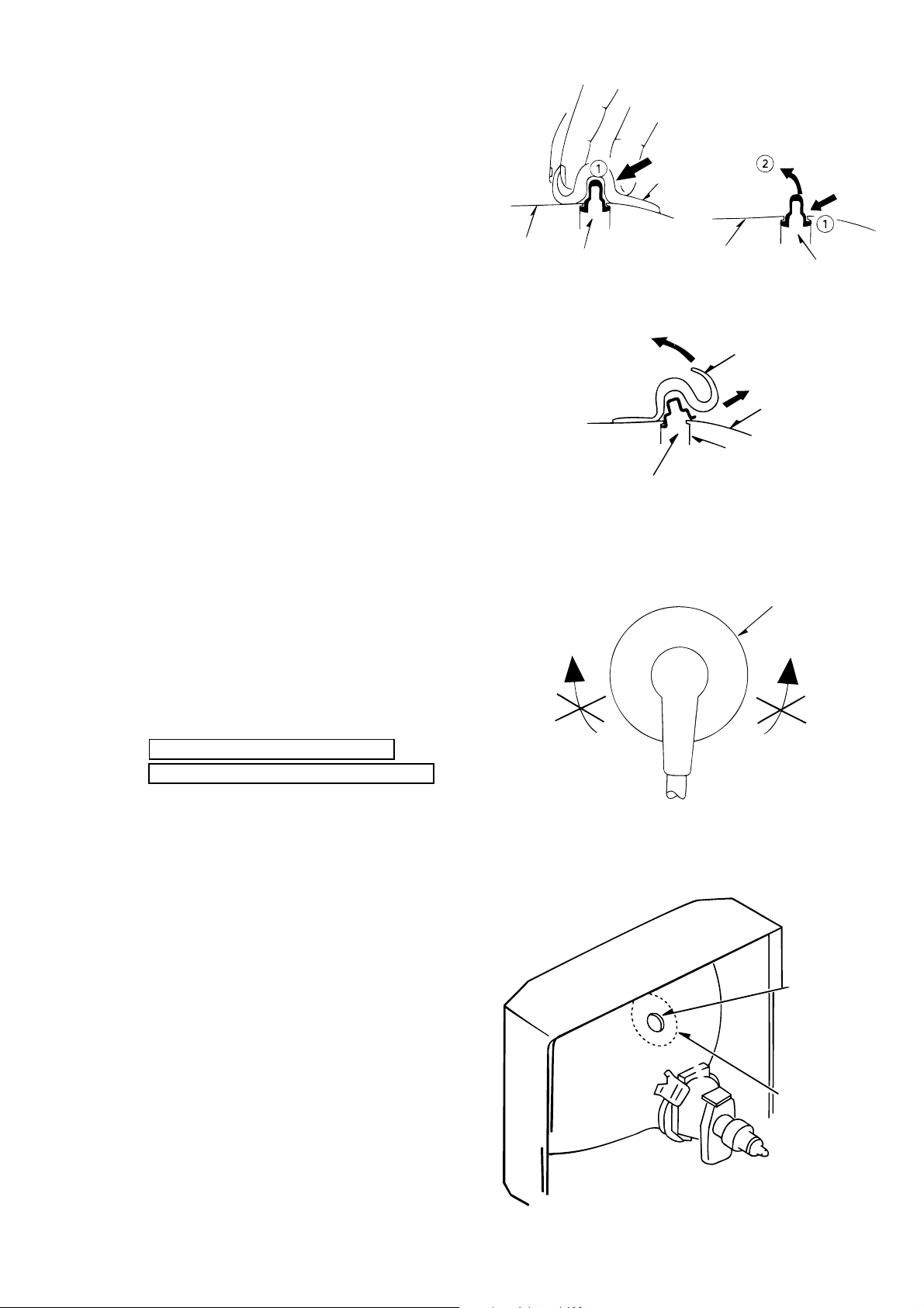
(5) Push the anode cap with your thumb in the direction of
CRT
CRT
Anode cap
Hook
Hook
Anode cap
Hook
Anode button
CRT
Left
Right
Anode cap
Anode button
Installation
section
arrow 1 as shown in the figure, then lift the cap in the
direction of arrow 2 to release the hook on one side. (See
Figure 2-3)
(6) Turn over the anode cap on the side where the hook was
released and pull out the cap in the direction opposite to
that on which the cap was pushed. (See Figure 2-4)
Caution : Do not pull out the anode cap straight up.
: Do not pull the cap forcibly. After removing
the cap, check that the hook is not deformed.
Figure 2-3
Figure 2-4
3. ANODE CAP REINSTALLTION
Observe the cautions carefully so that no accident occurs
due to a defect in installing the anode cap and so it does
not come off.
3-1. Caution before Reinstalling
Never turn the anode cap after installing it
Never re-use the hook when it has been deformed
(1) If the anode cap is turned after it is installed, it may come
off. Therefore, arrange the high-voltage cable before
attaching the anode cap. (See Figure 3-1)
(2) If you have attached the anode cap before arranging the
high-voltage cable, arrange the cable carefully so the cap
does not turn.
3-2. Anode cap reinstallation
(1) Use a clean cloth moistened slightly with alcohol to clean
the installation section. (See Figure 3-2)
Caution : Check that the installation section is free from
dust, foreign matter, etc.
(2) Coat the anode cap installation circumference with an
appropriate amount of the specified silicone grease (KS650N).
Caution : Be careful that silicone grease does not enter
the anode button.
Figure 3-1
Figure 3-2
5
Page 6
(3) Eliminate twisting, etc. of the high-voltage cable and
arrange it so that no twisting occurs. (See Figure 3-3)
Caution : If the cable is not arranged correctly, the anode
cap could turn and cause an installation defect.
(4) Turn over the rubber cap symmetrically on the left and
right. (See Figure 3-4)
Caution : Take great care not to damage the anode cap.
High-voltage cable
Anode cap
Figure 3-3
(5) Fit your forefinger over the projection at the center of the
cap and hold the cap between your thumb and middle
finger. (See Figure 3-5)
Figure 3-4
Figure 3-5
6
Page 7
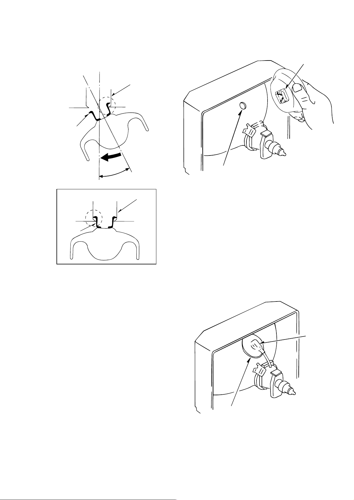
(6) Apply the hook on one side to the anode button as shown
Anode button
Skirt
on the figure. (See Figure 3-6)
Caution : Check that the hook is held securely.
(7) Apply the hook on the other side to the anode button as
shown in Figure 3-7.
Anode button
Hook
Hook
Anode button
30°
Anode button
Hook
Figure 3-7
(8) Pull the anode cap slightly with the rubber cap turned
over and visually check that the hook is engaged securely.
(9) Release your hand from the rubber cap of the anode cap.
Caution : Cover the anode cap so that it does not lift.
(10) Hold the skirt of the andoe cap slightly to improve the
close contact between the cap and CRT.
(11) Check that the anode cap is in close contact with the CRT.
(See Figure 3-8)
Figure 3-6
Figure 3-8
7
Page 8
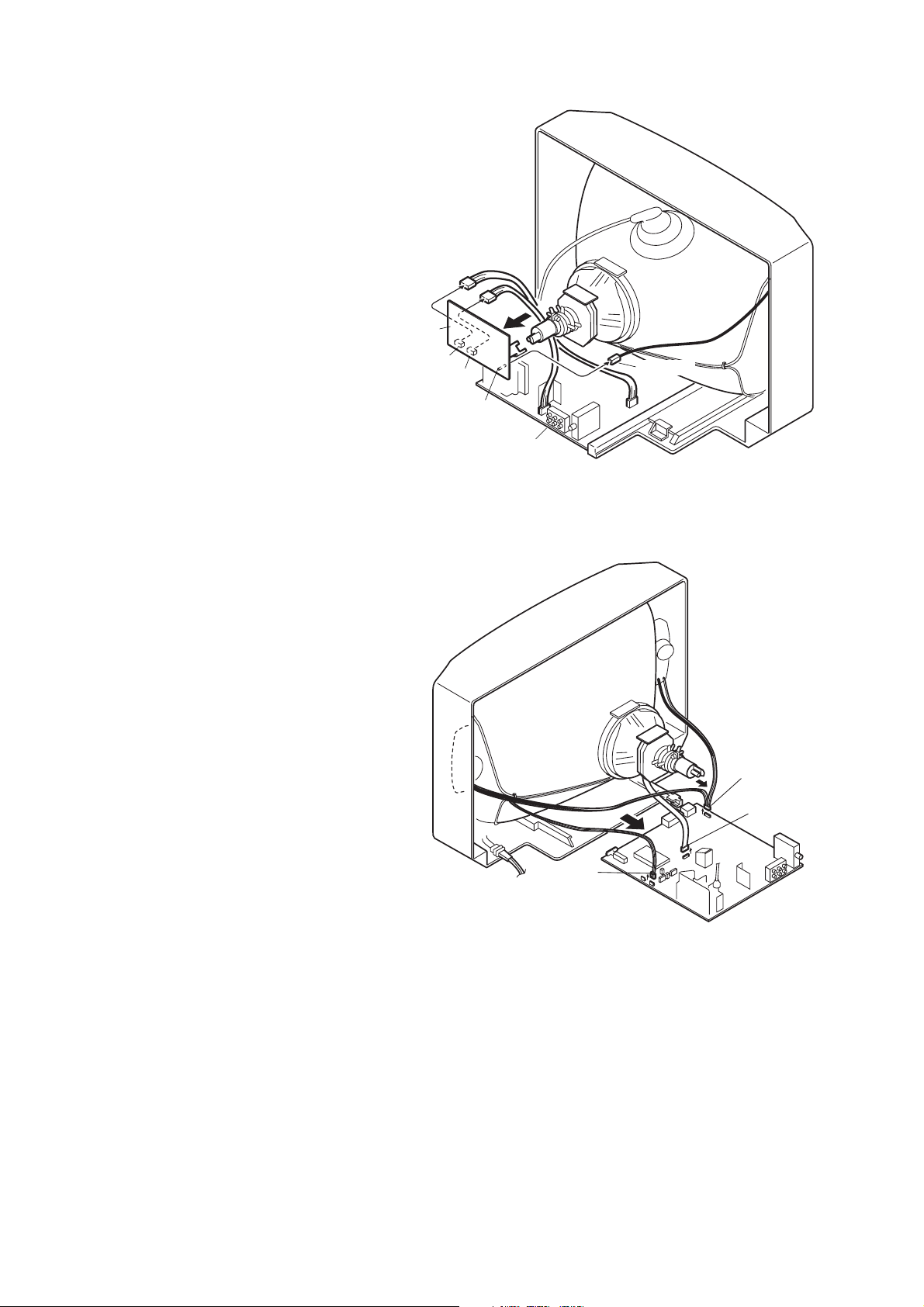
4. NK C.B REMOVAL
(1) Disconnect CN903 (CRT GND).
(2) Disconnect CN901, CN902.
(3) Pul out the NK C.B. in the direction of arrow.
(See Figure 4)
BT301
BT601
NK C.B
5. MAIN C.B REMOVAL
(1) Disconnect CNA401, CN601 and CN802.
(2) Pull out the Main C.B. in the direction of the arrow.
(See Figure 5)
CN902
CN901
CRT GND
CN903
MAIN C.B
Figure 4
CNA401
CN601
CN802
Figure 5
8
Page 9

ELECTRICAL MAIN PARTS LIST
REF. NO PART NO. KANRI DESCRIPTION
IC
87-A20-364-010 IC,KIA7809PI
87-027-666-010 IC,TC4052BP
87-A20-312-010 IC,M62420SP
87-070-237-010 IC,LA7832
87-A30-041-110 TR,SE115N
87-A20-611-080 IC,M51943BSL-700A
8Z-JAD-621-010 IC,M37272M8-165SP
87-A91-538-010 RCR UNIT,SBX1981-72P
87-A21-433-010 IC,KS24C041I
87-A21-299-010 IC,LA6458SLL
8Z-JBJ-605-010 IC,TA1268N
87-002-421-010 IC,NJM2233BL
87-A21-283-010 IC,AN5277
87-A21-259-010 IC,MM1454XD
87-A21-169-010 IC,MM1124B
87-A21-345-010 IC,NJM2150
87-A21-344-010 IC,STR-F6656
TRANSISTOR
89-337-794-580 TR,2SC3779 D/E
87-A30-091-080 FET,2SJ460
87-A30-114-080 TR,2SD1207T
89-208-922-380 TR,2SB892 ST
87-026-269-080 TR,DTA114ES
89-327-854-080 TR,2SC2785F
89-111-755-080 TR,2SA1175F
87-A30-121-080 TR,DTC 323 TS
87-A30-090-080 FET,2SK2541
87-A30-176-010 TR,2SC1573A P/Q/R
89-320-012-080 TR,2SC2001L
87-A30-095-010 TR,2SD2333LS/C202
DIODE
87-017-654-060 DIODE,GBU6JL6131
87-070-111-060 DIODE,RU30A
87-017-352-090 DIODE,RU3YX
87-070-112-060 DIODE,RU4YX
87-017-931-080 ZENER,MTZJ5.6B
87-002-743-080 ZENER,MTZJ 33B
87-070-136-080 ZENER,MTZJ5.1B
87-A40-523-080 ZENER,MTZJ9.1B
87-A40-348-080 ZENER,MTZJ3.3A
87-020-465-080 DIODE,1SS133 (110MA)
87-A40-286-080 DIODE,RGP10JE-5025
87-070-274-080 DIODE,1N4003 SEM
87-017-932-080 ZENER,MTZJ6.2B
87-A40-450-090 DIODE,RU 1P
87-A40-611-080 ZENER,MTZJ3.9B
87-A40-249-080 ZENER,MTZJ 15A
MAIN C.B
BT301 87-JBC-625-010 CONN ASSY,5P V WHT TV-NK
BT401 8Z-JAE-615-110 CONN ASSY,4P V GRAY JK
BT601 87-JBC-626-010 CONN ASSY,4P V WHT TV-NK
C1 87-016-624-080 CAP,E 10-16 SSL
C2 87-018-134-080 CAPACITOR,TC-U 0.01-16
C3 87-018-134-080 CAPACITOR,TC-U 0.01-16
C5 87-016-633-080 CAP,E 1-50 SSL
C6 87-018-134-080 CAPACITOR,TC-U 0.01-16
C7 87-016-621-080 CAP,E 220-10 SSL
C10 87-018-119-080 CAP, CER 100P-50V
C15 87-018-123-080 CAP, CER 220P-50V
C16 87-016-633-080 CAP,E 1-50 SSL
C17 87-018-131-080 CAP, CER 1000P-50V
C18 87-018-128-080 CAP, CERA-SOL SS 560P
NO.
REF. NO PART NO. KANRI DESCRIPTION
C19 87-016-629-080 CAP,E 0.1-50 SSL
C21 87-018-115-080 CAP, CER 47P-50V
C22 87-018-115-080 CAP, CER 47P-50V
C23 87-018-125-080 CAP, CER 330P-50V
C24 87-018-131-080 CAP, CER 1000P-50V
C25 87-016-629-080 CAP,E 0.1-50 SSL
C28 87-018-117-080 CAP,TC-U 68P-50 SL
C29 87-018-117-080 CAP,TC-U 68P-50 SL
C101 87-016-636-080 CAP,E 4.7-50 SSL
C104 87-016-621-080 CAP,E 220-10 SSL
C106 87-A10-576-010 CAP,CER 0.01-50 Z YF
C110 87-018-134-080 CAPACITOR,TC-U 0.01-16
C111 87-018-134-080 CAPACITOR,TC-U 0.01-16
C201 87-018-134-080 CAPACITOR,TC-U 0.01-16
C202 87-018-134-080 CAPACITOR,TC-U 0.01-16
C203 87-016-632-080 CAP,E 0.47-50 SSL
C204 87-018-134-080 CAPACITOR,TC-U 0.01-16
C205 87-016-577-080 CAP,E 470-16 SSL
C207 87-016-632-080 CAP,E 0.47-50 SSL
C208 87-018-134-080 CAPACITOR,TC-U 0.01-16
C209 87-016-576-080 CAP,E 330-16 SSL
C210 87-018-115-080 CAP, CER 47P-50V
C211 87-A11-080-080 CAP,TC U 47P-50 J CH
C214 87-016-627-080 CAP,E 47-16 SSL
C251 87-018-134-080 CAPACITOR,TC-U 0.01-16
C252 87-016-574-080 CAP,E 100-16 SSL
C253 87-A10-112-080 CAP,E 100-10 SSL
C254 87-015-464-080 CAP,E 4.7-16 BP
C255 87-015-464-080 CAP,E 4.7-16 BP
C301 87-016-624-080 CAP,E 10-16 SSL
C302 87-016-624-080 CAP,E 10-16 SSL
C303 87-016-624-080 CAP,E 10-16 SSL
C304 87-016-637-080 CAP,E 10-50 SSL
C305 87-018-134-080 CAPACITOR,TC-U 0.01-16
C306 87-016-574-080 CAP,E 100-16 SSL
C308 87-016-632-080 CAP,E 0.47-50 SSL
C310 87-018-119-080 CAP, CER 100P-50V
C311 87-A11-148-080 CAP,TC U 0.1-50 Z F
C312 87-A11-148-080 CAP,TC U 0.1-50 Z F
C313 87-A11-148-080 CAP,TC U 0.1-50 Z F
C314 87-018-134-080 CAPACITOR,TC-U 0.01-16
C315 87-018-131-080 CAP, CER 1000P-50V
C316 87-016-634-080 CAP,E 2.2-50 SSL
C317 87-016-634-080 CAP,E 2.2-50 SSL
C318 87-018-134-080 CAPACITOR,TC-U 0.01-16
C319 87-016-575-080 CAP,E 220-16 SSL
C320 87-016-587-090 CAP,E 1000-25 M SSL
C321 87-016-636-080 CAP,E 4.7-50 SSL
C323 87-016-625-080 CAP,E 22-16 SSL
C324 87-016-632-080 CAP,E 0.47-50 SSL
C328 87-016-624-080 CAP,E 10-16 SSL
C330 87-016-633-080 CAP,E 1-50 SSL
C332 87-018-134-080 CAPACITOR,TC-U 0.01-16
C333 87-018-125-080 CAP, CER 330P-50V
C334 87-018-134-080 CAPACITOR,TC-U 0.01-16
C335 87-016-574-080 CAP,E 100-16 SSL
C336 87-A11-148-080 CAP,TC U 0.1-50 Z F
C338 87-016-632-080 CAP,E 0.47-50 SSL
C342 87-010-529-080 CAP,E 1-50 BP
C343 87-018-131-080 CAP, CER 1000P-50V
C344 87-A11-080-080 CAP,TC U 47P-50 J CH
C346 87-016-622-080 CAP,E 470-10 SSL
C348 87-018-126-080 CAP,TC-U 390P-50 B
C401 87-018-134-080 CAPACITOR,TC-U 0.01-16
C402 87-016-627-080 CAP,E 47-16 SSL
!C403 87-010-399-090 CAP,E 3300-35 SME
C404 87-018-134-080 CAPACITOR,TC-U 0.01-16
C405 87-018-134-080 CAPACITOR,TC-U 0.01-16
C406 87-018-134-080 CAPACITOR,TC-U 0.01-16
C407 87-016-627-080 CAP,E 47-16 SSL
NO.
9
Page 10

REF. NO PART NO. KANRI DESCRIPTION
C408 87-016-574-080 CAP,E 100-16 SSL
C409 87-016-625-080 CAP,E 22-16 SSL
C410 87-016-624-080 CAP,E 10-16 SSL
C411 87-016-624-080 CAP,E 10-16 SSL
C412 87-016-624-080 CAP,E 10-16 SSL
C413 87-016-624-080 CAP,E 10-16 SSL
C414 87-016-624-080 CAP,E 10-16 SSL
C415 87-016-633-080 CAP,E 1-50 SSL
C416 87-016-633-080 CAP,E 1-50 SSL
C417 87-018-134-080 CAPACITOR,TC-U 0.01-16
C418 87-016-624-080 CAP,E 10-16 SSL
C419 87-A10-112-080 CAP,E 100-10 SSL
C428 87-016-627-080 CAP,E 47-16 SSL
C429 87-016-627-080 CAP,E 47-16 SSL
C430 87-018-134-080 CAPACITOR,TC-U 0.01-16
C435 87-016-627-080 CAP,E 47-16 SSL
C436 87-018-134-080 CAPACITOR,TC-U 0.01-16
C437 87-016-624-080 CAP,E 10-16 SSL
C440 87-016-627-080 CAP,E 47-16 SSL
C444 87-016-633-080 CAP,E 1-50 SSL
C445 87-016-591-080 CAP,E 100-35 SSL
C447 87-016-633-080 CAP,E 1-50 SSL
C449 87-016-588-090 CAP,E 2200-25 SSL
C450 87-016-588-090 CAP,E 2200-25 SSL
C453 87-016-574-080 CAP,E 100-16 SSL
C454 87-016-624-080 CAP,E 10-16 SSL
C455 87-016-624-080 CAP,E 10-16 SSL
C459 87-015-464-080 CAP,E 4.7-16 BP
C460 87-015-464-080 CAP,E 4.7-16 BP
C465 87-018-134-080 CAPACITOR,TC-U 0.01-16
C466 87-016-624-080 CAP,E 10-16 SSL
C473 87-018-118-080 CAP,TC-U 82P-50 B
C474 87-018-118-080 CAP,TC-U 82P-50 B
C475 87-018-117-080 CAP,TC-U 68P-50 SL
C476 87-018-117-080 CAP,TC-U 68P-50 SL
C477 87-015-464-080 CAP,E 4.7-16 BP
C478 87-015-464-080 CAP,E 4.7-16 BP
C487 87-016-633-080 CAP,E 1-50 SSL
C488 87-016-633-080 CAP,E 1-50 SSL
C495 87-018-115-080 CAP, CER 47P-50V
C496 87-018-115-080 CAP, CER 47P-50V
C502 87-A10-831-080 CAP,E 1000-25 M SMG
C503 87-016-633-080 CAP,E 1-50 SSL
C504 87-016-633-080 CAP,E 1-50 SSL
C508 87-A10-469-080 CAP,CER 2200P-500 K B DD10
C510 87-018-131-080 CAP, CER 1000P-50V
C511 87-016-591-080 CAP,E 100-35 SSL
C601 87-016-644-080 CAP,E 10-100 SSL
C604 87-016-593-080 CAP,E 470-35 M SSL
C606 87-A10-675-090 CAP,M/P 0.56-250 J
C608 87-A10-833-010 CAP,CER 1000P-2K K R LONG
C609 87-A11-047-090 CAP,M/P 8200P-1.25 H PHS
!C610 87-010-974-080 CAP,CER 220P-500 B
!C611 87-010-974-080 CAP,CER 220P-500 B
C612 87-016-624-080 CAP,E 10-16 SSL
C615 87-016-215-080 CAP,E 1-160 M TWSS
C616 87-A10-833-010 CAP,CER 1000P-2K K R LONG
!C801 87-A10-688-090 CAP,M/P 0.22-275 K (B81133)
!C803 87-A10-517-010 CAP,CER 3300P-4K M E KX
!C804 87-A10-517-010 CAP,CER 3300P-4K M E KX
C805 87-016-633-080 CAP,E 1-50 SSL
C806 87-A11-825-010 CAP,CER 120P-2K J SL
C807 87-018-127-080 CAP, CER 470P-50V
!C808 87-A11-992-090 CAP,E 330-400 105 KMH
C810 87-016-628-080 CAP,E 10-25 SSL
C811 87-016-582-080 CAP,E 47-25 SSL
C812 87-A11-302-090 CAP,M/P 0.01-630 J ECQF6(ZH)
C814 87-018-130-080 CAP,TC-U 820P-50 B
C815 87-A10-860-090 CAP,CER 470P-2K K R
C816 87-A10-731-090 CAP,E 220-160 M KMF
NO.
REF. NO PART NO. KANRI DESCRIPTION
!C817 87-A10-688-090 CAP,M/P 0.22-275 K (B81133)
C819 87-016-587-090 CAP,E 1000-25 M SSL
C821 87-010-446-010 CAP,E 2200-35 KME
C822 87-016-515-010 CAP,CER 1000P-1K KB
C827 87-016-587-090 CAP,E 1000-25 M SSL
C830 87-A11-824-010 CAP,CER 100P-2K J SL
C831 87-A10-858-090 CAP,CER 330P-2K KR
CF201 84-LB3-626-010 FLTR,TPS4.5MB2
CF202 87-008-574-080 FLTR,SFSH4.5MCB
CN1 87-009-195-010 CONN,5P B5BEH
CN401 87-049-469-010 CONN,4P V
CN601 87-A60-933-010 CONN,4P V B04(5-3)B-DVS-L
CN604 87-A60-485-010 CONN,2P V LV GRA
!CN801 87-099-674-010 CONN,2P VA V
!CN802 82-481-649-010 PLUG,2P MINI(*)
CNA401 87-JB8-601-010 CONN ASSY,4P SP-20
D1 87-070-110-010 LED,SLP-181B-51
D810 87-A90-965-010 VRIS,TNR15G471K
!F801 87-035-192-010 FUSE, 4AT
FB801 87-003-320-080 F-BEAD,FBR07HA121NB
FB803 87-003-320-080 F-BEAD,FBR07HA121NB
FB804 87-003-320-080 F-BEAD,FBR07HA121NB
FB805 87-003-320-080 F-BEAD,FBR07HA121NB
FB806 87-003-320-080 F-BEAD,FBR07HA121NB
FB807 87-003-320-080 F-BEAD,FBR07HA121NB
!FC801 87-033-213-080 CLAMP, FUSE
!FC802 87-033-213-080 CLAMP, FUSE
FR601 87-A00-063-060 RES,FUSE 2.2-1/2W J R-TYPE
FR602 87-A00-055-060 RES,FUSE 2.2-2WJ R-TYPE
FR604 87-A00-106-060 RES,FUSE 3.3-1W J R-TYPE
FR801 87-029-070-090 RESISTOR, FUSE 1/4W 2.2
HL1 84-LB3-216-010 HLDR,LED
J401 87-A60-856-010 JACK,PIN 3P
J402 87-A60-324-110 JACK,PIN 6P Y-W-R W/SW
J403 87-A60-858-010 JACK,3.5 BLK ST 2 SW
L2 87-005-614-080 COIL 100UH LAV35 J
L104 87-003-139-080 COIL,0.56UH
L201 8Z-JBR-612-010 COIL,SIF 4.5MHZ 504BN
L203 87-003-148-080 COIL BIAS 33UH
L204 87-003-282-080 COIL,12UH
L205 8Z-JBH-610-010 COIL,PIF-SQ57EL349A 45.75MHZ
L206 87-005-612-080 COIL,68UH J LAV35
L207 87-003-147-080 COIL, 22UH
L208 87-003-150-080 COIL, 68UH J LAL02
L251 87-005-610-080 COIL,47UH LAV35 J
L401 87-005-507-080 COIL,22UH FL0606 J
L402 87-005-507-080 COIL,22UH FL0606 J
L403 87-005-610-080 COIL,47UH LAV35 J
L404 87-005-507-080 COIL,22UH FL0606 J
L602 87-A50-040-010 COIL,2.2MH
L801 87-A50-176-080 COIL,33UH-PJ87
!LF801 87-JB8-651-010 FLTR,LINE SS24H-K15070
!LF802 8Z-JAD-610-010 FLTR,LINE FLF 15N022AV
!PR801 87-A90-090-080 PROTECTOR,1.5A 491SERIES 60V
!PR802 87-A90-195-080 PROTECTOR 7A 60V 491SERIES
!PR804 87-A90-195-080 PROTECTOR 7A 60V 491SERIES
!PS801 87-A91-407-010 P-COUPLER,ON3171-R
!PS802 87-A91-407-010 P-COUPLER,ON3171-R
!PT801 8Z-JAD-801-010 PT,SW ZJA-D
R107 87-A00-154-090 RES,M/F 18K-1W J RSF(S)
R110 87-A00-160-090 RES,M/F 33-2W J RSF(S)
R312 87-025-602-090 RES,M/O 39-2W J
R429 87-025-381-080 RES,M/F 18K-1/6W F
R430 87-025-424-080 RES,M/F 10K 1/6W F
R431 87-025-380-080 RES,M/F 15K-1/6W F
R432 87-025-381-080 RES,M/F 18K-1/6W F
R450 87-A00-624-090 RES,M/F 3.3-7W J RSV7
R505 87-A00-563-090 RES,M/F 1.5-1/2W J ERXS
R606 87-A00-196-090 RES,M/F 0.47-1/2W J RSF(S)
NO.
10
Page 11
TRANSISTOR ILLUSTRATION
REF. NO PART NO. KANRI DESCRIPTION
R610 87-A00-123-090 RES,M/F 3.9K-2W J RSI-2S B
R611 87-A00-561-090 RES,M/F 4.7K-2W J ERGS
R624 87-A00-544-090 RES,M/F 220-3W J ERGS
R804 87-A00-543-080 RES,SD 8.2M-1W J RCR60
R806 87-A00-204-090 RES,CEM 0.18-5W K
R809 87-A00-552-010 RES,CEM 1.0-10W J MPC722
R810 87-A00-552-010 RES,CEM 1.0-10W J MPC722
R812 87-A00-576-090 RES,M/F 27K-5W J RSV5
R813 87-A00-577-090 RES,M/F 22K-2W J RSF(S)
R816 87-A00-411-090 RES,M/F 33K-1W J
R824 87-A00-577-090 RES,M/F 22K-2W J RSF(S)
SF201 8Z-JBH-633-010 FLTR,SAW M1969-US
SW2 87-A90-712-080 SW,TACT EVQ11L07K
SW3 87-A90-712-080 SW,TACT EVQ11L07K
SW4 87-A90-712-080 SW,TACT EVQ11L07K
SW5 87-A90-712-080 SW,TACT EVQ11L07K
SW6 87-A90-712-080 SW,TACT EVQ11L07K
SW7 87-A90-712-080 SW,TACT EVQ11L07K
!SW801 87-A90-364-010 SW,PUSH SDDLB1-C-D-2
!T601 8Z-JBS-605-010 FBT, HFT3608(SAN)20-C
!T602 8Z-JBH-615-010 TRANS,US ETH09K10AZ
!TH801 87-A91-405-010 POS-THMS,T209-B80-A10
TU101 8Z-JBE-610-010 TU UNIT,USA ENV56D74G3
X1 87-A70-124-080 VIB,CER 8.0MHZ
X301 87-A70-007-080 VIB,XTAL 3.58MHZ AQC-1001
X302 87-030-327-010 VIB,CER CSB503F30
NO.
REF. NO PART NO. KANRI DESCRIPTION
NK C.B
C901 87-012-372-010 CAP,CER 1000P-2K
C902 87-018-125-080 CAP, CER 330P-50V
C903 87-018-125-080 CAP, CER 330P-50V
C904 87-018-125-080 CAP, CER 330P-50V
!C905 87-010-976-080 CAP,CER 1000P-500 B
C907 87-016-577-080 CAP,E 470-16 SSL
C908 87-016-627-080 CAP,E 47-16 SSL
CN901 87-049-469-010 CONN,4P V
CN902 87-A60-622-010 CONN,5P V 2MM JMT
CN903 87-A60-485-010 CONN,2P V LV GRA
L901 87-005-615-080 COIL,120UH J LAV35
R904 87-A00-165-090 RES,M/F 15K-2W J RSF(S)
R905 87-A00-165-090 RES,M/F 15K-2W J RSF(S)
R906 87-A00-165-090 RES,M/F 15K-2W J RSF(S)
S901 86-LBU-670-010 SOCKET,CRT 9P CVT3326 1603
NO.
E C B E C B
2SB892
2SC1573
B E C
2SC3779
2SD1207
2SA1175
2SC2785
2SC2001
S D G
2SJ460
2SK2541
E C B
DTA114ES
DTC323TS
B C E
2SD2333
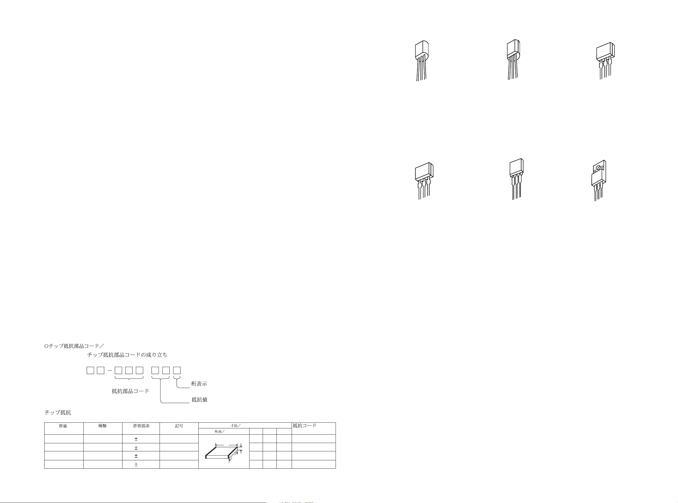
CHIP RESISTOR PART CODE
Chip Resistor Part Coding
88
A
Resistor Code
Chip resistor
Wattage Type Tolerance
1/16W 1005 5% CJ
1/16W
1/10W
1/8W
1608
2125
3216
5%
5%
5%
Symbol
CJ
CJ
CJ
Figure
Value of resistor
Form
L
Dimensions (mm)
t
W
0.55
Resistor Code
108
118
128
LW t
1.0 0.5 0.35 104
1.6 0.8 0.45
2 1.25 0.45
3.2
1.6
: A
: A
1211
Page 12

SCHEMATIC DIAGRAM-1 (MAIN SECTION)
TP102
TP202
TP302
1413
Page 13

WIRING-1 (MAIN C.B SECTION)
1
A
B
C
D
234567
8
9
10
11 12 13
14
E
F
G
H
I
J
1615
Page 14

SCHEMATIC DIAGRAM-2 (NK SECTION)
WIRING-2 (NK C.B SECTION)
1
A
B
C
D
23456
7
E
F
G
H
I
J
1817
Page 15

WAVEFORM
IC1 Pin 17 (CV IN)
1
IC301 Pin 21 (B OUT)
5
1
IC1 Pin 20 (XOUT)
2
2
IC301 Pin 19 (R OUT)
3
500 mV/div
20 µs/div
1 V/div
50 ns/div
5
IC301 Pin 30 (FBP IN)
6
6
IC301 Pin 32 (H OUT)
7
1 V/div
20 µs/div
2 V/div
20 µs/div
3
IC301 Pin 20 (G OUT)
4
4
1 V/div
20 µs/div
1 V/div
20 µs/div
7
IC301 Pin 34 (32FH VCO)
8
8
1 V/div
20 µs/div
50 mV/div
500 ns/div
19
Page 16

IC301 Pin 43 (Y IN)
9
Between X301 & C309 (VCXO)
13
9
IC301 Pin 45 (CHROMA IN)
10
10
IC301 Pin 47 (TV DET OUT)
11
200 mV/div
20 µs/div
200 mV/div
20 µs/div
13
IC501 Pin 2 (V-OUT)
14
14
Q601 Collector
15
50 mV/div
100 ns/div
10 V/div
5 ms/div
11
IC301 Pin 54 (DE EMPHASIS)
12
12
500 mV/div
20 µs/div
200 mV/div
1 ms/div
15
Q602 Collector
16
16
200 V/div
20 µs/div
50 V/div
20 µs/div
20
Page 17

T601 Pin 8 (E24)
17
Q902 Collector (G) --- NK C.B
19
17
Q901 Collector (R) --- NK C.B
18
18
50 V/div
20 µs/div
20 V/div
20 µs/div
19
Q903 Collector (B) --- NK C.B
20
20
20 V/div
20 µs/div
20 V/div
20 µs/div
21
Page 18

IC DESCRIPTION
IC, M37272M8-165SP
Pin No. Pin Name I/O Description
1 HD I OSD horizontal synchronised signal input terminal. "L"= active.
2 VD I OSD vertical synchronised signal input terminal. "L"= active.
3 A MUTE
4 L MUTE
5 A DET OUT O Not used.
6 SW/SBASS O SBASS ON "L", OFF "H".
7 SEL1 O
8 SEL2 O
9 SP MUTE O Used to mute the speaker (sound) output.
10 REMOCON I Remote control signal is led to this pin.
O Used to mute line out sound and picture when no input signal is detected. "H" to mute.
Selecting tuner receiving band.
Pin 7 Pin 8
TUNER L L Reset start : Both of Pin 7, Pin 8 are "H".
VIDEO 1 L H
VIDEO 2 H L
11 SD I
12 EXT I I
13 PON O
Horizontal sync. detected input. The level of this pin will be sampled by µ-P to
determine whether there is picture signal detected.
2
C switching.
During standby mode, "H" level is inserted to switch off horizontal deflection and high
voltage.
14 A VCC – 5V supply.
15 HLF – Connected to filter.
16 V HOLD – Connected to condensor.
17 CV IN I Video signal input.
18 CNVSS – Connected to ground.
19 XIN I 8 MHz clock input.
20 XOUT O 8 MHz clock output.
21 VSS – Connected to ground.
22 VCC – 5 V supply.
23 BBE 1 O
Pin 23 Pin 24
OFF L L
LOW H L
24 BBE 2 O
HIGH H H
25 RST I Used to reset the µ-P when power up.
26 D DET A I Connected to ground through a resistor.
27 D DET F
I Fault detection. Detect as a fault when the voltage is more than 2.5V.
28 D DET R
29 AFTV I AFT voltage from IC301 is received by µ-P during channel tuning.
30 KEY I Input key is detected by monitor.
31 SDA2 I/O I
32 SDA1 I/O I
33 SCL2 I/O I
2
C bus CH2 data.
2
C bus CH1 data.
2
C bus CH2 clock.
34 SCL1 I/O I2C bus CH1 clock.
22
Page 19

Pin No. Pin Name I/O Description
35 S OUT O Not used.
36 QSUR O Surround ON "H", OFF "L".
37 LED O LED ON "L", OFF "H".
38 WP O E
2
PROM write protect.
39 FAST BLK O OSD blanking output.
40 B O OSD blue output.
41 G O OSD green output.
42 R O OSD red output.
IC, TA1268N
Pin No. Pin Name I/O Description
1 NC – Not connected.
2 AUDIO OUT O
Sound output. The maximum flew out current is 3.6mA.
So, the minimum load resistor is 1kΩ. (Not used)
3 RF AGC O RF AGC output.
4 SIF TANK – Tank coil connection for SIF detection circuit.
5 AGC FILT – PIF 2nd AGC filter.
6 PIF GND – GND for PIF circuit.
7 ~ 8 PIF IN I IF input. The typical input value is 90dBµV.
9 PIF VCC – VCC for PIF circuit.
10 LOOP FILT – PIF PLL loop filter.
11 APC FILT – APC filter of fsc oscillation.
12 VCXO I X'tal of 3.58MHz VCXO.
13 GND – V/C/D GND.
14 FAST BLANKING I Fast blanking of RGB input.
15 R IN I R signal input.
16 G IN I G signal input.
17 B IN I B signal input.
18 D VCC – VCC for digital circuit.
19 R OUT O R primary color signal output.
20 G OUT O G primary color signal output.
21 B OUT O B primary color signal output.
22 V OUT O Vertical pulse output.
23 NFB I NFB input.
24 V RAMP O Vertical ramp output.
25 V SEPA FILT – Vertical sync. separation filter.
26 H VCC – VCC for horizontal circuit.
23
Page 20

Pin No. Pin Name I/O Description
27 ~ 28 SCL, SDA I/O Input and output of I
Inputting of X-RAY protect circuit. The threshold voltage is 3.5V (typ.).
29 X RAY I If the voltage that is applied is more than the threshold voltage, the X-RAY
protect circuit make horizontal output a low.
2
C Bus.
30 FBP IN I
Fly-back pulse input. The Fly-back pulse is the reference of AFC circuit, gate pulse
and so on. The current needs to keep under 1mA.
31 SYNC OUT O Sync. pulse output.
32 H OUT O Horizontal pulse output.
33 H AFC –
Horizontal AFC filter. The AFC circuit fits the phase between inputted horizontal
sync. signal and horizontal pulse which is made by countdowning 32fH.
34 32FH VCO – Ceramic oscillator connection. That constitutes 32fH (503kHz) oscillation circuit.
35 D GND – GND for digital circuit.
36 ABL O ABL circuit.
37 TV IN I Inputting of PIF detected signal. The typical input amplitude is 1.0Vp-p.
38 ACL O ACL circuit.
39 EXT VIDEO I Inputting of external video signal.
40 BLANK DET – Filtering of black peak detection.
41 AV SW OUT O
Video switch output which selects TV signal or external video.
Amp gain: Min. 1.7, Typ. 1.9, Max. 2.1.
42 DC REST I Filtering of APL detection.
43 Y IN I Y signal input. The typical input amplitude is 1.0Vp-p.
AFT output. Monitor signal output can be selected via Bus.
B0 B1 OUTPUT
44 AFT O
0 0 AFT
0 1 TEST purpose only
10B
1 1 (RF AGC)/2
45 CHROMA IN I
Chrominance signal input. The typical input signal amplitude is 286mVp-p (at burst
signal). This IC will go to test mode when this terminal voltage is higher than 4.5V.
46 VCC – VCC for video, chroma and deflection circuit.
47 TV DET OUT O PIF detected signal output.
48 SIF VCC – VCC for SIF circuit.
49 ~ 50 PIF TANK – Tank coil connection for PIF detection circuit.
51 SIF GND – GND for SIF circuit.
52 LIMIT IN I Inputting of SIF limiter amplifier circuit.
53 AUDIO TV IN I Inputting of SIF detected signal. (Not used)
54 DE-EMPHASIS O Filtering of SIF de-emphasis.
55 EXT AUDIO IN I External audio input. (Not used)
56 NC – Not connected.
24
Page 21

IC BLOCK DIAGRAM
IC, MM1454XD
VCC
LIN
VREF
QF1
QF2
QF3
16 15 14 13 12 11 10 9
QSURROUND
BIAS
QF4
QF5
87654321
IC, TA1268N
RIN
PNR
B/Q
BET
QF6
ROUT
LOUT
GND
IC, SBX1981-72P IC, M51943BSL-700A
25
Page 22

IC, KS24C041I
IC, TC4052BP IC, M62420SP
IC, STR-F6656
26
Page 23

IC, MM1124B IC, NJM2233BL
1234567
GND
POMP UP
VERTICAL
DRIVE
VERTICAL
OUTPUT
THERMAL
PROTECT
V-OUT
PS
V-OUT
INPUT
OSC STEP
VCC
PULSE
GND
IC, NJM2150
IC, AN5277
IC, LA7832
27
Page 24

SET-UP FOR ADJUSTMENT
B
G
R
R/B
G
Because the video signal output from a pattern generator is used as
the adjustment signal input during adjustment, the video signal
output from the pattern generator must conform with the
specifications. Measure the output waveform across 75 Ω load.
Confirm that the synchronizing signal has an amplitude of about
0.3 V, the video signal portion has an amplitude of about 0.7 V and
the burst signal has an amplitude of about 0.3 V with flat envelope.
Confirm that ratio of the burst signal amplitude and the red signal
amplitude is 0.30 : 0.66. If the output signal does not conform with
the specifications, calibrate the pattern generator. (Refer to pattern
generator operation manual.)
Use the LEADER: LCG 404 for the pattern generator.
1. CRT ADJUSTMENT
1-1. Precautions
(1) Receive the white raster signal, and then perform aging for at
least 20 minutes.
(2) Demagnetize the area surronding the CRT with a degausser
before making adjustments.
(3) Set the picture quality for each mode to the factory setting.
(4) Position the front screen facing the east as much as possible.
1-2. Purpose
(1) Beam landing adjustment (purity magnet)
Set the left/right balance of beam landing. If there is a
discrepancy in this adjustment, a color irregularity will occur.
After completion of the landing adjustment, it is necessary to
perform convergence adjustment.
Approx. 0.7V
1 Vp-p
White (Approx.
Burst signal
75%)
Approx.
Approx. 0.3V
Cyan
Yellow
75% white
Green
Red
Magenta
Blue
Black
0.3V
TV display
Color bar signal of a pattern generator
Precautions before starting adjustment
Satisfy the following setting conditions before starting adjustment.
• Allow warm-up of 20 minutes or longer. (Do not turn off during
warm-up.)
• Set all picture quality controls of users' setting to initial set-up,
unless otherwise specified.
• Picture quality reset
1. Select "Picture" on the screen menu and press enter button.
2. Select "Normal" and press enter button.
3. Select "Reset" and press enter button.
• Set the pattern generator’s output level to 1.0Vp-p (across 75Ω
load).
Before adjustment
Color
irregularity
After adjustment
Fig. 1-1
(2) Beam convergence adjustment (4-pole magnet)
Align the R beam with the B beam. The G beam does not
move with this adjustment.
(magenta)
Align the R beam with the B beam
Fig. 1-2
(3) Beam convergence adjustment (6-pole magnet)
With a 4-pole magnet align the G beam with the already aligned
R/B beam.
(magenta)
R/B
G
(white)
RGB
Align the G beam with the R/B beam
Fig. 1-3
28
Page 25

(4) The composition of each magnet is as shown in Fig. 1-4.
SN NS
NS SN
NN
SS
SS
NN
In making adjustments, rotate the lock ring clockwise (looking
from the CRT’s back screen) and disengage.
Be careful not to loose the lock ring too much. If the magnet
assembly has become shifted during adjustments, secure it to
the position in Fig. 1-4.
DY lock screw
Purity 4-pole 6-pole
CRT DY
Magnet assembly
1-3.Beam Landing Adjustment
(1) Receive the green raster signal from the pattern generator.
(2) Loosen the magnet lock screw, and shift the magnet assembly
backward (toward the neck).
(3) Loosen the DY lock screw, and shift the DY deflecting yoke
backward (toward the neck).
(4) After opening the two purity magnets to the same angle, adjust
the color width of the bands on both sides of the screen so that
they are equal. (refer to Fig. 1-5 (a)).
Lock ring
Magnet assembly
lock screw
Fig 1-4
(5) Gradually shift the deflecting yoke toward the front (toward
the CRT funnel). Stop movement at the point when the screen
has become completely green.
NK C.B
RGB
As shown in Fig. 1-5 (b), the purity magnet functions in relation
to the electron beam.
Fig 1-5 (a)
R=B
Fig 1-5 (b)
(6) Also, verify the respective monochromatics of red and blue.
(7) While looking at the screen, adjust the tilt of the deflecting
yoke and tighten the DY lock screw.
(8) Shift the magnet assembly to the front (toward the CRT funnel),
stop movement before the adjustment position and then tighten
the magnet lock screw.
At this time, be careful not to shift the position of the purity
magnet.
29
Page 26

As there is occurrence of convergence distortion after
GRB
N
N
N
S
S
S
S
N
N
S
GRB
S
N
completing the landing adjustments, be sure to carry out
convergence adjustments.
If the color irregularities in the screen’s corner section are
not improved, correct them with the landing magnet. After
using the landing magnet, be sure to demagnetize the CRT
with degausser and verify that there is no occurrence of color
irregularity. (refer to Fig. 1-6)
Landing magnet: 81-JTI-710-010
(two-sided adhesive tape) : 80-XVI-218-010 Cushion
Landing magnet
Cushion
Since the landing magnet is polarized,
check the screen’s improvement through
rotation, not only by position.
Fig 1-6
1-4. Beam Center Convergence Adjustment
Make adjustments on the convergence with 4-pole and 6-pole
magnets. Operate each magnet in relation to the electron beam
as shown in Figs. 1-7 and 1-8. When performing this
adjustment, verify whether there is distortion in the focus
adjustment. If necessary, carry out adjustments again.
In Fig. 1-7, two 4-pole magnets are stacked together so as to be of
the same polarity. Move the B and R beams to their respective
direction, by rotating the two 4-pole magnets together. By adjusting
the opening of the two magnets, it is possible to adjust the amount
of the beam’s movement.
Fig 1-8
In Fig. 1-8, the two 6-pole magnets are stacked together so as to be
of the same polarity. Move the B and R beams to their respective
direction, by rotating the two 6-pole magnets together. By adjusting
the opening of the two magnets, it is possible to adjust the amount
of the beam’s movement.
(1) Receive the dot pattern signal from the pattern generator.
(2) Pay attention to the center of the screen, and perform
adjustments with two 4-pole magnets so that the R beam and
B beam are perfectly aligned and become a magenta color.
(Refer to Fig. 1-2)
(3) In the same way, pay attention to the screen, and perform
adjustments with a 6-pole magnet so that the magenta beam
and G beam are aligned and become a white dot.
(Refer to Fig. 1-3)
(4) After adjustments are completed, secure all magnets with the
lock link. (Refer to Fig. 1-4)
1-5.The Surrounding Convergence Adjustment
Perform this adjustment after completion of adjustment 1-4.
(1) Shake the deflecting yoke up, down to the right and left, and
adjust any discrepancies in the screen’s surroundings.
(2) Insert wedges in three locations in the gap between the
deflecting yoke and the surface of the CRT funnel in order
to secure the deflecting yoke. (Refer to Fig. 1-9)
SN
BGR
NS
S
BGR
NN
S
Wedge
Wedge
Wedge
Position of wedge
Fig 1-7
30
Fig. 1-9
Page 27

IC BUS Data Setting Procedure
AGING AFT OK 000H
0123456789ABC D E F
1100101111110 1 0 0
Fig. 1
Fig. 2
1 MONO
2 IN-ST
3 ST
4 ST+S
5 SPARE
With this model, most parts of video and deflection blocks can be
adjusted using a jig remote control.
Preparations:
• Modify the hidden keys on the RC-6VT06 jig remote control
(TV-C142/86-LB4-951-010) so that they can easily be pressed.
2 keys to be modified (see the figure below):
ON/OFF
FINISH key
(hidden key
under the seal)
TV/VIDEO
SLEEP
12
45
78109
SYSTEM
CHANNEL VOLUME
3
6
TEST key
(hidden key
under the seal)
SYSTEM key
Aging mode operation method: Be sure to
check this after replacing EEPROM.
1. Press the TEST key on the remote control to set to the aging
mode. See Fig. 1.
2. Press the SYSTEM key to check the status of distinction switch.
See Fig. 2.
• If the contents are different, press the "1" key to select "IN-ST"
for destination.
• To modify the data, use the channel keys to move the cursor to
0-F, and then use the volume keys to change it to "0" or "1".
Starting service mode:
Hidden key TEST:
• Pressing the TEST key on the jig remote control once will set the unit
to the aging mode. See Fig. 1.
• Pressing TEST again will set the unit to the adjustment mode.
Hidden key FINISH:
• Pressing the FINISH key on the jig remote control will reset the
accumulated hours in the aging mode.
• Do not press FINISH during normal servicing.
Contents of aging mode:
1. Releasing auto power off function
Release the auto power off function when no input is supplied.
Use this mode for warming up (aging) during CRT adjustment.
2. AFT S-curve status display
OK, UP or DN (down) will appear to show whether the AFT
S-curve status is optimum, too high or too low.
AFT S-curve
UP: Deviation from standard value high.
OK: Normal value
DN: Deviation from standard value low.
31
Page 28

3. CRT ON accumulated hour display
The CRT usage hours accumulate every hour, and are displayed
using hexadecimal number.
Example of calculating displayed hexadecimal number:
AFT OK 1234H IN-ST
1x163 + 2x162 + 3x161 + 4x160 = 4660 hours
4th digit 3rd digit 2nd digit 1st digit
* When the accumulated hours exceed 7FFFH (32,768 hours), the
display will be reset to 0000H.
Adjustment mode operation method:
1. Press the SYSTEM key to restore the aging display, and press
the TEST key again to display the adjustment menu.
PAGE 1
1 H POS
2 V POS
3 V SIZE
4 OSD POS
5 PIF VCO
6 RF AGC
PUSH
1~6 KEY
PAGE 1
1 H POS
2 V POS
3 V SIZE
4 OSD POS
SD
AFT
PUSH
CH UP/DN KEY
Adjustment menu chart
PUSH
CH UP/DN KEY
PAGE 2
00
00
00
00
00
00
1 R CUTOFF
2 G CUTOFF
3 B CUTOFF
4 G DRIVE
5 B DRIVE
ENTER CONTRAST
PUSH
1~5 KEY
Press MENU to return. Press MENU to return. Press MENU to return. Press MENU to return.
PAGE 2
0~31
5 PIF VCO
SD
AFT
6 RF AGC
0~7
0~63
0~48
OK
0~127
OK
0~63
1 R CUTOFF
2 G CUTOFF
3 B CUTOFF
4 G DRIVE
5 B DRIVE
PUSH
CH UP/DN KEY
0~255
0~255
PUSH
CH UP/DN KEY
00
00
00
00
00
0~255
0~255
0~255
PAGE 3
1 SUB CONTRAST
2 SUB BRIGHT
3 SUB TINT
4 SUB COLOR
PUSH
1~4 KEY
PAGE 3
1 SUB CONTR...
2 SUB BRIGHT
3 SUB TINT
4 SUB COLOR
PUSH
CH UP/DN KEY
00
00
00
00
-63~+63
-63~+63
-63~+63
PUSH
CH UP/DN KEY
PUSH
1~4 KEY
-63~+63
PAGE 4
1 358 TRAP
2 BPF
3 H AFC
4 WPL
PAGE 4
1 358 TRAP
2 BPF CUTOFF
3 H AFC
4 WPL
PUSH
CH UP/DN KEY
(Inoperable)
0: ON
1: OFF
2: AUTO
PUSH
CH UP/DN KEY
00
00
00
00
0: +2
1: +1
0: OFF
1: ON
Each value in the adjustment menu can be modified using the volume adjustment keys (+, -).
*
Pressing the audio muting key, etc. during menu screen operation will clear the menu contents: Press the "0" key to restore the menu.
*
Fig.3
32
Page 29

ELECTRICAL ADJUSTMENT (adjustment menu screen)
J403
J401
IC303
IC403
IC1
IC402
IC405
IC407
IC251
IC406
TP302
BT301
3
TP201
(AFT)
IC301
C322
T601
(FBT)
R211
TP202
FORCUS
L205
P-IF
TP203
C213
L201
S-IF
R101
TP102
(IF)
TU101
T601
(FBT)
TP101
(RF AGC)
J402
SFR
S901
R903
R902
TP902
R901
R906
R904
SCREEN
R905
33
Page 30

PAGE 1
3 V SIZE 5
13~14
squares
Fig.1-3
• After replacing EEPROM, enter the following initial values before
proceeding with adjustment.
• During normal servicing, check the applicable items, and adjust
them if necessary.
PAGE 1
1. H POS
2. V POS
3. V SIZE
4. OSD POS
5. PIF VCO
6. RF AGC
PAGE 2
1. R CUT OFF
2. G CUT OFF
3. B CUT OFF
4. G DRIVE
5. B DRIVE
PAGE 3
1. SUB CONTRAST
2. SUB BRIGHT
3. SUB TINT
4. SUB COLOR
PAGE 4
1. 3.58 TRAP
2. BPF
3. H AFC
4. WPL
Initial value
20
2
18
6
58
32
127
127
127
127
127
34
35
0
16
Specified value
ON
AUTO
+1
OFF
1-1. H POS Horizontal position adjustment/Adjustment menu
screen PAGE 1-1
Input signal: Crosshatch
Measuring instrument: Leader LCG-404 pattern generator
• Use the volume keys on the jig remote control to adjust so
that the dot mark at the center of crosshatch is positioned at
the horizontal center of screen and the squares on the left
and right are equal. Fig. 1-1
8~9 8~9
PAGE 1
1 H POS 18
Center
Fig.1-1
1-2. V POS Vertical position adjustment/Adjustment menu
screen PAGE 1-2
Input signal: Crosshatch
Measuring instrument: Leader LCG-404 pattern generator
• Use the volume keys on the jig remote control to adjust so
that the dot mark at the center of crosshatch is positioned at
the vertical center of screen. Fig. 1-2
1-3. V SIZE Vertical size adjustment/Adjustment menu screen
PAGE 1-3
Input signal: Crosshatch
Measuring instrument: Leader LCG-404 pattern generator
• Use the volume keys on the jig remote control to adjust so
that the number of crosshatch squares in the vertical direction
is 13-14. Fig. 1-3
1-4. OSD POS OSD position adjustment/Adjustment menu
PAGE 1-4
Input signal: Not specified
• Use the volume keys on the jig remote control to adjust so
that both sides of OSD characters are equal to the length of
edge of screen. A = B Fig. 1-4
PAGE 1
CRT center
mark
2 V POS 2
Fig.1-2
PAGE 1
OSD H 24
AB
Fig.1-4
34
Page 31

1 R CUTOFF
2 G CUTOFF
3 B CUTOFF
4 G DRIVE
5 B DRIVE
PAGE 2
127
127
127
127
127
Fig. 2-1
1-5. PIF VCO Video IF/VCO adjustment/Adjustment menu screen
PAGE 1-5
Input signal: ANT RF-INPUT
Color bar
• Measuring instruments: Leader LCG-404 pattern generator
Use the volume keys on the jig remote control to adjust so that
the AFT status on the screen is "OK". Fig. 1-5
• If there are several ranges where the AF status is acceptable,
select the center value.
* "NG" will appear for SD when no signal appears on the screen,
but this will not cause any problem for VCO adjustment
(example: No signal with video input). Even in this case,
adjustment is possible if there is a load on ANT.
White Balance Adjustment:
Adjustment menu screen PAGEs 2-1~5
* When the adjustment menu screen appears, the user picture
quality will be cleared.
Input signal: White raster
Details of adjustment: 1. R CUT OFF
2. G CUT OFF
3. B CUT OFF
4. G DRIVE
5. B DRIVE
* Perform aging for at least 20 minutes before adjustment.
* Repeat all processes of adjustment several times.
Measuring instrument: Leader LCG-404 pattern generator
Higher
OK
UP
58
Lower
OK
DN
52
PAGE 1
SD
AFT
5 PIF VCO
Optimum
OK
OK
58
Fig.1-5
1-6. RF AGC RF-AGC adjustment/Adjustment menu screen
PAGE 1-6
Input signal: ANT RF-INPUT
Color bar
Measuring instruments: Oscilloscope, Leader LCG-404 pattern
generator
1. Connect the oscilloscope to TP-101.
2. Use the volume keys on the jig remote control to adjust so
that the voltage at the test point is 3.5 ±0.3 V. Make sure
that "OK" appears for AFT on the adjustment menu screen
as shown in Fig. 1-6.
PAGE 1
Cutoff adjustment:
2-1. Use the pattern generator to input white raster signal.
2-2. Fix the cutoff value whose color seems to be most intense at
127, and use the volume keys on the jig remote control to adjust
the other two cutoff values so that a white picture appears.
Drive adjustment:
2-3. Use the volume keys on the jig remote control to increase the
4. G DRIVE value to 200 or more so that the picture is
greenish.
2-4. Decrease the value gradually until green disappears.
2-5. Use the volume keys on the jig remote control to increase the
5. B DRIVE value to 200 or more so that the picture is bluish.
2-6. Decrease the value gradually until blue disappears.
2-7. Perform steps 1-6 several times so that a white picture appears.
SD
AFT
6 RF AGC
Fig.1-6
OK
OK
32
Focus Adjustment:
Input signal: Dot signal
Adjustment point: Upper SFR of FBT (T601)
Measuring instrument: Leader LCG-404 pattern generator
• Adjust the upper SFR of FBT (T601) until the focus of dots in
the dot pattern is optimum.
35
Page 32

Screen Adjustment:
Fig. 3-3
One oblique line
Input signal: No signal (raster)
Adjustment point: Lower SFR of FBT (T601)
Measuring instrument: Leader LCG-404 pattern generator
1. Use the jig remote control to display the adjustment menu screen.
2. Press the "0" channel numeric key so that a horizontal single line
appears. Fig. 2-2
3. Adjust the lower SFR of FBT (T601) until the horizontal single
line starts to gleam.
4. Perform step (2) again to return to the adjustment menu screen.
3-3. SUB TINT Sub-tint adjustment/Adjustment menu screen
PAGE 3-3
Input signal: Color bar
VIDEO IN
Measuring instruments: Oscilloscope
Leader LCG-404 pattern generator
Test point: TP302/BT301 (wire connector) pin (3)
1. Connect the oscilloscope to TP302.
2. Use the volume keys on the jig remote control to adjust so
that the bottom edges of waveform are in one oblique line,
referring to Fig. 3-3.
Fig.2-2
3-1. SUB BRIGHT Sub-brightness adjustment / Adjustment menu
screen PAGE 3-2 (make sure of the order)
Input signal: Color bar (stairstep)
Measuring instrument: Leader LCG-404 pattern generator
1. Use the volume keys on the jig remote control to adjust until
the second step from the right gleams.
PAGE 3
3 SUB BRIGHT 37
2nd from right
Fig. 3-1
3-2. SUB CONTRAST Sub-brightness adjustment / Adjustment
menu screen PAGE 3-1
Input signal: Color bar (QIW) with chroma off
Measuring instruments: Oscilloscope
Leader LCG-404 pattern generator
Test point: TP902 on NK C.B.
1. Connect the oscilloscope to TP902.
2. Use the volume keys on the jig remote control to adjust so
that the voltage to the pedestal level from 100% white is
80 ± 2.0 V, referring to Fig. 3-2.
3-4. SUB COLOR Sub-color adjustment/Adjustment menu screen
PAGE 3-4
Input signal: Color bar
VIDEO IN
Measuring instruments: Oscilloscope
Leader LCG-401 pattern generator
Test point: TP302/BT301 (wire connector) pin (3)
1. Connect the oscilloscope to TP302.
2. Use the volume keys on the jig remote control to adjust so
that the peaks of waveform are in one straight line, referring
to Fig. 3-4.
Cyan
Horizontal straight line
Magenta
Fig. 3-4
1.0V
10 S
Pedestal level
80+2.0V
Fig. 3-2
75%white
100%white
36
Page 33

4. TV SETTING CHECK Settings check for different models/
1.0 V
0.5 ms
4.5 V
Fig.5-1
Adjustment menu screen PAGEs 4-1~4
The settings are fixed for each model: Do not change the
settings to those other than specified.
• Check to see if the settings on the adjustment menu screen
are the same as in Table 4.
If the settings are different, use the volume keys on the jig
remote control to reset them.
3.58 TRAP 0: ON
BPF 2: AUTO
H AFC 1: +1
WPL 0: OFF
* The 3.58 TRAP setting cannot be modified.
Table 4
PAGE 4
4 WPL
(Inoperable)
0: ON
2: AUTO
1: +1
0: OFF
Fig. 4
1 358 TRAP
2 BPF CUTOFF
3 H AFC
Check is possible even with a list of menus.
Tuner Adjustment:
If adjustment element has been replaced as a result of repair, perform
the following adjustments, and then proceed with adjustment using
the adjustment menu screens.
If this adjustment is not complete, correct adjustment will not be
possible with adjustment menu screens.
Components which cause the circuit status to change after repair:
• VCO coil
• SIF coil
• TRAP coil
• SEPARATION VR
5-1. VCO ADJUSTMENT VCO (PIF) adjustment/Video carrier
frequency free-running adjustment
Input signal: RF-NTSC color bar:
Input level: 90 dBµV
BROADCAST CH/fc=45.75MHz
Mode: TUNER
Test points: Input: TP-102 IF (TU101 pin 11)
Output: TP-201 AFT (IC301 pin 44)
Adjustment point: L205/P-IF
Measuring instruments: Oscilloscope
Leader LCG-404 pattern generator
1. Connect the oscilloscope to TP-201.
2. Supply a specified level RF signal to TP-102, and adjust
L205 so that the voltage at TP-201 is 2.8 ± 0.3 V DC.
5-2 SIF ADJUSTMENT Audio IF modulation adjustment
Input signal: AM/FM-SG RF OUT: 4.5MHz
MODE OFF
90 dBµV
With the smple adjustment method, receive an ordinary
broadcast signal with simple adjustment.
Mode: TUNER
Test points: Input/TP-202: IC301 pin 52
Output/TP-203: IC301 pin 54
Adjustment point: L201/S-IF
Measuring instruments: Oscilloscope
AM/FM signal generator
1. Connect the oscilloscope to TP-203.
2. Tune in TV channel 2.
3. Supply a specified signal to TP-202, and adjust L201 so
that the voltage at TP-203 is 4.5 ± 0.2 V DC.
37
Page 34

MECHANICAL EXPLODED VIEW 1/1
D
13
PCB
14
12
11
D
10
15
7
C
6
C
9
E
E
16
F
F
5
G
G
G
F
19
C
7
C
5
1
H
2
A
4
3
38
8
PCB
18
F
F
Page 35

MECHANICAL MAIN PARTS LIST 1/1
REF. NO PART NO. KANRI DESCRIPTION
1 87-054-086-010 BADGE,AIWA 52.5
2 8Z-JAK-003-010 PANEL,MAIN AN2010 NH
3 8Z-JBR-005-010 LENS,RC
4 8Z-JBR-006-010 LENS,LED
5 8Z-JBR-004-010 KEY,MAIN
6 8Z-JBS-001-010 CABI,FR
7 8Z-JB4-620-010 SPKR,6*12 8OHM 10W
! 8 8Z-JAD-620-010 AC CORD SET,NH BLK
9 8Z-JBR-201-010 HLDR,PCB 1
! 10 87-JBD-606-010 CRT,A48LRH94X02(W)
! 11 87-A50-557-010 DGC,20' 15 OHM-TYPE8
12 84-LB3-205-010 SPR-E,EARTH
13 84-LB2-633-110 CONN ASSY,1P CRT GND
14 8Z-JBR-002-010 CABI,REAR
15 8Z-JB5-010-010 PANEL,REAR SH
16 87-A90-332-010 HLDR,SF-2001 HV CABLE
18 8Z-JB5-007-010 BTN,POWER SH
19 84-LB3-216-010 HLDR,LED
A 87-067-680-010 BVI T3+3-10
C 87-078-070-010 BVIT3B+4-12
D 86-LBB-206-010 S-SCREW,ASSY TV5-40 W20
E 87-067-761-010 TAPPING SCREW, BVT2+3-10
F 87-067-579-010 TAPPING SCREW, BVT2+3-8
G 87-067-844-010 BVT2+4-16 BLK
H 87-067-690-010 TAPPING SCREW, BVIT3+3-12
NO.
COLOR NAME TABLE
Basic color symbol Color Basic color symbol Color Basic color symbol Color
B Black C Cream D Orange
G Green H Gray L Blue
LT Transparent Blue N Gold P Pink
R Red S Silver ST Titan Silver
T Brown V Violet W White
WT Transparent White Y Yellow YT Transparent Yellow
LM Metallic Blue LL Light Blue GT Transparent Green
LD Dark Blue DT Transparent Orange
39
Page 36

2–11, IKENOHATA 1–CHOME, TAITO-KU, TOKYO 110, JAPAN TEL:03 (3827) 3111
737004
Printed in Singapore
 Loading...