

Page 1
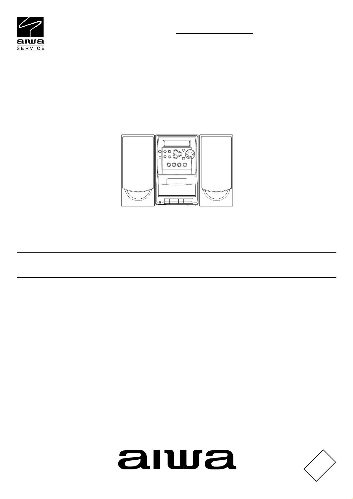
LCX-257
HR(S,L,D)
EZ (S,L,D)
K(S,L,D)
HS(L) HC(L)
SERVICE MANUAL
COMPACT DISC STEREO
SYSTEM
MODEL CODE : 86HR8-0117(B)
BASIC TAPE MECHANISM : TN-21ZSC-2003
BASIC CD MECHANISM : DA11T3C
S/M Code No. 09-006-346-6N1
DATA
Page 2

TABLE OF CONTENTS
SPECIFICATIONS .................................................................................................................................. 3
PROTECTION OF EYES FROM LASER BEAM DURING SERVICING/
Precaution to replace Optical block (SF-P101NR).................................................................................. 4
ELECTRICAL MAIN PARTS LIST ....................................................................................................... 5-8
WIRING-1 (MAIN: HC, HR)............................................................................................................... 9, 10
WIRING-2 (MAIN: HS, K, EZ ) ........................................................................................................ 11, 12
SCHEMATIC DIAGRAM-1 (MAIN 1/2)............................................................................................ 13, 14
WIRING-3 (PT)................................................................................................................................ 15, 16
SCHEMATIC DIAGRAM-2 (TUNER: HC, HR)................................................................................ 17, 18
SCHEMATIC DIAGRAM-3 (TUNER: HS, K, EZ,) ........................................................................... 19, 20
WIRING-4 (MICON/KEY/LED) ........................................................................................................ 21, 22
SCHEMATIC DIAGRAM-4 (MICON)............................................................................................... 23, 24
WIRING-5 (CD/MOTOR)................................................................................................................. 25, 26
SCHEMATIC DIAGRAM-5 (CD) ..................................................................................................... 27, 28
ELECTRICAL ADJUSTMENT-1 (HC, HR)...................................................................................... 29, 30
ELECTRICAL ADJUSTMENT-2 (HS, K, EZ) .................................................................................. 31, 32
VOLTAGE CHART........................................................................................................................... 33-35
FL (AIW4214-30PIN ACJ-11) GRID ASSIGNMENT/ANODE CONNECTION...................................... 36
TRANSISTOR ILLUSTRATION ............................................................................................................ 36
IC BLOCK DIAGRAM............................................................................................................................ 37
IC DESCRIPTION ............................................................................................................................ 38-43
MECHANICAL PARTS LIST 1/1 ........................................................................................................... 44
MECHANICAL EXPLODED VIEW 1/1............................................................................................ 45, 46
TAPE MECHANISM EXPLODED VIEW 1/1 ......................................................................................... 47
TAPE MECHANISM PARTS LIST 1/1 .................................................................................................. 48
CD MECHANISM EXPLODED VIEW 1/1 ............................................................................................. 49
CD MECHANISM PARTS LIST 1/1 ...................................................................................................... 49
SPEAKER PARTS LIST 1/1.................................................................................................................. 50
ACCESSORIES/PACKAGE LIST ......................................................................................................... 51
2
Page 3
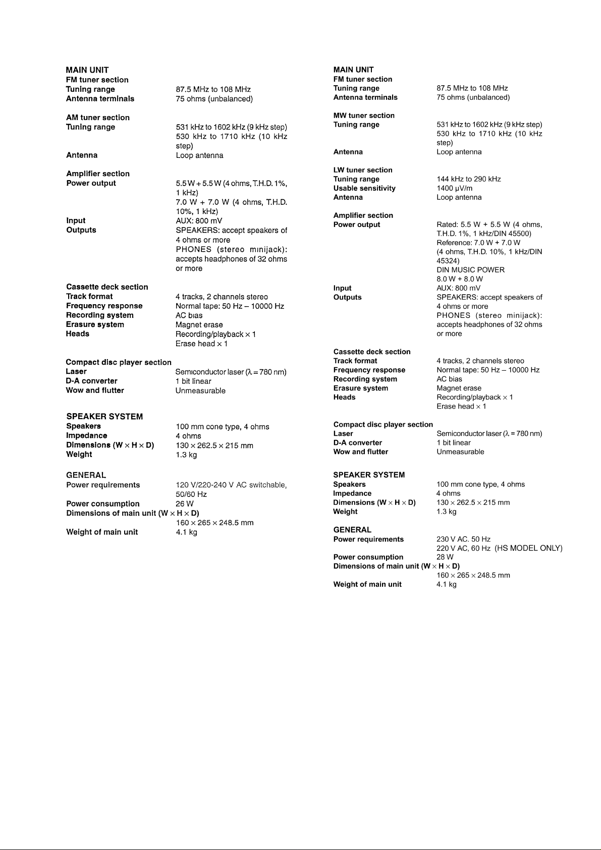
SPECIFICATIONS
HC, HR, MODELS HS, K, EZ MODELS
Design and specifications are subject to change without
•
notice
.
Design and specifications are subject to change without
•
3
notice
.
Page 4
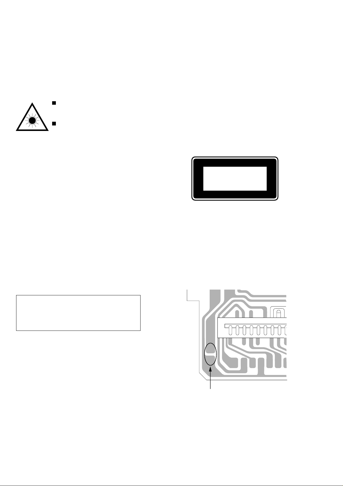
PROTECTION OF EYES FROM LASER BEAM DURING SERVICING
CLASS 1
KLASSE 1
LUOKAN 1
KLASS 1
LASER PRODUCT
LASER PRODUKT
LASER LAITE
LASER APPARAT
This set employs laser. Therefore, be sure to follow carefully the
instructions below when servicing.
WARNING!
WHEN SERVICING, DO NOT APPROACH THE LASER EXIT
WITH THE EYE TOO CLOSELY. IN CASE IT IS NECESSARY TO
CONFIRM LASER BEAM EMISSION. BE SURE TO OBSERVE
FROM A DISTANCE OF MORE THAN 30cm FROM THE
SURFACE OF THE OBJECTIVE LENS ON THE OPTICAL
PICK-UP BLOCK.
Caution: Invisible laser radiation when
open and interlocks defeated avoid exposure to beam.
Advarsel:Usynling laserståling ved åbning,
når sikkerhedsafbrydere er ude af funktion.
Undgå udsættelse for stråling.
VAROITUS!
Laiteen Käyttäminen muulla kuin tässä käyttöohjeessa mainitulla tavalla saattaa altistaa käyt-täjän turvallisuusluokan 1 ylittävälle näkymättömälle lasersäteilylle.
CAUTION
Use of controls or adjustments or performance of procedures
other than those specified herein may result in hazardous
radiation exposure.
ATTENTION
L'utilisation de commandes, réglages ou procédures autres que
ceux spécifiés peut entraîner une dangereuse exposition aux
radiations.
ADVARSEL!
Usynlig laserståling ved åbning, når sikkerhedsafbrydereer ude
af funktion. Undgå udsættelse for stråling.
This Compact Disc player is classified as a CLASS 1 LASER
product.
The CLASS 1 LASER PRODUCT label is located on the rear
exterior.
VARNING!
Om apparaten används på annat sätt än vad som specificeras i
denna bruksanvising, kan användaren utsättas för osynling
laserstrålning, som överskrider gränsen för laserklass 1.
Precaution to replace Optical block
(SF-P101NR)
Body or clothes electrostatic potential could ruin
laser diode in the optical block. Be sure ground
body and workbench, and use care the clothes
do not touch the diode.
1) After the connection, remove solder shown in
the right figure.
PICK-UP Assy P.C.B
Solder
4
Page 5

ELECTRICAL MAIN PARTS LIST
REF. NO PART NO. KANRI DESCRIPTION
NO.
IC
87-A21-368-010 IC,NJM7812FA(A)
87-A21-365-010 IC,NJM7808FA
87-002-849-080 IC,NJM78L06A
87-A21-443-040 C-IC,M62495AFP
87-A21-020-010 IC,TA8223K
87-A21-431-010 IC,BA4560N
87-A20-446-010 C-IC,LA9241ML
87-A20-459-010 C-IC,LC78622ED
87-A21-093-010 IC,LA6541D
8A-CLC-608-010 C-IC,LC877248A-5R02
87-070-127-110 IC,LC72131 D
87-A20-913-010 IC,LA1837NL
87-A21-482-010 IC,RPM6938-H4
TRANSISTOR
89-213-703-010 TR,2SB1370F
87-026-610-080 TR,KTC3198GR
89-406-555-080 TR,2SD655 (0.5W)
89-109-521-080 TR,2SA952 (0.6W)
89-109-332-380 TR,2SA933RS
89-113-187-080 TR,2SA1318TU
87-026-239-080 TR,DTC114TK (0.2W)
87-026-213-080 CHIP-TR,DTC114YK
89-112-965-080 TR,2SA1296 (0.75W)
87-026-291-080 TR,DTC124XS
87-026-263-080 C-TR,RN1410
87-026-237-080 CHIP-TR,DTC124XK
89-320-011-080 TR,2SC2001 (15W)
87-A30-072-080 C-TR,RT1P 144C
87-026-215-080 TR,DTC114YS
89-327-143-080 TR,2SC2714 (0.1W)
89-505-434-540 C-FET,2SK543(4/5)
<EXCEPT HRJS,HRD,HRL,HCL>
87-A30-086-070 C-TR,CSD1306E
<EXCEPT HRJS,HRD,HRL,HCL>
87-A30-074-080 C-TR,RT1P 141C
<EXCEPT HRJS,HRD,HRL,HCL>
DIODE
87-070-178-090 DIODE,1N5402-BD54
87-020-465-080 DIODE,1SS133 (110MA)
87-017-092-080 ZENER,HZS5C2
87-A40-189-080 DIODE,1SR139-400
87-070-345-080 DIODE,IN4148
87-017-149-080 ZENER,HZS6A2L
87-A40-270-080 C-DIODE,MC2838
<EXCEPT HRJS,HRD,HRL,HCL>
MAIN C.B
C109 87-016-440-090 CAP,E 4700-35V SME
C111 87-010-196-080 CHIP CAPACITOR,0.1-25
C112 87-010-401-080 CAP, ELECT 1-50V
C113 87-010-401-080 CAP, ELECT 1-50V
C114 87-010-101-080 CAP, ELECT 220-16
C115 87-010-101-080 CAP, ELECT 220-16
C117 87-010-403-080 CAP, ELECT 3.3-50V
C118 87-010-101-080 CAP, ELECT 220-16
C119 87-010-196-080 CHIP CAPACITOR,0.1-25
C120 87-010-263-080 CAP, ELECT 100-10V
C201 87-010-248-080 CAP, ELECT 220-10V
C203 87-010-248-080 CAP, ELECT 220-10V
C204 87-010-197-080 CAP, CHIP 0.01 DM
C207 87-010-196-080 C-CAP,S 0.1-25 F
<EXCEPT HRJS,HRD,HRL,HCL>
C208 87-010-196-080 C-CAP,S 0.1-25 F
<EXCEPT HRJS,HRD,HRL,HCL>
REF. NO PART NO. KANRI DESCRIPTION
NO.
C213 87-010-196-080 CHIP CAPACITOR,0.1-25
C214 87-010-196-080 CHIP CAPACITOR,0.1-25
C223 87-A11-126-080 CAP,TC U 3300P-50 K B
<HRJS,HRD,HRL,HCL>
C224 87-A11-126-080 CAP,TC U 3300P-50 K B
<HRJS,HRD,HRL,HCL>
C225 87-010-401-080 CAP, ELECT 1-50V
C226 87-010-401-080 CAP, ELECT 1-50V
C227 87-018-208-080 CAP 0.047-50F
C228 87-018-208-080 CAP 0.047-50F
C229 87-018-132-080 CAP, CER 2200P-16V
C230 87-018-132-080 CAP, CER 2200P-16V
C231 87-010-406-080 CAP, ELECT 22-50
C232 87-010-406-080 CAP, ELECT 22-50
C233 87-010-260-080 CAP, ELECT 47-25V
C234 87-010-404-080 CAP, ELECT 4.7-50V
C235 87-010-112-080 CAP, ELECT 100-16V
C236 87-010-112-080 CAP, ELECT 100-16V
C237 87-010-237-080 CAP, ELECT 1000-16V
C238 87-010-237-080 CAP, ELECT 1000-16V
C241 87-018-209-080 CAP, CER 0.1-50V
C243 87-010-387-080 CAP,E 470-25 SME
C244 87-010-248-080 CAP, ELECT 220-10V
C247 87-010-318-080 C-CAP,S 47P-50 CH
<EXCEPT HRJS,HRD,HRL,HCL>
C248 87-010-318-080 C-CAP,S 47P-50 CH
<EXCEPT HRJS,HRD,HRL,HCL>
C250 87-010-401-080 CAP, ELECT 1-50V
C251 87-010-401-080 CAP, ELECT 1-50V
C255 87-010-401-080 CAP, ELECT 1-50V
C256 87-010-401-080 CAP, ELECT 1-50V
C257 87-010-401-080 CAP, ELECT 1-50V
C258 87-010-401-080 CAP, ELECT 1-50V
C259 87-010-401-080 CAP, ELECT 1-50V
C260 87-010-401-080 CAP, ELECT 1-50V
C270 87-010-322-080 C-CAP,S 100P-50 CH
C271 87-010-322-080 C-CAP,S 100P-50 CH
C301 87-010-322-080 C-CAP,S 100P-50 CH
C302 87-010-401-080 CAP, ELECT 1-50V
C305 87-010-374-080 CAP, ELECT 47-10V
C307 87-010-405-080 CAP, ELECT 10-50V
C308 87-010-248-080 CAP, ELECT 220-10V
C309 87-010-405-080 CAP, ELECT 10-50V
C310 87-010-322-080 C-CAP,S 100P-50 CH
C312 87-010-374-080 CAP, ELECT 47-10V
C313 87-010-401-080 CAP, ELECT 1-50V
C315 87-010-426-080 C-CAP,S 0.012-25 B
C318 87-010-426-080 C-CAP,S 0.012-25 B
C319 87-A11-098-080 CAP,270PF-50 CH
C320 87-010-197-080 CAP, CHIP 0.01 DM
C322 87-010-248-080 CAP, ELECT 220-10V
C324 87-010-186-080 CAP,CHIP 4700P
C327 87-010-405-080 CAP, ELECT 10-50V
C328 87-010-405-080 CAP, ELECT 10-50V
C329 87-010-178-080 CHIP CAP 1000P
C330 87-010-178-080 CHIP CAP 1000P
C331 87-010-178-080 CHIP CAP 1000P
C332 87-010-263-080 CAP, ELECT 100-10V
C334 87-010-401-080 CAP, ELECT 1-50V
C335 87-010-260-080 CAP, ELECT 47-25V
C341 87-010-197-080 CAP, CHIP 0.01 DM
C701 87-010-381-080 CAP, ELECT 330-16V
C702 87-010-404-080 CAP, ELECT 4.7-50V
C703 87-012-286-080 CAP, U 0.01-25
C704 87-012-286-080 CAP, U 0.01-25
C705 87-A10-592-080 C-CAP,S 0.015-50 J B
<HRJS,HRD,HRL,HCL>
C706 87-A10-592-080 C-CAP,S 0.015-50 J B
<HRJS,HRD,HRL,HCL>
C709 87-012-195-080 C-CAP,U 100P-50CH
C711 87-010-260-080 CAP, ELECT 47-25V
5
Page 6

REF. NO PART NO. KANRI DESCRIPTION
NO.
C712 87-010-831-080 C-CAP,U,0.1-16F
C714 87-012-286-080 CAP, U 0.01-25
C715 87-012-195-080 C-CAP,U 100P-50CH
<EXCEPT HRJS,HRD,HRL,HCL>
C717 87-012-286-080 CAP, U 0.01-25
C719 87-012-286-080 CAP, U 0.01-25
C720 87-012-195-080 C-CAP,U 100P-50CH
C721 87-012-176-080 CAP 15P
C722 87-012-176-080 CAP 15P
C723 87-018-131-080 CAP, CER 1000P-50V
C725 87-018-131-080 CAP, CER 1000P-50V
C727 87-010-196-080 CHIP CAPACITOR,0.1-25
C728 87-010-248-080 CAP, ELECT 220-10V
C729 87-012-274-080 CHIP CAP,U 1000P-50B
C731 87-012-286-080 CAP, U 0.01-25
C733 87-010-987-080 C-CAP,S 1500P-50 CH
<HRJS,HRD,HRL,HCL>
C733 87-012-280-080 CAP, U 3300P-50
<EXCEPT HRJS,HRD,HRL,HCL>
C734 87-010-987-080 C-CAP,S 1500P-50 CH
<HRJS,HRD,HRL,HCL>
C734 87-012-280-080 CAP, U 3300P-50
<EXCEPT HRJS,HRD,HRL,HCL>
C735 87-A10-592-080 C-CAP,S 0.015-50 J B
<HRJS,HRD,HRL,HCL>
C736 87-A10-592-080 C-CAP,S 0.015-50 J B
<HRJS,HRD,HRL,HCL>
C737 87-010-987-080 C-CAP,S 1500P-50 CH
<HRJS,HRD,HRL,HCL>
C738 87-010-987-080 C-CAP,S 1500P-50 CH
<HRJS,HRD,HRL,HCL>
C751 87-010-220-080 C-CAP,S 0.018-25 B
<HRJS,HRD,HRL,HCL>
C752 87-010-220-080 C-CAP,S 0.018-25 B
<HRJS,HRD,HRL,HCL>
C752 87-012-282-080 CAP, U 4700P-50
<EXCEPT HRJS,HRD,HRL,HCL>
C753 87-012-195-080 C-CAP,U 100P-50CH
<EXCEPT HRJS,HRD,HRL,HCL>
C755 87-012-286-080 CAP, U 0.01-25
<EXCEPT HRJS,HRD,HRL,HCL>
C756 87-012-286-080 CAP, U 0.01-25
C757 87-012-188-080 C-CAP,U 47P-50 CH
C758 87-012-167-080 C-CAP,U 5P-50 CH
C761 87-010-196-080 CHIP CAPACITOR,0.1-25
<EXCEPT HRJS,HRD,HRL,HCL>
C762 87-012-286-080 CAP, U 0.01-25
<EXCEPT HRJS,HRD,HRL,HCL>
C763 87-010-829-080 CAP, U 0.047-16
C764 87-012-337-080 C-CAP,U 56P-50 CH
<HRJS,HRD,HRL,HCL>
C765 87-012-286-080 CAP, U 0.01-25
C766 87-010-197-080 CAP, CHIP 0.01 DM
<EXCEPT HRJS,HRD,HRL,HCL>
C766 87-010-197-080 CAP, CHIP 0.01 DM
<EXCEPT HRJS,HRD,HRL,HCL>
C768 87-012-286-080 CAP, U 0.01-25
C769 87-010-260-080 CAP, ELECT 47-25V
C770 87-010-829-080 CAP, U 0.047-16
C771 87-010-383-080 CAP, ELECT 33-25V
C772 87-010-829-080 CAP, U 0.047-16
C773 87-010-196-080 CHIP CAPACITOR,0.1-25
C774 87-010-263-080 CAP, ELECT 100-10V
C775 87-010-404-080 CAP, ELECT 4.7-50V
C776 87-012-286-080 CAP, U 0.01-25
C777 87-010-400-080 CAP, ELECT 0.47-50V
<HRJS,HRD,HRL,HCL>
C777 87-010-493-080 CAP,E 0.47-50 GAS
<EXCEPT HRJS,HRD,HRL,HCL>
C778 87-010-401-080 CAP, ELECT 1-50V
C779 87-010-401-080 CAP, ELECT 1-50V
C779 87-010-829-080 CAP, U 0.047-16
C780 87-010-196-080 CHIP CAPACITOR,0.1-25
REF. NO PART NO. KANRI DESCRIPTION
NO.
C781 87-010-405-080 CAP, ELECT 10-50V
C782 87-010-405-080 CAP, ELECT 10-50V
C783 87-012-286-080 CAP, U 0.01-25
C784 87-012-286-080 CAP, U 0.01-25
C785 87-010-402-080 CAP, ELECT 2.2-50V
<EXCEPT HRJS,HRD,HRL,HCL>
C785 87-016-279-080 CAP,E 1-50 BP<HRJS,HRD,HRL,HCL>
C786 87-010-402-080 CAP, ELECT 2.2-50V
<EXCEPT HRJS,HRD,HRL,HCL>
C786 87-016-279-080 CAP,E 1-50 BP<HRJS,HRD,HRL,HCL>
C787 87-012-275-080 C-CAP,U 1200P-50 B
<EXCEPT HRJS,HRD,HRL,HCL>
C788 87-012-275-080 C-CAP,U 1200P-50 B
<EXCEPT HRJS,HRD,HRL,HCL>
C789 87-012-275-080 C-CAP,U 1200P-50 B
C790 87-012-275-080 C-CAP,U 1200P-50 B
C791 87-010-405-080 CAP, ELECT 10-50V
C793 87-012-273-080 C-CAP,U 820P-50 B
C794 87-010-406-080 CAP, ELECT 22-50
C795 87-010-596-080 CAP, S 0.047-16
C796 87-010-403-080 CAP, ELECT 3.3-50V
C797 87-012-276-080 CAP, CHIP SS 1500 PBK
<EXCEPT HRJS,HRD,HRL,HCL>
C798 87-012-276-080 CAP, CHIP SS 1500 PBK
<EXCEPT HRJS,HRD,HRL,HCL>
C812 87-012-286-080 CAP, U 0.01-25
C814 87-012-286-080 CAP, U 0.01-25
<EXCEPT HRJS,HRD,HRL,HCL>
C820 87-010-260-080 CAP, ELECT 47-25V
C821 87-012-286-080 CAP, U 0.01-25
C822 87-012-286-080 CAP, U 0.01-25
C823 87-012-286-080 CAP, U 0.01-25
C828 87-010-196-080 CHIP CAPACITOR,0.1-25
C829 87-010-196-080 CHIP CAPACITOR,0.1-25
C830 87-010-406-080 CAP, ELECT 22-50
<EXCEPT HRJS,HRD,HRL,HCL>
C940 87-012-286-080 CAP, U 0.01-25
<EXCEPT HRJS,HRD,HRL,HCL>
C942 87-012-168-080 C-CAP,U 6P-50 CH
<EXCEPT HRJS,HRD,HRL,HCL>
C947 87-012-286-080 CAP, U 0.01-25
<EXCEPT HRJS,HRD,HRL,HCL>
C949 87-A10-039-080 C-CAP,U 470P-50 J CH
<EXCEPT HRJS,HRD,HRL,HCL>
C952 87-012-286-080 CAP, U 0.01-25
<EXCEPT HRJS,HRD,HRL,HCL>
C958 87-010-197-080 CAP, CHIP 0.01 DM
<EXCEPT HRJS,HRD,HRL,HCL>
C959 87-010-831-080 C-CAP,U,0.1-16F<HRJS,HRD,HRL,HCL>
C960 87-010-196-080 CHIP CAPACITOR,0.1-25
C961 87-012-174-080 C-CAP,U 12P-50 J CH
<HRJS,HRD,HRL,HCL>
C962 87-010-401-080 CAP, ELECT 1-50V
<EXCEPT HRJS,HRD,HRL,HCL>
C963 87-010-196-080 CHIP CAPACITOR,0.1-25
<HRJS,HRD,HRL,HCL>
CF801 87-008-423-010 CERAMIC FILTER, SFE10.7
<EXCEPT HRJS,HRD,HRL,HCL>
CF801 87-008-261-010 FILTER, SFE10.7MA5-A
<HRJS,HRD,HRL,HCL>
CF802 82-785-747-010 CF MS2 GHY R
<EXCEPT HRJS,HRD,HRL,HCL>
CF802 87-008-261-010 FILTER, SFE10.7MA5-A
<HRJS,HRD,HRL,HCL>
CN101 87-049-919-010 CONN,3P EH V WHT
CN201 87-099-719-010 CONN,30P TYK-B(X)
CN203 87-A60-060-010 CONN,07P V 9604S-07C
CN301 87-A60-627-010 CONN,10P V 2MM JMT
FB202 87-008-372-080 FILTER,EMI BL OIRNI
<EXCEPT HRJS,HRD,HRL,HCL>
FB203 87-008-372-080 FILTER,EMI BL OIRNI
<EXCEPT HRJS,HRD,HRL,HCL>
FB701 87-008-372-080 FILTER, EMI BL OIRNI
6
Page 7

REF. NO PART NO. KANRI DESCRIPTION
FFE801 A8-6ZA-19C-170 6ZA-1 YFEENC
FFE801 A8-8ZA-193-070 8ZA-1 YFEUNC<HRJS,HRD,HRL,HCL>
!
ICP203 87-001-132-080 ICP-N38
J201 87-A60-420-010 JACK,3.5 ST (MSC)
J202 87-A60-754-010 TERMINAL,SPK 4P MSP-154V-05
J203 87-A60-881-010 JACK,PIN 2P MSP 242V05 PBSN
J204 87-099-801-010 JACK,PIN 1P BLK
J801 87-A60-202-010 TERMINAL,ANT 4P MSP-154V-02
J801 87-033-241-010 TERMINAL,ANT AJ-2039
L204 87-005-239-080 COIL,100UH
L205 87-005-239-080 COIL,100UH
L301 87-007-342-010 COIL,OSC 85K BIAS
L771 87-A50-266-010 COIL,FM DET-2N(TOK)
L772 87-A91-110-010 FLTR,PCFJZH-450 (TOK)
L781 87-005-847-080 COIL,2.2UH(CECS)
L832 87-005-847-080 COIL,2.2UH(CECS)
L941 87-A50-020-010 COIL,ANT LW(COI)
L942 87-A50-019-010 COIL,OSC LW(COI)
L981 8Z-ZA1-665-010 COIL,AM PACK 2(TOK)
L981 8Z-ZA1-667-010 COIL,AM PACK 4F(TOK)
R251 87-029-124-010 RES,FUSE 2.2-1/4
R252 87-029-124-010 RES,FUSE 2.2-1/4
S301 8Z-CL8-668-010 SW,RP ZCL8
TC942 87-011-253-080 TRIMER,30P LAR
X721 87-A70-061-010 VIB,XTAL 4.500MHZ CSA-309
MICON C.B
C601 87-010-196-080 CHIP CAPACITOR,0.1-25
C602 87-010-248-080 CAP, ELECT 220-10V
C606 87-010-178-080 CHIP CAP 1000P
C607 87-010-317-080 C-CAP,S 39P-50 CH
C608 87-010-312-080 C-CAP,S 15P-50 CH
C609 87-010-315-080 C-CAP,S 27P-50 CH
C610 87-010-452-080 CAPACITOR,1-16
C613 87-010-196-080 CHIP CAPACITOR,0.1-25
C614 87-010-196-080 CHIP CAPACITOR,0.1-25
C618 87-012-156-080 C-CAP,S 220P-50 CH
C619 87-010-196-080 CHIP CAPACITOR,0.1-25
C621 87-010-196-080 CHIP CAPACITOR,0.1-25
C622 87-010-401-080 CAP, ELECT 1-50V
C641 87-010-248-080 CAP, ELECT 220-10V
CN601 87-099-720-010 CONN,30P TYK-B(P)
CN602 87-A60-059-010 CONN,08P V 9604S-08C
CN604 87-A60-060-010 CONN,07P V 9604S-07C
L601 87-003-098-080 COIL,2.2UH
L603 87-003-098-080 COIL,2.2UH
LCD601 8A-CJB-630-010 LCD,AIW4214-30P1N ACJ-11
X601 87-030-376-080 VIB,CER CSA5.76MG200
CD C.B
C401 87-010-403-080 CAP, ELECT 3.3-50V
C402 87-010-197-080 CAP, CHIP 0.01 DM
C403 87-010-263-080 CAP, ELECT 100-10V
C404 87-010-248-080 CAP, ELECT 220-10V
C405 87-010-197-080 CAP, CHIP 0.01 DM
C406 87-010-374-080 CAP, ELECT 47-10V
C407 87-010-178-080 CHIP CAP 1000P
C408 87-010-198-080 CAP, CHIP 0.022
C409 87-010-248-080 CAP, ELECT 220-10V
C410 87-010-263-080 CAP, ELECT 100-10V
NO.
<EXCEPT HRJS,HRD,HRL,HCL>
<HRJS,HRD,HRL,HCL>
<EXCEPT HRJS,HRD,HRL,HCL>
<EXCEPT HRJS,HRD,HRL,HCL>
<EXCEPT HRJS,HRD,HRL,HCL>
<EXCEPT HRJS,HRD,HRL,HCL>
<EXCEPT HRJS,HRD,HRL,HCL>
<EXCEPT HRJS,HRD,HRL,HCL>
<HRJS,HRD,HRL,HCL>
<EXCEPT HRJS,HRD,HRL,HCL>
C411 87-A11-177-080 C-CAP,S 0.15-16 K B
C412 87-010-401-080 CAP, ELECT 1-50V
C413 87-016-369-080 C-CAP,S 0.033-25 B K
C414 87-010-405-080 CAP, ELECT 10-50V
C416 87-010-545-080 CAP, ELECT 0.22-50V
C417 87-012-157-080 C-CAP,S 330P-50 CH
C418 87-010-213-080 C-CAP,S 0.015-50 B
C419 87-A10-201-080 C-CAP,S0.33-16 KB
C420 87-016-369-080 C-CAP,S 0.033-25 B K
C421 87-A11-177-080 C-CAP,S 0.15-16 K B
C422 87-010-184-080 CHIP CAPACITOR 3300P(K)
C423 87-010-992-080 C-CAP,S 0.047-25 B
C424 87-016-460-080 C-CAP,S 0.22-16 B
C425 87-010-176-080 C-CAP,S 680P-50 SL
C426 87-A10-201-080 C-CAP,S0.33-16 KB
C428 87-010-197-080 CAP, CHIP 0.01 DM
C429 87-010-186-080 CAP,CHIP 4700P
C430 87-012-156-080 C-CAP,S 220P-50 CH
C431 87-010-545-080 CAP, ELECT 0.22-50V
C432 87-010-374-080 CAP, ELECT 47-10V
C433 87-010-401-080 CAP, ELECT 1-50V
C434 87-010-184-080 CHIP CAPACITOR 3300P(K)
C435 87-010-197-080 CAP, CHIP 0.01 DM
C436 87-010-374-080 CAP, ELECT 47-10V
C437 87-010-404-080 CAP, ELECT 4.7-50V
C438 87-016-669-080 C-CAP,S 0.1-25 K B
C439 87-010-178-080 CHIP CAP 1000P
C440 87-010-145-080 C-CAP,S 1P-50 CH
C441 87-010-197-080 CAP, CHIP 0.01 DM
C442 87-010-313-080 CAP, CHIP 18P
C445 87-010-196-080 CHIP CAPACITOR,0.1-25
C446 87-010-196-080 CHIP CAPACITOR,0.1-25
C447 87-010-196-080 CHIP CAPACITOR,0.1-25
C448 87-010-315-080 C-CAP,S 27P-50 CH
C450 87-012-140-080 CAP 470P
C451 87-012-156-080 C-CAP,S 220P-50 CH
C455 87-010-247-080 CAP, ELECT 100-50V
C457 87-010-316-080 C-CAP,S 33P-50 CH
C458 87-010-316-080 C-CAP,S 33P-50 CH
C459 87-010-263-080 CAP, ELECT 100-10V
C460 87-015-819-080 CAPACITOR,0.01
C461 87-010-197-080 CAP, CHIP 0.01 DM
C462 87-010-221-080 CAP, ELECT 470-10V
C463 87-A11-144-080 CAP,TC U 0.1-50 K B
C465 87-010-404-080 CAP, ELECT 4.7-50V
C466 87-010-196-080 CHIP CAPACITOR,0.1-25
C467 87-010-263-080 CAP, ELECT 100-10V
C469 87-012-154-080 C-CAP,S 150P-50 CH
C470 87-010-544-080 CAP, ELECT 0.1-50V
C471 87-015-785-080 CHIP CAPACITOR, 0.1FZ-25Z
C472 87-015-785-080 CHIP CAPACITOR, 0.1FZ-25Z
C473 87-015-785-080 CHIP CAPACITOR, 0.1FZ-25Z
C474 87-015-785-080 CHIP CAPACITOR, 0.1FZ-25Z
C475 87-010-197-080 CAP, CHIP 0.01 DM
C476 87-010-236-080 CAP,E 1000-10 SME
C477 87-010-197-080 CAP, CHIP 0.01 DM
C478 87-010-265-080 CAP, ELECT 33-16V
C479 87-010-197-080 CAP, CHIP 0.01 DM
C480 87-010-221-080 CAP, ELECT 470-10V
C481 87-010-405-080 CAP, ELECT 10-50V
C482 87-010-405-080 CAP, ELECT 10-50V
C489 87-010-196-080 CHIP CAPACITOR,0.1-25
C490 87-010-196-080 CHIP CAPACITOR,0.1-25
C491 87-010-197-080 CAP, CHIP 0.01 DM
C492 87-010-221-080 CAP, ELECT 470-10V
C494 87-A11-144-080 CAP,TC U 0.1-50 K B
C501 87-010-196-080 CHIP CAPACITOR,0.1-25
C502 87-010-322-080 C-CAP,S 100P-50 CH
C503 87-010-322-080 C-CAP,S 100P-50 CH
C504 87-010-322-080 C-CAP,S 100P-50 CH
REF. NO PART NO. KANRI DESCRIPTION
NO.
REF. NO PART NO. KANRI DESCRIPTION
NO.
C505 87-010-322-080 C-CAP,S 100P-50 CH
C506 87-010-322-080 C-CAP,S 100P-50 CH
C510 87-016-669-080 C-CAP,S 0.1-25 K B
CN401 87-A60-424-010 CONN,16P V TOC-B
CN403 87-A60-079-010 CONN,08P H 9604S-08F
CN405 87-A60-060-010 CONN,07P V 9604S-07C
CN406 87-A60-619-010 CONN,2P V 2MM JMT
CNA402 8A-CJB-623-010 CONN ASSY,6P CD MOTOR
L401 87-003-102-080 COIL, 10UH
L402 87-005-847-080 COIL,2.2UH(CECS)
L404 87-003-152-080 COIL, 100UH
L450 87-005-847-080 COIL,2.2UH(CECS)
SFR430 87-024-437-080 SFR100K,RH063EC
X401 87-A70-046-010 VIB,XTAL 16.934MHZ
KEY C.B
C901 87-010-196-080 CHIP CAPACITOR,0.1-25
C902 87-010-196-080 CHIP CAPACITOR,0.1-25
C903 87-010-197-080 CAP, CHIP 0.01 DM
C904 87-010-197-080 CAP, CHIP 0.01 DM
C905 87-010-405-080 CAP, ELECT 10-50V
C906 87-010-178-080 CHIP CAP 1000P
CN901 87-A60-080-010 CONN,07P H 9604S-07F
S901 87-A91-024-180 SW,TACT KSH0611BT
S902 87-A91-024-180 SW,TACT KSH0611BT
S904 87-A91-024-180 SW,TACT KSH0611BT
S905 87-A91-024-180 SW,TACT KSH0611BT
S906 87-A91-024-180 SW,TACT KSH0611BT
S907 87-A91-024-180 SW,TACT KSH0611BT
S908 87-A91-024-180 SW,TACT KSH0611BT
S909 87-A91-024-180 SW,TACT KSH0611BT
S910 87-A91-024-180 SW,TACT KSH0611BT
S911 87-A91-024-180 SW,TACT KSH0611BT
S913 87-A91-024-180 SW,TACT KSH0611BT
S915 87-A91-024-180 SW,TACT KSH0611BT
S916 87-A91-024-180 SW,TACT KSH0611BT
REF. NO PART NO. KANRI DESCRIPTION
S917 87-A91-024-180 SW,TACT KSH0611BT
S920 87-A91-385-010 SW,RTRY EC12E12504-15MM
LED C.B
CN606 87-A61-297-010 CONN,5P TKX-P05P-A1
D621 87-A40-821-080 LED,SMLS1BE16C BLU/UMB
D622 87-A40-821-080 LED,SMLS1BE16C BLU/UMB
PT C.B
C100 87-010-398-010 CAP ELECT 2200
C101 87-010-198-080 CAP, CHIP 0.022
C102 87-010-198-080 CAP, CHIP 0.022
C103 87-010-198-080 CAP, CHIP 0.022
C104 87-010-198-080 CAP, CHIP 0.022
CNA101 8A-CLC-610-010 CONN ASSY,3P POWER
!
F101 87-035-367-010 FUSE, 3.15A 250V
FC101 87-A90-505-080 FUSE CLAMP,TP00351-51
FC102 87-A90-505-080 FUSE CLAMP,TP00351-51
!
PT101 8A-CLC-611-010 PT,ACL-12 E
!
PT101 8A-CLC-609-010 PT,ACL-12 H<HRJS,HRD,HRL,HCL>
S101 87-A90-234-010 SW,SL 1-2-2 SW2201
!
T1 87-A60-317-010 TERMINAL, 1P MSC
!
T2 87-A60-317-010 TERMINAL, 1P MSC
MOTOR C.B
M2 9X-262-576-910 MOTOR GEAR ASSY
PIN3 91-564-722-110 CONNECTOR 6P
SW1 91-572-085-120 LEAF SW
NO.
<EXCEPT HRJS,HRD,HRL,HCL>
• Regarding connectors, they are not stocked as they are not the initial order items.
The connectors are available after they are supplied from connector manufacturers upon the order is received.
CHIP RESISTOR PART CODE
Chip Resistor Part Coding
88
A
Resistor Code
Chip resistor
Wattage Type Tolerance
1/16W 1005 5% CJ
1/16W
1/10W
1/8W
1608
2125
3216
5%
5%
5%
Symbol
Figure
Value of resistor
CJ
CJ
CJ
Form
L
W
Dimensions (mm)
LW t
1.0 0.5 0.35 104
t
1.6 0.8 0.45
2 1.25 0.45
1.6
0.55
3.2
<HRJS,HRD,HRL,HCL>
: A
Resistor Code
: A
108
118
128
87
Page 8
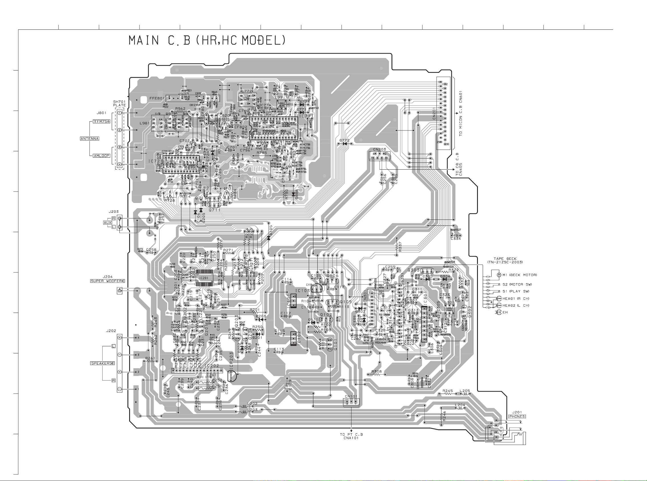
WIRING-1 (MAIN: HC, HR)
1
A
B
C
D
234567
8
9
10
11 12 13
14
E
F
G
H
I
J
K
109
Page 9

WIRING-2 (MAIN: HS, K, EZ )
1
A
B
C
D
234567
8
9
10
11 12 13
14
E
F
G
H
I
J
K
1211
Page 10
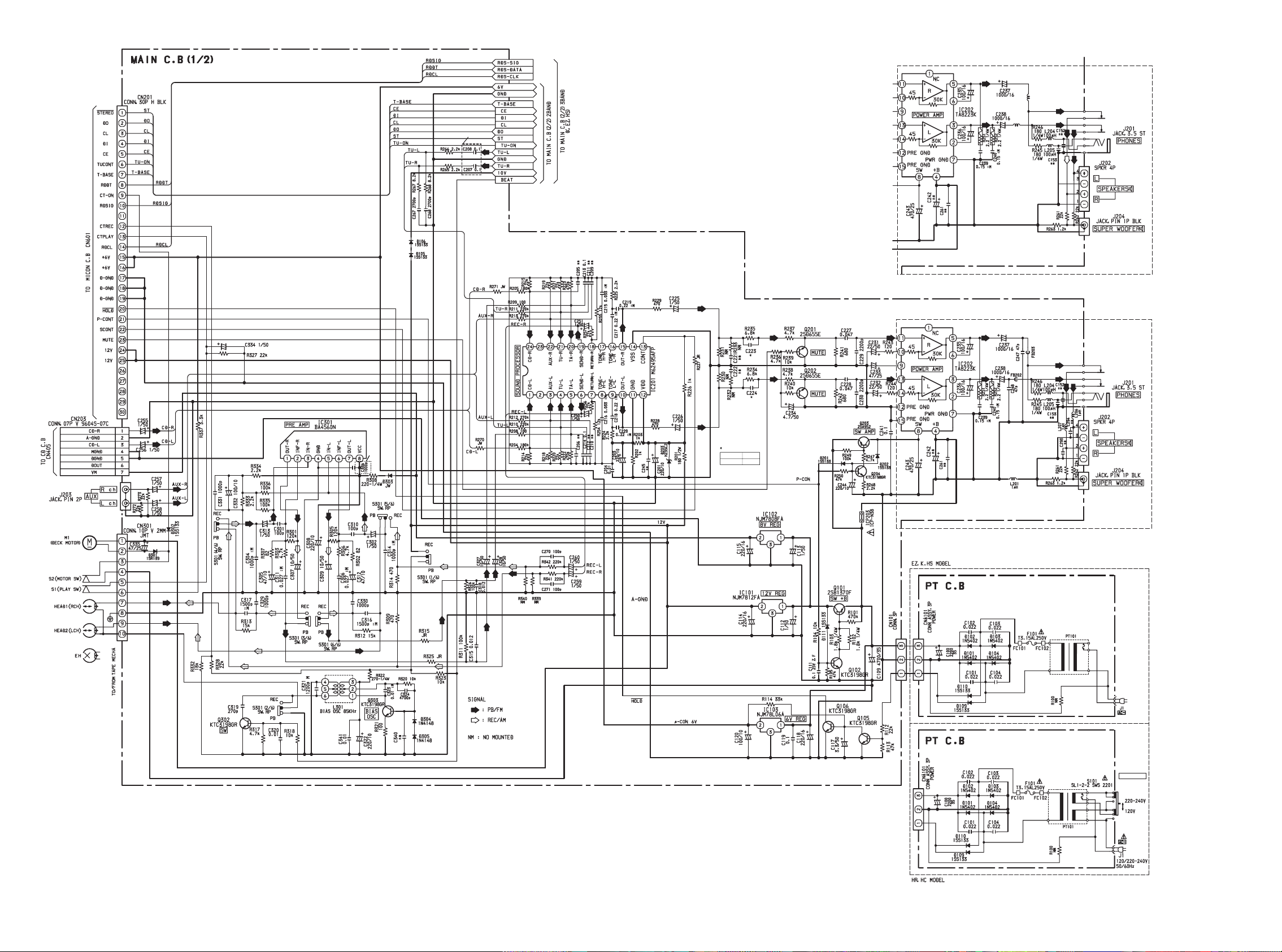
SCHEMATIC DIAGRAM-1 (MAIN 1/2)
HC, HR MODELS
K,EZ,HS
(HC, HR)
K, EZ, HS MODELS
L202
JW
J203
JW
TAPE DECK
(TN-21ZSC-2003)
K,EZ
HS
C223, 224
HC, HR
K, EZ, HS
3300p
nm
230V
50Hz
(K,EZ)
220V
60Hz
(HS)
S101
AC VOLTAGE
1413
Page 11
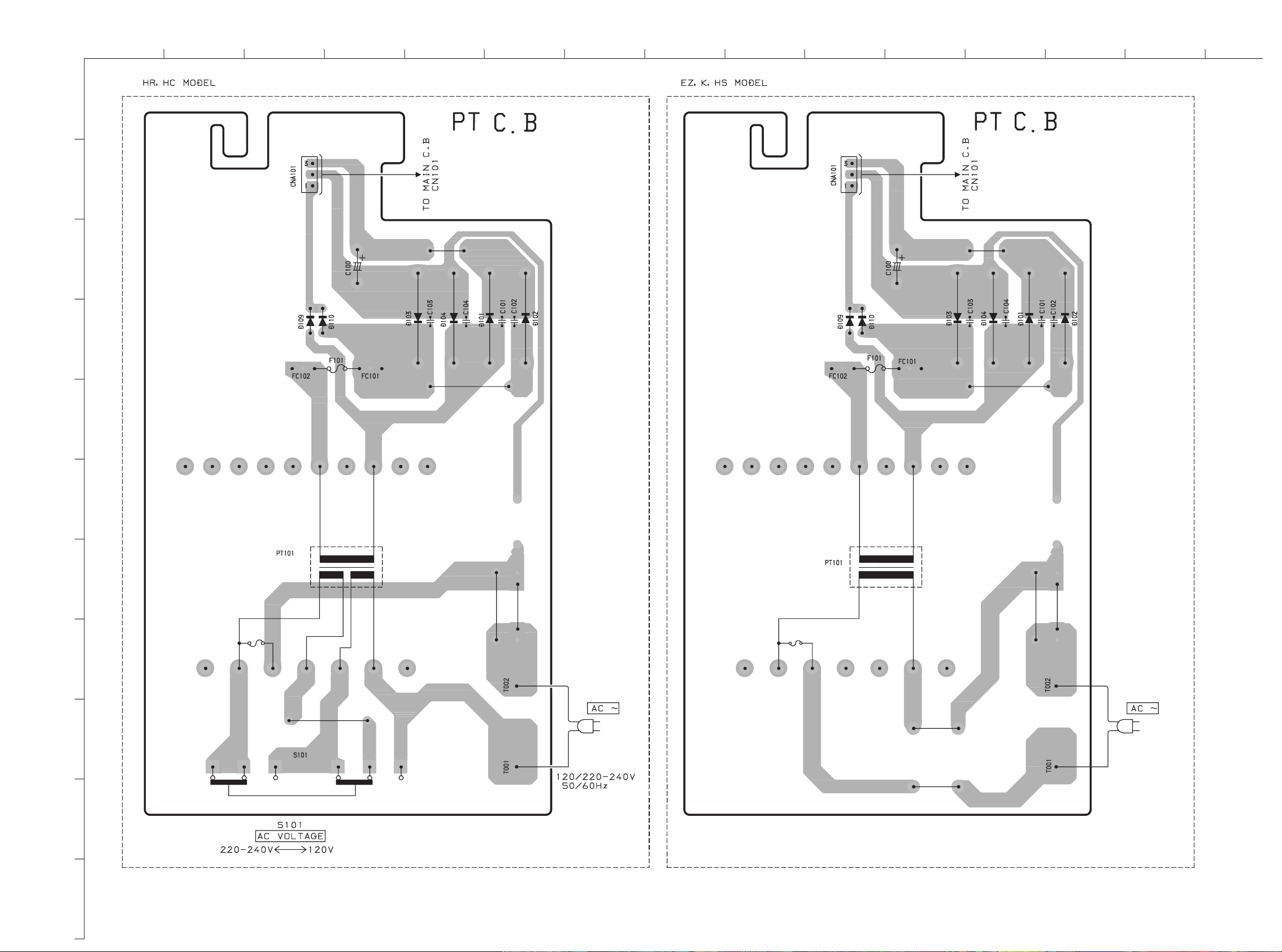
WIRING-3 (PT)
1
A
B
C
D
234567
8
9
10
11 12 13
14
E
F
G
H
I
230V 50Hz (K, EZ)
220V 60Hz (HS)
J
K
1615
Page 12

SCHEMATIC DIAGRAM-2 (TUNER: HC, HR)
1817
Page 13

SCHEMATIC DIAGRAM-3 (TUNER: HS, K, EZ,)
L981 (3/3)
MW VT ADJ.
L981 (1/3)
MW TRACKING ADJ.
L942
LW VT ADJ.
L941, TC942
LW TRACKING ADJ.
2019
Page 14

WIRING-4 (MICON/KEY/LED)
1
A
B
C
D
234567
8
9
10
11 12 13
14
30
E
50
51
F
31
1
100
81
80
G
H
I
J
K
2221
Page 15

SCHEMATIC DIAGRAM-4 (MICON)
2423
Page 16

WIRING-5 (CD/MOTOR)
1
234567
8
9
10
11 12 13
14
A
MOTOR C.B
M2
+
B
(SLED MOTOR)
_
M2
SW1
(INSIDE LIMIT SW)
C
(SPINDLE MOTOR)
M3
SW1
PIN3
_
D
+
M3
E
F
G
H
I
J
K
2625
Page 17

SCHEMATIC DIAGRAM-5 (CD)
2827
Page 18

ELECTRICAL ADJUSTMENT-1 (HC, HR)
MAIN C.B
5
L301
L771
4
IC772
1
L772
(RED)
2
IC721
(YELLOW)
L981
3
J201
PHONS
MICON C.B
IC404
SFR430
6
3029
Page 19

ELECTRICAL ADJUSTMENT-2 (HS, K, EZ)
MAIN C.B
7
L301
6
L771
3
L772
IC771
1
L942
(RED)
4
TC942
(YELLOW)
L981
5
2
L941
J201
PHONES
MICON C.B
IC404
SFR430
8
3231
Page 20

VOLTAGE CHART
3433
Page 21

35
Page 22

FL (AIW4214-30PIN ACJ-11) GRID ASSIGNMENT/ANODE CONNECTION
GRID ASSIGNMENT
ANODE CONNECTION
TRANSISTOR ILLUSTRATION
C
B
E
2SC2714
DTC114TK
RT1P141C
ECB ECB ECB
2SA1296
KTC3198
DTC114YS
PT1P144C
DTC124XK
DTC114YK
RN1410
DTC124XS
36
2SA933
2SC2001
2SD655
2SA952
2SA1318
S
D
2SK543
G
ECB
2SB1370F
Page 23

IC BLOCK DIAGRAM
IC, M62495AFP
IC, LA6541D
IC, LA1837NL
IC, BA4560N
IC, LC72131D
37
Page 24

IC DESCRIPTION
IC, LC877248A-5R02
Pin No. Pin Name I/O Description
1
O-ARDY
O
10
11
12
13
14
15
16
17
18
2
3
4
5
6
7
8
9
O-SREQ
O-SOUT
I-SIN
I-ACLK
I-MREQ
NC (SELECT)
O-PCONT
___________
I-HOLD
O-CLKSFT
I-RESET
XT1
XT2
VSS1
CF1
CF2
VDD1
I-JOGA
—
—
O
O
Not connected.
I
I
I
O
Pull down.
O
Main power control.
I
Hold status detection.
O
Clock shift control.
I
Reset terminal.
I
Connected to VDD.
O
Not connected.
GND.
I
External ceramics oscillator (5.76 MHz) is connected to this pin (input).
O
External ceramics oscillator (5.76 MHz) is connected to this pin (output).
Power supply positive polarity (+) terminal.
I
Jog dial detection A.
19
20
21
22
23
24
25
26
27
28
29
30
31
32
33
34
35
I-JOGB
I-KEY1
I-KEY
I-RDSIG
I-CTON
I-RDDT
I-COLOR
I-TMBASE
I-INIT
I-RDCL
I-RMC
I-CTPLAY
I-CTREC
O-TUCONT
O-TUCE
O-TUDI
O-TUCL
I
Jog dial detection B.
I
Tact key, AD input detection.
I
I
RDS signal level input, AD input.
I
CT DECK power supply detection.
I
RDS data input.
I
LCD back light initial setting input.
I
8Hz clock reference frequency input.
I
Tuner destination, initial setting input.
I
RDS clock input.
I
Remote controller receptor signal input.
I
CT DECK PLAY detection.
I
CT DECK REC detection.
O
Tuner power supply control.
O
Tuner, Chip enable output for PLL communication.
O
Tuner, Serial data output for PLL communication.
O
Tuner, Clock output for PLL communication.
36
37
38
39-53
54
55
I-TUDO
_________________
I-STEREO
NC
S9-S23
VDD2
VCC2
—
—
—
I
Tuner, Serial data input for PLL communication.
I
Tuner stereo reception detection.
Not connected.
O
LCD SEG terminal initial setting output. (No.43-29)
Power supply positive polarity (+) terminal.
GND.
38
Page 25

Pin No. Pin Name I/O Description
56-79
S24-S47
O
LCD SEG terminal initial setting output. (No.28-5)
80
81
82
83-86
87
88
89
90
91
92
93
94
95
96
97
98
99
I-DOOR
I-WRQ
I-DRF
COM0-COM3
O-CDCONT
I-SQOUT
VSS3
VDD3
O-RWC
O-COIN
O-CQCK
O-LIGHT1
O-JOGLED
O-SCONTM
O-SCONTL
O-MUTE
O-LIGHT2
O
O
—
—
O
O
O
O
O
O
O
O
O
I
CD door detection.
I
Sub-code Q reading stand-by for CD LSI communication.
I
RF level detection input.
LCD common output. (No.4-1)
CD power supply control.
I
Sub-code Q input for CD LSI communication.
Power supply - terminal.
GND.
Input/output selector control for CD LSI communication.
Serial data output for CD LSI communication.
Serial clock output for CD LSI communication.
Control output 1 of LCD back light.
Not connected.
Sound processor control.
Audio signal mute output.
Control output 2 of LCD back light.
100
O-SRST
O
Not connected.
39
Page 26

IC, LA9241ML
Pin No. Pin Name I/O Description
1
FIN2
Pin to which external pickup photo diode is connected. RF signal is created by adding
I
with the FIN1 pin signal. FE signal is created by subtracting from the FIN1 pin signal.
10
11
12
13
14
15
16
2
3
4
5
6
7
8
9
FIN1
E
F
TB
TE–
TE
TESI
SCI
TH
TA
TD–
TD
JP
TO
FD
I
Pin to which external pickup photo diode is connected.
Pin to which external pickup photo diode is connected. TE signal is created by
I
subtracting from the F pin signal.
I
Pin to which external pickup photo diode is connected.
I
DC component of the TE signal is input.
I
Pin to which external resistor setting the TE signal gain is connected between the TE pin.
O
TE signal output pin.
TES “Track Error Sense” comparator input pin. TE signal is passed through a band-
I
pass filter then input.
I
Shock detection signal input pin.
I
Tracking gain time constant setting pin.
O
TA amplifier output pin.
Pin to which external tracking phase compensation constants are connected between
I
the TD and VR pins.
I
Tracking phase compensation setting pin.
I
Tracking jump signal (kick pulse) amplitude setting pin.
O
Tracking control signal output pin.
O
Focusing control signal output pin.
17
18
19
20
21
22
23
24
25
26
27
28
29
30, 31
FD–
FA
FA–
FE
FE–
AGND
SP
SPI
SPG
SP–
SPD
SLEQ
SLD
SL–, SL+
—
—
Pin to which external focusing phase compensation constants are connected between
I
the FD and FA pins.
Pin to which external focusing phase compensation constants are connected between
I
the FD– and FA– pins.
Pin to which external focusing phase compensation constants are connected between
I
the FA and FE pins.
O
FE signal output pin.
I
Pin to which external FE signal gain setting resistor is connected between the FE pin.
Analog signal GND.
No connection.
O
Single ended output of the CV+ and CV– pin input signal.
I
Pin to which external spindle gain setting resistor in 12 cm mode is connected.
Pin to which external spindle phase compensation constants are connected together
I
with SPD pin.
O
Spindle control signal output pin.
I
Pin to which external sled phase compensation constants are connected.
O
Sled control signal output pin.
I
Sled advance signal input pin from microprocessor.
32, 33
34
35
JP–, JP+
TGL
TOFF
I
Tracking jump signal input pin from DSP.
I
Tracking gain control signal input from DSP. Low gain when TGL = H.
I
Tracking off control signal input pin from DSP. Off when TOFF = H.
40
Page 27

Pin No. Pin Name I/O Description
36
TES
O
Pin from which TES signal is output to DSP.
37
38
39, 40
41
42
43
44
45
46
47
48
49
50
51
52
HFL
SLOF
CV–, CV+
RFSM
RFS–
SLC
SLI
DGND
FSC
TBC
NC
DEF
CLK
CL
DAT
O
O
O
—
O
—
O
“High Frequency Level” is used to judge whether the main beam position is on top of
bit or on top of mirror.
I
Sled servo off control input pin.
I
CLV error signal input pin from DSP.
RF output pin.
RF gain setting and EFM signal 3T compensation constant setting pin together with
I
RFSM pin.
“Slice Level Control” is the output pin which controls the RF signal data slice level by
DSP.
I
Input pin which control the data slice level by the DSP.
Digital system GND.
Output pin to which external focus search smoothing capacitor is connected.
I
“Tracking Balance Control” EF balance variable range setting pin.
No connection.
Disc defect detector output pin.
I
Reference clock input pin. 4.23 MHz of the DSP is input.
I
Microprocessor command clock input pin.
I
Microprocessor command data input pin.
53
54
55
56
57
58
59
60
61
62
63
64
CE
DRF
FSS
VCC2
REFI
VR
LF2
PH1
BH1
LDD
LDS
VCC1
O
—
—
O
O
—
I
Microprocessor command chip enable input pin.
“Detect RF” RF level detector output.
I
“Focus Search Select” focus search mode (± search/+ search) select pin.
Servo system and digital system Vcc pin.
Pin to which external bypass capacitor for reference voltage is connected.
Reference voltage output pin.
I
Disc defect detector time constant setting pin.
I
Pin to which external capacitor for RF signal peak holding is connected.
I
Pin to which external capacitor for RF signal bottom holding is connected.
APC circuit output pin.
I
APC circuit input pin.
RF system Vcc pin.
41
Page 28

IC, LC78622ED
Pin No. Pin Name I/O Description
1
DEFI
I
Defect sense signal (DEF) input pin. (Connect to 0V when not used).
2
3
4
5
6
7
8
9
10
11
12, 13
14
15
16
17
18
TAI
PDO
VVSS
ISET
VVDD
FR
VSS
EFMO
EFMIN
TEST2
CLV+, CLV–
___
V/P
HFL
TES
TOFF
TGL
—
—
—
I
O
For PLL.
I
Test signal input pin with built-in pull-down resistor. Be sure to connect to 0V.
Phase comparator output pin to control external VCO.
GND pin for built-in VCO. Be sure to connect to 0V.
Pin to which external resistor adjusting the PD0 output current.
Power supply pin for built-in VCO.
I
Pin for VCO frequency range adjustment.
Digital system GND. Be sure to connect to 0V.
O
For slice level control.
I
I
Test signal input pin with built-in pull-down resistor. Be sure to connect to 0V.
O
Disc motor control output. Three level output is possible using command.
Rough servo or phase control automatic selection monitoring output pin. Rough servo
O
EFM signal output pin.
EFM signal input pin.
at H. Phase servo at L.
I
Track detect signal input pin. Schmidt input.
I
Tracking error signal input pin. Schmidt input.
O
Tracking OFF output pin.
O
Tracking gain selection output pin. Gain boost at L.
19, 20
21
22
23
24
25
26
27
28
29
30
31
32, 33
34
35
36
37
JP+, JP–
PCK
FSEQ
VDD
SL+
SLNC
PUIN
_______
RW
EMPH
C2F
DOUT
TEST3, TEST4
N.C.
MUTEL
LVDD
LCHO
O
O
O
—
I/O
O
O
O
I
—
O
—
O
Track jump control signal output pin. Three level output is possible using command.
EFM data playback clock monitoring pin 4.3218 MHz when phase is locked in.
Sync signal detection output pin. H when the sync signal which is detected from EFM
signal and thesync signal which is internally generated agree.
Digital system power supply pin.
The pin is controlled by the serial data
command from microprocessor. When
General purpose input/output pin 1 to 5.
the pin is not used, set the pin to the input
terminal and connect to 0V, or alternately
set the pin to output terminal and leave
the pin open.
De-emphasis monitor output pin. De-emphasis disc is being played back at H.
C2 flag output pin.
DIGITAL OUT output pin. (EIAJ format).
Test signal input pin with built-in pull-down resistor. Be sure to connect to 0V.
Not used. Set the pin to open.
L-channel mute output pin.
L-channel 1-bit DAC.
L-channel power supply pin.
L-channel output pin.
38
39
40
41
42
LVSS
RVSS
RCHO
RVDD
MUTER
—
—
—
O
R-channel 1-bit DAC.
O
L-channel GND. Be sure to connect to 0V.
R-channel GND. Be sure to connect to 0V.
R-channel output pin.
R-channel power supply pin.
R-channel mute output pin.
42
Page 29

Pin No. Pin Name I/O Description
43
XVDD
—
Crystal oscillator power supply pin.
44
45
46
47
48
49
50
51
52
53
54
55
56
57
58
59
XOUT
XIN
XVSS
SBSY
EFLG
PW
SFSY
SBCK
FSX
WRQ
RWC
SQOUT
COIN
___________
CQCK
________
RES
TST11
O
—
O
O
O
O
O
O
O
O
Pin to which external 16.9344 MHz crystal oscillator is connected.
I
Crystal oscillator GND pin. Be sure to connect to 0V.
Subcode block sync signal output pin.
C1, C2, single and dual correction monitoring pin.
Subcode P, Q, R, S, T, U and W output pin.
Subcode frame sync signal output pin. Falls down when subcode enters standby.
Subcode read clock input pin. Schmidt input. (Be sure to connected to 0V when not
I
in use.)
Pin outputting the 7.35 kHz sync signal which is generated by dividing frequency of
crystal oscillator.
Subcode Q output standby output pin.
I
Read/write control input pin. Schmidt input.
Subcode Q output pin.
I
Command input pin from microprocessor.
I
Command input read clock or subcode read input clock from SQOUT pin
I
LC78622 reset input pin. Set this pin to L once when the main power is turned on.
Test signal output pin. Use this pin as open (normally L output).
60
61
62
63
16M
4.2M
TEST5
______
CS
O
16.9344 MHz output pin.
O
4.2336 MHz output pin.
I
Test signal input pin with built-in pull-down resistor. Be sure to connect to 0V.
Chip select signal input pin with built-in pull-down resistor. Be sure to connect to 0V
I
while it is not controlling.
64
TEST1
Test signal input pin without built-in pull-down resistor. Be sure to connect to 0V.
I
Note: The same potential must be applied to the respective power supply terminals. (VDD, VVDD, LVDD, RVDD, XVDD)
43
Page 30

MECHANICAL PARTS LIST 1/1
REF. NO PART NO. KANRI DESCRIPTION
NO.
1 8A-CJB-034-010 WINDOW,CASS (D)<HRD,KD,EZD>
1 8A-CJB-011-010 WINDOW,CASS (L)
<HRL,KL,EZL,HSL,HCL>
1 8A-CJB-044-010 WINDOW,CASS (S)<HRJS,HRS,KS,EZS>
2 8A-CLC-010-010 LID,CASS (D)<HRD,KD,EZD>
2 8A-CLC-027-010 LID,CASS (DS)<HRJS,HRS,KS,EZS>
2 8A-CLC-009-010 LID,CASS (L)<HRL,KL,EZL,HSL,HCL>
3 8A-CJB-221-010 SPR-T,CASS
4 8A-CJB-020-010 KNOB,RTRY JOG
5 8A-CJB-033-010 WINDOW,DISP (D)<HRD,KD,EZD>
5 8A-CLC-028-010 WINDOW,DISP (DS)<HRJS,HRS,KS,EZS>
5 8A-CJB-010-010 WINDOW,DISP (L)
<HRL,KL,EZL,HSL,HCL>
6 8A-CLC-007-010 CABI,FR EX (D)<HRD,KD,EZD>
6 8A-CLC-025-010 CABI,FR EX (DS)<HRJS,HRS,KS,EZS>
6 8A-CLC-001-010 CABI,FR EX (L)
<HRL,KL,EZL,HSL,HCL>
7 8A-CJB-027-010 CUSH,FOOT<HCL>
7 8A-CJB-061-010 CUSH,FOOT MAIN
8 8A-CJB-019-010 KEY,CASS
9 8A-CJB-207-010 HLDR,KEY CASS
10 86-NFZ-231-010 DMPR,70
11 8A-CJB-212-010 SPR-P,REC
12 8A-CJB-012-010 WINDOW,RC
13 8A-CJB-210-010 COVER,LED
15 8A-CJB-218-010 PLATE,REFRECTOR
16 8A-CJB-208-010 CUIDE,LCD
17 88-908-101-110 FF-CABLE, 8P 1.25 10MM
18 88-907-121-110 FF-CABLE, 7P 1.25 120MM
19 8A-CLC-005-010 COVER, KEY FUNC (D)<HRD,KD,EZD>
19 8A-CLC-004-010 COVER, KEY FUNC (L)
<EXCEPT HRD,KD,EZD>
20 8A-CLC-002-010 KEY,CONT A
21 8A-CLC-003-010 KEY,CONT B
22 8A-CJB-625-010 CONN ASSY,10P DECK
23 8A-CLC-610-010 CONN ASSY,3P POWER
24 8A-CJB-003-010 PANEL,L
25 8A-CJB-626-010 CONN ASSY,2P CD DOOR
26 88-907-211-110 FF-CABLE,7P 1.25 210MM
27 8A-CJB-622-010 FF-CABLE,16P 1.0 150MM
28 8A-CJB-623-010 CONN ASSY,6P CD MOTOR
30 88-CH6-220-010 CUSHION,CD A
31 M8-ZZK-E90-070 DA11T3C
32 8Z-CDB-169-010 PANEL,CD SANYO
REF. NO PART NO. KANRI DESCRIPTION
33 8A-CJB-206-010 HLDR,CHAS CD R
34 87-036-389-010 SW,PUSH LOCK
35 8A-CJB-205-010 HLDR,CHAS CD L
36 8Z-NF6-210-010 DMPR,150 N
37 8A-CLC-206-010 SPR-T,CD
38 88-CD9-211-210 RING,CHUCK
39 8Z-CDB-170-110 BASE,CHUCK
40 8A-CJB-006-010 LID,CD<HRL,KL,EZL,HSL,HCL>
40 8A-CJB-051-010 LID,CD (D)<HRD,KD,EZD>
40 8A-CLC-026-010 LID,CD (DS)<HRJS,HRS,KS,EZS>
41 87-036-368-010 MAGNET
42 84-CT5-209-010 PLATE,MAGNET
43 8A-CJB-032-010 WINDOW,CD (D)<HRD,KD,EZD>
43 8A-CJB-009-010 WINDOW,CD (L)<HRL,KL,EZL,HSL,HCL>
43 8A-CJB-042-010 WINDOW,CD (S)<HRJS,HRS,KS,EZS>
44 8A-CJB-005-010 CHAS,CD
45 8A-CJB-028-010 PANEL,REAR EZ
45 8A-CJB-029-010 PANEL,REAR H
46 8A-CJB-004-010 PANEL,R
47 87-099-726-010 PLUG,ADPTR CONV(K)<KS,KD,KL>
!
48 87-A80-092-010 AC CORD ASSY,E BLK SUN FAI
!
48 87-A80-155-010 AC CORD ASSY,HS TS<HSL>
!
48 87-A80-083-010 AC CORD,HC BLK<HCL>
49 87-085-185-010 BUSHING, AC CORD (E)
50 87-A90-193-010 HLDR,CV100 (B)
51 8Z-NB8-240-010 COVER, PL
A 87-067-703-010 TAPPING SCREW, BVT2+3-10
B 87-723-095-410 QT2+3-8 BLK
C 87-253-033-110 SCREW,U+2-4
D 8A-CK4-223-010 S-SCREW,CD
E 87-B10-230-010 BVT2+3-10 W/O SLOT SILVER CR
F 87-067-586-010 TAPPING SCREW, BVT2+4-8
G 87-078-150-010 BVT2+3-6 SIL
H 87-571-032-410 VIT+2-3
Note: No.14 and 29 are not used.
NO.
<KS,KD,KL,EZS,EZD,EZL,HSL>
<HRJS,HRS,HRD,HRL,HCL>
<EXCEPT HSL,HCL>
COLOR NAME TABLE
Basic color symbol Color Basic color symbol Color Basic color symbol Color
B Black C Cream D Orange
G Green H Gray L Blue
LT Transparent Blue N Gold P Pink
R Red S Silver ST Titan Silver
T Brown V Violet W White
WT Transparent White Y Yellow YT Transparent Yellow
LM Metallic Blue LL Light Blue GT Transparent Green
LD Dark Blue DT Transparent Orange
44
Page 31

MECHANICAL EXPLODED VIEW 1/1
43
32
SH, REFRECTOR
SH, DIFFUSION
15
LCD
16
42
24
P.C.B
17
13
6
12
A
A
A
18
A
A
A
P.C.B
P.C.B
E
23
BINDER
WIRE
31
30
D
28
27
P.C.B
A
A
A
22
HT-SINK,
RIG
30
D
26
25
HT-SINK
F
35
40
39
38
34
A
F
41
37
C
44
E
45
E
33
A
36
E
E
A
5
19
B
4
2
1
G
3
10
B
7
20
21
G
9
8
50
BINDER
WIRE
H
11
A
TN-21ZSC
P.C.B
49
CHAS, MAIN
51
48
47
46
4645
Page 32

TAPE MECHANISM EXPLODED VIEW 1/1
F
G
1
46
47
9
21
20
22
23
24
36
c
51
26
27
28
29
E
2
8
10
J
L
14
b
18
19
7
25
LUG PLATE
6
4
3
a
15
16
17
34
35
37
38
TAPE MECHANISM PARTS LIST 1/1
REF. NO PART NO. KANRI DESCRIPTION
1 S1-921-030-4A0 HEAD BASE
2 S1-821-030-070 AZIMUTH SPRING
3 S1-921-030-090 PANEL P SPRING
5
11
12
13
31
49
30
32
c
b
33
A
4 S1-921-260-050 GEAR PLATE SPRING
5 S1-921-265-020 GEAR PLATE ASSY
6 S6-201-011-110 HEAD,RP7442ES-0951
7 S1-921-015-010 CHASSIS ASSY
8 S1-921-030-110 HEAD PANEL
9 S1-921-143-160 BASE ASSY
10 S1-921-141-8A0 M CONTROL SPRING
11 S1-921-260-4A0 SENSING LEVER
12 S1-921-043-100 PINCH ROLLER ARM ASSY
13 S1-921-130-020 EJECT SLIDE LEVER
14 S1-921-141-3A0 P CONTROL SPRING
15 S1-921-140-550 PAUSE LEVER(E)
16 S1-921-140-120 PAUSE LEVER SPRING
17 S1-921-140-110 PAUSE STOPPER
18 S1-921-140-150 BUTTON LEVER SPRING(B)
19 S1-821-011-590 E KICK LEVER
20 S1-921-141-070 BUTTON LEVER SPRING(A)
21 S6-401-011-490 LEAF SW MSW-1541T
22 S1-921-140-090 SWITCH ACTUATOR
23 S1-921-140-080 PUSH BUTTON ACTUATOR
24 S1-921-140-230 PLAY BUTTON LEVER
25 S6-401-011-610 LEAF SW MSW-17820MVEI
26 S1-921-140-240 REW BUTTON LEVER
27 S1-921-140-250 FF BUTTON LEVER
28 S1-921-140-260 STOP BUTTON LEVER
29 S1-921-140-610 PAUSE BUTTON LEVER
30 S1-821-100-700 FF GEAR
31 S1-921-050-060 SENSER
32 S1-921-053-100 TAKE UP REEL ASSY
33 S1-829-100-010 PACK SPRING
34 S1-921-050-150 S REEL HUB
35 S1-921-050-220 BACK TENSION SPRING
NO.
a
C
48
C
REF. NO PART NO. KANRI DESCRIPTION
36 S1-921-140-220V REC BUTTON LEVER
37 S1-921-140-170 P.S.LEVER SPRING
38 S1-921-073-040 RF CLUTCH ASSY
39 S1-921-070-030 RF BELT
40 S1-921-260-020 CAM GEAR
41 S1-921-140-160 E ACTUATOR SPRING
42 S1-921-093-210 FLYWHEEL ASSY
43 S1-921-090-380 MAIN BELT
44 S1-921-120-590 MOTOR PULLEY
45 S6-002-030-220 MOTOR EG530AD-2B
46 S6-209-100-100 E HEAD PH-K380-MS1
47 S1-921-030-050 MG ARM
48 S1-921-140-210 REC BUTTON LEVER SPRING
49 S1-821-100-690 RECORD SAFETY LEVER
50 S1-821-128-9A0 MOTOR BRACKET
51 S1-821-010-500 PLAY BUTTON LEVER SPRING
A S9-P04-200-310 C TAPPING SCREW 2-3
B S1-921-120-020 MOTOR COLLER SCREW
C S9-B10-200-510 P TAPPING BIND SCREW M2-5
D S9-C07-204-510 SCREW,TAPPING(CAMERA)M2-4.5
E S9-P01-200-610 SCREW,M2-6
F S9-B01-200-310 (+)BIND SCREW M2-3
G S9-F08-200-710 AZIMUTH SCREW M2-7
H S1-921-120-030 MB SCREW
I S9-W02-300-100 P WASHER CUT 1.2-3.8-0.3
J S9-W02-500-100 P WASHER CUT 1.45-3.8-0.5
K S9-W01-400-100 P WASHER 2-3.5-0.4
L S9-W01-130-200 P WASHER 2.1-4-0.13
NO.
39
42
43
D
40
D
K
41
I
B
B
50
H
44
45
4847
Page 33

CD MECHANISM EXPLODED VIEW 1/1
SHAFT,SLIDE
B
SF-P101NR
CHASSIS
B
1
2
A
A
3
SPINDLE
MOTOR(M3)
CD MECHANISM PARTS LIST 1/1
REF. NO PART NO. KANRI DESCRIPTION
NO.
1 S2-121-A28-400 COVER GEAR
2 S2-511-A21-000 GEAR MIDDLE
3 S2-511-A21-100 GEAR,DRIVE
A S1-PN2-03R-OSE SCR PAN PCS 2-3
B 87-261-073-410 SCR S-TPG FLT 2.6-6
ALL M8-ZZK-E90-070 DA11T3C
MOTOR C,B
49
Page 34

SPEAKER PARTS LIST 1/1
REF. NO PART NO. KANRI DESCRIPTION
1 8A-CJB-632-010 SPKR,100MM 4OHM<EXCEPT HCL>
2 8A-CJB-021-010 CABI,SPKR FR<EXCEPT HCL>
3 8A-CJB-956-010 PANEL ASSY,SPKR (D)<HRD,KD,EZD>
3 8A-CJB-958-010 PANEL ASSY,SPKR (DS)<HRJS,KS,EZS>
3 8A-CJB-955-010 PANEL ASSY,SPKR (L)
4 8A-CJB-220-010 HLDR,SPKR REAR<EXCEPT HCL>
5 8A-CJB-204-010 HLDR,SPKR WIRE<EXCEPT HCL>
6 8A-CJB-627-010 CORD,SPKR<EXCEPT HCL>
7 8A-CJB-027-010 CUSH,FOOT<EXCEPT HCL>
NO.
<HRL,KL,EZL,HSL>
50
Page 35

ACCESSORIES/PACKAGE LIST
REF. NO PART NO. KANRI DESCRIPTION
1 8A-CLC-906-010 IB,EZ(9L)B<EZS,EZD,EZL>
1 8A-CLC-911-010 IB,H(EC-K)B<HCL>
1 8A-CLC-901-010 IB,H(ECA)B<HRJS,HRD,HRL>
1 8A-CLC-905-010 IB,K(E)B<KS,KD,KL>
2 87-A90-030-010 ANT,LOOP AM-NC C
3 87-043-115-010 ANT,FEEDER FM<HRJS,HRD,HRL,HCL>
3 87-A90-118-010 ANT,WIRE FM (Z)
!
4 87-099-726-010 PLUG,ADPTR CONV(K)
!
4 87-A91-017-010 PLUG,CONVERSION JT-0476
5 8A-CLB-961-010 RC UNIT,RC-AAT11
NO.
<EXCEPT HRJS,HRD,HRL,HCL>
<KS,KD,KL,EZD,EZL,HSL>
<HRJS,HRD,HRL>
51
Page 36

2–11, IKENOHATA 1–CHOME, TAITO-KU, TOKYO 110-8710, JAPAN TEL:03 (3827) 3111
737004
Printed in Singapore
 Loading...