

Page 1
LCX-137
HR(S) HA(S)
VJ(S) HT(S)
HS(S) HC(S)
SERVICE MANUAL
COMPACT DISC STEREO
SYSTEM
MODEL CODE : 86HR8-0117(B)
BASIC TAPE MECHANISM : TN-21ZSC-2003
BASIC CD MECHANISM : DA11T3C
S/M Code No. 09-003-340-2N1
DATA
Page 2
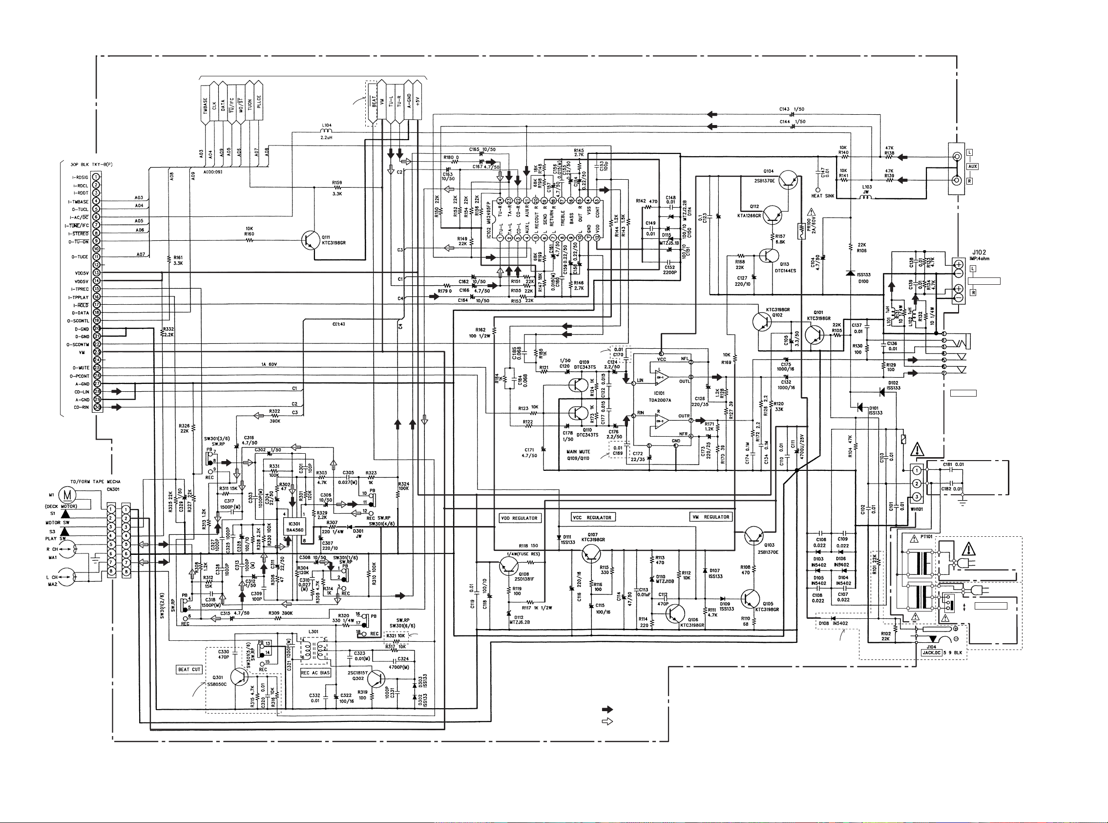
SCHEMATIC DIAGRAM-1 (MAIN 1/2)
TO FRONT C.B CN201
MAIN C.B
(1/2)
J105
TO MAIN C.B 2/2
INV.
HS
HS
IC102
FUNCTION
SWITCH
POWER AMP
REG
C121
137 MODEL:330/25V
157 MODEL:470/35V
REG
HOLD DET
J101
JACK. PIN 3P MSP
R
SW
HOLD DET
SPEAKERS
IC301
CASSETTE
PER AMP
HS
137 MODEL:1K
157 MODEL:820
137 MODEL:1K
157 MODEL:820
REG
HS
REG
POWER
CONT
REG
POWER
ON/OFF
HS
F101
3.15A 250V
PT101
J101
JACK. 3.5 ST
PHONES
(1/2)
AC C.B(2/2)
120V
220-240V
SW1
AC C.B
HS,VJ
230V
50Hz
120/220-240V
50/60Hz
AC VOLTAGE
AC C.B
(2/2)
HR,HC,HA,HT
HS
BEAT CUT
BIAS OSC
SIGNAL
: PB/FM
: REC/AM
1413
Page 3
IC BLOCK DIAGRAM
IC, M62495AFP
IC, LA6541D
AUTO RESET
IC, LA1837NL IC, LC72131D
1615
Page 4
SCHEMATIC DIAGRAM-2 (MAIN: EXCEPT HS 2/2)
MAIN C.B (2/2)
TUNER
ON/OFF
SWITCH
DC BALANCE
ADJ
AM IF ADJ
IF AMP
R
BAND SW
*2
*1
FM FRONTEND
PACK
*2
1
2
3
4
FM 75Ω
ANTENNA
AM LOOP
TO MAIN C.B (1/2)
1500P
1500P
IC771
FM/AM IF/STEREO
TUNER SYSTEM
L981(2/2)
*2
VJ 100
AM TRACKING
R821 R822
NO
MOUNTED
180OTHERS
10K
ADJ
*1
VJ 6ZA-1
OTHERS FEUNC
L981(1/2)
FEE801
YFEVNC
8ZA-1
SIGNAL
: PB/FM
: REC/AM
1817
Page 5

SCHEMATIC DIAGRAM-3 (MAIN: HS 2/2)
TO MAIN C.B (1/2)
MAIN C.B (2/2)
BEAT
VM
+5V
TUNER
ON//OFF
SWITCH
1SS133
2.2µH
DC BALANCE
ADJ
AM IF ADJ
IC771
FM/AM IF/STEREO
TUNER SYSTEM
FM IF
BAND
SW
R
MW/LW SW
R
J801
ANTENNA
FM 75Ω
MW/LW
LOOP
AM RF AMP
L773
D944
D942
0.015
0.015
LW OSC SW
LW ANT SW
SIGNAL
: PB/FM
: REC/AM
2019
Page 6

SCHEMATIC DIAGRAM-4 (FRONT)
VJ
HS
HA
2625
Page 7

SCHEMATIC DIAGRAM-5 (CD)
2827
Page 8

IC DESCRIPTION
IC, LC867240A-5P15
Pin No. Pin Name I/O Description
1
2
3
4
5
6
7
8
9
10
11
12
13
O-SCONTM
O-SCONTL
O-DATA
___________
I-TUNE/IFC
O-TUCL
O-COIN
I-SQOUT
___________
O-CQCK
O-RWC
_______________
O-CLKSFT
I-TMBASE
____________
I-RESET
XT1
O
M62439SP control. open drain output.
O
O
Tuner control. CMOS output.
I
Tuner control.
O
Tuner control. CMOS output.
O
CD control. open drain output.
I
CD control.
O
CD control. open drain output.
O
O
Clock shift output. “L” during shift. open drain output.
I
8 Hz time base input.
I
Reset input.
I
Input pin.
14
15
16, 17
18
19
20
21
22
23
24
25
26
27
28
29
30
31
32
33
XT2
VSS1
CF1, CF2
VDD1
I-KEY0
I-KEY1
I-RDSIG
I-WRQ
I-DRF
I-DOOR
I-PUIN
I-SWTAPE
________________
I-STEREO
I-RDCL
________
I-REM
___________
I-HOLD
I-RDDT
I-TPREC
I-TPPLAY
O
—
I/O
—
Output pin for 32.768kHz crystal oscillation.
GND.
Main clock input/output 5.76 MHz.
+5V.
I
KEY0 A/D input.
I
KEY1 A/D input.
I
RDS signal level input. (A/D input)
I
CD control.
I
I
CD door SW detection SW input. “L” at CLOSE.
I
CD pick-up detection SW input. “L” at ON.
I
Tape detection SW input. (A/D input)
I
Monaural/stereo indication selector input. “L” at stereo.
I
RDS clock input.
I
Remote control input. (fall-down edge interrupt input)
I
Hold mode detection. “L” at hold mode.
I
RDS data input.
I
Tape REC detection input. “H” at REC.
I
Tape PLAY detection input. “H” at PLAY.
34
35
36-38
39-55
56
57
58-79
80
81
O-MOTOR
O-PL
O-NC
S9-S25
VDD2
VSS2
S26-S47
I-CLKDSP
I-AS
—
—
O
Mechanism deck motor ON/OFF output. “H” at ON. CMOS output.
O
Mechanism deck plunger solenoid ON/OFF output. “H” at ON. CMOS output .
O
Not used.
O
LCD SEG terminal Initial setting output. (S10 to S16)
+5V.
GND.
O
LCD SEG terminal .
I
Watch indication select input “L”: 12H. “H”: 24H.
I
Auto stop. counter input .
39
Page 9
Pin No. Pin Name I/O Description
__________
82
83-86
87
88
89
90
91
92
I-STOP
COM0-COM3
I-INIT
______
I-AC/DC
VSS3
VDD3
O-NC
O-TUCE
—
—
I
Tape stop input.
O
LCD common output.
I
Initial setting input.
O
Beat selector output. “H” during selection. CMOS output .
GND.
5V.
O
Not used.
O
Tuner chip enable output. CMOS output .
93
94
95
96
97
98
99
100
O-CD-ON
_____________
O-TU-ON
__________
O-RMT
________ _____
O-REC/PB
O-MUTE
O-PCONT
__________
O-BIAS
O-NC
O
“H” output during CD function. CMOS output.
O
“H” output during TU function. Open drain output.
O
REC mute output. “H” during mute. Open drain output.
O
REC/PB select output. “H” during PB. Open drain output.
O
Mute output. “H” during mute. Open drain output.
O
Power control output. “H” at ON. CMOS output.
O
REC bias ON/OFF output. “H” at ON. Open drain output.
O
Not used.
40
Page 10

IC, LA9241ML
Pin No. Pin Name I/O Description
1
2
FIN2
FIN1
Pin to which external pickup photo diode is connected. RF signal is created by adding
I
with the FIN1 pin signal. FE signal is created by subtracting from the FIN1 pin signal.
I
Pin to which external pickup photo diode is connected.
10
11
12
13
14
15
16
17
3
4
5
6
7
8
9
E
F
TB
TE–
TE
TESI
SCI
TH
TA
TD–
TD
JP
TO
FD
FD–
Pin to which external pickup photo diode is connected. TE signal is created by
I
subtracting from the F pin signal.
I
Pin to which external pickup photo diode is connected.
I
DC component of the TE signal is input.
I
Pin to which external resistor setting the TE signal gain is connected between the TE pin.
O
TE signal output pin.
TES “Track Error Sense” comparator input pin. TE signal is passed through a band-
I
pass filter then input.
I
Shock detection signal input pin.
I
Tracking gain time constant setting pin.
O
TA amplifier output pin.
Pin to which external tracking phase compensation constants are connected between
I
the TD and VR pins.
I
Tracking phase compensation setting pin.
I
Tracking jump signal (kick pulse) amplitude setting pin.
O
Tracking control signal output pin.
O
Focusing control signal output pin.
Pin to which external focusing phase compensation constants are connected between
I
the FD and FA pins.
18
19
20
21
22
23
24
25
26
27
28
29
30, 31
32, 33
34
FA
FA–
FE
FE–
AGND
SP
SPI
SPG
SP–
SPD
SLEQ
SLD
SL–, SL+
JP–, JP+
TGL
—
—
Pin to which external focusing phase compensation constants are connected between
I
the FD– and FA– pins.
Pin to which external focusing phase compensation constants are connected between
I
the FA and FE pins.
O
FE signal output pin.
I
Pin to which external FE signal gain setting resistor is connected between the FE pin.
Analog signal GND.
Single ended output of the CV+ and CV– pin input signal.
I
Spindle amp input.
I
Pin to which external spindle gain setting resistor in 12 cm mode is connected.
Pin to which external spindle phase compensation constants are connected together
I
with SPD pin.
O
Spindle control signal output pin.
I
Pin to which external sled phase compensation constants are connected.
O
Sled control signal output pin.
I
Sled advance signal input pin from microprocessor.
I
Tracking jump signal input pin from DSP.
I
Tracking gain control signal input from DSP. Low gain when TGL = H.
35
TOFF
I
Tracking off control signal input pin from DSP. Off when TOFF = H.
41
Page 11

Pin No. Pin Name I/O Description
36
TES
O
Pin from which TES signal is output to DSP.
37
38
39, 40
41
42
43
44
45
46
47
48
49
50
51
52
53
54
55
HFL
SLOF
CV–, CV+
RFSM
RFS–
SLC
SLI
DGND
FSC
TBC
NC
DEF
CLK
CL
DAT
CE
DRF
FSS
—
—
“High Frequency Level” is used to judge whether the main beam position is on top of
O
bit or on top of mirror.
I
Sled servo off control input pin.
I
CLV error signal input pin from DSP.
O
RF output pin.
RF gain setting and EFM signal 3T compensation constant setting pin together with
I
RFSM pin.
“Slice Level Control” is the output pin which controls the RF signal data slice level by
O
DSP.
I
Input pin which control the data slice level by the DSP.
Digital system GND.
O
Output pin to which external focus search smoothing capacitor is connected.
I
“Tracking Balance Control” EF balance variable range setting pin.
No connection.
O
Disc defect detector output pin.
I
Reference clock input pin. 4.23 MHz of the DSP is input.
I
Microprocessor command clock input pin.
I
Microprocessor command data input pin.
I
Microprocessor command chip enable input pin.
O
“Detect RF” RF level detector output.
I
“Focus Search Select” focus search mode (± search/+ search) select pin.
56
57
58
59
60
61
62
63
64
VCC2
REFI
VR
LF2
PH1
BH1
LDD
LDS
VCC1
—
—
—
Servo system and digital system Vcc pin.
Pin to which external bypass capacitor for reference voltage is connected.
O
Reference voltage output pin.
I
Disc defect detector time constant setting pin.
I
Pin to which external capacitor for RF signal peak holding is connected.
I
Pin to which external capacitor for RF signal bottom holding is connected.
O
APC circuit output pin.
I
APC circuit input pin.
RF system Vcc pin.
42
Page 12

IC, LC78622ED
Pin No. Pin Name I/O Description
1
2
3
4
DEFI
TAI
PDO
VVSS
—
I
Defect sense signal (DEF) input pin. (Connect to 0V when not used).
I
O
Test signal input pin with built-in pull-down resistor. Be sure to connect to 0V.
Phase comparator output pin to control external VCO.
GND pin for built-in VCO. Be sure to connect to 0V.
For PLL.
5
6
7
8
9
ISET
VVDD
FR
VSS
EFMO
—
—
I
Pin to which external resistor adjusting the PD0 output current.
Power supply pin for built-in VCO.
I
Pin for VCO frequency range adjustment.
Digital system GND. Be sure to connect to 0V.
O
EFM signal output pin.
For slice level control.
10
11
12, 13
14
EFMIN
TEST2
CLV+, CLV–
___
V/P
I
I
Test signal input pin with built-in pull-down resistor. Be sure to connect to 0V.
O
Disc motor control output. Three level output is possible using command.
Rough servo or phase control automatic selection monitoring output pin. Rough servo
O
EFM signal input pin.
at H. Phase servo at L.
15
16
17
18
19, 20
21
22
HFL
TES
TOFF
TGL
JP+, JP–
PCK
FSEQ
I
Track detect signal input pin. Schmidt input.
I
Tracking error signal input pin. Schmidt input.
O
Tracking OFF output pin.
O
Tracking gain selection output pin. Gain boost at L.
O
Track jump control signal output pin. Three level output is possible using command.
O
EFM data playback clock monitoring pin 4.3218 MHz when phase is locked in.
Sync signal detection output pin. H when the sync signal which is detected from EFM
O
signal and thesync signal which is internally generated agree.
23
VDD
—
Digital system power supply pin.
The pin is controlled by the serial data
command from microprocessor. When
24-28
SL+, SL–, CONT3-5
I/O
General purpose input/output pin 1 to 5.
the pin is not used, set the pin to the input
terminal and connect to 0V, or alternately
set the pin to output terminal and leave
the pin open.
29
EMPH
O
De-emphasis monitor output pin. De-emphasis disc is being played back at H.
Pin No. Pin Name I/O Description
43
44
45
46
47
48
49
50
XVDD
XOUT
XIN
XVSS
SBSY
EFLG
PW
SFSY
—
—
Crystal oscillator power supply pin.
O
Pin to which external 16.9344 MHz crystal oscillator is connected.
I
Crystal oscillator GND pin. Be sure to connect to 0V.
O
Subcode block sync signal output pin.
O
C1, C2, single and dual correction monitoring pin.
O
Subcode P, Q, R, S, T, U and W output pin.
O
Subcode frame sync signal output pin. Falls down when subcode enters standby.
Subcode read clock input pin. Schmidt input. (Be sure to connected to 0V when not
51
SBCK
I
in use.)
52
FSX
Pin outputting the 7.35 kHz sync signal which is generated by dividing frequency of
O
crystal oscillator.
53
54
55
56
57
58
59
60
61
62
63
WRQ
RWC
SQOUT
COIN
___________
CQCK
________
RES
TST11
16M
4.2M
TEST5
______
CS
O
Subcode Q output standby output pin.
I
Read/write control input pin. Schmidt input.
O
Subcode Q output pin.
I
Command input pin from microprocessor.
I
Command input read clock or subcode read input clock from SQOUT pin
I
LC78622 reset input pin. Set this pin to L once when the main power is turned on.
O
Test signal output pin. Use this pin as open (normally L output).
O
16.9344 MHz output pin.
O
4.2336 MHz output pin.
I
Test signal input pin with built-in pull-down resistor. Be sure to connect to 0V.
Chip select signal input pin with built-in pull-down resistor. Be sure to connect to 0V
I
while it is not controlling.
64
TEST1
I
Test signal input pin without built-in pull-down resistor. Be sure to connect to 0V.
Note: The same potential must be applied to the respective power supply terminals. (VDD, VVDD, LVDD, RVDD, XVDD)
30
31
32, 33
34
35
36
37
38
39
40
41
42
C2F
DOUT
TEST3, TEST4
N.C.
MUTEL
LVDD
LCHO
LVSS
RVSS
RCHO
RVDD
MUTER
—
—
—
—
—
O
C2 flag output pin.
O
DIGITAL OUT output pin. (EIAJ format).
I
Test signal input pin with built-in pull-down resistor. Be sure to connect to 0V.
Not used. Set the pin to open.
O
L-channel 1-bit DAC.
O
L-channel mute output pin.
L-channel power supply pin.
L-channel output pin.
L-channel GND. Be sure to connect to 0V.
R-channel GND. Be sure to connect to 0V.
O
R-channel output pin.
R-channel 1-bit DAC.
R-channel power supply pin.
O
R-channel mute output pin.
4443
 Loading...