

Page 1
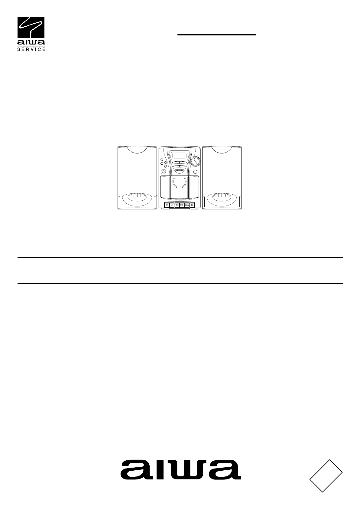
LCX-107
EZ(S) EZ(L)
K(S) HS(S)
HRJ(S)
SERVICE MANUAL
COMPACT DISC STEREO
SYSTEM
BASIC TAPE MECHANISM : ZZM-1AR3NC
BASIC CD MECHANISM : DA11T3C
S/M Code No. 09-00A-350-1N1
DATA
Page 2
SPECIFICATIONS
HR MODEL K, EZ, HS MODELS
Design and specifications are subject to change without
•
notice
.
ACCESSORIES/PACKAGE LIST
REF. NO PART NO. KANRI DESCRIPTION
1 8A-CLD-906-010 IB,EZ(9L)FM<EZS,EZL>
1 8A-CLD-901-010 IB,H(ECA)FM<HRS>
1 8A-CLD-905-010 IB,K(E)FM<KS>
2 87-A90-030-010 ANT,LOOP AM-NC C
3 87-A90-118-010 ANT,WIRE FM (Z)<EXCEPT HRS>
NO.
Design and specifications are subject to change without
•
notice
.
REF. NO PART NO. KANRI DESCRIPTION
3 87-A90-064-010 FEEDER-ANT,FM(SHS)<HRS>
!
4 87-099-726-010 PLUG,ADPTR CONV(K)<KS>
!
4 87-A91-017-010 PLUG,CONVERSION JT-0476<HRS>
5 8A-CLB-961-010 RC UNIT,RC-AAT11
NO.
-2-
Page 3
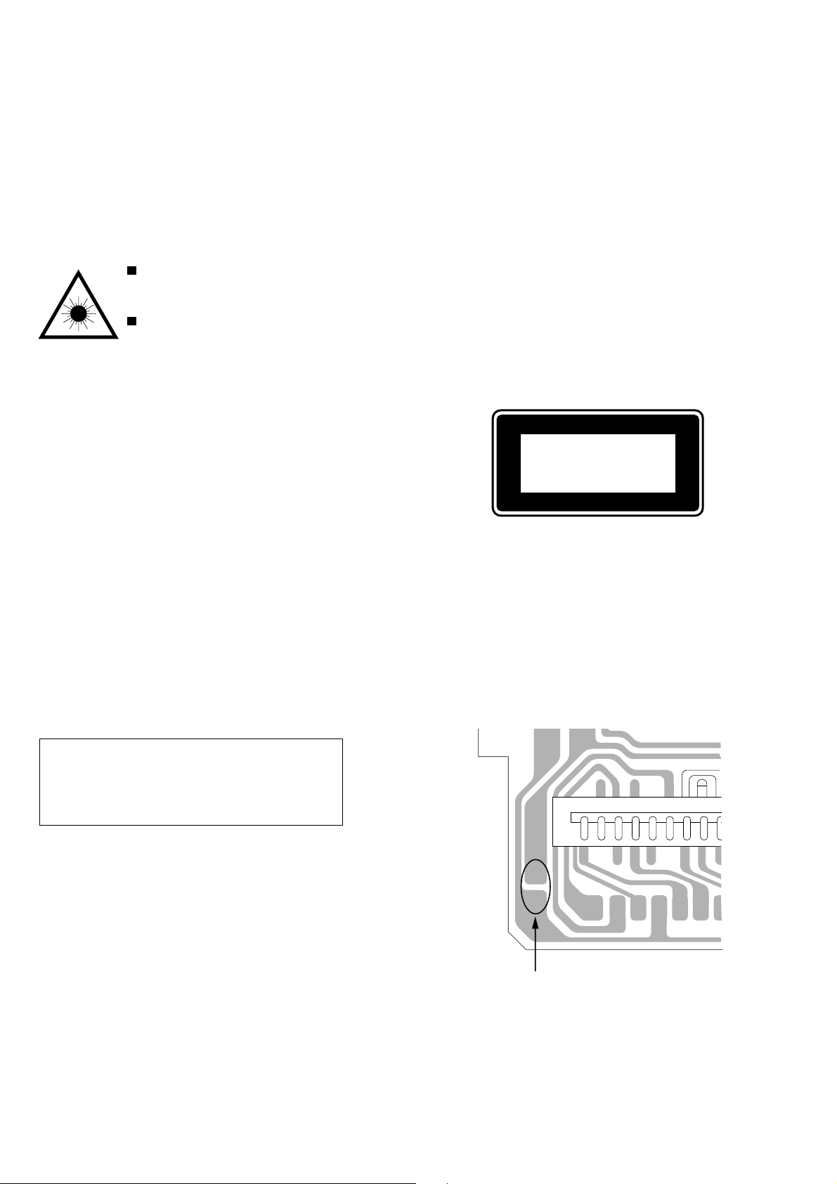
PROTECTION OF EYES FROM LASER BEAM DURING SERVICING
This set employs laser. Therefore, be sure to follow carefully the
instructions below when servicing.
WARNING!
WHEN SERVICING, DO NOT APPROACH THE LASER EXIT
WITH THE EYE TOO CLOSELY. IN CASE IT IS NECESSARY TO
CONFIRM LASER BEAM EMISSION. BE SURE TO OBSERVE
FROM A DISTANCE OF MORE THAN 30cm FROM THE
SURFACE OF THE OBJECTIVE LENS ON THE OPTICAL
PICK-UP BLOCK.
Caution: Invisible laser radiation when
open and interlocks defeated avoid exposure to beam.
Advarsel:Usynling laserståling ved åbning,
når sikkerhedsafbrydere er ude af funktion.
Undgå udsættelse for stråling.
VAROITUS!
Laiteen Käyttäminen muulla kuin tässä käyttöohjeessa mainitulla tavalla saattaa altistaa käyt-täjän turvallisuusluokan 1 ylittävälle näkymättömälle lasersäteilylle.
VARNING!
Om apparaten används på annat sätt än vad som specificeras i
denna bruksanvising, kan användaren utsättas för osynling
laserstrålning, som överskrider gränsen för laserklass 1.
CAUTION
Use of controls or adjustments or performance of procedures
other than those specified herein may result in hazardous
radiation exposure.
ATTENTION
L'utilisation de commandes, réglages ou procédures autres que
ceux spécifiés peut entraîner une dangereuse exposition aux
radiations.
ADVARSEL!
Usynlig laserståling ved åbning, når sikkerhedsafbrydereer ude
af funktion. Undgå udsættelse for stråling.
This Compact Disc player is classified as a CLASS 1 LASER
product.
The CLASS 1 LASER PRODUCT label is located on the rear
exterior.
CLASS 1
KLASSE 1
LUOKAN 1
KLASS 1
LASER PRODUCT
LASER PRODUKT
LASER LAITE
LASER APPARAT
Precaution to replace Optical block
(SF-P101NR)
Body or clothes electrostatic potential could ruin
laser diode in the optical block. Be sure ground
body and workbench, and use care the clothes
do not touch the diode.
1) After the connection, remove solder shown in
the right figure.
PICK-UP Assy P.C.B
Solder
-3-
Page 4

ELECTRICAL MAIN PARTS LIST
REF. NO PART NO. KANRI DESCRIPTION
NO.
IC
87-A21-064-010 IC,LA4227
87-A21-443-040 C-IC,M62495AFP
87-A20-446-010 C-IC,LA9241ML
87-A20-459-010 C-IC,LC78622ED
87-A21-093-010 IC,LA6541D
87-A21-431-010 IC,BA4560N
8A-CLD-630-010 C-IC,LC867132V-5S27
87-A20-650-010 IC,RPM6938-V11
87-070-127-110 IC,LC72131 D
87-A20-913-010 IC,LA1837NL
TRANSISTOR
89-318-154-080 TR,2SC1815 (0.4W)
87-026-463-080 TR,2SA933S (0.3W)
89-112-965-080 TR,2SA1296 (0.75W)
87-026-291-080 TR,DTC124XS
89-213-702-010 TR,2SB1370 (1.8W)
87-026-462-080 TR,2SC1740 S(RS 0.3W)
87-026-215-080 TR,DTC114YS
87-026-290-080 TR,DTA124X
89-109-332-380 TR,2SA933RS
89-113-187-080 TR,2SA1318TU
87-026-239-080 TR,DTC114TK (0.2W)
87-026-213-080 CHIP-TR,DTC114YK
87-026-464-080 TR,DTC114TS (0.3W)
87-A30-072-080 C-TR,RT1P 144C
89-327-143-080 TR,2SC2714 (0.1W)
89-505-434-540 C-FET,2SK543(4/5)<EXCEPT HRS>
87-A30-086-070 C-TR,CSD1306E<EXCEPT HRS>
87-A30-074-080 C-TR,RT1P 141C<EXCEPT HRS>
DIODE
87-070-345-080 DIODE,IN4148
87-017-978-080 DIODE,1N4003
87-020-465-080 DIODE,1SS133 (110MA)
87-A40-345-080 ZENER,MTZJ10C
87-A40-648-080 ZENER,MTZJ8.2A
87-027-702-080 DIODE,ZENER HZ6C2L (200MA)
87-A40-234-080 ZENER,MTZJ5.6A
87-017-149-080 ZENER,HZS6A2L
87-A40-465-010 DIODE,FR202
87-A40-442-080 ZENER,MTZJ9.1A
87-A40-498-080 ZENER,MTZJ24B<HRS>
87-A40-270-080 C-DIODE,MC2838<EXCEPT HRS>
MAIN C.B
C211 87-010-401-080 CAP, ELECT 1-50V
C212 87-010-401-080 CAP, ELECT 1-50V
C237 87-010-371-080 CAP, ELECT 470-6.3V
C239 87-010-401-080 CAP, ELECT 1-50V
C240 87-010-401-080 CAP, ELECT 1-50V
C247 87-010-401-080 CAP, ELECT 1-50V
C248 87-010-401-080 CAP, ELECT 1-50V
C251 87-010-404-080 CAP, ELECT 4.7-50V
C257 87-010-401-080 CAP, ELECT 1-50V
C258 87-010-401-080 CAP, ELECT 1-50V
C261 87-010-401-080 CAP, ELECT 1-50V
C262 87-010-401-080 CAP, ELECT 1-50V
C263 87-012-286-080 CAP, U 0.01-25<KS,EZS,EZL>
C263 87-012-274-080 CHIP CAP,U 1000P-50B<HRS,HSS>
C264 87-012-286-080 CAP, U 0.01-25<KS,EZS,EZL>
C264 87-012-274-080 CHIP CAP,U 1000P-50B<HRS,HSS>
C265 87-010-263-080 CAP, ELECT 100-10V
C266 87-010-263-080 CAP, ELECT 100-10V
C267 87-010-112-080 CAP, ELECT 100-16V
C268 87-010-112-080 CAP, ELECT 100-16V
REF. NO PART NO. KANRI DESCRIPTION
NO.
C271 87-010-221-080 CAP, ELECT 470-10V
C272 87-010-221-080 CAP, ELECT 470-10V
C278 87-010-405-080 CAP, ELECT 10-50V
C279 87-010-385-080 CAP, ELECT 220-25V
C280 87-010-196-080 CHIP CAPACITOR,0.1-25
C281 87-010-196-080 CHIP CAPACITOR,0.1-25
C291 87-012-286-080 CAP, U 0.01-25
C292 87-012-286-080 CAP, U 0.01-25<HRS,HSS>
C292 87-018-134-080 CAPACITOR,TC-U 0.01-16<KS,EZS,EZL>
C293 87-012-286-080 CAP, U 0.01-25
C294 87-012-286-080 CAP, U 0.01-25
C295 87-018-127-080 CAP, CER 470P-50V<KS,EZS,EZL>
C296 87-018-127-080 CAP, CER 470P-50V<KS,EZS,EZL>
C297 87-A11-154-080 CAP,TC U 4700P-16 Z F<KS,EZS,EZL>
C298 87-A11-154-080 CAP,TC U 4700P-16 Z F<KS,EZS,EZL>
C301 87-016-495-000 CAP,E 3300-25 M SMG
C306 87-010-404-080 CAP, ELECT 4.7-50V
C307 87-010-401-080 CAP, ELECT 1-50V
C308 87-010-221-080 CAP, ELECT 470-10V
C310 87-010-248-080 CAP, ELECT 220-10V
C311 87-010-263-080 CAP, ELECT 100-10V
C312 87-010-385-080 CAP, ELECT 220-25V
C316 87-010-263-080 CAP, ELECT 100-10V
C317 87-A11-145-080 CAP,TC U 0.01-50 Z F
C331 87-010-401-080 CAP, ELECT 1-50V
C332 87-010-384-080 CAP, ELECT 100-25V
C333 87-A11-148-080 CAP,TC U 0.1-50 Z F
C334 87-010-404-080 CAP, ELECT 4.7-50V
C335 87-018-119-080 CAP, CER 100P-50V<HRS>
C701 87-010-381-080 CAP, ELECT 330-16V
C702 87-010-404-080 CAP, ELECT 4.7-50V
C703 87-012-286-080 CAP, U 0.01-25
C704 87-012-286-080 CAP, U 0.01-25
C705 87-A10-592-080 C-CAP,S 0.015-50 J B<HRS>
C706 87-A10-592-080 C-CAP,S 0.015-50 J B<HRS>
C709 87-012-195-080 C-CAP,U 100P-50CH
C713 87-012-286-080 CAP, U 0.01-25<EXCEPT HRS>
C714 87-012-286-080 CAP, U 0.01-25
C715 87-012-195-080 C-CAP,U 100P-50CH<EXCEPT HRS>
C717 87-012-286-080 CAP, U 0.01-25
C719 87-012-286-080 CAP, U 0.01-25
C720 87-012-195-080 C-CAP,U 100P-50CH
C721 87-012-176-080 CAP 15P
C722 87-012-176-080 CAP 15P
C723 87-012-274-080 CHIP CAP,U 1000P-50B
C725 87-018-131-080 CAP, CER 1000P-50V<EXCEPT HRS>
C725 87-012-274-080 CHIP CAP,U 1000P-50B<HRS>
C727 87-010-196-080 CHIP CAPACITOR,0.1-25
C728 87-010-260-080 CAP, ELECT 47-25V
C729 87-012-274-080 CHIP CAP,U 1000P-50B
C731 87-012-286-080 CAP, U 0.01-25
C733 87-010-987-080 C-CAP,S 1500P-50 CH<HRS>
C733 87-012-280-080 CAP, U 3300P-50<EXCEPT HRS>
C734 87-010-987-080 C-CAP,S 1500P-50 CH<HRS>
C734 87-012-280-080 CAP, U 3300P-50<EXCEPT HRS>
C735 87-010-987-080 C-CAP,S 1500P-50 CH<HRS>
C736 87-010-987-080 C-CAP,S 1500P-50 CH<HRS>
C737 87-A10-592-080 C-CAP,S 0.015-50 J B<HRS>
C738 87-A10-592-080 C-CAP,S 0.015-50 J B<HRS>
C751 87-010-220-080 C-CAP,S 0.018-25 B<HRS>
C752 87-010-220-080 C-CAP,S 0.018-25 B<HRS>
C752 87-012-282-080 CAP, U 4700P-50<EXCEPT HRS>
C753 87-012-195-080 C-CAP,U 100P-50CH<EXCEPT HRS>
C755 87-012-286-080 CAP, U 0.01-25<EXCEPT HRS>
C756 87-012-286-080 CAP, U 0.01-25
C757 87-012-188-080 C-CAP,U 47P-50 CH
C758 87-012-167-080 C-CAP,U 5P-50 CH
C761 87-010-196-080 CHIP CAPACITOR,0.1-25<EXCEPT HRS>
C762 87-012-286-080 CAP, U 0.01-25<EXCEPT HRS>
C763 87-010-829-080 CAP, U 0.047-16
-4-
Page 5

REF. NO PART NO. KANRI DESCRIPTION
NO.
C764 87-012-337-080 C-CAP,U 56P-50 CH<HRS>
C764 87-012-271-080 CAP, U 560P-50<KS,EZS,EZL>
C765 87-012-286-080 CAP, U 0.01-25
C766 87-010-197-080 CAP, CHIP 0.01 DM<EXCEPT HRS>
C768 87-012-286-080 CAP, U 0.01-25
C769 87-010-260-080 CAP, ELECT 47-25V
C770 87-010-829-080 CAP, U 0.047-16
C771 87-010-383-080 CAP, ELECT 33-25V
C772 87-010-829-080 CAP, U 0.047-16
C773 87-010-196-080 CHIP CAPACITOR,0.1-25
C774 87-010-263-080 CAP, ELECT 100-10V
C775 87-010-404-080 CAP, ELECT 4.7-50V
C776 87-012-286-080 CAP, U 0.01-25
C777 87-010-400-080 CAP, ELECT 0.47-50V<HRS>
C777 87-010-493-080 CAP,E 0.47-50 GAS<EXCEPT HRS>
C778 87-010-401-080 CAP, ELECT 1-50V
C779 87-010-401-080 CAP, ELECT 1-50V
C780 87-010-196-080 CHIP CAPACITOR,0.1-25
C781 87-010-405-080 CAP, ELECT 10-50V
C782 87-010-405-080 CAP, ELECT 10-50V
C783 87-012-286-080 CAP, U 0.01-25
C784 87-012-286-080 CAP, U 0.01-25
C785 87-010-401-080 CAP, ELECT 1-50V<HRS>
C785 87-010-402-080 CAP, ELECT 2.2-50V<EXCEPT HRS>
C786 87-010-401-080 CAP, ELECT 1-50V<HRS>
C786 87-010-402-080 CAP, ELECT 2.2-50V<EXCEPT HRS>
C787 87-012-275-080 C-CAP,U 1200P-50 B<EXCEPT HRS>
C788 87-012-275-080 C-CAP,U 1200P-50 B<EXCEPT HRS>
C789 87-012-275-080 C-CAP,U 1200P-50 B
C790 87-012-275-080 C-CAP,U 1200P-50 B
C791 87-010-405-080 CAP, ELECT 10-50V
C793 87-012-273-080 C-CAP,U 820P-50 B
C794 87-010-406-080 CAP, ELECT 22-50
C795 87-010-596-080 CAP, S 0.047-16
C796 87-010-403-080 CAP, ELECT 3.3-50V
C797 87-012-276-080 CAP, CHIP SS 1500 PBK<EXCEPT HRS>
C798 87-012-276-080 CAP, CHIP SS 1500 PBK<EXCEPT HRS>
C799 87-010-829-080 CAP, U 0.047-16
C812 87-012-286-080 CAP, U 0.01-25
C814 87-012-286-080 CAP, U 0.01-25<EXCEPT HRS>
C820 87-010-260-080 CAP, ELECT 47-25V
C821 87-012-286-080 CAP, U 0.01-25
C822 87-012-286-080 CAP, U 0.01-25
C823 87-012-286-080 CAP, U 0.01-25
C828 87-010-196-080 CHIP CAPACITOR,0.1-25
C829 87-010-196-080 CHIP CAPACITOR,0.1-25
C830 87-010-265-080 CAP, ELECT 33-16V<EXCEPT HRS>
C940 87-012-286-080 CAP, U 0.01-25<EXCEPT HRS>
C942 87-012-168-080 C-CAP,U 6P-50 CH<EXCEPT HRS>
C947 87-012-286-080 CAP, U 0.01-25<EXCEPT HRS>
C949 87-A10-039-080 C-CAP,U 470P-50 J CH<EXCEPT HRS>
C952 87-012-286-080 CAP, U 0.01-25<EXCEPT HRS>
C958 87-010-197-080 CAP, CHIP 0.01 DM<EXCEPT HRS>
C959 87-010-831-080 C-CAP,U,0.1-16F<EXCEPT HRS>
C959 87-010-196-080 CHIP CAPACITOR,0.1-25<HRS>
C960 87-010-196-080 CHIP CAPACITOR,0.1-25
C961 87-012-170-080 C-CAP,U 8P-50 CH<HRS>
C962 87-010-401-080 CAP, ELECT 1-50V<EXCEPT HRS>
C963 87-010-196-080 CHIP CAPACITOR,0.1-25<HRS>
C999 87-A11-155-080 CAP,TC U 0.01-16 Z F<KS,EZS,EZL>
CF801 87-008-423-010 CERAMIC FILTER, SFE10.7<EXCEPT HRS>
CF801 87-008-261-010 FILTER, SFE10.7MA5-A<HRS>
CF802 82-785-747-010 CF MS2 GHY R<EXCEPT HRS>
CF802 87-008-261-010 FILTER, SFE10.7MA5-A<HRS>
CN201 87-099-014-010 CONN,12P 6216 V
CN202 87-099-569-010 CONN,12P TUC-P12P-B1
CN301 87-099-043-010 CONN 2P EH
FFE801 A8-6ZA-19C-170 6ZA-1 YFEENC<EXCEPT HRS>
FFE801 A8-8ZA-193-070 8ZA-1 YFEUNC<HRS>
J201 87-A60-420-010 JACK,3.5 ST (MSC)
REF. NO PART NO. KANRI DESCRIPTION
J202 87-A60-659-010 TERMINAL,SPKR 4P HSP-134V-05Z
J203 87-A60-881-010 JACK,PIN 2P MSP 242V05 PBSN
J801 87-A60-702-010 TERMINAL,ANT 4P CJ-9036<HRS>
J801 87-033-241-010 TERMINAL,ANT AJ-2039<EXCEPT HRS>
JR11 87-012-286-080 CAP, U 0.01-25<KS,EZS,EZL>
L201 87-005-366-010 COIL, 1UH
L202 87-005-366-010 COIL, 1UH
L301 87-003-098-080 COIL,2.2UH<HRS>
L302 87-008-372-080 FILTER, EMI BL OIRNI<KS,EZS,EZL>
L771 87-A50-266-010 COIL,FM DET-2N(TOK)
L772 87-A91-110-010 FLTR,PCFJZH-450 (TOK)
L781 87-005-847-080 COIL,2.2UH(CECS)<EXCEPT HRS>
L832 87-005-847-080 COIL,2.2UH(CECS)<EXCEPT HRS>
L941 87-A50-020-010 COIL,ANT LW(COI)<EXCEPT HRS>
L942 87-A50-019-010 COIL,OSC LW(COI)<EXCEPT HRS>
L981 8Z-ZA1-665-010 COIL,AM PACK 2(TOK)<EXCEPT HRS>
L981 8Z-ZA1-667-010 COIL,AM PACK 4F(TOK)<HRS>
TC942 87-A91-658-010 TRIMMER,30P 4.0X4.5 ECRL<EXCEPT HRS>
X721 87-A70-061-010 VIB,XTAL 4.500MHZ CSA-309
FR C.B
C601 87-012-178-080 C-CAP,U 18P-50 CH
C602 87-012-182-080 C-CAP,U 27P-50 CH
C603 87-012-337-080 C-CAP,U 56P-50 CH
C604 87-012-176-080 CAP 15P
C605 87-012-186-080 C-CAP,U 39P-50 CH
C607 87-A11-148-080 CAP,TC U 0.1-50 Z F
C608 87-010-831-080 C-CAP,U,0.1-16F
C610 87-010-248-080 CAP, ELECT 220-10V
C611 87-A11-148-080 CAP,TC U 0.1-50 Z F
C612 87-010-248-080 CAP, ELECT 220-10V
C613 87-010-402-080 CAP, ELECT 2.2-50V
C614 87-A11-148-080 CAP,TC U 0.1-50 Z F
C615 87-010-400-080 CAP, ELECT 0.47-50V
C616 87-010-401-080 CAP, ELECT 1-50V
C617 87-A11-112-080 CAP,TC U 1000P-50 J CH
C618 87-010-560-040 CAP,E 10-50 GAS
C620 87-015-785-080 CHIP CAPACITOR, 0.1FZ-25Z
C627 87-A10-826-080 C-CAP,S 1-10 K B
C628 87-010-263-080 CAP, ELECT 100-10V
C630 87-A11-148-080 CAP,TC U 0.1-50 Z F
C631 87-010-831-080 C-CAP,U,0.1-16F
C633 87-012-286-080 CAP, U 0.01-25
C634 87-012-286-080 CAP, U 0.01-25
C635 87-012-286-080 CAP, U 0.01-25
CN601 87-099-029-010 CONN,12P 6216H
CNA602 8A-CLD-623-010 CONN ASSY,2P LED
L601 87-003-171-010 COIL,15UH TROIDAL
L603 87-003-171-010 COIL,15UH TROIDAL
LCD601 8A-CLD-610-010 LCD,AIW4239ACL-13
LED609 87-A40-626-010 LED,L-934ID RED
S601 87-A91-704-080 SW,TACT EVQ 214 05R
S602 87-A91-704-080 SW,TACT EVQ 214 05R
S603 87-A91-704-080 SW,TACT EVQ 214 05R
S604 87-A91-704-080 SW,TACT EVQ 214 05R
S605 87-A91-704-080 SW,TACT EVQ 214 05R
S608 87-A91-704-080 SW,TACT EVQ 214 05R
S609 87-A91-704-080 SW,TACT EVQ 214 05R
S610 87-A91-704-080 SW,TACT EVQ 214 05R
S611 87-A91-704-080 SW,TACT EVQ 214 05R
S612 87-A91-704-080 SW,TACT EVQ 214 05R
S613 87-A91-704-080 SW,TACT EVQ 214 05R
S614 87-A91-704-080 SW,TACT EVQ 214 05R
X601 87-030-273-010 VIB,XTAL 32.768K5PPM
X602 87-030-376-080 VIB,CER CSA5.76MG200
CD C.B
C30 87-010-260-080 CAP, ELECT 47-25V
C401 87-010-403-080 CAP, ELECT 3.3-50V
NO.
-5-
Page 6

REF. NO PART NO. KANRI DESCRIPTION
NO.
C402 87-A11-132-080 CAP,TC U 0.01-50 K B
C403 87-010-263-080 CAP, ELECT 100-10V
C404 87-010-248-080 CAP, ELECT 220-10V
C405 87-A11-132-080 CAP,TC U 0.01-50 K B
C406 87-010-374-080 CAP, ELECT 47-10V
C407 87-018-131-080 CAP, CER 1000P-50V
C408 87-A11-136-080 CAP,TC U 0.022-50 K B
C409 87-010-248-080 CAP, ELECT 220-10V
C410 87-010-263-080 CAP, ELECT 100-10V
C412 87-010-401-080 CAP, ELECT 1-50V
C414 87-010-405-080 CAP, ELECT 10-50V
C415 87-010-831-080 C-CAP,U,0.1-16F
C416 87-010-545-080 CAP, ELECT 0.22-50V
C417 87-012-268-080 C-CAP,U 330P-50 B
C418 87-010-785-080 C-CAP,U0.015-25BK
C420 87-A11-070-080 C-CAP,U 0.033-16 K B
C422 87-012-280-080 CAP, U 3300P-50
C423 87-A10-504-080 C-CAP,U 0.047-16 K B
C425 87-012-272-080 C-CAP,U 680P-50 B
C427 87-012-195-080 C-CAP,U 100P-50CH
C429 87-012-282-080 CAP, U 4700P-50
C430 87-012-199-080 CAP 220P
C431 87-010-545-080 CAP, ELECT 0.22-50V
C432 87-010-374-080 CAP, ELECT 47-10V
C433 87-010-401-080 CAP, ELECT 1-50V
C434 87-012-280-080 CAP, U 3300P-50
C435 87-A11-132-080 CAP,TC U 0.01-50 K B
C436 87-010-374-080 CAP, ELECT 47-10V
C437 87-010-404-080 CAP, ELECT 4.7-50V
C439 87-012-274-080 CHIP CAP,U 1000P-50B
C440 87-012-162-080 C-CAP,U 1P-50 CK
C442 87-012-178-080 C-CAP,U 18P-50 CH
C443 87-012-195-080 C-CAP,U 100P-50CH
C444 87-012-195-080 C-CAP,U 100P-50CH
C445 87-010-831-080 C-CAP,U,0.1-16F
C446 87-010-831-080 C-CAP,U,0.1-16F
C447 87-010-831-080 C-CAP,U,0.1-16F
C448 87-012-182-080 C-CAP,U 27P-50 CH
C449 87-012-195-080 C-CAP,U 100P-50CH
C450 87-012-270-080 CAP, U 470P-50
C451 87-012-199-080 CAP 220P
C455 87-010-263-080 CAP, ELECT 100-10V
C456 87-012-195-080 C-CAP,U 100P-50CH
C457 87-012-176-080 CAP 15P
C458 87-012-176-080 CAP 15P
C459 87-010-263-080 CAP, ELECT 100-10V
C460 87-015-819-080 CAPACITOR,0.01
C461 87-A11-132-080 CAP,TC U 0.01-50 K B
C462 87-010-248-080 CAP, ELECT 220-10V
C463 87-A11-132-080 CAP,TC U 0.01-50 K B
C465 87-010-404-080 CAP, ELECT 4.7-50V
C466 87-010-831-080 C-CAP,U,0.1-16F
C467 87-010-263-080 CAP, ELECT 100-10V
C469 87-A11-092-080 CAP,TC U 150P-50 J CH
C470 87-010-544-080 CAP, ELECT 0.1-50V
C471 87-A11-148-080 CAP,TC U 0.1-50 Z F
C472 87-A11-148-080 CAP,TC U 0.1-50 Z F
C473 87-A11-148-080 CAP,TC U 0.1-50 Z F
C474 87-A11-148-080 CAP,TC U 0.1-50 Z F
C475 87-A11-145-080 CAP,TC U 0.01-50 Z F
C476 87-010-236-080 CAP,E 1000-10 SME
C477 87-012-286-080 CAP, U 0.01-25
C478 87-010-263-080 CAP, ELECT 100-10V
C479 87-012-286-080 CAP, U 0.01-25
C480 87-010-221-080 CAP, ELECT 470-10V
C481 87-010-405-080 CAP, ELECT 10-50V
C482 87-010-405-080 CAP, ELECT 10-50V
C489 87-A11-148-080 CAP,TC U 0.1-50 Z F
C490 87-A11-148-080 CAP,TC U 0.1-50 Z F
C491 87-A11-132-080 CAP,TC U 0.01-50 K B
REF. NO PART NO. KANRI DESCRIPTION
C492 87-010-221-080 CAP, ELECT 470-10V
C493 87-012-286-080 CAP, U 0.01-25
C494 87-A11-132-080 CAP,TC U 0.01-50 K B
C495 87-A11-116-080 CAP,TC U 1500P
C496 87-A11-144-080 CAP,TC U 0.1-50 K B
C501 87-010-248-080 CAP, ELECT 220-10V
C507 87-010-406-080 CAP, ELECT 22-50
C508 87-010-406-080 CAP, ELECT 22-50
C509 87-010-401-080 CAP, ELECT 1-50V
C510 87-010-401-080 CAP, ELECT 1-50V
C511 87-012-274-080 CHIP CAP,U 1000P-50B
C512 87-012-274-080 CHIP CAP,U 1000P-50B
C516 87-012-276-080 CAP, CHIP SS 1500 PBK
C517 87-012-276-080 CAP, CHIP SS 1500 PBK
C521 87-010-401-080 CAP, ELECT 1-50V
C522 87-010-401-080 CAP, ELECT 1-50V
C523 87-012-274-080 CHIP CAP,U 1000P-50B
C524 87-012-274-080 CHIP CAP,U 1000P-50B
C529 87-012-274-080 CHIP CAP,U 1000P-50B
C530 87-012-274-080 CHIP CAP,U 1000P-50B
C531 87-018-205-080 CAP, CERA-SOL 0.022
C534 87-010-248-080 CAP, ELECT 220-10V
C543 87-012-286-080 CAP, U 0.01-25
C544 87-018-124-080 CAP, CER 270P-50V
C545 87-012-274-080 CHIP CAP,U 1000P-50B
C546 87-010-263-080 CAP, ELECT 100-10V
C551 87-012-282-080 CAP, U 4700P-50
C552 87-012-274-080 CHIP CAP,U 1000P-50B
C553 87-A11-145-080 CAP,TC U 0.01-50 Z F
C555 87-012-266-080 C-CAP,U 220P-50 B<KS,EZS,EZL>
C556 87-012-266-080 C-CAP,U 220P-50 B<KS,EZS,EZL>
C557 87-018-131-080 CAP, CER 1000P-50V<KS,EZS,EZL>
C558 87-018-131-080 CAP, CER 1000P-50V<KS,EZS,EZL>
C559 87-A11-145-080 CAP,TC U 0.01-50 Z F<KS,EZS,EZL>
CN203 87-099-558-010 CONN,12P TUC-P12X-B1
CN205 87-A60-109-010 CONN,2P V S2M-2W
CN401 87-A60-424-010 CONN,16P V TOC-B
CN501 87-A60-110-010 CONN,4P V S2M-4W
CN502 87-049-469-010 CONN,4P V
CNA402 8A-CLD-624-010 CONN ASSY,6P CD-ME
JW444 87-003-098-080 COIL,2.2UH
L401 87-003-102-080 COIL, 10UH
L404 87-003-152-080 COIL, 100UH
L501 87-007-342-010 COIL,OSC 85K BIAS
R540 87-029-124-010 RES,FUSE 2.2-1/4
SFR430 87-024-437-080 SFR100K,RH063EC
SW501 8Z-CD9-609-010 SW,SL 1-6-2 PS62D01
X401 8Z-CD5-633-010 VIB, CER16.93MHZ FCR16.93M2
LED C.B
CN603 87-A60-109-010 CONN,2P V S2M-2W
LED601 87-A40-161-010 LED,L-1154SGD
LED602 87-A40-161-010 LED,L-1154SGD
LED603 87-A40-161-010 LED,L-1154SGD
LED604 87-A40-161-010 LED,L-1154SGD
LED605 87-A40-161-010 LED,L-1154SGD
LED606 87-A40-161-010 LED,L-1154SGD
PT C.B
C903 87-A11-146-080 CAP,TC U 0.022-50 Z F
C904 87-A11-146-080 CAP,TC U 0.022-50 Z F
C905 87-A11-146-080 CAP,TC U 0.022-50 Z F
C906 87-A11-146-080 CAP,TC U 0.022-50 Z F
CNA901 8A-CLD-627-010 CONN ASSY,2P PWR
!
F902 87-035-219-010 FUSE, 500MA’T’<HRS,HSS>
FB901 87-008-372-080 FILTER, EMI BL OIRNI<KS,EZS,EZL>
FB902 87-008-372-080 FILTER, EMI BL OIRNI<KS,EZS,EZL>
FC903 87-A90-505-080 FUSE CLAMP,TP00351-51<HRS,HSS>
FC904 87-A90-505-080 FUSE CLAMP,TP00351-51<HRS,HSS>
NO.
-6-
Page 7
REF. NO PART NO. KANRI DESCRIPTION
!
PR901 87-A90-091-080 PROTECTOR,2A 491
!
SW901 87-A90-178-010 SW SL1-1-2<HRS>
!
TM901 87-A60-317-010 TERMINAL, 1P MSC
!
TM902 87-A60-317-010 TERMINAL, 1P MSC
MOTOR C.B
M2 9X-262-576-910 MOTOR GEAR ASSY
PIN3 91-564-722-110 CONNECTOR 6P
SW1 91-572-085-120 LEAF SW
• Regarding connectors, they are not stocked as they are not the initial order items.
The connectors are available after they are supplied from connector manufacturers upon the order is received.
NO.
CHIP RESISTOR PART CODE
Chip Resistor Part Coding
88
A
Resistor Code
Chip resistor
Wattage Type Tolerance
1/16W 1005 5% CJ
1/16W
1/10W
1/8W
1608
2125
3216
5%
5%
5%
TRANSISTOR ILLUSTRATION
ECB ECB ECB
2SA1296
2SA1318
2SC1815
DTC114YS
Symbol
CJ
CJ
CJ
2SA933
2SC1740
DTC114TS
Figure
Value of resistor
Form
L
BCE
2SB1370
Dimensions (mm)
t
W
B
2SC2714
DTC114YK
CSD1306E
DTC114TK
RT1P141C
RT1P144C
0.55
Resistor Code
108
118
128
LW t
1.0 0.5 0.35 104
1.6 0.8 0.45
2 1.25 0.45
3.2
1.6
C
E
G
OUT
DTA124X
: A
: A
IN
ECB
DTC124XS
S
G
D
2SK543
-7-
Page 8
IC BLOCK DIAGRAM
AM-IF OUT
AM-IF REC
AM-IF IN
GND
TUNE
ST/AM-INFO
VCC
FM DET
AM SD BW
FM VSM
AM-VSM/SD ADJ
IF BO
FM/AM
MONO
DET
FM DET OUT
AM DET OUT
AGC
S-CURVE
AM RF
REG
AM LO
AM LBO/FM SD ADJ
IC, M62495AFP
IC, LA1837NL
IC, LA6541D
IC, LC72131D
IC, BA4560N
-8-
Page 9
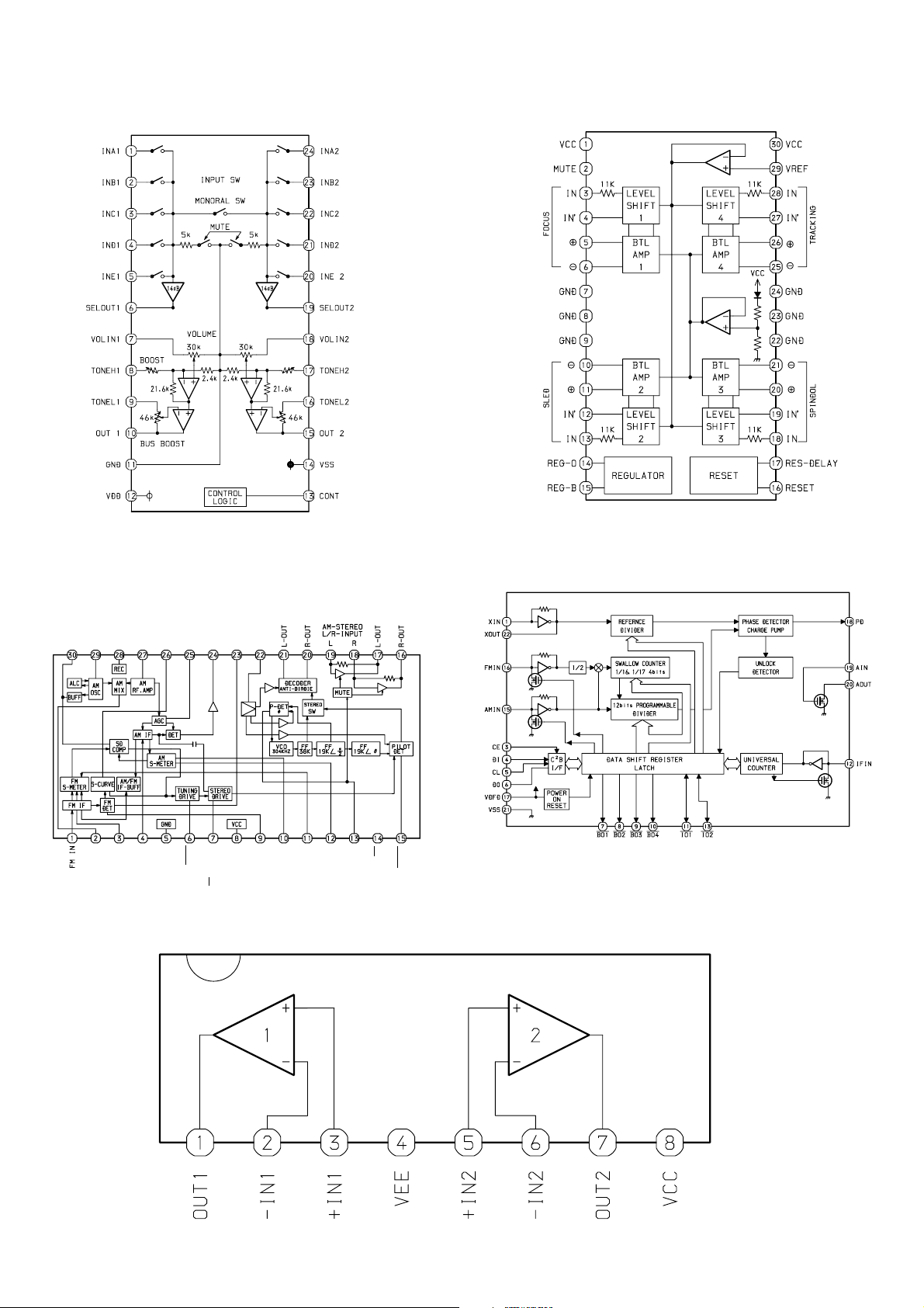
WIRING-1 (MAIN: HR)
101112131415161718192021222324
1234567892526272829303132
A
B
C
D
E
F
G
H
SH701
PLATE
I
J
K
L
M
N
O
P
Q
-9-
R
S
T
U
Page 10
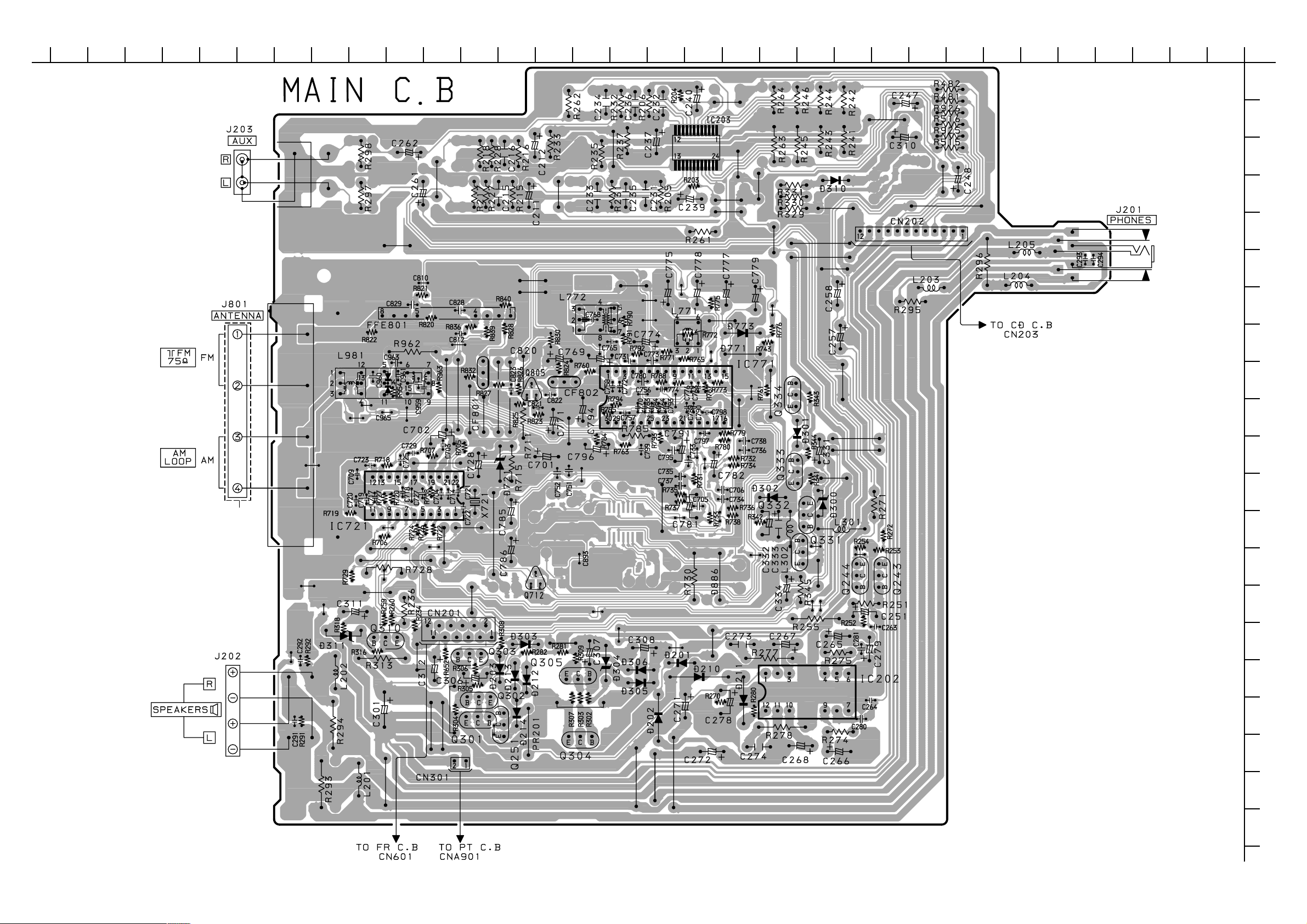
WIRING-2 (MAIN: K, EZ, HS)
C295, C296
EXCEPT HSSC
101112131415161718192021222324
1234567892526272829303132
A
B
C
D
E
F
SH701
PLATE
EXCEPT
K. EZ
K, EZ
EXCEPT HSSC
G
H
I
J
K
L
M
N
O
P
K, EZ
C298
EXCEPT
HSSC
Q
R
S
T
U
-10-
Page 11
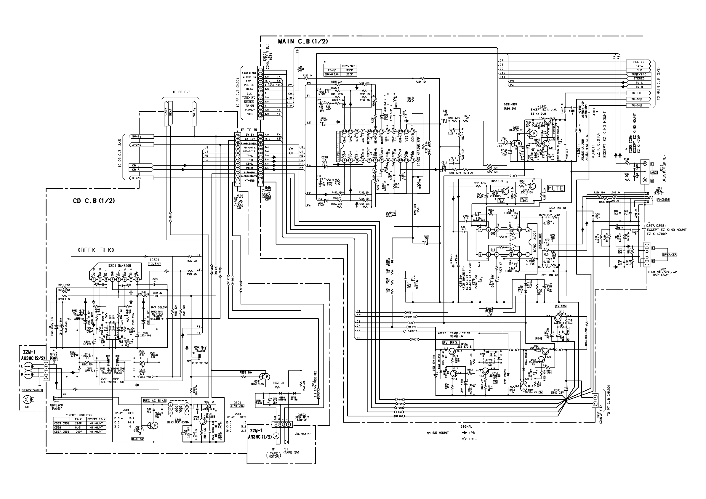
SCHEMATIC DIAGRAM-1 (MAIN)
(R/P SEL SW)
(R/P SEL SW)
-11-
Page 12

WIRING-3 (MOTOR)
123456789101112131415
A
B
C
D
E
MOTOR C.B
F
M2
G
CNA402
TO CD C.B
+
_
6
SW1
PIN3
1
M2
(SLED MOTOR)
SW1
(INSIDE LIMIT SW)
M3
M3
(SPINDLE MOTOR)
_
+
H
I
J
K
L
M
N
O
P
-12-
Q
R
S
T
U
Page 13

FL (AIWA4239ACL-13) GRID ASSIGNMENT/ANODE CONNECTION
GRID ASSIGNMENT
ANODE CONNECTION
-13-
Page 14

SCHEMATIC DIAGRAM-2 (TUNER: HR)
-14-
Page 15

SCHEMATIC DIAGRAM-3 (TUNER: K, EZ)
K, EZ
-15-
Page 16

WIRING-4 (FR, CD, LED)
101112131415161718192021222324
1234567892526272829303132
A
B
C
D
E
F
G
H
I
J
K
L
M
N
O
P
Q
PIN3
DECK MOTOR
R
RPH
S
EH
T
U
-16-
Page 17

SCHEMATIC DIAGRAM-4 (FRONT)
-17-
Page 18

SCHEMATIC DIAGRAM-5 (CD)
-18-
Page 19

WIRING-5 (PT)
EXCEPT K, EZ, HS
EZ, K, HS
HR, HT, HC, LH
K, EZ
EXCEPT K, EZ
K, EZ
HS
K, EZ
(HT, HC: JW)
HR, HT, HC, LH: AC 110-120V/220-240V 50/60Hz
K, EZ: AC 230V 50Hz
HS: AC 220V 60Hz
123456789101112131415
A
B
C
D
E
F
G
H
I
J
K
L
M
N
O
P
Q
-19-
R
S
T
U
Page 20

SCHEMATIC DIAGRAM-6 (POWER)
-20-
Page 21

ELECTRICAL ADJUSTMENT
<HR>
MAIN C.B (Component side)
J201
PHONES
!@
FR C.B
L771
0
68
L772
4
FFE801
6
IC771
15
30
28261716
L981
18
4
0
CD C.B (Component side)
M1 (TAPE MOTOR)
!
L501
@
IC401
20
SFR430
#
RPH
58
$
CN401
$
$
-
+
-21-
Page 22

<K, EZ, HS>
!@
J201
PHONES
MAIN C.B (Component side)
L771
0
L772
6
235
4
FFE801
9
FR C.B
2
TC942
L942
IC771
69
28261716
0
30
4
CD C.B (Component side)
58
IC401
20
9
L941
L981
7
M1 (TAPE MOTOR)
!
-22-
@
RPH
L501
#
SFR430
$
CN401
$
$
-
+
Page 23

< TUNER SECTION >
1. AM/MW VT Adjustment <HR>
Test point: FFE801 (4PIN)
Adjustment location: L981 (3/3)
7.5V±0.05V.......................................................... 1710kHz
0.3V (CHECK)....................................................... 530kHz
2. LW VT Adjustment <K, EZ, HS>
Test point: FFE801 (4PIN)
Adjustment location: L942
1.3V±0.05V............................................................ 144kHz
8.0V (CHECK)....................................................... 290kHz
3. MW VT Check <K, EZ, HS>
Test point: FFE801 (4PIN)
8.0V ........................................................................ 1602kHz
0.6V .......................................................................... 531kHz
< TAPE SECTION >
11. Tape speed Adjustment
Settings: • Test tape: TTA-100
• Test point: J201 (PHONES jack)
• Adjustment location: SFR of deck motor
Method: Play back the test tape and adjust SFR so that the
frequency counter reads 3000Hz ±30Hz.
12. Head Azimuth Adjustment
Settings: • Test tape: TTA-320
• Test point: J201 (PHONES jack)
• Adjustment location: Azimuth adjustment screw.
Method: Play back the 8kHz signal of the test tape and adjust
screw so that the output becomes maximum.
13. Bias frequency Adjustment
L501 .......................................................... 85kHz ±0.5kHz
4. Clock Frequency Check
Settings: Test point: IC771 (LA1837NL) 30PIN
Method: Set to AM 1602kHz and check that the test point
becomes 2052kHz±45Hz.
5. FM VT Check
Test point: FFE801 (4PIN)
8.0V ....................................................................108.0MHz
0.5V ......................................................................87.5MHz
6. IF Adjustment
Settings: • Test point: IC771 (LA1837NL) 16, 17PIN
• Adjustment location: L772
Method: Adjust L772 so that the output level at 1000kHz/
999kHz becomes maximum.
7. AM/MW Tracking Adjustment <K, EZ, HS>
L981 (1/3)............................................................... 603kHz
8. AM Tracking Adjustment<HR>
Settings: • Test point: IC771 (LA1837NL) 16, 17PIN
• Adjustment location: L981 (1/3)
Method: Adjust L981 (1/3) so that the output level at 1000kHz/
999kHz becomes maximum.
9. LW Tracking Adjustment <K, EZ, HS>
Settings: • Test point: IC771 (LA1837NL) 16, 17PIN
• Adjustment location: L941, TC942
Method: Set the TC942 to mechanical center.
Adjust L941 so that the output level at 144kHz
becomes maximum.
Adjust TC942 so that the output level at 290kHz
becomes maximum.
Repeat above procedure 2 or 3 times.
< CD SECTION >
14. FE Balance Adjustment
Settings: • Test point: -IC401, PIN58 (VR),
+IC401, PIN20 (FE)
• Adjustment location: SFR430
Method: Play back the disc and adjust SFR430 so that the test
point voltage becomes 0V.
10. DC Balance Adjustment
Settings: • Test point: IC771 (LA1837NL) 26, 28PIN
• Adjustment location: L771
• Frequency: 98.0MHz
Method: Set to FM 98.0MHz and adjust L771 so that the voltage
between 26PIN and 28PIN becomes 0V±0.04V.
-23-
Page 24

IC DESCRIPTION
IC, LA9241ML
Pin No. Pin Name I/O Description
1
FIN2
Pin to which external pickup photo diode is connected. RF signal is created by adding with the
I
FIN1 pin signal. FE signal is created by subtracting from the FIN1 pin signal.
10
11
12
13
14
15
16
2
3
4
5
6
7
8
9
FIN1
E
F
TB
TE-
TE
TESI
SCI
TH
TA
TD-
TD
JP
TO
FD
I
Pin to which external pickup photo diode is connected.
Pin to which external pickup photo diode is connected. TE signal is created by subtracting from
I
the F pin signal.
I
Pin to which external pickup photo diode is connected.
I
DC component of the TE signal is input.
I
Pin to which external resistor setting the TE signal gain is connected between the TE pin.
O
TE signal output pin.
TES “Track Error Sense” comparator input pin. TE signal is passed through a band-pass filter
I
then input.
I
Shock detection signal input pin.
I
Tracking gain time constant setting pin.
O
TA amplifier output pin.
Pin to which external tracking phase compensation constants are connected between the TD and
I
VR pins.
I
Tracking phase compensation setting pin.
I
Tracking jump signal (kick pulse) amplitude setting pin.
O
Tracking control signal output pin.
O
Focusing control signal output pin.
17
18
19
20
21
22
23
24
25
26
27
28
29
30, 31
FD-
FA
FA-
FE
FE-
AGND
SP
SPI
SPG
SP-
SPD
SLEQ
SLD
SL-, SL+
—
Pin to which external focusing phase compensation constants are connected between the FD and
I
FA pins.
Pin to which external focusing phase compensation constants are connected between the FD–
I
and FA– pins.
Pin to which external focusing phase compensation constants are connected between the FA and
I
FE pins.
O
FE signal output pin.
I
Pin to which external FE signal gain setting resistor is connected between the FE pin.
Analog signal GND.
O
Signal ended output of the CV+and CV- pin input signal.
I
Spndle amp input.
I
Pin to which external spindle gain setting resistor in 12 cm mode is connected.
Pin to which external spindle phase compensation constants are connected together with SPD
I
pin.
O
Spindle control signal output pin.
I
Pin to which external sled phase compensation constants are connected.
O
Sled control signal output pin.
I
Sled advance signal input pin from microprocessor.
32, 33
34
35
JP-, JP+
TGL
TOFF
I
Tracking jump signal input pin from DSP.
I
Tracking gain control signal input from DSP. Low gain when TGL = H.
I
Tracking off control signal input pin from DSP. Off when TOFF = H.
-24-
Page 25

Pin No. Pin Name I/O Description
36
TES
O
Pin from which TES signal is output to DSP.
37
38
39, 40
41
42
43
44
45
46
47
48
49
50
51
52
53
HFL
SLOF
CV–, CV+
RFSM
RFS-
SLC
SLI
DGND
FSC
TBC
NC
DEF
CLK
CL
DAT
CE
O
O
O
—
O
—
O
“High Frequency Level” is used to judge whether the main beam position is on top of bit or on
top of mirror.
I
Sled servo off control input pin.
I
CLV error signal input pin from DSP.
RF output pin.
I
RF gain setting and EFM signal 3T compensation constant setting pin together with RFSM pin.
“Slice Level Control” is the output pin which controls the RF signal data slice level by DSP.
I
Input pin which control the data slice level by the DSP.
Digital system GND.
Output pin to which external focus search smoothing capacitor is connected.
I
“Tracking Balance Control” EF balance variable range setting pin.
No connection.
Disc defect detector output pin.
I
Reference clock input pin. 4.23 MHz of the DSP is input.
I
Microprocessor command clock input pin.
I
Microprocessor command data input pin.
I
Microprocessor command chip enable input pin.
54
55
56
57
58
59
60
61
62
63
64
DRF
FSS
VCC2
REFI
VR
LF2
PH1
BH1
LDD
LDS
VCC1
—
—
—
O
“Detect RF” RF level detector output.
I
“Focus Search Select” focus search mode (± search/+ search) select pin. (Not connected)
Servo system and digital system Vcc pin.
Pin to which external bypass capacitor for reference voltage is connected.
O
Reference voltage output pin.
I
Disc defect detector time constant setting pin.
I
Pin to which external capacitor for RF signal peak holding is connected.
I
Pin to which external capacitor for RF signal bottom holding is connected.
O
APC circuit output pin.
I
APC circuit input pin.
RF system Vcc pin.
-25-
Page 26

IC, LC78622ED
Pin No. Pin Name I/O Description
1
DEFI
I
Defect sense signal (DEF) input pin. (Connect to 0V when not used).
2
3
4
5
6
7
8
9
10
11
12, 13
14
15
16
17
18
TAI
PDO
VVSS
ISET
VVDD
FR
VSS
EFMO
EFMIN
T2
CLV+, CLK-
___
V/P
HFL
TES
TOFF
TGL
—
—
—
I
O
For PLL.
I
I
Digital system GND. Be sure to connect to 0V.
O
For slice level control.
I
I
Test signal input pin with built-in pull-down resistor. Be sure to connect to 0V.
O
Disc motor control output. Three level output is possible using command.
Rough servo or phase control automatic selection monitoring output pin. Rough servo at H.
O
Phase servo at L.
I
Track detect signal input pin. Schmidt input.
I
Tracking error signal input pin. Schmidt input.
O
Tracking OFF output pin.
O
Tracking gain selection output pin. Gain boost at L.
Test signal input pin with built-in pull-down resistor. Be sure to connect to 0V.
Phase comparator output pin to control external VCO.
GND pin for built-in VCO. Be sure to connect to 0V.
Pin to which external resistor adjusting the PD0 output current.
Power supply pin for built-in VCO.
Pin for VCO frequency range adjustment.
EFM signal output pin.
EFM signal input pin.
19, 20
21
22
23
24
25
26
27
28
29
30
31
32, 33
34
35
36
37
JP+, JP-
PCK
FSEQ
VDD
SL+
SL-
—
PUIN
RW
EMPH
C2F
DOUT
T3, T4
N.C.
MUTEL
LVDD
LCHO
—
—
—
—
O
Track jump control signal output pin. Three level output is possible using command.
O
EFM data PB clock monitoring pin 4.3218 MHz when phase is locked in. (Not Connected)
Sync signal detection output pin. H when the sync signal which is detected from EFM signal and
O
thesync signal which is internally generated agree. (Not Connected)
Digital system power supply pin.
O
Moves the sled to outer circumference.
O
Moves the sled to inner circumference.
Not connected.
I
CD pickup inner switch detection.
O
Read, wright signal. (Not Connected)
O
De-emphasis monitor output pin. De-emphasis disc is being played back at H. (Not Connected)
O
C2 flag output pin. (Not Connected)
O
DIGITAL OUT output pin. (EIAJ format). (Not Connected)
I
Test signal input pin with built-in pull-down resistor. Be sure to connect to 0V.
Not used. Set the pin to open.
O
L-channel 1-bit DAC.
O
L-channel mute output pin. (Not Connected)
L-channel power supply pin.
L-channel output pin.
38
LVSS
—
L-channel GND. Be sure to connect to 0V.
-26-
Page 27

Pin No. Pin Name I/O Description
39
RVSS
—
R-channel GND. Be sure to connect to 0V.
40
41
42
43
44
45
46
47
48
49
50
51
52
53
54
55
RCHO
RVDD
MUTER
XVDD
XOUT
XIN
XVSS
SBSY
EFLG
PW
SFSY
SBCK
FSX
WRQ
RWC
SQOUT
—
—
—
O
R-channel 1-bit DAC.
R-channel output pin.
R-channel power supply pin.
O
R-channel mute output pin. (Not Connected)
Crystal oscillator power supply pin.
O
Pin to which external 16.9344 MHz crystal oscillator is connected.
I
Crystal oscillator GND pin. Be sure to connect to 0V.
O
Subcode block sync signal output pin. (Not Connected)
O
C1, C2, single and dual correction monitoring pin. (Not Connected)
O
Subcode P, Q, R, S, T, U and W output pin. (Not Connected)
Subcode frame sync signal output pin. Falls down when subcode enters standby. (Not
O
Connected)
I
Subcode read clock input pin. Schmidt input. (Be sure to connected to 0V when not in use.)
Pin outputting the 7.35 kHz sync signal which is generated by dividing frequency of crystal
O
oscillator. (Not Connected)
O
Subcode Q output standby output pin.
I
Read/write control input pin. Schmidt input.
O
Subcode Q output pin.
56
57
58
59
60
61
62
63
64
COIN
___________
CQCK
RES
T11
16M
4.2M
T5
______
CS
T1
I
Command input pin from microprocessor.
I
Command input read clock or subcode read input clock from SQOUT pin
I
LC78622 reset input pin. Set this pin to L once when the main power is turned on.
O
Test signal output pin. Use this pin as open (normally L output).
O
16.9344 MHz output pin.
O
4.2336 MHz output pin.
I
Test signal input pin with built-in pull-down resistor. Be sure to connect to 0V.
Chip select signal input pin with built-in pull-down resistor. Be sure to connect to 0V while it is
I
not controlling.
I
Test signal input pin without built-in pull-down resistor. Be sure to connect to 0V.
-27-
Page 28

IC, LC867132V-5S27
Pin No. Pin Name I/O Description
1
O-RMC/CE
O
CD read/write control output and TU CE.
10
11
12
13
14
15
16
17
18
2
3
4
5
6
7
8
9
O-DATA
O-CLK
—
O-CLK SFT
I-HOLD
I-RST
XT1 (IN)
XT2 (OUT)
VSS1
CF1 (IN)
CF2 (OUT)
VDD1
I-FM ST
I-KEYO
I-CD SW
I-KEY1
I-MOTOR
—
—
—
O
Data output to M62495FP.
O
Output CLK to tuner PLL.
Not Connected.
O
Clock shift output of the microcomputer.
I
Hold status detection.
I
Microcomputer reset.
I
Connected to 32.768KHZ crystal oscillator.
O
GND.
I
Connected to 6MHZ Ceramic Filter.
O
Power supply for microcomputer (+5V).
I
FM STEREO status input.
I
KEY AD input.
I
CD DOOR SW status detection input.
I
KEY AD input.
I
DECK MECHA MOTOR status input.
19
20
21
22
23
24
25
26
27
28
29
30
31
32
33
34
35
P85
P86
I-TU DO
O-BASS LED
O-QS LED
—
O-INT
I-DRF
I-WRQ
I-REMO
S0-PA0
S1/PA1
S2/PA2
S3/PA3
S4/PA4
S5/PA5
S6/PA6
—
I
REC status input. (Not connected)
I
FM, AM status input. (Not connected)
I
Data input from tuner PLL.
O
BASS LED ON/OFF control output. (Not connected)
O
Q-Sound LED ON/OFF control output. (Not connected)
Not connected.
O
INT DIODE MATRIX detection output.
I
CD RF level detection input.
I
CD sub-code Q standby input.
I
Remote control input.
O
LCD segment output. (SW)
O
LCD segment output. (LW)
O
LCD segment output. (MW 10K)
O
LCD segment output. (FM WIDE)
O
LCD segment output. (OIRT)
O
LCD segment output. (SW2)
O
LCD segment output. (ZCH)
36
37-40
41
42
43-51
52-54
S7/PA7
S8~S11
VDD3
VSS3
S12~S13, S16-S22
S23-S25
—
—
O
LCD segment output. (AM ST)
O
LCD segment output.
Power supply for microcomputer (+5V).
GND.
O
LCD segment output.
O
LCD segment output. (Not connected)
-28-
Page 29

Pin No. Pin Name I/O Description
55
O-CD LED
O
LED ON/OFF control output for CD functions. (Not connected)
56
57
58
59
60
61
62
63
64-66
67
68
69
70
71
72
73
74
O-TU LED
O-TA LED
O-ROCK LED
O-POP LED
O-JAZZ LED
—
I-CD TEST
I-TU TEST
COM0-COM2
—
VSS2
VDD2
O-CD ON
O-TU ON
O-P.CONT
—
O-MUTE
—
—
—
—
—
O
LED ON/OFF control output for TU functions. (Not connected)
O
LED ON/OFF control output for TAPE functions. (Not Connected)
O
LED ON/OFF control output for ROCK. (Not connected)
O
LED ON/OFF control output for POP. (Not connected)
O
LED ON/OFF control output for JAZZ. (Not connected)
I
Not connected.
I
O
LCD common output.
Not connected.
GND.
Power supply for microcomputer (+5V).
O
CD PWR control output.
O
TU PWR control output.
O
Power supply control output.
Not connected.
O
Main mute output.
75
76
77
78
79
80
O-FM MONO
O-BEAT CONT
O-QSOUND
O-COIN
I-SQOUT
O-CQCK
O
FM mono/stereo output.
O
BEAT switch over output.
O
Q-Sound ON/OFF output.
O
CD command output.
I
CD sub-code Q input.
O
CLK for CD commands/sub-codes.
-29-
Page 30

MECHANICAL PARTS LIST 1/1
REF. NO PART NO. KANRI DESCRIPTION
NO.
1 8A-CLD-096-010 WINDOW,CASS-E<EZL>
1 8A-CLD-007-010 WINDOW,CASS<EXCEPT EZL>
2 8A-CLD-006-010 BOX,CASS
3 8A-CLD-008-010 WINDOW,LCD<EXCEPT EZL>
3 8A-CLD-097-010 WINDOW,LCD-E<EZL>
4 8A-CLD-213-010 SPR-T,CASS
5 8A-CLD-216-010 CUSHION,FOOT
6 8A-CLD-001-010 CABI,FR
7 8A-CLD-011-010 BTN,FUNCTION
8 8A-CGD-010-010 BTN,CD-V<EZL>
8 8A-CLD-012-010 BTN,CD<EXCEPT EZL>
9 8A-CLD-010-010 BTN,VOL
10 8A-CLD-009-010 RING,VOL<EXCEPT EZL>
10 8A-CGD-009-010 RING,VOL-V<EZL>
11 87-063-164-010 OIL-DMPR 80
12 8A-CLD-013-010 BTN,EQ
13 8A-CLD-014-010 KEY,CASS
14 8Z-CT6-214-010 RING,CHUCK
15 8Z-CT6-213-010 BASE,CHUCK
16 87-036-368-010 MAGNET
17 86-CT9-222-010 PLATE,MAGNET
18 86-CT9-217-010 HLDR,CHUCK A(S)
19 8A-CGD-005-010 BOX,CD-V<EZL>
19 8A-CLD-004-010 BOX,CD<EXCEPT EZL>
20 8A-CLD-005-010 WINDOW,CD<EXCEPT EZL>
20 8A-CLD-095-010 WINDOW,CD-E<EZL>
21 8A-CLD-201-010 HLDR,LCD
22 8A-CLD-621-010 FF-CABLE,12P FR-MAIN
23 8A-CLD-622-010 CONN ASSY,2P DOOR
24 8A-CLD-211-010 SPR-P,REC
REF. NO PART NO. KANRI DESCRIPTION
25 8A-CLD-210-010 PLATE,REC
26 8A-CLD-620-010 FF-CABLE,16P CD-RF
27 8A-CLD-003-011 CHAS,CD
28 87-063-165-010 OIL-DMPR 150
29 8A-CLD-212-010 SPR-T,CD
30 87-036-389-010 SW,PUSH LOCK
31 M8-ZZK-E90-070 DA11T3C
32 8A-CLD-032-010 CABI,REAR LH<HR>
32 8A-CLD-033-010 CABI,REAR EZ<EXCEPT HR>
33 8A-CLD-214-010 HLDR,PT
!
34 87-A80-092-010 AC CORD ASSY,E BLK SUN FAI<EXCEPT HSS>
!
34 87-A80-155-010 AC CORD ASSY,HS TS<HSS>
35 8Z-CT9-064-010 PANEL CD
36 8A-CLD-625-010 CONN ASSY,4P TA-ME
37 8A-CLD-626-010 CONN ASSY,4P RPH
!
38 8A-CLD-642-010 PT,H<HR,HSS>
A 8A-CDA-222-010 S-SCREW,CASS+2.6-4
B 87-067-566-010 TAPPING SCREW, VFTT+3-6
C 87-661-097-410 TAPPING SCREW, VFT1+3-12
D 87-B10-118-010 QT2+3-12 W/O NI
E 87-741-102-410 UT2+3-20
F 87-751-094-410 VT2+3-6 W10SL0T
G 87-B10-269-010 UT2+3-12 W/O CR
H 87-741-096-410 UT2+3-10
I 8A-CK4-223-010 S-SCREW,CD
J 87-661-095-410 VFT1+3-8
NO.
COLOR NAME TABLE
Basic color symbol Color Basic color symbol Color Basic color symbol Color
B Black C Cream D Orange
G Green H Gray L Blue
LT Transparent Blue N Gold P Pink
R Red S Silver ST Titan Silver
T Brown V Violet W White
WT Transparent White Y Yellow YT Transparent Yellow
LM Metallic Blue LL Light Blue GT Transparent Green
LD Dark Blue DT Transparent Orange GM Metallic Green
YM Metallic Yellow DM Metallic Orange PT Transparent Pink
LA Aqua Blue
-30-
Page 31

MECHANICAL EXPLODED VIEW 1/1
PWB
19
18
17
16
15
14
20
PWB
HT-SINK
a
PWB
E
22
21
SH, LCD
LCD
7
9
8
H
23
PWB
24
B
H
J
26
H
27
37
A
28
35
36
CUSHION,
CD A
29
a
30
K
G
D
10
25
12
ZZM-1
13
31
I
CUSHION, CD A
H
C
CUSHION, CD A
38
33
11
3
2
4
5
1
6
32
B
PWB
H
HLDR, AC-CORD
5
G
34
D
-31-
Page 32

TAPE MECHANISM EXPLODED VIEW 1/1
12
11
TERMINAL,LB1
A
10
9
4
3
2
1
8
14
7
55
42
6
5
13
53
B
19
17
16
21
20
22
27
24
23
15
18
28
26
25
C
54
29
31
30
48
50
51
52
49
47
46
45
44
43
41
36
40
37
32
39
33
34
1
35
38
-32-
Page 33

TAPE MECHANISM PARTS LIST 1/1
REF. NO PART NO. KANRI DESCRIPTION
NO.
1 8Z-ZM1-254-310 SPR-C,REEL R
2 8Z-ZM1-225-110 GEAR,REEL R
3 8Z-ZM1-253-210 SPR-C,AUTO SENSOR
4 8Z-ZM1-217-110 LEVER,AUTO SENSOR
5 8Z-ZM1-212-110 LEVER,T-UP
6 8Z-ZM1-245-310 SPR-T,AUTO
7 8Z-ZM1-236-010 CLR,SLIP FF/REW
8 8Z-ZM1-252-110 SPR-C,FF/REW
9 8Z-ZM1-230-010 GEAR,SLIP FF/REW A
10 8Z-ZM1-269-010 FELT,FF/REW 2
11 8Z-ZM1-238-110 GEAR,SLIP FF/REW B 2
12 8Z-ZM1-237-110 LEVER,FF/REW 2
13 8Z-ZM1-283-010 LEVER,PAUSE 2
14 8Z-ZM1-222-010 LEVER,E-LOCK M
15 8Z-ZM1-219-010 LEVER,E-OPEN
16 8Z-ZM1-244-110 SPR-T,T-UP
17 8Z-ZM1-247-310 SPR-T,PINCH
18 8Z-ZM1-261-110 ROLLER ASSY,PINCH
19 8Z-ZM1-221-210 LEVER,PINCH
20 8Z-ZM1-205-310 LEVER,PLAY
21 8Z-ZM1-248-210 SPR-T,BRG
22 87-A91-830-010 HEAD,RP-7442
23 84-ZM2-227-310 SPR-C,AZIMUTH
24 8Z-ZM1-216-110 LEVER,AUTO
25 8Z-ZM1-246-110 SPR-T,AUTO 2
26 8Z-ZM1-233-110 GEAR,IDL REW
27 8Z-ZM1-208-010 LEVER,STOP
28 8Z-ZM1-207-010 LEVER,FF
29 8Z-ZM1-206-010 LEVER,REW
30 8Z-ZM1-211-210 LEVER,REC 2
REF. NO PART NO. KANRI DESCRIPTION
NO.
31 87-A91-819-010 HEAD,EH 2NSS-2200
32 8Z-ZM1-215-010 LEVER,REC LOCK
33 87-A91-492-010 SW,LEAF MSW18560
34 8Z-ZM1-226-010 GEAR,REEL L
35 8Z-ZM1-241-210 SPR-T,PLAY
36 8Z-ZM1-220-110 LEVER,REC SENSOR
37 8Z-ZM1-249-210 SPR-T,FR
38 8Z-ZM1-242-310 SPR-T,FF/REW
39 8Z-ZM3-244-010 GEAR,CAM TD20
40 8Z-ZM1-232-010 GEAR,IDL FF/REW
41 82-ZM1-290-010 FLY-WHL ASSY,ZZM1
42 8Z-ZM1-275-010 W-L,1.47-4-0.25
43 8Z-ZM1-228-010 GEAR,SLIP T-UP B
44 8Z-ZM1-265-010 FELT,T-UP
45 8Z-ZM1-227-010 GEAR,SLIP T-UP A
46 8Z-ZM1-251-210 SPR-C,T-UP SLIP
47 8Z-ZM1-243-310 SPR-T,STOP/PAUSE
48 87-A91-825-010 MOT,M09Y/Z
49 8Z-ZM1-271-010 PULLEY,MOT ZZM-1
50 8Z-ZM1-264-010 BELT,MAIN S
51 8Z-ZM1-260-010 SPR-P,CASETTE
52 8Z-ZM1-201-610 CHAS ASSY,ZZM-1
53 8Z-ZM1-255-310 SPR-T,E-LOCK
54 8Z-ZM1-214-210 LEVER,LOCK
55 8Z-ZM1-257-110 SPR-C,F/R
A 84-ZM2-242-010 S-SCREW,AZ1-2-6.4
B 8Z-ZM1-270-110 V+2.6 ZZM-1
C 87-B10-301-010 W-L,1.63-3.2-0.5 SLIT
-33-
Page 34

CD MECHANISM EXPLODED VIEW 1/1
SF-P101NR
CHASSIS
SHAFT,SLIDE
B
B
1
2
A
A
3
SPINDLE
MOTOR(M3)
CD MECHANISM PARTS LIST 1/1
REF. NO PART NO. KANRI DESCRIPTION
NO.
1 S2-121-A28-400 COVER GEAR
2 S2-511-A21-000 GEAR MIDDLE
3 S2-511-A21-100 GEAR,DRIVE
A S1-PN2-03R-OSE SCR PAN PCS 2-3
B 87-261-073-410 SCR S-TPG FLT 2.6-6
ALL M8-ZZK-E90-070 DA11T3C
MOTOR C,B
-34-
Page 35

SPEAKER PARTS LIST 1/1
REF. NO PART NO. KANRI DESCRIPTION
1 8A-CLD-635-010 SPKR,10MM 7OHM 8W Y000411
2 8A-CLD-025-010 FRAME,NET ASSY<EXCEPT EZL>
2 8A-CGD-012-010 FRAME,NET-V ASSY<EZL>
3 8A-CLD-021-010 CABI,SPKR-FR
4 8A-CLD-026-010 PLATE,GATE
5 8A-CLD-216-010 CUSHION,FOOT
A 87-741-096-410 UT2+3-10
B 87-741-104-410 UT2+3-30 GLD
NO.
-35-
Page 36

2–11, IKENOHATA 1–CHOME, TAITO-KU, TOKYO 110-8710, JAPAN TEL:03 (3827) 3111
737004
Printed in Singapore
 Loading...