

Page 1
CX-JT9
CASSETTE DECK
Track format 4 tracks, 2 channels stereo
Frequency response 50 Hz – 8 kHz
Recording system AC bias
Heads Deck A: playback x 1
Deck B: recording/playback x 1,
erase x 1
SERVICE MANUAL
Ver 1.0 2003.05
CX-JT9 is the tuner, amplifier , cassette dec k and
CD player section in JAX-PK9.
Model Name Using Similar Mechanism NEW
CD
Section
Tape deck
Section
CD Mechanism Type CDM74F-K6BD71A
Base Unit Name BU-K6BD71A
Optical Block Name KSM-213DCP
Optical Pick-up Name KSS-213D
Model Name Using Similar Mechanism NEW
Tape Transport Mechanism Type CWM43RR23
E Model
TUNER
FM tuning range 87.5 MHz to 108 MHz
FM usable sensitivity (IHF) 13.2 dBf
FM antenna terminal 75 ohms (unbalanced)
AM tuning range 530 kHz to 1710 kHz (10 kHz step)
531 kHz to 1710 kHz (9 kHz step)
AM usable sensitivity 350 µV/m
AM antenna Loop antenna
AMPLIFIER
Power output Front:
Rated: 156 W + 156 W (6 ohms,
T.H.D. 1 %, 1 kHz)
Reference: 195 W + 195 W (6 ohms,
T.H.D. 10 %, 1 kHz)
Front and Surround:
320 W + 200 W (Front Speaker: 6
ohms, Surround Speaker: 8 ohms,
T.H.D. 10 %, 1 kHz/DIN AUDIO)
Total harmonic distortion 0.08 % (98 W, 1 kHz, 6 ohms, DIN
AUDIO)
Input MD (VIDEO): 1.5 V
MIC: 1 mV (600 ohms)
Outputs FRONT SPEAKER: 6 ohms or more
SURROUND SPEAKER: 8 ohms or
more
PHONES: 32 ohms or more
SPECIFICATIONS
COPYRIGHT
Check copyright laws relevant to recordings from discs, tuner
or tape for the country where the unit is to be used.
Licensed by BBE Sound, Inc. under USP4638258, 5510752
and 5736897.
CD PLAYER
Laser Semiconductor laser
(λ = 780 nm)
Emission duration:
continuous
D/A converter 1 bit dual
Signal-to-noise ratio 85 dB (1 kHz, 0 dB)
Harmonic distortion 0.05 % (1 kHz, 0 dB)
GENERAL
Power requirements 120 V/220 V/230 V-240 V AC
(Switchable), 50 Hz/60 Hz
Power consumption 255 W
Power consumption With ECO mode on: 0.25 W
in standby mode With ECO mode off: 28 W
Dimensions (W x H x D) 280 x 328 x 446 mm
Weight 11.2 kg
Specifications and external appearance are subject to change
without notice.
COMPACT DISC DECK RECEIVER
9-877-262-01 Sony Corporation
2003E05-1 Home Audio Company
C 2003.05 Published by Sony Engineering Corporation
Page 2
CX-JT9
Notes on chip component replacement
•Never reuse a disconnected chip component.
• Notice that the minus side of a tantalum capacitor may be damaged by heat.
Flexible Circuit Board Repairing
•Keep the temperature of the soldering iron around 270 ˚C during repairing.
• Do not touch the soldering iron on the same conductor of the
circuit board (within 3 times).
• Be careful not to apply force on the conductor when soldering
or unsoldering.
CAUTION
Use of controls or adjustments or performance of procedures
other than those specified herein may result in hazardous radiation exposure.
This appliance is classified
CLASS 1 LASER PRODUCT
LUOKAN 1 LASER LAITE
KLASS 1 LASER APPARAT
as a CLASS 1 LASER
product.
This label is located on the
rear exterior.
SAFETY-RELATED COMPONENT WARNING!!
COMPONENTS IDENTIFIED BY MARK 0 OR DOTTED
LINE WITH MARK 0 ON THE SCHEMATIC DIAGRAMS
AND IN THE PARTS LIST ARE CRITICAL TO SAFE
OPERATION. REPLACE THESE COMPONENTS WITH
SONY PARTS WHOSE PART NUMBERS APPEAR AS
SHOWN IN THIS MANUAL OR IN SUPPLEMENTS PUBLISHED BY SONY.
2
Page 3

TABLE OF CONTENTS
CX-JT9
1. SERVICING NOTES ................................................ 4
2. GENERAL
Location of Controls ....................................................... 7
3. DISASSEMBLY
3-1. Disassembly Flow ........................................................... 9
3-2. Case (SIDE-L/R)............................................................. 10
3-3. Case (Top) ....................................................................... 10
3-4. Tray Panel........................................................................ 11
3-5. CD Mechanism Deck (CDM74F-K6BD71A)................ 11
3-6. Front Panel Section ......................................................... 12
3-7. Mechanical Deck ............................................................. 12
3-8. Rear Cabinet Section ...................................................... 13
3-9. Main Board...................................................................... 13
3-10. Power Board.................................................................... 14
3-11. Transformer Board.......................................................... 14
3-12 Table Assy ....................................................................... 15
3-13. Motor (TB) Board ........................................................... 15
3-14. Motor (LD) Board........................................................... 16
3-15. Base Unit (BU-K6BD71A)............................................. 16
3-16. Motor Gear Assy (Sled) (M701), BD Board .................. 17
3-17. Optical Pick-up (KSS-213D).......................................... 17
4. TEST MODE.............................................................. 18
5. ELECTRICAL ADJUSTMENTS
CD Section ...................................................................... 21
6. DIAGRAMS
6-1. Block Diagram – CD Section – ..................................... 22
6-2. Block Diagram – TUNER/TAPE/PANEL Section –..... 23
6-3. Block Diagram – AMP/POWER SUPPLY Section – ... 24
6-4. Note for Printed Wiring Boards and
Schematic Diagrams ....................................................... 25
6-5. Printed W iring Board – BD Board – ............................. 26
6-6. Schematic Diagram – BD Board – ................................ 27
6-7. Printed W iring Boards – CHANGER Section –............ 28
6-8. Schematic Diagram – CHANGER Section –................ 29
6-9. Schematic Diagram
– MAIN Board (1/4) (Suffix-11) – ................................. 30
6-10. Schematic Diagram
– MAIN Board (2/4) (Suffix-11) – ................................. 31
6-11. Schematic Diagram
– MAIN Board (3/4) (Suffix-11) – ................................. 32
6-12. Schematic Diagram
– MAIN Board (4/4) (Suffix-11) – ................................. 33
6-13. Printed Wiring Board – MAIN Board (Suffix-11) –..... 34
6-14. Printed Wiring Board – MAIN Board (Suffix-13) –..... 35
6-15. Schematic Diagram
– MAIN Board (1/4) (Suffix-13) – ................................. 36
6-16. Schematic Diagram
– MAIN Board (2/4) (Suffix-13) – ................................. 37
6-17. Schematic Diagram
– MAIN Board (3/4) (Suffix-13) – ................................. 38
6-18. Schematic Diagram
– MAIN Board (4/4) (Suffix-13) – ................................. 39
6-19. Printed Wiring Board – Power Board – (E51 model) ... 40
6-20. Printed Wiring Board – Power Board – (MX model) ... 41
6-21. Schematic Diagram – Power Board (1/2) –................... 42
6-22. Schematic Diagram – Power Board (2/2) –................... 43
6-23. Printed Wiring Boards – CD BUTTON/
HEADPHONE/MICROPHONE Boards – ..................... 44
6-24. Schematic Diagram – CD BUTTON/
HEADPHONE/MICROPHONE Boards – ..................... 45
6-25. Printed Wiring Board – PANEL Board – ...................... 46
6-26. Schematic Diagram – PANEL Board – ......................... 47
6-27. Printed Wiring Board – TRANSFORMER Board –
(E51 model)..................................................................... 48
6-28. Printed Wiring Board – TRANSFORMER Board –
(MX model)..................................................................... 49
6-29. Schematic Diagram – TRANSFORMER Board –
(E51 model)..................................................................... 50
6-30. Schematic Diagram – TRANSFORMER Board –
(MX model)..................................................................... 51
6-31. IC Pin Function Description ........................................... 55
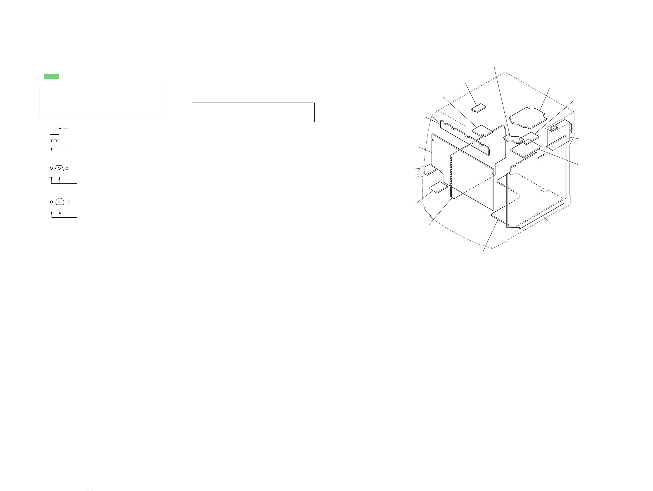
7. EXPLODED VIEWS
7-1. Case Section.................................................................... 61
7-2. Front Panel Section-1...................................................... 62
7-3. Front Panel Section-2...................................................... 63
7-4. Front Panel Section-3...................................................... 64
7-5. Front Panel Section-4...................................................... 65
7-6. Chassis Section-1 ............................................................ 66
7-7. Chassis Section-2 ............................................................ 67
7-8. CD Mechanism Deck Section-1
(CDM74F-K6BD71A) .................................................... 68
7-9. CD Mechanism Deck Section-2
(CDM74F-K6BD71A) .................................................... 69
7-10. CD Mechanism Deck Section-3
(CDM74F-K6BD71A) .................................................... 70
7-11. Base Unit Section (BU-K6BD71A) ............................... 71
8. ELECTRICAL PARTS LIST ............................... 72
•Abbreviation
E51 : Chilean and Peruvian models
MX : Mexican model
3
Page 4
CX-JT9
SECTION 1
SERVICING NOTES
NOTES ON HANDLING THE OPTICAL PICK-UP
BLOCK OR BASE UNIT
The laser diode in the optical pick-up block may suffer electrostatic break-down because of the potential difference generated
by the charged electrostatic load, etc. on clothing and the human
body.
During repair, pay attention to electrostatic break-down and also
use the procedure in the printed matter which is included in the
repair parts.
The flexible board is easily damaged and should be handled with
care.
NOTES ON LASER DIODE EMISSION CHECK
The laser beam on this model is concentrated so as to be focused
on the disc reflective surface by the objective lens in the optical
pick-up block. Therefore, when checking the laser diode emission, observe from more than 30 cm away from the objectiv e lens.
LASER DIODE AND FOCUS SEARCH OPERATION
CHECK
Carry out the “S curve check” in “CD section adjustment” and
check that the S curve waveforms is output three times.
UNLEADED SOLDER
Boards requiring use of unleaded solder are printed with the leadfree mark (LF) indicating the solder contains no lead.
(Caution: Some printed circuit boards may not come printed with
the lead free mark due to their particular size)
: LEAD FREE MARK
Unleaded solder has the following characteristics.
• Unleaded solder melts at a temperature about 40 ˚C higher than
ordinary solder.
Ordinary soldering irons can be used but the iron tip has to be
applied to the solder joint for a slightly longer time.
Soldering irons using a temperature regulator should be set to
about 350 ˚C.
Caution: The printed pattern (copper foil) may peel away if the
heated tip is applied for too long, so be careful!
• Strong viscosity
Unleaded solder is more viscou-s (sticky, less prone to flow)
than ordinary solder so use caution not to let solder bridges occur such as on IC pins, etc.
• Usable with ordinary solder
It is best to use only unleaded solder but unleaded solder may
also be added to ordinary solder.
• MODEL IDENTIFICATION
– Back Panel –
PART No.
MODEL PART No.
Chilean and Peruvian models 4-245-109-0
Mexican model 4-245-109-2
• DISCRIMINATION
Either type of the MAIN board, Part No. 1-688-080-11 or 1-688080-13 is used for Chilean and Peruvian models.
Note: For Mexican model, only one type of the MAIN board, Part No. 1-
688-080-13 is used.
How to identify the type is described below.
– MAIN BOARD (Conductor Side) –
D324
CN309
IC303
CN312
[]
[]
RELEASING THE DISC TRAY LOCK
The disc tray lock function for the antitheft of an demonstration
disc in the store is equipped.
Releasing Procedure :
While pressing the x key, press the Z key for 5 seconds. The
message “UNLOCKED” is displayed and the tray is unlocked.
Note: When “LOCKED” is displayed, the tray lock is not released by
turning power on/off with the [POWER] key.
4
D324
Suffix-11 ×
Suffix-13 a
Page 5
HOW TO OPEN THE DISC TRAY WHEN POWER SWITCH TURNS OFF.
1
Remove the case (side-L).
2
Turn the loading gear
in the direction of arrow A.
A
3
Pull-out the disc tray.
CX-JT9
5
Page 6
CX-JT9
SERVICE POSITION
– CD mechanism deck –
main board (CN312)
– Tape mechanism deck –
BD board (CN710)
panel board (CN601)
Connect wire (flat type) (19 core) to
main board (CN312) and BD board (CN710).
Connect wire (flat type) (13 core) to
panel board (CN601) and mechanical deck.
main board (CN203)
6
Page 7
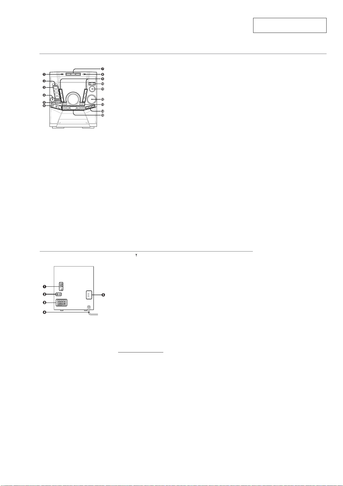
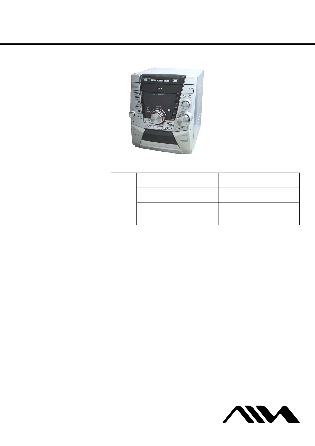
• LOCATION OF CONTROLS
# BASS
Adjusts low frequency sound.
SURROUND
Switches surround on and off.
i-Bass
Produces rich and clear low frequency sound.
$ DISPLAY
Displays the time and the remaining time for CD.
When the unit is off, press DISPLAY to switch between
DEMO, Clock and ECO display modes.
ALBUM k/i
Selects a previous album or a succeeding album with
MP3-CDs.
% rTUNING DOWN, t TUNING UP
(f , g)
CD: searches a track in fast forward or fast reverse
playback when held down.
Tape: fast forwards or rewinds the tape.
Tuner: manually tunes down or up within the band.
aPAUSE
CD and Tapes: pauses playback.
dDIRECTION
CD and Tapes: starts playback.
sSTOP
CD and Tapes: stops playback.
SECTION 2
GENERAL
CX-JT9
This section is extracted from
instruction manual.
Main unit: front
Refer to the pages indicated in parentheses for details.
1 DISC CHANGE/DISC SKIP
Rotates the CD trays.
2 POWER 6STANDBY/ON
Switches the unit on and off (standby).
The red indicator flashes when receiving a signal from
the remote.
3 TAPE A/B
Selects Tape function, and deck A or B.
TUNER BAND
Selects Tuner function and the radio band.
MD (VIDEO)
Selects the function of external equipment connected to
MD (VIDEO) jacks.
CD
Selects CD function.
4 TREBLE/MIDDLE
Enhances high or middle frequency sound.
5 CD SYNC
Starts Automatic CD dubbing.
REC PAUSE/START
Starts recording.
6 PHONES jack
Plug in here an optional headphones set with a mini
stereo plug (ø3.5 mm). Speaker output is canceled.
MIC jack
Connects the microphone here.
MIC MIXING
Adjusts the microphone volume.
7 DISC DIRECT PLAY 1-3
Selects a disc.
8 zOPEN/CLOSE
Opens or closes the disc compartment.
9 HEAVY, VOCAL, SALSA, TECHNO,
HIP HOP, MANUAL
Activates a graphic equalization curve.
0 MODE
Selects various modes (Play mode and Tape reverse, etc.)
when used in combination with ENTER and MULTI JOG.
ENTER
Fixes the modes and the time (Play mode and Tape
reverse, etc.) when used in combination with MODE and
MULTI JOG.
! MULTI JOG
CD: skips to a previous or a succeeding track.
Tuner: selects a preset station.
Clock and Timer: sets the time.
Selects the mode and the time when used in combination
with MODE and ENTER.
@ VOLUME
Adjusts the volume.
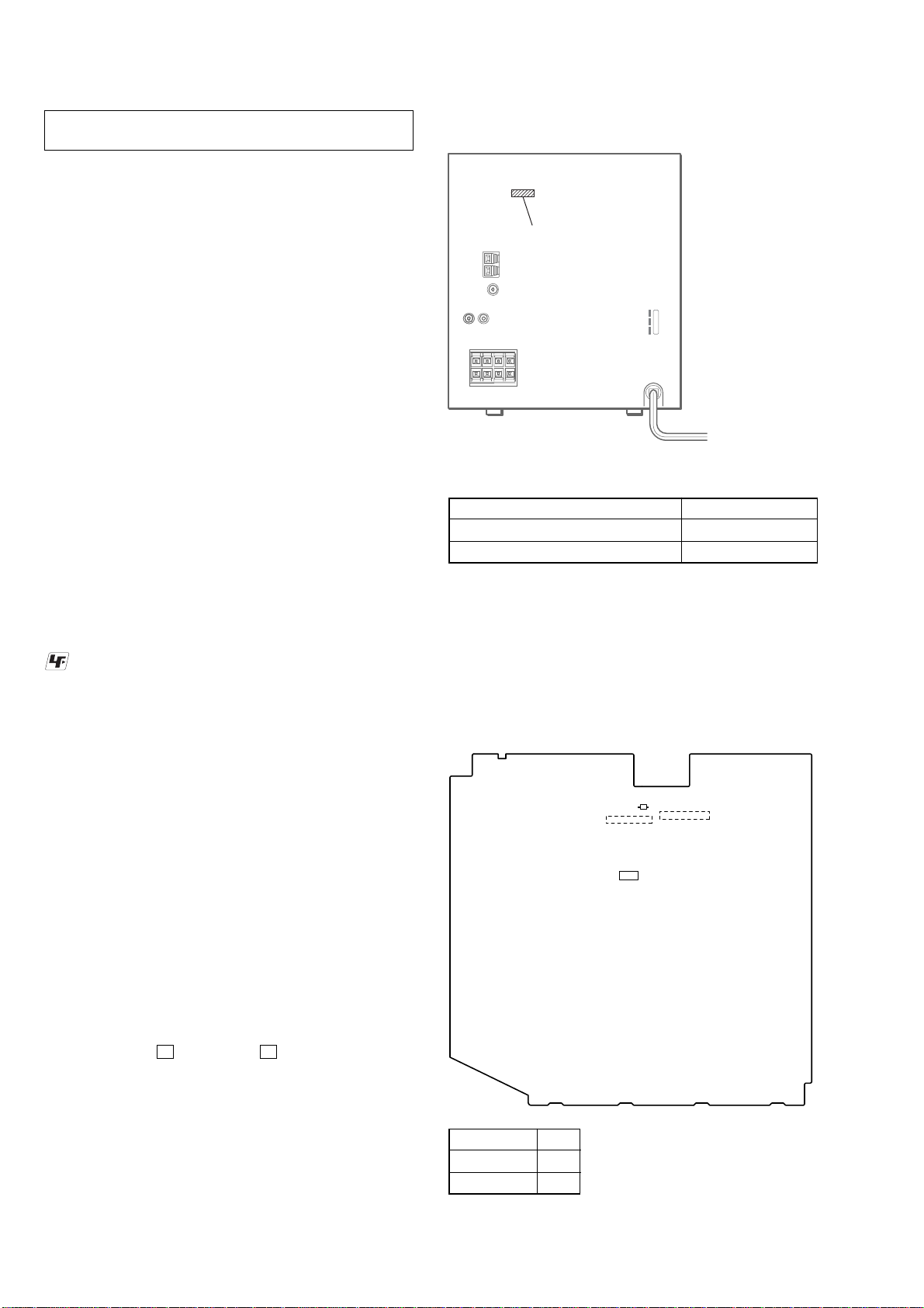
Main unit: rear
Refer to the pages indicated in parentheses for details.
1 AM LOOP, FM 75 Ω terminals
Plug in the supplied AM and FM antennas here.
2 MD (VIDEO) jacks
Accepts analog sound signals from external equipment.
Connect using an optional connecting cable with RCA
phono plugs (red plug to R jack, white plug to L jack).
Refer also to the operating instructions of your equipment.
To switch function to external input, press MD (VIDEO).
Tip:
To change the displayed name for this function, turn the
unit on, then hold down MD (VIDEO) and press POWER
on the unit. Repeat the procedure to select “MD” or
“VIDEO”.
3 SURROUND SPEAKER terminals
Connect for each speaker the blue cord to the 0 terminal
and the black cord to the 9 terminal.
FRONT SPEAKER terminals
Connect for each speaker the red cord to the 0 terminal
and the black cord to the 9 terminal.
4 AC power cord
5 AC VOLT AGE selector
Switches AC voltage among 120V, 220V, and 230V- 240V .
Make sure it matches your local voltage.
7
Page 8
CX-JT9
9 FUNCTION
Switches the active function among CD, TAPE, TUNER
and MD (VIDEO).
0 DISC SKIP
Select a disc.
! c/d
CD and Tape: starts playback.
s
CD and Tape: stops playback.
f, g
CD: searches a track in fast forward or fast reverse
playback when held down.
Tape: fast forwards or rewinds the tape.
Tuner: manually tunes down or up within the band.
a
CD and Tape: pauses playback.
@ SLEEP
Switches the sleep-timer on/off and selects the duration.
# VOLUME (+, -)
Adjusts the volume.
$ SOUND
Selects BASS, MID or TREBLE setting mode
CLEAR
Clears a track of the CD programed playback.
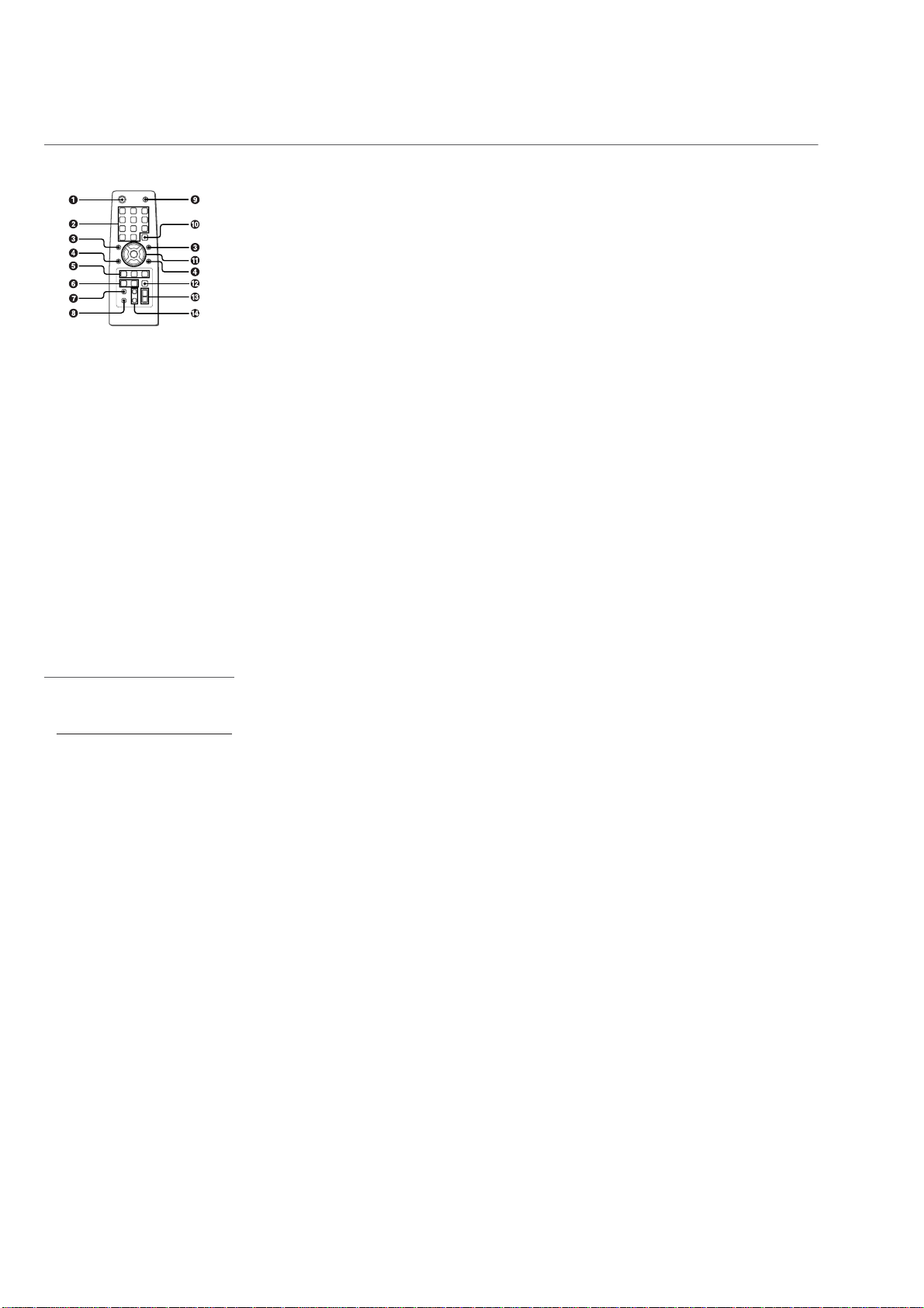
Remote control
Refer to the pages indicated in parentheses for details.
Buttons with the same or similar names with the main unit
basically have the same function.
1 POWER
2 1-0/10, +10
Selects a CD track of the specified number.
The numbered buttons take on these functions below when pressed
together with SHIFT held down
EDIT
Enters Automatic CD dubbing mode when pressed in
stop mode.
BAND
Selects Tuner function and the radio band.
TAPE A/B
Selects Tape function, and deck A or B.
SPECTRUM
Changes the spectrum analyzer display.
TUNER MODE
Switches between stereo or monaural FM reception.
KARAOKE
Selects Vocal Fader mode.
GEQ
Enters Graphic Equalizer setting mode.
TUNER MEMORY
Tuner: stores the received station in to preset.
SURROUND
Switches surround on and off.
:
3 r, t
CD: selects a track.
Tuner: selects a preset station.
BASS, MID and TREBLE: adjusts the level.
Clock and Timer: sets the time.
4 ALBUM M/N
Selects a previous album or a succeeding album.
5 PLAY MODE
CD: selects a playback mode.
Tape: selects a reverse mode
REPEAT
Enters CD repeat playback mode.
ENTER
6 CLOCK/TIMER/SET
Enters timer setting mode.
CLOCK/TIMER/SELECT (24, 25)
Selects timer playback, timer recording or timer off.
7 DISPLAY
Displays the time and the remaining time for CD.
When the unit is off, press DISPLAY to switch between
DEMO, Clock and ECO display modes.
8 SHIFT
Hold down when pressing a numbered button to change
its function to that printed above the number.
e.g.)
“Press SHIFT+BAND on the remote” indicates “Hold
down SHIFT and press ‘2’ (BAND)”. Doing so makes you
be able to select Tuner function and the radio band.
Setting the clock
Use the remote.
1
Press CLOCK/TIMER/SET .
Go to step 3 when the time appears and the ‘hour’ flashes.
2
Press r or t repeatedly until “CLOCK ”
appears in the display and then press ENTER.
3
Press r or t repeatedly to set the hour
and then press ENTER.
4
Press r or t repeatedly to set
and then press ENTER.
The time display stops flashing and the clock starts from
00 seconds.
•MULTI JOG is also available in place of r or t.
To di splay the time
Press DISPLAY . The time will be displayed for 6 seconds.
Tip:
“AM 12:00” indicates midnight and “ PM
If “- -:- -” appears when the unit is turned off
There has been a power interruption. Re-set the clock.
the
12:00
minute
” noon.
8
Page 9
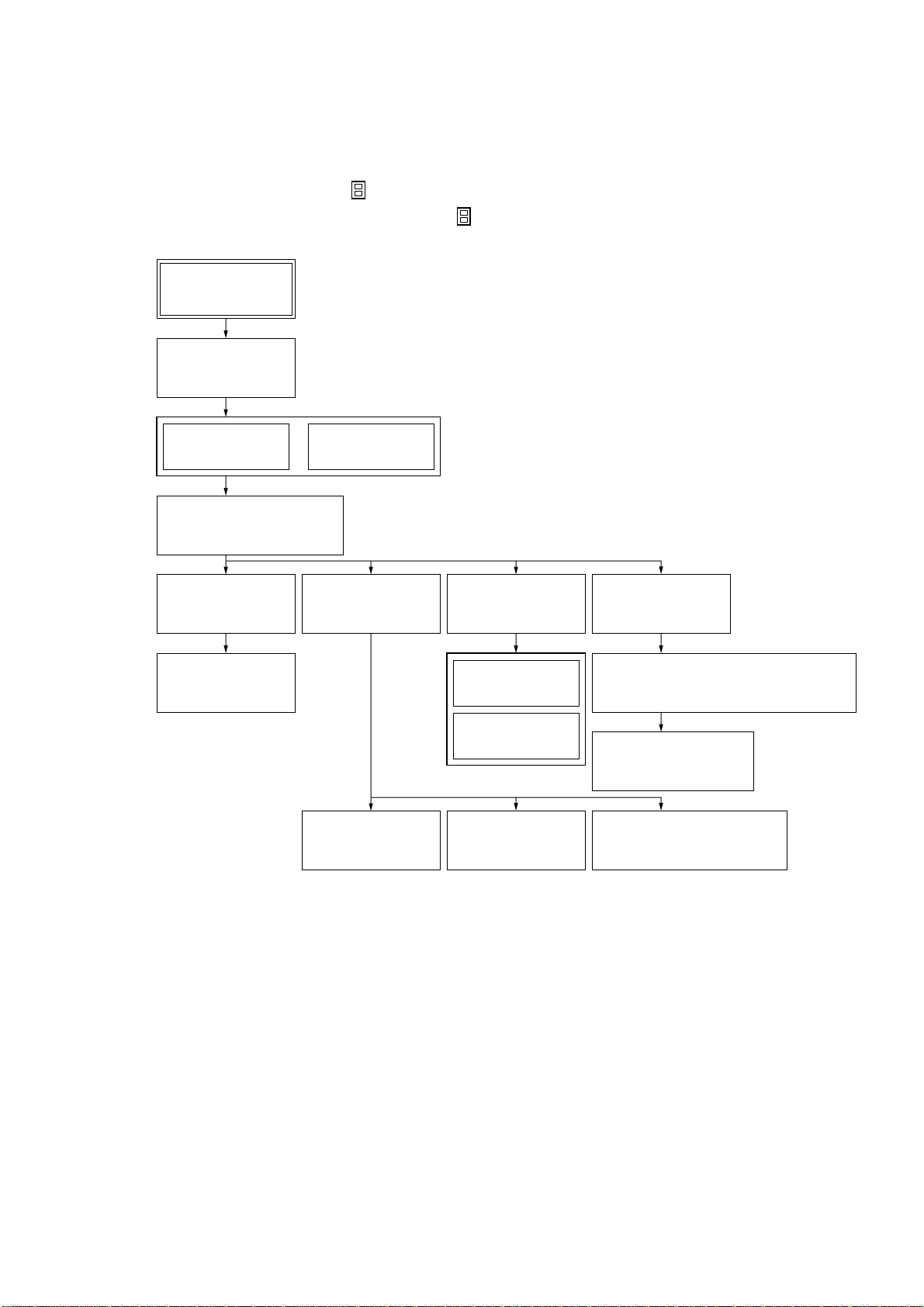
• This set can be disassembled in the order shown below.
3-1. DISASSEMBLY FLOW
Note 1: The process described in can be performed in any order.
Note 2: Without completing the process described in , the next process can not be performed.
Set
3-2. CASE
(SIDE-L/R)
(Page 10)
CX-JT9
SECTION 3
DISASSEMBLY
3-3. CASE (TOP)
(Page 10)
3-5. CD MECHANISM DECK
(CDM74F-K6BD71A)
(Page 11)
3-6. FRONT PANEL
SECTION
(Page 12)
3-7. MECHANICAL
DECK
(Page 12)
3-4. TRAY PANEL
3-8. REAR CABINET
3-9. MAIN BOARD
(Page 11)
SECTION
(Page 13)
(Page 13)
3-12. TABLE ASSY
(Page 15)
3-13. MOTOR (TB)
BOARD
(Page 15)
3-14. MOTOR (LD)
BOARD
(Page 16)
3-10. POWER
BOARD
(Page 14)
3-15. BASE UNIT
(BU-K6BD71A)
(Page 16)
3-16. MOTOR GEAR ASSY (SLED) (M701),
BD BOARD
(Page 17)
3-17. OPTICAL PICK-UP
(KSS-213D)
(Page 17)
3-11. TRANSFORMER BOARD
(Page 14)
9
Page 10
CX-JT9
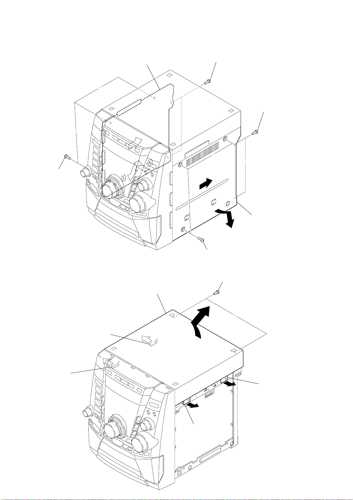
Note: Follow the disassembly procedure in the numerical order given.
3-2. CASE (SIDE-L/R)
7
three screws
(case3 TP2)
0
case (side-L)
8
9
6
3
two screws
(BVTP3 × 10)
4
1
two screws
(BVTP3 × 10)
5
case (side-R)
3-3. CASE (TOP)
4
claw
5
claw
7
case (top)
2
three screws
(case3 TP2)
6
1
two screws
(BVTP3 × 10)
2
claw
10
3
claw
Page 11
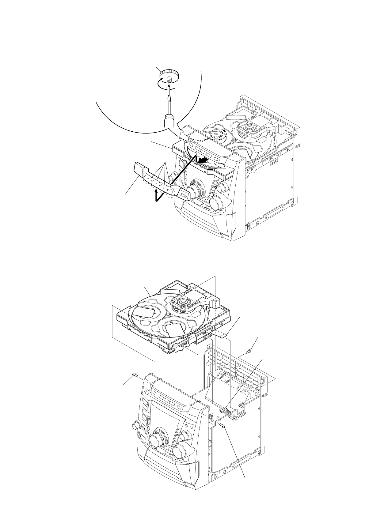
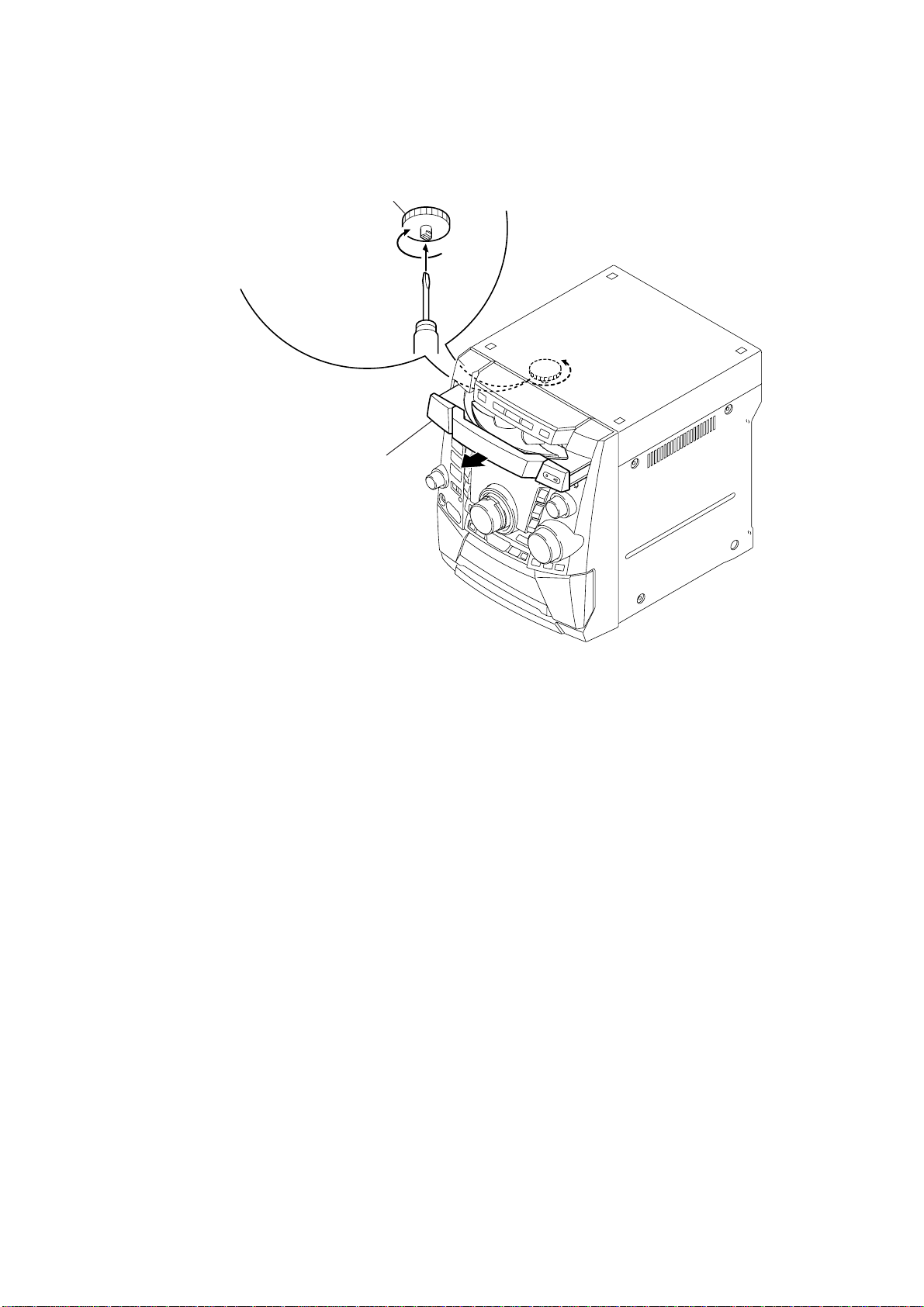
3-4. TRAY PANEL
1
Turn the loading gear
in the direction of arrow A.
2
Pull-out the disc table.
3
CX-JT9
A
four claws
tray panel
4
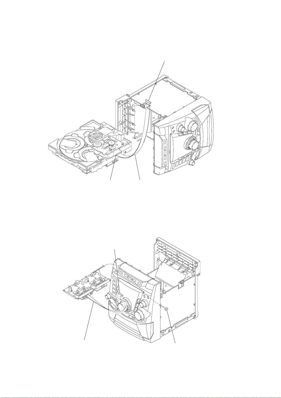
3-5. CD MECHANISM DECK (CDM74F-K6BD71A)
6
CD mechanism deck (CDM74F-K6BD71A)
1
wire (flat type) (19 core)
(CN312)
5
two screws
(BVTP3
2
connector (CN701)
×
10)
4
screw (BVTP3 × 10)
3
screw (BVTP3 × 10)
11
Page 12
CX-JT9
)
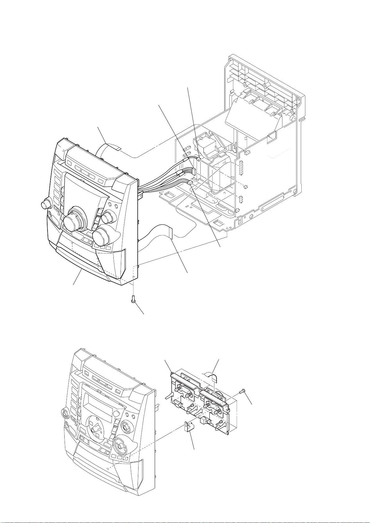
3-6. FRONT PANEL SECTION
5
wire (flat type) (9 core)
(CN311)
3
connector (CN202)
4
connector (CN203)
7
front panel section
3-7. MECHANICAL DECK
6
three screws
(BVTP3
3
mechanical deck
×
10)
2
1
wire (flat type) (31 core)
(CN304)
1
wire (flat type) (13core)
connector (CN310)
2
six screws
(BVTP3
×
10
12
4
ground mechanical plate
Page 13
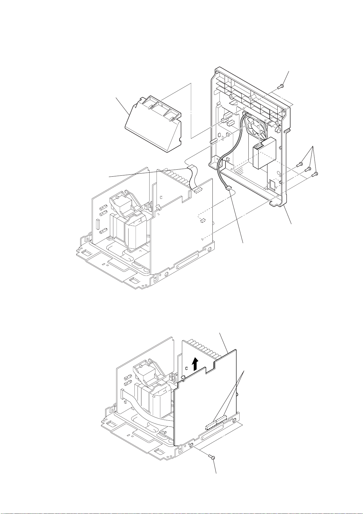
3-8. REAR CABINET SECTION
4
cover (duct)
1
wire (flat type) (11core)
3
two screws
(BVTP3
×
10)
5
five screws
(BVTP3
CX-JT9
×
10)
3-9. MAIN BOARD
3
main board
2
connector (CN303)
2
two connectors
(CN306, CN307)
6
rear cabinet section
1
two screws
(BVTP3
×
10)
13
Page 14
CX-JT9
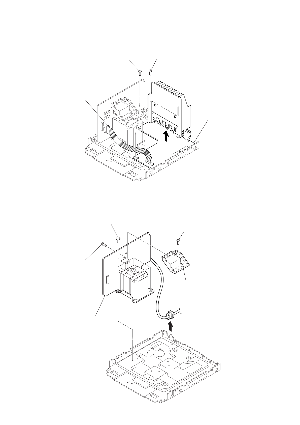
3-10. POWER BOARD
1
connector (CN902)
3
two screws
(BVIT3B+3-8R)
2
two screws
(BVIT3B+3-8R)
4
power board
3-11. TRANSFORMER BOARD
5
1
screw
(BVTP3
×
10)
6
transformer board
four screws
(ITC+4-10R)
4
2
screw
(BVTT3
3
trans holder
×
8)
14
Page 15
3-12. TABLE ASSY
)
d
two claws
5
CX-JT9
A
2
Pull-out the table assy.
6
table assy
3-13. MOTOR (TB) BOARD
1
screw
(PTPWH M2.6)
2
table (loading)
1
Turn the loading gear
in the direction of arrow
3
belt (table)
4
hook
3
wire (flat type) (5 core
(CN702)
A
.
4
connector
(CN731)
6
motor (TB) boar
5
two screws
(BTTP M2.6)
15
Page 16
CX-JT9
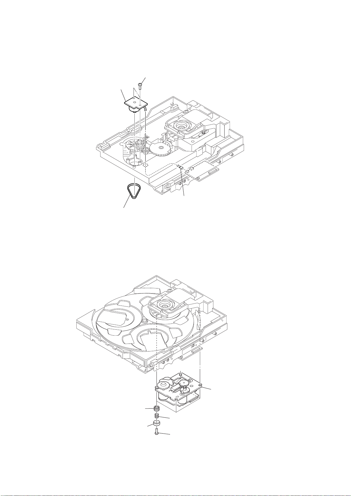
3-14. MOTOR (LD) BOARD
4
motor (LD) board
3
two screws
(BTTP M2.6)
1
3-15. BASE UNIT (BU-K6BD71A)
belt (loading)
2
connector
(CN704)
16
4
four insulators
2
four stoppers (BU)
3
four coil springs
(insulator)
1
four screws
(BTTP M2.6)
5
base unit (BU-K6BD71A)
Page 17
)
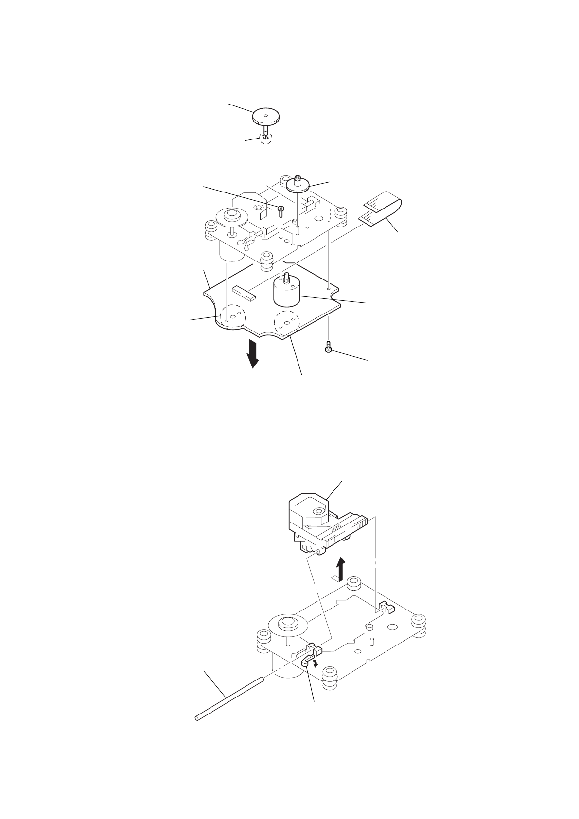
3-16. MOTOR GEAR ASSY (SLED) (M701), BD BOARD
7
gear (A)
6
claw
2
two screws
×
3)
(P2
qa
BD board
1
Remove two
solders.
8
gear (B)
5
wire (flat type) (16 core
(CN708)
0
motor gear assy (SLED)
(M701)
CX-JT9
3-17. OPTICAL PICK-UP (KSS-213D)
4
9
Remove two solders.
3
B
3
screw (P2.6 × 6)
Remove the optical pick-up
(KSS-213D) in the direction
of arrow
B
.
2
sled shaft
A
1
Slide the lever
in the direction of arrow
A
.
17
Page 18

CX-JT9
SECTION 4
TEST MODE
[COLD RESET]
• The cold reset clears all data including preset data stored in the
RAM to initial conditions. Execute this mode when returning
the set to the customer.
Procedure:
1. Press the [POWER] key to turn the power ON.
2. Press three keys of x , [ENTER] and [POWER] simultaneously.
3. The message “RESET” is displayed on the fluorescent indicator
tube momentarily, then becomes standby states.
[TUNER STEP CHANGE-OVER]
•A step of AM channels can be changed ov er between 9 kHz and
10 kHz.
Procedure:
1. Press the [POWER] key to turn the power ON.
2. Press the [TUNER BAND] key to select “AM”.
3. Press the [POWER] key to turn the power OFF.
4. Press two keys of [ENTER] and [POWER] simultaneously.
5. The message “9K STEP” or “10K STEP” is displayed on the
fluorescent indicator tube, and thus the channel step is changed
over.
[CD SHIP MODE]
• This mode moves the optical pick-up to the position durable to
vibration. Use this mode when returning the set to the customer
after repair.
Procedure:
1. Press the [POWER] key to turn the power ON.
2. Press the [CD] key to select “CD”.
3. Press two keys of [CD] and [POWER] simultaneously.
4. The message “LOCK” is displayed on the fluorescent indicator
tube, and the CD ship mode is set.
[CHANGE-OVER FUNCTION OF MD/VIDEO]
• This mode is used to enable function of external input to change
over between MD and VIDEO.
Procedure:
1. Set to standby state.
2. Press two keys of [MD VIDEO ]
3. The message “MD” or “VIDEO”is displayed on the
fluorescent indicator tube, and the function of external input
is changed over.
)(
and [POWER] simultaneously.
[CD TRAY LOCK MODE]
• This mode is used to unable to take sample disc out of tray in
the shop.
Procedure:
1. Press the [POWER] key to turn the power ON.
2. Press the [CD] key to select “CD”.
3. While pressing the x key, press the Z key for 5 seconds.
4. The message “LOCKED” is displayed on the fluorescent
indicator tube and the tray is locked. (Even if pressing
the Z key, the message “LOCKED” is displayed on the
fluorescent indicator tube and the tray is locked)
5. To release from this mode, while pressing the x key, press
the Z key for 5 seconds.
6. The message “UNLOCKED” is displayed on the fluorescent
indicator tube and the tray is unlocked.
[AMP TEST MODE]
• This mode is used to set the parameter of AMP IC and EQ band
level and i-bass IC.
Procedure:
1. Press the [POWER] key to turn the power ON.
2. P r ess three k eys of x , [HIP HOP] and [HEAVY] simultaneously.
3. When the AMP test mode is activated, the message “AMP
TEST” is displayed on the fluorescent indicator tube
momentarily.
4. Press two keys of [HEAVY] and [DISC DIRECT PLAY 2]
simultaneously, mode is changed over to parameter setting
of AMP IC and EQ band level and i-bass IC.
5. In the AMP IC setting mode, press the [ENTER] key, surround
ON/OFF is changed over.
6. In the EQ band level setting mode, press the [MANUAL] key,
EQ band is changed over to LOW, MID or HIGH.
7. In the i-bass IC setting mode, turn the
i-bass level, press the [i-BASS] key, i-bass f0 level is change
over between 1 to 3.
8. To release from this mode, press two keys of [HEAVY] and
[BASS] knob, up/down
[TECHNO] simultaneously.
18
Page 19
CX-JT9
[AGING MODE]
• This mode can be used for operation check of CD section and
tape deck section.
CD section and tape deck section work in parallel.
If an error occurred:
The aging operation stops only an error occurred sections and
display then status.
If no error occurs:
The aging operation continues repeatedly.
Procedure:
1. Press the [POWER] key to turn the power ON.
2. Press the [CD] key to select “CD”.
3. Set disc on the tray and set tape into the deck.
4. Set the “ALL DISCS” mode and “REV OFF” mode.
5. Press three keys of x , [HEAVY] and [DISC CHANGE/DISC SKIP]
simultaneously.
6. The message “AGING” is displayed on the fluorescent indicator
tube momentarily, then aging operations of CD and tape are
started at the same time.
7. To release from this mode, operate the “COLD RESET”.
1. Display at the Aging Mode
Display operating state of CD section and tape deck section
alternately.
If an error occurred, stop display which that section.
2. CD Section
The sequence during the aging mode is following as below.
Display at the aging mode is the same as the normal operation.
Aging mode sequence (CD section) :
3. Tape Deck Section
The sequence during the aging mode is following as below.
If an error occurred, stop display that step.
Aging mode sequence (tape deck section) :
Rewind the tape A and B
“AAG-1 or 2”
Shut off
FWD play the tape A
“AAG-3”
2 minutes
Fast forward the tape A
“AAG-4”
Shut off or 20 seconds
REV play the tape A
“AAG-5”
2 minutes
Rewind the tape A
“AAG-6”
Shut off
FWD play the tape B
“BAG-3”
Start (from disc 1)
Disc chucking
TOC read
Play first track for 2 seconds
Play last track for 2 seconds
EX-change open/close
Open the disc tray
Disc skip
Close the tray
Change the next disc.
2 minutes
Fast forward the tape B
“BAG-4”
Shut off or 20 seconds
REV play the tape B
“BAG-5”
2 minutes
Rewind the tape B
“BAG-6”
Shut off
Note: “*AG-*” is display of each step.
19
Page 20

CX-JT9
[GC TEST MODE]
• This mode is used to check the fluorescent indicator tube, LED
and key.
Procedure:
1. Press the [POWER] key to turn the power ON.
2. Press three keys of x , [HEAVY] and [DISC DIRECT PLAY 2]
simultaneously.
3. Fluorescent indicator tube and LEDs are all turned ON.
4. Press two keys of [HEAVY] and [DISC DIRECT PLAY 2]
simultaneously, mode is changed over.
5. In the key check mode, press each key, the def ined key number
of every each key list is displayed on the fluorescent indicator
tube.
6. In the key count check mode, “K-CNT 0” is displayed on the
fluorescent indicator tube. Each time a key is pressed, “K”
value increases. Howev er, once a ke y is pressed, it is no longer
taken into account.
7. In the headphone input check mode, connect the headphone,
the message “H_P ON” is displayed on the fluorescent indicator
tube, and disconnect the headphone, the message “H_P OFF”
is displayed on the fluorescent indicator tube.
8. In the volume check mode, turn the [VOLUME] knob, the
display on the fluorescent indicator tube is changed over to
“VOL UP”, “VOL FLAT” or “VOL DOWN”
[MC TEST MODE]
• This mode is used to check operations of Amplifier.
Procedure:
1. Press the [POWER] key to turn the power ON.
2. Press three keys of x , [HEAVY] and [DISC DIRECT PLAY 3]
simultaneously.
3. When the MC test mode is activated, the message “MC MODE”
is displayed on the fluorescent indicator tube momentarily, then
VACS level is displayed on the fluorescent indicator tube.
4. Press the
indicator tube is changed over to “EQ MAX”, press the
[TECHNO] key, the display on the fluorescent
[MANUAL] key, the display on the fluorescent indicator tube
is changed over to “EQ MID”, press the [HIP HOP] key,
the display on the fluorescent indicator tube is changed ov er
to “EQ MIN”,
5. Turn the [VOLUME] knob, the display on the fluorescent
indicator tube is changed over to “VOL MAX”, “VOL MID”
or “VOL MIN”
6. When the [REC PAUSE/START] key is pressed with a tape
set in the deck-B, the function is switched “MD” or “VIDEO”
and recording starts. When the m or M key is pressed
during recording, the tape is rewound back to the beginning of
recording, the function is switched to “T APE B”, then playback
starts.
7. When the [CD SYNC] key is pressed with the test tape (AMS-
100, AMS-110A) in the deck, number of space between tunes
is counted, then if AMS-110A is set, “OK” is displayed on the
fluorescent indicator tube and if AMS-100 is set, “NG” is
displayed on the fluorescent indicator tube.
8. To release from this mode, press the [POWER] key.
[MODEL, DESTINATION AND VERSION DISPLAY]
• This mode is used to check the model, destination and software
version.
Procedure:
1. Set to the standby state.
2. Pr ess three keys of x , [TECHNO] and [HEAVY] simultaneously.
3. When the model, destination and version display mode is
activated, the model an destination is displayed on the
fluorescent indicator tube.
4. Press two keys of [HEAVY] and [DISC DIRECT PLAY 2]
simultaneously, mode is changed ov er to model and destination
display mode and version display mode.
5. In the version display mode, press the [DISC DIRECT PLAY 3]
key, display is changed over to version display and year , month
and day of the software creation display.
6. To release from this mode, press the two keys of [TECHNO]
and [HEAVY] simultaneously.
[CD SERVICE MODE]
• This mode can run the CD sled motor freely. Use this mode, for
instance, when cleaning the optical pick-up.
Procedure:
1. Press the [POWER] key to turn the power ON.
2. Press the [CD] key to select “CD”.
3. Press three keys of x , [HEAVY] and Z simultaneously.
4. When the CD service mode is activated, the message “TRVS
ON” is displayed on the fluorescent indicator tube.
5. Press the M key, optical pick-up move to outside track and
the message “SLED OUT” is displayed on the fluorescent
indicator tube.
6. Press the m key, optical pick-up move to inside track and
the message “SLED IN” is displayed on the fluorescent
indicator tube..
7. Press the
[TECHNO] key, traverse ON/OFF is changed over.
[5 REPEAT LIMIT CANCEL]
• Number of repeat for CD playback is 5 times when the repeat
mode is “REPEAT”. This mode is used to enables CD to repeat
playback for limitless times.
Procedure:
1. Press the [POWER] key to turn the power ON.
2. Press the [CD] key to select “CD”.
3. Press three keys of x , [HEAVY] and Y simultaneously.
20
Page 21
p
p
SECTION 5
ELECTRICAL ADJUSTMENTS
CX-JT9
CD SECTION
Note:
1. CD Block is basically designed to operate without adjustment. Therefore,
check each item in order given.
2. Use YEDS-18 (3-702-101-01) unless otherwise indicated.
3. Use an oscilloscope with more than 10MΩ impedance.
4. Clean the object lens by an applicator with neutral detergent when the
signal level is low than specified value with the following checks.
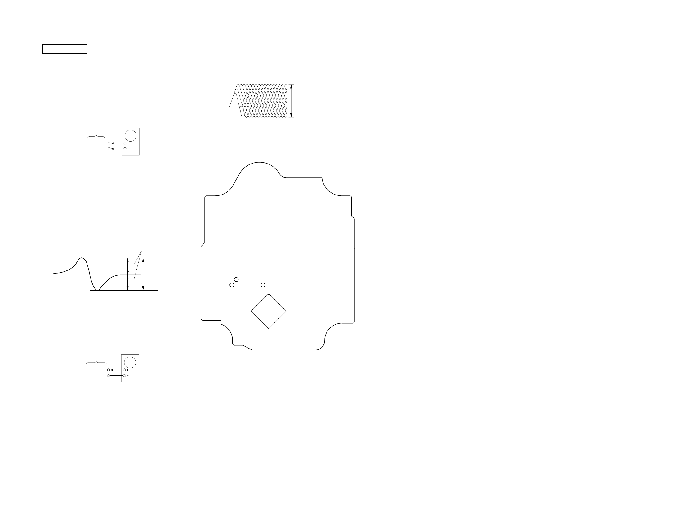
S-CURVE CHECK
Oscilloscope
BD board
TP(FE)
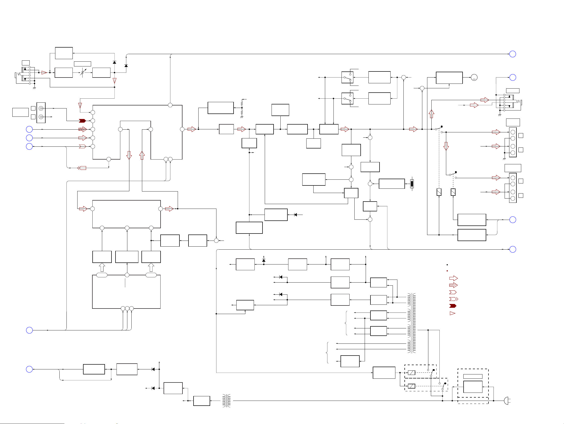
TP(VC)
Procedure :
1. Connect an oscilloscope to TP (FE) and TP (VC).
2. Turn the power on.
3. Load a disc (YEDS-18) and actuate the focus search. (In
consequence of open and close the disc tray, actuate the focus
search)
4. Confirm that the oscilloscope waveform (S-curve) is
symmetrical between A and B. And confirm peak to peak level
within 3 ± 0.5 Vp-p.
Note: Clear RF signal waveform means that the shape “ ◊ ” can be clearly
distinguished at the center of the waveform.
RF signal waveform
VOLT/DIV : 200mV
TIME/DIV : 500ns
±
level : 1.3
0.3Vp-
Connecting Location: BD board
– BD Board (Conductor side) –
S-curve waveform
symmetry
A
±
within 3
B
Note: •Try to measure several times to make sure than the ratio
of A : B or B : A is more than 10 : 7.
•Take sweep time as long as possible and light up the
brightness to obtain best waveform.
0.5Vp-
RF LEVEL CHECK
BD board
TP(RF)
TP(VC)
Procedure :
1. Connect an oscilloscope to TP (RF) and TP (VC).
2. Turn the power on.
3. Load a disc (YEDS-18) and playback.
4. Confirm that oscilloscope waveform is clear and check if RF
signal level is correct or not.
oscilloscope
TP (VC)
TP (RF)
TP (FE)
IC721
2121
Page 22
CX-JT9
SECTION 6
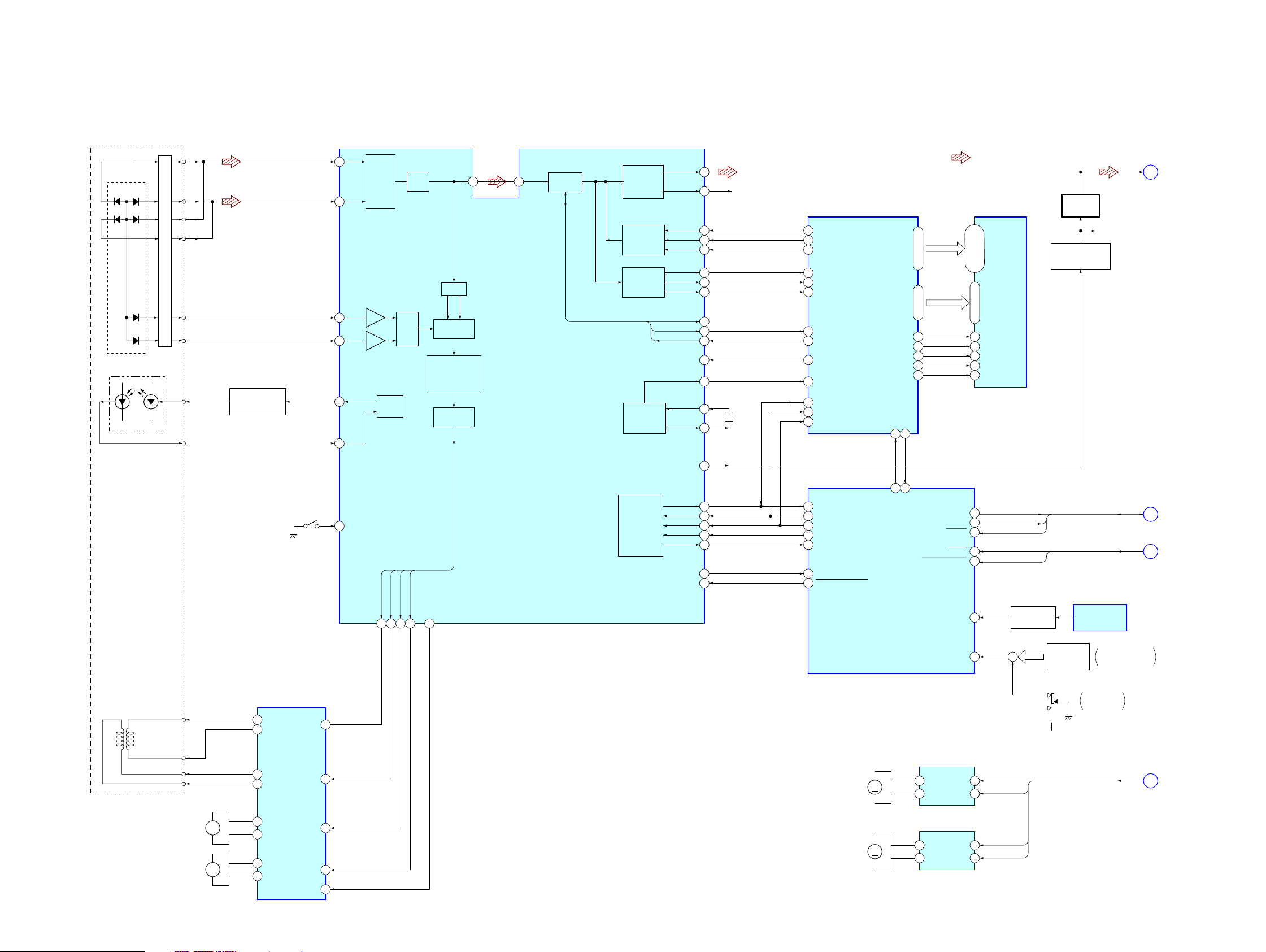
DIAGRAMS
6-1. BLOCK DIAGRAM – CD Section –
A
DETECTOR
A
D
C
B
E
F
LASER DIODE
PD
D
C
I-V AMP
B
E
F
LD
LD
PD
AUTOMATIC
POWER CONTROL
Q701
RF AMP, FOCUS/TRACKING ERROR AMP,
DIGITAL SIGNAL PROCESSOR, DIGIRAL SERVO PROCESSOR,
FIN2
8
RF
PH, BH
A/D
CONVERTER
SERVO
PROCESSOR
D/A
CONVERTER
4
APC
TBAL
EQ,
AGC
RF AMP
FIN1
7
TIN1
9
TIN2
10
LDD
80
LDS
79
3
EFMIN
DIGITAL FILTER, D/A CONVERTER
ERROR
CORRECT
IC721
D/A
CONVERTER
EXTERNAL
AUDIO IN
SERIAL OUT
CLOCK
GENERATOR
LCHO
RCHO
ASDFIN
ASDACK
ASLRCK
DATA
DATACK
LRSY
EFLG
C2F
FSX/16MIN
16MOUT
XIN
XOUT
42
45
57
56
55
60
59
58
53
52
50
26MP3RES
54
49
48
16.9344MHz
X701
R-CH
2 ADDATA
3 ADBCK
4 ADLRCK
79 DATAIN
80 DATACK
1 LRSY
5 C2FIN
9 CKOUT
78 RESB
7 CKIN
73 CMDOUT
74 CMDIN
75 CL
MP3 DECODER
IC801
CE
76 66
MDATA0
– MDATA15
MADRS0
– MADRS8
FSYNC
• R-ch is omitted due to same as L-ch.
• SIGNAL PATH
: CD PLAY
IC802
MEMORY
2-5, 7-10,
I/01 – I/016
23-30, 33-4060-53, 50
31-34, 36-39
A0 – A8
16-19, 22-26
27 OE45OEB
13 WE42WEB
14 RAS41RASB
29 LCAS43CASLB
28 UCAS44CASUB
MUTING
Q311
R-CH
MUTING CONTROL
SWITCH
Q312
CD-L
A
(Page 24)
OPTICAL PICK-UP
BLOCK
(KSM-213DCP)
2-AXIS
DEVICE
(FOCUS)
(TRACKING)
S701
(LIMIT)
FOCUS/TRACKING COIL DRIVE,
SPINDLE/SLED MOTOR DRIVE
IC722
VO3(+)
18
17 VO3(–)
11 VO2(+)
12 VO2(–)
FOIN
20TIN
10
70 LIMIT SW
TDO
FDO23SLDO22SPDO25CONT4
20
21
COMMAND
INTERFACE
*WRQ
72CD MUTE
106
DO
64
DI
63
CL
62
CE
61
65
67DRF
66*RES
99 I-LC78646/LC78684 DI
98 O-LC78646/LC78684 DO
100 O-LC78646/LC78684 CLK
5O-LC78646 CE
85 I-WRQ
86 I-CD DRF
4O-LC78646 RESET
SYSTEM CONTROLLER
IC901 (1/2)
M751
(LOADING)
M
O-LC78684 CE
I-LC78684 SYNC
I-BU IP DOWN/
CD OPEN CLOSE
LOADING MOTOR DRIVE
IC701
4 OUT1
2 OUT2
1O-SYS-MUTE
94O-POWER RELAY
29I-HOLD
11RESET
27I-POWER DOWN
96I-CD NUMBER SENS
22
7FIN
9RIN
S-MUTE
O-POWER
HOLD
RESET
POWER DOWN
LEVEL SHIFT
Q731
+
LM-F
LM-R
OPEN
CLOSE
ROTARY
ENCODER
S711
TABLE ADDRESS
S-MUTE,
O-POWER, HOLD
POWER DOWN
SENSOR
IC731
DISC TRAY
ADDRESS DETECT
S751
OPEN/CLOSE
DETECT
LM-F, LM-R,
TM-F, TM-R
RESET,
B
C
D
(Page 24)
(Page 24)
(Page 23)
M701
(SLED)
M702
(SPINDLE)
M
M
26 VO4(+)
27 VO4(–)
2 VO1(+)
1 VO1(–)
25SLIN
M741
M
(TABLE)
3SPIN
7LDS
TABLE MOTOR DRIVE
IC712
4 OUT1
2 OUT2
TM-F
7FIN
TM-R
9RIN
2222
Page 23
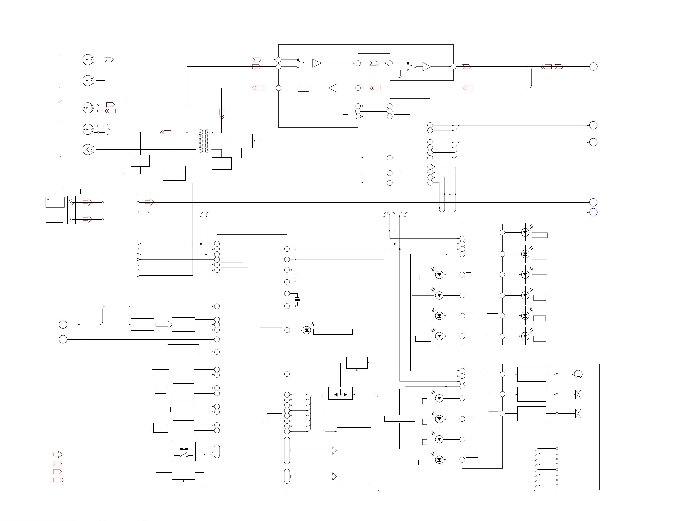
6-2. BLOCK DIAGRAM – TUNER/TAPE/PANEL Section –
L-CH
HP1
(PB)
(DECK-A)
HRPE1
(REC/PB/ERASE)
(DECK-B)
FM 75Ω
(COAXIAL)
AM LOOP
(Page 24)
(Page 24)
• R-ch is omitted due to same as L-ch.
• SIGNAL PATH
R-CH R-CH
L-CH
R-CH R-CH
ERASE
ANTENNA
MIC, SA
E
HP
F
: TUNER (FM/AM)
: TAPE PLAY (DECK-A)
: TAPE PLAY (DECK-B)
: REC
R-CH
TUNER UNIT
FM ANT
AM ANT
MIC
SA
MUTING
Q219, 221
L-CH
R-CH R-CH
DI
DO
CLK
CE
TUNED
ST
TU-MUTE
SPEANA AMP
Q201, 202
(FRONT PANEL KEY)
+3.3V (SUB)
VOLUME
BASS
MULTI JOG
TREBLE
MIDDLE
S301 – 309,
S311 – 331
REC ON/OFF
SWITCH
Q222, 225
BAND-PASS
FILTER
Q204 – 206
REMOTE CONTROL
RECEIVER
IC802
ROTARY
ENCODER
S801
ROTARY
ENCODER
S802
ROTARY
ENCODER
S803
ROTARY
ENCODER
S804
KEY ACTIVE
SWITCH
Q504, 505
BIAS OSC
L201
DI
CLK
+4V
REC BIAS
SWITCH
Q228
BIAS OSC
Q223
SYSTEM CONTROLLER
IC901 (2/2)
91 O-LC72121/M61529/BU2099 DO
87 I-LC72121 DI
92 O-LC72121/BU2099 CLK
9 O-LC72121 CE
88 I-TUNER TUNE
97 I-TUNER STEREO
21 I-MIC/I-TU SIG
18 I-SPEANA L
19 I-SPEANA M
20 I-SPEANA H
76 I-HP MUTE
28 I-RMC
84 I-VOL A
83 I-VOL B
80 I-BASS A
79 I-BASS B
82 I-JOG A
81 I-JOG B
78 I-TRE A
77 I-TRE B
I-KEY1 –
I-KEY3
26 – 24
+9V
O-BU2099 LCK
O-M61529 CLK
O-KEYSCAN
S7/I-A-PHOTO
S8/I-A-HALF
S6/I-A-MODE
S9/I-B-MODE
I-REC (FWD)
S10/I-REC (REW)
DECK A/B SELECT SWITCH, REC/PB EQ AMP
IC201 (SUFFIX-11) IC201 (SUFFIX-13)
AIN (L)
32
BIN (L)
34
RECOUT (L)
8
7
1312XT2
15
16
93O-POWER LED
95
48
52
49
53
47
54
50
55
S10/U11
41 – 45, 56 – 7131 – 40
S7/U5
S8/U6
S6/U4
S9/U10
EQ
X901
32.768kHz
X902
8.64MHz
U8
U9
U7
21
XT1
CF1
CF2
I-B-PHOTO
I-B-HALF
S1 – S5,
S11 – S26
G2 – G11
EQOUT (L)
REC-IN (L)
MUTE-ON/OFF
REC MUTE-ON/OFF
LED901
POWER 1 STANDBY/ON
B+
D603 – 610
S6 – S10
FLUORESCENT
INDICATOR TUBE
28 27
24
13
A/B
14
15
B+ SWITCH
Q921
FL901
MUTE
TAI (L)
MULTI CONTROLLER
IC309 (SUFFIX-11) IC309 (SUFFIX-13)
8
A/B
PB MUTE
9
10
REC MUTE
FRONT SPON/OFF
REAR SPON/OFF
LM-L (CD)
LM-R (CD)
TM-L (CD)
CLK
LCK
TM-R (CD)
S-OUT
LED201
CD
LED202
TUNER BAND
LED203
MD (VIDEO)
LED204
TAPE A/B
LED301
1
LED302
2
LED303
3
LED213
i-BASS
7 BIAS
6 REC
11 TUNER MUTE
DI
MCLK
+3.3V
DISC DIRECT PLAY
PB-OUT (L)
16
17
13
12
15
14
3DATA
4CLOCK
5LCK
18SO
CX-JT9
TAPE-L, REC-L
SP-F, SURR
LM-F, LM-R, TM-F, TM-R
TUNER-L
DI, SO, CLK, MCLK, LCK,
TAPE MECHANISM
DECK BLOCK
CAPM+
MM
(CAPSTAN/REEL)
A-SOL
(DECK-A)
B-SOL
(DECK-B)
A-PHOTO
B-PHOTO
A-HALF
B-HALF
A-MODE
B-MODE
REC (FWD)
REC (REW)
G
H
D
J
K
(Page 24)
(Page 24)
(Page 22)
(Page 24)
(Page 24)
15MANUAL
14HIP POP
13TECHNO
12SALSA
11VOCAL
10HEAVY
10
11
12
TAPE-L
REC-L
CAPSTAN/REEL
MOTOR DRIVE
Q601
PLUNGER DRIVE
(DECK-A)
Q602
PLUNGER DRIVE
(DECK-B)
Q603
LED211
MANUAL
LED210
HIP POP
LED208
TECHNO
LED207
SALSA
LED206
VOCAL
LED205
HEAVY
U5
U8
U6
U9
U4
U10
U7
U11
26
SP-F
SURR
LM-F
LM-R
TM-F
TM-R
SO
LCK
CLK
S-OUT
3 DATA
4 CLOCK
5 LCK
18 SO
6CD
7 TUNER
8 AUX
9 TAPE
LED DRIVER
IC201
3 DATA
4 CLOCK
5 LCK
18 SO
6 CD1
7 CD2
8 CD3
9 I-BASS
TAPE MECHANISM CONTROLLER
MOTOR
A-SOL
B-SOL
LED DRIVER,
IC202
2323
Page 24
CX-JT9
6-3. BLOCK DIAGRAM – AMP/POWER SUPPLY Section –
J401
MD (VIDEO)
IN
(Page 22)
(Page 23)
(Page 23)
(Page 23)
MIC
JK302
L
R
CD-L
A
TUNER-L
J
TAPE-L, REC-L TAPE-L
G
DI, SO, CLK,
MCLK, LCK
K
MIC LEVEL
MIC AMP
IC401 (1/2)
R-CH
AGC
Q401
REC-L
VR401
MIC MIXING
D401
MIC AMP
IC401 (2/2)
MIC
2
MD-L
37
CD-L
40
TUNER-L
39
TAPE-L
38
INA
1
FREQUENCY
CONTROL
Q314 – 316
12 – 10
CTRL1 –
CTRL3
14
D402
INPUT SELECTSWITCH, TONE CONTROL,
ELECTRICAL VOLUME, BASS BOOST AMP
IC301 (SUFFIX-11) IC301 (SUFFIX-13)
29
TOUT
RECB-2
35
BASS BOOST ENHANCER
IC303 (SUFFIX-11) IC303 (SUFFIX-13)
VREF
BASS BOOST
ON/OFF SWITCH
Q323
BASS BOOST CONTROLLER
IC310 (SUFFIX-11) IC310 (SUFFIX-13)
3
SO
MIC
BBE
7
9
I-BASS
DATA4CLOCK
5
LCK
CLK
LCK
VOLIN2
28
OUTA
GIN
13
BASS BOOST
CONTROL
Q317 – 320
16 – 13
BB CTRL1 –
BB CTRL4
SA
19
DATA22CLOCK
21
MCLK
DI
6
BASS BOOST
CONTROL
Q492
SAOUT
OUT2
MIC, SA
SWITCHING
Q18
R-CH
SWITCHING
Q17, 19, 22
VM+10V
CENTER VOLATAGE
GENERATOR
Q324
IC304 (SUFFIX-11) IC304 (SUFFIX-13)
25
FEED BACK
SWITCH
Q491
BUFFER
+
+1.8V
O-POWER
(MP3)
IC304
R-CH
VCC
MUTING CONTROL
+1.8V
REGULATOR
IC803
B+ SWITCH
Q301, 302
MUTING
Q525
SWITCH
Q527
S-MUTE
DECK+9V, M+9V
PRE DRIVE
Q517, 519
R-CH
+3.3V (MAIN)
CURRENT
MIRROR
Q521, 523
CASCADE
Q511, 513, 515
D102
D513
REGULATOR
IC306
POWER OFF
MUTING DRIVER
Q529, 530
IC306 (SUFFIX-11) IC306 (SUFFIX-13)
D313 – 315
P+7V
VM+9V
VM+10V
+4V
R-CH
–VP
+VP
FINAL DRIVE
Q501, 503
BIAS
Q507, 509
OVER CURRENT
DETECT
Q13
VM+10V
REGULATOR
IC305 (SUFFIX-11) IC305 (SUFFIX-13)
REGULATOR
IC308 (SUFFIX-11) IC308 (SUFFIX-13)
REGULATOR
IC313 (SUFFIX-11) IC313 (SUFFIX-13)
TO
POWER AMP
BLOCK
OVER LOAD
R-CH
+9V
IC305
+9V
IC308
+10V
IC313
DETECT
Q505
+
+
HOLD
Q12
+VH
–VH
+VL
–VL
R-CH
+VH
+VL
–VH
–VL
DC DETECT
RELAY B++9V
OUTPUT LEVEL
DETECT
Q20, 21
OUTPUT LEVEL
DETECT
Q23, 24
+
Q5, 6
+
HOLD
Q7 – 9
+
HOLD
RECT
D301 – 304
RECT
D319 – 322
RECT
RECT
THERMAL DETECT
Q10, 11
O-POWER
D1
D2
+
R-CH
MAIN POWER
TRANSFORMER
PT901
VM
VM
VH
VH
VL
VL
R-CH
TH501,
502
FAN MOTOR
ON/OFF SWITCH
Q327, 328, 372, 373
M731
M
(FAN)
+
R-CH
R-CH
RY501
RY502
R-ch is omitted due to same as L-ch.
SIGNAL PATH
R-CH
SURROUND SPEAKER
ON/OFF RELAY DRIVE
Q532
FRONT SPEAKER
ON/OFF RELAY DRIVE
Q304
S-MUTE, O-POWER, HOLD
: TUNER (FM/AM)
: CD PLAY
: TAPE PLAY
: REC
: MD (VIDEO) IN
: MIC INPUT
SURR
SP-F
SP-F,
SURR
E
HP
J221
PHONES
JK503 (1/2)
FRONT
SPEAKER
JK503 (2/2)
SURROUND
SPEAKER
H
B
F
+
–
+
–
+
–
+
–
(Page 23)
(Page 23)
L
R
L
R
(Page 23)
(Page 22)
(Page 22)
RESET,
POWER DOWN
C
RESET
POWER DOWN
RESET SWITCH
Q901
RESET SIGNAL
GENERATOR
IC502
+3.3V (SUB)
D504
+4V
+4V
REGULATOR
IC501
EVER+10V
RECT
D902 – 905
SUB POWER
TRANSFORMER
PT902
VF1
TO
FLUORESCENT
INDICATOR TUBE
VF2
–VFL
–30V
REGULATOR
Q533 – 536
POWER ON/OFF
RELAY DRIVE
Q330, 331
(Chilean, Peruvian)
RY901
RY902
(Mexican)
(Chilean, Peruvian)
S901
AC VOLTAGE
VOLTAGE
SELECTOR
(Mexican)
(AC IN)
2424
Page 25
CX-JT9
6-4. NOTE FOR PRINTED WIRING BOARDS AND SCHEMATIC DIAGRAMS
Note on Printed Wiring Board:
• X : parts extracted from the component side.
• Y : parts extracted from the conductor side.
• : Pattern from the side which enables seeing.
(The other layers' patterns are not indicated.)
Caution:
Pattern face side: Parts on the pattern face side seen from
(Conductor Side) the pattern face are indicated.
Parts face side: Parts on the parts face side seen from
(Component Side) the parts face are indicated.
• Indication of transistor.
C
Q
B
E
B
B
These are omitted.
Q
CE
These are omitted.
Q
CE
These are omitted.
Note on Schematic Diagram:
• All capacitors are in µF unless otherwise noted. pF: µµF
50 WV or less are not indicated except for electrolytics
and tantalums.
• All resistors are in Ω and 1/
specified.
• 2 : nonflammable resistor.
• C : panel designation.
Note: The components identified by mark 0 or dotted line
with mark 0 are critical for safety.
Replace only with part number specified.
• A : B+ Line.
• B : B– Line.
•Voltages and waveforms are dc with respect to ground
under no-signal (detuned) conditions.
no mark : FM
(): CD PLAY
[]: TAPE PLAY (DECK-A)
{ } : TAPE PLAY (DECK-B)
〈〈 〉〉 : REC
•Voltages are taken with a V OM (Input impedance 10 MΩ).
Voltage variations may be noted due to normal production tolerances.
•Waveforms are taken with a oscilloscope.
Voltage variations may be noted due to normal production tolerances.
• Circled numbers refer to waveforms.
• Signal path.
F : TUNER (FM/AM)
J : CD PLAY
E : TAPE PLAY (DECK-A)
d : TAPE PLAY (DECK-B)
G : REC
j : MD (VIDEO) IN
N : MIC INPUT
•Abbreviation
E51 : Chilean and Peluvian models
MX : Mexican model
: Impossible to measure
∗
4
W or less unless otherwise
• Circuit Boards Location
MOTOR (LD) board
CD BUTTON board
PANEL board
HEADPHONE board
MICROPHONE board
TRANSFORMER board
SENSOR board
SW board
BD board
MOTOR (TB) board
TUNER PACK
DRIVER board
MAIN board
POWER board
2525
Page 26
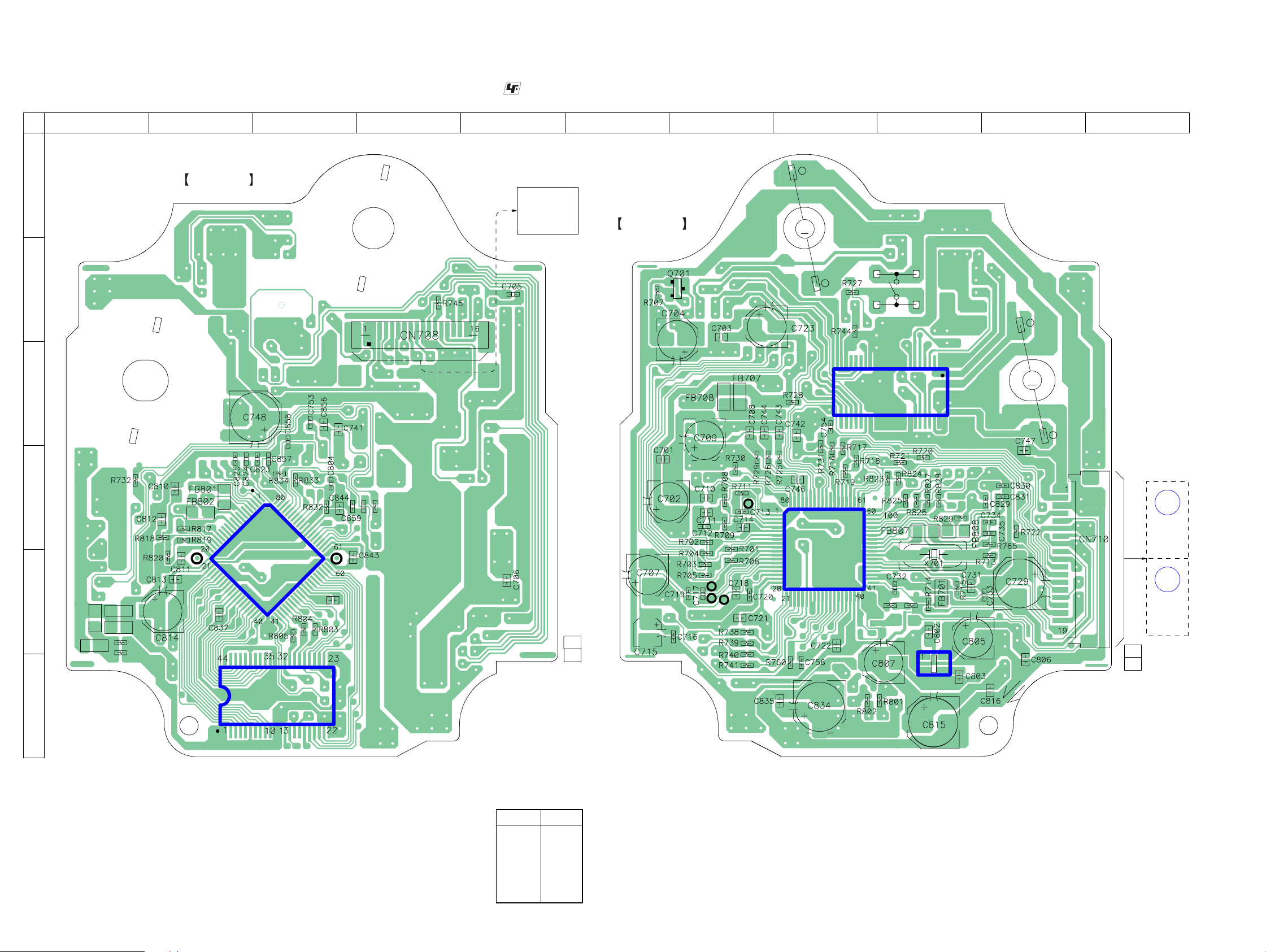
CX-JT9
6-5. PRINTED WIRING BOARD – BD Board – • See page 25 for Circuit Boards Location. :Uses unleaded solder.
1 2 3 4 5 6 7 8 9 10 11
A
BD BOARD
(COMPONENT SIDE)
OPTICAL
PICK-UP
BLOCK
(KSM-213DCP)
BD BOARD
(CONDUCTOR SIDE)
B
+
M
B
C
E
M702
(SPINDLE)
–
S701
(LIMIT IN)
+
C
D
E
F
FB806
FB805
FB803
FB804
R806
R807
IC801
IC802
C817
C860
R860
1-688-077-
11
(11)
TP
(FE)
TP
(VC)
TP
(TE)
TP
(RF)
IC721
IC722
R747 R746
7114 8
22 2815 21
34
IC803
M701
M
(SLED)
–
(SUFFIX-11)
A1
MAIN
BOARD
CN321
(Page 34)
A2
MAIN
BOARD
CN321
(Page 35)
(SUFFIX-13)
5
1-688-077-
11
(11)
• Semiconductor Location
Ref. No. Location
IC721 D-8
IC722 C-9
IC801 E-3
IC802 F-3
IC803 F-9
Q701 B-7
2626
Page 27
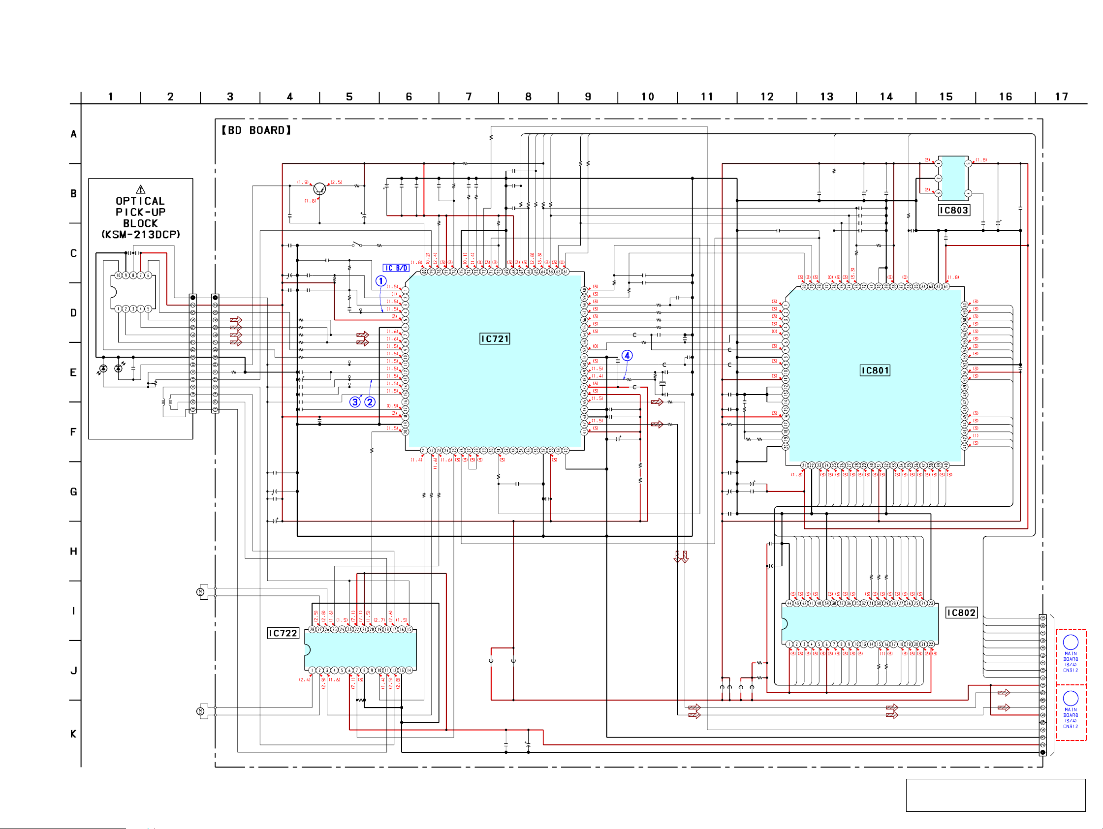
6-6. SCHEMATIC DIAGRAM – BD Board – • See page 52 for IC Block Diagrams. • See page 52 for Waveforms.
CX-JT9
R732
F
0
R
R731
2.2k
R707
10
C709
C746 C708 R729
100
0.1 0.1 12k
0.0047
6.3V
C704
47
6.3V
R727C703
1000.1
S701
R708C710
10k0.047
TP
(RF)
TP
(VC)
TP
(FE)
TP
(TE)
R738
6.8k
SLCO
SLCIST
EFMIN
RF
RFVDD
RFVSS
FIN1
FIN2
TIN1
TIN2
VREF
REF1
FE
TEC
TE
RFMON
JITTC
ADAVDD
ADAVSS
TDO
R730
1.2k
D
D
L
O
FD
0
R739
Q701
UP0411600SO
AUTOMATIC
C705
0.001
C723
100
6.3V
F
C
E
C
C
D
C
V
N
V
G
C
D
A
B
N
(LD)(PD)
CN708
16P
VC
VCC
E
D
A
B
C
F
GND
LD
VR
PD
F+
T-
T+
F-
100
R745
C714
0.1
C701
0.1
C702
100
6.3V
C706
0.1
POWER
CONTROL
(LIMIT IN)
C711
0.1
C712
47p
R702
15k
R703
R704
R705
R701
R706
C716
C715
C717
C718
C719
C720
15k
15k
15k
47k
47k
0.0047
1
0.0047
100p
0.001
1 50V
R709
27k
R711
330
C713
0.1
C721
C744
1
C743
0.047
R725R726
680680
R728
47k
E
1
T
2
S
LD
O
D
P
S
6.8k
R740
S
D
FR
D
V
V
C
A
O
D
D
P
L
S
G
0
R741
T
O
O
S
IS
U
V
D
D
K
V
P
P
M
C
_
P
D
C
RF AMP,
FOCUS/TRACKING ERROR AMP,
DIGITAL SIGNAL PROCESSOR,
DIGITAL SERVO PROCESSOR,
DIGITAL FILTER,D/A CONVERTER
LC78646E-E
6
T
N
O
S
T
E
4
/FG
/C
C
T
K
K
3R
N
C
C
P
EFE
O
B
B
D
M
C
S
S
R760
100
D
C753
47p
C754C742
47p0.1
C741
0.1
5
S
W
T2
D
S
N
V
D
O
V
IT S
C
IM
L
IC721
I1
I2
Q
N
N
P
E
O
O
/*
M
M
FS
V
C756
47p
I
S
O
Q
D
E
D
R
R
W
_
_
D
D
C
C
100
100
100
100
R718
R719
R716
R717
F
S
O
Q
R
E
D
R
D
R
W
*
*
I5
I4
I3
N
N
N
S
O
O
O
S
V
M
M
M
C722
0.1
L
E
C
C
_
D
C
R722
R721
1k
100
100
R720
1
C856
C823
I
L
E
D
C
C
DATA
DATACK
LRSY
ASDFIN
ASDACK
ASLRCK
16MOUT
EFLG
C2F
XVSS
FSX/16MIN
XIN
XOUT
XVDD
RVDD
RCHO
RVSS
LVSS
LCHO
LVDD
T
U
D
O
D
TEST
D
V
R823
100
47p
C824
R824
100
47p
FB808
C731
R829
100
0.1
R713
FB701
0.01
C733
0.01
C732
C729
220
10V
R747
33
R746
33
R825
100
R826
R827
R828
C830
C829
FB807
1M 15p
R765 C734
1k
16.9344MHz
R715
100
R714
100
C825
47p
100
100
100
22p
47p
C831
22p
X701
18p
C735
FB801
FB802
C811
0.1
C812
C810
1
0.1
R818
150
R817
3.3k
R819R820
1k1k
C816
0.1
C814
100
6.3V
C815
220
10V
C813
0.1
C837
0.1
DATACK
LRSY
ADDATA
ADBCK
ADLRCK
C2FIN
TEST1
CKIN
VSS
CKOUT
TEST2
DVDD1
PW
SBSY
SFSY
SBCK
AVDD
VPRFR
VCOC
VPDO
AVSS
DVDD2
E
C
_
3
P
M
R834
100
C807
5
I/O
100
6.3V
IN
D
M
C
4
TA
A
D
M
R833 R832
100 2.2k
T
U
O
D
CM
MP3 DECODER
A5
T
DA
M
6
7
I/O
I/O
C804
C859
C858
C857
F
V
O
IC801
LC78684E-E
6
A
AT
D
M
8
I/O
C802
0.1
22p
22p
22p
22p
K
O
T
CN
7
TA
A
D
M
C844
0.1
L
B
IN
TB
C
CE
S
A
E
T
IN
R
A
D
3
2
1
0
A
A
A
A
T
T
T
AT
A
A
A
S
VS
D
D
D
D
M
M
M
M
1
2
3
4
I/O
I/O
I/O
I/O
C
N
SY
F
R860
100
C860
100p
F
T
6
C
K
S
C
A
D
S
N
O
R
V
W
3
D
D
V
D
TD
C
VD
S
FSY
D
0
9
8
A11
A1
A
A
T
AT
AT
AT
S
D
D
DA
D
S
M
M
M
M
V
0
1
2
9
1
1
1
I/O
I/O
I/O
I/O
K
TC
S
12
A
AT
D
M
13
I/O
+1.8V REGULATOR
S
Q
E
VS
TR
S
MADRS10
MADRS11
MADRS12
13
14
A
A
AT
AT
D
D
M
M
5
14
1
I/O
I/O
IC803
MM1571J
VIN
GND
CONT
C843
DVDD5
MADRS0
MADRS1
MADRS2
MADRS3
MADRS4
MADRS5
MADRS6
MADRS7
DVDD4
MADRS8
MADRS9
CASUB
CASLB
RASB
MDATA15
6
1
I/O
VO
NOISE
C806
0.1
C805
C803
100
0.01
6.3V
0.1
A0
A1
A2
A3
A4
A5
A6
0.1
A7
VSS
OEB
WEB
C817
A8
OE
UCAS
LCAS
WE
RAS
M701
(SLED)
M702
(SPINDLE)
C707
100
6.3V
SLED/SPINDLE
MOTOR DRIVE,
FOCUS/TRACKING
COIL DRIVE
IC722
BA5836FP
S
A
C
L
100
R805
9
C
N
I/O
8
NC
I/O
R801 R802
100 100
E
S
O
A
C
U
100
100
R804
R803
S
AS
C
CA
L
U
E
C
N
W
S
E
A
R
W
C835
0.1
C834
220
10V
)
4
S
C
D
(+
N
4(-)
4
G
O
O
V
V
)
(+
(-)
1
1
O
O
V
V
C
C
C
LIN
IN
IA
V
V
S
B
T
U
O
-B
ET
TE
IN
SP
D
G
U
E
N
EG
ES
M
R
G
R
R
R744
100k
T
3
IN
T
2
IN
P
(-)
E
(+)
O
IN
3(-)
3
IN
ES
O
V
R
VO
T
)
U
(+
(-)
D
2
2
IN
FO
O
P
N
O
O
V
V
O
G
FB707FB708
FB804
C748
C747
220
0.1
10V
FB803
FB805
R807
100
R806
100
FB806
6
1
1
1
1
I/O
I/O
I/O
I/O
5
4
1
1
16
SS
V
I/O
I/O
I/O
2
3
1
C
I/O
I/O
I/O
VC
1
2
3
4
I/O
I/O
I/O
I/O
1
1
1
I/O
I/O
I/O
I/O
2
1
0
S
1
1
1
13
S
V
I/O
I/O
I/O
I/O
7
6
5
4
C
I/O
I/O
I/O
VC
I/O
5
6
7
8
I/O
I/O
I/O
I/O
9
0
1
2
3
4
5
5
7
6
8
A
E
O
S
A
R
A4
A
A
A
CN710
CD_WRQ
MP3_CE
CD_RES
AMUTE
P+7.0V
CD_CE
FSYNC
A-GND
D.OUT
D-GND
P-GND
19P
DRF
3.3V
R-CH
L-CH
3.3V
(SUFFIX-11)
CL
DO
DI
A1
(Page 32)
A2
(Page 38)
(SUFFIX-13)
5
6
7
A
A8
C
0
A
N
0
A
S
A4
A
A
VS
MEMORY
IC802
LC32V4265CT
CC
3
1
V
A
A2
A
1
2
3
A
A
A
CD_CE
DRF
CD_WRQ
-25
FSYNC
MP3_CE
CL
DO
DI
CD_RES
The components identified by mark 0 or dotted
line with mark 0 are critical for safety.
2727
Replace only with part number specified.
Page 28

CX-JT9
6-7. PRINTED WIRING BOARDS – CHANGER Section – • See page 25 for Circuit Boards Location. :Uses unleaded solder.
SENSOR BOARD
IC731
CN731
13
CN741
1-687-132-
MOTOR (LD) BOARD
SW BOARD
AK
EC
11
(11)
MOTOR (TB) BOARD
M741
(TABLE)
M
CLOSE
OPEN
CN751
1
2
S751
OPEN/CLOSE
DETECT
1-687-669-
1-687-134-
CN742
11
(11)
11
(11)
DRIVER BOARD
Q731
R733
C737
E
C736
CN705
2
1
CN702
C751
CN704
2
R732
R734
R735
C735
R751
C741
JW710
R723
1
JW711
R722
CN703
C752
JW712
JW708
JW709
R721
D711
R701
D701
R702
4
JW707
C715
JW706
JW705
R713
(SUFFIX-11) (SUFFIX-13)
MAIN BOARD
B1
CN309
(Page 34) (Page 35)
CN701
19
R711
R712
19
JW713
B2
JW704
JW714
MAIN BOARD
CN309
JW702
JW703
IC712
IC701
C731
R731
JW701
1-687-135-
11
(11)
M751
(LOADING)
M
CN721
2
1
1-687-133-
S711
ROTARY ENCODER
DISC TRAY
ADDRESS DETECT
11
(11)
2828
Page 29

6-8. SCHEMATIC DIAGRAM – CHANGER Section – • See page 52 for IC Block Diagrams.
LOADING MOTOR
DRIVE
IC701
BA6956AN
VREF
OUT2
OUT1
CX-JT9
VCC
FIN
VM
GND
RIN
IC731
RPI-576
TABLE ADDRESS SENSOR
M741
(TABLE)
SENS-IN
SENS-OUT
CN731
GND
CN721
2P
M751
(LOADING)
S711
DISC TRAY
ADDRESS DETECT
E3
E2
E1
CN741
3P
3P
SENS-IN
SENS-OUT
GND
S751
OPEN/CLOSE
DETECT
OPEN
CLOSE
LM-2
LM-1 LM-1
CN742 CN702
5P 5P
TM-2
TM-1
SENS-IN
SENS-OUT
GND
CN751 CN705
2P 2P
OPEN SW OPEN SW
GND GND
CN704
2P
LM-2
CN703
4P
E-3
E-2
E-1
GND
TM-2
TM-1
SENS-IN
SENS-OUT
GND
0.1
C735
0.1
C736
0.1
C737
R735
4.7k
R723
100
4.7k
R722
4.7k
R721
C751
0.01
D711
MTZJ-T-77
3.6B
R734
12k
R733
1k
TABLE MOTOR
DRIVE
IC712
BA6956AN
R702 R701
100 470
D701
MTZJ-T-77
5.1A
R712 R711
4.7k 1k
R713
22k
VREF
DTC114ESA
OUT2
R731R732
C741
0.01
10010k
Q731
LEVEL
SHIFT
RNF RNF
OUT1
VCC
FIN
VM
GND
RIN
C715
100
16V
TBL ADDRESS SENS
M+9V
LM-R
TM-R
D+3.3V
OPEN SW
GND
LM-F
TM-F
CN701
12P
E-1
E-2
E-3
(SUFFIX-11)
B1
(Page 31)
B2
(Page 37)
(SUFFIX-13)
C731
10
50V
C752 R751
0.1 4.7k
2929
Page 30

CX-JT9
6-9. SCHEMATIC DIAGRAM – MAIN Board (1/4) (Suffix-11) – • See page 52 for IC Block Diagram.
(1/4)
CN101
11P
ANTENNA
(COAXIAL)
CLK
DO
DI
CE
JK302
VM+9V
TUNED
ST
TUNER-L
GND
TUNER-R
TU-MUTE
2P
R301
4.7k
R302
4.7k
TUNER UNIT
SUPPLIED WITH
AM
LOOP
THE ASSEMBLED
BLOCK
MD(VIDEO)
IN
L
R
D102
C103
R101
R102
R304 R303
22k 22k
JR300 C300
01
10EDB40-TB3
100 16V
10k
10k
C351
CLK
DO
DI
CE
TUNED
C101
C310
4.7
ST
TUMUTE
C102
4.7
50V
470p
C352
470p
10
50V
50V
10
50V
10 50V
C301
10k
R330
A1
A2
A4
C309
10
50V
10 50V
C311C312
C365
220p
C411
4.7
35V
C313
10
16V
C327
0.0027
C317
R317
10
2.2k
50V
R325
0.022
C321
10k
0.022
C325C319
0.0470.047
C323
JR313JR312
00
R321 JR325
15k 0
1k
0.22
0.22
C331
C361
220p
R319
C333
1000p
C357
C356
1000
470p
10V
R324
C354
1k
MCLK
-VFL
R380
470k
R397
10k
Q311 Q310
R355 R356
2SD1306 2SD1306
2.2k 2.2k
C342 R354 R358R399 R398
0.1 47k 22k5.6k 5.6k
MUTINGMUTING
Q312
2SA1235F
MUTING
CONTROL
SWITCH
CD-MUTE
2.2k
R395
R316
10k
A5
2.2k
R396
(Page 31)
2
INPUT SELECT SWITCH,
TONE CONTROL,
ELECTRICAL VOLUME,
BASS BOOST AMP
IC301
M61529FP
C304
R327
4.7k
MIC-SIG
220p
C366
B1
B2
B3
4.7
50V
L2
P
PL1
/D
2
1/D
R
UR
U
S
S
IC
EF
R
M
C303
C353
100
470p
10V
-R
D
C
C302
10 50V
-L
-L
-L
D-L
ER
C
N
TU
-R
ER
N
TU
4.7
35V
E-L
D
PE
M
M
A
TA
G
-R
E
-R
M
D
A
APE-R
T
M
G
C314C412
10
16V
2
I2
-2
B
EC
R
B-1
EC
R
A2
O
TM
TC
TCB2
TM
1
O
I1
A1
M
TM
T
TC
TCB1
0.022
0.022
C320
R318
2.2k
0.0027
C326
0.047
C324
C328
R326
10k
C318
10
50V
2
T2
CC
T
1
C
TC
_A2
U
LIN
BB
TO
VO
1
T1
LIN
U
O
B-A1
TO
V
B
0.22
0.22
C334
C332
0
0
JR311
JR310
R322
15k
JR322
B5
B4
T
D
T2
U
CK
N
U
O
O
B_B2
B
B-B1
B
R320
1k
0
G
O
W
CL
S
UT
C
UT1
O
ATA
AO
S
VC
D
D317
C337
10
50V
R328
R323
33k
1k
R
T
/S
S
C
I
A
D
V
1SS355
C355
470p
C362
220p
C393
0.47
50V
R365
1M
B6
B7
B8
B9
B10
A6
A7
C1
C2
C3
C4
C5
(Page 33)
(Page 32)
3030
Page 31

6-10. SCHEMATIC DIAGRAM – MAIN Board (2/4) (Suffix-11) – • See page 52 for IC Block Diagram. • See page 52 for Waveforms.
C268
1
R266
C273
1 50V
C272
1 50V
NC
ALC(L)
ALC(R)
HA12237F
REC-IN(L)
C247
2.2
50V
R271
10k
C248
2.2
50V
REC-IN(R)
IC201
NC
50V
NC
PB-OUT(L)
C269
1
50V
PB-OUT(R)
TAI(L)
TAI(R)
EQOUT(L)
C267
0.01
R265
4.7k
R267
4.7k
4.7k
C266
0.01
EQOUT(R)
PB-NF2(L)
PB-EQ(L)
PB-NF2
(R)
PB-EQ(R)
PB-NF1(R)
REC-RETURN
PB-NF1(L)
R220
10k
AIN(R)
NC
BIN(R)
GND
BIN(L)
RIP
AIN(L)
DECK A/B SELECT SWITCH,
REC/PB EQ AMP
(Page 30)
(2/4)
R286
R216
A1
A2
A4
A5
R232R234
C234
2.2k22k
1000p
C286
2200p
R226 C226
10k 2200p
R233
22k
C253
10k
C259
22
25V
R235
D205
10k
1SS355
R270R282
10k100
C254
R284
R283
100
16V
R231
2.2k
R225
4.7
10k
10k
50V
C233
1000p
10k
4.7k
R287R288
10k10k
C258
4.7
50V
R278
22k
C285 R285
2200p 10k
C225
2200p
R272
10k
C260
0.47 50V
C250
2.2
50V
REC-OUT(R)
NOR
VCC
ALC-DET
GND
IREF
TEST
REC-OUT
(L)
C261
0.47
50V
R215
4.7k
OFFALC-ON/
/HI
BA/
OFFMUTE-ON/
ONRECMUTE- /OFF
NC
C249
2.2
50V
CX-JT9
R268
4.7k
CN203
3P
1000p
1000p
C202
1000p
C201
1000p
C204
C203
CN202
8P
C232
47
16V
C237
1 50V
C244
47 16V
HP1
(PB)
(DECK-A)
HPRE1
(REC/PB/ERASE)
(DECK-B)
L-CH
R-CH
R-CH
L-CH
ERASE
Q223
2SC2001
BIAS OSC
R251
4.7
A6
A7
R400 R401 R402 R404 R405
10k 10k 10k 10k 10k
E2
E1
C239
0.015
C242C241
0.00470.0047
R252
22k
CLK
LCK
R368
100
R307
100
R430
10k
L201
BIAS OSC
S-OUT
R485
100
C392 C391 C390
100p 100p 100p
MULTI CONTROLLER
BU2099FV
VSS
NC
DATA
CLOCK
LCK
REC
BIAS
B
A/
PB MUTE
REC MUTE
IC309
REAR SP
FRONT SP
E3
TM-L(CD)
TM-R(CD)
LM-L(CD)
LM-R(CD)
TUNER
C223
0.022
100V
R241 R242
4.7k 4.7k
SP-F
LINK
C401
0.1
VDD
OE
SO
ON
/OFF
ON
OFF
/
MUTE
R486
100
R407 R408 R409 R410
10k 10k 10k 10k
MUTING MUTING
Q221 Q218
2SC3052F 2SC3052F
MUTING
R420
10k
R412 R413
10k 10k
2SC3052F2SC3052F
1SS355
VSS
NC
DATA
CLOCK
LCK
NC
NC
NC
I-BASS
CTRL3
D305
MUTING
Q220Q219
IC310
BU2099FV
BB CTRL1
BB CTRL2
BB CTRL3
BB CTRL4
CTRL1
CTRL2
Q222
2SC3052F
VDD
OE
SO
NC
Q225
2SA1235F
Q222,225
R245R273
REC ON/OFF
10k10k
SWITCH
C221
47
16V
BASS BOOST CONTROLLER
D206
1SS355
R246
47k
C402
0.1
CD-EN
TBL-SENSE
1SS355
R260
220
C240
10
50V
D306
R418R417R416R415R419 R414
10k10k10k10k10k 10k
Q228
2SB1116
REC BIAS
SWITCH
R269
10k
R253
10k
D+3.3V
(CHASSIS)
CN309
12P
M+9V
GND
LM-R
LM-F
TM-R
TM-F
E-1
E-2
E-3
(Page 29)
GA1
C450
10
50V
R424
22k
R353
R352
R455
R466
JR309
R425
11k
11k
11k
22k
0
JR308
JR307
JR306
JR305
JR304
JR303
JR316
22k
R426
22k
R406
22k
24
23
0
22
0
21
0
20
0
19
0
18
0
V-BASS
0
TUMUTE
TBL ADDRESS SENS
OPEN SW
(Page 33)
3131
Page 32

CX-JT9
6-11. SCHEMATIC DIAGRAM – MAIN Board (3/4) (Suffix-11) – • See page 52 for IC Block Diagram.
B4
(3/4)
B2
B1
B3
(Page 30)
B7
B8
B5
B6
B9
B10
F1
F2
F3
(Page 42)
(Page 45)
M731
(FAN)
(Page 27)
CN306
13P
L-OUT
SP-GND
R-OUT
LINK/MATRIX
UNREG VM
RELAY B+
IN-L
A-GND
IN-R
VCC
PW-GND
VM(AC)
VM(AC)
CN310
5P
HP CTL
D GND
R-OUT
HP-GND
L-OUT
CN303
3P
FAN+
FAN-
FAN+
CN312
19P
P-GND
P+7.0V
D-GND
AMUTE
D.OUT
3.3V
L-CH
A-GND
R-CH
3.3V
CD_RES
DI
DO
CL
MP3_CE
FSYNC
CD_WRQ
DRF
CD_CE
JR336
4.7k
R375
5.6k
R340
R347
4.7
4.7k
50V
LINK
C329
4.7
50V
R492
220k
R491
220k
Q491
2SC3052F
FEED BACK
HP
R394
10
JR333
0
ZZ1
ZZ2
ZZ3
ZZ4
ZZ5
ZZ6
ZZ7
ZZ8
0
2SA1980G
C386
47
25V
JR339
JR341
C315
R493 C491
4.7
100k 0.015
50V
Q327
2SA1235F
R315 Q372
10k 2SC3052F
Q328
0
0
SWITCH
R393
R470
3.3k
R392
220
FAN MOTOR ON/OFF SWITCH
R494
220k
10k
Q327,328,372,373
C492
1
50V
D372 D371
1SS355 1SS355
R359
470k
C379 C377
R391
47
47k
25V
Q492
2SK2158
BASS BOOST
CONTROL
D374
1SS355
4.7
50V
R495
22k
C382
3300p
INB
HINA
INA
C383
3300p
Q373
R371
4.7k
R372
4.7k
2SC2001LK
C398
10
50V
C330C316
4.7
50V
C384
0.033
LINB
HINB
HOUTB
HOUTA
LINA
C385
0.033
LOUTA
LOUTB
VREF
OUTB
OUTA
BBE
R335
C367
0.22
R461R460
2.2k2.2k
UDZSTE-1713B
C340
R338
47
4.7k
16V
GIN
GND
GOUT
LPOUT
LPIN
V+
56k
C396
0.22
R421
10k
D312
BASS BOOST
ENHANCER
IC303
NJM2156
R480
10k
Q314
2SK2541
Q314-316
FERQUENCY
CONTROL
18 19 20
R468
82k
R332
47k
R300
4.7k
C341
47
16V
Q304
2SA953K
FRONT
SPEAKER
ON/OFF
RELAY
DRIVE
R339
1k
R403
820
Q315
2SK2541
R333
10k
Q317
2SK2541
C400
22
25V
R361
5.6k
R362
22k
R479 R337 R467
47k 1.5k 1.5k
R334
8.2k
Q318
2SK2541
Q317-320
BASS BOOST
CONTROL
2SC3052
BASS BOOST ON/OFF SWITCH
R433
680
2W
C439
4.7 100V
R370
Q323
R434
680
R363
22k
Q316
2SK2541
JR337
0
Q319
2SK2541
Q320
2SK2541
10k
R367
4.7k
R366
270
2W
C440
4.7
100V
3.3k
R331
2.2k
R478
R336
27k
21
22
50V
50V
10
10
C369
C370
F4
(Page 33)
F5
F6
F7
F8
F9
V-BASS
CD-MUTE
23
24
R364
100k
D311
1SS355
SP-F
(Page 47)
CN311
9P
LC78646 CE
CD DRF
LC78646 WRQ
LC78684 SYNC
LC78684 CE(MP3)
LC78646/LC78684 CLK
LC78646/LC78684 DO
LC78646/LC78684 DI
LC78646 RESET
ZZ8
ZZ7
ZZ6
ZZ5
ZZ4
ZZ2
ZZ3
ZZ1
F10
The components identified by mark 0 or dotted
line with mark 0 are critical for safety.
3232
Replace only with part number specified.
Page 33

6-12. SCHEMATIC DIAGRAM – MAIN Board (4/4) (Suffix-11) –
(Page 30) (Page 31)
4
2
3
5
C
C
C
C363
10
50V
R432
100
C339
220
16V
D304D303
C374C373
0.010.01
(Page 32)
C
(4/4)
F1
F2
GND
F3
F4
D319 D320
F5
F6
F7
F8
F9
10EDB40-TB3 10EDB40-TB3
D321 D322
10EDB40-TB3 10EDB40-TB3
R310
R309
0
BUFFER
C419C418
0.010.01
IC304
NJM4565M
C364
10
50V
10EDB40-TB310EDB40-TB3
D301 D302
10EDB40-TB3 10EDB40-TB3
C417
1000
10V
VCC
0
CX-JT9
1
C
R314
100k
R427 R428
00
R487
0
R488
0
C375
2200
25V
+9V REGULATOR +9V REGULATOR +10V REGULATOR+4V REGULATOR
IC305 IC306 IC308 IC313
TA7809S TA7809S TA7810S
IO
G
JR302
0
D315 D313
10EDB40-TB3 10EDB40-TB3
D307
1SS355
10EDB40-TB3
R484
10k
Q330
2SC3052F
1
E
E2
R313
100k
C380 C381
470
16V
D314
Q331
2SA1235F
10EDB40-TB3
R483
1k
POWER ON/OFF
R482 R481
4.7k 4.7k
µPC3504HF
IO
D316
Q330,331
RELAY DRIVE
E3
MIC10V
CN304
0
0
0
22k
SW ON/OFF SENS
SW LIMIT
O-POWER
SYSTEM MUTE
VSTBY
SW OUT
VM+10V
DC-DET
HOLD
FIL-1
FIL-2
CN307
P-0N
-VFL
31P
13P
VF1
VF2
D-GND
-VFL
EVER 10V
MIC 10V
4V(SW)
BU1924 CLK
BU1924 DATA
TUNER STEREO
TUNER TUNED
LC72121 CE
LC72121 DI
LC72121/M61529/BU2099FV DO
LC72121/BU2099FV CLK
M61529 CLK
BU2099FB LCK
CD NUMBER SENS
BU UP DOWN/CD OPEN CLOSE
NC
SYSTEM MUTE
STREAM IN(VACS)
TUNER S-METER
S-OUT
DECK 9V
MIC GND
MIC SIG
PROTECTOR (HOLDER)
POWER RELAY
HP
A-GND
(Page 42)
(Page 47)
FIL2
FIL1
-VFL
EVER+10V
MIC+10V
+4V
ST
TUNED
CE
DO
DI
CLK
MCLK
LCK
TBL-SENSE
CD-EN
S-MUTE
VACS/STR
S-OUT
DECK+9V
JR326
R386
R387
0
MIC-S
HOLD
O-POWER
HP
FIL1
FIL2
10k
12k
EVER+10V
-VFL
O-POWER
HOLD
S-MUTE
IO
G
47
16V
G
C399
470
16V
C371
47
16V
R378
10k
R379
2.2k
C420 C421
2200
25V
Q301
2SA1980G
Q301,302
B+ SWITCH
Q302
2SC3052F
C372
10
50V
IO
G
220
16V
Q324
355
S
150k
1S
4
31
4
36
R
D
C345
100
16V
2SC3052F
CENTER
VOLTAGE
GENERATOR
R388
1k
C397
100
10V
R348 R384
01k
JR317
JR321
JR328
R346
D308
0
F10
O-POWER
DECK+9V
+4V
O-POWER
JR334
MIC-SIG
0
MIC-S
3333
Page 34

CX-JT9
6-13. PRINTED WIRING BOARD – MAIN Board (Suffix-11) – • See page 25 for Circuit Boards Location. :Uses unleaded solder.
• Semiconductor
Location
Ref. No. Location
D102 C-16
D205 M-6
D206 N-8
D301 O-13
D302 N-13
D303 O-13
D304 N-13
D305 G-6
D306 E-10
D307 O-11
D311 P-15
D312 L-15
D313 F-8
D314 F-9
D315 E-10
D316 J-11
D317 H-16
D319 O-14
D320 N-15
D321 O-14
D322 N-14
D364 O-12
D371 O-15
D372 P-15
D374 O-15
IC201 L-6
IC301 G-13
IC303 G-9
IC304 K-14
IC305 N-13
IC306 N-12
IC308 N-11
IC309 F-6
IC310 F-5
IC313 N-14
Q218 L-5
Q219 L-4
Q220 L-4
Q221 L-4
Q222 O-6
Q223 N-5
Q225 O-7
Q228 O-6
Q301 O-12
Q302 O-11
Q304 O-15
Q310 F-10
Q311 F-10
Q312 F-9
Q314 D-6
Q315 D-7
Q316 D-7
Q317 D-6
Q318 D-6
Q319 D-5
Q320 D-5
Q323 F-8
Q324 L-13
Q327 O-16
Q328 N-16
Q330 O-10
Q331 O-10
Q372 P-16
Q373 M-15
Q491 H-8
Q492 G-8
1 2 3 4 5 6 7 8 9 10 11 12 13 14 15 16 17
A
JW409
JW205
(Page 46)
PANEL BOARD
E1
CN701
JW270
19
CN311
28
R333
R334
R479
R467
R337
R380
Q319
Q318
Q320
R367
JR308
R415
JR316
JR309
R414
C392
R307
JR326
JR328
R384
JW202
Q220
E
Q219
E
9
JW238
JW275
C226
R368
Q221
E
JW200
R220
C402
C390
JW428
JW432
R419
R412
JW429
JW437
31
CN203
C202
JW203
Q218
E
JW204
JW278
R241
C232
R266
R226
R268
R225
1
C239
JW237
R251
C240
S
S
S
D
D
G
G
G
JR306
JR307
R417
R416
R418
JW441
IC310
R413
JW442
JW434
JW433
JW439
JW438
JW484
JW485
JW486
C244
C201
C203
C237
31 30
IC201
C204
40 21
120
10 11
C266
C272
C268
C248
C260
R272
JW252
R286
C241
C225
R252
E
R260
Q223
R253
R339
R336
R331
R403
R410
JW446
JW474
JW475
JW476
C273
C221
S
R340
G
IC309
C391
R420
JW482
JW483
JW447
JW206
R278
C258
D205
R235
E
R478
R375
Q316
Q315
S
S
JW272
D
D
D
JW271
G
G
JW453
JW454
JW450
R409
R408
R407
R405
R430
JW458
R402
R404
R401
R400
JW469
JW471
R366
JW478
JW276
JW492
JW207
R231
C285
R215
C233
R285
R265
C269
JW214
C259
Q222
JW236
JW211
R267
C261
C253
R282
C254
R284
R283
R287
JW227
R270
R288
R234
R232
C234
JW234
R273
E
R245
Q225
JW411
R332
Q317
R468
Q314
S
D
D
G
JR337
JR304
JW415
R486
JR303
JR305
C401
JW444
JW445
JW443
R436
D305
JW472
JW473
JW487
JW488
JW489
JW490
JW491
R271
C247
C267
C250
R216
JW235
C286
C242
Q228
E
R269
JW455
Q492
JW226
C249
JW440
JW459
JW461
JW263
C492
JW213
D206
R246
JW468
JW212
JW499
JW209
Q323
JW493
JW449
JW466
JW467
S
G
R494
JW462
D
JW210
JW225
R353
R352
R495
E
Q491
JW494
JW269
R455
C450
E
JW448
R300
R370
R233
DRIVER BOARD
B1
CN701
JW452
R406
R424
R425
R426
D306
JW457
CN309
1
R466
JR339
R316
D314
Q312
D313
E
C367
C396
R335
R491
JW479
C329
R347
IC303
R338
C341
C384
C340
JW481
C309
JW217
C411
JW216
JW218
JW219
JW224
JW232
JW251
C400
C491
R493
JW463
12
Q311
R355
R358
E
R354
R397
C342
C383
C385
R492
C330
110
JW265
2011
C382
C316
JW356
JW358
JW273
JW220
JW221
JW268
JW222
JW223
JW231
R481
R483
E
Q330
E
Q331
R482
JR334
(Page 26)(Page 28)
BD BOARD
A1
CN710
JW337
1
D315
Q310
E
R356
JW357
JR300
C310
JW372
JW373
IC308
C371
R484
2
C399
JW350
CN312
JW338
JW347
R399
JW267
JW330
JW354
JW355
JW371
C417
D307
JW341
JW460
R398
C366
JW398
Q302
R431
D308
R396
JW348
C365
C380
C313
JW359
JW361
C370
JW346
C311
JW335
JW368
IC306
C381
Q301
E
D364
JR341
C369
R395
C315
R327
C312
C304
C300
JW470
JW392
C372
R379
R378
CN307
JW112
19
18
JW342
JW344
JW345
C319
42 22
JR311
JR310
JW333
JW332
JW331
JW329
C353
C320
C324
JW362
JW363
D316
R387
R388
JW277
JW383
JW385
JW253
C375
JW320
JR302
JW389
D302
JW360
JW370
C374
JW380
E
C373
JW430
JW397
131
B
MAIN BOARD
C
JW404
JW405
JW406
JR317
CN304
2
30
JW407
JW408
1
JW426
R485
JR321
JW427
31
D
E
F1
PANEL
BOARD
F
CN101
(Page 46)
G
JW417
JW274
JW416
JW419
JW421
JW279
JW418
JW422
JW423
JW424
H
JW498
JW495
JW496
JW497
JW436
R346
R348
JW201
CN202
8
1
R242
JW239
L201
BIAS OSC
C223
CLP3
JW435
I
J
K
L
HP1
(PB)
(DECK-A)
HRPE1
(REC/PB/ERASE)
(DECK-B)
C440
C439
R433
R434
M
D1
N
HEADPHONE
BOARD
CN105
CN310
15
(Page 44)
CLP2
O
P
JW456
ANTENNA
FM 75Ω
TUNER UNIT
CN101
2
JW103
R101
C102
JW107
JW108
R317
C323
JR312
AM
LOOP
JW102
11
10
R102
JW106
C333
C327
C331
C317
R319
JR313
R321
C361
JR325
C354
(COAXIAL)
SUPPLIED WITH THE
ASSEMBLED BLOCK
1
JW109
C101
C321
R325
C325
R330
IC301
C357
121
JW328
C326
C303
R326
R318
C318
C412
JW365
C397
JW382
C345
E
Q324
JW340
R428
W1
D304
D303
D301
JW420
C355
C356
JW308
C334
JR322
R322
R320
C332
C328
C314
C363
R313
C364
R314
R310
R386
JW384
JW386
R487
R427
JW300
JW387
R488
JW264
IC305
JW394
JW396
JW266
JW410
CN306
C421
JW327
JW319
JW321
JW322
C362
JW324
JW325
JW323
JW326
13
R309
IC304
R432
C339
D312
C420
W1
IC313
D322
C419
C418
D319
Q304
R372
D321
JW113
R328
31313131
D102
C103C103
R324
JW307
B
C337
CN303
R303
R365
C398
R460
E
R421
E
R371
D374
R362
R363
131
R323
JW305
D317
JW304
JW309
JW312
JW313
JW314
JW315
JW316
C302
C301
C351
C352
R304
R302
R301
C393
JR333
C386
R461
JR336
Q373
C379
D320
JW393
R391
JW395
R361
E
C377
JW400
JW390
D371
Q327
E
R393
R359
Q372
D372
E
D311
R364
GA1
Q
G1
POWER BOARD
CN502
C1
POWER BOARD
CN501
(CHASSIS)
(Page 40) (Page 40)
R394
R392
JW310
Q328
JW301
JW302
JW303
R315
R470
1-688-080-
M731
M
(FAN)
JK302
R
MD (VIDEO)
IN
L
R480
11
3434
Page 35

6-14. PRINTED WIRING BOARD – MAIN Board (Suffix-13) – • See page 25 for Circuit Boards Location. :Uses unleaded solder.
CX-JT9
1 2 3 4 5 6 7 8 9 10 11 12 13 14 15 16
A
B
C
D
E
F
G
H
I
J
K
L
M
N
O
P
F2
PANEL
BOARD
CN101
(Page 46)
HP1
(PB)
(DECK-A)
HRPE1
(REC/PB/ERASE)
(DECK-B)
D2
HEADPHONE
BOARD
CN105
(Page 44)
R433
CLP2
C440
C439
CN310
MAIN BOARD
JW416
JW417
JW418
JW274
JW419
JW421
JR317
JW422
JW423
JW424
JW435
JW498
R434
15
30
2
JW495
JW496
JW497
CN304
JW405
31
1
L201
BIAS OSC
JW403
JW407
JW436
R346
CN202
R485
JW239
C223
8
1
JW406
JW408
JR321
JW427
JW201
CLP3
JW409
JW426
R348
E
R307
R384
JW205
R498
JR326
JW238
JR316
R368
JW202
R242
E
Q220
Q219
R226
C226
9
E
R220
9
R499
JW200
Q221
1
JW428
R241
8
R367
JR309
C390
R412
JR328
C202
E
(Page 46)
PANEL BOARD
E2
CN701
1
CN311
2
R337
R380
S
D
Q320
G
R415
JR308
R416
R414
C402
IC310
R413
JW432
R419
JW429
JW433
13
CN203
C201
JW203
C203
Q218
JW204
C204
JW278
C232
C268
R266
C248
R268
R272
R225
C239
C225
Q223
JW237
R251
C240
JR307
JW434
C266
R260
R390
R467
Q319
JW438
E
JR306
R417
JW484
JW485
JW486
C272
JW270
R479
S
G
C237
C242
R253
(Page 26)(Page 28)
BD BOARD
A2
CN710
1
2
JR343
E
R356
Q310
C315
C330
JR334
JW357
JW358
JR300
C310
JW372
JW373
JW273
C399
IC308
C371
R484
G2
(Page 40) (Page 41) (Page 40) (Page 41)
(E51) (MX)
JW338
JR341
C369
R395
JW347
JW348
R327
JR314
C300
JW392
C372
JW350
R378
R379
POWER BOARD
CN502
JW339
JW470
JW460
JW341
C366
JW371
C417
JW330
C381
R398
JW354
JW267
D307
CN312
CN307
R399
D325
C448
JW346
C380
Q302
R431
D308
C313
C312
C304
JW359
JW361
D316
IC306
E
G3
C447
C370
R396
C311
JW335
JW355
JW368
JW320
Q301
D364
POWER BOARD
E
JW398
JW334
JW367
D323
JW253
CN502
R341
18
JW333
JW389
19
C358
JR311
JR310
JW380
JW342
JW343
JW362
JW363
JW364
JW370
JW344
JW345
JW332
JW277
JW430
JW112
JW331
C353
C320
R388
JW385
C375
JW360
C373
JW397
131 131
JW329
D302
JW455
C492
C249
JW440
JW499
JW459
JW461
JW263
JW212
JW213
JW226
D206
R246
JW468
Q492
R494
JW209
Q323
JW493
JW210
JW466
JW467
S
G
JW225
R352
JW462
D
R353
R300
R495
E
Q491
JW494
R455
C450
E
JW269
JW448
C396
C491
R493
R233
D313
C400
JW479
JW219
R370
JW457
R338
R347
1
JW481
R406
R466
C367
R335
C341
JW217
JW216
JW280
D314
E
Q312
C329
C340
C309
JW218
JW282
JW251
R299
JW411
R339
R478
R403
R331
R336
R408
R407
R402
R285
R265
R283
C234
JW236
S
G
JW469
D
R231
R270
R287
R400
R288
R232
Q315
Q225
S
D
G
JW450
R405
IC309
JW492
C233
R267
C253
JW234
E
JW458
C261
R282
R284
JW298
R234
R273
R430
JW272
JW271
R366
JW478
C254
JW227
R375
JW453
JW454
JW207
JW211
R333
R334
R468
R332
S
S
G
JW442
D305
C267
C260
R252
R269
D
JR305
JW441
R271
IC201
R216
Q228
Q317
JW415
JW443
JW472
JW473
C241
S
G
JR337
JR303
C250
JW235
C286
R340
D
G
D
Q316
Q314
JR304
R486
R410
R409
C401
JW444
C391
JW446
R404
JW445
R401
R420
JW471
JW474
JW475
JW482
JW483 JW276
JW487
JW488
JW489
JW490
JW491
JW206
C285
C247
R215
C273
C269
JW214
R278
C258
D205
C259
R235
Q222
R245
E
E
C221
Q318
D
R418
JW439
C244
JW252
R286
CN309
JR339
R316
C384
C411
JW283
R424
R491
DRIVER BOARD
B2
CN701
D324
R426
R425
D306
12
D315
Q311
R355
R358
E
R354
C383
R397
C342
R492
C385
IC303
JW265
C382
JW356
JW220
JW281
JW268
JW222
JW221
JW223
JW231
R481
R483
E
Q330
E
Q331
R482
JW456
ANTENNA
FM 75Ω
TUNER UNIT
CN101
2
R101
C101
JW107
JW108
R317
C323
C317
R325
JR312
C328
C332
C314
C363
R313
R314
R386
JW384
JW386
R487
R427
JW300
R428
JW264
IC305
D304
JW394
JW396
JW266
JW410
CN306
CN501
R102
JW387
LOOP
C327
JR313
JW327
R310
R432
C418
AM
JW106
JW308
R322
C334
R320
C421
10
C102
C361
C354
C362
JW326
C3
11
R321
C355
C356
R319
JR322
JW322
JW325
R309
C420
13131313
D321
JW103
C331
JR325
C357
JW319
JW321
JW324
JW323
IC304
IC313
D322
D319
R363
R372
POWER BOARD
CN501
(COAXIAL)
SUPPLIED WITH THE
ASSEMBLED BLOCK
1
C321
C325
R330
C319
42 22
IC301
121
JW328
C326
C303
R326
R318
C318
C324
C412
JW365
C397
R387
C364
JW382
C345
E
Q324
JW340
R488
C374
D303
D301
JW420
POWER BOARD
C2
(E51) (MX)
R460
D374
JW307
C337
3
R365
C398
R421
R371
C103
C352 C351
E
Q373
D320
R362
R361
JW314
JR333
R461
JW313
C301
JW393
JW395
JW315
JW316
R301
C393
C386
JW305
JR336
R391
R303
D371
R359
D311
R304
R324
R323
D102
JW304
R302
D317
C302
C377
JW400
JW390
Q327
E
Q372
D372
R364
(CHASSIS)
JW301
JW302
JW303
R329
JW309
JW310
C379
E
Q328
R394
R315
R470
R393
E
R392
GA1
1-688-080-
JW102
C333
C425
R328
1
CN303
C339
D312
C419
Q304
E
R480
• Semiconductor
Location
Ref. No. Location
D102 C-14
D205 L-6
D206 M-7
D301 N-11
D302 M-11
D303 N-12
D304 M-12
D305 G-5
D306 E-9
D307 N-10
D311 O-14
D312 K-13
D313 F-8
D314 E-8
D315 E-9
D316 I-10
D317 G-14
D319 N-13
D320 M-13
D321 N-13
D322 M-13
D324 E-9
D364 N-10
D371 N-14
D372 O-14
D374 N-13
IC201 K-5
IC301 G-12
IC303 G-8
IC304 K-13
IC305 M-12
IC306 M-11
IC308 M-10
IC309 F-6
IC310 F-5
IC313 M-13
Q218 K-4
Q219 L-4
Q220 K-4
M731
M
(FAN)
JK302
R
MD (VIDEO)
IN
L
13
Q221 L-4
Q222 N-6
Q223 M-5
Q225 N-6
Q228 N-5
Q301 M-11
Q302 M-10
Q304 N-13
Q310 F-9
Q311 E-9
Q312 F-8
Q314 D-6
Q315 D-6
Q316 D-6
Q317 D-5
Q318 D-5
Q319 D-5
Q320 D-4
Q323 F-7
Q324 K-11
Q327 N-14
Q328 M-14
Q330 N-9
Q331 N-9
Q372 N-14
Q373 L-14
Q491 G-7
Q492 G-7
3535
Page 36

CX-JT9
6-15. SCHEMATIC DIAGRAM – MAIN Board (1/4) (Suffix-13) – • See page 52 for IC Block Diagram.
(1/4)
CN101
ANTENNA
FM 75
(COAXIAL)
LOOP
11P
CLK
DO
DI
JK302
CE
VM+9V
TUNED
ST
TUNER-L
GND
TUNER-R
TU-MUTE
2P
R301
4.7k
R302
4.7k
D102
C103
R101
R102
R304 R303
22k 22k
JR300 C300
01
Ω
AM
TUNER UNIT
SUPPLIED WITH
THE ASSEMBLED
BLOCK
MD(VIDEO)
IN
L
R
100 16V
10k
10k
C351
10EDB40-TB3
TUMUTE
470p
TUNED
CLK
DO
DI
CE
C310
C101
ST
C102
4.7
50V
C352
470p
10
4.7
50V
50V
10
50V
C301
10 50V
10k
R330
A1
A2
A4
C309
10
50V
10 50V
C311C312
C365
220p
C411
4.7
35V
C313
10
16V
C327
0.0027
C317
R317
10
2.2k
50V
R325
0.022
C321
10k
0.022
C325C319
0.0470.047
C323
JR313JR312
00
R321 JR325
15k 0
1k
0.22
0.22
C361
220p
R319
C331
C333
1000p
C357
C356
1000
470p
10V
C354
R324
1k
MCLK
-VFL
R380
470k
R397
10k
R355 R356
Q311 Q310
2.2k 2.2k
2SD1306 2SD1306
C342 R354 R358
0.1 47k 22k
MUTINGMUTING
R399 R398
5.6k 5.6k
Q312
2SA1235F
MUTING
CONTROL
SWITCH
CD-MUTE
2.2k
R395
R316
10k
A5
2.2k
R396
(Page 37)
2
INPUT SELECT SWITCH,
TONE CONTROL,
ELECTRICAL VOLUME,
BASS BOOST AMP
IC301
M61529FP
C304
R327
4.7k
MIC-SIG
220p
C366
B1
B2
B3
4.7
50V
C303
100
10V
-L
L1
D
PL
P
C
2/D
1/D
R
R
U
U
S
S
-R
IC
EF
D
C
R
M
C302
10 50V
4.7
35V
C353
470p
-L
-L
ER
N
TU
-R
R
E
N
U
T
C314C412
E-L
E-L
AP
T
PE-R
TA
10
16V
B-2
D
C
M
M
E
A
R
G
-R
-1
E
B
-R
D
EC
AM
M
G
R
2
2
2
2
I2
O
M
TM
TCA
T
1
O
I1
A1
M
T
TC
TM
0.022
0.022
C326
C320
C324
R326
R318
2.2k
10k
C318
10
50V
T2
C
B2
U
TC
TC
TO
1
T
1
U
B
C1
C
T
TC
TO
0.0027
0.047
C328
0
JR310
B4
2
T2
A2
LIN
O
V
1
LIN
O
V
0.22
C332
0
JR311
B5
U
B_
B_B
O
B
B
1
T1
-B1
-A
U
B
B
B
B
O
0.22
C334
R320
1k
R322
15k
JR322
0
K
D
UT
C
N
O
G
LO
W
C
S
T
U
A
T
O
C
A
A
C
S
V
D
R329
D317
1SS355
C337
10
50V
R328
33k
R
T
/S
S
C
A
V
C355
R323
470p
1k
I
D
C393
0.47
50V
0
C362
220p
C425
470p
R365
1M
B6
JR314
0
B7
B8
B9
B10
A6
A7
C1
C2
C3
C4
C5
(Page 39)
(Page 38)
3636
Page 37

6-16. SCHEMATIC DIAGRAM – MAIN Board (2/4) (Suffix-13) – • See page 52 for IC Block Diagram. • See page 52 for Waveforms.
C268
1
50V
C248
IC201
2.2
50V
NC
PB-OUT(L)
C269
1
50V
PB-OUT(R)
TAI(L)
TAI(R)
EQOUT(L)
R265
4.7k
R267
4.7k
R266
4.7k
EQOUT(R)
PB-EQ(L)
C267
0.01
C266
0.01
PB-NF2(L)
PB-NF2
(R)
PB-EQ(R)
PB-NF1(R)
REC-RETURN
PB-NF1(L)
R220
10k
AIN(R)
NC
BIN(R)
GND
BIN(L)
RIP
AIN(L)
DECK A/B SELECT SWITCH,
REC/PB EQ AMP
(Page
36)
(2/4)
A1
A2
A4
A5
R232R234
C234
1000p
2.2k22k
C286
2200p
R226 C226
10k 2200p
R233
22k
C253
R286
10k
C259
22
25V
D205
R235
1SS355
10k
R270R282
10k100
C254
R284
R283
100
10k
16V
10k
R231
C233
1000p
2.2k
R225
10k
R216
4.7k
R287R288
4.7
50V
10k10k
C258
4.7
50V
R278
22k
2200p 10k
C225
2200p
R272
10k
C285 R285
C260
0.47 50V
C250
2.2
50V
REC-OUT(R)
NOR
BA/
VCC
ALC-DET
GND
IREF
TEST
REC-OUT
C261
0.47
50V
R215
4.7k
C272
1 50V
NC
ALC(R)
OFFALC-ON/
/HI
(L)
OFFMUTE-ON/
C249
ONRECMUTE- /OFF
2.2
50V
REC-IN(R)
HA12237F
REC-IN(L)
ALC(L)
NC
NC
C247
C273
2.2
1 50V
50V
R271
10k
CX-JT9
R268
4.7k
CN203
3P
1000p
1000p
C202
1000p
C201
1000p
C204
C203
CN202
8P
C232
47
16V
C237
1 50V
C244
47 16V
HP1
(PB)
(DECK-A)
HPRE1
(REC/PB/ERASE)
(DECK-B)
L-CH
R-CH
R-CH
L-CH
ERASE
Q220Q219
C239
Q223
2SC2001
BIAS OSC
R251
4.7
A6
A7
R400 R401 R402 R404 R405
10k 10k 10k 10k 10k
E2
E1
0.015
C242C241
0.00470.0047
R252
22k
CLK
LCK
R368
100
R307
100
R430
10k
L201
BIAS OSC
S-OUT
R485
100
C392 C391 C390
100p 100p 100p
MULTI CONTROLLER
BU2099FV
VSS
NC
DATA
CLOCK
LCK
REC
BIAS
B
A/
PB MUTE
REC MUTE
IC309
REAR SP
FRONT SP
E3
TM-L(CD)
TM-R(CD)
LM-L(CD)
LM-R(CD)
TUNER
C223
0.022
100V
R241 R242
4.7k 4.7k
SP-F
LINK
C401
0.1
VDD
OE
SO
ON
/OFF
ON
OFF
/
MUTE
R486
100
R407 R408 R409 R410
10k 10k 10k 10k
MUTING MUTING
Q221 Q218
2SC3052F 2SC3052F
MUTING
R420
10k
R412 R413
10k 10k
2SC3052F2SC3052F
D305
1SS355
VSS
NC
DATA
CLOCK
LCK
NC
NC
NC
I-BASS
CTRL3
MUTING
IC310
BU2099FV
BB CTRL1
BB CTRL2
BB CTRL3
BB CTRL4
CTRL1
CTRL2
2SC3052F
VDD
OE
SO
NC
Q222
Q225
2SA1235F
Q222,225
R245R273
REC ON/OFF
10k10k
SWITCH
C221
47
16V
BASS BOOST CONTROLLER
R260
220
D206
1SS355
R246
47k
C402
0.1
CD-EN
TBL-SENSE
D306
1SS355
D324
1SS355
C240
10
50V
R418R417R416R415R419 R414
10k10k10k10k10k 10k
Q228
2SB1116
REC BIAS
SWITCH
R269
10k
R253
10k
D+3.3V
(CHASSIS)
CN309
12P
M+9V
GND
LM-R
LM-F
TM-R
TM-F
E-1
E-2
E-3
B2
(Page 29)
GA1
C450
10
50V
R424
22k
R425
11k
R353
11k
R352
11k
R455
22k
R466
JR309
0
JR308
JR307
JR306
JR305
JR304
JR303
JR316
22k
22k
R426
22k
R406
24
23
0
22
0
21
0
20
0
19
0
18
0
V-BASS
0
TUMUTE
TBL ADDRESS SENS
OPEN SW
(Page 39)
3737
Page 38

CX-JT9
6-17. SCHEMATIC DIAGRAM – MAIN Board (3/4) (Suffix-13) – • See page 52 for IC Block Diagram.
(Page 36)
(Page 42)
(Page 45)
CN306
13P
L-OUT
SP-GND
R-OUT
LINK/MATRIX
UNREG VM
RELAY B+
IN-L
A-GND
IN-R
VCC
PW-GND
VM(AC)
VM(AC)
CN310
5P
HP CTL
D GND
R-OUT
HP-GND
L-OUT
B1
B2
B3
B4
B5
B6
B7
B8
B9
B10
(3/4)
F1
F2
F3
4.7k
R375
5.6k
R340
R347
4.7
4.7k
50V
LINK
C329
4.7
50V
R492
220k
R491
220k
Q491
2SC3052F
FEED BACK
HP
C315
R493 C491
4.7
100k 0.015
50V
SWITCH
C492
R494
1
220k
50V
Q492
2SK2158
BASS BOOST
CONTROL
R495
22k
C382
3300p
INB
INA
HINA
C383
3300p
C330C316
4.7
50V
C384
0.033
LINB
HINB
HOUTB
HOUTA
LINA
C385
0.033
LOUTA
LOUTB
VREF
OUTB
OUTA
BBE
R335
C367
0.22
C340
R338
47
4.7k
16V
GIN
GND
BASS BOOST
GOUT
ENHANCER
LPOUT
LPIN
V+
IC303
NJM2156
56k
C396
0.22
Q314-316
FERQUENCY
CONTROL
18 19 20
R468
82k
R332
47k
R300
4.7k
C400
22
25V
C341
47
16V
R333
Q317
2SK2541
10k
1k
R339
R403
820
2SK2541
R479 R337 R467
47k 1.5k 1.5k
R334
8.2k
Q318
2SK2541
Q317-320
BASS BOOST
CONTROL
BASS BOOST ON/OFF SWITCH
Q315
2SC3052
Q316Q314
2SK25412SK2541
JR337
0
Q319
2SK2541
Q320
2SK2541
10k
R370
R367
4.7k
Q323
R366
270
3.3k
R331
2.2k
R478
R336
27k
21
22
50V
23
24
V-BASS
50V
10
10
C369
C370
M731
(FAN)
(Page 27)
(Page 47)
CN303
3P
FAN+
FAN-
FAN+
CN312
19P
P-GND
P+7.0V
D-GND
AMUTE
D.OUT
3.3V
L-CH
A-GND
R-CH
3.3V
CD_RES
DI
DO
CL
MP3_CE
FSYNC
CD_WRQ
DRF
CD_CE
CN311
9P
LC78646 CE
CD DRF
LC78646 WRQ
LC78684 SYNC
LC78684 CE(MP3)
LC78646/LC78684 CLK
LC78646/LC78684 DO
LC78646/LC78684 DI
LC78646 RESET
R364
100k
10k
R394
10
2SA1980G
JR333
JR336
0
JR343
0
ZZ1
ZZ2
ZZ3
ZZ4
ZZ5
ZZ6
ZZ7
ZZ8
R341
10k
0
C448
0.1
C447
47p
ZZ8
ZZ7
ZZ6
ZZ5
ZZ4
ZZ2
ZZ3
ZZ1
C386
47
25V
JR339
JR341
R299
10k
R390
10k
R498
10k
R499
10k
Q327
2SA1235F
Q328
0
0
1000p
C358
R393
R315 Q372
10k 2SC3052F
R470
3.3k
R392
220
Q327,328,372,373
FAN MOTOR ON/OFF SWITCH
D372 D371
1SS355 1SS355
R359
470k
C379 C377
R391
47
47k
25V
D374
1SS355
4.7
50V
R371
4.7k
R372
4.7k
Q373
2SC2001LK
R421
10k
R461R460
2.2k2.2k
C398
10
50V
D312
UDZSTE-1713B
Q304
2SA953K
FRONT
R361
SPEAKER
5.6k
ON/OFF
RELAY
DRIVE
R480
10k
R362
22k
C439
4.7 100V
R433
680
2W
R434
680
2W
C440
R363
4.7
22k
100V
CD-MUTE
D311
1SS355
SP-F
F4
F5
F6
F7
F8
F9
F10
(Page 39)
The components identified by mark 0 or dotted
line with mark 0 are critical for safety.
3838
Replace only with part number specified.
Page 39

6-18. SCHEMATIC DIAGRAM – MAIN Board (4/4) (Suffix-13) –
(Page 36) (Page 37)
4
2
5
C
C3
C
C363
10
50V
R432
100
C339
220
16V
D304D303
C374C373
0.010.01
(Page 38)
C
(4/4)
F1
F2
GND
F3
F4
D319 D320
F5
F6
F7
F8
F9
10EDB40-TB3 10EDB40-TB3
D321 D322
10EDB40-TB3 10EDB40-TB3
R310
R309
0
BUFFER
C419C418
0.010.01
IC304
NJM4565M
C364
10
50V
10EDB40-TB310EDB40-TB3
D301 D302
10EDB40-TB3 10EDB40-TB3
C417
1000
10V
VCC
0
CX-JT9
1
C
R314
100k
R427 R428
00
R487
0
R488
0
C375
2200
25V
+9V REGULATOR +9V REGULATOR +10V REGULATOR+4V REGULATOR
IC305 IC306 IC308 IC313
TA7809S TA7809S TA7810S
IO
G
D315 D313
10EDB40-TB3 10EDB40-TB3
D307
1SS355
10EDB40-TB3
R484
10k
D323
Q330
D308
2SC3052F
0
D314
E1
E2
R313
100k
µPC3504HF
IO
C380 C381
470
16V
Q331
2SA1235F
D316
10EDB40-TB3
R483
Q330,331
1k
POWER ON/OFF
RELAY DRIVE
R482 R481
4.7k 4.7k
IO
G
D318
47
16V
G
E3
MIC10V
CN304
0
0
0
22k
SW ON/OFF SENS
SW LIMIT
O-POWER
SYSTEM MUTE
VSTBY
SW OUT
VM+10V
DC-DET
HOLD
CN307
P-0N
FIL-1
FIL-2
-VFL
31P
13P
VF1
VF2
D-GND
-VFL
EVER 10V
MIC 10V
4V(SW)
BU1924 CLK
BU1924 DATA
TUNER STEREO
TUNER TUNED
LC72121 CE
LC72121 DI
LC72121/M61529/BU2099FV DO
LC72121/BU2099FV CLK
M61529 CLK
BU2099FB LCK
CD NUMBER SENS
BU UP DOWN/CD OPEN CLOSE
NC
SYSTEM MUTE
STREAM IN(VACS)
TUNER S-METER
S-OUT
DECK 9V
MIC GND
MIC SIG
PROTECTOR (HOLDER)
POWER RELAY
HP
A-GND
(Page 42)
(Page 47)
FIL2
FIL1
-VFL
EVER+10V
MIC+10V
+4V
ST
TUNED
CE
DO
DI
CLK
MCLK
LCK
TBL-SENSE
CD-EN
S-MUTE
VACS/STR
S-OUT
DECK+9V
JR326
R386
R387
0
MIC-S
HOLD
O-POWER
HP
FIL1
FIL2
10k
12k
EVER+10V
-VFL
O-POWER
HOLD
S-MUTE
IO
G
C399
470
16V
C371
47
16V
R378
10k
R379
2.2k
C420 C421
2200
25V
Q301
2SA1980G
Q301,302
B+ SWITCH
Q302
2SC3052F
355
S
150k
1S
431
364
R
D
C372
10
50V
220
16V
Q324
2SC3052F
CENTER
VOLTAGE
GENERATOR
C345
100
16V
C397
R388
100
1k
10V
R348 R384
01k
JR317
JR321
JR328
R346
D325
0
F10
O-POWER
DECK+9V
+4V
O-POWER
JR334
MIC-SIG
0
MIC-S
3939
Page 40

CX-JT9
6-19. PRINTED WIRING BOARD – POWER Board – (E51 model) • See page 25 for Circuit Boards Location. :Uses unleaded solder.
1 2 3 4 5 6 7 8 9 10
(SUFFIX-11)
R591
R592
CN307
R593
JW75
JW25
E
(CHASSIS)
R566
JW26
R589
R569
JW580
JW579
JW581
JW587
(SUFFIX-13)
JW589
JW549
R500
Q527
C540
C530R561
JR514
MAIN BOARD
C1
(Page
35)
34)
13 1
R577
D513
JW584
JW583
JW550
JW582
JW588
JR516
JW547
JW546
JW42
JW64
JW545
JW548
JW2
JW1
JW43
JW51
R560
C518
R554
C514
JW592
R559
R558
EP501
JW591
JW590
C520
C33
R599
C538
JW539
C517
R555
R95
R85
C513
JW544
C41
C521
JW511
C519
JW531
E
R82
JW533
CN306
JW585
Q529
R575
E
Q532
E
C542
JW515
JW541
C543
R601
C541
R578
R603
JW18
R574
C37
SDG SDG
D30
C522
R556
R540
C36
R76
R543
R550
Q18
R81
R93
Q21
Q526
R91
D510
R546
D24
R99
R92
R54
E
R557
E
Q525
JW529
C523
E
R541
R553
R83
D25
R86
D29
D23
Q20
R94
R545
R549
R542R544
AA
D504
R530
E
JW524
KKKA
E
JW45
JW48
D36
C43
R41
R96
JW537
E
E
Q520
Q524
R90
R65
C34
C35
R55
R77
R529
Q519
Q523
JR501
D32
D31
A
D501
R537
R539
KK
A
D502
C26
R576
A
B
C
D
E
F
G
H
I
H1
TRANSFORMER
BOARD
CN902
(Page 48)
POWER BOARD
JW65
12
JW67
CN1
C7
C8
C6
C5
JW23
1
R37
R35
R32
K
A
K
D17
K
A
K
D16
R36
JW50
JW71
JW70
JW21
R34
R33
C19
C18
JW27
EP01
(CHASSIS)
• Semiconductor Location
Ref. No. LocationRef. No. Location
D1 D-3
D2 B-3
D11 D-5
D12 D-4
D13 D-4
D16 D-1
D17 D-1
D18 H-9
D19 H-9
D20 I-8
D23 F-8
D24 D-7
D25 E-8
D29 F-8
D30 F-7
D31 F-8
D32 F-8
D33 E-8
D34 E-8
D35 E-8
D36 E-8
D37 F-8
D38 F-8
D39 D-6
D40 D-6
D41 E-8
D42 D-8
D501 F-8
D502 H-8
D503 G-8
D504 H-8
D505 G-8
D506 H-8
D507 G-8
D508 I-8
D509 G-9
D510 H-7
D511 D-8
D512 A-9
D513 B-7
D514 D-4
D515 B-3
Q5 D-4
Q6 D-4
Q7 D-5
Q8 D-5
Q9 D-5
Q10 H-9
Q11 H-9
Q12 I-9
Q13 I-8
Q17 D-8
Q18 D-7
Q19 D-8
Q20 F-8
Q21 F-7
Q22 E-8
Q23 F-8
Q24 F-8
Q501 E-9
Q502 G-9
Q503 F-9
Q504 H-9
JW66
D515
R567
R564
Q533
D2
JW68
4
JW69
1
JW76
R100
D1
R31
4
JW20
1
Ref. No. Location
Q505 D-9
Q506 F-9
Q507 E-9
Q508 G-9
Q509 E-9
Q510 G-9
Q511 G-8
Q512 H-8
Q513 G-8
Q514 I-9
Q515 G-8
Q516 H-8
Q517 G-8
Q518 H-8
Q519 G-8
Q520 H-8
Q521 G-8
Q522 H-8
Q523 G-8
Q524 H-8
Q525 G-8
Q526 H-7
Q527 D-7
Q529 B-8
Q530 C-6
Q532 B-8
Q533 B-3
Q534 A-4
Q535 B-4
Q536 B-4
R563
JW24
(SUFFIX-11)
(Page 34) (Page
JW571
R568
Q534
E
R581
E
C16
JW77
C15
JW31
JW78
R29
Q535
R580
Q536
E
R105
R106
JW32
JW55
R9
R6
R14
R28
R12
JW54
A
K
A
D13
K
JW62
A
K
D12
R8
JW63
JW73
E
C531
JW29
R11
JW28
R7
R17
R16
D514
C17
JW30
R107
R10
R21
Q9
EE
Q6
EE
Q5
Q8
JW72
JR2
R103
R104
C14
R109
R108
Q7
C22
E
R23
R22
R19
R20
JW59
C23
JW573
R18
D11
R40
JW574
R110
R38
JW3
JW575
JW44
JW41
JW40
JW39
JW38
JW36
JW35
JW33
R73
R4
R13
R102
MAIN BOARD
G1
CN307
13 1
JW578
JW577
JW52
JW37
JW34
R44
JW61
JW60
D40
D39
R39
JW53
C24
JW56
G2
JW57
JR515
E
R562
MAIN BOARD
CN502
R1
R594
Q530
JW74
JW58
C544
R56
Q24
E
R536
D42
R75
E
R588
C529
JW47
K
R535
C512
Q518
Q522
E
K
D503
E
E
C2
E
E
D38
D37
K
R547
Q521
Q13
D511
Q517
MAIN BOARD
CN306
JW586
R587
R586
R604
R602
RY501
-1 -2
Q17
R79
R72
D41
D35
R71
D34
C42
Q23
E
R70
R59
R98
R97
R63
C511
JR513
A
A
Q515
E
R527
C509
R531
R533
R548
R538
JW538
R528
C510
D508
R534
R67
JW46
JW517
D33
R27
JW17
Q511
Q513
D507
JW527
E
Q516
R66
R74
Q22
R43
R61
CN501
L502
R570
JW542
JW543
Q19
E
R60
R64
JW14
C505
C507
C508
R532
R526
AA
R78
R42
R26
C45
D20
R53
C31
R596
E
E
R519
JW512
C506
K
JW594
C30
R525
Q512
(SUFFIX-13)
(Page 35)
D512
JW595
-1 -2
JW552
JW522
R58
JW513
JW520
R597
R503
C40
R69
JW516
R62
R45
R517
D505
R46
R598
R504
D506
R518
E
R520
E
Q514
C25
R68
R582
R501
JW556
R595
Q506
R502
D19
E
RY502
C526
L501
R571
JW593
R516
JW525
K
AA
K
D18
JR512
Q12
E
C502
R48
K
A
R50
R47
R515
R510
R49
R572
R508
JW514
Q11
E
R52
JW551
C524
JW523
C504
R524
Q10
E
JW554
JW535
C533
JW526
JW519
E
R51
JW540
JW536
R579
R573
R509
R507
Q509
E
JW528
JW521
JW530
JR517
TH502
JW532
JW534
1-688-759-
JW16
JW10
R521
R523
Q510
C525
R506
R512
C534
C501
E
Q501
A
Q502 Q503
R522
Q504
Q505
E
D509
E
(CHASSIS)
JW15
JW9
C527
E
C
B
Q507
E
C
B
R514
A
K
E
C
B
Q508
E
C
B
EP502
C532
C535
C503
JW555
R505
TH501
R511
R513
JR511
+
R
–
+
–
+
–
+
–
12
(12)
SURROUND
SPEAKER
L
JK503
R
FRONT
SPEAKER
L
4040
Page 41

6-20. PRINTED WIRING BOARD – POWER Board – (MX model) • See page 25 for Circuit Boards Location. :Uses unleaded solder.
1 2 3 4 5 6 7 8 9 10
CX-JT9
A
B
C
D
E
F
G
H
I
H2
TRANSFORMER
BOARD
CN902
(Page 49)
POWER BOARD
JW65
12
JW67
CN1
C7
C8
C6
C5
JW23
1
R37
R35
R32
K
A
K
D17
K
A
K
D16
R36
JW50
JW71
JW70
JW27
JW21
R34
R33
C19
C18
EP01
(CHASSIS)
• Semiconductor Location
Ref. No. LocationRef. No. Location
D1 D-3
D2 B-3
D11 D-5
D12 D-4
D13 D-4
D16 D-1
D17 D-1
D18 H-9
D19 H-9
D20 I-8
D23 F-8
D24 D-7
D25 E-8
D29 F-8
D30 F-7
D31 F-8
D32 F-8
D33 E-8
D34 E-8
D35 E-8
D36 E-8
D37 F-8
D38 F-8
D39 D-6
D40 D-6
D41 E-8
D42 D-8
D501 F-8
D502 H-8
D503 G-8
D504 H-8
D505 G-8
D506 H-8
D507 G-8
D508 I-8
D509 G-9
D510 H-7
D511 D-8
D512 A-9
D513 B-7
D514 D-4
D515 B-3
Q5 D-4
Q6 D-4
Q7 D-5
Q8 D-5
Q9 D-5
Q10 H-9
Q11 H-9
Q12 I-9
Q13 I-8
Q17 D-8
Q18 D-7
Q19 D-8
Q20 F-8
Q21 F-7
Q22 E-8
Q23 F-8
Q24 F-8
Q501 E-9
Q502 G-9
Q503 F-9
Q504 H-9
JW66
D515
R567
R564
Q533
D2
JW68
4
JW69
1
JW76
R100
D1
4
JW20
1
Ref. No. Location
Q505 D-9
Q506 F-9
Q507 E-9
Q508 G-9
Q509 E-9
Q510 G-9
Q511 G-8
Q512 H-8
Q513 G-8
Q514 I-9
Q515 G-8
Q516 H-8
Q517 G-8
Q518 H-8
Q519 G-8
Q520 H-8
Q521 G-8
Q522 H-8
Q523 G-8
Q524 H-8
Q525 G-8
Q526 H-7
Q527 D-7
Q529 B-8
Q530 C-6
Q532 B-8
Q533 B-3
Q534 A-4
Q535 B-4
Q536 B-4
R31
R563
JW24
MAIN BOARD
G3
JW571
R568
Q534
E
R581
E
C16
R29
JW31
JW77
JW78
Q535
R580
Q536
E
C15
R105
R106
JW32
JW55
R9
R6
R14
R28
R12
JW54
A
K
A
D13
K
JW62
A
K
D12
R8
JW63
JW73
E
C531
JW29
R11
JW28
R7
R16
D514
C17
JW30
R107
R10
R21
R17
Q9
EE
Q6
EE
Q5
Q8
JW72
JR2
R103
R104
C14
R109
R108
Q7
C22
E
R23
R22
R19
R20
JW59
C23
JW573
R18
D11
R40
JW574
R110
R38
JW3
13 1
JW578
JW577
JW575
JW52
JW44
JW41
JW40
JW39
JW38
JW33
R73
R4
R13
R102
JW36
JW35
D40
JW34
R44
JW53
D39
JW37
JW61
JW60
CN502
R1
JR515
R594
E
Q530
JW74
JW56
JW57
JW58
R39
R562
C24
(Page 35) (Page 35)
CN307
13 1
JW585
R575
JW550
JW544
JW515
JW18
C37
D24
Q18
SDG SDG
C41
C36
C33
R81
R99
R95
R93
R92
D30
R85
R76
R82
E
R54
E
Q21
C521
R91
JW511
C519
JW531
E
JW533
C522
R556
R543
R540
R550
Q526
D510
R546
R557
E
Q525
R553
JW529
C523
R541
R599
C538
JW539
C517
R555
C513
C530R561
D513
JW583
JR516
JW589
JW545
JW547
JW546
JW42
JW64
JW2
JW1
JW43
JW548
JW51
R577
JW584
JW588
JW592
R559
R560
R558
C518
R554
C514
EP501
JW582
JW591
JW590
C520
R591
R592
R593
JW75
JW25
E
R566
JW580
JW579
JW581
JW587
R589
JW549
R569
JW26
Q527
C540
(CHASSIS)
R500
JR514
R578
R574
R83
D25
R86
D29
D23
Q20
R94
R545
R549
AA
D504
R530
E
JW524
MAIN BOARD
C3
CN306
(CHASSIS)
JW540
R579
R573
R509
R507
Q509
E
R521
R523
JW528
JW530
JR517
TH502
Q510
JW534
1-688-959-
JW16
JW10
C525
E
R506
R512
C534
C527
C501
Q501
A
Q502 Q503
R522
Q504
Q505
D509
E
JW15
JW9
Q507
E
K
E
C
B
E
C
B
E
C
B
Q508
E
C
B
R514
A
EP502
C532
C535
C503
JW555
R511
R505
TH501
R513
JR511
+
R
–
+
–
+
–
+
–
11
(11)
SURROUND
SPEAKER
L
JK503
R
FRONT
SPEAKER
L
CN501
JW586
C544
R56
Q24
E
R588
C529
JW47
D42
R75
K
Q518
E
E
E
R535
C512
Q522
E
E
D38
D37
K
K
D503
R547
E
Q521
Q13
D511
R72
D35
C42
JR513
Q517
R538
R534
R587
R586
R604
R602
RY501
-1 -2
Q17
R79
JW46
D41
JW517
R71
D33
D34
Q23
E
R70
R27
R59
R43
R98
JW17
R97
R63
C511
Q511
A
Q513
A
Q515
E
R527
C509
R531
R533
D507
R548
JW538
JW527
E
R528
C510
Q516
D508
R67
R66
JW543
R74
Q22
R61
JW14
C505
C507
R532
R526
Q529
E
Q532
E
R576
C542
JW541
C543
R601
C541
R603
C34
JW45
JW48
C35
R55
D36
R77
C43
R41
D32
D31
R96
A
D501
R537
JW537
R529
R539
E
Q519
E
Q523
R542R544
KK
A
D502
KKKA
JR501
Q520
E
Q524
R536
R90
C26
R65
L502
R570
JW542
Q19
E
R60
R26
C45
R64
C508
AA
D20
R78
R42
E
E
JW512
K
C31
R596
JW594
R53
C30
R62
R45
R517
R519
R525
C506
Q512
R58
JW513
C40
R69
D505
R504
D506
Q514
C25
D512
JW595
-1 -2
JW552
JW522
JW520
R597
R503
JW516
R502
R46
R598
D19
R518
E
R520
E
R68
R582
C526
R571
R501
JW556
R595
Q506
JW525
K
AA
E
RY502
L501
JW593
R516
K
D18
JR512
Q12
A
R50
R47
E
C502
R48
K
R515
R508
R510
R49
R572
JW514
E
R52
JW551
C524
JW523
C504
Q11
E
C533
JW519
R524
E
Q10
R51
JW554
JW535
JW536
JW526
JW521
JW532
4141
Page 42

CX-JT9
6-21. SCHEMATIC DIAGRAM – POWER Board (1/2) –
(SUFFIX-11)
C1
(Page
32)
C2
(Page
38)
(SUFFIX-13)
(SUFFIX-11)
G1
(Page
33)
G2
(Page
39)
(SUFFIX-13)
(E51)
(Page 50)
(Page 51)
(MX)
(CHASSIS)
CN501
L-OUT
SP-GND
R-OUT
LINK/MATRIX
UNREG VM
RELAY B+
IN-L
A-GND
IN-R
VCC
PW-GND
VM(AC)
VM(AC)
CN502
13P
SYSTEM MUTE
DC-DET
VM+10V
HOLD
SW OUT
O-POWER
-VFL
VSTBY
FIL-2
FIL-1
SW LIMIT
SW ON/OFF SENS
P-ON
EP01
CN1
12P
VH(AC)
VL(AC)
GND(M)
VL(AC)
VH(AC)
VM(AC)
VM(AC)
FIL-1
FIL-2
NC
P-ON
EVER 10V
(1/2)
13P
SURR
RYB+
VCC
O-POWER
C18
0.1
100V
D10XB20
HOLD
-VL
MUTE
VM
HOLD
O-POWER
-VFL
STBY
FIL-2
FIL-1
P-ON
-VH
+VH
R44
82k
80V
82k
82k
82k
82k
R106
1
82k
3
2
D1
R110
4
3300
C14
R103
R104
R105
80V
3300
82k
82k
82k
15
107
C
R
R108
R109
C19
0.1
100V
C6 C5
0.1 0.1
R73
82k
C17
4700
50V
C16
4700
50V
1
23
4
D2
G5SBA60L
-6088
C8 C7
0.1 0.1
FIL-1
FIL-2
JW3
P-ON
STBY
-VFL
R563 R564 R567 R568
4.7k 4.7k 4.7k 4.7k
Q533 Q534 Q535
2SA1980G 2SA1980G 2SA1980G
+VH
Q18
2SK3053
SWITCHING
D41
R29
FMB-G16L
3.3
C33
R100
47
3.3
50V
50V
47
41
C
R31
0
R58 R78 R79R74
330 33k 5.6k47k
2SK3053
D42
FMB-G16L
D515
UDZ-30B
Q533-536
-30V REGULATOR
R86
3.3k
R99
3.3k
D24
1SS355TE-17
R83
D25
4.7k
Q19
UDZ-18B
C35
0.068
2SA1235F
C34
Q17,19,22
47
SWITCHING
63V
R4
4.7k
D11
1SS355TE-17
R102
2.2k
R581
100k
C531
100
10V
Q536
2SA1235F
R580
10
R81
15k
R92
3.3k
Q17
R93
3.3k
Q22
2SB792A(RS)
D33
R72
1SS355TE
4.7k
-17
D34
1SS355TE
-17
R71
D35
1SS355TE
10k
-17
D40 D39
1SS355TE
-17
R95
22k
C37
47
63V
Z-16B
D
U
30
D
R60
2.7k
C42 C43
Q23,24
22p 330p
OUTPUT
LEVEL
DETECT
R56
1.8k
R55
1.5k
1SS355TE
R59
R75
270
2.2k
R6 R7 R8 R9
56k 56k 56k 56k
-17
D514
1SS355TE
-17
R16
1k
DC DETECT
R32
39k
R36
R35
10k
39k
R37
82k
D29
1SS355TE-17
D23
1SS355TE-17
Q20
2SD814A(RS)
Q20,21
OUTPUT LEVEL
DETECT
R91
180
C40
330p
R53
3.3k
D37
1SS355TE
-17
Q24Q23
2SA1235F2SA1235F
R70
R77
15k
3.3k
D36
1SS355TE
-17
Q5,6
R85
2.2k
D38
1SS355TE
-17
12
D
C2836
M
R17
1k
Q6Q5
2SC3052F2SA1235F
R33
10k
R82
15k
C38
330p
R69
10k
R54
15k
R18
100
R28
R10 R11
1k 1k
13
D
C2838
M
R76
3.9k
2SC3052F
R64
3.3k
C30
330p
C45
330p
R26
3.3k
R62
10k
R42R41R43
3.3k3.3k3.3k
10k
27
R
1k
R12
10k
R14
6.8k
R13
2.2k
C22
1
50V
D17D16
MC2836MC2838
R34
82k
D31
1SS355TE
-17
D32
1SS355TE
-17
Q21
R94
10k
R96
R98 R97
4.7k
2.7k 2.7k
R52
47k
Q11 Q10
SRA2202S 2SB792A
Q10,11
THERMAL DETECT
R20R19
10k15k
Q7-9
HOLD
R61
C31
3.3k
330p
R63
10k
R51
1.5k
220k 220k
(RS)
R50
10k
2SC3052F2SC3052F2SC3052F
R21
15k
R49 R48
C23
0.22
50V
R22
33k
Q9Q8Q7
R23
33k
R47 R46
22k 47k
D18
MC2838
D19
MC2836
10k
10k
38
R40
R
25V
100k
47
R39
C24
R45
47k
A1
A2
A3
A4
A5
A7
A8
A9
A10
A11
A12
A13
(Page 43)
4242
Page 43

6-22. SCHEMATIC DIAGRAM – POWER Board (2/2) –
(2/2)
A1
A2
(Page 42)
A3
A4
R569 R557
-VL
A5
A7
A8
A9
A10
A11
A12
A13
MUTE
+VH
VCC
-VH
HOLD
SURR
RYB+
VM
C530
0.1
R592
15k
R591 R562
47k 1M
470k 1k
Q527
2SA1235F
MUTING
CONTROL
SWITCH
2SC3624A
R558
1k
R500
4.7k
R560 R554C520
R536 R534
100 100
R559
3.9k
C521
4.7
50V
Q525
-T1L15
MUTING
R555 C519 R553
R599
100k 820p 27k
47k
C538
0.33
C540
10
16V
Q526
2SC3624A
-T1L15
MUTING
R556
100k
C522
4.7
50V3.9k 27k820p
C518
0.47
50V
R561
68k
R532C510 R528
1.5k820p 47k
Q522,524
CURRENT
MIRROR
D503
R521
1.8k
R523
2.2k
Q515
2SD814A(RS)
2SC3478
MC2838
R576
22k
MC2838
Q507
2SC3052F
Q507,509
BIAS
Q511
2SC3478
LK
Q513
LK
R519
39
D504
Q502
2SD2562
C504
0.1
4700p
C26
R65R520R526
10k391k
OVER CURRENT
C529
2.2
50V
R539
10k
R541
2.2k
R543
Q520
R547
R549
D508
1SS355TE
2.2k
C511
33
35V
27k
Q517,519
PRE DRIVE
390
Q523
2SC3052F
C513
22
50V
10k
R540
R542
2.2k
C508 C506
100p
100p
100V
100V
-17
D510
MC2836
C517
0.47
50V
R545
100
R546
100
R548
27k
Q518
2SB792A(RS)
2SB792A(RS)
Q518,520
PRE DRIVE
C514
22
50V
R550
390
Q522Q524 Q13
2SC3052F2SC3052F 2SB792A(RS)
R537
1k
Q519
2SB792A(RS)
Q517
2SB792A(RS)
R531C509
1.5k820p
Q521,523
CURRENT
MIRROR
R535
100
R530
R538
R522
1.8k
35V
33
C512
R524 R516
2.2k 220
D506
1SS244
Q516
2SD814A(RS)
Q512,514,516
CASCADE
4.7k
R529
D501
MC2836
100p
100V
D507
R527
1SS355TE
47k
-17
Q511,513,515
CASCADE
Q521
2SC3052F
R533 R525
100 1k
4.7k
D502
1k
MC2836
Q508
2SC3052F
Q508,510
BIAS
Q510
2SC3052F
Q512
2SC3478
LK
Q514
2SC3478
LK
R577 D513 R575
4.7k 1SS355TE-17 4.7k
1SS244
C505C507
100p
100V
D505
R518
39
R90
10k
Q509
2SC3052F
R517
39
0.22
3W
R504 R598
0.22
3W
2SB1649
DETECT
R66
10k
Q530
2SA1235F
Q502,504
R596R502
0.47
1W
0.47
1W
Q504
DRIVE
FINAL
MC2838
CX-JT9
Q501
2SD2562
Q501,503
FINAL
DRIVE
R501 R595
0.22
3W
C503
0.1
R515
220
R67
47k
2200p
D20
C25
R593
10k
0.22
3W
Q503
2SB1649
R506
TH502
100
C502
0.01
Q506
2SB792A(RS)
R508
OVER LOAD
1.2k
DETECT
R510
2.7k
Q12
2SC3143
Q529,530
POWER OFF
MUTING DRIVER
Q529
2SC3052F
HOLD
R68
10k
R589
4.7k
R594
10k
R505
100
C501
0.01
R507
1.2k
0.47
1W
R597R503
0.47
1W
R512
1k
G5
R509
2.7k
TH501
2SB792A(RS)
OVER LOAD
R511
1k
R578
Q505
DETECT
R514
6.8k
220
R513
6.8k
D509
MC2838
C523
0.1
C541 C542
0.1 0.1
C543
0.1
R588
1k
R587
220
R586
220
-1 -2
RY501
C544 C527
0.1 0.1
Q532
2SC3052
SURROUND
ON/OFF
RELAY DRIVE
R571 R570
10
1/2W101/2W
C525 C524
0.1 0.1
D512
1SS355TE-17
L502L501
C526
0.1
D511
1SS355TE-17
R582R572R579R573R604R602R603R601R574
1818181818181818220
RY502
JW551
JW9 JW10
-1-2SPEAKER
JW15
JW16
JW552
EP501
JK503(1/2)
C533R544
2200p2.2k
C532
2200p
C534
0.1
C535
0.1
JK503(2/2)
8P
EP502
8P
(CHASSIS)
L
R
(CHASSIS)
L
R
FRONT
SPEAKER
SURROUND
SPEAKER
The components identified by mark 0 or dotted
line with mark 0 are critical for safety.
Replace only with part number specified.
4343
Page 44

CX-JT9
6-23. PRINTED WIRING BOARDS – CD BUTTON/HEADPHONE/MICROPHONE Boards – • See page 25 for Circuit Boards Location. :Uses unleaded solder.
J401
MIC
MICROPHONE BOARD
CD BUTTON BOARD
S331
OPEN/CLOSE
(SUFFIX-11)
D1
K
PANEL
BOARD
1
2
CN402
1-688-547-
R332
R331
S330
CN401
3
(Page 46)
12
(12)
LED303
LED303, S330
3
R330
MAIN
BOARD
CN310
(Page 34)
D2
MAIN
BOARD
CN310
(Page 35)
(SUFFIX-13)
R342
S329
LED302, S329
HEADPHONE BOARD
LED302
2
C302
CN105
R341
R329
15
C301
LED301
S328
LED301, S328
1
JW211
1-688-545-
S327 − 331
12
(12)
R328
DISC CHANGE/DISC SKIP
J221
PHONES
S327
R327
CN302
1-683-546-
12
(12)
J
PANEL
BOARD
CN301
(Page 46)
DISC DIRECT PLAY
4444
Page 45

6-24. SCHEMATIC DIAGRAM – CD BUTTON/HEADPHONE/MICROPHONE Boards –
CX-JT9
(SUFFIX-11)
S331
J401
MIC
OPEN/CLOSE
R331 R330 R329 R328
10k 10k 6.8k 4.7k
S327S328S329S330
DISC CHANGE/
DISC SKIP
R332
R342
R341
1k
1k
1k
LED303
SLR325VC-N
LED302
SLR325VC-N
LED301
SLR325VC-N
MIC IN
GND
MIC OUT
CN402
3P
(Page 47)
DISC DIRECT PLAY
LED301,S328 LED302,S329 LED303,S330
R327
3.3k
D1
(Page 32)
D2
(Page 38)
(SUFFIX-13)
NC
D-GND
KEY1
VM
CD3
CD2
CD1
CN105
5P
L-OUT
HP-GND
R-OUT
HP CTL
HP CTL
321
CN302
7P
C301 C302
1000p 1000p
J221
PHONES
(Page 47)
4545
Page 46

CX-JT9
6-25. PRINTED WIRING BOARD – PANEL Board – • See page 25 for Circuit Boards Location. :Uses unleaded solder.
• Semiconductor
Location
Ref. No. Location
D101 E-4
D201 F-7
D401 K-14
D402 G-16
D501 F-13
D502 D-17
D503 D-14
D504 E-15
D505 C-17
D506 D-15
D510 G-15
D511 D-16
D601 K-5
D602 K-4
D603 B-16
D604 D-14
D605 D-13
D606 D-15
D607 C-15
D608 B-16
D609 D-11
D610 C-11
D613 C-10
IC201 I-19
IC202 F-20
IC401 L-14
IC501 F-14
IC502 D-15
IC802 C-5
IC901 E-11
LED201 H-18
LED202 E-18
LED203 F-18
LED204 C-18
LED205 E-16
LED206 G-16
LED207 I-16
LED208 E-5
LED209 G-6
LED210 H-6
LED213 K-7
LED901 B-18
Q201 H-4
Q202 G-4
Q204 G-7
Q205 G-7
Q206 G-6
Q401 K-15
Q504 F-15
Q505 D-16
Q601 L-5
Q602 K-5
Q603 L-4
Q901 D-14
Q921 D-10
1 2 3 4 5 6 7 8 9 10 11 12 13 14 15 16 17 18 19 20
(Page 44)
CD BUTTON
BOARD
JW948
E
D402
LED207
SALSA
D603
KK
D504
R352
FB401
A
R417
A
D608
KK
CN301
D511
E
R351
LED206
R237
REC PAUSE/START
JW408
J
Q505
R321
R311
S313
C504
LED205
JR205
S314
R402
MIC MIXING
C441
CN302
R236
S312
JR208
VR401
C509
D505
LED205, S311
HAVEY
JR218
R313
CN401
3
C402
R401
JW404
LED202
S324
R326
CD
JR210
R226
LED901
LED203, S325
MD (VIDEO)
S315
CD SYNC
LED901, S321
POWER STANDBY/ON
R322
LED204
LED204, S323
R323
TAPE A/B
S323
LED202, S324
TUNER BAND
R325
R228
R227
C214
JR211
S321
JR217
R324
C218
C216
JW201
IC201
S301 − 309,
S311 − 326
JR603
JW619
JW214
JW215
R315
R235
JR213
R233
JR206
JW209
MICROPHONE
R232
JR204
LED201
K
BOARD
CN402
R234
LED203
S325
LED201, S326
S326
JR219
S315
R954
D502
S311
R312
R231
JR209
JW212
R314
2
1
(Page 44)
A
B
C
(SUFFIX-11)
F1
D
MAIN
BOARD
CN304
(Page
34)
E
F2
MAIN
BOARD
CN304
(Page
35)
F
(SUFFIX-13)
G
H
(SUFFIX-11)
E1
MAIN
BOARD
I
CN311
(Page
34)
E2
J
MAIN
BOARD
CN311
(Page
35)
(SUFFIX-13)
K
L
PANEL BOARD
JW104
1
JW802
S803
ROTARY ENCODER
MULTI JOG
CN101
R110
R108
JR107
JW103
JW102
ROTARY ENCODER
JW101
R703
CN701
S309
ALBUM
R116
R320
S320
ENTER
C805
C806
R811
R812
3
2
R125
R109
JW132
JW118
JW117
JW116
JW115
JW133
JW114
JW113
R804
R803
JW112
3
12
C802
C801
R802
R801
JR108
S801
VOLUME
R701
R707
R706
R704
R705
R702
R708 R709
JW606
JW107
JR401
S308
ALBUM
R309
R810
S319
MODE
R126
R809
JW135
JW111
E
R202
R104
JR606
D602
Q603
JW131
R602
R601
R203
R205
R612
R904
C904
C908
C902C903
JW618
JW616
R616
R502
E
Q901
R122
R962
R504
IC501
54
13
C513
S302
D401
65
14
R432
R908
D606
KK
JW944
C502
R416
C434
R943
JR901
1252327414849
R617
A
D607
KK
A
D503
C508
JW945
JW953
S302
SURROUND
R404
C407
IC401
JW943
JW961
C415
JR221
C404
R403
R506
R505
R963
R961
D510
R419
R613
D506
31
IC502
Q504
LED206, S312
R418
C414
LED207, S313
JW210
C403
D
Q401
SG
R405
R406
C408
S303
TUNING DOWN
2
R353
VOCAL
JR220
C401
E
JW601
JW130
LED208, S318
R318
R201
JW602
D601
Q602
E
R609
R944
C914
TECHNO
S318
R603
R208
E
JW128
R204
R206
C202
C809
R210
R622
Q601
R117
C916
JR810
LED208
R238
R239
S317
LED209, S317
HIP HOP
JW119
R317
R605
R604
CN601
JW603
IC802
LED209
S316
R606
R621
JW604
R945
JW129
JR607
C917
123
JW125
R240
LED210
LED210, S316
D102
MANUAL
JW605
JW120
TUNING UP
C211
R223
JW803
R220
R216
R212
R942
JR203
JR602
R610
R607
R955
C208
Q206
R222
R217
JR202
JR605
R608
S307
JW926
JR902
FLUORESCENT INDICATOR TUBE
R818
R105
R102
R106
R107
R952
JW912
C210
C207
R219
R211
R213
D201
R221
Q205
Q204
EEE
R218
R215
JW124
JW122
JW123
R957
JW121
R301
LED213
S301
R243
LED213, S301
i-BASS
JR604
R308
R307
S306
FL901
R113
R953
C205
R214
R112
JW202
C204
R939
JW804
R111
R940
R938
JW915
R817
R937
JW960
R936
JW805
JW901
JW959
JW914
JW913
JW401
R935
R306
JW906
JW958
JW916
JW949
R934
JW908
JW917
JW947
R933
JW918
JW946
R932
JW950
R931
JW919
R316
R946
R986
R930
R947
JW920
R805
R929
Q921
JW957
JW921
R806
R926
R927
R925
R928
JR907
C804
R924
JW902 JW904JW903
R923
D613
JR903
E
JW951
C927
R951
R950
JW907
R949
R948
80
81
C918
JW956
JW924
JW213
R119
JW923
JW922
ROTARY ENCODER
C803
R807
S305
DIRECTION
R118
C915
R319
D101
JW136
C203
Q202
E
Q201
C201
JR215
JW110
JW109
JR608
R611
S322
DISPLAY
R911
R920
R620
R619
JW909
JW508
R120
S802
BASS
JR913
JR912
R808
231
C911
R921
R922
A
D610
KK
JR609
R917
D609
KK
IC901
JW925
JW927
R305
A
R916
R302
R918
R408
R919
R915
JW617
JW615
JW613
JW611
1100
JW928
JW402
JW931
R914
R981
JW929
JW405
R913
5051
R958
X901
JW932
JW930
R303
R979
R978
R980
JR905 JR906
R959
JW933
JW935
JW952
C409
JR403
C412
R912
JW610
R909
R910
C909
C910
C907
R977
R976
JW614
JW612
JW609
JW608
JW607
C926
JW910
JR908
31
30
C921
R960
C922
C923
C919
X902
JR904
JW962
C920
R964
C413
R414
JW936
JW937
R415
R411
C410
JW963
C506
C505
JW939
JW938
C406
R410
R304
R907
JW905
JW940
R975
D501
C411
C906
R974
D605
KK
JR601
JW911
JW941
R903
JR910
R906
C933
C931C932
R407
C510
R413
R973
R615
R507
R905
C905
R902
R972
R614
AKKA
D604
C507
R503
C511
R121
JR101
C501
R501
C405
R409
R412
S304
R618
R246
JR802
R252
JW203
C219
C217
R247
R245
JW205
IC202
R248
R249
R250
JW206
JW207
C215
C221
321
R816
R815
C808
R814
R813
ROTARY ENCODER
S804
TREBLE
MIDDLE
1-688-544-12(12)
C807
M
TAPE MECHANISM
DECK BLOCK
SUPPLIED WITH THE
ASSEMBLED BLOCK
4646
Page 47

6-26. SCHEMATIC DIAGRAM – PANEL Board – • See page 52 for IC Block Diagram. • See page 52 for Waveforms.
0
1
2
4
6
1
C
C
25
2
F
F1
F1
N
N
S
S
V
V
V
2
2
2
23
2
S
S
S
S
S
CX-JT9
FL901
FLUORESCENT INDICATOR TUBE
0
1
2
3
4
6
7
8
9
1
1
1
1
S
S
S
S
1
1
1
1
15
S
S
S
S
S
C
C
C
7
8
9
1
N
N
N
S
S
S
S
2
6
S
S3
S4
S5
S
7
10
9
G
G8
G
G
S1
2
3
4
5
6
G
G
G
G
G
2
C
C
F2
F
F2
1
G
V
V
V
N
N
(Page 32)
(SUFFIX-11)
(SUFFIX-13)
(Page 38)
(Page 33)
(SUFFIX-11)
(SUFFIX-13)
(Page 39)
(Page 45)
(Page 45)
CN701
9P
LC78646 CE
CD DRF
LC78646 WRQ
LC78684 SYNC
LC78684 CE(MP3)
LC78646/LC78684 CLK
LC78646/LC78684 DO
LC78646/LC78684 DI
LC78646 RESET
CN101
31P
VF1
VF2
D-GND
-VFL
EVER 10V
MIC 10V
4V(SW)
BU1924 CLK
BU1924 DATA
TUNER STEREO
TUNER TUNED
LC72121 CE
LC72121 DI
LC72121/M61519/BU2099FV DO
LC72121/BU2099FV CLK
M61529 CLK
BU2099FV CLK
CD NUMBER SENS
BU UP DOWN/CD OPEN CLOSE
NC
SYSTEM MUTE
STREAM IN(VACS)
TUNER S-METER
S-OUT
DECK 9V
MIC GND
MIC SIG
PROTECTOR(HOLDER)
POWER RELAY
HP
A-GND
CN301
7P
NC
D-GND
KEY1
VM
CD3
CD2
CD1
MIC IN
GND
MIC OUT
CN401
3P
R401 C402
100k 0.1
6
5
4
3
2
1
0
9
8
7
6
5
4
3
2
1
JR901
2
2
2
2
2
2
2
1
1
1
1
0
S
S
S
S
S
S
S
JR902
0
R943 R942
560 560
C914 C916C917
R203R201
220k1.5k
D
C
MIC AMP
C915
47
0.022
35V
R205
4.7k
Q202
2SC3052
Q201
2SC3052
R208R204
R206
2.2k39k
0
D
)
N
O
-N
-N
A
C
C
E
3
2
0
V
B
2
20
ID
25V
25
D
R
3
3
ED
(V
E
R
LE
L
D
N
L
LR
S
S
U
M
T
3
2
1
L
D
D
V
S
S
V
C405
50V
L
L
LED DRIVER
TAPE MECHANISM
CONTROLLER
IC202
BU2099FV
E
C
C
O
O
N
N
S
A
T
K
K
A
C
L
C
L
C
D
N
0k
0k
0k
1
1
1
47
46
45
2
2
2
R
R
R
A7A9
R404
100
C406
220
10V
10
NJM4565M-TE2
R406
C407
R210
100
-N
C
4
V
0
5
2
D
32
R
LE
L
S
C
N
1
D
C
1
D
C
5
6
IC401(1/2)
1SS133T-77
4.7
4.7
50V
50V
R212
330k
C205
0.1
R211
10k
C203
22
50V
-N
/B
C
5
Y
V
A
5V
20
A
E
2
E
3
ED
P
R
L
H
A
L
T
S
5
4
L
L
3
T
L
C
C
O
N
N
-S
B
2
3
D
D
C
C
3
3
2
1
D
D
L
C
C
8
7
270k
82p
R409
D401
470
R407
1k
0.0033
1SS133T
S
S
A
I-B
C408
0.1
50V
R410
10k
Q204
DTC114
R213
YKA
4.7k
C210
D201
-77
6
0
2
LED
2
T
L
O
-S
A
C409
10
50V
R215R214C204
100220k0.082
B1 B2 B3
-N
-N
-N
C
L
A
5V
C
2
3
O
R
V
L
S
6
L
R
O
T
O
M
MIC MIXING
JR403
O
C
C
7
A
N
V
08
S
5
2
20
H
L
2
25V
C
3
3
A
ED
ED
E
R
R
L
L
S
L
L
T
S
S
8
7
L
L
R248R249R250
22k22k22k
1
T
LED DRIVER
VR401
VR401
10K
C434
0.22
25V
R432
R411
47k
0
R945R944
R707
100
C7
R701
100
C1
R703
100
C3
R709
100
C9
R708
100
C8
R706
100
C6
R705
100
C4
R704
100
C5
R702
100
C2
8
11
R
D101
1SS133T-77
R125
R126
22k
22k
R113
1k
R112
1k
1k
R111
1k
R110
1k
R109
1k
R108
1k
R107
1k
R106
1k
R105
1k
R104
100
R102
CD3
CD2
CD1
R402
4.7k
JW404
FB401
C401
0.45UH
JW408
4700p
0.1
C441
0.1
22k22k
R202
100
Q201,202
SPEANA AMP
C201
1
50V
0
1
6
1
1
R
17
1
R
A14
A13
A12
A11
A10
A9
A8
A7
A6
A5
A4
A2
A1
S
C403
C404
2.2
50V
Q401
2SK2158
MIC LEVEL
p
00
202
C
22
-N
C
1
20
25V
D
3
R
LE
L
S
C221
0.1
R408
100
R405
2.2k
R403
AGC
220k
R412
4.7k
C208
0.0033
D
D
V
R216
330k
7
5
20
C
0.01
-N
C
9
20
25V
3
ED
L
LR
S
S
S
V
NJM4565M-TE2
3
2
C410
22
50V12k
E
O
C412R414
C411
R413
IC401(2/2)
Q205
DTC114
YKA
P
O
P
IP
H
9
L
C
N
0
1
A
Q204-206
BAND-PASS FILTER
C211
0.01
R218R217R219
R240R239R237R236
820820820820
-N
L
C
0
A
U
5V
21
2
D
N
3
E
A
R
L
L
M
S
0
1
L
R252
IC201
BU2099FV
C
C
O
N
S
N
A
T
K
A
L
C
D
k
k
0
0
1
1
7
6
2
22
2
R
R
9
7
A
A
1 50V10
560p
39k
1
4
R221R220
47k220k
Q206
DTC114
YKA
R223R222
100220k10k
100220k
R243R238R235R234R233R232R231
1k1k1k1k1k1k1k
Q921
DTA114EKA
-T146
B+ SWITCH
-N
C
3
S
S
5V
21
A
2
3
ED
R
L
i-B
L
S
3
1
L
100
9
8
7
0
L
L
L
1
L
L
P
A
O
A
S
O
N
L
U
H
H
A
N
C
S
A
IP
E
T
H
M
R
E
E
X
N
K
C
L
8
k
22
10
R
1
L
C216C215C214C218 C217C219
22p22p22p22p 22p22p
CDT
R415
100
P
U
U
A
A
T
3
4
2
L
L
L
C413
1
50V
JW938
R986
0
LED901
SLI-325
STANDBY/ONPOWER
6
L
L
A
C
O
V
Y
V
A
E
H
5
L
270k
R416
D402
1SS133T-77
15k
R417
S309
ALBUM DIRECTION
k
0k
0
0k
0k
0k
0
0
0
0
0
1
1
1
1
1
6
8
7
9
0
3
3
3
3
4
9
9
9
9
9
R
R
R
R
R
C927
0.1
R954
1.5k
3
A
R418
R419
470k
1k
C415C414
0.10.1
R309 R308 R307 R306 R305 R304 R303 R302 R301
6.8k 4.7k 3.3k 2.2k 1.5k 1.5k 1k 680 470
S308
ALBUM
R320 R319 R318 R317 R316 R315 R314 R313 R312 R311
10k 6.8k 4.7k 3.3k 2.2k 1.5k 1.5k 1k 680 470
MODEENTER
1
S
S
S
S
S
k
0k
0
0k
0k
0k
0
0
0
0
0
1
1
1
1
1
1
2
3
4
5
3
3
3
3
3
9
9
9
9
9
R
R
R
R
R
R950
K5
R951
K6
R952
K7
R953
K8
C3
C1
A11
A13
0.1
C918
A10
A9
A2
A6
A14
C4
C5
C6
JW508
D510
D511
R120
100k
R119
0
R501
470
C501
1
S307
MD(VIDEO)CD
1
S
k
0k
0
0
0
1
1
9
0
2
3
9
9
R
R
100k
100k
100k
100k
1SS133T-77
1SS133T-77
HIP POP
0
1
1
1
1
S
S
S
S
0k
0k
0k
0
0
0
1
1
1
6
7
8
2
2
2
9
9
9
R
R
R
R957
100k
JR910
0
T
E
T
IN
U
D
D
N
V
O
O
N
O
V
G
M
C
C513
0.01
8
9
7
6
5
S
S
S
S
S
0k
0k
0k
0k
0k
0k
0
0
1
1
4
5
2
2
9
9
R
R
I-WRQ
I-CD DRF
I-LC72121 DI
I-TUNER TUNE
VSS2
VDD2
O-LC72121/M61529/BU2099 DO
LC72121/BU2099 CLK
O-POWER LED
O-POWER RELAY
O-KEYSCAN
I-CD NUMBER SENS
I-TUNER STEREO
O-LC78646/
LC78684 DO
I-LC78646/
LC78684 DI
O-LC78646/
LC78684 CLK
REGULATOR
MANUALTECHNO SALSA VOCAL
0
0
0
1
3
2
9
R
+4V
IC501
MM1614A
S316 S315 S314 S313 S312S317S318S319S320 S311
10
1
1
9
17
18
9
9
91
R
R
R
1
A
3
2
4
1
K
K
K
K
k
k
k
k
0
0
0
0
0
0
0
0
1
1
1
1
6
7
9
8
4
4
9
94
94
9
R
R
R
R
E
B
A
B
A
T
E
E
S
S
U
R
S
S
A
A
-M
I-T
I-TR
P
I-B
I-B
I-H
8
7
4
2
C
C
A
C
D502
D501
C508C502 D503 R503
0.11 1SS133T-77 47k
S305
CD SYNC REC PAUSE/START HEAVY
4
S
k
0
10
6
91
R
R955
100k
I-JOG B
I-JOG A
I-VOL B
I-VOL A
E
C
4
8
6
78
LC
O
8
A
C919
18p
1SS133T-77
1SS133T-77
3
S
k
100
15
9
R
K
L
C
529
61
-M
O
7
A
R964
2
S
0k
0k
10
10
3
914
91
R
R
4
D
D
V
K
E
C
1
9 LC
2
1
09
2
72
C
BU
-L
-
O
O
2
1
A
10k
X901
32.768KHz
C921
0.1
Q901
2SC3052
RESET SWITCH
0
1
9
8
7
6
5
4
3
2
1
S
G
G
G
G
k
00k
00p
1
100
1
1
12
11
91
9
9
R
R
C
6
5
4
3
2
2
2
2
2
2
S
S
S
S
S
2
3
4
5
6
2
2
2
2
S
S
S
S
S2
SYSTEM CONTROLLER
LC876796XB-51F6
T
E
S
E
K
E
I
L
R
T
C
D
U
46
4
6
-M
8
924
92
7
1
1
YS
BU
-S
-LC
I-BU
I-
O
O
C
N
4 SY
8
6
T
1
E
78
S
S
C
E
S
T2
T1
V
R
I-L
X
X
.2M
8
58
9
9
R
C
R959
470k
C920
22p
R504
10k
S304S306
S322S323S324S325S326
DISPLAYTAPE A/BTUNER BAND
1
G
G
G
G
G
G
R922 R921
0
1
8
9
1
1
U
U
U
D613
1SS133T-77
1
0
9
8
7
6
2
2
S
S
1
2
S
IC901
E
C
6
64
8
7
-LC
O
1
F
C
p
22
0
3
10
C92
60
9
R
z
H
02
9
4M
X
8.6
5
1
1
1
1
1
S
S
S
S
S
9
0
8
7
6
5
1
2
S
S
S1
S1
S1
S1
IG
S
H
M
L
U
A
A
A
N
N
N
A
A
1
EA
E
E
IC/I-T
P
P
P
D
F2
D
I-S
I-S
C
I-S
I-M
V
3
A
3
2
1
B
B
B
C932 C933
15
931
0.015 0.015
.0
C
0
C922
22p
C505
C506
1000
0.1
6.3V
C507R502
0.147k
C504
10
50V
S303
TUNING DOWNTUNING UP
U
3
1
S
4
S1
E
S
O
CL
N
E
P
O
/CD
N
W
O
D
P
U
U
I-B
2
1
S
3
S1
I-REC(FWD)
S8/I-A-HALF
S7/I-A-PHOTO
S6/I-A-MODE
C
N
1k
61
9
R
7
B
1SS133T-77
9
1
0
S
1
1
S
S
)
W
E
(R
C
E
I-R
10/
S
1
Y
E
I-K
k
1
63
9
R
5
B
R507
10k
SURROUND
0
E
O
LF
T
D
A
O
O
FIX
H
-H
-M
-P
I-B
I-B
I-B
9/
S
VDD3
G11
G10
N
W
O
D
R
E
D
C
L
W
O
M
1
I-H
I-R
G
I-PO
R121
220k
C511
0.001
D506D505
1SS133T-771SS133T-77
IC502
M62703ML
G
C509
22
25V
S321
STANDBY/ONPOWER
1
2
1
S
S1
2
Y
Y3
E
E
I-K
I-K
1k
2
6
R9
6
B
D504
R506
470
4
1
S
5
A
R505
4.7k
100k 100k
C926
0.1
JR903
0
R920
100k
S5
S4
S3
S2
S1
G9
G8
G7
G6
G5
G4
G3
G2
OI
R981
R980
R979
R978
R977
R976
R975
R974
R973
R972
k
0p
0p
00
10
1
10
3
2
02
0
9
90
C9
R
C
Q504,505
KEY ACTIVE
SWITCH
R122
22k
RESET SIGNAL
GENERATOR
C510
0.1
S301S302
i-BASS
R321R322R323R324R325R326
4706801k1.5k1.5k2.2k
U7
U6
S8
U5
S7
U4
S6
S5
S4
S3
S2
R910
S1
100k
0
G10
0
G9
0
G8
0
G7
0
G6
0
G5
0
G4
0
G3
0
G2
0
G1
p
0k
0k
00
10
1
10
4
3
04
90
90
C
R9
R
Q505
DTC144EKA
-T146
B7
R353
15k
R352
B6
15k
R351
15k
B5
C910
R909
C909
R908
C908
R907
C907
R906
C906
R905
C905
DTA124EKA
-T146
R601
R602
R603
R622
R604
R605
R621
R606
8
8
-TE
04
03
6
81-TE
D6
D
1
181
S
SS
1S
1
5
4
5
4
U
U
T
T
R801
10k
R802 R804
10k 10
1
01
80
C
0.0
R806 R808
10k 10
100p
100k
100p
100k
100p
100k
100p
100k
100p
100k
100p
Q504
47k
47k
47k
47k
47k
47k
47k
47k
3
01
80
C
0.0
R817
T11
T10
T9
T8
T7
T6
T5
T4
8
8
-TE
-TE
06
05
6
6
81
81
D
D
1
S1
S
1S
1S
7
6
7
6
U
U
T
T
7
8
K
K
4
K
47
T1
T2
S801 S803
VOLUME MULTI JOG
R803 R809
10 10k
802
.001
C
0
3
K
S802
ROTARY ENCODER
BASS
1
804
C
0.00
R818
56k
C809
47
JR810
16V
JR604
0
R610
JR605
0
1k
R612
JR606
3
0
1k
T
D-GND
REC(REW)
B-SOL
B-MODE
B-HALF
B-PHOTO
REC(FWD)
CAPM+
A-HALF
GND
A-PHOTO
A-SOL
A-MODE
8
8
8
-TE
-TE
07
81
81
D60
D6
1
S1
1SS
1S
9
8
9
8
U
U
T
T
6
5
K
K
R811
R810
R812
10k1010
p
805
000
C
1
2
1
K
K
R813
R815R807R805
10k
R814 R816
10k 10
01
807
C
0.0
IC802
RPM7238-H4
0
R607
1k
R608
1k
R609
1k
D601
1SS133T-77
R611
1k
D602
1SS133T-77
CN601
13P
09
D6
0
1
U
6
80
C
101010k
8
80
C
E8
1-T
18
1SS
0
1
T
ROTARY ENCODERROTARY ENCODER
p
00
10
ROTARY ENCODER
01
0.0
CONTROL
RECEIVER
2SB1068TP-K
CAPSTAN/REEL
MOTOR DRIVE
Q602
2SB1116-TP
-LK
PLUNGER
DRIVE
(DECK-A)
Q603
2SB1116-TP
-LK
PLUNGER
DRIVE
(DECK-B)
MECHANISM
SUPPLIED WITH
THE ASSEMBLED
REMOTE
DECK
BLOCK
BLOCK
R620R619R618R617R616R615R614R613
2.2k2.2k2.2k2.2k2.2k2.2k2.2k2.2k
8
-TE
10
D6
181
SS
1
1
1
1
1
U
T
S804
TREBLE
MIDDLE
Q601
TAPE
4747
Page 48

CX-JT9
6-27. PRINTED WIRING BOARD – TRANSFORMER Board – (E51 model) • See page 25 for Circuit Boards Location. :Uses unleaded solder.
(AC IN)
TRANSFORMER BOARD
D901
12
CN901
-1 -2
PT902
SUB POWER
TRANSFORMER
JW903
JW926
RY901
JW933
4
D903
D902
JW934
D905
D904
JW935
C902
-2
VOLTAGE
-1
230 − 240V
S901
AC
120V
220V
JW920
JW910
JW909
JW922
JW921
JW911
JW913
JW912
JW914
JW923
JW919
JW927
JW918
JW928
JW931
JW929 JW930
JW924
JW917
JW916
JW915
JW925
JW932
7
NOT REPLACEABLE:
∗
BUILT IN TRANSFORMER
6
∗
5
4
3
2
3
2
1
PT901
MAIN POWER
TRANSFORMER
5
6
F902
8
9
10
11
12
13
14
15
F905
JW905
JW906
F906
CN902
1
H1
POWER
BOARD
CN1
(Page 40)
11
16
1
17
C901
12
1-688-760-
(12)
4848
Page 49

6-28. PRINTED WIRING BOARD – TRANSFORMER Board – (MX model) • See page 25 for Circuit Boards Location. :Uses unleaded solder.
TRANSFORMER BOARD
(AC IN)
CN901
1
4
PT902
SUB POWER
TRANSFORMER
2
D903
D902
CX-JT9
D905
JW934
C902
D904
JW910
JW913
JW909
JW902
7
NOT REPLACEABLE:
∗
BUILT IN TRANSFORMER
6
3
2
1
MAIN POWER
TRANSFORMER
PT901
∗
5
4
JW917
RY902
JW918
3
2
1
5
6
F902
8
9
10
11
12
13
14
15
16
17
F905
JW905
JW906
F906
CN902
1
H2
POWER
BOARD
CN1
(Page 41)
11
JW935
D906
C901
11
1-688-960-
(11)
4949
Page 50

CX-JT9
6-29. SCHEMATIC DIAGRAM – TRANSFORMER BOARD – (E51 model)
(Page 42)
CN902
11P
VH(AC)
VL(AC)
GND
VL(AC)
VH(AC)
VM(AC)
VM(AC)
FIL-1
FIL-2
P-ON
EVER+10V
F902
T2.5AL
250V
T10AL
F905
125V
JW905
JW906
F906
T10AL
125V
C901
0.1
D903
1SS355
MAIN POWER TRANSFORMER
D902
1SS355
PT901
PT902
SUB POWER TRANSFORMER
∗
NOT REPLACEABLE:
BUILT IN TRANSFORMER
JW903
D901
1SS355
S901
AC
VOLTAGE
230-240V
220V
120V
-1
-2
-1
-2
RY901
C902
470
25V
D904D905
1SS3551SS355
JW909
CN901
2P
(AC IN)
The components identified by mark 0 or dotted
line with mark 0 are critical for safety.
Replace only with part number specified.
5050
Page 51

6-30. SCHEMATIC DIAGRAM – TRANSFORMER BOARD – (MX model)
CX-JT9
(Page 42)
CN902
11P
VH(AC)
VL(AC)
GND
VL(AC)
VH(AC)
VM(AC)
VM(AC)
FIL-1
FIL-2
P-ON
EVER+10V
JW905
JW906
T10AL
C901
0.1
T2.5AL
F906
125V
F902
250V
F905
T10AL
125V
MAIN POWER TRANSFORMER
PT901
PT902
SUB POWER TRANSFORMER
∗
NOT REPLACEABLE:
BUILT IN TRANSFORMER
JW918
JW913
JW917
RY902
D906
1SS355
C902
D903
1SS355
D905
470
25V
1SS355
D902
1SS355
D904
1SS355
JW915
JW910
JW902
JW909
CN901
2P
(AC IN)
The components identified by mark 0 or dotted
line with mark 0 are critical for safety.
Replace only with part number specified.
5151
Page 52

CX-JT9
p
p
p
p
p
p
p
• Waveforms
– BD Board –
1 IC721 4 (RF) (CD Play Mode)
2 IC721 qd (TE) (CD Play Mode)
3 IC721 qg (TE) (CD Play Mode)
4 IC721 rk (XOUT)
59.1 ns
1.3 Vp-
Approx.
180 mVp-
Applox.
150 mVp-
4 Vp-
– MAIN Board –
qa Q223 (Base) (REC Mode)
11.3 µs
qs Q223 (Collector) (REC Mode)
µ
s
11.3
1.7 Vp-
15.8 Vp-p
– PANEL Board –
wa IC901 qs (XT1)
30.5 µs
ws IC901 qg (CF1)
116 Ns
2.4 Vp-
2.6 Vp-
• IC Block Diagrams
– BD Board –
IC721 LC78646E-E
FIN1
FIN2
TIN1
TIN2
REFI
SLCO
1
SLCO
SLCIST
EFMIN
RFVDD
RFVSS
VREF
RFMON
JITTC
ADAVDD
ADAVSS
FIN1
FIN2
TIN1
TIN2
REFI
TEC
TDO
SLCIST
2
EFMIN
3
RF
4
RF
5
6
FIN1
7
FIN2
8
TIN1
9
TIN2
10
VREF
11
REFI
12
FE
13
FE
TE
14
15
16
17
18
19
20
TEC
TE
RFMON
JITTC
ADAVDD
ADAVSS
TDO
SBCK/CONT6
CONT4,5
DEFECT
ADAVDD
ADAVSS
JITTC
PDO1
PDO2
FR
PCKIST
VVDD
VVSS
SBCK/FG
WRQ
CL
CE
DI
DO
CONT1-3
LDS80LDD
79 78 77 76 75 74 73 72 71
LDS
LDD
+
–
+
–
+
–
+
–
LEVEL SET
A/D
SLICE LEVEL
CONTROL
PLL
VCEC
CLOCK
GENERATOR
COMMAND
INTERFACE
GENERAL PURPOSE
PORTS
8FS
DIGITAL FILTER
1BIT DAC
FR
VVDD
FR
VVDD
PCKIST
MIX
LPF
TBAL
TBAL
RAM
SERVO PROCESSOR
JITTER
DETECT
CLV,CAV
CONTROL
16MOUT
XVSS
XIN
XOUT
XVDD
PCKIST
VVSS
PDO2
VVSS
PDO2
EQ
ERROR
CORRECTION
AUDIO CD
INTERPOLATION
ATTENUATION
DEEMPHASIS
VSS
PDO1
CONT1
PDO1
CONT1
CONT2
FE
MONITOR SIGNAL SELECTOR
MUTE
LPF
VDD5
CONT270CONT3
69 68 67 66 65 64 63 62 61
CONT3
TE
AGC
LPF
LPF
–
+
AUTO ADJUST
SW
DRF
RUPTURE DEFECT
FRAME SYNC
DETECT,PROTECT,INSERT,
EFM DECODE
SUBCODE DECODE CRC
DRF
RES
DRF
WRQDODICLCE
SW
+
–
TRACK JUMP
D/A
WRQDODICLCE
RF
TEC
PH
BH
S/H
RAM
EXTERNAL
AUDIO IN
SERIAL
OUT
AUDIO OUT
MONI
CONT
APC
+
–
+
–
FDO
SPDO
SLDO
GPDAC
FSEQ
MONI1-5
V/P
RFMON
VREF
LDD
LDS
TDO
FSX/16MIN
ASDACK
ASLRCK
DATACK
DRF
ASDFIN
DATA
LRSY
LVDD
LVSS
LCHO
RCHO
RVDD
RVSS
EFLG
C2F
DATA
DATACK
LRSY
ASDFIN
ASDACK
ASLRCK
16MOUT
EFLG
C2F
XVSS
FSX/16MIN
XIN
XOUT
XVDD
RVDD
RCHO
RVSS
LVSS
LCHO
LVDD
60
DATA
59
DATACK
58
LRSY
57
ASDFIN
56
ASDACK
55
ASLRCK
54
16MOUT
53
EFLG
52
C2F
51
XVSS
50
FSX/16MIN
49
XIN
48
XOUT
47
XVDD
46
RVDD
45
RCHO
44
RVSS
43
LVSS
42
LCHO
41
LVDD
SBCK/FG
SBCK/CONT6
CONT5
SBCK/FG
SBCK/CONT6
V/P
DEFECT
DEFECT
V/P
FSEQ
FSEQ
MONI1
MONI1
MONI2
MONI3
MONI2
MONI4
MONI3
MONI4
MONI5
MONI5
VSS
39 40
DOUT
VDD(3.3V)
TEST
FDO
SLDO
SPDO
CONT4
CONT5
GPDAC
21 22 23 24 25 26 27 28 29 30 31 32 33 34 35 36 37 38
FDO
SLDO
SPDO
CONT4
GPDAC
5252
Page 53

– DRIVER Board –
IC701, 712 BA6956AN
TSD
CONTROL LOGIC
1 2 3 4 5 6 7 8 9
VREF
UT2
RNF
UT1
VM
VCC
FIN
– MAIN Board –
IC201 HA12237F
GND
CX-JT9
RIN
PB-NF2 (L)29PB-EQ (L)28EQOUT (L)27TAI (L)26PBOUT (L)25NC24RECIN (L)23ALC (L)22NC21RECOUT (L)
30
EQ
31PB-NF1 (L)
32AIN (L)
AB
33RIP
34BIN (L)
RETURN SW
35REC-RETURN
36GND
37BIN (R)
38NC
39AIN (R)
40PB-NF1 (R)
RETURN SW
AB
1
PB-NF2 (R)
93/120
(HIGH/NORM)
93/120
(HIGH/NORM)
2
PB-EQ (R)
3
EQOUT (R)
4
TAI (R)
MUTE
MUTE
5
6NC7
PBOUT (R)
8
ALC (R)
RECIN (R)
ALC
EQ
9NC10
RECOUT (R)
20 TEST MODE
19 IREF
18 GND
17 ALC DET
16 VCC
15 REC MUTE OFF/ON
14 MUTE ON/OFF
A/B
13
(REC RETURN ON/OFF)
12 HIGH/NORM
11 ALC ON/OFF
53
Page 54

CX-JT9
IC301 M61529FP-D60G
42
EXTERNAL
INPUT ATT
REF
1
REF
SUR1/DPL141SUR2/DPL240INA2
INPUT
ATT
INPUT
ATT
2
3
MIC
INA1
INB238INC237IND2
39
VOCAL
CUT
4
INB15INC1
6
IND1
RECA1/INEX235RECB2
36
+
+
7
8
RECA1/INEX1
SURROUND
DPL BUFFER
RECB1
OR
TMI233TMO232TCA231TCB230TCC229TOUT2
34
TONE CONTROL
(BASS/MID/TREBLE)
TONE CONTROL
(BASS/MID/TREBLE)
9
10
11
TMI1
TCA112TCB113TCC1
TMO1
14
TOUT1
+
VOLIN2
28
ELECTRICAL
TONE ATT
TONE ATT
ELECTRICAL
15
VOLIN1
VOLUME
VOLUME
BB A226BB B2
27
+
16
BB A117BB B1
BASS
BOOST
BASS
BOOST
OUT224SWOUT23GND
25
18
19
OUT1
SAOUT
22
MCU
INTERFACE
20
21
VCC
CLOCK
DATA
IC303 NJM2156M (TE2)
INB
HINB
LINB
HOUTB
LOUTB
20
17
BBE
18
19
OUTB
16
15
+
BBE
3
5
LOUTA
6
OUTA
2
1
INA
HINA
HOUTA
4
LINA
– PANEL Board –
IC501 MM1614A
BIAS
VIN
5
CURRENT
LIMITTER
GOUT11GND
BIAS
GIN
13
12
VREF
14
VOUT
4
+
MACH3
REFERENCE
–
+
DRIVER
+
THERMAL
SHUTDOWN
3
NOISE
BBE
8
LPOUT
9
LPIN
10
2
1
GND
CONT
7
54
Page 55

6-31. IC PIN FUNCTION DESCRIPTION
• MAIN BOARD IC309 BU2099FV (MULTI CONTROLLER)
Pin No. Pin Name I/O Description
1 VSS — Ground terminal
2NC—Not used
3 DATA I Serial data input from the tape mechanism controller
4 CLOCK I Serial data transfer clock signal input from the system controller
5 LCK I Serial data latch pulse clock signal input from the system controller
6 REC O Recording on/off control signal output terminal “L”: recording
7BIAS O Recording bias on/off control signal output terminal “L”: bias on
8A/B O Deck-A/B selection signal output to the deck-A/B select switch “L”: deck-B, “H”: deck-A
9 PB MUTE O
10 REC MUTE O
11 TUNER MUTE O Tuner muting on/off control signal output to the tuner unit “H”: muting on
12 LM-R (CD) O Loading motor drive signal output terminal
13 LM-L (CD) O Loading motor drive signal output terminal
14 TM-R (CD) O Table motor drive signal output terminal
15 TM-L (CD) O Table motor drive signal output terminal
FRONT SPON/OFF
16
REAR SPON/OFF
17
18 SO O Serial data output to the bass boost controller
19 OE — Not used
20 VDD — Power supply terminal (+3.3V)
Playback muting on/off control signal output to the recording/playback equalizer amplifier
“H”: muting on
Recording muting on/off control signal output to the recording/playback equalizer amplifier
“L”: muting on
OFront speaker on/off relay drive control signal output terminal “L”: front speaker on
OSurround speaker on/off relay drive control signal output terminal “H”: surround speaker on
CX-JT9
55
Page 56

CX-JT9
• MAIN BOARD IC310 BU2099FV ( BASS BOOST CONTROLLER)
Pin No. Pin Name I/O Description
1 VSS — Ground terminal
2NC—Not used
3 DATA I Serial data input from the multi controller
4 CLOCK I Serial data transfer clock signal input from the system controller
5 LCK I Serial data latch pulse clock signal input from the system controller
6 to 8 NC — Not used
9 I-BASS O Bass boost on/off control signal output terminal “L”: bass boost on
10 to 12
CTRL3 to CTRL1
13 BB CTRL4 O Bass boost control signal output terminal “H”: bass boost +10dB
14 BB CTRL3 O Bass boost control signal output terminal “H”: bass boost +8dB
15 BB CTRL2 O Bass boost control signal output terminal “H”: bass boost +6dB
16 BB CTRL1 O Bass boost control signal output terminal “H”: bass boost +5dB
17 NC — Not used
18 SO O Serial data output terminal Not used
19 OE — Not used
20 VDD — Power supply terminal (+3.3V)
O Frequency control signal output terminal
56
Page 57

• PANEL BOARD IC201 BU2099FV (LED DRIVER)
Pin No. Pin Name I/O Description
1 VSS — Ground terminal
2NC—Not used
3 DATA I Serial data input from the system controller
4 CLOCK I Serial data transfer clock signal input from the system controller
5 LCK I Serial data latch pulse clock signal input from the system controller
6CDOLED drive signal output of the CD indicator “L”: LED on
7TUNER O LED drive signal output of the TUNER BAND indicator “L”: LED on
8 AUX O LED drive signal output of the MD (VIDEO) indicator “L”: LED on
9 TAPE O LED drive signal output of the TAPE A/B indicator “L”: LED on
10 HEAVY O LED drive signal output of the HEAVY indicator “L”: LED on
11 VOCAL O LED drive signal output of the VOCAL indicator “L”: LED on
12 SALSA O LED drive signal output of the SALSA indicator “L”: LED on
13 TECHNO O LED drive signal output of the TECHNO indicator “L”: LED on
14 HIP HOP O LED drive signal output of the HIP HOP indicator “L”: LED on
15 MANUAL O LED drive signal output of the MANUAL indicator “L”: LED on
16, 17 NC — Not used
18 SO O Serial data output to the tape mechanism controller
19 OE — Not used
20 VDD — Power supply terminal (+3.3V)
CX-JT9
57
Page 58

CX-JT9
• PANEL BOARD IC202 BU2099FV (LED DRIVER, TAPE MECHANISM CONTROLLER)
Pin No. Pin Name I/O Description
1 VSS — Ground terminal
2NC—Not used
3 DATA I Serial data input from the LED driver
4 CLOCK I Serial data transfer clock signal input from the system controller
5 LCK I Serial data latch pulse clock signal input from the system controller
6CD1 O LED drive signal output of the DISC DIRECT PLAY 1 indicator “L”: LED on
7CD2 O LED drive signal output of the DISC DIRECT PLAY 2 indicator “L”: LED on
8CD3 O LED drive signal output of the DISC DIRECT PLAY 3 indicator “L”: LED on
9 I-BASS O LED drive signal output of the i-BASS indicator “L”: LED on
10 MOTOR O Capstan/reel motor drive signal output terminal “L”: motor on
11 A-SOL O Deck-A side trigger plunger drive signal output terminal “L”: plunger on
12 B-SOL O Deck-B side trigger plunger drive signal output terminal “L”: plunger on
13 to 17 NC — Not used
18 SO O Serial data output to the multi controller
19 OE — Not used
20 VDD — Power supply terminal (+3.3V)
58
Page 59

CX-JT9
• PANEL BOARD IC901 LC8767962B-51F6 (SYSTEM CONTROLLER)
Pin No. Pin Name I/O Description
1O-SYS-MUTE O Line muting on/off control signal output terminal “H”: muting on
2 I-BU1924 DI I RDS serial data input terminal Not used
3 I-BU1924 CLK I RDS serial data transfer clock signal input terminal Not used
O-CL78646 RESET
4
5O-CL78646 CE O Chip enable signal output to the CD DSP
6O-CL78684 CE O Chip enable signal output to the MP3 decoder
7O-M61529 CLK O Serial data transfer clock signal output to the electrical volume
8O-BU2099 LCK O
9O-LC72121 CE O Chip enable signal output to the tuner unit
I-CL78684 SYNC
10
11 RESET I
12 XT1 I Sub system clock input terminal (32.768 kHz)
13 XT2 O Sub system clock output terminal (32.768 kHz)
14 VSS1 — Ground terminal
15 CF1 I Main system clock input terminal (8.64 MHz)
16 CF2 O Main system clock output terminal (8.64 MHz)
17 VDD1 — Power supply terminal (+3.3V)
18 I-SPEANA L I Spectrum analyzer drive (low frequency) signal input from the spectrum analyzer band-pass filter
19 I-SPEANA M I
20 I-SPEANA H I Spectrum analyzer drive (high frequency) signal input from the spectrum analyzer band-pass filter
21 I-MIC/I-TU SIG I Mic audio signal input terminal
I-BU UP DOWN/
22
CD OPEN CLOSE
23 NC — Not used
24 to 26
31 to 40 G2 to G11 O Grid drive signal output to the fluorescent indicator tube
41 to 45 S1 to S5 O Segment drive signal output to the fluorescent indicator tube
I-KEY3 to I-KEY1
I-POWER DOWN
27
28 I-RMC I Remote control signal input terminal
29 I-HOLD I System malfunction signal (hold signal) input from the power amplifier circuit
30 G1 O Grid drive signal output to the fluorescent indicator tube Not used
46 VDD3 — Power supply terminal (+3.3V)
47 S6/I-A-MODE I/O
48 S7/I-A-PHOTO I/O
49 S8/I-A-HALF I/O
50 I-REC (FWD) I
51 FIX0 — Not used
52 I-B-PHOTO I Deck-B tape reel rotating detection signal input from the tape mechanism deck block
53 I-B-HALF I Deck-B cassette detection signal input from the tape mechanism deck block “L”: cassette in
O Reset signal output to the CD DSP “L”: reset
Serial data latch pulse clock signal output to the LED driver, tape mechanism controller, multi
controller and bass boost controller
I Chip enable signal input from the MP3 decoder
System reset signal input from the reset signal generator “L”: reset
For several hundreds msec. after the power supply rises, “L” is input, then it changes to “H”
Spectrum analyzer drive (middle frequency) signal input from the spectrum analyzer band-pass
filter
IOptical pick-up up/down detection signal and CD tray open/close detection signal input terminal
I Front panel key input terminal (A/D input)
IAC detection signal input terminal “L”: power down
Segment drive signal output to the fluorescent indicator tube and deck-A mode detection signal
input from the tape mechanism deck block “L” active
Segment drive signal output to the fluorescent indicator tube and deck-A tape reel rotating
detection signal input from the tape mechanism deck block
Segment drive signal output to the fluorescent indicator tube and deck-A cassette detection signal
input from the tape mechanism deck block “L”: cassette in
Recording-proof (forward direction) detection signal input from the tape mechanism deck block
“L”: recording possible
59
Page 60

CX-JT9
Pin No. Pin Name I/O Description
54 S9/I-B-MODE I/O
S10/I-REC (REW)
55
56 to 71 S11 to S26 O Segment drive signal output to the fluorescent indicator tube
72 VDD4 — Power supply terminal (+3.3V)
73 to 75 — — Not used
76 I-HP-MUTE I Headphone detection signal input terminal “H”: headphone in
77 I-TRE B I Jog dial pulse input from the rotary encoder (TREBLE/MIDDLE) (B phase input)
78 I-TRE A I Jog dial pulse input from the rotary encoder (TREBLE/MIDDLE) (A phase input)
79 I-BASS B I Jog dial pulse input from the rotary encoder (BASS) (B phase input)
80 I-BASS A I Jog dial pulse input from the rotary encoder (BASS) (A phase input)
81 I-JOG B I Jog dial pulse input from the rotary encoder (jog dial) (B phase input)
82 I-JOG A I Jog dial pulse input from the rotary encoder (jog dial) (A phase input)
83 I-VOL B I Jog dial pulse input from the rotary encoder (VOLUME) (B phase input)
84 I-VOL A I Jog dial pulse input from the rotary encoder (VOLUME) (A phase input)
85 I-WRQ I CD interruption signal input from the CD DSP
86 I-CD DRF I CD focus on/off detection signal input from the CD DSP
87 I-LC72121 DI I Serial data input from the tuner unit
88 I-TUNER TUNE I Tuning detection signal input from the tuner unit “L”: tuned
89 VSS2 — Ground terminal
90 VDD2 — Power supply terminal (+3.3V)
O-LC72121/
91
M61529/BU2099DOO Serial data output to the tuner unit, electrical volume and LED driver
Segment drive signal output to the fluorescent indicator tube and deck-B mode detection signal
input from the tape mechanism deck block “L” active
Segment drive signal output to the fluorescent indicator tube and recording-proof (reverse
I/O
direction) detection signal input from the tape mechanism deck block
“L”: recording possible
92
93 O-POWER LED O LED drive signal output of the POWER 1 STANDBY/ON indicator “L”: LED on
94
95 O-KEYSCAN O
96
97
98
99
100
O-LC72121/
BU2099 CLK
O-POWER RELAY
I-CD NUMBER
SENS
I-TUNER STEREO
O-LC78646/
LC78684 DO
I-LC78646/
LC78684 DI
O-LC78646/
LC78684 CLK
Serial data transfer clock signal output tuner unit, LED driver, tape mechanism controller, multi
O
controller and bass boost controller
O Power on/off relay drive signal output terminal “H”: power on
Key scan signal output for initial diode and switches in the tape mechanism deck
“L”: key scan
I CD table address detection signal input terminal
IFM stereo detection signal input from the tuner unit “L”: stereo
O Serial data output to the CD DSP and MP3 decoder
I Serial data input from the CD DSP and MP3 decoder
O Serial data transfer clock signal output to the CD DSP and MP3 decoder
60
Page 61

SECTION 7
EXPLODED VIEWS
CX-JT9
NOTE:
• -XX and -X mean standardized parts, so they
may have some difference from the original
one.
• Color Indication of Appearance Parts
Example:
KNOB, BALANCE (WHITE) . . . (RED)
↑↑
Parts Color Cabinet's Color
7-1. CASE SECTION
6
7
• Items marked “*” are not stocked since they
are seldom required for routine service. Some
delay should be anticipated when ordering
these items.
• The mechanical parts with no reference number in the exploded views are not supplied.
• Accessories are given in the last of the electrical parts list.
#1
8
CDM74F-K6BD71A
#1
•Abbreviation
E51 : Chilean and Peruvian models
MX : Mexican model
The components identified by
mark 0 or dotted line with mark
0 are critical for safety.
Replace only with part number
specified.
#1
5
#1
3
2
front panel section-1
4
#1
#1
6
1
#1
9
5
Ref. No. Part No. Description Remark
1 4-233-980-01 RUBBER FOOT
2 4-246-682-01 EMBLEM (30), MP3
3 4-245-158-01 EMBLEM
4 4-245-113-01 PANEL, TRAY
5 3-363-099-01 SCREW (CASE 3 TP2)
Ref. No. Part No. Description Remark
6 3-363-099-41 SCREW (CASE 3 TP2)
7 4-245-183-51 CASE (SIDE-L)
8 4-244-849-51 CASE (TOP)
9 4-245-184-51 CASE (SIDE-R)
#1 7-685-647-79 SCREW +BVTP 3X10 TYPE2 N-S
61
Page 62

CX-JT9
7-2. FRONT PANEL SECTION-1
#1
66
56
55
57
54
52
53
60
58
68
59
61
front panel section-2
63
62
#1
67
65
64
51
Ref. No. Part No. Description Remark
51 4-245-125-01 KNOB, ROTARY VOLUME
52 4-245-126-01 KNOB, ROTARY JOG
53 4-246-528-01 RING (BASS)
54 4-245-131-01 PANEL, BASS
55 4-245-132-01 KNOB, ROTARY BASS (LH)
56 4-245-127-01 KNOB, ROTARY TREBLE
57 4-245-114-01 WINDOW, DISPLAY
58 1-769-889-11 WIRE (FLAT TYPE) (7 CORE)
59 4-245-135-01 GUIDE, LED GRAPHIC EQUALIZER (L)
60 4-245-134-01 GUIDE, LED POWER
62
Ref. No. Part No. Description Remark
61 4-245-141-01 GUIDE, LED GRAPHIC EQUALIZER (R)
62 A-4734-278-A PANEL BOARD, COMPLETE
63 1-773-322-11 WIRE (FLAT TYPE) (31 CORE)
64 1-769-976-11 WIRE (FLAT TYPE) (13 CORE)
65 1-769-919-11 WIRE (FLAT TYPE) (9 CORE)
66 4-245-119-01 KNOB, MICROPHONE
67 4-245-144-01 GUIDE, LED BASS
68 1-827-399-11 WIRE (FLAT TYPE) (3 CORE)
#1 7-685-647-79 SCREW +BVTP 3X10 TYPE2 N-S
Page 63

7-3. FRONT PANEL SECTION-2
102
CX-JT9
105
104
103
#1
101
front panel section-3
107
102
not
supplied
#1
106
Ref. No. Part No. Description Remark
101 1-688-545-12 HEADPHONE BOARD
102 3-229-336-01 SCREW, +BVWH TAPPING
103 4-245-142-01 SHEET, FL F4
104 X-4955-415-1 KEY (CD) ASSY (DISC CHANGE. 1. 2. 3. Z)
Ref. No. Part No. Description Remark
105 1-688-546-12 CD BUTTON BOARD
106 1-796-487-41 DECK, MECHANICAL (CWM43RR23)
107 1-688-547-12 MICROPHONE BOARD
#1 7-685-647-79 SCREW +BVTP 3X10 TYPE2 N-S
63
Page 64

CX-JT9
7-4. FRONT PANEL SECTION-3
153
154
152
155
front panel section-4
156
157
151
Ref. No. Part No. Description Remark
151 4-245-124-01 KEY, RDS
152 4-245-122-01 KEY, REC
153 X-4955-411-1 KEY (POWER) ASSY
154 X-4955-412-1 KEY (GEQ L) ASSY (HEAVY. VOCAL. SALSA)
155 4-245-121-01 KEY, ENTER
64
Ref. No. Part No. Description Remark
156 X-4955-414-1 KEY (OPE) ASSY
(SURROUND. i-BASS. m. X.bB. x. M)
157 X-4955-413-1 KEY (GEQ R) ASSY
(TECHNO. HIP HOP. MANUAL)
Page 65

7-5. FRONT PANEL SECTION-4
208
207
CX-JT9
209
205
201
204
207
206
202
210
211
203
217
212
214
215
213
215
#1
213
214
#1
216
Ref. No. Part No. Description Remark
201 4-245-115-01 WINDOW, CASSETTE
202 4-245-111-01 PANEL, DOOR
203 4-245-110-01 BOX, DOOR
204 4-242-161-01 MAGNET, BOX
205 4-242-163-01 COVER, MAGNET
206 4-242-164-01 SH, W/ADH
207 4-242-162-01 PLATE, BOX
208 4-245-112-01 BOX, CASSETTE (1)
209 4-245-009-01 SPR-T, BOX CASS L
Ref. No. Part No. Description Remark
210 4-245-138-01 BOX, CASSETTE (2)
211 4-245-010-01 SPR-T, BOX CASS R
212 4-242-174-01 HLDR, LOCK 1
213 4-242-173-01 SPR-C, LOCK
214 4-242-172-01 PLATE, LOCK
215 4-224-104-41 DAMPER
216 4-242-175-01 HLDR, LOCK 2
217 4-245-108-01 CABINET, FRONT
#1 7-685-647-79 SCREW +BVTP 3X10 TYPE2 N-S
65
Page 66

CX-JT9
7-6. CHASSIS SECTION-1
not supplied
M731
#1
#1
#1
not
supplied
252
#1
#1
chassis section-2
Ref. No. Part No. Description Remark
252 4-951-620-41 SCREW (2.6X8), +BVTP
253 1-693-626-11 TUNER (FM/AM)
66
253
Ref. No. Part No. Description Remark
#1 7-685-647-79 SCREW +BVTP 3X10 TYPE2 N-S
M731 1-763-072-11 FAN, DC
Page 67

7-7. CHASSIS SECTION-2
CX-JT9
not
supplied
306
F902
F905
#1
301
F906
302
303
PT901
#2
307
306
not supplied
304
not
supplied
305
309
311
308
310
not
supplied
Ref. No. Part No. Description Remark
301 4-242-526-01 S-SCREW, ITC+4-10R
0 302 1-777-071-83 CORD, POWER (E51)
0 302 1-827-226-11 CORD, POWER (MX)
303 1-688-760-12 TRANSFORMER BOARD (E51)
303 1-688-960-11 TRANSFORMER BOARD (MX)
* 304 3-703-244-00 BUSHING (2104), CORD (E51)
* 304 3-703-571-11 BUSHING (S) (4516), CORD (MX)
305 4-988-533-01 HOLDER, PWB
306 4-242-539-01 BVIT3B+3-8R W/O SLOT
307 3-905-609-01 SCREW (TRANSISTOR)
308 1-769-939-11 WIRE (FLAT TYPE) (11 CORE)
306
The components identified by mark 0 or dotted
line with mark 0 are critical for safety.
Replace only with part number specified.
Ref. No. Part No. Description Remark
309 1-827-146-11 WIRE (FLAT TYPE) (19 CORE)
310 A-4738-399-A MAIN BOARD, COMPLETE
311 A-4734-281-A POWER BOARD, COMPLETE (E51)
311 A-4734-696-A POWER BOARD, COMPLETE (MX)
0 F902 1-533-469-11 FUSE, GLASS TUBE (DIA. 5) (T2.5AL/250V)
0 F905 1-576-538-11 FUSE, GLASS TUBE (DIA. 5) (T10AL/125V)
0 F906 1-576-538-11 FUSE, GLASS TUBE (DIA. 5) (T10AL/125V)
0 PT901 1-439-786-11 TRANSFORMER, POWER (E51)
0 PT901 1-439-936-11 TRANSFORMER, POWER (MX)
#1 7-685-647-79 SCREW +BVTP 3X10 TYPE2 N-S
#2 7-685-872-09 SCREW +BVTT 3X8 (S)
#1
67
Page 68

CX-JT9
7-8. CD MECHANISM DECK SECTION-1
(CDM74F-K6BD71A)
501
513
516
514
514
502
515
515
513
516
505
511
502
510
503
503
504
506
M741
512
502
507
508
509
CD mechanism deck section -2
Ref. No. Part No. Description Remark
501 4-243-815-01 TABLE (LOADING)
502 4-218-252-61 SCREW (+PTPWH M2.6), FLOATING
503 4-218-253-21 SCREW (M2.6), +BTTP
504 1-687-132-11 SENSOR BOARD
505 4-243-819-01 GEAR (GENEVA)
506 4-243-820-01 GEAR (TABLE)
507 4-243-823-01 BELT (TABLE)
508 4-243-821-01 PULLEY (TABLE)
509 1-776-182-11 WIRE (FLAT TYPE) (5 CORE)
68
Ref. No. Part No. Description Remark
510 1-687-134-11 MOTOR (TB) BOARD
511 4-243-816-01 TRAY
512 3-231-598-01 SHEET (BA)
513 4-245-570-01 GEAR (JOINT)
514 4-245-571-01 GEAR (STOPPER)
515 4-985-672-01 SCREW (+PTPWH M2.6), FLOATING
516 4-245-572-01 BUSHING (GEAR)
M741 A-4723-963-A MOTOR ASSY, TABLE
Page 69

7-9. CD MECHANISM DECK SECTION-2
(CDM74F-K6BD71A)
CX-JT9
561
S711
560
558
559
562
557
563
M751
554
551
551
564
565
CD mechanism deck section -3
556
553
552
551
Ref. No. Part No. Description Remark
551 4-218-252-61 SCREW (+PTPWH M2.6), FLOATING
552 4-244-034-01 BELT (LOADING)
553 4-224-613-01 GEAR (SHAFT)
554 4-218-253-31 SCREW (M2.6), +BTTP
555 1-687-669-11 SW BOARD
556 1-687-135-11 DRIVER BOARD
557 4-225-844-01 GEAR (LOADING A)
558 4-224-611-01 GEAR (LOADING B)
559 4-224-609-01 GEAR (LOADING C)
554
555
554
Ref. No. Part No. Description Remark
560 3-016-533-11 WASHER (FR), STOPPER
561 4-244-108-01 GEAR, SWING
562 4-224-608-01 COLLAR, SWING
563 1-687-133-11 MOTOR (LD) BOARD
564 4-224-606-01 GEAR (RV)
565 4-243-818-01 GEAR (U/D)
M751 A-4736-655-A MOTOR ASSY, LOADING
S711 1-477-680-11 ENCODER, ROTARY
(DISC TRAY ADDRESS DETECT)
69
Page 70

CX-JT9
7-10. CD MECHANISM DECK SECTION-3
(CDM74F-K6BD71A)
602
603
604
605
601
612
606
604
BU-K6BD71A
607
608
609
610
Ref. No. Part No. Description Remark
601 X-4955-707-1 PULLEY (A5) ASSY, CHUCKING
602 1-471-035-11 MAGNET ASSY
603 4-231-189-01 PULLEY (B), CHUCKING
604 4-218-252-61 SCREW (+PTPWH M2.6), FLOATING
605 4-243-822-01 LEVER (LIFTER)
606 X-4955-536-1 HOLDER (213) ASSY
70
Ref. No. Part No. Description Remark
607 4-227-549-11 INSULATOR
608 4-227-045-31 SPRING (INSULATOR), COIL
609 4-231-151-01 STOPPER (BU)
610 4-218-253-31 SCREW (M2.6), +BTTP
612 4-243-817-01 CHASSIS
Page 71

7-11. BASE UNIT SECTION
(BU-K6BD71A)
CX-JT9
656
655
654
653
652
M701
651
M702
659
657
658
#3
Ref. No. Part No. Description Remark
651 A-4732-699-A BD BOARD, COMPLETE
652 3-713-786-51 SCREW (M2X3)
653 2-627-003-01 GEAR (B) (RP)
654 2-626-908-51 SHAFT, SLED
655 2-646-702-01 SPRING, EXTENSION
656 2-646-697-02 SHUTTER (F), LENS
The components identified by mark 0 or dotted
line with mark 0 are critical for safety.
Replace only with part number specified.
Ref. No. Part No. Description Remark
0 657 8-820-020-11 OPTICAL PICK-UP KSS-213D/Z-RP
658 1-823-859-11 WIRE (FLAT TYPE) (16 CORE)
659 2-625-188-02 GEAR (A)
M701 X-2625-769-1 GEAR ASSY (MB) (RP), MOTOR (SLED)
M702 X-2161-802-1 CHASSIS ASSY (DCP), T. T (SPINDLE)
#3 7-685-534-19 SCREW +BTP 2.6X8 TYPE2 N-S
71
Page 72

CX-JT9
BD
SECTION 8
ELECTRICAL PARTS LIST
NOTE:
• Due to standardization, replacements in the
parts list may be different from the parts specified in the diagrams or the components used
on the set.
• -XX and -X mean standardized parts, so they
may have some difference from the original
one.
• RESISTORS
All resistors are in ohms.
METAL: Metal-film resistor.
METAL OXIDE: Metal oxide-film resistor.
F: nonflammable
• Abbreviation
E51 : Chilean and Peluvian models
MX : Mexican model
Ref. No. Part No. Description Remark Ref. No. Part No. Description Remark
A-4732-699-A BD BOARD, COMPLETE
*******************
< CAPACITOR >
C701 1-164-156-11 CERAMIC CHIP 0.1uF 25V
C702 1-126-392-11 ELECT CHIP 100uF 20% 6.3V
C703 1-164-156-11 CERAMIC CHIP 0.1uF 25V
C704 1-126-391-11 ELECT CHIP 47uF 20% 6.3V
C705 1-162-964-11 CERAMIC CHIP 0.001uF 10% 50V
C706 1-164-156-11 CERAMIC CHIP 0.1uF 25V
C707 1-126-392-11 ELECT CHIP 100uF 20% 6.3V
C708 1-164-156-11 CERAMIC CHIP 0.1uF 25V
C709 1-126-392-11 ELECT CHIP 100uF 20% 6.3V
C710 1-165-176-11 CERAMIC CHIP 0.047uF 10% 16V
C711 1-164-156-11 CERAMIC CHIP 0.1uF 25V
C712 1-162-949-11 CERAMIC CHIP 47PF 5% 50V
C713 1-162-968-11 CERAMIC CHIP 0.0047uF 10% 50V
C714 1-164-156-11 CERAMIC CHIP 0.1uF 25V
C715 1-126-401-21 ELECT CHIP 1uF 20% 50V
C716 1-162-964-11 CERAMIC CHIP 0.001uF 10% 50V
C717 1-162-968-11 CERAMIC CHIP 0.0047uF 10% 50V
C718 1-115-156-11 CERAMIC CHIP 1uF 10V
C719 1-162-968-11 CERAMIC CHIP 0.0047uF 10% 50V
C720 1-162-953-11 CERAMIC CHIP 100PF 5% 50V
C721 1-164-156-11 CERAMIC CHIP 0.1uF 25V
C722 1-164-156-11 CERAMIC CHIP 0.1uF 25V
C723 1-126-392-11 ELECT CHIP 100uF 20% 6.3V
C729 1-128-360-11 ELECT CHIP 220uF 20% 10V
C731 1-164-156-11 CERAMIC CHIP 0.1uF 25V
C732 1-162-970-11 CERAMIC CHIP 0.01uF 10% 25V
C733 1-162-970-11 CERAMIC CHIP 0.01uF 10% 25V
C734 1-162-917-11 CERAMIC CHIP 15PF 5% 50V
C735 1-162-918-11 CERAMIC CHIP 18PF 5% 50V
C741 1-164-156-11 CERAMIC CHIP 0.1uF 25V
• Items marked “*” are not stocked since they
are seldom required for routine service.
Some delay should be anticipated when ordering these items.
• SEMICONDUCTORS
In each case, u: µ, for example:
uA. . : µA. . uPA. . : µPA. .
uPB. . : µPB. . uPC. . : µPC. .
uPD. . : µPD. .
• CAPACITORS
uF: µF
• COILS
uH: µH
C803 1-162-970-11 CERAMIC CHIP 0.01uF 10% 25V
C804 1-162-945-11 CERAMIC CHIP 22PF 5% 50V
C805 1-126-392-11 ELECT CHIP 100uF 20% 6.3V
C806 1-164-156-11 CERAMIC CHIP 0.1uF 25V
C807 1-126-392-11 ELECT CHIP 100uF 20% 6.3V
C810 1-164-156-11 CERAMIC CHIP 0.1uF 25V
C811 1-164-156-11 CERAMIC CHIP 0.1uF 25V
C812 1-115-156-11 CERAMIC CHIP 1uF 10V
C813 1-164-156-11 CERAMIC CHIP 0.1uF 25V
C814 1-126-392-11 ELECT CHIP 100uF 20% 6.3V
C815 1-128-360-11 ELECT CHIP 220uF 20% 10V
C816 1-164-156-11 CERAMIC CHIP 0.1uF 25V
C817 1-164-156-11 CERAMIC CHIP 0.1uF 25V
C823 1-162-949-11 CERAMIC CHIP 47PF 5% 50V
C824 1-162-949-11 CERAMIC CHIP 47PF 5% 50V
C825 1-162-949-11 CERAMIC CHIP 47PF 5% 50V
C829 1-162-949-11 CERAMIC CHIP 47PF 5% 50V
C830 1-162-945-11 CERAMIC CHIP 22PF 5% 50V
C831 1-162-945-11 CERAMIC CHIP 22PF 5% 50V
C834 1-128-360-11 ELECT CHIP 220uF 20% 10V
C835 1-164-156-11 CERAMIC CHIP 0.1uF 25V
C837 1-164-156-11 CERAMIC CHIP 0.1uF 25V
C843 1-164-156-11 CERAMIC CHIP 0.1uF 25V
C844 1-164-156-11 CERAMIC CHIP 0.1uF 25V
C856 1-115-156-11 CERAMIC CHIP 1uF 10V
C857 1-162-945-11 CERAMIC CHIP 22PF 5% 50V
C858 1-162-945-11 CERAMIC CHIP 22PF 5% 50V
C859 1-162-945-11 CERAMIC CHIP 22PF 5% 50V
C860 1-162-953-11 CERAMIC CHIP 100PF 5% 50V
CN708 1-817-244-11 CONNECTOR, FFC 16P
CN710 1-778-874-11 CONNECTOR, FFC (LIF (NON-ZIF)) 19P
The components identified by
mark 0 or dotted line with mark
0 are critical for safety.
Replace only with part number
specified.
When indicating parts by reference
number, please include the board.
< CONNECTOR >
C742 1-164-156-11 CERAMIC CHIP 0.1uF 25V
C743 1-165-176-11 CERAMIC CHIP 0.047uF 10% 16V
C744 1-125-837-11 CERAMIC CHIP 1uF 10% 6.3V
C746 1-164-156-11 CERAMIC CHIP 0.1uF 25V
C747 1-164-156-11 CERAMIC CHIP 0.1uF 25V
C748 1-128-360-11 ELECT CHIP 220uF 20% 10V
C753 1-162-949-11 CERAMIC CHIP 47PF 5% 50V
C754 1-162-949-11 CERAMIC CHIP 47PF 5% 50V
C756 1-162-949-11 CERAMIC CHIP 47PF 5% 50V
C802 1-164-156-11 CERAMIC CHIP 0.1uF 25V
72
< FERRITE BEAD >
FB701 1-550-907-21 FERRITE 0uH
FB707 1-550-907-21 FERRITE 0uH
FB708 1-550-907-21 FERRITE 0uH
FB801 1-550-907-21 FERRITE 0uH
FB802 1-550-907-21 FERRITE 0uH
FB803 1-550-907-21 FERRITE 0uH
FB804 1-550-907-21 FERRITE 0uH
FB805 1-550-907-21 FERRITE 0uH
Page 73

CX-JT9
BD CD BUTTON
Ref. No. Part No. Description Remark
FB806 1-550-907-21 FERRITE 0uH
FB807 1-550-907-21 FERRITE 0uH
FB808 1-550-907-21 FERRITE 0uH
< IC >
IC721 6-701-796-01 IC LC78646E-E
IC722 6-704-220-01 IC BA5836FP
IC801 6-704-008-01 IC LC78684E-E
IC802 6-704-009-01 IC LC32V4265CT-25-MPB-E
IC803 6-704-007-01 IC MM1571J
< TRANSISTOR >
Q701 8-729-054-51 TRANSISTOR UP04116008S0
< RESISTOR >
R701 1-216-841-11 METAL CHIP 47K 5% 1/10W
R702 1-216-835-11 METAL CHIP 15K 5% 1/10W
R703 1-216-835-11 METAL CHIP 15K 5% 1/10W
R704 1-216-835-11 METAL CHIP 15K 5% 1/10W
R705 1-216-835-11 METAL CHIP 15K 5% 1/10W
R706 1-216-841-11 METAL CHIP 47K 5% 1/10W
R707 1-216-797-11 METAL CHIP 10 5% 1/10W
R708 1-216-833-11 METAL CHIP 10K 5% 1/10W
R709 1-216-838-11 METAL CHIP 27K 5% 1/10W
R711 1-216-815-11 METAL CHIP 330 5% 1/10W
Ref. No. Part No. Description Remark
R805 1-216-809-11 METAL CHIP 100 5% 1/10W
R806 1-216-809-11 METAL CHIP 100 5% 1/10W
R807 1-216-809-11 METAL CHIP 100 5% 1/10W
R817 1-216-827-11 METAL CHIP 3.3K 5% 1/10W
R818 1-216-811-11 METAL CHIP 150 5% 1/10W
R819 1-216-821-11 METAL CHIP 1K 5% 1/10W
R820 1-216-821-11 METAL CHIP 1K 5% 1/10W
R823 1-216-809-11 METAL CHIP 100 5% 1/10W
R824 1-216-809-11 METAL CHIP 100 5% 1/10W
R825 1-216-809-11 METAL CHIP 100 5% 1/10W
R826 1-216-809-11 METAL CHIP 100 5% 1/10W
R827 1-216-809-11 METAL CHIP 100 5% 1/10W
R828 1-216-809-11 METAL CHIP 100 5% 1/10W
R829 1-216-809-11 METAL CHIP 100 5% 1/10W
R832 1-216-825-11 METAL CHIP 2.2K 5% 1/10W
R833 1-216-809-11 METAL CHIP 100 5% 1/10W
R834 1-216-809-11 METAL CHIP 100 5% 1/10W
R860 1-216-809-11 METAL CHIP 100 5% 1/10W
< SWITCH >
S701 1-771-853-11 SWITCH, DETECTION (LIMIT IN)
< VIBRATOR >
X701 1-767-408-21 VIBRATOR, CRYSTAL (16.9344MHz)
**************************************************************
R713 1-216-821-11 METAL CHIP 1K 5% 1/10W
R714 1-216-809-11 METAL CHIP 100 5% 1/10W
R715 1-216-809-11 METAL CHIP 100 5% 1/10W
R716 1-216-809-11 METAL CHIP 100 5% 1/10W
R717 1-216-809-11 METAL CHIP 100 5% 1/10W
R718 1-216-809-11 METAL CHIP 100 5% 1/10W
R719 1-216-809-11 METAL CHIP 100 5% 1/10W
R720 1-216-809-11 METAL CHIP 100 5% 1/10W
R721 1-216-809-11 METAL CHIP 100 5% 1/10W
R722 1-216-821-11 METAL CHIP 1K 5% 1/10W
R725 1-216-819-11 METAL CHIP 680 5% 1/10W
R726 1-216-819-11 METAL CHIP 680 5% 1/10W
R727 1-216-809-11 METAL CHIP 100 5% 1/10W
R728 1-216-841-11 METAL CHIP 47K 5% 1/10W
R729 1-216-834-11 METAL CHIP 12K 5% 1/10W
R730 1-216-822-11 METAL CHIP 1.2K 5% 1/10W
R731 1-216-825-11 METAL CHIP 2.2K 5% 1/10W
R732 1-216-864-11 SHORT CHIP 0
R738 1-218-867-11 METAL CHIP 6.8K 5% 1/10W
R739 1-216-864-11 SHORT CHIP 0
R740 1-218-867-11 METAL CHIP 6.8K 5% 1/10W
R741 1-216-864-11 SHORT CHIP 0
R744 1-216-845-11 METAL CHIP 100K 5% 1/10W
R745 1-216-809-11 METAL CHIP 100 5% 1/10W
R746 1-216-803-11 METAL CHIP 33 5% 1/10W
R747 1-216-803-11 METAL CHIP 33 5% 1/10W
R760 1-216-809-11 METAL CHIP 100 5% 1/10W
R765 1-216-857-11 METAL CHIP 1M 5% 1/10W
R801 1-216-809-11 METAL CHIP 100 5% 1/10W
R802 1-216-809-11 METAL CHIP 100 5% 1/10W
1-688-546-12 CD BUTTON BOARD
****************
< CONNECTOR >
CN302 1-568-850-11 CONNECTOR, FFC 7P
< LED >
LED301 8-719-063-93 LED SLR325VC-N-T32(DISC DIRECT PLAY 1)
LED302 8-719-063-93 LED SLR325VC-N-T32(DISC DIRECT PLAY 2)
LED303 8-719-063-93 LED SLR325VC-N-T32(DISC DIRECT PLAY 3)
< RESISTOR >
R327 1-247-843-11 CARBON 3.3K 5% 1/4W
R328 1-249-425-11 CARBON 4.7K 5% 1/4W
R329 1-249-427-11 CARBON 6.8K 5% 1/4W
R330 1-249-429-11 CARBON 10K 5% 1/4W
R331 1-249-429-11 CARBON 10K 5% 1/4W
R332 1-249-417-11 CARBON 1K 5% 1/4W
R341 1-249-417-11 CARBON 1K 5% 1/4W
R342 1-249-417-11 CARBON 1K 5% 1/4W
< SWITCH >
S327 1-762-875-21 SWITCH, KEYBOARD
(DISC CHANGE/DISC SKIP)
S328 1-762-875-21 SWITCH, KEYBOARD (DISC DIRECT PLAY 1)
S329 1-762-875-21 SWITCH, KEYBOARD (DISC DIRECT PLAY 2)
S330 1-762-875-21 SWITCH, KEYBOARD (DISC DIRECT PLAY 3)
S331 1-762-875-21 SWITCH, KEYBOARD (Z OPEN/CLOSE)
**************************************************************
R803 1-216-809-11 METAL CHIP 100 5% 1/10W
R804 1-216-809-11 METAL CHIP 100 5% 1/10W
73
Page 74

CX-JT9
DRIVER HEADPHONE MAIN
Ref. No. Part No. Description Remark
1-687-135-11 DRIVER BOARD
*************
< CAPACITOR >
C715 1-126-933-11 ELECT 100uF 20% 16V
C731 1-126-964-11 ELECT 10uF 20% 50V
C735 1-164-159-21 CERAMIC 0.1uF 50V
C736 1-164-159-21 CERAMIC 0.1uF 50V
C737 1-164-159-21 CERAMIC 0.1uF 50V
C741 1-162-306-11 CERAMIC 0.01uF 30% 16V
C751 1-162-306-11 CERAMIC 0.01uF 30% 16V
C752 1-164-159-21 CERAMIC 0.1uF 50V
< CONNECTOR >
CN701 1-785-338-11 PIN, CONNECTOR (LIGHT ANGLE) 12P
CN702 1-784-766-11 CONNECTOR, FFC 5P
* CN703 1-564-720-11 PIN, CONNECTOR (SMALL TYPE) 4P
CN704 1-785-328-11 PIN, CONNECTOR (LIGHT ANGLE) 2P
< DIODE >
D701 8-719-921-42 DIODE MTZJ-5.1A
D711 8-719-109-69 DIODE RD3.6ES-B2
< IC >
IC701 8-759-598-69 IC BA6956AN
IC712 8-759-598-69 IC BA6956AN
< TRANSISTOR >
Q731 8-729-029-66 TRANSISTOR DTC114ESA
< RESISTOR >
R701 1-249-413-11 CARBON 470 5% 1/4W
R702 1-247-807-31 CARBON 100 5% 1/4W
R711 1-249-417-11 CARBON 1K 5% 1/4W
R712 1-249-425-11 CARBON 4.7K 5% 1/4W
R713 1-249-433-11 CARBON 22K 5% 1/4W
R721 1-249-425-11 CARBON 4.7K 5% 1/4W
R722 1-249-425-11 CARBON 4.7K 5% 1/4W
R723 1-249-425-11 CARBON 4.7K 5% 1/4W
R731 1-247-807-31 CARBON 100 5% 1/4W
R732 1-249-429-11 CARBON 10K 5% 1/4W
R733 1-249-417-11 CARBON 1K 5% 1/4W
R734 1-249-430-11 CARBON 12K 5% 1/4W
R735 1-247-807-31 CARBON 100 5% 1/4W
R751 1-249-425-11 CARBON 4.7K 5% 1/4W
**************************************************************
1-688-545-12 HEADPHONE BOARD
*****************
< CAPACITOR >
Ref. No. Part No. Description Remark
A-4738-399-A MAIN BOARD, COMPLETE
*********************
7-685-647-79 SCREW +BVTP 3X10 TYPE2 N-S
< CAPACITOR >
C101 1-126-963-11 ELECT 4.7uF 20% 50V
C102 1-126-963-11 ELECT 4.7uF 20% 50V
C103 1-126-933-11 ELECT 100uF 20% 16V
C201 1-162-964-11 CERAMIC CHIP 0.001uF 10% 50V
C202 1-162-964-11 CERAMIC CHIP 0.001uF 10% 50V
C203 1-162-964-11 CERAMIC CHIP 0.001uF 10% 50V
C204 1-162-964-11 CERAMIC CHIP 0.001uF 10% 50V
C221 1-126-947-11 ELECT 47uF 20% 16V
C223 1-130-973-00 MYLAR 0.022uF 5% 100V
C225 1-162-966-11 CERAMIC CHIP 0.0022uF 10% 50V
C226 1-162-966-11 CERAMIC CHIP 0.0022uF 10% 50V
C232 1-126-947-11 ELECT 47uF 20% 16V
C233 1-130-471-00 MYLAR 0.001uF 5% 50V
C234 1-130-471-00 MYLAR 0.001uF 5% 50V
C237 1-126-960-11 ELECT 1uF 20% 50V
C239 1-130-485-00 MYLAR 0.015uF 5% 50V
C240 1-126-964-11 ELECT 10uF 20% 50V
C241 1-130-479-00 MYLAR 0.0047uF 5% 50V
C242 1-130-479-00 MYLAR 0.0047uF 5% 50V
C244 1-126-947-11 ELECT 47uF 20% 16V
C247 1-126-961-11 ELECT 2.2uF 20% 50V
C248 1-126-961-11 ELECT 2.2uF 20% 50V
C249 1-126-961-11 ELECT 2.2uF 20% 50V
C250 1-126-961-11 ELECT 2.2uF 20% 50V
C253 1-126-933-11 ELECT 100uF 20% 16V
C254 1-126-963-11 ELECT 4.7uF 20% 50V
C258 1-126-963-11 ELECT 4.7uF 20% 50V
C259 1-128-551-11 ELECT 22uF 20% 25V
C260 1-126-959-11 ELECT 0.47uF 20% 50V
C261 1-126-959-11 ELECT 0.47uF 20% 50V
C266 1-130-483-00 MYLAR 0.01uF 5% 50V
C267 1-130-483-00 MYLAR 0.01uF 5% 50V
C268 1-126-960-11 ELECT 1uF 20% 50V
C269 1-126-960-11 ELECT 1uF 20% 50V
C272 1-126-960-11 ELECT 1uF 20% 50V
C273 1-126-960-11 ELECT 1uF 20% 50V
C285 1-162-966-11 CERAMIC CHIP 0.0022uF 10% 50V
C286 1-162-966-11 CERAMIC CHIP 0.0022uF 10% 50V
C300 1-164-156-11 CERAMIC CHIP 0.1uF 25V
C301 1-126-964-11 ELECT 10uF 20% 50V
C302 1-126-964-11 ELECT 10uF 20% 50V
C303 1-104-665-11 ELECT 100uF 20% 10V
C304 1-126-963-11 ELECT 4.7uF 20% 50V
C309 1-126-964-11 ELECT 10uF 20% 50V
C310 1-126-964-11 ELECT 10uF 20% 50V
C301 1-115-416-11 CERAMIC CHIP 0.001uF 5% 25V
C302 1-115-416-11 CERAMIC CHIP 0.001uF 5% 25V
< JACK >
J221 1-793-829-11 JACK, HEADPHONE (PHONES)
**************************************************************
74
C311 1-126-964-11 ELECT 10uF 20% 50V
C312 1-126-964-11 ELECT 10uF 20% 50V
C313 1-107-714-11 ELECT 10uF 20% 16V
C314 1-107-714-11 ELECT 10uF 20% 16V
C315 1-126-963-11 ELECT 4.7uF 20% 50V
C316 1-126-963-11 ELECT 4.7uF 20% 50V
C317 1-126-964-11 ELECT 10uF 20% 50V
Page 75

CX-JT9
MAIN
Ref. No. Part No. Description Remark
C318 1-126-964-11 ELECT 10uF 20% 50V
C319 1-165-176-11 CERAMIC CHIP 0.047uF 10% 16V
C320 1-130-487-00 MYLAR 0.022uF 5% 50V
C321 1-130-487-00 MYLAR 0.022uF 5% 50V
C323 1-130-487-00 MYLAR 0.022uF 5% 50V
C324 1-130-487-00 MYLAR 0.022uF 5% 50V
C325 1-130-491-00 MYLAR 0.047uF 5% 50V
C326 1-130-491-00 MYLAR 0.047uF 5% 50V
C327 1-130-476-00 MYLAR 0.0027uF 5% 50V
C328 1-130-476-00 MYLAR 0.0027uF 5% 50V
C329 1-126-963-11 ELECT 4.7uF 20% 50V
C330 1-126-963-11 ELECT 4.7uF 20% 50V
C331 1-130-499-00 MYLAR 0.22uF 5% 50V
C332 1-130-499-00 MYLAR 0.22uF 5% 50V
C333 1-130-499-00 MYLAR 0.22uF 5% 50V
C334 1-130-499-00 MYLAR 0.22uF 5% 50V
C337 1-126-964-11 ELECT 10uF 20% 50V
C339 1-126-934-11 ELECT 220uF 20% 16V
C340 1-126-947-11 ELECT 47uF 20% 16V
C341 1-126-947-11 ELECT 47uF 20% 16V
C342 1-164-156-11 CERAMIC CHIP 0.1uF 25V
C345 1-126-933-11 ELECT 100uF 20% 16V
C351 1-162-962-11 CERAMIC CHIP 470PF 10% 50V
Ref. No. Part No. Description Remark
C396 1-130-499-00 MYLAR 0.22uF 5% 50V
C397 1-104-665-11 ELECT 100uF 20% 10V
C398 1-126-964-11 ELECT 10uF 20% 50V
C399 1-126-935-11 ELECT 470uF 20% 16V
C400 1-128-551-11 ELECT 22uF 20% 25V
C401 1-164-156-11 CERAMIC CHIP 0.1uF 25V
C402 1-164-156-11 CERAMIC CHIP 0.1uF 25V
C411 1-107-713-11 ELECT 4.7uF 20% 35V
C412 1-107-713-11 ELECT 4.7uF 20% 35V
C417 1-126-926-11 ELECT 1000uF 20% 50V
C418 1-130-483-00 MYLAR 0.01uF 5% 50V
C419 1-130-483-00 MYLAR 0.01uF 5% 50V
C420 1-126-943-11 ELECT 2200uF 20% 25V
C421 1-126-934-11 ELECT 220uF 20% 16V
C425 1-164-315-11 CERAMIC CHIP 470PF 5% 50V
(SUFFIX-13)
C439 1-107-721-11 ELECT 4.7uF 20% 100V
C440 1-107-721-11 ELECT 4.7uF 20% 100V
C447 1-162-923-11 CERAMIC CHIP 47PF 5% 50V
(SUFFIX-13)
C448 1-164-156-11 CERAMIC CHIP 0.1uF 25V
(SUFFIX-13)
C450 1-126-964-11 ELECT 10uF 20% 50V
C352 1-162-962-11 CERAMIC CHIP 470PF 10% 50V
C353 1-162-962-11 CERAMIC CHIP 470PF 10% 50V
C354 1-162-964-11 CERAMIC CHIP 0.001uF 10% 50V
C355 1-162-962-11 CERAMIC CHIP 470PF 10% 50V
C356 1-162-962-11 CERAMIC CHIP 470PF 10% 50V
C357 1-126-926-11 ELECT 1000uF 20% 10V
C358 1-115-416-11 CERAMIC CHIP 0.001uF 5% 25V
(SUFFIX-13)
C361 1-162-960-11 CERAMIC CHIP 220PF 10% 50V
C362 1-162-960-11 CERAMIC CHIP 220PF 10% 50V
C363 1-126-964-11 ELECT 10uF 20% 50V
C364 1-126-964-11 ELECT 10uF 20% 50V
C365 1-162-960-11 CERAMIC CHIP 220PF 10% 50V
C366 1-162-960-11 CERAMIC CHIP 220PF 10% 50V
C367 1-130-499-00 MYLAR 0.22uF 5% 50V
C369 1-126-964-11 ELECT 10uF 20% 50V
C370 1-126-964-11 ELECT 10uF 20% 50V
C371 1-126-947-11 ELECT 47uF 20% 16V
C372 1-126-964-11 ELECT 10uF 20% 50V
C373 1-130-483-00 MYLAR 0.01uF 5% 50V
C374 1-130-483-00 MYLAR 0.01uF 5% 50V
C375 1-126-943-11 ELECT 2200uF 20% 25V
C377 1-126-963-11 ELECT 4.7uF 20% 50V
C379 1-126-947-11 ELECT 47uF 20% 25V
C380 1-126-935-11 ELECT 470uF 20% 16V
C381 1-126-947-11 ELECT 47uF 20% 16V
C491 1-164-245-11 CERAMIC CHIP 0.015uF 10% 25V
C492 1-126-960-11 ELECT 1uF 20% 50V
< CONNECTOR >
CN101 1-568-830-11 CONNECTOR, FFC 11P
* CN202 1-564-710-11 PIN, CONNECTOR (SMALL TYPE) 8P
* CN203 1-564-705-11 PIN, CONNECTOR (SMALL TYPE) 3P
CN303 1-564-506-11 PLUG, CONNECTOR 3P
CN304 1-784-792-11 CONNECTOR, FFC 31P
CN306 1-778-982-21 CONNECTOR, BOARD TO BOARD 13P
CN307 1-778-982-21 CONNECTOR, BOARD TO BOARD 13P
CN310 1-564-707-11 PIN, CONNECTOR (SMALL TYPE) 5P
CN311 1-568-828-11 CONNECTOR, FFC 9P
CN312 1-784-780-11 CONNECTOR, FFC 19P
< DIODE/SHORT >
D102 6-500-522-21 DIODE 10EDB40-TB3
D205 8-719-988-61 DIODE 1SS355TE-17
D206 8-719-988-61 DIODE 1SS355TE-17
D301 6-500-522-21 DIODE 10EDB40-TB3
D302 6-500-522-21 DIODE 10EDB40-TB3
D303 6-500-522-21 DIODE 10EDB40-TB3
D304 6-500-522-21 DIODE 10EDB40-TB3
D305 8-719-988-61 DIODE 1SS355TE-17
D306 8-719-988-61 DIODE 1SS355TE-17
D307 8-719-988-61 DIODE 1SS355TE-17
C382 1-130-477-00 MYLAR 0.0033uF 5% 50V
C383 1-130-477-00 MYLAR 0.0033uF 5% 50V
C384 1-136-159-00 FILM 0.033uF 5% 50V
C385 1-136-159-00 FILM 0.033uF 5% 50V
C386 1-126-947-11 ELECT 47uF 20% 25V
C390 1-162-953-11 CERAMIC CHIP 100PF 5% 50V
C391 1-162-953-11 CERAMIC CHIP 100PF 5% 50V
C392 1-162-953-11 CERAMIC CHIP 100PF 5% 50V
C393 1-126-959-11 ELECT 0.47uF 20% 50V
D308 1-216-295-00 SHORT CHIP 0
D311 8-719-988-61 DIODE 1SS355TE-17
D312 8-719-083-63 DIODE UDZSTE-1713B
D313 6-500-522-21 DIODE 10EDB40-TB3
D314 6-500-522-21 DIODE 10EDB40-TB3
D315 6-500-522-21 DIODE 10EDB40-TB3
D316 6-500-522-21 DIODE 10EDB40-TB3
D317 8-719-988-61 DIODE 1SS355TE-17
D319 6-500-522-21 DIODE 10EDB40-TB3
75
Page 76

CX-JT9
MAIN
Ref. No. Part No. Description Remark
D320 6-500-522-21 DIODE 10EDB40-TB3
D321 6-500-522-21 DIODE 10EDB40-TB3
D322 6-500-522-21 DIODE 10EDB40-TB3
D324 8-719-988-61 DIODE 1SS355TE-17 (SUFFIX-13)
D325 1-216-295-00 SHORT CHIP 0 (SUFFIX-13)
D364 8-719-988-61 DIODE 1SS355TE-17
D371 8-719-988-61 DIODE 1SS355TE-17
D372 8-719-988-61 DIODE 1SS355TE-17
D374 8-719-988-61 DIODE 1SS355TE-17
< GROUND TERMINAL >
* GA1 1-537-738-21 TERMINAL, EARTH
< IC >
IC201 6-702-130-01 IC HA12237F
IC301 6-703-650-11 IC M61529FP-D60G
IC303 6-704-074-01 IC NJM2156M (TE2)
IC304 8-759-710-97 IC NJM4565M-D
IC305 8-759-701-59 IC NJM78M09FA
IC306 6-701-760-01 IC uPC3504AHF
IC308 8-759-701-59 IC NJM78M09FA
IC309 6-704-046-01 IC BU2099FV
IC310 6-704-046-01 IC BU2099FV
IC313 8-759-231-57 IC TA7810S
< JACK >
Ref. No. Part No. Description Remark
JR343 1-216-864-11 SHORT CHIP 0 (SUFFIX-13)
< TRANSFORMER >
L201 1-437-220-11 TRANSFORMER, BIAS OSCILLATION
< TRANSISTOR >
Q218 8-729-120-28 TRANSISTOR 2SC1623-L5L6
Q219 8-729-120-28 TRANSISTOR 2SC1623-L5L6
Q220 8-729-120-28 TRANSISTOR 2SC1623-L5L6
Q221 8-729-120-28 TRANSISTOR 2SC1623-L5L6
Q222 8-729-120-28 TRANSISTOR 2SC1623-L5L6
Q223 8-729-142-46 TRANSISTOR 2SC2001-LK
Q225 6-550-289-01 TRANSISTOR 2SA1235F
Q228 8-729-140-04 TRANSISTOR 2SB1116A-L
Q301 6-550-296-01 TRANSISTOR 2SA1980G
Q302 8-729-120-28 TRANSISTOR 2SC1623-L5L6
Q304 8-729-041-19 TRANSISTOR 2SA953-T-K
Q310 8-729-052-79 TRANSISTOR 2SD1306NETL
Q311 8-729-052-79 TRANSISTOR 2SD1306NETL
Q312 6-550-289-01 TRANSISTOR 2SA1235F
Q314 8-729-048-99 FET 2SK2541-T
Q315 8-729-048-99 FET 2SK2541-T
Q316 8-729-048-99 FET 2SK2541-T
Q317 8-729-048-99 FET 2SK2541-T
Q318 8-729-048-99 FET 2SK2541-T
Q319 8-729-048-99 FET 2SK2541-T
JK302 1-793-987-11 JACK, PIN 2P (MD (VIDEO) IN)
< SHORT >
JR124 1-216-864-11 SHORT CHIP 0
JR300 1-216-864-11 SHORT CHIP 0
JR302 1-216-864-11 SHORT CHIP 0 (SUFFIX-11)
JR303 1-216-864-11 SHORT CHIP 0
JR304 1-216-864-11 SHORT CHIP 0
JR305 1-216-864-11 SHORT CHIP 0
JR306 1-216-864-11 SHORT CHIP 0
JR307 1-216-864-11 SHORT CHIP 0
JR308 1-216-864-11 SHORT CHIP 0
JR309 1-216-864-11 SHORT CHIP 0
JR310 1-216-864-11 SHORT CHIP 0
JR311 1-216-864-11 SHORT CHIP 0
JR312 1-216-864-11 SHORT CHIP 0
JR313 1-216-864-11 SHORT CHIP 0
JR314 1-216-864-11 SHORT CHIP 0 (SUFFIX-13)
JR316 1-216-864-11 SHORT CHIP 0
JR317 1-216-864-11 SHORT CHIP 0
JR321 1-216-864-11 SHORT CHIP 0
JR322 1-216-864-11 SHORT CHIP 0
JR325 1-216-864-11 SHORT CHIP 0
JR326 1-216-864-11 SHORT CHIP 0
JR328 1-216-864-11 SHORT CHIP 0
JR333 1-216-864-11 SHORT CHIP 0
JR334 1-216-864-11 SHORT CHIP 0
JR336 1-216-864-11 SHORT CHIP 0
Q320 8-729-048-99 FET 2SK2541-T
Q323 8-729-120-28 TRANSISTOR 2SC1623-L5L6
Q324 8-729-120-28 TRANSISTOR 2SC1623-L5L6
Q327 6-550-289-01 TRANSISTOR 2SA1235F
Q328 6-550-296-01 TRANSISTOR 2SA1980G
Q330 8-729-120-28 TRANSISTOR 2SC1623-L5L6
Q331 6-550-289-01 TRANSISTOR 2SA1235F
Q372 8-729-120-28 TRANSISTOR 2SC1623-L5L6
Q373 8-729-142-46 TRANSISTOR 2SC2001-LK
Q491 8-729-120-28 TRANSISTOR 2SC1623-L5L6
Q492 8-729-045-62 FET 2SK2158-T2B
< RESISTOR >
R101 1-216-833-11 METAL CHIP 10K 5% 1/10W
R102 1-216-833-11 METAL CHIP 10K 5% 1/10W
R215 1-216-829-11 METAL CHIP 4.7K 5% 1/10W
R216 1-216-829-11 METAL CHIP 4.7K 5% 1/10W
R225 1-216-833-11 METAL CHIP 10K 5% 1/10W
R220 1-216-833-11 METAL CHIP 10K 5% 1/10W
R226 1-216-833-11 METAL CHIP 10K 5% 1/10W
R231 1-216-825-11 METAL CHIP 2.2K 5% 1/10W
R232 1-216-825-11 METAL CHIP 2.2K 5% 1/10W
R233 1-216-837-11 METAL CHIP 22K 5% 1/10W
R234 1-216-837-11 METAL CHIP 22K 5% 1/10W
R235 1-216-833-11 METAL CHIP 10K 5% 1/10W
R241 1-216-829-11 METAL CHIP 4.7K 5% 1/10W
R242 1-216-829-11 METAL CHIP 4.7K 5% 1/10W
R245 1-216-833-11 METAL CHIP 10K 5% 1/10W
JR337 1-216-864-11 SHORT CHIP 0
JR339 1-216-864-11 SHORT CHIP 0
JR341 1-216-864-11 SHORT CHIP 0
76
R246 1-216-841-11 METAL CHIP 47K 5% 1/10W
R251 1-216-793-11 METAL CHIP 4.7 5% 1/10W
R252 1-216-837-11 METAL CHIP 22K 5% 1/10W
Page 77

CX-JT9
MAIN
Ref. No. Part No. Description Remark
R253 1-216-833-11 METAL CHIP 10K 5% 1/10W
R260 1-216-813-11 METAL CHIP 220 5% 1/10W
R265 1-216-829-11 METAL CHIP 4.7K 5% 1/10W
R266 1-216-829-11 METAL CHIP 4.7K 5% 1/10W
R267 1-216-829-11 METAL CHIP 4.7K 5% 1/10W
R268 1-216-829-11 METAL CHIP 4.7K 5% 1/10W
R269 1-216-833-11 METAL CHIP 10K 5% 1/10W
R270 1-216-833-11 METAL CHIP 10K 5% 1/10W
R271 1-216-833-11 METAL CHIP 10K 5% 1/10W
R272 1-216-833-11 METAL CHIP 10K 5% 1/10W
R273 1-216-833-11 METAL CHIP 10K 5% 1/10W
R278 1-216-837-11 METAL CHIP 22K 5% 1/10W
R282 1-216-809-11 METAL CHIP 100 5% 1/10W
R283 1-216-833-11 METAL CHIP 10K 5% 1/10W
R284 1-216-833-11 METAL CHIP 10K 5% 1/10W
R285 1-216-833-11 METAL CHIP 10K 5% 1/10W
R286 1-216-833-11 METAL CHIP 10K 5% 1/10W
R287 1-216-833-11 METAL CHIP 10K 5% 1/10W
R288 1-216-833-11 METAL CHIP 10K 5% 1/10W
R299 1-216-833-11 METAL CHIP 10K 5% 1/10W
(SUFFIX-13)
R300 1-216-829-11 METAL CHIP 4.7K 5% 1/10W
R301 1-216-829-11 METAL CHIP 4.7K 5% 1/10W
R302 1-216-829-11 METAL CHIP 4.7K 5% 1/10W
R303 1-216-837-11 METAL CHIP 22K 5% 1/10W
R304 1-216-837-11 METAL CHIP 22K 5% 1/10W
R307 1-216-809-11 METAL CHIP 100 5% 1/10W
R309 1-216-864-11 SHORT CHIP 0
R310 1-216-864-11 SHORT CHIP 0
R313 1-216-845-11 METAL CHIP 100K 5% 1/10W
R314 1-216-845-11 METAL CHIP 100K 5% 1/10W
R315 1-216-833-11 METAL CHIP 10K 5% 1/10W
R316 1-216-833-11 METAL CHIP 10K 5% 1/10W
Ref. No. Part No. Description Remark
R341 1-216-833-11 METAL CHIP 10K 5% 1/10W
(SUFFIX-13)
R346 1-216-837-11 METAL CHIP 22K 5% 1/10W
R347 1-216-829-11 METAL CHIP 4.7K 5% 1/10W
R348 1-216-864-11 SHORT CHIP 0
R352 1-218-717-11 METAL CHIP 11K 5% 1/10W
R353 1-218-717-11 METAL CHIP 11K 5% 1/10W
R354 1-216-841-11 METAL CHIP 47K 5% 1/10W
R355 1-216-825-11 METAL CHIP 2.2K 5% 1/10W
R356 1-216-825-11 METAL CHIP 2.2K 5% 1/10W
R358 1-216-837-11 METAL CHIP 22K 5% 1/10W
R359 1-216-853-11 METAL CHIP 470K 5% 1/10W
R361 1-216-830-11 METAL CHIP 5.6K 5% 1/10W
R362 1-216-837-11 METAL CHIP 22K 5% 1/10W
R363 1-216-837-11 METAL CHIP 22K 5% 1/10W
R364 1-216-845-11 METAL CHIP 100K 5% 1/10W
R365 1-216-857-11 METAL CHIP 1M 5% 1/10W
R366 1-216-814-11 METAL CHIP 270 5% 1/10W
R367 1-216-829-11 METAL CHIP 4.7K 5% 1/10W
R368 1-216-809-11 METAL CHIP 100 5% 1/10W
R370 1-216-833-11 METAL CHIP 10K 5% 1/10W
R371 1-216-829-11 METAL CHIP 4.7K 5% 1/10W
R372 1-216-829-11 METAL CHIP 4.7K 5% 1/10W
R375 1-216-829-11 METAL CHIP 4.7K 5% 1/10W
R378 1-216-833-11 METAL CHIP 10K 5% 1/10W
R379 1-216-825-11 METAL CHIP 2.2K 5% 1/10W
R380 1-216-853-11 METAL CHIP 470K 5% 1/10W
R384 1-216-821-11 METAL CHIP 1K 5% 1/10W
R386 1-216-833-11 METAL CHIP 10K 5% 1/10W
R387 1-216-834-11 METAL CHIP 12K 5% 1/10W
R388 1-216-821-11 METAL CHIP 1K 5% 1/10W
R390 1-216-833-11 METAL CHIP 10K 5% 1/10W
(SUFFIX-13)
R317 1-216-825-11 METAL CHIP 2.2K 5% 1/10W
R318 1-216-825-11 METAL CHIP 2.2K 5% 1/10W
R319 1-216-821-11 METAL CHIP 1K 5% 1/10W
R320 1-216-821-11 METAL CHIP 1K 5% 1/10W
R321 1-216-835-11 METAL CHIP 15K 5% 1/10W
R322 1-216-835-11 METAL CHIP 15K 5% 1/10W
R323 1-216-821-11 METAL CHIP 1K 5% 1/10W
R324 1-216-821-11 METAL CHIP 1K 5% 1/10W
R325 1-216-833-11 METAL CHIP 10K 5% 1/10W
R326 1-216-833-11 METAL CHIP 10K 5% 1/10W
R327 1-216-829-11 METAL CHIP 4.7K 5% 1/10W
R328 1-216-839-11 METAL CHIP 33K 5% 1/10W
R329 1-216-295-00 SHORT CHIP 0 (SUFFIX-13)
R330 1-216-833-11 METAL CHIP 10K 5% 1/10W
R331 1-216-827-11 METAL CHIP 3.3K 5% 1/10W
R332 1-216-841-11 METAL CHIP 47K 5% 1/10W
R333 1-216-833-11 METAL CHIP 10K 5% 1/10W
R334 1-216-832-11 METAL CHIP 8.2K 5% 1/10W
R335 1-216-842-11 METAL CHIP 56K 5% 1/10W
R336 1-216-838-11 METAL CHIP 27K 5% 1/10W
R337 1-216-823-11 METAL CHIP 1.5K 5% 1/10W
R338 1-216-829-11 METAL CHIP 4.7K 5% 1/10W
R339 1-216-821-11 METAL CHIP 1K 5% 1/10W
R340 1-216-830-11 METAL CHIP 5.6K 5% 1/10W
R391 1-216-841-11 METAL CHIP 47K 5% 1/10W
R392 1-216-813-11 METAL CHIP 220 5% 1/10W
R393 1-216-833-11 METAL CHIP 10K 5% 1/10W
R394 1-216-001-00 RES-CHIP 10 5% 1/10W
R395 1-216-825-11 METAL CHIP 2.2K 5% 1/10W
R396 1-216-825-11 METAL CHIP 2.2K 5% 1/10W
R397 1-216-833-11 METAL CHIP 10K 5% 1/10W
R398 1-216-830-11 METAL CHIP 5.6K 5% 1/10W
R399 1-216-830-11 METAL CHIP 5.6K 5% 1/10W
R400 1-216-833-11 METAL CHIP 10K 5% 1/10W
R401 1-216-833-11 METAL CHIP 10K 5% 1/10W
R402 1-216-833-11 METAL CHIP 10K 5% 1/10W
R403 1-216-820-11 METAL CHIP 820 5% 1/10W
R404 1-216-833-11 METAL CHIP 10K 5% 1/10W
R405 1-216-833-11 METAL CHIP 10K 5% 1/10W
R406 1-216-837-11 METAL CHIP 22K 5% 1/10W
R407 1-216-833-11 METAL CHIP 10K 5% 1/10W
R408 1-216-833-11 METAL CHIP 10K 5% 1/10W
R409 1-216-833-11 METAL CHIP 10K 5% 1/10W
R410 1-216-833-11 METAL CHIP 10K 5% 1/10W
R412 1-216-833-11 METAL CHIP 10K 5% 1/10W
R413 1-216-833-11 METAL CHIP 10K 5% 1/10W
R414 1-216-833-11 METAL CHIP 10K 5% 1/10W
R415 1-216-833-11 METAL CHIP 10K 5% 1/10W
R416 1-216-833-11 METAL CHIP 10K 5% 1/10W
77
Page 78

CX-JT9
MAIN MICROPHONE MOTOR (LD) MOTOR (TB) PANEL
Ref. No. Part No. Description Remark
R417 1-216-833-11 METAL CHIP 10K 5% 1/10W
R418 1-216-833-11 METAL CHIP 10K 5% 1/10W
R419 1-216-833-11 METAL CHIP 10K 5% 1/10W
R420 1-216-833-11 METAL CHIP 10K 5% 1/10W
R421 1-216-833-11 METAL CHIP 10K 5% 1/10W
R424 1-216-837-11 METAL CHIP 22K 5% 1/10W
R425 1-216-837-11 METAL CHIP 22K 5% 1/10W
R426 1-216-837-11 METAL CHIP 22K 5% 1/10W
R427 1-216-296-11 SHORT CHIP 0
R428 1-216-296-11 SHORT CHIP 0
R430 1-216-833-11 METAL CHIP 10K 5% 1/10W
R431 1-216-847-11 METAL CHIP 150K 5% 1/10W
R432 1-216-809-11 METAL CHIP 100 5% 1/10W
0R433 1-215-891-11 METAL OXIDE 680 5% 2W F
0R434 1-215-891-11 METAL OXIDE 680 5% 2W F
R455 1-218-717-11 METAL CHIP 11K 5% 1/10W
R460 1-216-825-11 METAL CHIP 2.2K 5% 1/10W
R461 1-216-825-11 METAL CHIP 2.2K 5% 1/10W
R466 1-216-837-11 METAL CHIP 22K 5% 1/10W
R467 1-216-823-11 METAL CHIP 1.5K 5% 1/10W
R468 1-216-844-11 METAL CHIP 82K 5% 1/10W
R470 1-216-827-11 METAL CHIP 3.3K 5% 1/10W
R478 1-216-825-11 METAL CHIP 2.2K 5% 1/10W
R479 1-216-841-11 METAL CHIP 47K 5% 1/10W
R480 1-216-833-11 METAL CHIP 10K 5% 1/10W
R481 1-216-829-11 METAL CHIP 4.7K 5% 1/10W
R482 1-216-829-11 METAL CHIP 4.7K 5% 1/10W
R483 1-216-821-11 METAL CHIP 1K 5% 1/10W
R484 1-216-833-11 METAL CHIP 10K 5% 1/10W
R485 1-216-809-11 METAL CHIP 100 5% 1/10W
R486 1-216-809-11 METAL CHIP 100 5% 1/10W
R487 1-216-296-11 SHORT CHIP 0
R488 1-216-296-11 SHORT CHIP 0
R491 1-216-849-11 METAL CHIP 220K 5% 1/10W
R492 1-216-849-11 METAL CHIP 220K 5% 1/10W
R493 1-216-845-11 METAL CHIP 100K 5% 1/10W
R494 1-216-849-11 METAL CHIP 220K 5% 1/10W
R495 1-216-837-11 METAL CHIP 22K 5% 1/10W
R498 1-216-833-11 METAL CHIP 10K 5% 1/10W
(SUFFIX-13)
R499 1-216-833-11 METAL CHIP 10K 5% 1/10W
(SUFFIX-13)
**************************************************************
1-688-547-12 MICROPHONE BOARD
******************
< CONNECTOR >
Ref. No. Part No. Description Remark
1-687-134-11 MOTOR (TB) BOARD
*****************
< CONNECTOR >
CN742 1-784-727-11 CONNECTOR, FFC 5P
**************************************************************
A-4734-278-A PANEL BOARD, COMPLETE
**********************
4-245-133-01 GUIDE, FL
< CAPACITOR >
C201 1-126-960-11 ELECT 1uF 20% 50V
C202 1-162-966-11 CERAMIC CHIP 0.0022uF 10% 50V
C203 1-126-965-11 ELECT 22uF 20% 50V
C204 1-164-345-11 CERAMIC CHIP 0.082uF 10% 25V
C205 1-164-004-11 CERAMIC CHIP 0.1uF 10% 25V
C207 1-163-023-00 CERAMIC CHIP 0.015uF 5% 50V
C208 1-162-967-11 CERAMIC CHIP 0.0033uF 10% 50V
C210 1-162-967-11 CERAMIC CHIP 0.0033uF 10% 50V
C211 1-163-021-11 CERAMIC CHIP 0.01uF 10% 50V
C214 1-162-919-11 CERAMIC CHIP 22PF 5% 50V
C215 1-162-919-11 CERAMIC CHIP 22PF 5% 50V
C216 1-162-919-11 CERAMIC CHIP 22PF 5% 50V
C217 1-162-919-11 CERAMIC CHIP 22PF 5% 50V
C218 1-162-919-11 CERAMIC CHIP 22PF 5% 50V
C219 1-162-919-11 CERAMIC CHIP 22PF 5% 50V
C221 1-164-004-11 CERAMIC CHIP 0.1uF 10% 25V
C401 1-164-156-11 CERAMIC CHIP 0.1uF 25V
C402 1-164-156-11 CERAMIC CHIP 0.1uF 25V
C403 1-162-968-11 CERAMIC CHIP 0.0047uF 10% 50V
C404 1-126-961-11 ELECT 2.2uF 20% 50V
C405 1-126-964-11 ELECT 10uF 20% 50V
C406 1-126-934-11 ELECT 220uF 20% 10V
C407 1-162-926-11 CERAMIC CHIP 82PF 5% 50V
C408 1-126-956-11 ELECT 0.1uF 20% 50V
C409 1-126-964-11 ELECT 10uF 20% 50V
C410 1-126-965-11 ELECT 22uF 20% 50V
C411 1-164-739-11 CERAMIC CHIP 560PF 5% 50V
C412 1-126-960-11 ELECT 1uF 20% 50V
C413 1-126-960-11 ELECT 1uF 20% 50V
C414 1-164-156-11 CERAMIC CHIP 0.1uF 25V
C415 1-164-156-11 CERAMIC CHIP 0.1uF 25V
C434 1-126-957-11 ELECT 0.22uF 20% 50V
C441 1-164-156-11 CERAMIC CHIP 0.1uF 25V
C501 1-107-682-11 CERAMIC CHIP 1uF 10% 16V
C502 1-107-682-11 CERAMIC CHIP 1uF 10% 16V
* CN402 1-695-326-31 PIN, CONNECTOR (PC BOARD) 3P
< JACK >
J401 1-770-226-11 JACK (LARGE TYPE) (MIC)
**************************************************************
1-687-133-11 MOTOR (LD) BOARD
****************
**************************************************************
78
C504 1-126-964-11 ELECT 10uF 20% 50V
C505 1-126-916-11 ELECT 1000uF 20% 6.3V
C506 1-164-156-11 CERAMIC CHIP 0.1uF 25V
C507 1-164-156-11 CERAMIC CHIP 0.1uF 25V
C508 1-164-156-11 CERAMIC CHIP 0.1uF 25V
C509 1-124-248-00 ELECT 22uF 20% 35V
C510 1-164-156-11 CERAMIC CHIP 0.1uF 25V
C511 1-162-964-11 CERAMIC CHIP 0.001uF 10% 50V
C513 1-162-970-11 CERAMIC CHIP 0.01uF 10% 25V
C801 1-162-964-11 CERAMIC CHIP 0.001uF 10% 50V
The components identified by mark 0 or dotted
line with mark 0 are critical for safety.
Replace only with part number specified.
Page 79

CX-JT9
PANEL
Ref. No. Part No. Description Remark
C802 1-162-964-11 CERAMIC CHIP 0.001uF 10% 50V
C803 1-162-964-11 CERAMIC CHIP 0.001uF 10% 50V
C804 1-162-964-11 CERAMIC CHIP 0.001uF 10% 50V
C805 1-128-821-11 CERAMIC 1000PF 5% 50V
C806 1-128-821-11 CERAMIC 1000PF 5% 50V
C807 1-162-964-11 CERAMIC CHIP 0.001uF 10% 50V
C808 1-162-964-11 CERAMIC CHIP 0.001uF 10% 50V
C809 1-124-589-11 ELECT 47uF 20% 16V
C902 1-162-927-11 CERAMIC CHIP 100PF 5% 50V
C903 1-162-927-11 CERAMIC CHIP 100PF 5% 50V
C904 1-162-927-11 CERAMIC CHIP 100PF 5% 50V
C905 1-162-927-11 CERAMIC CHIP 100PF 5% 50V
C906 1-162-927-11 CERAMIC CHIP 100PF 5% 50V
C907 1-162-927-11 CERAMIC CHIP 100PF 5% 50V
C908 1-162-927-11 CERAMIC CHIP 100PF 5% 50V
C909 1-162-927-11 CERAMIC CHIP 100PF 5% 50V
C910 1-162-927-11 CERAMIC CHIP 100PF 5% 50V
C911 1-162-927-11 CERAMIC CHIP 100PF 5% 50V
C914 1-119-772-11 ELECT 47uF 20% 35V
C915 1-127-880-11 CERAMIC 0.022uF 10% 50V
C916 1-126-963-11 ELECT 4.7uF 20% 50V
C917 1-126-963-11 ELECT 4.7uF 20% 50V
C918 1-164-156-11 CERAMIC CHIP 0.1uF 25V
C919 1-162-918-11 CERAMIC CHIP 18PF 5% 50V
C920 1-162-919-11 CERAMIC CHIP 22PF 5% 50V
Ref. No. Part No. Description Remark
D605 8-719-820-05 DIODE 1SS181
D606 8-719-820-05 DIODE 1SS181
D607 8-719-820-05 DIODE 1SS181
D608 8-719-820-05 DIODE 1SS181
D609 8-719-820-05 DIODE 1SS181
D610 8-719-820-05 DIODE 1SS181
D613 8-719-991-33 DIODE 1SS133T-77
< FERRITE BEAD >
FB401 1-410-396-41 FERRITE 0.45uH
< FLUORESCENT INDICATOR TUBE >
FL901 1-518-896-11 INDICATOR TUBE, FLUORESCENT
< IC >
IC201 6-704-046-01 IC BU2099FV
IC202 6-704-046-01 IC BU2099FV
IC401 8-759-710-97 IC NJM4565M (TE2)
IC501 6-704-135-01 IC MM1614A
IC502 8-759-533-04 IC M62703ML-E1
IC802 6-600-217-01 IC RPM7238-H4
IC901 6-803-011-01 IC LC876796B-51F6
< SHORT >
C921 1-164-156-11 CERAMIC CHIP 0.1uF 25V
C922 1-162-919-11 CERAMIC CHIP 22PF 5% 50V
C923 1-162-919-11 CERAMIC CHIP 22PF 5% 50V
C926 1-164-156-11 CERAMIC CHIP 0.1uF 25V
C927 1-164-156-11 CERAMIC CHIP 0.1uF 25V
C931 1-164-245-11 CERAMIC CHIP 0.015uF 10% 25V
C932 1-164-245-11 CERAMIC CHIP 0.015uF 10% 25V
C933 1-164-245-11 CERAMIC CHIP 0.015uF 10% 25V
< CONNECTOR >
CN101 1-784-792-11 CONNECTOR, FFC 31P
CN301 1-568-826-11 CONNECTOR, FFC 7P
* CN401 1-695-326-31 PIN, CONNECTOR (PC BOARD) 3P
CN601 1-784-774-11 CONNECTOR, FFC 13P
CN701 1-568-828-11 CONNECTOR, FFC 9P
< DIODE >
D101 8-719-991-33 DIODE 1SS133T-77
D201 8-719-991-33 DIODE 1SS133T-77
D401 8-719-991-33 DIODE 1SS133T-77
D402 8-719-991-33 DIODE 1SS133T-77
D501 8-719-991-33 DIODE 1SS133T-77
D502 8-719-991-33 DIODE 1SS133T-77
D503 8-719-991-33 DIODE 1SS133T-77
D504 8-719-991-33 DIODE 1SS133T-77
D505 8-719-991-33 DIODE 1SS133T-77
D506 8-719-991-33 DIODE 1SS133T-77
D510 8-719-991-33 DIODE 1SS133T-77
D511 8-719-991-33 DIODE 1SS133T-77
D601 8-719-991-33 DIODE 1SS133T-77
D602 8-719-991-33 DIODE 1SS133T-77
D603 8-719-820-05 DIODE 1SS181
D604 8-719-820-05 DIODE 1SS181
JR101 1-216-296-11 SHORT CHIP 0
JR107 1-216-296-11 SHORT CHIP 0
JR108 1-216-296-11 SHORT CHIP 0
JR202 1-216-864-11 SHORT CHIP 0
JR203 1-216-864-11 SHORT CHIP 0
JR204 1-216-864-11 SHORT CHIP 0
JR205 1-216-296-11 SHORT CHIP 0
JR206 1-216-296-11 SHORT CHIP 0
JR208 1-216-296-11 SHORT CHIP 0
JR209 1-216-296-11 SHORT CHIP 0
JR210 1-216-296-11 SHORT CHIP 0
JR211 1-216-296-11 SHORT CHIP 0
JR213 1-216-296-11 SHORT CHIP 0
JR215 1-216-296-11 SHORT CHIP 0
JR217 1-216-296-11 SHORT CHIP 0
JR218 1-216-296-11 SHORT CHIP 0
JR219 1-216-296-11 SHORT CHIP 0
JR220 1-216-296-11 SHORT CHIP 0
JR221 1-216-864-11 SHORT CHIP 0
JR401 1-216-864-11 SHORT CHIP 0
JR403 1-216-296-11 SHORT CHIP 0
JR601 1-216-864-11 SHORT CHIP 0
JR602 1-216-864-11 SHORT CHIP 0
JR603 1-216-864-11 SHORT CHIP 0
JR604 1-216-864-11 SHORT CHIP 0
JR605 1-216-864-11 SHORT CHIP 0
JR606 1-216-864-11 SHORT CHIP 0
JR607 1-216-864-11 SHORT CHIP 0
JR608 1-216-296-11 SHORT CHIP 0
JR609 1-216-864-11 SHORT CHIP 0
JR802 1-216-864-11 SHORT CHIP 0
JR810 1-216-864-11 SHORT CHIP 0
JR901 1-216-864-11 SHORT CHIP 0
79
Page 80

CX-JT9
PANEL
Ref. No. Part No. Description Remark
JR902 1-216-864-11 SHORT CHIP 0
JR903 1-216-864-11 SHORT CHIP 0
JR904 1-216-296-11 SHORT CHIP 0
JR905 1-216-864-11 SHORT CHIP 0
JR906 1-216-864-11 SHORT CHIP 0
JR907 1-216-296-11 SHORT CHIP 0
JR908 1-216-864-11 SHORT CHIP 0
JR910 1-216-864-11 SHORT CHIP 0
JR912 1-216-864-11 SHORT CHIP 0
JR913 1-216-296-11 SHORT CHIP 0
< LED >
LED201 8-719-063-93 LED SLR325VC-N-T32 (CD)
LED202 8-719-063-93 LED SLR325VC-N-T32 (TUNER BAND)
LED203 8-719-063-93 LED SLR325VC-N-T32 (MD (VIDEO))
LED204 8-719-063-93 LED SLR325VC-N-T32 (TAPE A/B)
LED205 8-719-063-93 LED SLR325VC-N-T32 (HEAVY)
LED206 8-719-063-93 LED SLR325VC-N-T32 (VOCAL)
LED207 8-719-063-93 LED SLR325VC-N-T32 (SALSA)
LED208 8-719-063-93 LED SLR325VC-N-T32 (TECHNO)
LED209 8-719-063-93 LED SLR325VC-N-T32 (HIP POP)
LED210 8-719-063-93 LED SLR325VC-N-T32 (MANUAL)
LED213 8-719-063-93 LED SLR325VC-N-T32 (i-BASS)
LED901 6-500-641-01 LED SLI-325URC (POWER 1 STANDBY/ON)
< TRANSISTOR >
Q201 8-729-120-28 TRANSISTOR 2SC1623-L5L6
Q202 8-729-120-28 TRANSISTOR 2SC1623-L5L6
Q204 8-729-027-46 TRANSISTOR DTC114YKA-T146
Q205 8-729-027-46 TRANSISTOR DTC114YKA-T146
Q206 8-729-027-46 TRANSISTOR DTC114YKA-T146
Q401 8-729-045-62 FET 2SK2158-T2B
Q504 8-752-027-31 TRANSISTOR DTA124EKA-T146
Q505 8-752-027-59 TRANSISTOR DTC144EKA-T146
Q601 8-729-116-57 TRANSISTOR 2SB1068-K
Q602 8-729-140-04 TRANSISTOR 2SB1116A-L
Q603 8-729-140-04 TRANSISTOR 2SB1116A-L
Q901 8-729-120-28 TRANSISTOR 2SC1623-L5L6
Q921 8-729-027-23 TRANSISTOR DTA114EKA-T146
< RESISTOR >
R102 1-247-807-31 CARBON 100 5% 1/4W
R104 1-216-821-11 METAL CHIP 1K 5% 1/10W
R105 1-249-417-11 CARBON 1K 5% 1/4W
R106 1-249-417-11 CARBON 1K 5% 1/4W
R107 1-249-417-11 CARBON 1K 5% 1/4W
R108 1-216-821-11 METAL CHIP 1K 5% 1/10W
R109 1-216-821-11 METAL CHIP 1K 5% 1/10W
R110 1-216-821-11 METAL CHIP 1K 5% 1/10W
R111 1-249-417-11 CARBON 1K 5% 1/4W
R112 1-249-417-11 CARBON 1K 5% 1/4W
R113 1-249-417-11 CARBON 1K 5% 1/4W
R116 1-249-393-11 CARBON 10 5% 1/4W
R119 1-216-864-11 SHORT CHIP 0
R120 1-216-845-11 METAL CHIP 100K 5% 1/10W
R121 1-216-849-11 METAL CHIP 220K 5% 1/10W
R122 1-216-837-11 METAL CHIP 22K 5% 1/10W
Ref. No. Part No. Description Remark
R125 1-249-433-11 CARBON 22K 5% 1/4W
R126 1-249-433-11 CARBON 22K 5% 1/4W
R201 1-216-823-11 METAL CHIP 1.5K 5% 1/10W
R202 1-216-809-11 METAL CHIP 100 5% 1/10W
R203 1-216-849-11 METAL CHIP 220K 5% 1/10W
R204 1-216-840-11 METAL CHIP 39K 5% 1/10W
R205 1-216-829-11 METAL CHIP 4.7K 5% 1/10W
R206 1-216-864-11 SHORT CHIP 0
R208 1-216-825-11 METAL CHIP 2.2K 5% 1/10W
R210 1-216-809-11 METAL CHIP 100 5% 1/10W
R211 1-216-833-11 METAL CHIP 10K 5% 1/10W
R212 1-216-851-11 METAL CHIP 330K 5% 1/10W
R213 1-216-829-11 METAL CHIP 4.7K 5% 1/10W
R214 1-216-849-11 METAL CHIP 220K 5% 1/10W
R215 1-216-809-11 METAL CHIP 100 5% 1/10W
R216 1-216-851-11 METAL CHIP 330K 5% 1/10W
R217 1-216-849-11 METAL CHIP 220K 5% 1/10W
R218 1-216-809-11 METAL CHIP 100 5% 1/10W
R219 1-216-833-11 METAL CHIP 10K 5% 1/10W
R220 1-216-849-11 METAL CHIP 220K 5% 1/10W
R221 1-216-841-11 METAL CHIP 47K 5% 1/10W
R222 1-216-849-11 METAL CHIP 220K 5% 1/10W
R223 1-216-809-11 METAL CHIP 100 5% 1/10W
R226 1-249-429-11 CARBON 10K 5% 1/4W
R227 1-216-222-00 RES-CHIP 10K 5% 1/8W
R228 1-249-429-11 CARBON 10K 5% 1/4W
R231 1-249-417-11 CARBON 1K 5% 1/4W
R232 1-249-417-11 CARBON 1K 5% 1/4W
R233 1-216-198-00 RES-CHIP 1K 5% 1/8W
R234 1-249-417-11 CARBON 1K 5% 1/4W
R235 1-249-417-11 CARBON 1K 5% 1/4W
R236 1-216-196-00 RES-CHIP 820 5% 1/8W
R237 1-216-196-00 RES-CHIP 820 5% 1/8W
R238 1-249-417-11 CARBON 1K 5% 1/4W
R239 1-216-196-00 RES-CHIP 820 5% 1/8W
R240 1-249-416-11 CARBON 820 5% 1/4W
R243 1-216-198-00 RES-CHIP 1K 5% 1/8W
R245 1-249-429-11 CARBON 10K 5% 1/4W
R246 1-216-222-00 RES-CHIP 10K 5% 1/8W
R247 1-249-429-11 CARBON 10K 5% 1/4W
R248 1-249-433-11 CARBON 22K 5% 1/4W
R249 1-249-433-11 CARBON 22K 5% 1/4W
R250 1-249-433-11 CARBON 22K 5% 1/4W
R252 1-247-807-31 CARBON 100 5% 1/4W
R301 1-249-413-11 CARBON 470 5% 1/4W
R302 1-249-415-11 CARBON 680 5% 1/4W
R303 1-249-417-11 CARBON 1K 5% 1/4W
R304 1-216-823-11 METAL CHIP 1.5K 5% 1/10W
R305 1-216-823-11 METAL CHIP 1.5K 5% 1/10W
R306 1-249-421-11 CARBON 2.2K 5% 1/4W
R307 1-247-843-11 CARBON 3.3K 5% 1/4W
R308 1-249-425-11 CARBON 4.7K 5% 1/4W
R309 1-249-427-11 CARBON 6.8K 5% 1/4W
R311 1-249-413-11 CARBON 470 5% 1/4W
R312 1-249-415-11 CARBON 680 5% 1/4W
R313 1-249-417-11 CARBON 1K 5% 1/4W
R314 1-216-823-11 METAL CHIP 1.5K 5% 1/10W
R315 1-216-202-00 RES-CHIP 1.5K 5% 1/8W
80
Page 81

CX-JT9
PANEL
Ref. No. Part No. Description Remark
R316 1-249-421-11 CARBON 2.2K 5% 1/4W
R317 1-247-843-11 CARBON 3.3K 5% 1/4W
R318 1-249-425-11 CARBON 4.7K 5% 1/4W
R319 1-249-427-11 CARBON 6.8K 5% 1/4W
R320 1-249-429-11 CARBON 10K 5% 1/4W
R321 1-249-413-11 CARBON 470 5% 1/4W
R322 1-249-415-11 CARBON 680 5% 1/4W
R323 1-216-821-11 METAL CHIP 1K 5% 1/10W
R324 1-249-419-11 CARBON 1.5K 5% 1/4W
R325 1-249-419-11 CARBON 1.5K 5% 1/4W
R326 1-216-825-11 METAL CHIP 2.2K 5% 1/10W
R351 1-249-431-11 CARBON 15K 5% 1/4W
R352 1-249-431-11 CARBON 15K 5% 1/4W
R353 1-249-431-11 CARBON 15K 5% 1/4W
R401 1-216-845-11 METAL CHIP 100K 5% 1/10W
R402 1-216-829-11 METAL CHIP 4.7K 5% 1/10W
R403 1-216-849-11 METAL CHIP 220K 5% 1/10W
R404 1-216-809-11 METAL CHIP 100 5% 1/10W
R405 1-216-825-11 METAL CHIP 2.2K 5% 1/10W
R406 1-216-850-11 METAL CHIP 270K 5% 1/10W
R407 1-216-821-11 METAL CHIP 1K 5% 1/10W
R408 1-247-807-31 CARBON 100 5% 1/4W
R409 1-249-413-11 CARBON 470 5% 1/4W
R410 1-216-833-11 METAL CHIP 10K 5% 1/10W
R411 1-216-834-11 METAL CHIP 12K 5% 1/10W
R412 1-216-829-11 METAL CHIP 4.7K 5% 1/10W
R413 1-216-840-11 METAL CHIP 39K 5% 1/10W
R414 1-216-797-11 METAL CHIP 10 5% 1/10W
R415 1-247-807-31 CARBON 100 5% 1/4W
R416 1-247-889-00 CARBON 270K 5% 1/4W
R417 1-249-431-11 CARBON 15K 5% 1/4W
R418 1-216-853-11 METAL CHIP 470K 5% 1/10W
R419 1-216-821-11 METAL CHIP 1K 5% 1/10W
R432 1-216-841-11 METAL CHIP 47K 5% 1/10W
R501 1-216-190-00 RES-CHIP 470 5% 1/8W
R502 1-216-841-11 METAL CHIP 47K 5% 1/10W
R503 1-216-841-11 METAL CHIP 47K 5% 1/10W
R504 1-216-833-11 METAL CHIP 10K 5% 1/10W
R505 1-249-425-11 CARBON 4.7K 5% 1/4W
R506 1-216-190-00 RES-CHIP 470 5% 1/8W
R507 1-249-429-11 CARBON 10K 5% 1/4W
R601 1-216-841-11 METAL CHIP 47K 5% 1/10W
R602 1-216-841-11 METAL CHIP 47K 5% 1/10W
R603 1-216-841-11 METAL CHIP 47K 5% 1/10W
R604 1-216-841-11 METAL CHIP 47K 5% 1/10W
R605 1-216-841-11 METAL CHIP 47K 5% 1/10W
R606 1-216-841-11 METAL CHIP 47K 5% 1/10W
R607 1-216-821-11 METAL CHIP 1K 5% 1/10W
R608 1-216-821-11 METAL CHIP 1K 5% 1/10W
R609 1-216-821-11 METAL CHIP 1K 5% 1/10W
R610 1-216-821-11 METAL CHIP 1K 5% 1/10W
R611 1-216-821-11 METAL CHIP 1K 5% 1/10W
R612 1-216-821-11 METAL CHIP 1K 5% 1/10W
R613 1-249-421-11 CARBON 2.2K 5% 1/4W
R614 1-216-825-11 METAL CHIP 2.2K 5% 1/10W
R615 1-216-825-11 METAL CHIP 2.2K 5% 1/10W
R616 1-216-825-11 METAL CHIP 2.2K 5% 1/10W
Ref. No. Part No. Description Remark
R617 1-216-825-11 METAL CHIP 2.2K 5% 1/10W
R618 1-216-825-11 METAL CHIP 2.2K 5% 1/10W
R619 1-216-825-11 METAL CHIP 2.2K 5% 1/10W
R620 1-216-825-11 METAL CHIP 2.2K 5% 1/10W
R621 1-216-841-11 METAL CHIP 47K 5% 1/10W
R622 1-216-841-11 METAL CHIP 47K 5% 1/10W
R701 1-216-809-11 METAL CHIP 100 5% 1/10W
R702 1-216-809-11 METAL CHIP 100 5% 1/10W
R703 1-216-809-11 METAL CHIP 100 5% 1/10W
R704 1-216-809-11 METAL CHIP 100 5% 1/10W
R705 1-216-809-11 METAL CHIP 100 5% 1/10W
R706 1-216-174-00 RES-CHIP 100 5% 1/8W
R707 1-216-809-11 METAL CHIP 100 5% 1/10W
R708 1-216-809-11 METAL CHIP 100 5% 1/10W
R709 1-216-809-11 METAL CHIP 100 5% 1/10W
R801 1-216-833-11 METAL CHIP 10K 5% 1/10W
R802 1-216-833-11 METAL CHIP 10K 5% 1/10W
R803 1-216-797-11 METAL CHIP 10 5% 1/10W
R804 1-216-797-11 METAL CHIP 10 5% 1/10W
R805 1-249-429-11 CARBON 10K 5% 1/4W
R806 1-249-429-11 CARBON 10K 5% 1/4W
R807 1-216-797-11 METAL CHIP 10 5% 1/10W
R808 1-216-797-11 METAL CHIP 10 5% 1/10W
R809 1-249-429-11 CARBON 10K 5% 1/4W
R810 1-249-429-11 CARBON 10K 5% 1/4W
R811 1-249-393-11 CARBON 10 5% 1/4W
R812 1-249-393-11 CARBON 10 5% 1/4W
R813 1-216-833-11 METAL CHIP 10K 5% 1/10W
R814 1-216-833-11 METAL CHIP 10K 5% 1/10W
R815 1-216-797-11 METAL CHIP 10 5% 1/10W
R816 1-216-797-11 METAL CHIP 10 5% 1/10W
R817 1-249-401-11 CARBON 47 5% 1/4W
R818 1-216-842-11 METAL CHIP 56K 5% 1/10W
R902 1-216-845-11 METAL CHIP 100K 5% 1/10W
R903 1-216-845-11 METAL CHIP 100K 5% 1/10W
R904 1-216-845-11 METAL CHIP 100K 5% 1/10W
R905 1-216-845-11 METAL CHIP 100K 5% 1/10W
R906 1-216-845-11 METAL CHIP 100K 5% 1/10W
R907 1-216-845-11 METAL CHIP 100K 5% 1/10W
R908 1-216-845-11 METAL CHIP 100K 5% 1/10W
R909 1-216-845-11 METAL CHIP 100K 5% 1/10W
R910 1-216-845-11 METAL CHIP 100K 5% 1/10W
R911 1-216-845-11 METAL CHIP 100K 5% 1/10W
R912 1-216-845-11 METAL CHIP 100K 5% 1/10W
R913 1-216-845-11 METAL CHIP 100K 5% 1/10W
R914 1-216-845-11 METAL CHIP 100K 5% 1/10W
R915 1-216-845-11 METAL CHIP 100K 5% 1/10W
R916 1-216-845-11 METAL CHIP 100K 5% 1/10W
R917 1-216-845-11 METAL CHIP 100K 5% 1/10W
R918 1-216-845-11 METAL CHIP 100K 5% 1/10W
R919 1-216-845-11 METAL CHIP 100K 5% 1/10W
R920 1-216-845-11 METAL CHIP 100K 5% 1/10W
R921 1-216-845-11 METAL CHIP 100K 5% 1/10W
R922 1-216-845-11 METAL CHIP 100K 5% 1/10W
R923 1-216-845-11 METAL CHIP 100K 5% 1/10W
R924 1-216-845-11 METAL CHIP 100K 5% 1/10W
R925 1-216-845-11 METAL CHIP 100K 5% 1/10W
R926 1-216-845-11 METAL CHIP 100K 5% 1/10W
81
Page 82

CX-JT9
PANEL POWER
Ref. No. Part No. Description Remark
R927 1-216-845-11 METAL CHIP 100K 5% 1/10W
R928 1-216-845-11 METAL CHIP 100K 5% 1/10W
R929 1-216-845-11 METAL CHIP 100K 5% 1/10W
R930 1-216-845-11 METAL CHIP 100K 5% 1/10W
R931 1-216-845-11 METAL CHIP 100K 5% 1/10W
R932 1-216-845-11 METAL CHIP 100K 5% 1/10W
R933 1-216-845-11 METAL CHIP 100K 5% 1/10W
R934 1-216-845-11 METAL CHIP 100K 5% 1/10W
R935 1-216-845-11 METAL CHIP 100K 5% 1/10W
R936 1-216-845-11 METAL CHIP 100K 5% 1/10W
R937 1-216-845-11 METAL CHIP 100K 5% 1/10W
R938 1-216-845-11 METAL CHIP 100K 5% 1/10W
R939 1-216-845-11 METAL CHIP 100K 5% 1/10W
R940 1-216-845-11 METAL CHIP 100K 5% 1/10W
R942 1-249-414-11 CARBON 560 5% 1/4W
R943 1-216-818-11 METAL CHIP 560 5% 1/10W
R944 1-249-433-11 CARBON 22K 5% 1/4W
R945 1-249-433-11 CARBON 22K 5% 1/4W
R946 1-249-441-11 CARBON 100K 5% 1/4W
R947 1-249-441-11 CARBON 100K 5% 1/4W
R948 1-216-845-11 METAL CHIP 100K 5% 1/10W
R949 1-216-845-11 METAL CHIP 100K 5% 1/10W
R950 1-249-441-11 CARBON 100K 5% 1/4W
R951 1-249-441-11 CARBON 100K 5% 1/4W
R952 1-216-845-11 METAL CHIP 100K 5% 1/10W
R953 1-216-845-11 METAL CHIP 100K 5% 1/10W
Ref. No. Part No. Description Remark
S308 1-762-875-21 SWITCH, KEYBOARD (ALBUM V)
S309 1-762-875-21 SWITCH, KEYBOARD (ALBUM v)
S311 1-762-875-21 SWITCH, KEYBOARD (HEAVY)
S312 1-762-875-21 SWITCH, KEYBOARD (VOCAL)
S313 1-762-875-21 SWITCH, KEYBOARD (SALSA)
S314 1-762-875-21 SWITCH, KEYBOARD (REC PAUSE/START)
S315 1-762-875-21 SWITCH, KEYBOARD (CD SYNC)
S316 1-762-875-21 SWITCH, KEYBOARD (MANUAL)
S317 1-762-875-21 SWITCH, KEYBOARD (HIP POP)
S318 1-762-875-21 SWITCH, KEYBOARD (TECHNO)
S319 1-762-875-21 SWITCH, KEYBOARD (MODE)
S320 1-762-875-21 SWITCH, KEYBOARD (ENTER)
S321 1-762-875-21 SWITCH, KEYBOARD
(POWER 1 STANDBY/ON)
S322 1-762-875-21 SWITCH, KEYBOARD (DISPLAY)
S323 1-762-875-21 SWITCH, KEYBOARD (TAPE A/B)
S324 1-762-875-21 SWITCH, KEYBOARD (TUNER BAND)
S325 1-762-875-21 SWITCH, KEYBOARD (MD (VIDEO))
S326 1-762-875-21 SWITCH, KEYBOARD (CD)
S801 1-786-396-11 SW, RTRY EC12E24604-30MM (VOLUME)
S802 1-786-396-11 SW, RTRY EC12E24604-30MM (BASS)
S803 1-786-418-11 SW, RTRY RE0123PVB30F (MULTI JOG)
S804 1-477-824-11 ENCODER, ROTARY (TREBLE, MIDDLE)
< VARIABLE RESISTOR >
VR401 1-227-502-11 RES, VAR, CARBON 10K (MIC MIXING)
R954 1-249-419-11 CARBON 1.5K 5% 1/4W
R955 1-249-441-11 CARBON 100K 5% 1/4W
R957 1-249-441-11 CARBON 100K 5% 1/4W
R958 1-218-463-11 RES-CHIP 8.2M 5% 1/10W
R959 1-216-853-11 METAL CHIP 470K 5% 1/10W
R960 1-216-809-11 METAL CHIP 100 5% 1/10W
R961 1-216-821-11 METAL CHIP 1K 5% 1/10W
R962 1-216-821-11 METAL CHIP 1K 5% 1/10W
R963 1-216-821-11 METAL CHIP 1K 5% 1/10W
R964 1-216-833-11 METAL CHIP 10K 5% 1/10W
R972 1-216-864-11 SHORT CHIP 0
R973 1-216-864-11 SHORT CHIP 0
R974 1-216-864-11 SHORT CHIP 0
R975 1-216-864-11 SHORT CHIP 0
R976 1-216-864-11 SHORT CHIP 0
R977 1-216-864-11 SHORT CHIP 0
R978 1-216-864-11 SHORT CHIP 0
R979 1-216-864-11 SHORT CHIP 0
R980 1-216-864-11 SHORT CHIP 0
R981 1-216-864-11 SHORT CHIP 0
R986 1-216-864-11 SHORT CHIP 0
< SWITCH/ROTARY ENCODER >
S301 1-762-875-21 SWITCH, KEYBOARD (i-BASS)
S302 1-762-875-21 SWITCH, KEYBOARD (SURROUND)
S303 1-762-875-21 SWITCH, KEYBOARD
(. TUNING DOWN m)
S304 1-762-875-21 SWITCH, KEYBOARD (X )
S305 1-762-875-21 SWITCH, KEYBOARD (Y DIRECTION)
S306 1-762-875-21 SWITCH, KEYBOARD (x)
S307 1-762-875-21 SWITCH, KEYBOARD (TUNING UP > M)
< VIBRATOR >
X901 1-760-252-12 VIBRATOR, CRYSTAL (32.768kHz)
X902 1-795-880-11 VIBRATOR, CERAMIC (8.64MHz)
**************************************************************
A-4734-281-A POWER BOARD, COMPLETE (E51)
A-4734-696-A POWER BOARD, COMPLETE (MX)
***********************
< CAPACITOR >
C5 1-165-621-11 CERAMIC CHIP 0.1uF 50V
C6 1-165-621-11 CERAMIC CHIP 0.1uF 50V
C7 1-165-621-11 CERAMIC CHIP 0.1uF 50V
C8 1-165-621-11 CERAMIC CHIP 0.1uF 50V
C14 1-127-814-11 ELECT 3300uF 20% 80V
C15 1-127-814-11 ELECT 3300uF 20% 80V
C16 1-119-940-11 ELECT 4700uF 20% 50V
C17 1-119-940-11 ELECT 4700uF 20% 50V
C18 1-130-777-00 MYLAR 0.1uF 10% 100V
C19 1-130-777-00 MYLAR 0.1uF 10% 100V
C22 1-126-960-11 ELECT 1uF 20% 50V
C23 1-126-957-11 ELECT 0.22uF 20% 50V
C24 1-126-947-11 ELECT 47uF 20% 25V
C25 1-162-966-11 CERAMIC CHIP 0.0022uF 10% 50V
C26 1-162-968-11 CERAMIC CHIP 0.0047uF 10% 50V
C30 1-162-961-11 CERAMIC CHIP 330PF 10% 50V
C31 1-162-961-11 CERAMIC CHIP 330PF 10% 50V
C33 1-126-967-11 ELECT 47uF 20% 50V
C34 1-128-552-51 ELECT 47uF 20% 63V
C35 1-164-344-11 CERAMIC CHIP 0.068uF 10% 25V
C37 1-128-552-51 ELECT 47uF 20% 63V
82
Page 83

CX-JT9
POWER
Ref. No. Part No. Description Remark
C38 1-162-959-11 CERAMIC CHIP 330PF 5% 50V
C40 1-162-961-11 CERAMIC CHIP 330PF 10% 50V
C41 1-126-967-11 ELECT 47uF 20% 50V
C42 1-162-945-11 CERAMIC CHIP 22PF 5% 50V
C43 1-162-959-11 CERAMIC CHIP 330PF 5% 50V
C45 1-162-961-11 CERAMIC CHIP 330PF 10% 50V
C501 1-162-974-11 CERAMIC CHIP 0.01uF 50V
C502 1-162-974-11 CERAMIC CHIP 0.01uF 50V
C503 1-164-156-11 CERAMIC CHIP 0.1uF 25V
C504 1-164-156-11 CERAMIC CHIP 0.1uF 25V
C505 1-100-152-11 CERAMIC CHIP 100PF 5% 100V
C506 1-100-152-11 CERAMIC CHIP 100PF 5% 100V
C507 1-100-152-11 CERAMIC CHIP 100PF 5% 100V
C508 1-100-152-11 CERAMIC CHIP 100PF 5% 100V
C509 1-164-733-11 CERAMIC CHIP 820PF 10% 50V
C510 1-164-733-11 CERAMIC CHIP 820PF 10% 50V
C511 1-126-966-11 ELECT 33uF 20% 35V
C512 1-126-966-11 ELECT 33uF 20% 35V
C513 1-126-965-11 ELECT 22uF 20% 50V
C514 1-126-965-11 ELECT 22uF 20% 50V
C517 1-126-959-11 ELECT 0.47uF 20% 50V
C518 1-126-959-11 ELECT 0.47uF 20% 50V
C519 1-164-733-11 CERAMIC CHIP 820PF 10% 50V
C520 1-164-733-11 CERAMIC CHIP 820PF 10% 50V
C521 1-126-963-11 ELECT 4.7uF 20% 50V
C522 1-126-963-11 ELECT 4.7uF 20% 50V
C523 1-164-156-11 CERAMIC CHIP 0.1uF 25V
C524 1-165-621-11 CERAMIC CHIP 0.1uF 50V
C525 1-165-621-11 CERAMIC CHIP 0.1uF 50V
C526 1-165-621-11 CERAMIC CHIP 0.1uF 50V
C527 1-165-621-11 CERAMIC CHIP 0.1uF 50V
C529 1-126-961-11 ELECT 2.2uF 20% 50V
C530 1-164-156-11 CERAMIC CHIP 0.1uF 25V
C531 1-104-665-11 ELECT 100uF 20% 10V
C532 1-162-966-11 CERAMIC CHIP 0.0022uF 10% 50V
C533 1-162-966-11 CERAMIC CHIP 0.0022uF 10% 50V
C534 1-165-621-11 CERAMIC CHIP 0.1uF 50V
C535 1-165-621-11 CERAMIC CHIP 0.1uF 50V
C538 1-165-112-11 CERAMIC CHIP 0.33uF 16V
Ref. No. Part No. Description Remark
D19 6-500-334-01 DIODE MC2836
D20 6-500-335-01 DIODE MC2838
D23 8-719-988-61 DIODE 1SS355TE-17
D24 8-719-988-61 DIODE 1SS355TE-17
D25 8-719-083-66 DIODE UDZSTE-1718B
D29 8-719-988-61 DIODE 1SS355TE-17
D30 8-719-083-52 DIODE UDZS-TE17-16B
D31 8-719-988-61 DIODE 1SS355TE-17
D32 8-719-988-61 DIODE 1SS355TE-17
D33 8-719-988-61 DIODE 1SS355TE-17
D34 8-719-988-61 DIODE 1SS355TE-17
D35 8-719-988-61 DIODE 1SS355TE-17
D36 8-719-988-61 DIODE 1SS355TE-17
D37 8-719-988-61 DIODE 1SS355TE-17
D38 8-719-988-61 DIODE 1SS355TE-17
D39 8-719-988-61 DIODE 1SS355TE-17
D40 8-719-988-61 DIODE 1SS355TE-17
D41 8-719-312-08 DIODE FMB-G16L
D42 8-719-312-08 DIODE FMB-G16L
D501 6-500-334-01 DIODE MC2836
D502 6-500-334-01 DIODE MC2836
D503 6-500-335-01 DIODE MC2838
D504 6-500-335-01 DIODE MC2838
D505 8-719-970-83 DIODE HSS82-TJ
D506 8-719-970-83 DIODE HSS82-TJ
D507 8-719-988-61 DIODE 1SS355TE-17
D508 8-719-988-61 DIODE 1SS355TE-17
D509 6-500-335-01 DIODE MC2838
D510 6-500-334-01 DIODE MC2836
D511 8-719-988-61 DIODE 1SS355TE-17
D512 8-719-988-61 DIODE 1SS355TE-17
D513 8-719-988-61 DIODE 1SS355TE-17
D514 8-719-988-61 DIODE 1SS355TE-17
D515 8-719-083-71 DIODE UDZSTE-1730B
< GROUND TERMINAL >
* EP01 1-537-738-21 TERMINAL, EARTH
* EP501 1-537-738-21 TERMINAL, EARTH
C540 1-107-714-11 ELECT 10uF 20% 16V
C541 1-165-621-11 CERAMIC CHIP 0.1uF 50V
C542 1-165-621-11 CERAMIC CHIP 0.1uF 50V
C543 1-165-621-11 CERAMIC CHIP 0.1uF 50V
C544 1-165-621-11 CERAMIC CHIP 0.1uF 50V
< CONNECTOR >
CN501 1-778-981-21 CONNECTOR, BOARD TO BOARD 13P
CN502 1-778-981-21 CONNECTOR, BOARD TO BOARD 13P
< DIODE >
D1 6-500-360-01 DIODE D10XB20
D2 6-500-340-01 DIODE G5SBA60L-6088
D11 8-719-988-61 DIODE 1SS355TE-17
D12 6-500-334-01 DIODE MC2836
D13 6-500-335-01 DIODE MC2838
D16 6-500-335-01 DIODE MC2838
D17 6-500-334-01 DIODE MC2836
D18 6-500-335-01 DIODE MC2838
< TERMINAL BOARD >
JK503 1-694-877-21 TERMINAL BOARD (8P)
(FRONT SPEAKER, SURROUND SPEAKER)
< SHORT >
JR2 1-216-864-11 SHORT CHIP 0
JR511 1-216-864-11 SHORT CHIP 0
JR512 1-216-864-11 SHORT CHIP 0
JR513 1-216-296-11 SHORT CHIP 0
JR514 1-216-864-11 SHORT CHIP 0
JR515 1-216-864-11 SHORT CHIP 0
JR516 1-216-864-11 SHORT CHIP 0
JR517 1-216-864-11 SHORT CHIP 0
< COIL >
L501 1-422-009-13 COIL, AIR-CORE
L502 1-422-009-13 COIL, AIR-CORE
83
Page 84

CX-JT9
POWER
Ref. No. Part No. Description Remark
< TRANSISTOR >
Q5 6-550-289-01 TRANSISTOR 2SA1235F
Q6 8-729-120-28 TRANSISTOR 2SC1623-L5L6
Q7 8-729-120-28 TRANSISTOR 2SC1623-L5L6
Q8 8-729-120-28 TRANSISTOR 2SC1623-L5L6
Q9 8-729-120-28 TRANSISTOR 2SC1623-L5L6
Q10 6-550-316-01 TRANSISTOR 2SB792A (RS)
Q11 8-729-055-91 TRANSISTOR SRA2202SF
Q12 6-550-645-01 TRANSISTOR 2SC3143K4-TB
Q13 6-550-316-01 TRANSISTOR 2SB792A (RS)
Q17 6-550-289-01 TRANSISTOR 2SA1235F
Q18 6-550-040-01 FET 2SK3053
Q19 6-550-040-01 FET 2SK3053
Q20 6-550-317-01 TRANSISTOR 2SD814A (RS)
Q21 8-729-120-28 TRANSISTOR 2SC1623-L5L6
Q22 6-550-316-01 TRANSISTOR 2SB792A (RS)
Q23 6-550-289-01 TRANSISTOR 2SA1235F
Q24 6-550-289-01 TRANSISTOR 2SA1235F
Q501 6-550-320-01 TRANSISTOR 2SD2562
Q502 6-550-320-01 TRANSISTOR 2SD2562
Q503 6-550-319-01 TRANSISTOR 2SB1649
Q504 6-550-319-01 TRANSISTOR 2SB1649
Q505 6-550-316-01 TRANSISTOR 2SB792A (RS)
Q506 6-550-316-01 TRANSISTOR 2SB792A (RS)
Q507 8-729-120-28 TRANSISTOR 2SC1623-L5L6
Q508 8-729-120-28 TRANSISTOR 2SC1623-L5L6
Q509 8-729-120-28 TRANSISTOR 2SC1623-L5L6
Q510 8-729-120-28 TRANSISTOR 2SC1623-L5L6
Q511 6-550-413-01 TRANSISTOR 2SC3478LK
Q512 6-550-413-01 TRANSISTOR 2SC3478LK
Q513 6-550-413-01 TRANSISTOR 2SC3478LK
Q514 6-550-413-01 TRANSISTOR 2SC3478LK
Q515 6-550-317-01 TRANSISTOR 2SD814A (RS)
Q516 6-550-317-01 TRANSISTOR 2SD814A (RS)
Q517 6-550-316-01 TRANSISTOR 2SB792A (RS)
Q518 6-550-316-01 TRANSISTOR 2SB792A (RS)
Q519 6-550-316-01 TRANSISTOR 2SB792A (RS)
Q520 6-550-316-01 TRANSISTOR 2SB792A (RS)
Q521 8-729-120-28 TRANSISTOR 2SC1623-L5L6
Q522 8-729-120-28 TRANSISTOR 2SC1623-L5L6
Q523 8-729-120-28 TRANSISTOR 2SC1623-L5L6
Q524 8-729-120-28 TRANSISTOR 2SC1623-L5L6
Q525 8-729-422-35 TRANSISTOR 2SD601A-S-TX
Q526 8-729-422-35 TRANSISTOR 2SD601A-S-TX
Q527 6-550-289-01 TRANSISTOR 2SA1235F
Q529 8-729-120-28 TRANSISTOR 2SC1623-L5L6
Q530 6-550-289-01 TRANSISTOR 2SA1235F
Q532 8-729-120-28 TRANSISTOR 2SC1623-L5L6
Q533 6-550-296-01 TRANSISTOR 2SA1980G
Q534 6-550-296-01 TRANSISTOR 2SA1980G
Q535 6-550-296-01 TRANSISTOR 2SA1980G
Q536 6-550-289-01 TRANSISTOR 2SA1235F
< RESISTOR >
R4 1-216-829-11 METAL CHIP 4.7K 5% 1/10W
R6 1-216-842-11 METAL CHIP 56K 5% 1/10W
R7 1-216-842-11 METAL CHIP 56K 5% 1/10W
Ref. No. Part No. Description Remark
R8 1-216-842-11 METAL CHIP 56K 5% 1/10W
R9 1-216-842-11 METAL CHIP 56K 5% 1/10W
R10 1-216-821-11 METAL CHIP 1K 5% 1/10W
R11 1-216-821-11 METAL CHIP 1K 5% 1/10W
R12 1-216-833-11 METAL CHIP 10K 5% 1/10W
R13 1-216-206-00 RES-CHIP 2.2K 5% 1/8W
R14 1-218-867-11 METAL CHIP 6.8K 5% 1/10W
R16 1-216-821-11 METAL CHIP 1K 5% 1/10W
R17 1-216-821-11 METAL CHIP 1K 5% 1/10W
R18 1-216-809-11 METAL CHIP 100 5% 1/10W
R19 1-216-835-11 METAL CHIP 15K 5% 1/10W
R20 1-216-833-11 METAL CHIP 10K 5% 1/10W
R21 1-216-835-11 METAL CHIP 15K 5% 1/10W
R22 1-216-839-11 METAL CHIP 33K 5% 1/10W
R23 1-216-839-11 METAL CHIP 33K 5% 1/10W
R26 1-216-827-11 METAL CHIP 3.3K 5% 1/10W
R27 1-216-833-11 METAL CHIP 10K 5% 1/10W
R28 1-216-198-00 RES-CHIP 1K 5% 1/8W
R29 1-216-138-00 METAL CHIP 3.3 5% 1/8W
R31 1-216-296-11 SHORT CHIP 0
R32 1-216-840-11 METAL CHIP 39K 5% 1/10W
R33 1-216-833-11 METAL CHIP 10K 5% 1/10W
R34 1-216-844-11 METAL CHIP 82K 5% 1/10W
R35 1-216-840-11 METAL CHIP 39K 5% 1/10W
R36 1-216-833-11 METAL CHIP 10K 5% 1/10W
R37 1-216-844-11 METAL CHIP 82K 5% 1/10W
R38 1-216-833-11 METAL CHIP 10K 5% 1/10W
R39 1-216-845-11 METAL CHIP 100K 5% 1/10W
R40 1-216-833-11 METAL CHIP 10K 5% 1/10W
R41 1-216-827-11 METAL CHIP 3.3K 5% 1/10W
R42 1-216-827-11 METAL CHIP 3.3K 5% 1/10W
R43 1-216-827-11 METAL CHIP 3.3K 5% 1/10W
R44 1-216-244-00 RES-CHIP 82K 5% 1/8W
R45 1-216-841-11 METAL CHIP 47K 5% 1/10W
R46 1-216-841-11 METAL CHIP 47K 5% 1/10W
R47 1-216-837-11 METAL CHIP 22K 5% 1/10W
R48 1-216-849-11 METAL CHIP 220K 5% 1/10W
R49 1-216-849-11 METAL CHIP 220K 5% 1/10W
R50 1-216-833-11 METAL CHIP 10K 5% 1/10W
R51 1-216-823-11 METAL CHIP 1.5K 5% 1/10W
R52 1-216-841-11 METAL CHIP 47K 5% 1/10W
R53 1-216-827-11 METAL CHIP 3.3K 5% 1/10W
R54 1-216-835-11 METAL CHIP 15K 5% 1/10W
R55 1-249-419-11 CARBON 1.5K 5% 1/4W
R56 1-216-204-00 RES-CHIP 1.8K 5% 1/8W
R58 1-216-186-00 RES-CHIP 330 5% 1/8W
R59 1-216-184-00 RES-CHIP 270 5% 1/8W
R60 1-216-826-11 METAL CHIP 2.7K 5% 1/10W
R61 1-216-827-11 METAL CHIP 3.3K 5% 1/10W
R62 1-216-833-11 METAL CHIP 10K 5% 1/10W
R63 1-216-833-11 METAL CHIP 10K 5% 1/10W
R64 1-216-827-11 METAL CHIP 3.3K 5% 1/10W
R65 1-216-073-00 RES-CHIP 10K 5% 1/10W
R66 1-216-073-00 RES-CHIP 10K 5% 1/10W
R67 1-216-089-11 RES-CHIP 47K 5% 1/10W
R68 1-216-073-00 RES-CHIP 10K 5% 1/10W
R69 1-216-833-11 METAL CHIP 10K 5% 1/10W
84
Page 85

CX-JT9
POWER
Ref. No. Part No. Description Remark
R70 1-216-835-11 METAL CHIP 15K 5% 1/10W
R71 1-216-833-11 METAL CHIP 10K 5% 1/10W
R72 1-216-829-11 METAL CHIP 4.7K 5% 1/10W
R73 1-216-244-00 RES-CHIP 82K 5% 1/8W
R74 1-216-238-11 RES-CHIP 47K 5% 1/8W
R75 1-216-825-11 METAL CHIP 2.2K 5% 1/10W
R76 1-216-828-11 METAL CHIP 3.9K 5% 1/10W
R77 1-216-827-11 METAL CHIP 3.3K 5% 1/10W
R78 1-216-234-00 RES-CHIP 33K 5% 1/8W
R79 1-216-830-11 METAL CHIP 5.6K 5% 1/10W
R81 1-249-431-11 CARBON 15K 5% 1/4W
R82 1-216-835-11 METAL CHIP 15K 5% 1/10W
R83 1-216-214-00 RES-CHIP 4.7K 5% 1/8W
R85 1-216-825-11 METAL CHIP 2.2K 5% 1/10W
R86 1-216-210-00 RES-CHIP 3.3K 5% 1/8W
R90 1-216-222-00 RES-CHIP 10K 5% 1/8W
R91 1-216-180-00 RES-CHIP 180 5% 1/8W
R92 1-216-210-00 RES-CHIP 3.3K 5% 1/8W
R93 1-216-210-00 RES-CHIP 3.3K 5% 1/8W
R94 1-216-833-11 METAL CHIP 10K 5% 1/10W
R95 1-216-837-11 METAL CHIP 22K 5% 1/10W
R96 1-216-214-00 RES-CHIP 4.7K 5% 1/8W
R97 1-216-826-11 METAL CHIP 2.7K 5% 1/10W
R98 1-216-826-11 METAL CHIP 2.7K 5% 1/10W
R99 1-216-210-00 RES-CHIP 3.3K 5% 1/8W
R100 1-216-138-00 METAL CHIP 3.3 5% 1/8W
R102 1-216-206-00 RES-CHIP 2.2K 5% 1/8W
R103 1-216-244-00 RES-CHIP 82K 5% 1/8W
R104 1-216-244-00 RES-CHIP 82K 5% 1/8W
R105 1-216-244-00 RES-CHIP 82K 5% 1/8W
R106 1-216-244-00 RES-CHIP 82K 5% 1/8W
R107 1-216-244-00 RES-CHIP 82K 5% 1/8W
R108 1-216-244-00 RES-CHIP 82K 5% 1/8W
R109 1-216-244-00 RES-CHIP 82K 5% 1/8W
R110 1-216-244-00 RES-CHIP 82K 5% 1/8W
R500 1-216-829-11 METAL CHIP 4.7K 5% 1/10W
0 R501 1-245-545-11 METAL OXIDE 0.22 5% 3W F
0 R502 1-245-545-11 METAL OXIDE 0.22 5% 3W F
0 R503 1-245-545-11 METAL OXIDE 0.22 5% 3W F
0 R504 1-245-545-11 METAL OXIDE 0.22 5% 3W F
R505 1-216-809-11 METAL CHIP 100 5% 1/10W
R506 1-216-809-11 METAL CHIP 100 5% 1/10W
R507 1-216-822-11 METAL CHIP 1.2K 5% 1/10W
R508 1-216-822-11 METAL CHIP 1.2K 5% 1/10W
R509 1-216-826-11 METAL CHIP 2.7K 5% 1/10W
R510 1-216-826-11 METAL CHIP 2.7K 5% 1/10W
R511 1-216-821-11 METAL CHIP 1K 5% 1/10W
R512 1-216-821-11 METAL CHIP 1K 5% 1/10W
R513 1-218-867-11 METAL CHIP 6.8K 5% 1/10W
R514 1-218-867-11 METAL CHIP 6.8K 5% 1/10W
R515 1-216-813-11 METAL CHIP 220 5% 1/10W
R516 1-216-813-11 METAL CHIP 220 5% 1/10W
R517 1-216-804-11 METAL CHIP 39 5% 1/10W
R518 1-216-804-11 METAL CHIP 39 5% 1/10W
R519 1-216-804-11 METAL CHIP 39 5% 1/10W
R520 1-216-804-11 METAL CHIP 39 5% 1/10W
R521 1-216-824-11 METAL CHIP 1.8K 5% 1/10W
R522 1-216-824-11 METAL CHIP 1.8K 5% 1/10W
Ref. No. Part No. Description Remark
R523 1-216-825-11 METAL CHIP 2.2K 5% 1/10W
R524 1-216-825-11 METAL CHIP 2.2K 5% 1/10W
R525 1-216-821-11 METAL CHIP 1K 5% 1/10W
R526 1-216-821-11 METAL CHIP 1K 5% 1/10W
R527 1-216-841-11 METAL CHIP 47K 5% 1/10W
R528 1-216-841-11 METAL CHIP 47K 5% 1/10W
R529 1-216-829-11 METAL CHIP 4.7K 5% 1/10W
R530 1-216-829-11 METAL CHIP 4.7K 5% 1/10W
R531 1-216-823-11 METAL CHIP 1.5K 5% 1/10W
R532 1-216-823-11 METAL CHIP 1.5K 5% 1/10W
R533 1-216-809-11 METAL CHIP 100 5% 1/10W
R534 1-216-809-11 METAL CHIP 100 5% 1/10W
R535 1-216-809-11 METAL CHIP 100 5% 1/10W
R536 1-216-809-11 METAL CHIP 100 5% 1/10W
R537 1-216-198-00 RES-CHIP 1K 5% 1/8W
R538 1-216-198-00 RES-CHIP 1K 5% 1/8W
R539 1-216-833-11 METAL CHIP 10K 5% 1/10W
R540 1-216-833-11 METAL CHIP 10K 5% 1/10W
R541 1-216-206-00 RES-CHIP 2.2K 5% 1/8W
R542 1-216-206-00 RES-CHIP 2.2K 5% 1/8W
R543 1-216-206-00 RES-CHIP 2.2K 5% 1/8W
R544 1-216-206-00 RES-CHIP 2.2K 5% 1/8W
R545 1-216-809-11 METAL CHIP 100 5% 1/10W
R546 1-216-809-11 METAL CHIP 100 5% 1/10W
R547 1-216-838-11 METAL CHIP 27K 5% 1/10W
R548 1-216-838-11 METAL CHIP 27K 5% 1/10W
R549 1-216-816-11 METAL CHIP 390 5% 1/10W
R550 1-216-816-11 METAL CHIP 390 5% 1/10W
R553 1-216-838-11 METAL CHIP 27K 5% 1/10W
R554 1-216-838-11 METAL CHIP 27K 5% 1/10W
R555 1-216-845-11 METAL CHIP 100K 5% 1/10W
R556 1-216-845-11 METAL CHIP 100K 5% 1/10W
R557 1-216-821-11 METAL CHIP 1K 5% 1/10W
R558 1-216-821-11 METAL CHIP 1K 5% 1/10W
R559 1-216-828-11 METAL CHIP 3.9K 5% 1/10W
R560 1-216-828-11 METAL CHIP 3.9K 5% 1/10W
R561 1-216-843-11 METAL CHIP 68K 5% 1/10W
R562 1-216-857-11 METAL CHIP 1M 5% 1/10W
R563 1-216-214-00 RES-CHIP 4.7K 5% 1/8W
R564 1-216-214-00 RES-CHIP 4.7K 5% 1/8W
R567 1-216-214-00 RES-CHIP 4.7K 5% 1/8W
R568 1-216-214-00 RES-CHIP 4.7K 5% 1/8W
R569 1-216-853-11 METAL CHIP 470K 5% 1/10W
R570 1-260-076-21 CARBON 10 5% 1/2W
R571 1-260-076-21 CARBON 10 5% 1/2W
R572 1-216-156-00 RES-CHIP 18 5% 1/8W
R573 1-216-156-00 RES-CHIP 18 5% 1/8W
R574 1-216-182-00 RES-CHIP 220 5% 1/8W
R575 1-216-829-11 METAL CHIP 4.7K 5% 1/10W
R576 1-216-837-11 METAL CHIP 22K 5% 1/10W
R577 1-216-829-11 METAL CHIP 4.7K 5% 1/10W
R578 1-216-182-00 RES-CHIP 220 5% 1/8W
R579 1-216-156-00 RES-CHIP 18 5% 1/8W
R580 1-216-150-11 RES-CHIP 10 5% 1/8W
R581 1-216-246-00 RES-CHIP 100K 5% 1/8W
R582 1-216-156-00 RES-CHIP 18 5% 1/8W
R586 1-216-182-11 RES-CHIP 220 5% 1/8W
The components identified by mark 0 or dotted
line with mark 0 are critical for safety.
Replace only with part number specified.
85
Page 86

CX-JT9
POWER SENSOR SW TRANSFORMER
Ref. No. Part No. Description Remark
R587 1-216-182-11 RES-CHIP 220 5% 1/8W
R588 1-216-821-11 METAL CHIP 1K 5% 1/10W
R589 1-216-829-11 METAL CHIP 4.7K 5% 1/10W
R591 1-216-841-11 METAL CHIP 47K 5% 1/10W
R592 1-216-835-11 METAL CHIP 15K 5% 1/10W
R593 1-216-833-11 METAL CHIP 10K 5% 1/10W
R594 1-216-833-11 METAL CHIP 10K 5% 1/10W
0 R595 1-245-546-11 METAL OXIDE 0.47 5% 1W F
0 R596 1-245-546-11 METAL OXIDE 0.47 5% 1W F
0 R597 1-245-546-11 METAL OXIDE 0.47 5% 1W F
0 R598 1-245-546-11 METAL OXIDE 0.47 5% 1W F
R599 1-216-841-11 METAL CHIP 47K 5% 1/10W
R601 1-216-156-00 RES-CHIP 18 5% 1/8W
R602 1-216-156-00 RES-CHIP 18 5% 1/8W
R603 1-216-156-00 RES-CHIP 18 5% 1/8W
R604 1-216-156-00 RES-CHIP 18 5% 1/8W
< RELAY >
RY501 1-755-308-11 RELAY
RY502 1-755-373-11 RELAY
< THERMISTOR >
TH501 1-805-217-11 THERMISTOR (1012)
TH502 1-805-217-11 THERMISTOR (1012)
**************************************************************
1-687-132-11 SENSOR BOARD
**************
Ref. No. Part No. Description Remark
< DIODE >
D901 8-719-988-61 DIODE 1SS355TE-17 (E51)
D902 8-719-988-61 DIODE 1SS355TE-17
D903 8-719-988-61 DIODE 1SS355TE-17
D904 8-719-988-61 DIODE 1SS355TE-17
D905 8-719-988-61 DIODE 1SS355TE-17
D906 8-719-988-61 DIODE 1SS355TE-17 (MX)
< TRANSFORMER >
0 PT902 1-439-736-11 TRANSFORMER, POWER (E51)
0 PT902 1-439-944-11 TRANSFORMER, POWER (MX)
< RELAY >
0 RY901 1-755-496-11 RELAY (E51)
0 RY902 1-755-276-11 RELAY, POWER (MX)
< SWITCH >
0 S901 1-786-408-11 SW, SL 1-2-3 SWS2301 (AC VOLTAGE) (E51)
**************************************************************
MISCELLANEOUS
**************
58 1-769-889-11 WIRE (FLAT TYPE) (7 CORE)
63 1-773-322-11 WIRE (FLAT TYPE) (31 CORE)
64 1-769-976-11 WIRE (FLAT TYPE) (13 CORE)
65 1-769-919-11 WIRE (FLAT TYPE) (9 CORE)
68 1-827-399-11 WIRE (FLAT TYPE) (3 CORE)
< CONNECTOR >
CN731 1-785-329-21 PIN, CONNECTOR (LIGHT ANGLE) 3P
< IC >
IC731 (not supplied)
**************************************************************
1-687-669-11 SW BOARD
*********
< SWITCH >
S751 1-786-514-11 SWITCH, LEVER (SLIDE)
(OPEN/CLOSE DETECT)
**************************************************************
1-688-760-12 TRANSFORMER BOARD (E51)
1-688-960-11 TRANSFORMER BOARD (MX)
*******************
* 1-533-213-31 FUSE HOLDER
< CAPACITOR >
C901 1-164-156-11 CERAMIC CHIP 0.1uF 25V
C902 1-126-941-11 ELECT 470uF 20% 25V
< CONNECTOR >
106 1-796-487-41 DECK, MECHANICAL (CWM43RR23)
253 1-693-626-11 TUNER (FM/AM)
0 302 1-777-071-83 CORD, POWER (E51)
0 302 1-827-226-11 CORD, POWER (MX)
308 1-769-939-11 WIRE (FLAT TYPE) (11 CORE)
309 1-827-146-11 WIRE (FLAT TYPE) (19 CORE)
509 1-776-182-11 WIRE (FLAT TYPE) (5 CORE)
602 1-471-035-11 MAGNET ASSY
0 657 8-820-020-11 OPTICAL PICK-UP KSS-213D/Z-RP
658 1-823-859-11 WIRE (FLAT TYPE) (16 CORE)
0 F902 1-533-469-11 FUSE, GLASS TUBE (DIA. 5) (T2.5AL/250V)
0 F905 1-576-538-11 FUSE, GLASS TUBE (DIA. 5) (T10AL/125V)
0 F906 1-576-538-11 FUSE, GLASS TUBE (DIA. 5) (T10AL/125V)
M701 X-2625-769-1 GEAR ASSY (MB) (RP), MOTOR (SLED)
M702 X-2161-802-1 CHASSIS ASSY (DCP), T. T (SPINDLE)
M731 1-763-072-11 FAN, DC
M741 A-4723-963-A MOTOR ASSY, TABLE
M751 A-4736-655-A MOTOR ASSY, LOADING
0 PT901 1-439-786-11 TRANSFORMER, POWER (E51)
0 PT901 1-439-936-11 TRANSFORMER, POWER (MX)
S711 1-477-680-11 ENCODER, ROTARY
(DISC TRAY ADDRESS DETECT)
************************************************************
ACCESSORIES
************
CN901 1-564-321-00 PIN, CONNECTOR (3.96mm PITCH) 2P
* CN902 1-764-334-11 PLUG, CONNECTOR 11P
86
0 1-569-008-12 ADAPTOR, CONVERSION 2P (E51)
The components identified by mark 0 or dotted
line with mark 0 are critical for safety.
Replace only with part number specified.
Page 87

MEMO
CX-JT9
87
Page 88

CX-JT9
REVISION HISTORY
Clicking the version allows you to jump to the revised page.
Also, clicking the version at the upper right on the revised page allows you to jump to the next revised
page.
Ver. Date Description of Revision
1.0 2003.05 New
 Loading...