

Page 1
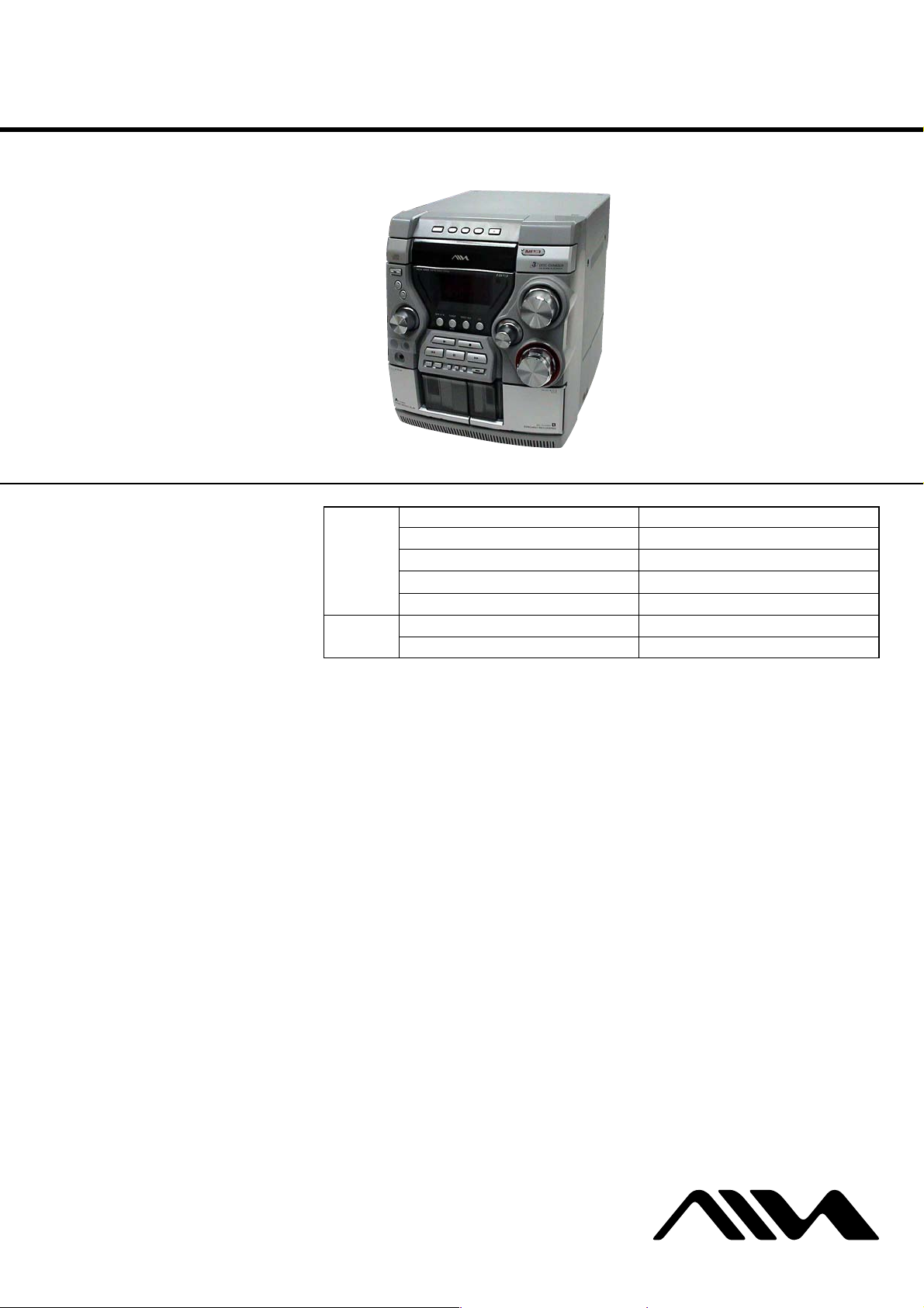
JAX-E3
SERVICE MANUAL
Ver 1.0 2003.06
•JAX-E3 is composed of the following models.
As service manuals are issued for each component model, please refer to them.
COMPONENT MODEL NAME
JAX-E3
COMPACT DISC DECK RECEIVER CX-JE3
SPEAKER SYSTEM SX-JE3
SPECIFICATIONS
Power requirements 230 V AC, 50/60 Hz
Power consumption 60 W
Power consumption With ECO mode on: 0.25 W
in standby mode With ECO mode off: 15 W
Dimensions (W x H x D) 280 x 330 x 392.5 mm
Weight
6.5 kg
ACCESSORIES
Part No. Description Remark
1-477-842-11 COMMANDER, STANDARD (RM-Z20004)
1-501-374-92 ANTENNA, LOOP (AM)
1-793-184-21 CONNECTOR (F TYPE ADAPTOR)
4-245-998-01 COVER, BATTERY (for RM-Z20004)
AEP Model
Supplied accessories
Remote commander (1)
Batteries (2)
FM antenna (1)
AM antenna (1)
Specifications and external appearance are subject to change
without notice.
4-246-024-12 MANUAL, INSTRUCTION
(ENGLISH, SPANISH, FRENCH, GERMAN, ITALIAN,
RUSSIAN, CZECH, HUNGARIAN, POLISH)
9-961-003-01 Sony Corporation
2003F05-1 Home Audio Company
C 2003.06 Published by Sony Engineering Corporation
MINI Hi-Fi COMPONENT SYSTEM
Page 2

JAX-E3
REVISION HISTORY
Clicking the version allows you to jump to the revised page.
Also, clicking the version at the upper right on the revised page allows you to jump to the next revised
page.
Ver. Date Description of Revision
1.0 2003.06 New
2
Page 3
CX-JE3
SERVICE MANUAL
Ver. 1.2 2005.05
CX-JE3 is the amplifier, CD player, tape deck
and tuner section in JAX-E3.
Model Name Using Similar Mechanism CX-JS3
CD
Section
Tape deck
Section
CD Mechanism Type CDM74S-K6BD71A
Base Unit Name BU-K6BD71A
Optical Pick-up Block Name KSM-213DCP
Optical Pick-up Name KSS-213D
Model Name Using Similar Mechanism CX-JS3
Tape Transport Mechanism T ype CWM43FF13
AEP Model
SPECIFICATIONS
TUNER
FM tuning range 87.5 MHz to 108 MHz
FM usable sensitivity (IHF) 16.8 dBf
FM antenna terminal 75 ohms (unbalanced)
AM tuning range 531 kHz to 1602 kHz
AM usable sensitivity 350 µV/m
AM antenna Loop antenna
AMPLIFIER
Power output
Total harmonic distortion 0.08 % (16 W, 1 kHz, 6 ohms, DIN
Input VIDEO/AUX: 400 mV
Outputs SPEAKER: 6 ohms or more
CASSETTE DECK
Track format 4 tracks, 2 channels stereo
Frequency response 50 Hz – 8 kHz
Recording system AC bias
Heads Deck A: playback x 1
Rated: 20 W + 20 W (6 ohms, T .H.D.
1 %, 1 kHz/DIN 45500)
Reference: 25 W + 25 W (6 ohms,
T.H.D. 10 %, 1 kHz/DIN 45324)
MUSIC POWER: 50 W + 50 W
AUDIO)
PHONES: 32 ohms or more
Deck B: recording/playback x 1,
erase x 1
CD PLAYER
Laser Semiconductor laser (λ = 780 nm)
D/A converter 1 bit dual
Signal-to-noise ratio 85 dB (1 kHz, 0 dB)
Harmonic distortion 0.05 % (1 kHz, 0 dB)
GENERAL
Power requirements 230 V AC, 50/60 Hz
Power consumption
Power consumption With ECO mode on: 0.25 W
in standby mode With ECO mode off: 15 W
Dimensions (W x H x D) 280 x 330 x 392.5 mm
Weight
Specifications and external appearance are subject to change
without notice.
COPYRIGHT
Check copyright laws relevant to recordings from discs, tuner
or tape for the country where the unit is to be used.
Licensed by BBE Sound, Inc. under USP4638258, 5510752
and 5736897.
Emission duration:
continuous
60 W
6.5 kg
9-961-005-03 Sony Corporation
2005E05-1 Personal Audio Group
© 2005.05 Published by Sony Engineering Corporation
COMPACT DISC DECK RECEIVER
Page 4
CX-JE3
Notes on chip component replacement
•Never reuse a disconnected chip component.
• Notice that the minus side of a tantalum capacitor may be damaged by heat.
Flexible Circuit Board Repairing
•Keep the temperature of the soldering iron around 270 ˚C during repairing.
• Do not touch the soldering iron on the same conductor of the
circuit board (within 3 times).
• Be careful not to apply force on the conductor when soldering
or unsoldering.
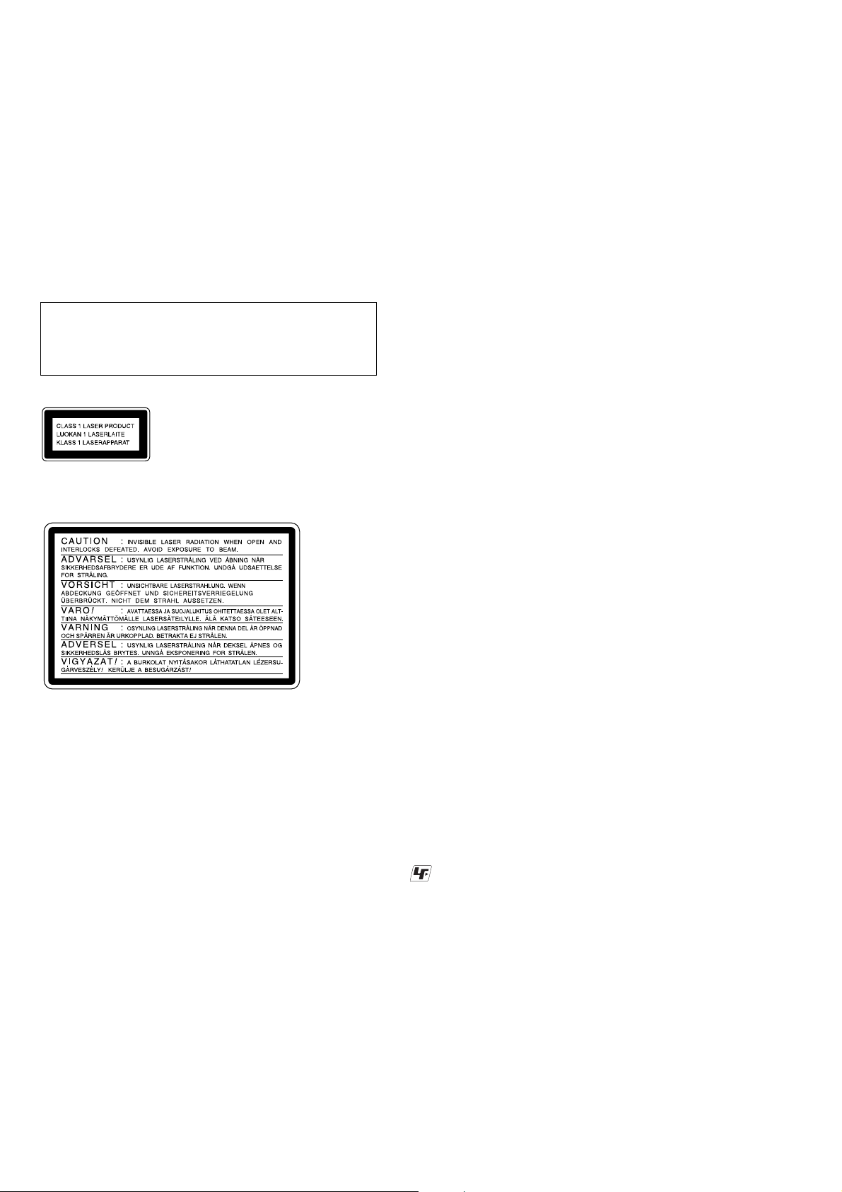
CAUTION
Use of controls or adjustments or performance of procedures
other than those specified herein may result in hazardous radiation exposure.
This appliance is classified as
a CLASS 1 LASER product.
The CLASS 1 LASER
PRODUCT MARKING is
located on the rear exterior.
The following caution label is located inside the unit.
SAFETY-RELATED COMPONENT WARNING!!
COMPONENTS IDENTIFIED BY MARK 0 OR DOTTED
LINE WITH MARK 0 ON THE SCHEMATIC DIAGRAMS
AND IN THE PARTS LIST ARE CRITICAL TO SAFE
OPERATION. REPLACE THESE COMPONENTS WITH
SONY PARTS WHOSE PART NUMBERS APPEAR AS
SHOWN IN THIS MANUAL OR IN SUPPLEMENTS PUBLISHED BY SONY.
UNLEADED SOLDER
Boards requiring use of unleaded solder are printed with the leadfree mark (LF) indicating the solder contains no lead.
(Caution: Some printed circuit boards may not come printed with
the lead free mark due to their particular size)
: LEAD FREE MARK
Unleaded solder has the following characteristics.
• Unleaded solder melts at a temperature about 40 ˚C higher than
ordinary solder.
Ordinary soldering irons can be used but the iron tip has to be
applied to the solder joint for a slightly longer time.
Soldering irons using a temperature regulator should be set to
about 350 ˚C.
Caution: The printed pattern (copper foil) may peel away if the
heated tip is applied for too long, so be careful!
• Strong viscosity
Unleaded solder is more viscou-s (sticky, less prone to flow)
than ordinary solder so use caution not to let solder bridges occur such as on IC pins, etc.
• Usable with ordinary solder
It is best to use only unleaded solder but unleaded solder may
also be added to ordinary solder.
2
Page 5

TABLE OF CONTENTS
CX-JE3
1. SERVICING NOTES ................................................ 4
2. GENERAL
Location of Controls ....................................................... 6
3. DISASSEMBLY
3-1. Disassembly Flow ........................................................... 8
3-2. Case (SIDE-L/R)............................................................. 9
3-3. Case (Top) ....................................................................... 9
3-4. Tray Panel........................................................................ 10
3-5. CD Mechanism Deck (CDM74S-K6BD71A)................ 10
3-6. Front Panel Section ......................................................... 11
3-7. Mechanical Deck (CWM43FF13) .................................. 11
3-8. Rear Cabinet Section ...................................................... 12
3-9. PT Board, MAIN Board.................................................. 12
3-10. Table Assy ....................................................................... 13
3-11. MOTOR (TB) Board....................................................... 13
3-12. MOTOR (LD) Board....................................................... 14
3-13. Base Unit (BU-K6BD71A)............................................. 14
3-14. Motor Gear Assy (Sled) (M701), BD Board .................. 15
4. TEST MODE.............................................................. 16
5. ELECTRICAL ADJUSTMENTS
CD Section ...................................................................... 17
6. DIAGRAMS
6-1. Block Diagram – CD Section – ..................................... 18
6-2. Block Diagram – TUNER/TAPE/PANEL Section –..... 19
6-3. Block Diagram – AMP/POWER SUPPLY Section – ... 20
6-4. Note for Printed Wiring Boards and
Schematic Diagrams ....................................................... 21
6-5. Printed Wiring Board – BD Section – ........................... 22
6-6. Schematic Diagram – BD Section – .............................. 23
6-7. Printed Wiring Boards – CHANGER Section –............ 24
6-8. Schematic Diagram – CHANGER Section – ................ 25
6-9. Schematic Diagram – MAIN Section (1/4) –................ 26
6-10. Schematic Diagram – MAIN Section (2/4) – ................ 27
6-11. Schematic Diagram – MAIN Section (3/4) – ................ 28
6-12. Schematic Diagram – MAIN Section (4/4) – ................ 29
6-13. Printed Wiring Board – MAIN Section – ...................... 30
6-14. Printed Wiring Board – HP Section – ........................... 31
6-15. Schematic Diagram – HP Section – .............................. 31
6-16. Printed Wiring Board – PANEL Section – .................... 32
6-17. Schematic Diagram – PANEL Section –....................... 33
6-18. Printed Wiring Boards – KEY Section – ....................... 34
6-19. Schematic Diagram – KEY Section – ........................... 35
6-20. Printed Wiring Board – PT Section – ............................ 36
6-21. Schematic Diagram – PT Section – ............................... 37
6-22. IC Pin Function Description ........................................... 41
7. EXPLODED VIEWS
7-1. Case Section .................................................................... 43
7-2. Front Panel Section-1...................................................... 44
7-3. Front Panel Section-2...................................................... 45
7-4. Front Panel Section-3...................................................... 46
7-5. Front Panel Section-4...................................................... 47
7-6. Chassis Section ............................................................... 48
7-7. CD Mechanism Deck Section-1
(CDM74S-K6BD71A) .................................................... 49
7-8. CD Mechanism Deck Section-2
(CDM74S-K6BD71A) .................................................... 50
7-9. CD Mechanism Deck Section-3
(CDM74S-K6BD71A) .................................................... 51
7-10. Base Unit Section (BU-K6BD71A) ............................... 52
8. ELECTRICAL PARTS LIST ............................... 53
3
Page 6
CX-JE3
SECTION 1
SERVICING NOTES
NOTES ON HANDLING THE OPTICAL PICK-UP
BLOCK OR BASE UNIT
The laser diode in the optical pick-up block may suffer electrostatic break-down because of the potential difference generated
by the charged electrostatic load, etc. on clothing and the human
body.
During repair, pay attention to electrostatic break-down and also
use the procedure in the printed matter which is included in the
repair parts.
The flexible board is easily damaged and should be handled with
care.
NOTES ON LASER DIODE EMISSION CHECK
The laser beam on this model is concentrated so as to be focused
on the disc reflective surface by the objective lens in the optical
pick-up block. Therefore, when checking the laser diode emission, observe from more than 30 cm away from the objectiv e lens.
LASER DIODE AND FOCUS SEARCH OPERATION
CHECK
Carry out the “S curve check” in “CD section adjustment” and
check that the S curve waveforms is output three times.
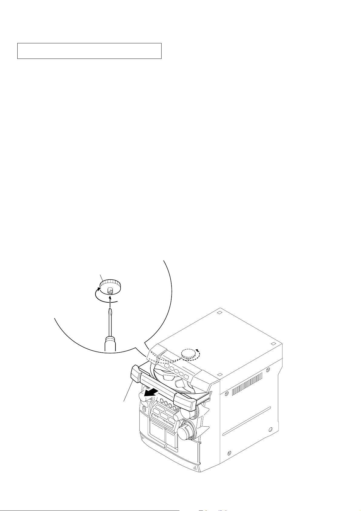
HOW TO OPEN THE DISC TRAY WHEN POWER SWITCH TURNS OFF.
1
Remove the case (side-L).
2
Turn the loading gear in the direction of arrow A.
A
3
Pull-out the disc tray.
4
Page 7
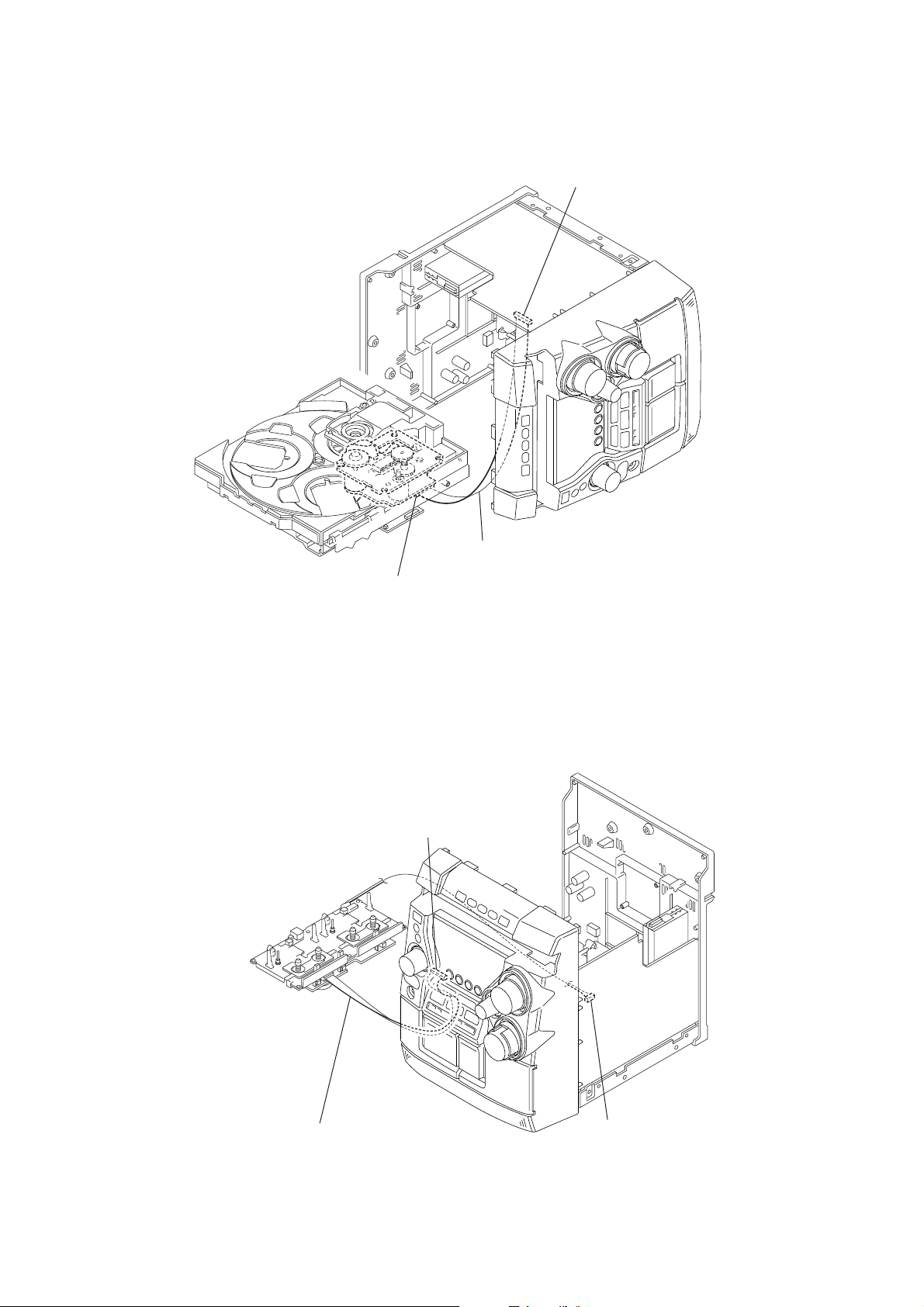
SERVICE POSITION
– CD mechanism deck –
CX-JE3
main board (CN691)
– Tape mechanism deck –
Connect wire (flat type) (19 core) to
main board (CN691) and BD board (CN710).
BD board (CN710)
panel board (CN601)
Connect wire (flat type) (13 core) to
panel board (CN601) and mechanical deck.
main board (CN301)
5
Page 8
CX-JE3
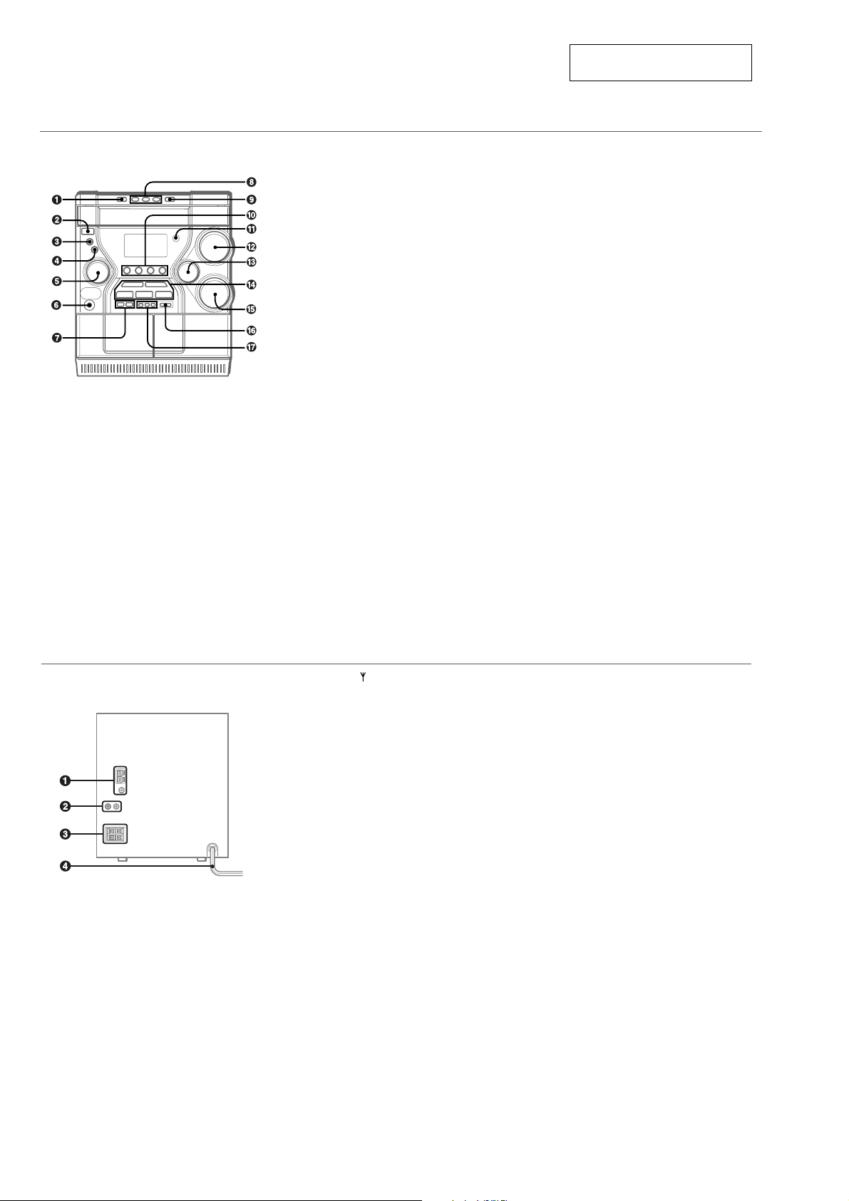
1 DISC CHANGE
Rotates the CD trays.
2 POWER 6STANDBY/ON
Switches the unit on and off (standby).
The red indicator flashes when receiving a signal from
the remote.
3 MODE
Selects various modes (ECO and Repeat/Shuffle/
Programmed playback, etc.) when used in combination
with ENTER and MULTI JOG.
4 ENTER
Fixes the modes and the time (ECO, Repeat/Shuffle/
Programmed playback, clock, and timer, etc.) when used
in combination with ENTER and MULTI JOG.
Main unit: front
5 MULTI JOG
When used in combination with ENTER and MULTI JOG,
CD: selects a track and Repeat/Shuffle/Programmed
playback.
Tuner: selects a preset station.
Tape: specifies tape length.
Clock and Timer: sets the time.
i-Bass: selects a frequency range.
Spectrum analyzer, ECO and Dimmer: selects the mode.
6 PHONES jack
Plug in here an optional headphones set with a mini
stereo plug (ø3.5 mm). Speaker output is canceled.
7 SYNC DUB
Starts dubbing a whole tape.
wREC/REC MUTING
Starts recording.
8 DISC DIRECT PLAY1-3
Selects a disc.
9 zOPEN/CLOSE
Opens or closes the disc compartment.
0 TAPE A/B
Selects Tape function, and deck A or B.
TUNER/BAND
Selects Tuner function and the radio band.
VIDEO/AUX
Selects the function of external equipment connected to
VIDEO/AUX jacks.
CD
Selects CD function.
! Remote sensor
Receives a signal from the remote.
@ VOLUME
Adjusts the volume.
CD: searches a track in fast forward or fast reverse
playback when held down.
Tape: fast forwards or rewinds the tape.
Tuner: manually tunes down or up within the band.
aPAUSE/SET
CD and Tape: pauses playback.
Tuner: stores the received station in to preset.
% BASS
Emphasizes low frequency sound.
^ i-Bass
Produces rich and clear low frequency sound.
& DISPLAY
Displays the time and the remaining time for CD.
ALBUM k, i
Selects a previous album or a succeeding album with
MP3-CDs.
PTY
Displays a program type for RDS (Radio Data System)
• LOCATION OF CONTROLS
SECTION 2
GENERAL
This section is extracted from
instruction manual.
# TREBLE
Enhances high frequency sound.
$ cPLAY/PRESET
When the unit is turned off: activates or deactivates
DEMO.
CD and Tape: starts playback.
Tuner: tunes into a preset station.
sSTOP/CLEAR
CD and Tape: stops playback.
Tuner: clears a station preset.
fTUNING DOWN, gTUNING UP
Main unit: rear
6
1 AM LOOP, FM 75Ω terminals
Plug in the supplied AM and FM antennas here.
2 VIDEO/AUX jacks
Accepts analog sound signals from external equipment.
Connect using an optional connecting cable with RCA
phono plugs (red plug to R jack, white plug to L jack).
Refer also to the operating instructions of your equipment.
To switch function to external input, press VIDEO/AUX.
Tip:
To change the displayed name for this function, turn the
unit on, then hold down VIDEO/AUX and press POWER
on the unit. Repeat the procedure to select "VIDEO",
"AUX" or "TV".
3 # SPEAKER terminals
Connect the speaker cord of the supplied front speakers
here.
4 AC power cord
Page 9
CX-JE3
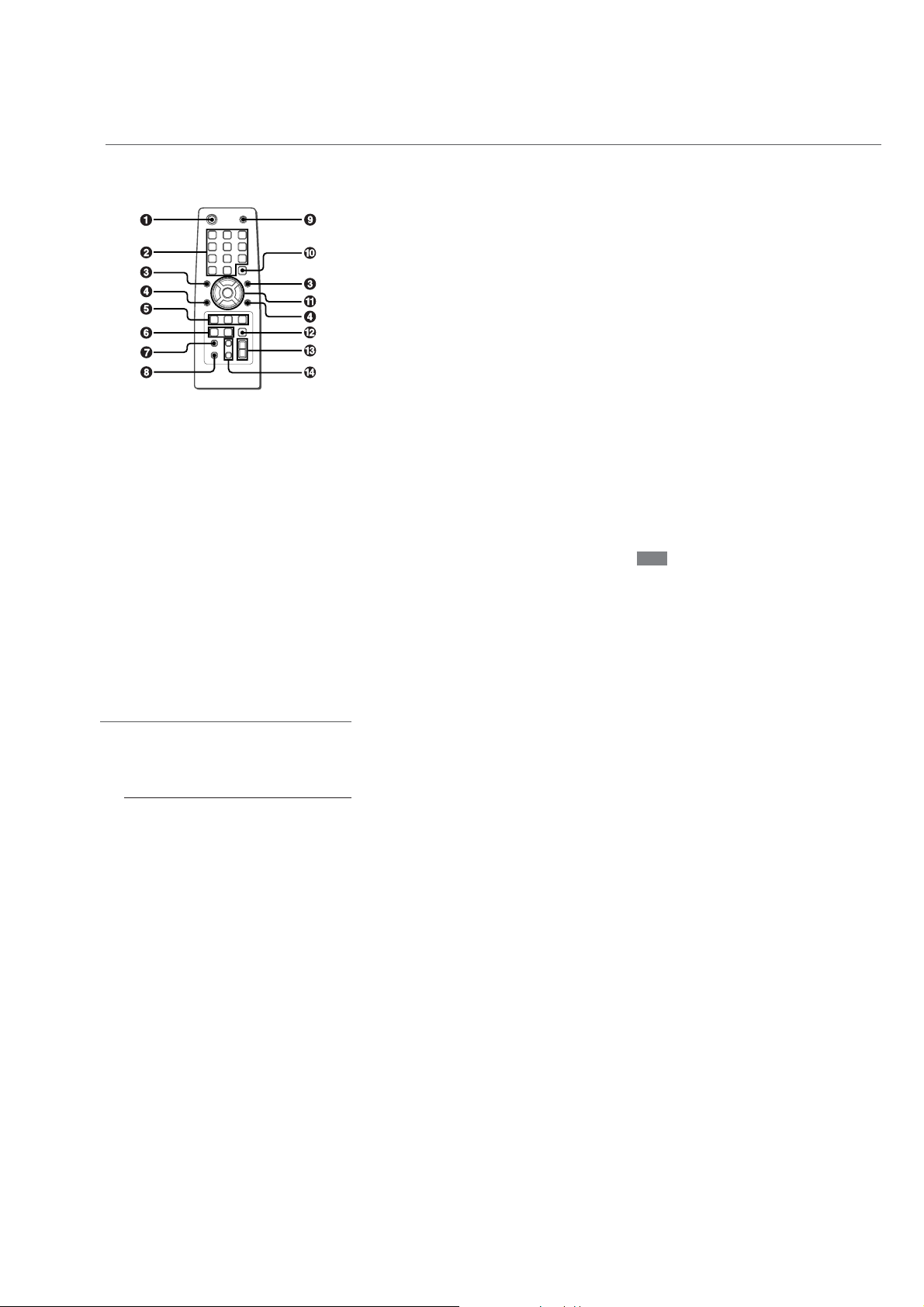
Remote control
Buttons with the same or similar names with the main unit
basically have the same function.
1 POWER
2 1-0/10, +10
CD: selects a CD track of the specified number.
Tuner: tunes in to the station with the specified preset
number.
The numbered buttons take on these functions below when pressed
with SHIFT held down
EDIT
Enters AI Edit Recording or Programmed Edit Recording
mode when pressed in stop mode.
BAND
Selects Tuner function and the radio band.
TAPE A/B
:
SPECTRUM
Changes the spectrum analyzer display.
TUNER MODE
Switches between stereo or monaural FM reception.
3 r, t
CD: selects a track.
Tuner: selects a preset station.
Tape: specifies tape length.
BASS and TREBLE: adjusts the level.
Clock and Timer: sets the time.
4 ALBUM M, N
Selects a previous album or a succeeding album.
5 PLAY MODE
Selects Shuffle or Programmed playback in CD function.
REPEAT
Enters CD repeat playback mode.
ENTER
6 CLOCK/TIMER/SET
Enters timer setting mode.
CLOCK/TIMER/SELECT
Selects timer playback, timer recording or timer off.
7 DISPLAY
8 SHIFT
Hold down when pressing a numbered button to change
its function to that printed above the number.
e.g.)
"Press SHIFT+BAND on the remote" indicates "Hold
down SHIFT and press '2' (BAND)". Doing so makes you
be able to select Tuner function and the radio band.
9 FUNCTION
Switches the active function among CD, TAPE, TUNER
and VIDEO (AUX or TV).
0 DISC SKIP
Select a disc.
! c/d
When the unit is turned off: activates or deactivates
DEMO.
CD and Tape: starts playback.
s
CD and Tape: stops playback.
f,g
CD: searches a track in fast forward or fast reverse
playback when held down.
Tape: fast forwards or rewinds the tape.
Tuner: manually tunes down or up within the band.
a
CD and Tape: pauses playback.
@ SLEEP
Switches the sleep-timer on/off and selects the duration.
# VOLUME (+, -)
Adjusts the volume.
$ SOUND
Selects BASS or TREBLE setting mode
CLEAR
Clears a track of the CD programmed playback and a
Radio preset station.
Note
The button not explained above (KARAOKE) does not
operate for this unit.
Setting the clock
Use the remote.
1
Press CLOCK/TIMER/SET.
Go to step 3 when the time appears and the 'hour' flashes.
2
Press r or t repeatedly until "CLOCK
SET" appears in the display and then press
ENTER.
3
Press r or t repeatedly to set the hour
and then press ENTER.
4
Press r or t repeatedly to set the minute
and then press ENTER.
The time display stops flashing and the clock starts from
00 seconds.
•MULTI JOG is also available in place of r or t.
To display the time
Press DISPLAY on the remote. The time will be displayed for
6 seconds.
If "- -:- -" appears when the unit is turned off
There has been a power interruption. Re-set the clock.
7
7
Page 10
CX-JE3
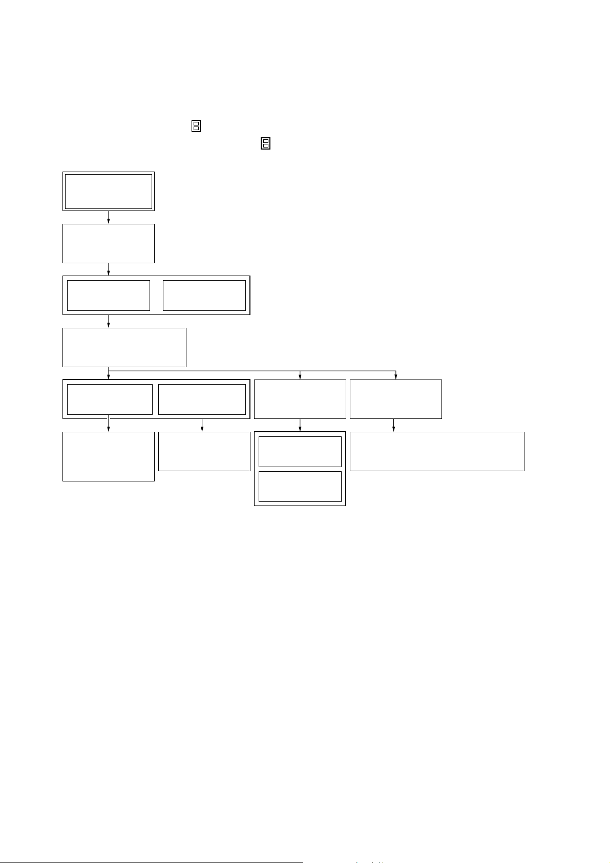
• This set can be disassembled in the order shown below.
3-1. DISASSEMBLY FLOW
Note 1: The process described in can be performed in any order.
Note 2: Without completing the process described in , the next process can not be performed.
Set
3-2. CASE
(SIDE-L/R)
(Page 9)
SECTION 3
DISASSEMBLY
3-3. CASE (TOP)
(Page 9)
3-5. CD MECHANISM DECK
(CDM74S-K6BD71A)
(Page 10)
3-6. FRONT PANEL
SECTION
(Page 11)
3-7. MECHANICAL
DECK
(CWM43FF13)
(Page 11)
3-4. TRAY PANEL
3-8. REAR CABINET
3-9. PT BOARD,
(Page 10)
SECTION
(Page 12)
MAIN BOARD
(Page 12)
3-10. TABLE ASSY
(Page 13)
3-11. MOTOR (TB)
BOARD
(Page 13)
3-12. MOTOR (LD)
BOARD
(Page 14)
3-13. BASE UNIT
(BU-K6BD71A)
(Page 14)
3-14. MOTOR GEAR ASSY (SLED) (M701),
BD BOARD
(Page 15)
8
Page 11
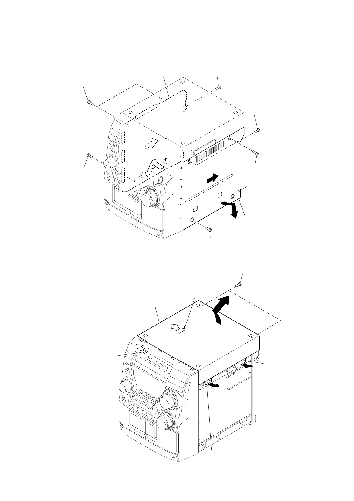
Note: Follow the disassembly procedure in the numerical order given.
s
w
3-2. CASE (SIDE-L/R)
5
case (side-L)
1
two case screws
3
2
two screws
(BVTP3
×
10)
2
two screws
(BVTP3
×
CX-JE3
10)
1
case screw
3-3. CASE (TOP)
4
case (top)
4
2
claw
3
1
3
4
case screw
1
5
case (side-R)
1
two screws
(BVTP3 × 10)
two case screw
2
claw
2
cla
2
claw
9
Page 12
CX-JE3
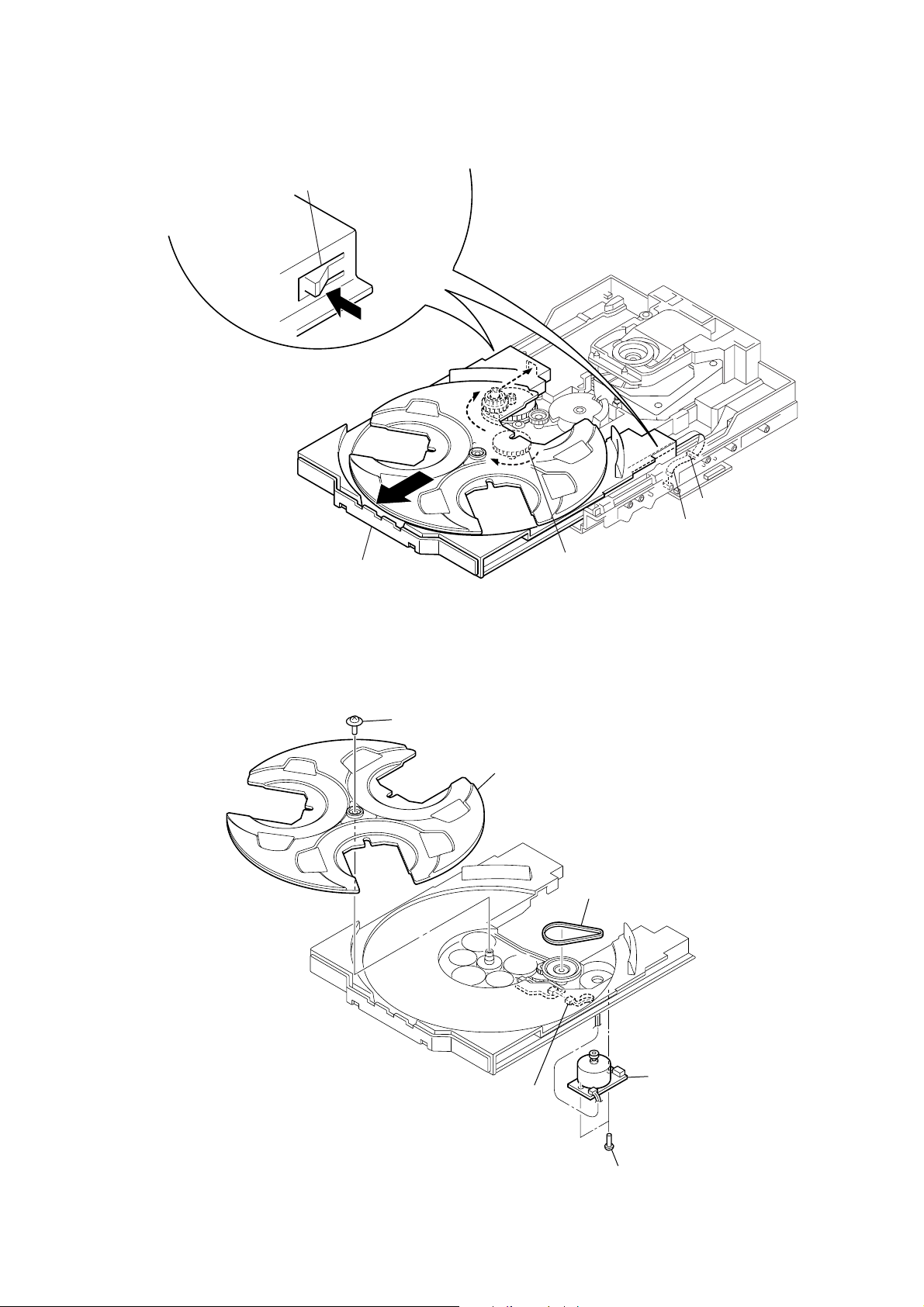
3-4. TRAY PANEL
1
Turn the loading gear
in the direction of arrow
2
Pull-out the disc table.
A
four claws
3
.
A
4
tray panel
3-5. CD MECHANISM DECK (CDM74S-K6BD71A)
5
CD mechanism deck
(CDM74S-K6BD71A)
3
screw
(BVTP3
×
10)
1
wire (flat type) (19 core)
(CN691)
2
connector
(CN701)
4
two screws
(BVTP3
×
10)
10
3
screw
(BVTP3
×
10)
Page 13
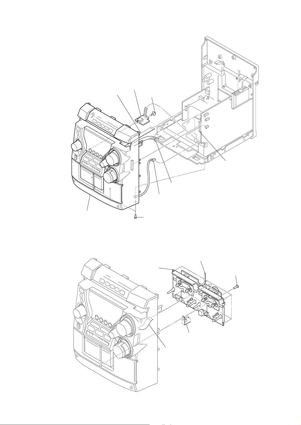
3-6. FRONT PANEL SECTION
3
wire (flat type) (11 core)
(CN694)
2
headphone board
1
CX-JE3
screw
(BVWHTP)
7
front panel section
3-7. MECHANICAL DECK (CWM43FF13)
4
5
three screws
(BVTP3 × 10)
mechanical deck
(CWM43FF13)
4
connector
(CN301)
4
connector
(CN302)
3
clamp
2
six screws
(BVTP3
6
connector
(CN101)
×
10)
5
ground mechanical plate
1
wire (flat type) (13 core)
11
Page 14
CX-JE3
3-8. REAR CABINET SECTION
1
wire (flat type) (15 core) (CN802)
3
rear cabinet section
2
2
three screws
(BVTP3
screw
(BVTP3
×
×
10)
10)
3-9. PT BOARD, MAIN BOARD
3
screw
5
two screws
(ITC4
6
PT board
(BVTP3
×
10)
5
two screws
×
8)
(ITC4
2
screw
×
8)
(BVTT3 × 8)
1
connector (CN091)
4
Remove the PWB PT HLDR
in the direction of the arrow.
8
main board
7
screw
(BVTT3 × 8)
12
7
two screws
(BVTT3 × 8)
Page 15
3-10. TABLE ASSY
)
d
two claws
5
CX-JE3
Ver. 1.2
A
2
Pull-out the table assy.
6
table assy
3-11. MOTOR (TB) BOARD
1
screw
(PTPWH M2.6)
2
tray
1
Turn the loading gear
in the direction of arrow
3
belt (table)
4
hook
3
wire (flat type) (5 core
(CN702)
A
.
4
connector
(CN731)
6
motor (TB) boar
5
two screws
(BTTP M2.6)
13
Page 16
CX-JE3
3-12. MOTOR (LD) BOARD
4
motor (LD) board
3
two screws
(BTTP M2.6)
1
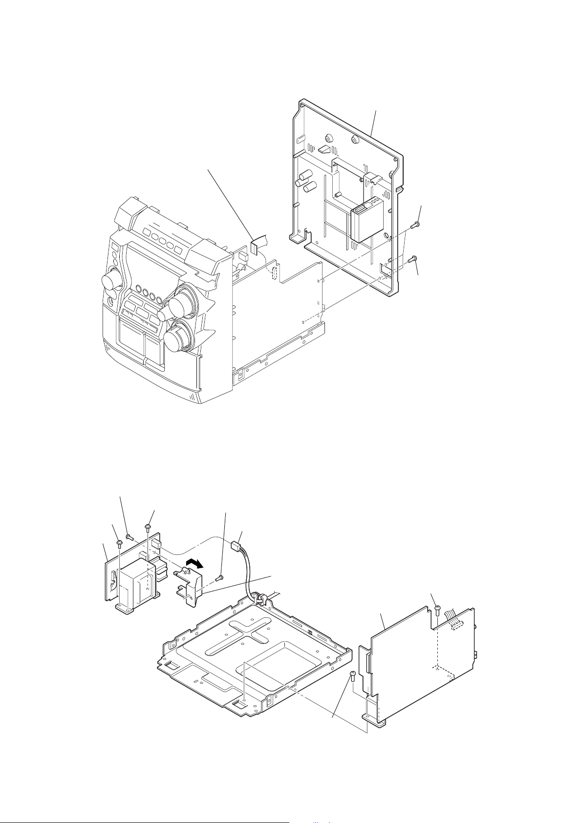
3-13. BASE UNIT (BU-K6BD71A)
belt (loading)
2
connector
(CN704)
8
base unit
(BU-K6BD71A)
14
4
three insulators
3
three coil springs
(insulator)
2
three stoppers (BU)
1
threescrews
(BTTP M2.6)
7
insulator
6
coil spring
(insulator)
5
screw
(PTPWH M2.6)
Page 17
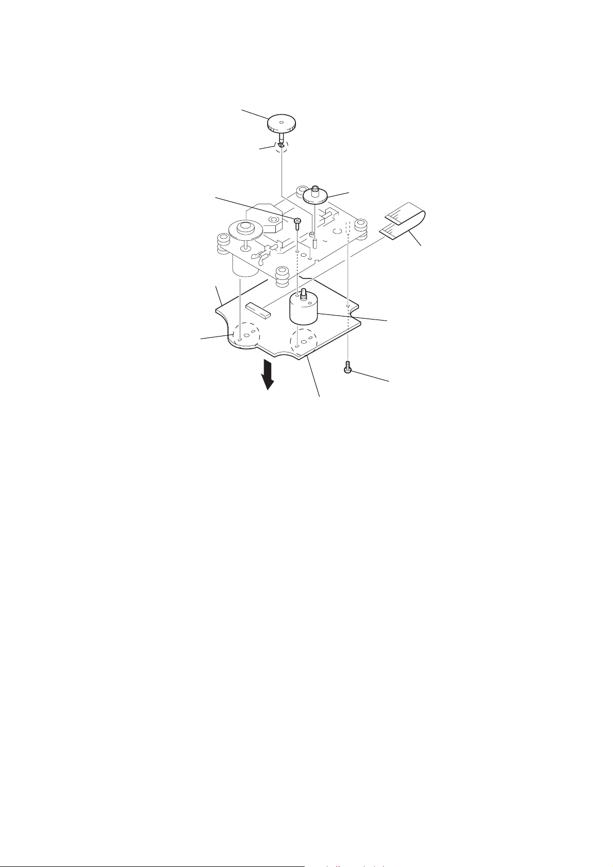
)
3-14. MOTOR GEAR ASSY (SLED) (M701), BD BOARD
7
gear (A)
6
claw
2
two screws
×
3)
(P2
qa
BD board
1
Remove two
solders.
8
gear (B)
5
wire (flat type) (16 core
(CN708)
0
motor gear assy (SLED)
(M701)
CX-JE3
4
9
Remove two solders.
3
screw (P2.6 × 6)
15
Page 18

CX-JE3
SECTION 4
TEST MODE
MC COLD RESET
• The cold reset clears all data including preset data stored in the
RAM to initial conditions. Execute this mode when returning
the set to the customer.
Procedure:
1. In the standby status, while pressing the x button, press the
[POWER] button.
2. The set is reset, then becomes standby status.
GC TEST MODE
Procedure:
1. Press the [POWER] button to turn the power on.
2. While pressing the x button, press the [POWER] button for
5 seconds.
3. It change displays in order of model type, version and suffix at
2 seconds interval, then the display is back to normal status.
AMP TEST MODE
Procedure:
1. In the status where AC plug is disconnected, while pressing
the [VIDEO/AUX] button, connect the AC plug to turn the
power on. Then enter the AMP test mode and display “AMP
TEST”.
2. If turn the [VOLUME] knob clockwise, it displays “VOLUME
MAX”, and if turn the knob counterclockwise, it displays
“VOLUME 0”.
3. If the [TREBLE] and [BASS] knobs are turned clockwise or
counterclockwise, it change displays in order of “EQ MAX”,
“EQ MIN” and “EQ FLAT”.
4. To release from this mode, disconnect the AC plug and turn
the power off.
FUNCTION CHANGE MODE
• Select either TV, VIDEO or AUX (MD) of the external function
input.
Procedure:
1. Press the [POWER] button to turn the power on.
2. While pressing the [VIDEO/AUX] button, press the [POWER]
button.
3. Each time this operation is operated, it change displays in or-
der of “TV”, “VIDEO” and “AUX”.
DISC TRAY LOCK
Procedure:
1. Press the
2. While pressing the x button, press the [ OPEN/CLOSE]
button for 5 seconds.
3. The message “LOCKED” is displayed and the tray is locked.
(Even if exiting from this mode, the tray is still locked)
4. To release this lock, while pressing the x button, press the
[ OPEN/CLOSE] button for 5 again.
Z
5. The message “UNLOCKED” is displayed and the tray is unlocked.
CD REPEAT 5 LIMIT CANCEL MODE
• Number of repeat for CD playback is 5 times when the repeat
mode is “REPEAT”. This mode enables CD to repeat playback
for limitless times.
Procedure:
1. Press the [POWER] button to turn the power on.
2. In the repeat on status, while pressing the x button, press the
[POWER] button to turn the power on.
Z
[CD] button to enter the CD repeat 5 limit cancel mode and
repeat mark blinks on the fluorescent indicator tube.
3. To release this mode, press the [POWER] button to turn the
power off.
16
Page 19
SECTION 5
BD board
Oscilloscope
TP(FE)
TP(VC)
symmetry
S-curve waveform
within 3
±
0.5Vp-p
A
B
p
ELECTRICAL ADJUSTMENTS
CX-JE3
CD TEST MODE
•This mode can run the CD sled motor freely. Use this mode, for
instance, when cleaning the pickup.
Procedure:
1. In the status where AC plug is disconnected, while pressing
the [CD] button, connect the AC plug to turn the power on.
2. When enter this mode, it displays “CD TEST” and few sec-
onds later, all segments turn on of the fluorescent indicator
tube.
3. To release from this mode, disconnect the AC plug and turn
the power off.
In this mode, it operates as following table.
Button Operation Purpose of use
M Move the pick-up to outside track Sled circuit check
m Move the pick-up to inside track Tracking circuit check
Mechanism operation check
Optical pick-up check
N Playback a CD Servo block check
If it cannot focus on, it continuous focus search
x When playback a CD: stop playback APC circuit check
When stop a CD: Laser current measure
display “READING” (blink) Focus search waveform check
continuous laser diode on Tracking balance check
continuous focus search (not made focus on)
X Pause, Tracking servo off
(ignore CLV error)
CD SECTION
Note:
1. CD Block is basically designed to operate without adjustment. Therefore,
check each item in order given.
2. Use YEDS-18 (3-702-101-01) unless otherwise indicated.
3. Use an oscilloscope with more than 10MΩ impedance.
4. Clean the object lens by an applicator with neutral detergent when the
signal level is low than specified value with the following checks.
S-CURVE CHECK
Procedure :
1. Connect an oscilloscope to TP (FE) and TP (VC).
2. Turn the power on.
3. Load a disc (YEDS-18) and actuate the focus search. (In
consequence of open and close the disc tray, actuate the focus
search)
4. Confirm that the oscilloscope waveform (S-curve) is
symmetrical between A and B. And confirm peak to peak level
within 3 ± 0.5 Vp-p.
Note: Clear RF signal wav eform means that the shape “ ◊ ” can be clearly
distinguished at the center of the waveform.
RF signal waveform
VOLT/DIV : 200mV
TIME/DIV : 500ns
±
level : 1.3
0.3Vp-
Connecting Location: BD board
– BD Board (Conductor side) –
Note: •Try to measure several times to make sure than the ratio
of A : B or B : A is more than 10 : 7.
•Take sweep time as long as possible and light up the
brightness to obtain best waveform.
RF LEVEL CHECK
oscilloscope
BD board
TP(RF)
TP(VC)
Procedure :
1. Connect an oscilloscope to TP (RF) and TP (VC).
2. Turn the power on.
3. Load a disc (YEDS-18) and playback.
4. Confirm that oscilloscope waveform is clear and check if RF
signal level is correct or not.
TP (RF)
IC721
TP (VC)
TP (FE)
1717
Page 20
CX-JE3
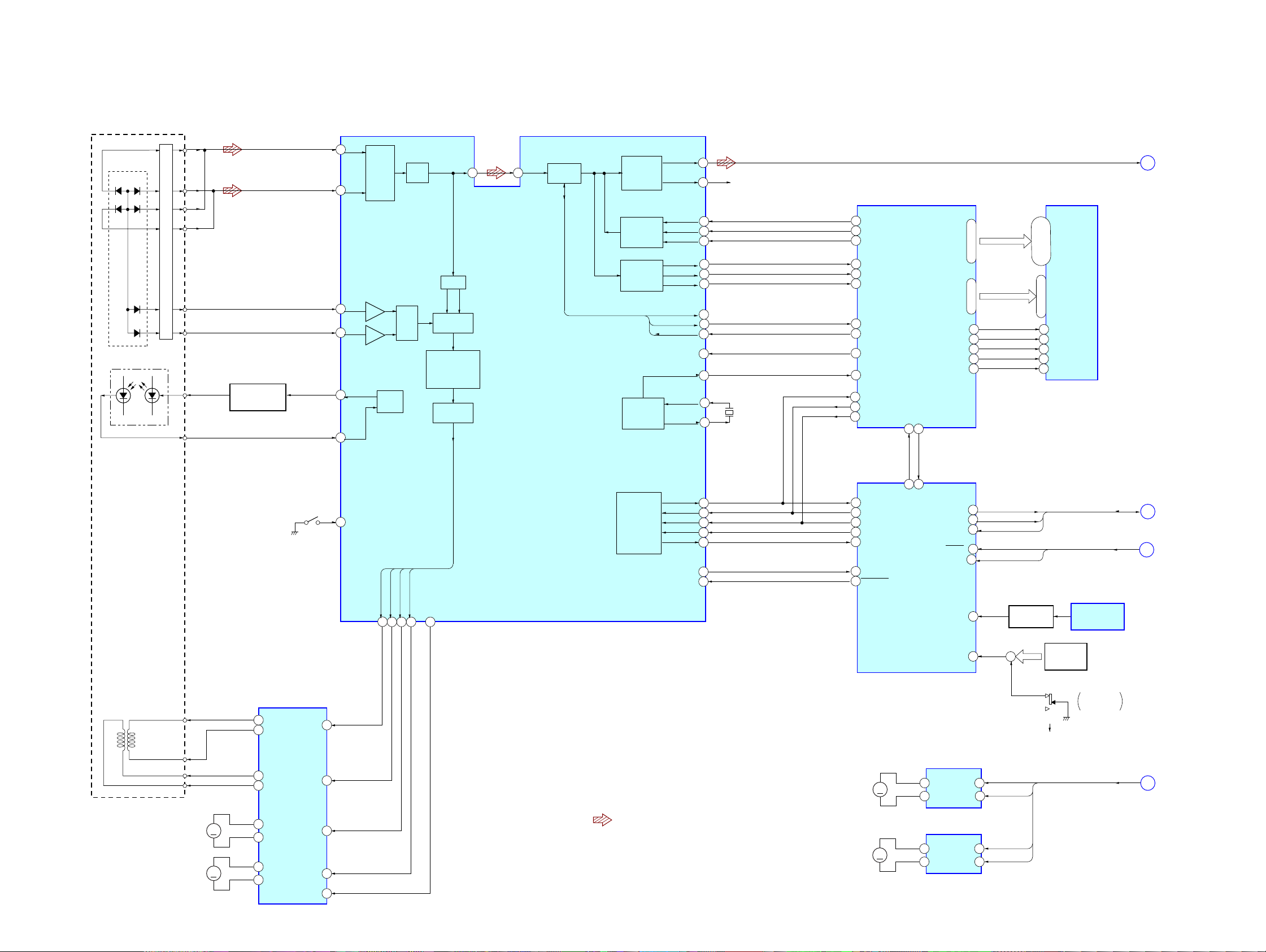
SECTION 6
DIAGRAMS
6-1. BLOCK DIAGRAM – CD Section –
OPTICAL PICK-UP
BLOCK
(KSM-213DCP)
A
DETECTOR
A
D
C
B
E
F
LASER DIODE
PD
D
C
I-V AMP
B
E
F
LD
LD
PD
AUTOMATIC
POWER CONTROL
Q701
8
7
9
10
80
79
CD DSP
IC721
FIN2
FIN1
TIN1
TIN2
LDD
LDS
RF AMP
APC
TBAL
EQ,
AGC
RF
PH, BH
A/D
CONVERTER
SERVO
PROCESSOR
D/A
CONVERTER
LCHO
EFMIN
4
3
ERROR
CORRECT
D/A
CONVERTER
EXTERNAL
AUDIO IN
SERIAL OUT
CLOCK
GENERATOR
FSX/16MIN
RCHO
ASDFIN
ASDACK
ASLRCK
DATA
DATACK
LRSY
EFLG
C2F
16MOUT
XIN
XOUT
42
45
57
56
55
60
59
58
53
52
50
26MP3RES
54
49
48
16.9344MHz
X701
R-CH
2 ADDATA
3 ADBCK
4 ADLRCK
79 DATAIN
80 DATACK
1 LRSY
5 C2FIN
9 CKOUT
78 RESB
7 CKIN
73 CMDOUT
74 CMDIN
75 CL
MP3 DECODER
IC801
CE
FSYNC
76
66
MDATA0
– MDATA15
23-30, 33-40
MADRS0
– MADRS8
60-53, 50
45OEB
42WEB
41RASB
43CASLB
44CASUB
IC802
MEMORY
2-5, 7-10,
35-38, 40-43
A0 – A8
18-21, 24-28
29 OE
15 WE
16 RAS
31 LCAS
30 UCAS
I/O1 – I/O16
CD
(Page 20)
A
2-AXIS
DEVICE
(FOCUS)
(TRACKING)
M701
(SLED)
M702
(SPINDLE)
10
6
DO
64
DI
63
WRQ
CL
62
CE
61
65
67DRF
66RES
S701
(LIMIT)
FOCUS/TRACKING COIL DRIVE,
SPINDLE/SLED MOTOR DRIVE
IC722
18
VO3(+)
17 VO3(–)
11 VO2(+)
12 VO2(–)
FOIN
20TIN
10
70 LIMIT SW
20
TDO
21
FDO
SLDO
23
SPDO
22
CONT4
25
COMMAND
INTERFACE
• R-ch is omitted due to same as L-ch.
• SIGNAL PATH
M
M
26 VO4(+)
27 VO4(–)
2 VO1(+)
1 VO1(–)
25SLIN
3SPIN
7LDS
: CD
99 CD DO
98 CD DI
100 C D CLK
5 CD CE
97 CD WRQ
95 CD DRF
4 CD RESET
M751
(LOADING)
M741
(TABLE)
MP3 CE
MP3 SYNC
SYSTEM CONTROLLER
IC901 (1/2)
LOADING MOTOR DRIVE
M
M
1MUTE
94POWER
27HOLD
11RESET
18POWER DOWN
74CD NUMBER SENS
20CD BUSY
IC701
4 OUT1
2 OUT2
TABLE MOTOR DRIVE
IC712
4 OUT1
2 OUT2
MUTE
POWER
HOLD
RESET
P-DOWN
OPEN
ROTARY
ENCODER
S711
TABLE ADDRESS
LEVEL SHIFT
Q731
+
CLOSE
LM-F
7FIN
LM-R
9RIN
TM-F
7FIN
TM-R
9RIN
O-MUTE,
O-POWER,
SENSOR
IC731
S751
OPEN/CLOSE
DETECT
LM-L, LM-R,
TM-L, TM-R
HOLD
RESET,
P-DOWN
B
C
D
(Page 20)
(Page 20)
(Page 20)
1818
Page 21
6-2. BLOCK DIAGRAM – TUNER/TAPE/PANEL Section –
FM/AM TUNER PACK
FM 75Ω
(COAXIAL)
AM LOOP
FM ANT
AM ANT
L-CH
R-CH
TUNED
STEREO
MUTE
RDS DATA
RDS INT
FM-SOUT
R-CH
DO
DI
CL
CE
DATA
IFC
CLK
PLL-CE
TUNED
STEREO
TU-MUTE
RDS-DATA
RDS-CLK
RDS-SIG
TU
DATA
IFC
CLK
PLL-CE
TUNED
STEREO
TU-MUTE
RDS-DATA
RDS-CLK
RDS-SIG
E
(Page 20)
DATA
CLK
3 TU/EVOL DO
96 TU DI
88 CLK
9 TU CE
75 TUNED
76 STEREO
85 TU MUTE
2 RDS DO
28 RDS CKL
19 TU-SIG/MIC
SYSTEM CONTROLLER
IC901 (2/2)
LCK
XT1
CF1
CF2
CX-JE3
PB,
REC
B+
(CD-VM)
DATA, CLK,
S-OUT, LCK
TAPE MECHANISM
DECK BLOCK
MM
(CAPSTAN/REEL)
(DECK-A)
(DECK-B)
F
G
(Page 20)
(Page 20)
REC
Q310
MOTOR DRIVE
Q601, 604
(DECK-A)
Q602, 605
(DECK-B)
Q603, 606
PB
REC BIAS
SWITCH
Q311, 312
CAPM+
A-SOL
B-SOL
MUTING
Q305
MUTING
Q307, 309
PB SWITCH
Q301
PB SWITCH
Q303
18
SO
5 LCK
3 DATA
4 CLK
Q601
6
PB2
O-MOTOR
R-CH
O-BIAS
SOL A
SOL B
BIAS OSC
L311
7
8
9
10
BIAS OSC
CAPSTAN/REEL
PLUNGER DRIVE
PLUNGER DRIVE
L-CH
HP1
(PB)
(DECK-A)
HRPE1
(REC/PB/ERASE)
(DECK-B)
8
X901
32.768kHz
1312XT2
15
16
X902
8.64MHz
R-CH R-CH
L-CH
R-CH R-CH
ERASE
CLK
DATA
LCK
S-OUT
(Page 20)
H
SPEANA
• R-ch is omitted due to same as L-ch.
• SIGNAL PATH
: TUNER
: TAPE PLAY (DECK-A)
: TAPE PLAY (DECK-B)
: TAPE REC
SPEANA
AMP
Q201, 202
VOLUME
TREBLE
BASS
MULTI JOG
S301 – 323
(FRONT PANEL KEY)
BAND-PASS
FILTER
Q204 – 206
ROTARY
ENCODER
S801
ROTARY
ENCODER
S803
ROTARY
ENCODER
S802
ROTARY
ENCODER
S804
REMOTE CONTROL
RECEIVER
IC801
21 SPEANA-L
22 SPEANA-M
23 SPEANA-H
77 VOL A
78 VOL B
81 TRE A
82 TRE B
83 BASS A
84 BASS B
79 JOG A
80 JOG B
KEY1 –
KEY3
26 – 24
29 RMC
KEYSCAN
A PHOTO/S6
B PHOTO/S7
A HALF/S12
B HALF/S10
A MODE/S13
B MODE/S9
REC FWD/S11
REC REV/S8
S14 – S25
S1 – S5,
S26 – S30
G1 – G11
93POWER LED
92
47
48
54
52
55
50
53
49
41-45,
56-6730-40
68-71,73
S6
S7
S12
S10
S13
S9
S11
S8
LED901
1 STANDBY/ON
LED201
i-BASS
B+ SWITCH
Q607
B+
D620 – 627
S6 – S13
B+
FL901
FLUORESCENT
INDICATOR TUBE
11 V-BASS
MOTOR/PLUNGER DRIVE,
+3.3V
LED DRIVE
IC201
S6
S7
S12
S10
S13
S9
S11
S8
A-PHOTO
B-PHOTO
A-HALF
B-HALF
A-MODE
B-MODE
REC (FWD)
REC (REV)
1919
Page 22

CX-JE3
6-3. BLOCK DIAGRAM – AMP/POWER SUPPLY Section –
(Page 19)
(Page 18)
(Page 19)
(Page 19)
(Page 18)
SPEANA
H
J602
VIDEO/AUX
A
E
F
D
L
R
CD
TU
PB, REC PB
LM-L, LM-R,
TM-L, TM-R
R-CH
REC
CURRENT
Q101, 103
DETECT
Q281
MIRROR
Q105, 107
CASCADE
Q111
BIAS
Q117, 119
FINAL DRIVE
Q121, 123
R-CH
OVER LOAD
DETECT
Q129
+
HOLD
Q282
+
R-CH
+
+
DC DETECT
Q063, 064
HOLD
Q045, 046
+
TH101, 102
THERMAL DETECT
Q291, 292
PROTECT
Q047
R-CH
PHONES
J203
SPEAKER
+
–
+
–
J221
L
R
17
A-IN
19
B-IN
21
PB-OUT
C-IN
23
PB1P
2
REC1O
28
CONT
13
INPUT SELECT,
ELECTRICAL VOLUME
IC601
7
VOL-IN
LM-L
LM-R
TM-L
TM-R
BASS
OUT
BASS BOOST ENHANCER
1
18
INA
BOOST
CONTROL
Q674 – 677
8 – 11 5 – 7
BOOST1 –
BOOST4
LM-L
14
LM-R
15
TM-L
12
TM-R
13
IC671
OUTA6
GIN14VREF7BBE
13
BBE CONTROL,
LOADING/TABLE
MOTOR DRIVE
IC672
6
FREQUENCY
CONTROL
Q671 – 673
FREQ1 –
FREQ3
DATA3CLK
2
PRE DRIVE
MUTING
Q181
R-CH
MUTING
CONTROL
Q183
16
BBE
LCK
4
OVER CURRENT
(Page 19)
(Page 18)
G
C
DATA, CLK,
S-OUT, LCK
RESET,
P-DOWN
• R-ch is omitted due to same as L-ch.
• SIGNAL PATH
: CD
: TUNER
: TAPE PLAY (DECK-A)
: TAPE REC
: AUX IN
RESET
P-DOWN
RESET SWITCH
Q901
DATA
RESET SIGNAL
GENERATOR
IC502
+3.3V
D504
+4V
REGULATOR
IC501
V-STBY
+1.8V (MP3)
S-OUT
RECT
D091, 092
LCK
CLK
+1.8V
REGULATOR
IC803
+3.3V (CD)
+4V
POWER TRANSFORMER
(SUB)
PT011
VCC
MUTE
D697
+4V
REGULATOR
IC003
B+ SWITCH
Q023, 024
POWER
FLUORESCENT
INDICATOR TUBE
POWER
VDD
VM
CD-VM
POWER AMP
BLOCK
VF1
VF2
–VFL
D691 – 694
TO
VSS
+6.4V (CD)
TO
REGULATOR
REGULATOR
–VH
+VL
–VL
–27V
REGULATOR
Q041, 043
+9V
IC002
+9V
IC001
RECT
D019, 020
RECT
D041 – 044
RECT
D010
HOLD
RELAY DRIVE
POWER TRANSFORMER
(MAIN)
PT002
VL1
VL2
VH1
VH2
RY001
Q022
(AC IN)
MUTE, POWER,
HOLD
B
(Page 18)
2020
Page 23

CX-JE3
CD KEY board
SENSOR board
BD board
MOTOR (TB) board
DRIVER board
MOTOR (LD) board
SW board
KEY board
PT board
HEADPHONE board
PANEL board
MAIN board
TUNER PACK
6-4. NOTE FOR PRINTED WIRING BOARDS AND SCHEMATIC DIAGRAMS
Note on Printed Wiring Board:
• X : parts extracted from the component side.
• Y : parts extracted from the conductor side.
• : Pattern from the side which enables seeing.
(The other layers' patterns are not indicated.)
Caution:
Pattern face side: Parts on the pattern face side seen from
(Conductor Side) the pattern face are indicated.
Parts face side: Parts on the parts face side seen from
(Component Side) the parts face are indicated.
• Indication of transistor.
C
Q
B
E
B
These are omitted.
Q
CE
These are omitted.
Note on Schematic Diagram:
• All capacitors are in µF unless otherwise noted. pF: µµF
50 WV or less are not indicated except for electrolytics
and tantalums.
• All resistors are in Ω and 1/
specified.
f
•
• 2 : nonflammable resistor.
• C : panel designation.
• A : B+ Line.
Note: The components identified by mark 0 or dotted line
• B : B– Line.
•Voltages and waveforms are dc with respect to ground
•Voltages are taken with a VOM (Input impedance 10 MΩ).
•Waveforms are taken with a oscilloscope.
• Circled numbers refer to waveforms.
• Signal path.
: internal component.
with mark 0 are critical for safety.
Replace only with part number specified.
under no-signal conditions.
– BD Section –
no mark : CD PLAY
– Other Sections –
no mark : FM
Voltage variations may be noted due to normal production tolerances.
Voltage variations may be noted due to normal production tolerances.
F : TUNER (FM/AM)
E : TAPE PLAY (DECK A)
d : TAPE PLAY (DECK B)
G : REC
J : CD PLAY
L : AUX IN
: Impossible to measure
∗
4
• Circuit Boards Location
W or less unless otherwise
2121
Page 24

CX-JE3
6-5. PRINTED WIRING BOARD – BD Section – • See page 21 for Circuit Boards Location. :Uses unleaded solder.
1 2 3 4 5 6 7 8 9 10 11
A
BD BOARD
(COMPONENT SIDE)
OPTICAL
PICK-UP
BLOCK
(KSM-213DCP)
BD BOARD
(CONDUCTOR SIDE)
B
+
M
B
C
E
M702
(SPINDLE)
–
S701
(LIMIT IN)
+
C
D
E
F
FB806
FB805
FB803
FB804
R806
R807
IC801
IC802
C817
C860
R860
1-688-077-
11
(11)
TP
(FE)
TP
(VC)
TP
(TE)
TP
(RF)
IC721
IC722
R747
R746
C901
C902
5
34
IC803
M
–
M701
(SLED)
1-688-077-
11
(11)
A
MAIN
BOARD
CN691
(Page 30)
• Semiconductor Location
Ref. No. Location
IC721 D-8
IC722 C-9
IC801 E-3
IC802 F-3
IC803 F-9
Q701 B-7
2222
Page 25

6-6. SCHEMATIC DIAGRAM – BD Section – • See page 38 for IC Block Diagram. • See page 38 for Waveforms.
CX-JE3
R732
0
R731
2.2k
C753
R707
10
C709
C746 C708 R729
100
0.1 0.1 12k
0.0047
6.3V
C704
47
6.3V
R727C703
1000.1
S701
R708C710
10k0.047
(RF)
TP
(VC)
TP
(FE)
TP
(TE)
TP
R738
6.8k
SLCO
SLCIST
EFMIN
RF
RFVDD
RFVSS
FIN1
FIN2
TIN1
TIN2
VREF
REF1
FE
TEC
TE
RFMON
JITTC
ADAVDD
ADAVSS
TDO
D
D
L
O
FD
0
R739
Q701
KTN2907AS
AUTOMATIC
POWER
C705
0.001
C723
100
6.3V
F
C
E
C
C
D
V
C
N
V
G
C
B
N
D
A
(LD)(PD)
CN708
16P
VC
VCC
E
D
A
B
C
F
GND
LD
VR
PD
F+
T-
T+
F-
R745
100
C714
0.1
C701
0.1
C702
100
6.3V
C706
0.1
CONTROL
(LIMIT IN)
C711
0.1
C712
47p
R702
15k
R703
R704
R705
R701
R706
C716
C715
C717
C718
C719
C720
15k
15k
15k
47k
47k
0.001
150V
0.0047
1
0.0047
100p
R709
27k
R711
330
C713
C721
0.1
C744
1
R730
1.2k
T
S
D
L
O
D
P
S
6.8k
R740
S
D
FR
S
D
IS
V
V
K
V
V
C
P
S
4
E
C
T
A
O
3R
N
D
P
P
O
LD
S
G
C
M
0
R741
47p
C754C742
47p0.1
C743
0.047
R725R726
680680
C741
0.1
R728
47k
1
2
E
2
T
T
O
O
N
U
D
D
O
P
P
C
_M
D
C
RF AMP,
FOCUS/TRACKING ERROR AMP
IC721
LC78646E-E
6
T
N
O
T
/C
/FG
K
K
EC
P
C
F
C
E
B
/*
S
V
SB
D
R760
100
S
W
S
V
IT S
IM
L
I1
N
Q
E
O
FS
M
O
F
R
D
5
D
D
V
I2
N
O
M
C756
47p
I
Q
S
D
D
R
E
R
W
_
_
D
D
C
C
100
100
100
100
R718
R719
R716
R717
F
S
Q
O
E
R
R
D
R
D
*
*W
I5
I4
I3
N
N
N
S
O
O
O
M
M
M
VS
C722
0.1
L
E
C
C
_
D
C
R721
R722
1k
100
100
R720
1
C856
C823
I
L
E
D
C
C
DATA
DATACK
LRSY
ASDFIN
ASDACK
ASLRCK
16MOUT
EFLG
C2F
XVSS
FSX/16MIN
XIN
XOUT
XVDD
RVDD
RCHO
RVSS
LVSS
LCHO
LVDD
T
U
D
O
D
TEST
V
D
C901
0.1
R823
100
47p
R824
C824
100
47p
FB808
R829
100
R713
0.1
C902
C733
0.01
C732
0.01
C729
220
10V
R747
33
R746
33
R825
100
R826
R827
R828
C830
C829
FB807
R765 C734
1M 15p
1k
16.9344MHz
C735
R715
100
R714
100
FB701
C825
47p
100
100
100
22p
47p
C831
22p
X701
18p
FB801
FB802
C811
0.1
C812
C810
1
0.1
R818
150
R817
3.3k
R819R820
1k1k
C816
0.1
C814
100
6.3V
C815
220
10V
C813
0.1
C837
0.1
DATACK
LRSY
ADDATA
ADBCK
ADLRCK
C2FIN
TEST1
CKIN
VSS
CKOUT
TEST2
DVDD1
PW
SBSY
SFSY
SBCK
AVDD
VPRFR
VCOC
VPDO
AVSS
DVDD2
E
_C
3
P
M
R834
100
C844
0.1
B
IN
S
A
E
T
R
A
D
0
TA
A
S
D
S
V
M
1
I/O
C807
C802
100
0.1
6.3V
22p
C804
22p
C859
22p
C858
22p
C857
R833 R832
100 2.2k
F
L
T
E
B
C
T
C
IN
1
2
3
A
A
A
T
T
T
A
A
A
D
D
D
M
M
M
2
3
4
I/O
I/O
I/O
K
IN
V
U
O
D
O
O
M
D
NT
C
C
M
C
MP3 DECODER
IC801
LC78684E-E
7
4
5
A
A
TA
T
AT
A
A
ATA6
D
D
D
D
M
M
M
M
8
5
6
7
I/O
I/O
I/O
I/O
C
N
Y
S
F
R860
100
C860
100p
C
K
SS
CF
AT
D6
N
O
V
R
Y
W
D3
D
S
V
D
VS
TD
C
VD
S
FS
D
0
1
1
1
8
9
A
TA
T
A
ATA
A
ATA
D
D
D
D
M
M
M
M
0
1
2
1
9
1
1
I/O
I/O
I/O
I/O
IC803
MM1571J
VIN
VO
GND
CONT
NOISE
C806
0.1
+1.8V REGULATOR
C843
0.1
S
K
DVDD5
VS
TC
REQ
T
S
MADRS0
S
MADRS1
MADRS2
MADRS3
MADRS4
MADRS5
MADRS6
MADRS7
VSS
DVDD4
MADRS8
MADRS9
MADRS10
MADRS11
MADRS12
OEB
CASUB
CASLB
WEB
13
12
A
A
A14
RASB
T
T
T
A
A
A
D
D
D
MDATA15
M
M
M
5
6
4
13
1
1
1
I/O
I/O
I/O
I/O
C805
C803
100
0.01
6.3V
A0
A1
A2
A3
A4
A5
A6
0.1
A7
C817
A8
OE
UCAS
LCAS
WE
RAS
M702
(SPINDLE)
M701
(SLED)
C707
100
6.3V
SLED/SPINDLE
MOTOR DRIVE,
FOCUS/TRACKING
COIL DRIVE
IC722
BA5836FP
9
I/O
9
I/O
8
I/O
8
I/O
E
S
S
C
A
A
C
C
L
U
100
100
100
R805
R804
R803
C
AS
N
CAS
C
L
U
E
C
C
N
N
W
R801 R802
100 100
S
E
A
R
W
6
5
8
A
E
O
S
A
R
4
7
A
A
A
A
CN710
CD_WRQ
MP3_CE
CD_RES
AMUTE
P.VDD(6V)
CD_CE
FSYNC
R_OUT
L_OUT
D.GND
A.GND
D.OUT
P.GND
19P
DRF
CL
DO
DI
3.3V
3.3V
A
(Page 29)
5
8
A
C
N
0
A
S
A6
A
A4
A7
S
V
MEMORY
IC802
LC32V4265CT
CC
1
3
0
V
A
A
A2
A
1
2
3
A
A
A
CD_CE
DRF
CD_WRQ
-25
FSYNC
MP3_CE
CL
DO
DI
CD_RES
2
4
6
C835
0.1
C834
220
10V
)
4
D
(-)
N
4
G
O
V
(-)
1
O
V
S
(+)
IA
LIN
IN
4
B
S
O
V
)
T
-B
E
1(+
IN
EG
ES
P
O
S
R
R
V
3
C
C
C
C
TIN
V
V
T
U
E
O
T
D
G
2
U
N
E
R
G
M
IN
R744
100k
P
ET
(-)
(-)
O
3
IN
3(+
IN
ES
O
O
R
V
V
T
)
U
(-)
(+
D
O
2
2
IN
N
P
O
O
G
FO
O
V
V
FB707FB708
FB804
C748
C747
220
0.1
10V
FB803
FB805
R807
100
R806
100
FB806
5
1
1
I/O
I/O
6
5
S
1
1
VS
I/O
I/O
2
1
C
C
V
I/O
I/O
2
1
I/O
I/O
1
3
1
1
I/O
I/O
4
1
I/O
3
I/O
3
4
I/O
I/O
0
1
1
1
I/O
I/O
I/O
2
3
S
1
11
1
I/O
4
I/O
10
S
V
I/O
I/O
I/O
5
6
7
C
C
I/O
V
I/O
I/O
5
6
7
I/O
I/O
I/O
The components identified by mark 0 or dotted
line with mark 0 are critical for safety.
Replace only with part number specified.
2323
Page 26

CX-JE3
6-7. PRINTED WIRING BOARDS – CHANGER Section – • See page 21 for Circuit Boards Location. :Uses unleaded solder.
SENSOR BOARD
IC731
CN731
13
CN741
1-687-132-
(11)
MOTOR (TB) BOARD
MOTOR (LD) BOARD
11
AK
EC
(TABLE)
M741
M
SW BOARD
CLOSE
OPEN
CN751
1
2
S751
OPEN/CLOSE
DETECT
1-687-669-
1-687-134-
CN742
11
(11)
11
(11)
DRIVER BOARD
Q731
R733
C737
E
C736
CN705
2
1
CN702
C751
CN704
2
R732
R734
R735
C735
R751
C741
JW710
R723
1
JW711
R722
CN703
C752
JW712
JW708
JW709
R721
D711
R701
D701
R702
4
JW707
C715
JW706
JW705
R713
MAIN BOARD
B
CN692
(Page 30)
CN701
R731
JW702
JW704
JW703
19
R711
R712
19
JW713
IC712
IC701
JW714
C731
JW701
1-687-135-
11
(11)
M751
(LOADING)
M
CN721
2
1
1-687-133-
S711
ROTARY ENCODER
DISC TRAY
ADDRESS DETECT
11
(11)
2424
Page 27

6-8. SCHEMATIC DIAGRAM – CHANGER Section – • See page 38 for IC Block Diagrams.
LOADING MOTOR
DRIVE
IC701
BA6956AN
VREF
OUT2
OUT1
CX-JE3
VCC
FIN
VM
GND
RIN
IC731
RPI-576
TABLE ADDRESS SENSOR
M741
(TABLE)
SENS-IN
SENS-OUT
CN731
GND
CN721
2P
M751
(LOADING)
S711
DISC TRAY
ADDRESS DETECT
E3
E2
E1
CN741
3P
3P
SENS-IN
SENS-OUT
GND
S751
OPEN/CLOSE
DETECT
OPEN
CLOSE
LM-2
LM-1 LM-1
CN742 CN702
5P 5P
TM-2
TM-1
SENS-IN
SENS-OUT
GND
CN751 CN705
2P 2P
OPEN SW OPEN SW
GND GND
CN704
2P
LM-2
CN703
4P
E-3
E-2
E-1
GND
TM-2
TM-1
SENS-IN
SENS-OUT
GND
0.1
C735
0.1
C736
0.1
C737
R735
100
4.7k
R723
4.7k
R722
4.7k
R721
C751
0.01
TABLE MOTOR
DRIVE
IC712
BA6956AN
D711
MTZJ-T-77
3.6B
R734 R732
12k 10k
R733
1k
R702 R701
100 470
D701
MTZJ-T-77
5.1A
R712 R711
4.7k 1k
R713
22k
VREF
DTC114ESA
OUT2
R731
C741
0.01
100
Q731
LEVEL
SHIFT
RNF RNF
OUT1
VCC
FIN
VM
RIN
GND
C731
10
50V
C752 R751
0.1 4.7k
C715
100
16V
TBL ADDRESS SENS
OPEN SW
M+9V
LM-R
LM-F
TM-R
TM-F
CN701
12P
GND
E-1
E-2
E-3
3.3V
(Page 29)
2525
Page 28

CX-JE3
6-9. SCHEMATIC DIAGRAM – MAIN Section (1/4) –
(1/4)
WH012
9P
VH(AC)
VH(AC)
VL(AC)
VL(AC)
GND(M)
(Page 37)
FIL-1
FIL-2
P-ON
VSTBY
JW001
JW002
JW003
D019
R017
0.33
D010
D3SBA20
JW006
C015 C016
0.1 0.1
EGP20D
D020
EGP20D
R052 8.2k
C017 C018
0.1 0.1
R053 8.2k
C007
3300
25V
R054 8.2k
R055 8.2k
C005
3300
25V
C006
3300
25V
A1
A2
A4
A5
R026 R027 R028 R029 R030
470 470 470 470 470
D
M
-V
JW023
CD
+9V REGULATOR +9V REGULATOR +4V REGULATOR
IC001 IC002
TA7809 TA7809 µPC35D4
OI
G
C023 C022
100
8.2k
R056
35V
100
16V
OI
G
M
V
D
V
R025
270
R024
270
IC003
G
C026
47
25V
4V
-VFL
OI
C029
47
10V
S
VS
ER
BY
W
T
V-S
-PO
O
Q023,024
B+ SWITCH
2SC3052
Q023
2SA1015
R036
18k
Q024
D033
1SS355
R035
8.2k
1SS133
D031
R031
10k
C030
0.0047
Q022
2SC3052
RELAY
DRIVE
R032
47k
1SS355
D032
68k
R033
C031
47
25V
LD
VCC
O
H
C032
33
25V
A6
(Page 27)
D043
10EDB40
D044
10EDB40
C008
1000
25V
Q045
2SC3052
Q045,046
HOLD
R071
27k
R070
C045
100
50V
C046
100
50V
R046
4.7k
R045
0
R047
4.7k
Q041
2SA1015
-30V REGULATOR
Q041,043
R038
0
D045
UDZSTE-17-33B
R048
R049
0
4.7k
Q043
2SA1015
R051
100k
C047
100
10V
R050
10
27k
R073
27k
D066
1SS355
D065 R077
1SS355 1k
R072
5.6k
R076
1k
D069
1SS355
Q063 Q064
Q063,064
2SA1235 2SC3052
DC DETECT
R075
R074
5.6k
27k
R078
12k
R079
12k
C062
R093R092
15k100
R095
15k
C061
25V
R080
100k
R094
1
10k
50V
47
2SC30522SC3052
PROTECT
C063
1
50V
R096
33k
Q047Q046
R004
1.5
F1
R001
1.5
R008
1.5
F2
R005
1.5
D042D041
10EDB4010EDB40
R042R041
100k100k
C042C041
100
100
35V
35V
C043 C044
100
100
35V
35V
R043 R044
100k 100k
A7
R097
33k
A8
The components identified by mark 0 or dotted
line with mark 0 are critical for safety.
Replace only with part number specified.
2626
Page 29

6-10. SCHEMATIC DIAGRAM – MAIN Section (2/4) –
CX-JE3
(Page 28)
O-POWER
CD-A-GND
TU/AUX-A-GND
FR-D-GND
FUNC-A-GND
SP-A-GND
CD-P-GND
CD-D-GND
FR-A-GND
OUT-L
CD-VM
O-MUTE
V-STBY
OUT-R
HOLD
R131
4.7k
Q117,119
2SC2909
CASCADE
R132
C281
0.0047
R281
2.2k
Q111
BIAS
R134
1.8k
CASCADE
4.7k
2SC3052
Q118,120
BIAS
Q112
2SC2909
OVER CURRENT
Q118
D107
1SS184
2SC3052
Q281
2SA1163G
DETECT
2SC3052
Q119
2SC3052
C127
1000p
C133
1000p
C121
0.1
Q117
R147
0
C135
1000p
C129
1000p
D108
1SS184
C128
1000p
C134
1000p
Q122,124
C122
0.1
Q120
R148
0
C136
1000p
C130
1000p
FINAL
DRIVE
2SB1677
FINAL DRIVE
R282
12k
R283
10k
R151
0.22
R149
0.22
Q121
FINAL DRIVE
R152
0.22
D281
1SS184
Q123
2SD2619
FINAL DRIVE
R157
100
R153
C125
4.7k
0.01
R155
1.2k
2W
2W
Q124
2SD2619
2SA1163G
OVER LOAD
DETECT
Q129
R163
5.6k
C241
0.47
C097
0.1
R-OUT
WH201
L OUT
(CHASSIS)
EP099
(CHASSIS)
5P
GND
R-IN
L-IN
(Page 31)
R164
5.6k
Q282
2SC2713G
HOLD
R284
4.7k
R159
1k
R160
1k
JW201JW202
R202
R201
L201
10
L202
10
C201
0.1
C203
0.1
R203
10
R204
10
C204
0.1
C202
0.1
J203
4P
+
L
-
SPEAKER
+
R
-
C126R158
0.01100
Q130
R154
2SA1163G
4.7k
2W
Q122
2SB1677
FINAL DRIVE
OVER LOAD
R156
DETECT
1.2k
R150
0.22
2W
C282
0.0022
C115 R125
820p 1.5k
Q107
2SC3052
Q105,107
CURRENT
MIRROR
R130R128
100100
Q101,103
PRE DRIVE
R129R127
100100
C116 R126
820p 1.5k
Q108
2SC3052
Q104
2SA1235
D103
1SS355
D104
1SS355
D105
1SS181
Q103
2SA1235
C117 C119
100p 100p
D109
AU-01Z
R139
0
R141
47k
D106
1SS181
D110
AU-01Z
C118 C120
100p 100p
R140
0
R133
1.8k
R137
2.2k
R143
39
R138
2.2k
R144
R142
47k
39
(2/4)
C181
R183
3.9k150V
C131
100p
CD-VM
O-POWER
O-MUTE
V-STBY
4V
VSS
VDD
F1
F2
HOLD
VM
-VFL
R181
12k
Q181
2SD1306
NE
R182
12k
R184
3.9k150V
R280
10k
R185
C182
68k
MUTING
2SD1306
MUTING
Q182
NE
TE
U
-M
O
Q183
2SA1235
MUTING
CONTROL
R186
47k
C132
100p
HOLD
VCC
4V
VSS
VDD
F1
F2
~~~~~~~
VM
-VFL
A1
A2
A4
A5
A6
C105
2.2
50V
R113
27k
1000p
1k
C109
R107
C103
R105
4.7k
10
50V
1000p
C104
R106
4.7k
C106
2.2
50V
R114
1k
C110
10
50V
R117
2.2k
R109
100
D101
1SS181
R120 R118
27k
2.2k 2.2k
R108
C114
33
50V
100
R110
R123
6.8k
R119
2.2k
R121
1k
Q101
50V
33
C113
R124
6.8k
2SA1235
R116
27k
2SA1235
Q105
2SC3052
R115
27k
R122
1k
Q102,104
PRE DRIVE
Q102
Q106
2SC3052
Q106,108
CURRENT
MIRROR
(Page 26)
R293 R294R295
220k 220k22k
R296
47k
TH102
TH101
R297
47k
D291
1SS181
D292
1SS184
EP001
(CHASSIS)
C243C244
C239 C240
0.10.1
Q291,292
THERMAL DETECT
0.1 0.1
R291
2.2k
Q292Q291
2SA1163GDTA114EKA
R292
10k
D235
D236
R290
47k
A8
The components identified by mark 0 or dotted
line with mark 0 are critical for safety.
Replace only with part number specified.
2727
Page 30

CX-JE3
6-11. SCHEMATIC DIAGRAM – MAIN Section (3/4) – • See page 38 for IC Block Diagram. • See page 38 for Waveforms.
(3/4)
(Page 27)
(Page 33)
L CH
R CH
(REC/PB/ERASE)
R CH
L CH
(DECK-A)
(DECK-B)
SP-A-GND
TU/AUX-A-GND
CD-A-GND
FR-A-GND
FUNC-A-GND
CD-D-GND
CD-P-GND
FR-D-GND
CD-VM
4V
VSS
VDD
F1
F2
HOLD
VM
-VFL
O-POWER
O-MUTE
V-STBY
C304
0.0012
R304 R303
82k 82k
OUT-L
OUT-R
C905
0.1
C303
0.0012
C321
0.1
OUT-L
OUT-R
CN601
30P
-VFL
VF2
TU-SIG
VF1
TU-MUTE
STEREO
TUNER TUNE
PLL-CE
DATA
IFC
CLK
RDS-DATA
RDS-CLK
V-STBY(EVER)
HOLD
4V
CD-NUMBER SENS
D-GND
STB-I/O
CD-VM
O-MUTE
O-POWER
BU-UP/DOWN SW
SPEANA
VF-ON
S-0UT
PB2
O-BIAS
MIC-OUT
A-GND
HP1
(PB)
CN301
3P
HRPE1
CN302
8P
CD-VM
VDD
HOLD
-VFL
O-POWER
O-MUTE
V-STBY
-VFL
RDS-SIG
TU-MUTE
STEREO
TUNED
PLL-CE
DATA
RDS-DATA
RDS-CLK
V-STBY
HOLD
TBL-SENS
CD-VM
O-MUTE
O-POWER
FB601
0.0012
39k
C301
R301
0.0012
39k
C302
R302
VSS
VM
IFC
CLK
STB
O-BIAS
2SJ460
4V
4V
BU-UP
S-OUT
Q302
C687
0.01
F1
F2
F2
F1
PB2
0
S
Q301
2SJ460
S
Q309
2SK2541
Q307
2SK2541
Q301-304
PB SWITCH
S
S
JR601
JR611
0
0
S
Q303
2SK2541
Q304
2SK2541
S
2SJ460
Q305
2SK2541
Q305,306
MUTING
S
Q308
SS
C305
470p
R305
220k
Q307-309
MUTING
C311R311
1000p10k
BIAS OSC
L311
2SJ460
0.001
1SS181
R653
22k
R654
22k
R655
22k
R656
22k
C608R610R609C607
C603
R607
100k
R652
100
R651
100
R631
470
Q306
C306
D301
C322
0.1
R603 R605
100
390k 1.2k
10V
R601
100
C605
0.0068
C621
180p
R627
2.2k
R629
10k
1.2k
330
R635
R637
8200p
5600p
3.3k
3.3k
C625
C623
R633
Q601
DTA114EKA
INVERTER
R634
FB602 R621
0 5.6k
2
R659
~
~
B
2.2k
~
~
P
~
470p18k18k470p
R604R606
390k1.2k
C606
0.0068
C622
180p
R628
R632
2.2k
470
R630
10k
1.2k
330
R636
R638
5600p
8200p
C624
C626
C312
1000p
R312C313
R611
4.7k
R612
4.7k
C604
R608
100
100k
10V
R602
100
C601
47p
10k470p
PB1N(L)
REC1O(L)
PB1P(L)
REC1N(L)
C314
470p
PB2P(R)
REC1N(R)
C602
47p
REC1O(R)
0.015
(R)
PB2N
)
C-IN(R
C316
PB-OUT(R)
3.9k
R626
TP601
C-IN(L)
50V
C609
1
PB-OUT(L)
3.9k
R625
LGR
B-IN(R)
C610
VOL-IN(L)
3.9k
R624
C317R313
0.01527k
50V
1
B-IN(L)
C611
560p
C612
560p
VOL-IN(R)
3.9k
R623
)
A-IN(R
C663
0.1
GND
5.6k
R622
C903 C904
0.1 0.1
D661
UDZS-174.7B
C661 C662
220
10V
C664
0.0033
0.0033
C613
A-IN(L)
TRE1(L)
0.0047
R661
15k
C614
VDD
TRE1(R)
OUT(L)
BASS(L)
OUT(R)
R620
27k
R619
27k
R618
15k
R617
15k
R616
15k
R615
15k
BIAS OSC
R314
C318
10
UDZS-174.7B
0.1
NT
CO
Q310
2SC2001
C733 C734
0.1 0.1
D662
47
25V
VEE
BASS(R)
CD-R
AUX-R
AUX-L
INPUT SELECT,
ELECTRICAL
VOLUME
IC601
BD3881FV
0.22
50V
TU-R
TU-L
CD-L
R315
39
C319
10
50V
R663
10k
D663
1SS355
R662
47k
0.22
50V
R643 R644
3.3k 3.3k
C645
0
2SA1015
R317
1k
2SC3052
B3
B4
B5
B6
B7
B8
R665
6.8k
R664
6.8k
R667R666
2.7k2.7k
C642C644C641C643
0.22
0.22
50V
50V
C646
0
Q311
Q311,312
REC BIAS
SWITCH
Q312
R316
C320
10k
0.1
R318
4.7k
-R
UT
O
VDD
B9
B10
B11
VSS
(Page 29)
A
T
A
D
R658
22k
-L
T
U
O
CD-VM
O-BIAS
B12
B13
B14
B15
ERASE
C315
0.022
2828
Page 31

6-12. SCHEMATIC DIAGRAM – MAIN Section (4/4) – • See page 38 for IC Block Diagrams.
CX-JE3
(Page 28)
(4/4)
CLK
AUX-L
AUX-R
D694
10EDB40
CD-L
CD-R
IFC
DATA
PLL-CE
TUNED
STEREO
TU-L
TU-R
TU-MUTE
RDS-SIG
R685
3.9k
R686
3.9k
FB693
C695
0.45UH
470
JW692
D697
10EDB40
C693
C694
C655
1000p
C654
100p
C653
1000p
C652
1000p
C651
1000p
B3
B4
B5
B6
B7
B8
C677
B9
C671
0.47
50V
C673
390p
B
B
IN
IN
H
A
A
IN
H
IN
IC671
NJM2156
C674
B10
B11
B12
B13
B14
B15
S-OUT
CLK
STB
FREQ1
FREQ2
FREQ3
BOOST1
BOOST2
BOOST3
BOOST4
TBL-SENS
BU-UP
C672
0.47
50V
BASS BOOST
ENHANCER
390p
0.33
50V
C675
0.033
B
TB
TB
U
U
LIN
O
LO
H
TA
TA
A
U
U
IN
O
HO
H
H
C676
0.033
C668
100p
R730
10k
R731
10k
R732
10k
C679
R674
220
3.3k
10V
C669
100p
C689
0.1
B
T
U
O
TA
U
O
1k
R673
50V
0.33
C678
T
IN
EF
U
G
R
O
V
G
T
U
LPIN
LPO
BBE
R671
56k
0.22
0.22
C680
C681
R672
10k
R670
10k
C688
10
50V
3.3k
R675
D
N
G
V+
C670
100p
C682
0.1
C683
470
25V
C730C732
C731
100p100p
100p
R687 R676 R677 R678
1k 4.7k 2.2k 470
SSS
Q671-673
FREQUENCY
CONTROL
SSSS
Q674 Q675 Q676 Q677
2SK2158 2SK2158 2SK2158 2SK2158
Q674-677
BOOST CONTROL
BBE CONTROL,
LOADING/TABLE
MOTOR DRIVE
IC672
BU2092F
VSS
DATA
CLK
LCK
FREQ1
FREQ2
FREQ3
BOOST4
BOOST1
BOOST3
BOOST2
Q672Q671 Q673
2SK21582SK2158 2SK2158
VDD
OE
BBE
LM-R
LM-L
TM-R
TM-L
4700p
C767
4700p
C766
4700p
C765
R679
12k
R688
390
R761
100k
R762
100k
R763
100k
R684
R683R682R681R680
470
3.3k4.7k6.8k10k
R767
220k
R766
220k
R765
220k
4700p
C764
R764
47k
220k
736
R
C684
0.1
47k
47k
737
R738
R
C901 C902
0.01 0.01
47k
47k
R735
R739
D671
1SS355
R701
22k
FREQ1
FREQ2
FREQ3
BOOST4
BOOST3
BOOST2
BOOST1
47k
47k
JW690
10EDB40
R733
R734
-TB3
VM
2.2µH
10k
1k
10k
1k
10k
1k
BBE
CD-VM
4V
4V
VM
R705R704R703R702
10k10k10k10k
BBE
CD-VM
4V
R691
22k
R694
22k
R697
22k
R700
22k
L901
R692
R693
R695
R696
R698
R699
RDS-CLK
RDS-DATA
VM
R809 R812
00
R807 R810
1k 1k
C699
0.01
D691 D692 D693
10EDB40 10EDB40 10EDB40
D695
1SS355
D698
1SS355
R801
ZS-175.1B
UD
D801
220
50V
10
0.1
C801
C802
CL
DO
DI
CE
+9V
TUNED
STEREO
L-CH
GND
R-CH
MUTE
5V
FM-SOUT
RDS INT
RDS DATA
C685
1000p
C686
1000p
1 50V
FB691
1 50V
Z1
Z2
Z3
Z4
Z5
Z6
Z7
Z8
Z9
Z10
Z1
Z2
Z4
Z3
Z5
Z6
Z7
Z8
Z9
Z10
CN802
15P
VIDEO/AUX
FM 75Ω
(COAXIAL)
AM LOOP
FM/AM
TUNER PACK
SUPPLIED WITH
THE ASSEMBLED
BLOCK
C698
0.01
P-GND
6.4V
D-GND
AMUTE
D-OUT
3.3V
CD-L
A-GND
CD-R
CD_ON
CD_RES
DI
DO
CL
MP3_CE
FSYNC
WRQ
DRF
CD_CE
CN694
CD_ON
D-GND
CD_RES
DO
DI
CL
MP3_CE
FSYNC
WRQ
DRF
CD_CE
CN692
M+9V
GND
LM-R
LM-F
TM-R
TM-F
E-1
E-2
E-3
TBL ADDRESS SENS
3.3V
OPEN SW
CN691
J602
2P
L
R
19P
(Page 23)
11P
(Page 33)
12P
(Page 25)
2929
Page 32

CX-JE3
6-13. PRINTED WIRING BOARD – MAIN Section – • See page 21 for Circuit Boards Location. :Uses unleaded solder.
1 2 3 4 5 6 7 8 9 10 11 12
MAIN BOARD
A
B
C
D
E
F
G
H
A
BD BOARD
CN710
(Page 22)
G
PANEL
BOARD
CN701
(Page 32)
F
PANEL
BOARD
CN101
(Page 32)
HRPE1
(REC/PB/ERASE)
(DECK B)
HP1
(PB)
(DECK A)
(Page 24)
B
DRIVER
BOARD
CN701
CN601
HEADPHONE
BOARD
WH230
(Page 31)
JW661
JW662
JW663
JW635
E
(CHASSIS)
JW633
JW625
JW634
JW627
JW652
JW632
JW624
JW713
JW629
C613
R296
K
R138
JW637
JW044
R625
C612
C611
R681
JR619
C730
KK
D291
A
K
D107
AA
KK
D105
C128
JW618
C695
C693
C694
R619
C904
C664
C662
JR622
R608
C610
JR702
C766
C732
D695
D698
R183
R290
R295
R297
R107
R119
A
EE
R616
R617
R622
R618
R623R624
R621
JR625
JR602
C663
D
Q675
C731
R293
Q291
R117
R121
C661
D662
JW639
R663
R662
D663
C678
R664
R666
JR701
C672
C901
Q674
R680
SGDSG
C764
C765
JW698
JW697
R766
JR620
R767
JW649
JW699
C131
E
R291
JR201
E
R294
Q292
R292
R109
C109
R115
R113
R123
R131
JW109
R152
JW110
Q120
Q124
TH102
R158
JW134
JW617
D697
R615
C643
R643
C645
JW619
C641
D661
R030
JW653
JW650
R667
C671
C673
R665
20
C668
1
C676
C674
R670
JR618
R735
R734
R736
JR615
R764
R765
JW666
R737
JW665
R738
R703 R702
R739
JW082
R129
E
Q101
C115
Q105
E
E
D109
Q103
R125
E
Q107
C113
D103
R139
C126
R154
E
R156
Q130
R164
R160
C642
R025
JW647
C675
IC671
JW080
R127
JW108
JW616
JW692
FB693
JW604
JW605
JW606
JW607
C646
JW608
R644
C644
JR608
JW645
C669
C689
C679
11
10
R671
R673
C688
R672
R763
R733
R761
R762
JR616
IC672
JW696
R704
R705
JW079
JW092
R070
R071
R143
C119
R141
C117
C135
JW106
Q121
JW107
JW689
C682
JW091
JW654
D694
JR604
JW644
C677
R024
R674
R675
C681
JW655
C683
C680
JW651
JR621
C670
1810
R072
R073
JW690L901
JW691
R688
D
D
R679
Q671
Q673
SG
R687
D
R676
Q672
JW648
C684
19
D671
R028
R027R026
D065
D066
JW076
R074
R075
E
Q111
R149
C121
JW105
R147
C129
R133
JW611
C652
CN694
C319
C316
C322
R314
E
Q310
JW626
C905
JW630
JW658
JW118
JW657
JW600
WH201
KK
R313
C317
D301
C320
A
R659
C318
R316
R317
E
Q312
Q311
R318
C733
C734
JW712
JW710
JW711
JW659
JW660
JR612
JW709
R280
R283
Q281
E
C281
R282
JR204
R281
Q282
E
C282
R284
JW202
JW117
JW133
5
1
JW201
JW116
JW115
C241
JW610
JR651
C651
C315
C314
L311
BIAS OSC
19
G
S
GDS
D
C305
R305
CN302
Q306
D
Q305
JR606
Q303
GDS
Q301
G
C301
D
CN301
13
TP601
LGR
R654
JR203
C902
Q183
R186
E
R185
C182
R106
E
JW129
JR202
JW124
JW130
R114
R124
R118
R120
KK
D106
R122
A
JW114
JW613
C313
C312
R312
Q308
S
D
Q309
JR607
JW623
R304
C321
R303
C303
S
G
C302
R302
R656
R655
R184
C106
JW125
JW123
R108
E
Q104
R126
C114
R150
C136
C130
JW614
R315
JW621
Q307
G
JW622
C306
18
Q601
E
GS
E
GDS
R658
R301
R653
JW707
JW708
AA
D281
K
JW131
Q182
R182
C104
JW132
K
D108
AA
R132
C097
EP099
JW609
C654
C653
R633
C625
C623
R637
R635
R627
R311
C621
C311
R631
JW620
R628
C622
FB602
C304
R651
FB601
JR605
R652
JW301
JW640
Q304
DS
Q302
JR601
R610
GDS
JR611
C605
R605
R603
C607
R609
JW704
JW705
JW703
JW706
R696
R695
R700
R699
R701
12 1
JW127
C132
JW126
E
R181
Q181
A
JW128
D101
KK
R116
R110
E
Q102
R130
E
Q108
E
Q106
C118
D104
C120
D110
R140
JW111
JW112
Q122
JW113
R604
JW702
C116
C655
CN691
R629
R601
C603
JW121
R634
R636
R630
R632
IC601
C903
C606
R606
R611
C609
JW701
R693
R698
R697
JW120
JW122
C103
C624
C626
R638
R620
R626
C614
R602
C602
C601
C604
R607
C608
JR603
R612
R684
D
Q676
R682
SG
D
R683
Q677
C767
SG
R732
R692
R730
R694
R691
CN692
C181
JW119
AA
D292
R105
C105
R128
R144
E
Q112
R142
C122
R148
Q118
R134
C134
JW642
JW643
R029
JW656
R678
SG
R677
SG
R137
E
Q117 Q119
C133
JW808
JW602
JW603
JW075
E
R809
R810
R812
R807
JW805
C801
C802
JW806
JW807
JW638
D693
FB691
JW073
JW081
JW641
JW804
R801
D801
FM/AM TUNER PACK
SUPPLIED WITH THE
ASSEMBLED BLOCK
CN802
C699
JW601
JW809
R051
R045
Q041
E
D692
D691
JW695
JW646
JW694
JW664
JW070
Q064
C047
R050
R038
E
Q043
JW029
JW037
JW693
C061
JW065
JW068
JW069
E
Q063
R077
R080
D069
R078
E
R076
R079
D236
JW232
JW212
JW211
R234
JW213
D235
JW231
JW210
3
IC003
1
C244
3131
JW023
C026
D031
R151
JW103
Q123
BC EBC EBC EBC E
TH101
C127
R159
JW104
C243
C239
C240
JW102
IC002
JW101
C125
R155
R157
R153
E
Q129
R163
I
JW066
C032
R047
R048
R046
C045
R049
JW064
JW067
JW051
JW083
C029
JW089
JW086
IC001
JW057
FM 75Ω
(COAXIAL)
AM LOOP
PT BOARD
(Page 36)
C
WH092
C046
D045
D032
R033
JW087
D041
D043
EE
JR001
Q046
R095
R097
JW061
C031
R035
R036
D033
R092
JW060
JW093
JW072
Q024
E
Q023
E
C023
EP001
JW090
JW024
Q047
R094
JW050
JW025
D044
JW088
C044
R031
C030
C008
JW052
JW026
Q022
R032
JW059
JW096
JW085
E
C043
R008
R043
D019
JW038
JW039
JW040
JW045
C006
C005
R044
D042
R041
R042
C041
C042
JW041
JW042
R096
JW049
C063
JW074
C062
E
Q045
R093
C007
JW048
JW021
C022
JW020
R005
1
JW094
JW095
JW033
JW034
JW036
JW032
JW035
JW006
JW031
JW010
C016
JW015
JW016
C018
C017
C202
D020
JW055
D010
JW017
JW019
JW018
JW013
JW012
JW003
R017
JW001
JW002
9
R686
C686
R685
C685
C687
C698
C203
C201
R203
JW207
JW206
L201
R201
12
(12)
1-688-398-
R
J602
VIDEO/AUX
L
+
L
–
J203
SPEAKER
+
R
–
R001R004
WH012
JW007
JW009
JW008
C015
R204
C204
L202
R202
(CHASSIS)
3030
Page 33

6-14. PRINTED WIRING BOARD – HP Section – • See page 21 for Circuit Boards Location.
:Uses unleaded solder.
MAIN BOARD
E
WH201
(Page 30)
C906
CX-JE3
6-15. SCHEMATIC DIAGRAM – HP Section –
FB221
HEADPHONE
BOARD
CLP230
FB221
W221
C250
JW226
JW216
R226
R221
JW203
C907
R222
WH230
JW222
JW225
15
R225
1-688-400-
JW221
12
(12)
(Page 27)
WH230
5P
GND
R-OUT
R-IN
L-IN
L OUT
C906
100p
C907
100p
JW222
R222 R221
2.2k 2.2k
J221
PHONES
JW225JW226
R225R226
220220
JW221
C250
0.47
(CHASSIS)
J221
PHONES
• Semiconductor Location (MAIN board)
Ref. No. LocationRef. No. Location Ref. No. LocationRef. No. Location Ref. No. LocationRef. No. Location
D010 F-10
D019 E-10
D020 E-10
D031 H-8
D032 F-8
D033 F-8
D041 D-9
D042 D-9
D043 D-9
D044 D-9
D045 D-8
D065 F-6
D066 F-6
D069 F-7
D101 F-4
D103 H-5
D104 G-4
D105 H-4
D106 H-3
D107 G-4
D108 G-3
D109 G-5
D110 G-4
D281 E-3
D291 F-4
D292 G-4
D301 B-3
D661 C-5
D662 C-5
D663 C-5
D671 F-6
D691 D-7
D692 D-7
D693 D-7
D694 C-6
D695 F-4
D697 B-5
D698 F-4
D801 B-7
IC001 H-8
IC002 H-8
IC003 G-8
IC601 C-4
IC671 D-5
IC672 E-6
JW690 D-6
Q022 D-10
Q023 F-9
Q024 F-9
Q041 D-8
Q043 D-8
Q045 E-9
Q046 E-9
Q047 E-9
Q063 F-7
Q064 F-7
Q101 G-5
Q102 G-4
Q103 G-5
Q104 G-3
Q105 G-5
Q106 G-4
Q107 H-5
Q108 G-4
Q111 G-6
Q112 G-4
Q117 H-6
Q118 H-4
Q119 H-7
Q120 H-4
Q121 H-6
Q122 H-4
Q123 H-7
Q124 H-5
Q129 H-7
Q130 H-5
Q181 F-4
Q182 F-3
Q183 E-3
Q281 E-3
Q282 F-3
Q291 F-4
Q292 G-5
Q301 C-3
Q302 D-3
Q303 C-3
Q304 C-3
Q305 C-3
Q306 C-3
Q307 B-3
Q308 B-3
Q309 B-3
Q310 B-2
Q311 C-2
Q312 C-3
Q601 C-3
Q671 E-6
Q672 E-6
Q673 E-6
Q674 E-5
Q675 E-4
Q676 E-4
Q677 E-4
3131
Page 34

CX-JE3
6-16. PRINTED WIRING BOARD – PANEL Section – • See page 21 for Circuit Boards Location. :Uses unleaded solder.
1 2 3 4 5 6 7 8 9 10 11 12 13 14 15 16
A
R940
R941
D501
JW934
C214
C215
1
R226
2
R971
D502
JR218
C505
JW935
R225
JW210
R502
R968
JW977
JW936
C213
7
JW984
R601
Q901
D503
IC201
JW901
(Page 30)
MAIN BOARD
G
R204
JW905
JW904
R208
E
CN701
R702
Q201
C205
R212
R206
CN694
R708
R709
JW907
R817
JW909
JW911
JW908
JW916
JW915
JW914
R202
JW201
JR216
R221
R216
Q204
E
CN403
E
Q205
R211
C204
JR215
E
D201
Q206
R218
R214
JR205
C208
E
R217
R220
C211
R215
JR213
JW403
JW912
C207
R706
R705
JW995JW913
R213
R219
C210
JW919
JW407
R703
R701
JW406
R973
C917
R222
R248
R704
JW408
R223
JW404
JW923
JW409
JW405
R967
R965
R507
R336
R247
JW924
C510
R335
JR401
JW410
B
PANEL BOARD
R945
R944R942
JW994
C914
C915
C916
R707
C
R108
R107
R104
R101
30
CN101
2
R113
R110
29
1
JW101
R106
R111
JW102
R112
R122
JW108
R119
JR204
JW903
R120
JW105
R121
JW107
JW106
R103
JW906
R201
R102
JW103
D101
JW104
R114
R105
JR102
JW401
C201
C202
JW402
JR101
JR703
R210
C203
R205
Q202
R203
R109
R943
D
E
R118
F
G
F
MAIN
BOARD
CN601
H
(Page 30)
I
J
R970
R950
JW902
D506
R949
JW411
R334
R969
R966
R964
R947
R948
JW925
R501
IC502
JW412
IC801
1
3
JW996
C501
13
JW202
R946
D505
C502
D507
C509
JW203
C809
R818
IC501
C503
C511
JW206
13
54
JW413
JW980
R954
D504
JW930
JW979
C507
R506
JW978
JW983
R972
D508
R505
R227
8
D614
R976
JW211
R936
R937
R938
R939
JW985
Q607
E
C508
R503
E
JW212
JW986
JW942
JW939
R935
R931
JW987
C216
JW976
R957
JW213
R934
JW988
JW947
JW943
Q605
R264
R933
D609D611
JW989
JW948
R932
JW944
R262
E
R929
JW990
JW997
JW945
R228
JR220
JR219
R927
FLUORESCENT INDICATOR TUBE
R953
R261
JW946
+
JW975
Q606
R926R928
JW991
JW949
R921
C999
JW998
Q604
R919
R920
FL901
R922
R925
JR911
C935
C927
80
81
C918
JW950
E
R263
E
R918
JW605
R914
R915
R916
R917
JR913
R923
R924
JW951
R974
Q601 Q603
C601
R608
R607
E
C912
R913
IC901
1100
R504
R911
R912
JW974
JW973
JW972
JW971
5051
JR905
R958
R959
C925
JR906
Q602
JW604
C911
X901
JR907
R910
JR908
R610
R609
JR912
C926
C910
C919
C920
C921
R612
R611
R909
C909
R908
46
47
JW969
JW968
JW970
31
JW965
30
X902
C922
R960
C924
C923
JW954
JR601
D602
EE
C908
JR602
JW967
52
JW952
53
JR903
JW966
C504
JW963
JW953
R907
JR910
R249
C933
JW962
CN601
17 18 19 20
C907
R903
R904
JW603
C930
R906
R254
JW958
JW956
JW957
JW955
R905
C905
C903
C906
C904
C931
R637
R902
R963
R962
R961
R631
C902
C932
JW926
JR909
R626
JW961
JW960
JW959
JW601
AKKA
D623
AKKA
D620
AKKA
D624
AKKA
D627
R629
R630
R628
R625
R627
D601
D622
KK
D621
KK
D625
KK
D626
KK
JW937
R975
JW940
JW993
JW992
JW938
R641
JW929
JW931
JW932
JW933
JW606
R640
R639
JW607
R638
R643
R642
R644
R645
JW608
1-688-380-12(12)
KEY BOARD
H
CN303
K
(Page 34)
TAPE MECHANISM
DECK BLOCK
SUPPLIED WITH
THE ASSEMBLED BLOCK
• Semiconductor Location
D101 G-4
D201 I-5
D501 F-9
D502 F-10
D503 G-10
D504 G-9
D505 G-8
D506 G-8
D507 F-8
D508 F-9
D601 J-17
D602 J-15
D609 C-11
Ref. No. LocationRef. No. Location
D611 C-11
D614 C-10
D620 B-18
D621 B-18
D622 A-18
D623 A-18
D624 B-18
D625 B-18
D626 C-18
D627 C-18
IC201 I-11
IC501 F-9
Ref. No. Location
IC502 G-8
IC801 B-9
IC901 F-14
LED202 C-19
LED203 D-18
LED204 E-17
LED205 C-7
LED206 D-8
LED207 E-9
Q201 I-5
Q202 H-5
Ref. No. Location
Q204 H-5
Q205 H-5
Q206 H-6
Q601 J-14
Q602 J-14
Q603 J-15
Q604 J-12
Q605 J-11
Q606 J-12
Q607 F-11
Q901 G-10
3232
Page 35

6-17. SCHEMATIC DIAGRAM – PANEL Section – • See page 38 for IC Block Diagram. • See page 38 for Waveforms.
k
k
k
k
k
k
k
k
k
k
k
k
k
k
k
k
k
k
k
k
k
k
k
k
k
k
k
k
k
(Page 29)
(Page 28)
k
0
0
0
0
0
0
1
1
1
0
1
8
4
4
6
9
9
9
R
R
R
S29
S30
S28
CN701
11P
CD_CE
DRF
WRQ
FSYNC
MP3_CE
CL
DI
DO
CD_RES
D-GND
CD ON
CN101
30P
A-GND
MIC-OUT
O-BIAS
PB2
S-OUT
VF ON
SPEANA
BU-UP/DOWN SW
O-POWER
O-MUTE
CD-VM
STB-I/O
D-GND
CD-NUMBER SENS
4V
HOLD
V-STBY(EVER)
RDS-CLK
RDS-DATA
CLK
IFC
DATA
PLL-CE
TUNER TUNE
STEREO
TU-MUTE
VF1
TU-SIG
VF2
-VFL K1
100
C7
R707
100
C1
R701
100
C3
R703
100
C9
R709
100
C8
R708
100
C6
R706
100
C5
R705
100
C4
R704
100
C2
R702
L2
L1
R111
1k
A17
R112
1k
A20
R119
1k
R122
1k
R114
1k
A12
R120
A16
A14
R121
1k
A10
R113
1k
A11
A1
R102
39k
A2
R103
39k
A8
R105
1k
A6
A7
R107
1k
A5
R106
1k
A4
R110
1k
A3
R109
1k
A18
R108
1k
R104
1k
A15
R101
22k
L3
RN1202TPE
L4
RN1202TPE
L5
RN1202TPE
4
0
2
C
R945
6.8k
C914
47
35V
C915
0.1
0
0
1
2
0
2
R
6
7
1
1
1
1
R
R
R118
10
Q604
PLUNGER DRIVE
Q605
PLUNGER DRIVE
Q606
0
0
0
0
1
1
8
9
3
3
9
9
R
R
S27
S26
8
6
.0
0
R205
4.7k
C203
22
50V
R204
39k
C201
1
50V
Q601,604
CAPSTAN/REEL
MOTOR DRIVE
R608
1k
Q602,605
(DECK-A)
R610
1k
Q603,606
(DECK-B)
R612
1k
0
0
1
7
3
9
R
S25
R212
330k
C205
0.1
R213R211
4.7k12k
R203
220k
C202
3900p
C601
7
0
2
C
47
16
0
0
1
6
3
9
R
S24
5
1
.0
0
C208
3300p
R214 R215
220k 100
Q201R201
2SC30521.5k
0
0
1
5
3
9
R
S23
1SS133
A17
R248
R247
D201
0
0
1
4
3
9
R
S22
R216
330k
2SC3052
R206
Q204
0
2SC3052
100k
12k
0
0
1
3
3
9
R
S21
Q202
R607
1k
2SB1068
R609
1k
2SB1116
R611
1k
2SB1116
0
0
0
0
0
0
0
0
1
1
1
1
9
0
1
2
2
3
3
3
9
9
9
9
R
R
R
R
S18
S17
S19
S20
Q205
2SC3052
C210
3300p
R217
0
220k
0
1
R218
0
1
100
2
R
K9
K10
R208
2.2k
D101 R225
1SS133 100
MOTOR/PLUNGER
DRIVE,
LED DRIVE
IC201
BU2099FV
100p
C214
100p
C215
100p
C216
Q601
Q602
Q603
0
0
0
0
0
0
0
0
0
0
0
0
0
0
1
1
7
8
2
2
9
9
R
R
S15
S16
R221
47k
R220
220k
1
.0
0
1
1
2
C
R219
10k
R222
220k
1
1
1
1
1
2
3
4
5
6
2
2
2
2
2
9
9
9
9
9
R
R
R
R
R
S10
S14
S11
S12
S13
Q206
2SC3052
R223
100
K11
C213
0.1
OE
SO
VDD
VSS
DATA
CLK
k
k
0
0
1
1
6
7
2
2
2
2
R
R
A8
A7
3
3
3
3
1
1
S
S
S
S
1
1
2
1
0
0
6
6
D
D
0
0
0
0
0
0
0
0
0
0
1
1
1
1
1
7
8
9
0
1
1
1
1
2
2
9
9
9
9
9
R
R
R
R
R
S5
S6
S7
S8
S9
R943 R942
1.8k 1.8k
S7 S8 S9 S10 S11 S12 S13
S6
k
.2
2
1
8
7
5
1
2
4
6
6
S
S
D
R
1
T5 T6 T7 T8 T9 T10 T11 T12
S23
LED R1
LED R2
LED R3
LED L1
LCKNCO-BIAS
PB2
k
0
1
8
2
2
R
L2
L1
A10
R501
180
D505
1SS133
D504 R506
1SS133 330
p
p
p
p
p
p
p
p
p
p
0
0
0
0
0
0
0
0
0
0
0
0
0
0
1
1
1
1
1
3
4
5
6
2
1
1
1
1
1
9
9
9
9
9
R
R
R
R
C
S3
S4
G11
S2
S1
k
7
4
2
1
9
R
R644 R643 R642 R641 R640 R639 R638
2.2k 1k 1k 1k 1k 1k 1k
1
8
5
6
1
2
2
6
6
S
S
D
D
1
D611
1SS1331SS133
S20
V-BASS
LED L2
LED L3
O-MOTOR
SOL A
SOL B
L3
L4
L5
+4V REGULATOR
IC501
MM1614A
MTZJ T-72
11B
4.7k
R505
RESET SIGNAL
GENERATOR
0
2
2
0
0
0
2
2
1
1
1
1
0
9
8
7
1
1
0
0
0
9
9
9
9
9
C
C
C
C
C
G6
G10
G7
G8
G9
k
k
k
k
k
7
7
7
7
7
4
4
4
4
4
1
0
9
8
7
1
1
0
0
0
9
9
9
9
9
R
R
R
R
R
1
1
8
8
4
1
1
2
6
S
S
S
S
D
1
1
D609D614
1SS133
S18
R261
10k
R262
10k
R263
10k
R264
2.2k
VO
VIN
GND
CONT
C501D507 C503
C502
1
0.01
50V
1SS133
D506
VGR
C509
22
50V
p
0
0
0
0
0
0
0
0
0
0
1
1
1
1
1
6
5
4
3
2
0
0
0
0
0
9
9
9
9
9
C
C
C
C
C
G1
G2
G4
G3
G5
k
k
k
k
k
7
7
7
7
7
4
4
4
4
4
6
5
4
3
2
0
0
0
0
0
9
9
9
9
9
R
R
R
R
R
1
1
8
3
1
2
6
S
S
D
1
NOISE
IC502
M62703ML
1
8
8
2
1
1
1
2
2
6
6
S
S
S
S
D
D
1
1
DTA114EKA
B+ SWITCH
D508
1SS133
1
50V
JW902
Q607
-T146
R601
D501
1SS133
D502
1SS133
S30
1
8
0
1
2
6
S
S
D
1
100
C999
1000
6.3V
R971
100k
A18
CX-JE3
FL901
FLUORESCENT INDICATOR TUBE
G5
G4
S14
S15
S16
S15
B MODE/S9
REC REV/S8
/S7B PHOTO
A PHOTO/S6
NA-H
Y3
PEA
S
KE
k
k
1
1
2
1
6
9
96
R
R
B9
B10
0k
1
6
3
3
R
REMOTE CONTROL
RECEIVER
G1
G2
G3
S10
S11
S12
S13
S10
S11
S12
S13
S14
KEY2
k
10
5
33
R
R818
56k
k
1
3
6
9
R
B8
/S13
E
OD
A M
KEY1
k
0
22
4
5
2
R
0k
1
4
3
3
R
/S11
/S12
D
LF
A HA
REC FW
S CLK
RD
HOLD
A1
IC801
GP1UM271XK
GND
VDD
RMC
FIX0
/S10
B HALF
VDD3
S5
S4
S3
S2
S1
G11
G10
G9
G8
G7
G6
G5
G4
G3
G2
C
RM
G1
G1
R973
68k
C933
3900p
NC
NC
S9
S9
S8
S8
S7
S7
S6
S6
S5
S4
S3
S2
S1
G11
G10
G9
G8
G7
G6
G5
G4
G3
G2
CN403
E3
K7
K8
K1
K2
K5
K6
K3
K4
E3
E1
A18
B10
B9
B8
R625
47k
T12
R627
47k
T5
R626
47k
T11
R628
47k
T10
k
R630
7
T6
4
47k
T9
29
6
R
T8
k
7
4
1
R637
3
T7
6
47k
R
A-GND
MIC-OUT
I-MIC
VDD
D-GND
K7
K8
K2
K5
K6
K3
K4
O-POWER LED
LATCH(ECHO)
DATA(ECHO)
CLK(ECHO)
V-BASS
VM
B10
B9
B8
VDD(STBY)
A-MODE
A-SOL
A-PHOTO
GND
A-HALF
CAPM+
REC(FWD)
B-PHOTO
B-HALF
B-MODE
B-SOL
REC(REW)
D-GND
23P
(Page 35)
CN601
13P
TAPE MECHANISM
DECK BLOCK
SUPPLIED WITH
THE ASSEMBLED
BLOCK
G9
G6
G10
G7
S28
S29
S23
S24
S21
S25
S22
S27
S26
C916
R944
4.7
6.8k
50V
R946
K5
R947
K6
R948
K3
R949
K4
R950
A18
A8
E1
C918
A20
A16
C1
R953
A6
C3
C5
C4
C6
R954
3.9k
S19
S18
S20
S16
S13
S17
S14
S15
C917
4.7
50V
C935
C926C927
330
0.10.1
6.3V
K2
K8
K7
K1
k
k
k
k
0
0
0
0
0
0
0
0
1
1
1
1
4
5
6
7
6
6
6
6
9
9
9
9
R
R
R
R
B
L A
G A
JOG
VOL B
JO
100k
TRE A
100k
TRE B
100k
BASS A
100k
BASS B
100k
TUNER MUTE
LED L
LED R
100k
C504
1000
6.3V
CLK
VSS2
VDD2
VF ON
KEYSCAN
POWER LED
POWER
CD DRF
TU DI
CD WRQ
CD DI
CD DO
CD CLK
R502
47k
C507 R503 D503
0.022 47k 1SS133
0.1
V
0
5
0
1
5
0
5
C
VO
O
L D
ET
S DO
/EVO
SYS-
RES
MUTE
TU
CD
RD
A7
A2
C2
A14
k
0
0
1
7
5
9
R
R976
R972
2.2k
68k
R249
27k
S8
S10
S9
R969R970
100k100k
S
BER SEN
CD NUM
-SHIFT
CLK
2SC30520.1
RESET
SWITCH
S6
S7
S4
S5
S2
S3
JW901
JR903
0
S23
S24
S25
A5
X901
32.768KHz
S26
S28
S27
S29
4
29
S28
S25
S26
S
S27
ESET
R
C920C919
22p18p
C508 C510
SYSTEM CONTROLLER
LC876796B-52D8
XT2
XT1
8.64MHz
C923
22p
R504 R507
10k 10k
0.1 0.1
S24
IC901
S1
CF1
VS
X902
C922
22p
C924
VDD
P3 SYNC
TU CE
M
C9
R959
470k
S30
30
S
LCK
A10
R958
10M
Q901C921
S11
S12
A4
A3
A11
ED
TUN
STEREO
CE
P3
D CE
M
C
C8
C7
k
0
0
1
5
7
9
R
G8
G11
S1
S20
S23
S22
S23
CF2
0
0
1
0
96
R
0
S18
S16
S17
S19
S18
S20
S21
S18
S19
S20
S17
S21
S22
N
OW
IC
/M
A-M
A-L
SY
N
N
ER D
D1
VD
PEA
PEA
OW
S
S
P
CD BU
TU-SIG
A15
A12
K11
K10
K9
k
0
.1
.1
.1
0
0
0
0
1
0
1
4
3
3
32
7
9
9
9
9
C
C
C
R
C809
47
16V
R817
47
3333
Page 36

CX-JE3
6-18. PRINTED WIRING BOARDS – KEY Section – • See page 21 for Circuit Boards Location. :Uses unleaded solder.
KEY BOARD
123
S801
VOLUME
R803
C801
R804
C802
R801
R802
JW313
C806
R809
R811
C805
R810
S803
TREBLE
321
R812
S301 − 323
R313
S309
R314
JW314
LED901
STANDBY/ON
S315
POWER
S307
MODE
R312
JW327
JW324
S311
TUNER
BAND
S312
VIDEO/AUXCD
R316
R315
JW323
S310
TAPE A/B
JW319
JW320
JW321
JW322
JW325
JW326
R814
C808
MULTI JOG
321
R816
R813
S804
R815
S308
ENTER
C807
R325
CN301
S802
BASS
321
R808
R807
R805
JW302
C804
C803
R806
CD KEY BOARD
JW301
JW303
JW305
JW304
CN303
H
S319
OPEN/CLOSE
JW306
JW307
R321
PANEL BOARD
CN403
(Page 32)
R311
JW308
R301
R302
S305
R231
LED201, S306
i-BASS
DISC DIRECT PLAY
TUNING UP
LED201
R306
S306
JW310
JW309
JW311
R322
JW312
S320 S323S322S321
R326 R327 R328 R329
S302
STOP/CLEAR
S318
ALBUM
R305
R324
JW318
R323
JW315
S317
S317
ALBUM
PTY
DISC CHANGE123
S304
PAUSE/SET
JW316
DISPLAY
S316
R304
R317
REC/REC MUTING
R303
S313
S313
JW317
S301
PLAY/PRESET
S303
TUNING DOWN
R318
S314
SYNC DUB
CN302
1-688-379-
(11)
11
1-688-378-
11
(11)
3434
Page 37

6-19. SCHEMATIC DIAGRAM – KEY Section –
R801
R802
CX-JE3
K7
K8
10k
C801 C802
10k
1000p 1000p
R803
R804
10
10
A
1
C
2
B
3
S801 S803
VOLUME
R809 R811
10k 10
K5
K6
A
1
C
2
B
C806C805R810
R812
1000p1000p10k
10
3
TREBLE
(Page 33)
CN303
23P
A-GND
MIC-OUT
I-MIC
VDD
D-GND
K7
K8
K1
K2
K5
K6
K3
K4
O-POWER LED
LATCH(ECHO)
DATA(ECHO)
CLK(ECHO)
V-BASS
VM
B10
B9
B8
VDD(STBY)
R301
0
B8
S301 S302 S303 S304 S305
S317
ALBUM
PTY
SET
PAUSE
R325
1.2k
PLAY
PRESET
R311
R312 R313 R314 R315 R316 R317 R318
1k 820 1k 1.2k 1.2k 1.8k 1.8k
0
B9
S307 S309S308 S310
MODE ENTER CD TAPE A/B
R321
0
B10
S315
POWER DISPLAY
K7
K8
K1
K2
K5
K6
K3
K4
LED201
SLR325-VC
i-BASS
B10
B9
B8
STOP
CLEAR
R322 R323 R324
1k 820 1k
R231
1k
TUNING DOWN TUNING UP
S316
LED901
SLR325-URC
STANDBY/ON
S318
ALBUM
TUNER
BAND
R306R305R304R303R302
1.2k1.2k1k8201k
S311 S312
VIDEO
AUX
S306
i-BASS
K4
R805
10k
R806 C803 C804 R808
10k 1000p 1000p 10
S313
REC
REC MUTING
S314
SYNC DUB
KEY3 KEY3
D-GND D-GND
NC
NC
NC
K3
R807
10
A
1
C
2
B
3
CN302CN301
5P5P
S802
BASS
NC
NC
NC
R813
10k
R814 C807 C808 R816
10k 1000p 1000p 10
K1
K2
R815
10
R326 R327 R328 R329
1.2k 1.8k 1.8k 2.7k
S319 S320 S321 S322 S323
OPEN/CLOSE
3 12
DISC DIRECT PLAY
A
1
C
2
B
3
MULTI JOG
S804
DISC
CHANGE
3535
Page 38

CX-JE3
6-20. PRINTED WIRING BOARD – PT Section – • See page 21 for Circuit Boards Location. :Uses unleaded solder.
PT BOARD
(AC IN)
CN091
2
1
PR093
PT011
POWER TRANSFORMER
(SUB)
RY001
JW218
JW204
JW214
POWER TRANSFORMER
∗
NOT REPLACEABLE:
∗
BUILT IN TRANSFORMER
PT002
(MAIN)
WH092
1
C
MAIN
BOARD
WH012
(Page 30)
9
JW084
K
D092
A
D091
C091
KKAA
1-689-399-
12
(12)
3636
Page 39

6-21. SCHEMATIC DIAGRAM – PT Section –
WH092
9P
VH(AC)
VH(AC)
PT002
POWER TRANSFORMER
(MAIN)
∗
NOT REPLACEABLE:
BUILT IN TRANSFORMER
CX-JE3
WH012
(Page 26)
VL(AC)
VL(AC)
GND(M)
FIL-1
FIL-2
P-ON
VSTBY
D091
1SS181
D092
1SS184
C091
0.1
PT011
POWER TRANSFORMER
(SUB)
∗
RY001
JW218
PR093
CN091
2P
(AC IN)
The components identified by mark 0 or dotted
line with mark 0 are critical for safety.
Replace only with part number specified.
3737
Page 40

CX-JE3
60
59
58
57
56
55
54
53
52
1
2
3
4
5
6
7
8
9
10
11
12
13
14
15
16
17
18
19
20
21 22 23 24 25 26 27 28 29 30 31 32 33 34 35 36 37 38
SLCO
SLCIST
EFMIN
RF
FDO
SPDO
SLDO
GPDAC
FDO
SPDO
SLDO
GPDAC
CONT4
CONT5
SBCK/CONT6
SBCK/FG
DEFECT
CONT4
CONT5
SBCK/CONT6
SBCK/FG
DEFECT
V/P
V/P
FSEQ
MONI1
MONI2
MONI3
MONI4
MONI5
V/P
FSEQ
MONI1
MONI2
MONI3
MONI4
MONI5
VSS
VDD(3.3V)
69 68 67 66 65 64 63 62 61
VSS
VDD5
DRF
RES
WRQDODICLCE
79 78 77 76 75 74 73 72 71
LDS80LDD
FR
VVDD
PCKIST
VVSS
PDO2
PDO1
CONT1
CONT270CONT3
WRQ
DO
DI
CL
CE
FR
VVDD
PCKIST
VVSS
SBCK/FG
PDO2
PDO1
CONT1-3
SBCK/CONT6
CONT4,5
DRF
WRQDODICLCE
LDS
LDD
LDS
LDD
FR
VVDD
PCKIST
VVSS
PDO2
PDO1
CONT1
CONT2
CONT3
RFVDD
RFVSS
FIN1
FIN2
TIN1
TIN2
VREF
FIN1
FIN2
TIN1
TIN2
REFI
REFI
DEFECT
FE
TEC
TE
RFMON
JITTC
ADAVDD
ADAVSS
TDO
SLCO
SLCIST
EFMIN
RF
FIN1
FIN2
TIN1
TIN2
VREF
REFI
FE
TEC
TE
RFMON
JITTC
JITTC
ADAVDD
ADAVSS
ADAVDD
ADAVSS
TDO
DATA
DATACK
LRSY
ASDFIN
ASDACK
ASLRCK
DATA
DATACK
LRSY
RVDD
RVSS
RCHO
LCHO
LVSS
LVDD
ASDFIN
ASDACK
ASLRCK
16MOUT
EFLG
C2F
FSX/16MIN
EFLG
C2F
FSX/16MIN
XVSS
XIN
XOUT
XVDD
16MOUT
XVSS
XIN
XOUT
XVDD
RVDD
RCHO
RVSS
LVSS
LCHO
LVDD
DATA
DATACK
LRSY
ASDFIN
ASDACK
ASLRCK
16MOUT
EFLG
C2F
FSX/16MIN
XVSS
XIN
XOUT
XVDD
RVDD
RCHO
RVSS
LVSS
LCHO
LVDD
39 40
DOUT
TEST
51
50
49
48
47
46
45
44
43
42
41
+
–
MIX
PH
BH
MONI
CONT
AGC
+
–
+
–
+
–
+
–
+
–
+
–
LPF
TBAL
TBAL
RAM
TDO
TRACK JUMP
SW
D/A
APC
SUBCODE DECODE CRC
GENERAL PURPOSE
PORTS
8FS
DIGITAL FILTER
1BIT DAC
LPF
ERROR
CORRECTION
AUDIO CD
MONITOR SIGNAL SELECTOR
EXTERNAL
AUDIO IN
AUTO ADJUST
FRAME SYNC
DETECT,PROTECT,INSERT,
EFM DECODE
A/D
CLOCK
GENERATOR
COMMAND
INTERFACE
SERVO PROCESSOR
LEVEL SET
+
–
S/H
SW
DRF
DRF
ATTENUATION
DEEMPHASIS
INTERPOLATION
MUTE
RUPTURE DEFECT
SLICE LEVEL
CONTROL
CLV,CAV
CONTROL
SERIAL
OUT
AUDIO OUT
RAM
JITTER
DETECT
PLL
VCEC
FE
TE
TEC
RF
RFMON
VREF
SPDO
SLDO
GPDAC
FSEQ
MONI1-5
FDO
LPF
LPF
EQ
• Wavef orms
– BD Board –
1 IC721 4 (RF) (CD Play Mode)
2 IC721 qd (TE) (CD Play Mode)
3 IC721 qg (TE) (CD Play Mode)
4 IC721 rk (XOUT)
58 ns
1.3 Vp-p
Approx.
180 mVp-p
Applox.
150 mVp-p
4 Vp-p
– MAIN Board –
qa L311 6 , 7 (REC Mode)
µ
s
µ
s
µ
s
19
qs L311 5 (REC Mode)
19
qd Q310 Collector (REC Mode)
19
28 Vp-p
50 Vp-p
15 Vp-p
– PANEL Board –
qf IC901 qd (XT2)
qg IC901 qh (CF2)
30.6 µs
116 ns
• IC Block Diagrams
– BD Board –
IC721 LC78646E-E
3.3 Vp-p
1 Vp-p
3838
Page 41

– DRIVER Board –
IC701, 712 BA6956AN
TSD
CONTROL LOGIC
1 2 3 4 5 6 7 8 9
VREF
UT2
RNF
UT1
VM
VCC
FIN
– MAIN Board –
IC601 BD3881FV
GND
CX-JE3
RIN
REC1O27REC1N
28
1
2
PB1P3PB2P
PB1N
REC2N25REC2O24INC223INC122INB221INB120INA219INA1
26
VOLUME
VOLUME
4
PB2N
5
PB2O
6
PB1O
7
VOLIN18VOLIN2
OUT117BAS116OUT215BAS2
18
BASS
TREBLE
9
GND
10
TRE1
TREBLE
11
TRE2
BASS
12
LOGIC
CONTROL
13
VDD
CONT
14
VEE
39
Page 42

CX-JE3
IC671 NJM2156M (TE2) IC672 BU2092F-E2
INB
HINB
LINB
HOUTB
18
BBE
BBE
3
HOUTA
16
17
5
4
LINA
19
20
2
1
INA
HINA
– PANEL Board –
IC501 MM1614A
LOUTB
LOUTA
12 BIT
SHIFT
REGISTER
12 BIT
STORAGE
REGISTER
LCK
VDDOEQ11
GOUT11GND
BIAS
GIN
13
12
CONTROL
CIRCUIT
15
OUTB
VREF
14
+
+
+
6
7
BBE
OUTA
MACH3
8
LPOUT
2 3
DATA
4
CLOCK
1
VSS
9
10
V+
LPIN
16 15 14 13 12
1718
Q10Q9Q8Q7Q6
OUTPUT
BUFFER
(OPEN DRAIN)
5 6 7 8 9
Q2
Q1
Q0
Q5
10
11
Q4
Q3
REFERENCE
1
CONT
VIN
5
BIAS
−
+
THERMAL
SHUTDOWN
2
3
GND
NOISE
DRIVER
CURRENT
LIMITTER
VOUT
4
40
Page 43

6-22. IC PIN FUNCTION DESCRIPTION
• PANEL BOARD IC901 LC876796B-52D8 (SYSTEM CONTROLLER)
Pin No. Pin Name I/O Description
1 SYS-MUTE O Line muting on/off control signal output terminal
2 RDS DO I RDS serial data input from the FM/AM tuner unit
3TU/EVOL DO O Serial data output to the FM/AM tuner unit, motor/plunger driver and electrical volume
4 CD RESET O Reset signal output to the CD DSP
5CD CE O Chip enable signal output to the CD DSP
6MP3 CE O Chip enable signal output to the MP3 decoder
7 CLK-SHIFT O Shift clock signal output terminal Not used
8 LCK O Latch clock signal output to the motor/plunger driver
9TU CE O Chip enable signal output to the FM/AM tuner unit
10 MP3 SYNC I SYNC signal input from the MP3 decoder
11 RESET I
12 XT1 I System clock input terminal (32.768 kHz)
13 XT2 O System clock output terminal (32.768 kHz)
14 VSS1 — Ground terminal
15 CF1 I System clock input terminal (8.64 MHz)
16 CF2 O System clock output terminal (8.64 MHz)
17 VDD1 — Power supply terminal (+3.3V)
18
19 TU-SIG/MIC I RDS signal input terminal
20 CD BUSY I Optical pick-up up/down detection and tray open/close detection signal input terminal
21 SPEANA-L I Spectrum analyzer drive signal input terminal (low band)
22 SPEANA-M I Spectrum analyzer drive signal input terminal (middle band)
23 SPEANA-H I Spectrum analyzer drive signal input terminal (high band)
24 KEY3 I Front panel key input terminal (A/D input)
25 KEY2 I Front panel key input terminal (A/D input)
26 KEY1 I Front panel key input terminal (A/D input)
27 HOLD I System malfunction signal (hold signal) input from the power amplifier circuit
28 RDS CLK I RDS serial data transfer clock signal input from the tuner unit
29 RMC I Remote control signal input terminal
30 to 40 G1 to G11 O Grid drive signal output to the fluorescent indicator tube
41 to 45 S1 to S5 O Segment drive signal output to the fluorescent indicator tube
46 VDD3 — Power supply terminal (+3.3V)
47 A PHOTO/S6 I/O
48 B PHOTO/S7 I/O
49 REC REV/S8 I/O
50 B MODE/S9 I/O
51 FIX0 I/O Not used
52 B HALF/S10 I/O
53 REC FWD/S11 I/O
POWER DOWN
System reset signal input from the reset signal generator “L”: reset
For several hundreds msec. after the power supply rises, “L” is input, then it changes to “H”
I Power down detection signal input terminal
Deck-A tape reel rotating detection signal input and segment drive signal output to the fluorescent
indicator tube
Deck-B tape reel rotating detection signal input and segment drive signal output to the fluorescent
indicator tube
Recording (reverse direction) detection signal input and segment drive signal output to the
fluorescent indicator tube
Deck-B mode detection signal input and segment drive signal output to the fluorescent indicator
tube
Deck-B cassette detection signal input and segment drive signal output to the fluorescent
indicator tube
Recording (forward direction) detection signal input and segment drive signal output to the
fluorescent indicator tube
CX-JE3
41
Page 44

CX-JE3
Pin No. Pin Name I/O Description
54 A HALF/S12 I/O
55 A MODE/S13 I/O
56 to 67 S14 to S25 O Segment drive signal output to the fluorescent indicator tube
68 to 71 S26 to S29 O Segment drive signal output to the fluorescent indicator tube
72 VDD4 — Power supply terminal (+3.3V)
73 S30 O Segment drive signal output to the fluorescent indicator tube
74
75 TUNED I Tuning detection signal input from the tuner unit
76 STEREO I FM stereo detection signal input from the tuner unit
77 VOL A I Jog dial pulse input terminal (VOLUME)
78 VOL B I Jog dial pulse input terminal (VOLUME)
79 JOG A I Jog dial pulse input terminal (JOG)
80 JOG B I Jog dial pulse input terminal (JOG)
81 TRE A I Jog dial pulse input terminal (TREBLE)
82 TRE B I Jog dial pulse input terminal (TREBLE)
83 BASS A I Jog dial pulse input terminal (BASS)
84 BASS B I Jog dial pulse input terminal (BASS)
85 TUNER MUTE O Tuner muting on/off control signal output terminal
86 LED L O LED drive signal output terminal
87 LED R O LED drive signal output terminal
88 CLK O
89 VSS2 — Ground terminal
90 VDD2 — Power supply terminal (+3.3V)
91 VF ON O Not used
92 KEYSCAN O Scan signal output for switches in the tape deck section and segment drive signal (S14 to S25)
93 POWER LED O LED drive signal output terminal
94 POWER O Power on/off control signal output terminal
95 CD DRF I Focus on detection signal input from the CD DSP
96 TU DI I Serial data input from the FM/AM tuner unit
97 CD WRQ I Interrupt request signal input from the CD DSP
98 CD DI I Serial data input from the CD DSP
99 CD DO O Serial data output to the CD DSP
100 CD CLK O Serial data transfer clock signal output to the CD DSP
CD NUMBER
SENS
Deck-A cassette detection signal input and segment drive signal output to the fluorescent
indicator tube
Deck-A mode detection signal input and segment drive signal output to the fluorescent indicator
tube
I CD table address detection signal input terminal
Serial data transfer clock signal output to the FM/AM tuner unit, motor/plunger driver and BBE
controller
42
Page 45

SECTION 7
EXPLODED VIEWS
CX-JE3
NOTE:
• -XX and -X mean standardized parts, so they
may have some difference from the original
one.
• Color Indication of Appearance Parts
Example:
KNOB, BALANCE (WHITE) . . . (RED)
↑↑
Parts Color Cabinet's Color
7-1. CASE SECTION
3
7
• Items marked “*” are not stocked since they
are seldom required for routine service. Some
delay should be anticipated when ordering
these items.
• The mechanical parts with no reference number in the exploded views are not supplied.
• Accessories are given in the last of the electrical parts list.
#1
4
CDM74S-K6BD71A
The components identified by
mark 0 or dotted line with mark
0 are critical for safety.
Replace only with part number
specified.
chassis section
6
#1
2
1
8
front panel section -1
#1
#1
#1
#1
#1
7
5
6
Ref. No. Part No. Description Remark
1 4-245-158-01 EMBLEM
2 4-245-186-01 PANEL, TRAY
3 4-245-183-11 CASE (SIDE-L)
4 4-244-849-31 CASE (TOP)
5 4-245-184-11 CASE (SIDE-R)
Ref. No. Part No. Description Remark
6 3-363-099-01 SCREW (CASE 3 TP2)
7 3-363-099-41 SCREW (CASE 3 TP2)
8 4-246-682-01 EMBLEM (30), MP3
#1 7-685-647-79 SCREW +BVTP 3X10 TYPE2 N-S
43
Page 46

CX-JE3
7-2. FRONT PANEL SECTION-1
52
53
51
54
front panel section -2
#1
not supplied
not supplied
#1
55
Ref. No. Part No. Description Remark
51 4-245-177-01 ROTARY (JOG), KNOB
52 4-245-179-01 ROTARY (TRE), KNOB
53 4-245-182-01 PLATING, KNOB ROTARY (VOL)
44
Ref. No. Part No. Description Remark
54 4-245-176-01 PLATING, KNOB ROTARY (BASS)
55 1-796-485-51 DECK, MECHANICAL (CWM43FF13)
#1 7-685-647-79 SCREW +BVTP 3X10 TYPE2 N-S
Page 47

7-3. FRONT PANEL SECTION-2
CX-JE3
#1
101
102
103
104
111
108
109
105
106
#1
107
#1
Ref. No. Part No. Description Remark
101 1-688-379-11 CD KEY BOARD
102 1-688-400-12 HEADPHONE BOARD
103 3-229-336-01 SCREW, +BVWH TAPPING
104 4-245-189-01 REFLECTOR, REMOTE CONTROL
105 A-4732-992-A PANEL BOARD, COMPLETE
106 1-751-688-11 WIRE (FLAT TYPE) (13 CORE)
107 1-769-944-11 WIRE (FLAT TYPE) (11 CORE)
112
front panel section -3
Ref. No. Part No. Description Remark
108 1-769-857-11 WIRE (FLAT TYPE) (5 CORE)
109 A-4732-924-A KEY BOARD, COMPLETE
110 1-773-182-11 WIRE (FLAT TYPE) (23 CORE)
111 4-245-194-01 SHEET, FL
112 4-245-264-01 GUIDE (I BASS)
#1 7-685-647-79 SCREW +BVTP 3X10 TYPE2 N-S
110
45
Page 48

CX-JE3
7-4. FRONT PANEL SECTION-3
154
152
158
155
159
front panel section -4
151
Ref. No. Part No. Description Remark
151 4-245-193-01 RING (BASS)
152 4-245-199-91 WINDOW, DISPLAY
153 4-233-980-01 RUBBER FOOT
154 4-245-171-01 KEY (CD) (DISC CHANGE. 1. 2. 3. Z)
46
153
Ref. No. Part No. Description Remark
155 4-245-172-01 KEY (FUN) (TAPE A/B. TUNER BAND.
VIDEO/AUX. CD. B. x)
158 X-4955-560-1 KEY ASSY (POWER)
159 X-4955-572-1 KEY ASSY (MP3) (m. X. M. SYNC DUB.
z REC/REC MUTE. i-BASS)
Page 49

7-5. FRONT PANEL SECTION-4
205
CX-JE3
207
211
208
210
212
209
204
201
206
210
203
202
Ref. No. Part No. Description Remark
201 4-245-198-01 WINDOW (2), CASSETTE
202 4-245-160-01 BOX, CASSETTE (2)
203 4-245-196-01 SPRING (BOX CASS R), TORSION
204 4-245-197-01 WINDOW (1), CASSETTE
205 4-245-159-01 BOX, CASSETTE (1)
206 4-245-195-01 SPRING (BOX CASS L), TORSION
Ref. No. Part No. Description Remark
207 4-245-161-31 CABINET, FRONT
208 4-231-836-01 SPRING (HEART CAM-A)
209 4-231-841-01 SPRING (HEART CAM-B)
210 4-224-104-41 DAMPER
211 4-231-824-01 CAM (A), HEART
212 4-231-825-01 CAM (B), HEART
47
Page 50

CX-JE3
d
7-6. CHASSIS SECTION
not supplied
#1
252
251
258
not supplied
258
A
#1
260
PT002
A
252
not supplied
#2
not supplied
B
253
254
not supplied
not supplied
258
258
B
#1
#1
not supplied
257
259
#1
258
not supplie
256
255
#1
not supplied
not supplied
Ref. No. Part No. Description Remark
251 1-688-399-12 PT BOARD
252 4-242-527-01 S-SCREW, ITC+4-8 R
253 3-703-244-11 BUSHING (2104), CORD
254 1-693-616-11 TUNER PACK (FM/AM)
255 A-4748-390-A MAIN BOARD, COMPLETE
256 1-773-007-11 WIRE (FLAT TYPE) (15 CORE)
257 1-773-131-11 WIRE (FLAT TYPE) (19 CORE)
48
The components identified by mark 0 or dotted
line with mark 0 are critical for safety.
Replace only with part number specified.
Ref. No. Part No. Description Remark
258 4-242-539-01 BVIT3B+3-8R W/O SLOT
0 259 1-757-140-11 CORD, POWER
260 1-400-285-11 F-BEAD, E2515MRT
0 PT002 1-439-966-11 TRANSFORMER, POWER
#1 7-685-647-79 SCREW +BVTP 3X10 TYPE2 N-S
#2 7-685-872-09 SCREW +BVTT 3X8 (S)
Page 51

7-7. CD MECHANISM DECK SECTION-1
(CDM74S-K6BD71A)
CX-JE3
Ver. 1.2
501
513
516
514
514
502
515
515
513
516
505
511
502
510
503
503
504
506
M741
512
502
507
508
509
CD mechanism deck section -2
Ref. No. Part No. Description Remark
501 4-243-816-01 TRAY
502 4-218-252-61 SCREW (+PTPWH M2.6), FLOATING
503 4-218-253-21 SCREW (M2.6), +BTTP
504 1-687-132-11 SENSOR BOARD
505 4-243-819-01 GEAR (GENEVA)
506 4-243-820-01 GEAR (TABLE)
507 4-243-823-01 BELT (TABLE)
508 4-243-821-01 PULLEY (TABLE)
509 1-776-182-11 WIRE (FLAT TYPE) (5 CORE)
Ref. No. Part No. Description Remark
510 1-687-134-11 MOTOR (TB) BOARD
511 4-243-815-01 TABLE (LOADING)
512 3-321-598-01 SHEET (BA)
513 4-245-570-01 GEAR (JOINT)
514 4-245-571-02 GEAR (STOPPER)
515 4-985-672-01 SCREW (+PTPWH M2.6), FLOATING
516 4-245-572-01 BUSHING (GEAR)
M741 A-4723-963-A MOTOR ASSY, TABLE
49
Page 52

CX-JE3
7-8. CD MECHANISM DECK SECTION-2
(CDM74S-K6BD71A)
561
S711
560
558
559
562
557
563
M751
554
551
551
564
565
CD mechanism deck section -3
556
553
552
551
Ref. No. Part No. Description Remark
551 4-218-252-61 SCREW (+PTPWH M2.6), FLOATING
552 4-244-034-01 BELT (LOADING)
553 4-224-613-01 GEAR (SHAFT)
554 4-218-253-31 SCREW (M2.6), +BTTP
555 1-687-669-11 SW BOARD
556 1-687-135-11 DRIVER BOARD
557 4-225-844-01 GEAR (LOADING A)
558 4-224-611-01 GEAR (LOADING B)
559 4-224-609-01 GEAR (LOADING C)
554
555
554
Ref. No. Part No. Description Remark
560 3-016-533-11 WASHER (FR), STOPPER
561 4-244-108-01 GEAR, SWING
562 4-224-608-01 COLLAR, SWING
563 1-687-133-11 MOTOR (LD) BOARD
564 4-224-606-01 GEAR (RV)
565 4-243-818-01 GEAR (U/D)
M751 A-4736-655-A MOTOR ASSY, LOADING
S711 1-477-680-11 ENCODER, ROTARY
(DISC TRAY ADDRESS DETECT)
50
Page 53

7-9. CD MECHANISM DECK SECTION-3
(CDM74S-K6BD71A)
602
CX-JE3
603
604
605
601
612
BU-K6BD71A
606
609
607
608
610
604
607
608
611
Ref. No. Part No. Description Remark
601 X-4955-707-1 PULLEY (A5) ASSY, CHUCKING
602 1-471-035-11 MAGNET ASSY
603 4-231-189-01 PULLEY (B), CHUCKING
604 4-218-252-61 SCREW (+PTPWH M2.6), FLOATING
605 4-243-822-01 LEVER (LIFTER)
606 X-4955-536-1 HOLDER (213) ASSY
Ref. No. Part No. Description Remark
607 4-227-549-11 INSULATOR
608 4-227-045-31 SPRING (INSULATOR), COIL
609 4-231-151-01 STOPPER (BU)
610 4-218-253-31 SCREW (M2.6), +BTTP
611 4-985-672-01 SCREW (+PTPWH M2.6), FLOATING
612 4-243-817-01 CHASSIS
51
Page 54

CX-JE3
7-10. BASE UNIT SECTION
(BU-K6BD71A)
652
651
653
#3
Ref. No. Part No. Description Remark
651 A-4732-699-A BD BOARD, COMPLETE
0652 A-4735-357-A BASE ASSY, OP (KSM-213D)
52
The components identified by mark 0 or dotted
line with mark 0 are critical for safety.
Replace only with part number specified.
Ref. No. Part No. Description Remark
653 1-823-859-11 WIRE (FLAT TYPE) (16 CORE)
#3 7-685-534-19 SCREW +BTP 2.6X8 TYPE2 N-S
Page 55

SECTION 8
ELECTRICAL PARTS LIST
CX-JE3
BD
NOTE:
• Due to standardization, replacements in the
parts list may be different from the parts specified in the diagrams or the components used
on the set.
• -XX and -X mean standardized parts, so they
may have some difference from the original
one.
• RESISTORS
All resistors are in ohms.
METAL: Metal-film resistor.
METAL OXIDE: Metal oxide-film resistor.
F: nonflammable
Ref. No. Part No. Description Remark Ref. No. Part No. Description Remark
A-4732-699-A BD BOARD, COMPLETE
*******************
< CAPACITOR >
C701 1-164-156-11 CERAMIC CHIP 0.1uF 25V
C702 1-126-392-11 ELECT CHIP 100uF 20% 6.3V
C703 1-164-156-11 CERAMIC CHIP 0.1uF 25V
C704 1-126-391-11 ELECT CHIP 47uF 20% 6.3V
C705 1-162-964-11 CERAMIC CHIP 0.001uF 10% 50V
C706 1-164-156-11 CERAMIC CHIP 0.1uF 25V
C707 1-126-392-11 ELECT CHIP 100uF 20% 6.3V
C708 1-164-156-11 CERAMIC CHIP 0.1uF 25V
C709 1-126-392-11 ELECT CHIP 100uF 20% 6.3V
C710 1-165-176-11 CERAMIC CHIP 0.047uF 10% 16V
C711 1-164-156-11 CERAMIC CHIP 0.1uF 25V
C712 1-162-949-11 CERAMIC CHIP 47PF 5% 50V
C713 1-162-968-11 CERAMIC CHIP 0.0047uF 10% 50V
C714 1-164-156-11 CERAMIC CHIP 0.1uF 25V
C715 1-126-401-21 ELECT CHIP 1uF 20% 50V
C716 1-162-964-11 CERAMIC CHIP 0.001uF 10% 50V
C717 1-162-968-11 CERAMIC CHIP 0.0047uF 10% 50V
C718 1-115-156-11 CERAMIC CHIP 1uF 10V
C719 1-162-968-11 CERAMIC CHIP 0.0047uF 10% 50V
C720 1-162-953-11 CERAMIC CHIP 100PF 5% 50V
C721 1-164-156-11 CERAMIC CHIP 0.1uF 25V
C722 1-164-156-11 CERAMIC CHIP 0.1uF 25V
C723 1-126-392-11 ELECT CHIP 100uF 20% 6.3V
C729 1-128-360-11 ELECT CHIP 220uF 20% 10V
C732 1-162-970-11 CERAMIC CHIP 0.01uF 10% 25V
• Items marked “*” are not stocked since they
are seldom required for routine service.
Some delay should be anticipated when ordering these items.
• SEMICONDUCTORS
In each case, u: µ, for example:
uA. . : µA. . uPA. . : µPA. .
uPB. . : µPB. . uPC. . : µPC. .
uPD. . : µPD. .
• CAPACITORS
uF: µF
• COILS
uH: µH
C804 1-162-945-11 CERAMIC CHIP 22PF 5% 50V
C805 1-126-392-11 ELECT CHIP 100uF 20% 6.3V
C806 1-164-156-11 CERAMIC CHIP 0.1uF 25V
C807 1-126-392-11 ELECT CHIP 100uF 20% 6.3V
C810 1-164-156-11 CERAMIC CHIP 0.1uF 25V
C811 1-164-156-11 CERAMIC CHIP 0.1uF 25V
C812 1-115-156-11 CERAMIC CHIP 1uF 10V
C813 1-164-156-11 CERAMIC CHIP 0.1uF 25V
C814 1-126-392-11 ELECT CHIP 100uF 20% 6.3V
C815 1-128-360-11 ELECT CHIP 220uF 20% 10V
C816 1-164-156-11 CERAMIC CHIP 0.1uF 25V
C817 1-164-156-11 CERAMIC CHIP 0.1uF 25V
C823 1-162-949-11 CERAMIC CHIP 47PF 5% 50V
C824 1-162-949-11 CERAMIC CHIP 47PF 5% 50V
C825 1-162-949-11 CERAMIC CHIP 47PF 5% 50V
C829 1-162-949-11 CERAMIC CHIP 47PF 5% 50V
C830 1-162-945-11 CERAMIC CHIP 22PF 5% 50V
C831 1-162-945-11 CERAMIC CHIP 22PF 5% 50V
C834 1-128-360-11 ELECT CHIP 220uF 20% 10V
C835 1-164-156-11 CERAMIC CHIP 0.1uF 25V
C837 1-164-156-11 CERAMIC CHIP 0.1uF 25V
C843 1-164-156-11 CERAMIC CHIP 0.1uF 25V
C844 1-164-156-11 CERAMIC CHIP 0.1uF 25V
C856 1-115-156-11 CERAMIC CHIP 1uF 10V
C857 1-162-945-11 CERAMIC CHIP 22PF 5% 50V
C858 1-162-945-11 CERAMIC CHIP 22PF 5% 50V
C859 1-162-945-11 CERAMIC CHIP 22PF 5% 50V
C860 1-162-953-11 CERAMIC CHIP 100PF 5% 50V
The components identified by
mark 0 or dotted line with mark
0 are critical for safety.
Replace only with part number
specified.
When indicating parts by reference
number, please include the board.
C733 1-162-970-11 CERAMIC CHIP 0.01uF 10% 25V
C734 1-162-917-11 CERAMIC CHIP 15PF 5% 50V
C735 1-162-918-11 CERAMIC CHIP 18PF 5% 50V
C741 1-164-156-11 CERAMIC CHIP 0.1uF 25V
C742 1-164-156-11 CERAMIC CHIP 0.1uF 25V
C743 1-165-176-11 CERAMIC CHIP 0.047uF 10% 16V
C744 1-125-837-11 CERAMIC CHIP 1uF 10% 6.3V
C746 1-164-156-11 CERAMIC CHIP 0.1uF 25V
C747 1-164-156-11 CERAMIC CHIP 0.1uF 25V
C748 1-128-360-11 ELECT CHIP 220uF 20% 10V
C753 1-162-949-11 CERAMIC CHIP 47PF 5% 50V
C754 1-162-949-11 CERAMIC CHIP 47PF 5% 50V
C756 1-162-949-11 CERAMIC CHIP 47PF 5% 50V
C802 1-164-156-11 CERAMIC CHIP 0.1uF 25V
C803 1-162-970-11 CERAMIC CHIP 0.01uF 10% 25V
< CONNECTOR >
CN708 1-817-244-11 CONNECTOR, FFC 16P
CN710 1-778-874-11 CONNECTOR, FFC (LIF (NON-ZIF)) 19P
< FERRITE BEAD >
FB701 1-550-907-21 FERRITE 0uH
FB707 1-550-907-21 FERRITE 0uH
FB708 1-550-907-21 FERRITE 0uH
FB801 1-550-907-21 FERRITE 0uH
FB802 1-550-907-21 FERRITE 0uH
FB803 1-550-907-21 FERRITE 0uH
FB804 1-550-907-21 FERRITE 0uH
FB805 1-550-907-21 FERRITE 0uH
FB806 1-550-907-21 FERRITE 0uH
53
Page 56

CX-JE3
BD CD KEY DRIVER
Ref. No. Part No. Description Remark
FB807 1-550-907-21 FERRITE 0uH
FB808 1-550-907-21 FERRITE 0uH
< IC >
IC721 6-701-796-01 IC LC78646E-E
IC722 6-704-220-01 IC BA5836FP
IC801 6-704-008-01 IC LC78684E-E
IC802 6-704-009-01 IC LC32V4265CT-25-MPB-E
IC803 6-704-007-01 IC MM1571J
< TRANSISTOR >
Q701 8-729-054-57 TRANSISTOR KTN2907AS-RTK
< RESISTOR >
R701 1-216-841-11 METAL CHIP 47K 5% 1/10W
R702 1-216-835-11 METAL CHIP 15K 5% 1/10W
R703 1-216-835-11 METAL CHIP 15K 5% 1/10W
R704 1-216-835-11 METAL CHIP 15K 5% 1/10W
R705 1-216-835-11 METAL CHIP 15K 5% 1/10W
R706 1-216-841-11 METAL CHIP 47K 5% 1/10W
R707 1-216-797-11 METAL CHIP 10 5% 1/10W
R708 1-216-833-11 METAL CHIP 10K 5% 1/10W
R709 1-216-838-11 METAL CHIP 27K 5% 1/10W
R711 1-216-815-11 METAL CHIP 330 5% 1/10W
Ref. No. Part No. Description Remark
R806 1-216-809-11 METAL CHIP 100 5% 1/10W
R807 1-216-809-11 METAL CHIP 100 5% 1/10W
R817 1-216-827-11 METAL CHIP 3.3K 5% 1/10W
R818 1-216-811-11 METAL CHIP 150 5% 1/10W
R819 1-216-821-11 METAL CHIP 1K 5% 1/10W
R820 1-216-821-11 METAL CHIP 1K 5% 1/10W
R823 1-216-809-11 METAL CHIP 100 5% 1/10W
R824 1-216-809-11 METAL CHIP 100 5% 1/10W
R825 1-216-809-11 METAL CHIP 100 5% 1/10W
R826 1-216-809-11 METAL CHIP 100 5% 1/10W
R827 1-216-809-11 METAL CHIP 100 5% 1/10W
R828 1-216-809-11 METAL CHIP 100 5% 1/10W
R829 1-216-809-11 METAL CHIP 100 5% 1/10W
R832 1-216-825-11 METAL CHIP 2.2K 5% 1/10W
R833 1-216-809-11 METAL CHIP 100 5% 1/10W
R834 1-216-809-11 METAL CHIP 100 5% 1/10W
R860 1-216-809-11 METAL CHIP 100 5% 1/10W
< SWITCH >
S701 1-771-853-11 SWITCH, DETECTION (LIMIT IN)
< VIBRATOR >
X701 1-767-408-21 VIBRATOR, CRYSTAL (16.9344MHz)
**************************************************************
R713 1-216-821-11 METAL CHIP 1K 5% 1/10W
R714 1-216-809-11 METAL CHIP 100 5% 1/10W
R715 1-216-809-11 METAL CHIP 100 5% 1/10W
R716 1-216-809-11 METAL CHIP 100 5% 1/10W
R717 1-216-809-11 METAL CHIP 100 5% 1/10W
R718 1-216-809-11 METAL CHIP 100 5% 1/10W
R719 1-216-809-11 METAL CHIP 100 5% 1/10W
R720 1-216-809-11 METAL CHIP 100 5% 1/10W
R721 1-216-809-11 METAL CHIP 100 5% 1/10W
R722 1-216-821-11 METAL CHIP 1K 5% 1/10W
R725 1-216-819-11 METAL CHIP 680 5% 1/10W
R726 1-216-819-11 METAL CHIP 680 5% 1/10W
R727 1-216-809-11 METAL CHIP 100 5% 1/10W
R728 1-216-841-11 METAL CHIP 47K 5% 1/10W
R729 1-216-834-11 METAL CHIP 12K 5% 1/10W
R730 1-216-822-11 METAL CHIP 1.2K 5% 1/10W
R731 1-216-825-11 METAL CHIP 2.2K 5% 1/10W
R732 1-216-864-11 METAL CHIP 0 5% 1/10W
R738 1-218-867-11 METAL CHIP 6.8K 5% 1/10W
R739 1-216-864-11 METAL CHIP 0 5% 1/10W
R740 1-218-867-11 METAL CHIP 6.8K 5% 1/10W
R741 1-216-864-11 METAL CHIP 0 5% 1/10W
R744 1-216-845-11 METAL CHIP 100K 5% 1/10W
R745 1-216-809-11 METAL CHIP 100 5% 1/10W
R746 1-216-803-11 METAL CHIP 33 5% 1/10W
R747 1-216-803-11 METAL CHIP 33 5% 1/10W
R760 1-216-809-11 METAL CHIP 100 5% 1/10W
R765 1-216-857-11 METAL CHIP 1M 5% 1/10W
R801 1-216-809-11 METAL CHIP 100 5% 1/10W
R802 1-216-809-11 METAL CHIP 100 5% 1/10W
R803 1-216-809-11 METAL CHIP 100 5% 1/10W
R804 1-216-809-11 METAL CHIP 100 5% 1/10W
R805 1-216-809-11 METAL CHIP 100 5% 1/10W
1-688-379-11 CD KEY BOARD
*************
< CONNECTOR >
CN302 1-784-766-11 CONNECTOR, FFC 5P
< RESISTOR >
R326 1-216-822-11 METAL CHIP 1.2K 5% 1/10W
R327 1-216-824-11 METAL CHIP 1.8K 5% 1/10W
R328 1-216-824-11 METAL CHIP 1.8K 5% 1/10W
R329 1-216-826-11 METAL CHIP 2.7K 5% 1/10W
< SWITCH >
S319 1-762-875-21 SWITCH, KEYBOARD (OPEN/CLOSE Z)
S320 1-762-875-21 SWITCH, KEYBOARD (DISC DIRECT PLAY 3)
S321 1-762-875-21 SWITCH, KEYBOARD (DISC DIRECT PLAY 2)
S322 1-762-875-21 SWITCH, KEYBOARD (DISC DIRECT PLAY 1)
S323 1-762-875-21 SWITCH, KEYBOARD (DISC CHANGE)
**************************************************************
1-687-135-11 DRIVER BOARD
*************
< CAPACITOR >
C715 1-126-933-11 ELECT 100uF 20% 16V
C731 1-126-964-11 ELECT 10uF 20% 50V
C735 1-164-159-21 CERAMIC 0.1uF 50V
C736 1-164-159-21 CERAMIC 0.1uF 50V
C737 1-164-159-21 CERAMIC 0.1uF 50V
C741 1-162-306-11 CERAMIC 0.01uF 30% 16V
C751 1-162-306-11 CERAMIC 0.01uF 30% 16V
C752 1-164-159-21 CERAMIC 0.1uF 50V
54
Page 57

CX-JE3
DRIVER HEADPHONE KEY
Ref. No. Part No. Description Remark
< CONNECTOR >
CN701 1-785-338-11 PIN, CONNECTOR (LIGHT ANGLE) 12P
CN702 1-784-766-11 CONNECTOR, FFC 5P
* CN703 1-564-720-11 PIN, CONNECTOR (SMALL TYPE) 4P
CN704 1-785-328-11 PIN, CONNECTOR (LIGHT ANGLE) 2P
< DIODE >
D701 8-719-921-42 DIODE MTZJ-T-77-5.1A
D711 8-719-109-69 DIODE MTZJ-T-77-3.6B
< IC >
IC701 8-759-598-69 IC BA6956AN
IC712 8-759-598-69 IC BA6956AN
< TRANSISTOR >
Q731 8-729-029-66 TRANSISTOR DTC114ESA-TP
< RESISTOR >
R701 1-249-413-11 CARBON 470 5% 1/4W
R702 1-247-807-31 CARBON 100 5% 1/4W
R711 1-249-417-11 CARBON 1K 5% 1/4W
R712 1-249-425-11 CARBON 4.7K 5% 1/4W
R713 1-249-433-11 CARBON 22K 5% 1/4W
R721 1-249-425-11 CARBON 4.7K 5% 1/4W
R722 1-249-425-11 CARBON 4.7K 5% 1/4W
R723 1-249-425-11 CARBON 4.7K 5% 1/4W
R731 1-247-807-31 CARBON 100 5% 1/4W
R732 1-249-429-11 CARBON 10K 5% 1/4W
R733 1-249-417-11 CARBON 1K 5% 1/4W
R734 1-249-430-11 CARBON 12K 5% 1/4W
R735 1-247-807-31 CARBON 100 5% 1/4W
R751 1-249-425-11 CARBON 4.7K 5% 1/4W
**************************************************************
1-688-400-12 HEADPHONE BOARD
*****************
< CAPACITOR >
C250 1-125-891-11 CERAMIC CHIP 0.47uF 10% 10V
C906 1-162-282-31 CERAMIC CHIP 100PF 10% 50V
C907 1-162-282-31 CERAMIC CHIP 100PF 10% 50V
< JACK >
J221 1-785-448-21 JACK (PHONES)
< RESISTOR >
R221 1-216-206-00 RES-CHIP 2.2K 5% 1/8W
R222 1-216-206-00 RES-CHIP 2.2K 5% 1/8W
R225 1-260-320-11 CARBON 220 5% 1/2W
R226 1-260-320-11 CARBON 220 5% 1/2W
< CONNECTOR >
Ref. No. Part No. Description Remark
A-4732-924-A KEY BOARD, COMPLETE
********************
< CAPACITOR >
C801 1-162-964-11 CERAMIC CHIP 0.001uF 10% 50V
C802 1-162-964-11 CERAMIC CHIP 0.001uF 10% 50V
C803 1-162-964-11 CERAMIC CHIP 0.001uF 10% 50V
C804 1-162-964-11 CERAMIC CHIP 0.001uF 10% 50V
C805 1-162-964-11 CERAMIC CHIP 0.001uF 10% 50V
C806 1-162-964-11 CERAMIC CHIP 0.001uF 10% 50V
C807 1-162-964-11 CERAMIC CHIP 0.001uF 10% 50V
C808 1-162-964-11 CERAMIC CHIP 0.001uF 10% 50V
< CONNECTOR >
CN301 1-784-766-11 CONNECTOR, FFC 5P
CN303 1-784-784-11 CONNECTOR, FFC 23P
< LED >
LED201 8-719-053-43 LED SLR-325VCT31 (i-BASS)
LED901 6-500-641-01 LED SLI-325URC (1 STANDBY/ON)
< RESISTOR >
R231 1-216-198-00 RES-CHIP 1K 5% 1/8W
R301 1-216-864-11 SHORT CHIP 0
R302 1-216-821-11 METAL CHIP 1K 5% 1/10W
R303 1-216-820-11 METAL CHIP 820 5% 1/10W
R304 1-216-821-11 METAL CHIP 1K 5% 1/10W
R305 1-216-822-11 METAL CHIP 1.2K 5% 1/10W
R306 1-216-822-11 METAL CHIP 1.2K 5% 1/10W
R311 1-216-864-11 SHORT CHIP 0
R312 1-216-821-11 METAL CHIP 1K 5% 1/10W
R313 1-216-820-11 METAL CHIP 820 5% 1/10W
R314 1-216-821-11 METAL CHIP 1K 5% 1/10W
R315 1-216-822-11 METAL CHIP 1.2K 5% 1/10W
R316 1-216-822-11 METAL CHIP 1.2K 5% 1/10W
R317 1-216-824-11 METAL CHIP 1.8K 5% 1/10W
R318 1-216-824-11 METAL CHIP 1.8K 5% 1/10W
R321 1-216-864-11 SHORT CHIP 0
R322 1-216-821-11 METAL CHIP 1K 5% 1/10W
R323 1-216-820-11 METAL CHIP 820 5% 1/10W
R324 1-216-821-11 METAL CHIP 1K 5% 1/10W
R325 1-216-822-11 METAL CHIP 1.2K 5% 1/10W
R801 1-216-833-11 METAL CHIP 10K 5% 1/10W
R802 1-216-833-11 METAL CHIP 10K 5% 1/10W
R803 1-216-797-11 METAL CHIP 10 5% 1/10W
R804 1-216-797-11 METAL CHIP 10 5% 1/10W
R805 1-216-833-11 METAL CHIP 10K 5% 1/10W
R806 1-216-833-11 METAL CHIP 10K 5% 1/10W
R807 1-216-797-11 METAL CHIP 10 5% 1/10W
R808 1-216-797-11 METAL CHIP 10 5% 1/10W
R809 1-216-833-11 METAL CHIP 10K 5% 1/10W
R810 1-216-833-11 METAL CHIP 10K 5% 1/10W
WH230 1-816-818-11 HLDR, WIRE 2.5-5P
**************************************************************
R811 1-216-797-11 METAL CHIP 10 5% 1/10W
R812 1-216-797-11 METAL CHIP 10 5% 1/10W
R813 1-216-833-11 METAL CHIP 10K 5% 1/10W
R814 1-216-833-11 METAL CHIP 10K 5% 1/10W
R815 1-216-797-11 METAL CHIP 10 5% 1/10W
55
Page 58

CX-JE3
KEY MAIN
Ref. No. Part No. Description Remark
R816 1-216-797-11 METAL CHIP 10 5% 1/10W
< SWITCH >
S301 1-762-875-21 SWITCH, KEYBOARD (PLAY/PRESET N)
S302 1-762-875-21 SWITCH, KEYBOARD (STOP/CLEAR x)
S303 1-762-875-21 SWITCH, KEYBOARD (TUNING DOWN, m)
S304 1-762-875-21 SWITCH, KEYBOARD (PAUSE/SET X)
S305 1-762-875-21 SWITCH, KEYBOARD (TUNING UP, M)
S306 1-762-875-21 SWITCH, KEYBOARD (i-BASS)
S307 1-762-875-21 SWITCH, KEYBOARD (MODE)
S308 1-762-875-21 SWITCH, KEYBOARD (ENTER)
S309 1-762-875-21 SWITCH, KEYBOARD (CD)
S310 1-762-875-21 SWITCH, KEYBOARD (TAPE A/B)
S311 1-762-875-21 SWITCH, KEYBOARD (TUNER BAND)
S312 1-762-875-21 SWITCH, KEYBOARD (VIDEO/AUX)
S313 1-762-875-21 SWITCH, KEYBOARD (z REC/REC MUTING)
S314 1-762-875-21 SWITCH, KEYBOARD (SYNC DUB)
S315 1-762-875-21 SWITCH, KEYBOARD (POWER)
S316 1-762-875-21 SWITCH, KEYBOARD (DISPLAY)
S317 1-762-875-21 SWITCH, KEYBOARD (ALBUM V, PTY)
S318 1-762-875-21 SWITCH, KEYBOARD (ALBUM v)
S801 1-786-396-11 SW, RTRY EC12E24604-30MM (VOLUME)
S802 1-786-396-11 SW, RTRY EC12E24604-30MM (BASS)
S803 1-477-824-11 ENCODER, ROTARY (TREBLE)
S804 1-786-418-11 SW, RTRY RE0123PVB30F (MULTI JOG)
**************************************************************
A-4748-390-A MAIN BOARD, COMPLETE
*********************
7-685-647-79 SCREW +BVTP 3X10 TYPE2 N-S
< CAPACITOR/SHORT >
C005 1-126-944-11 ELECT 3300uF 20% 25V
C006 1-126-944-11 ELECT 3300uF 20% 25V
C007 1-126-944-11 ELECT 3300uF 20% 25V
C008 1-126-942-61 ELECT 1000uF 20% 25V
C015 1-165-621-11 CERAMIC CHIP 0.1uF 50V
C016 1-165-621-11 CERAMIC CHIP 0.1uF 50V
C017 1-165-621-11 CERAMIC CHIP 0.1uF 50V
C018 1-165-621-11 CERAMIC CHIP 0.1uF 50V
C022 1-126-933-11 ELECT 100uF 20% 16V
C023 1-126-948-11 ELECT 100uF 20% 35V
C026 1-126-947-11 ELECT 47uF 20% 25V
C029 1-126-947-11 ELECT 47uF 20% 10V
C030 1-162-968-11 CERAMIC CHIP 0.0047uF 10% 50V
C031 1-126-947-11 ELECT 47uF 20% 25V
C032 1-104-663-11 ELECT 33uF 20% 25V
C041 1-126-948-11 ELECT 100uF 20% 35V
C042 1-126-948-11 ELECT 100uF 20% 35V
C043 1-126-948-11 ELECT 100uF 20% 35V
C044 1-126-948-11 ELECT 100uF 20% 35V
C045 1-126-968-11 ELECT 100uF 20% 50V
C046 1-126-968-11 ELECT 100uF 20% 50V
C047 1-104-665-11 ELECT 100uF 20% 10V
C061 1-126-947-11 ELECT 47uF 20% 25V
C062 1-126-960-11 ELECT 1uF 20% 50V
C063 1-126-960-11 ELECT 1uF 20% 50V
Ref. No. Part No. Description Remark
C097 1-164-156-11 CERAMIC CHIP 0.1uF 25V
C103 1-163-275-11 CERAMIC CHIP 0.001uF 5% 50V
C104 1-163-275-11 CERAMIC CHIP 0.001uF 5% 50V
C105 1-126-961-11 ELECT 2.2uF 20% 50V
C106 1-126-961-11 ELECT 2.2uF 20% 50V
C109 1-126-964-11 ELECT 10uF 20% 50V
C110 1-126-964-11 ELECT 10uF 20% 50V
C113 1-126-966-11 ELECT 33uF 20% 50V
C114 1-126-966-11 ELECT 33uF 20% 50V
C115 1-163-139-00 CERAMIC CHIP 820PF 5% 50V
C116 1-163-139-00 CERAMIC CHIP 820PF 5% 50V
C117 1-126-927-11 CERAMIC CHIP 100PF 5% 50V
C118 1-126-927-11 CERAMIC CHIP 100PF 5% 50V
C119 1-126-927-11 CERAMIC CHIP 100PF 5% 50V
C120 1-126-927-11 CERAMIC CHIP 100PF 5% 50V
C121 1-165-621-11 CERAMIC CHIP 0.1uF 50V
C122 1-165-621-11 CERAMIC CHIP 0.1uF 50V
C125 1-162-970-11 CERAMIC CHIP 0.01uF 10% 25V
C126 1-162-970-11 CERAMIC CHIP 0.01uF 10% 25V
C127 1-162-964-11 CERAMIC CHIP 0.001uF 10% 50V
C128 1-162-964-11 CERAMIC CHIP 0.001uF 10% 50V
C129 1-162-964-11 CERAMIC CHIP 0.001uF 10% 50V
C130 1-162-964-11 CERAMIC CHIP 0.001uF 10% 50V
C131 1-162-927-11 CERAMIC CHIP 100PF 5% 50V
C132 1-162-927-11 CERAMIC CHIP 100PF 5% 50V
C133 1-162-964-11 CERAMIC CHIP 0.001uF 10% 50V
C134 1-162-964-11 CERAMIC CHIP 0.001uF 10% 50V
C135 1-162-964-11 CERAMIC CHIP 0.001uF 10% 50V
C136 1-162-964-11 CERAMIC CHIP 0.001uF 10% 50V
C181 1-126-960-11 ELECT 1uF 20% 50V
C182 1-126-960-11 ELECT 1uF 20% 50V
C201 1-165-621-11 CERAMIC CHIP 0.1uF 50V
C202 1-165-621-11 CERAMIC CHIP 0.1uF 50V
C203 1-165-621-11 CERAMIC CHIP 0.1uF 50V
C204 1-165-621-11 CERAMIC CHIP 0.1uF 50V
C239 1-165-621-11 CERAMIC CHIP 0.1uF 50V
C240 1-165-621-11 CERAMIC CHIP 0.1uF 50V
C241 1-125-891-11 CERAMIC CHIP 0.47uF 10% 10V
C243 1-165-621-11 CERAMIC CHIP 0.1 uF 50V
C244 1-165-621-11 CERAMIC CHIP 0.1 uF 50V
C281 1-162-968-11 CERAMIC CHIP 0.0047uF 10% 50V
C282 1-162-966-11 CERAMIC CHIP 0.0022uF 10% 50V
C301 1-164-647-11 CERAMIC CHIP 0.0012uF 10% 50V
C302 1-164-647-11 CERAMIC CHIP 0.0012uF 10% 50V
C303 1-164-647-11 CERAMIC CHIP 0.0012uF 10% 50V
C304 1-164-647-11 CERAMIC CHIP 0.0012uF 10% 50V
C305 1-162-962-11 CERAMIC CHIP 470PF 10% 50V
C306 1-162-964-11 CERAMIC CHIP 0.001uF 10% 50V
C311 1-162-964-11 CERAMIC CHIP 0.001uF 10% 50V
C312 1-162-964-11 CERAMIC CHIP 0.001uF 10% 50V
C313 1-162-962-11 CERAMIC CHIP 470PF 10% 50V
C314 1-162-962-11 CERAMIC CHIP 470PF 10% 50V
C315 1-130-487-00 MYLAR 0.022uF 5% 50V
C316 1-130-485-00 MYLAR 0.015uF 5% 50V
C317 1-130-485-00 MYLAR 0.015uF 5% 50V
C318 1-130-479-00 MYLAR 0.0047uF 5% 50V
C319 1-126-964-11 ELECT 10uF 20% 50V
C320 1-164-156-11 CERAMIC CHIP 0.1uF 25V
56
Page 59

CX-JE3
MAIN
Ref. No. Part No. Description Remark
C321 1-164-156-11 CERAMIC CHIP 0.1uF 25V
C322 1-164-156-11 CERAMIC CHIP 0.1uF 25V
C601 1-162-923-11 CERAMIC CHIP 47PF 5% 50V
C602 1-162-923-11 CERAMIC CHIP 47PF 5% 50V
C603 1-104-665-11 ELECT 100uF 20% 10V
C604 1-104-665-11 ELECT 100uF 20% 10V
C605 1-130-481-00 MYLAR 0.0068uF 5% 50V
C606 1-130-481-00 MYLAR 0.0068uF 5% 50V
C607 1-162-962-11 CERAMIC CHIP 470PF 10% 50V
C608 1-162-962-11 CERAMIC CHIP 470PF 10% 50V
C609 1-126-960-11 ELECT 1uF 20% 50V
C610 1-126-960-11 ELECT 1uF 20% 50V
C611 1-164-739-11 CERAMIC CHIP 560PF 5% 50V
C612 1-164-739-11 CERAMIC CHIP 560PF 5% 50V
C613 1-162-967-11 CERAMIC CHIP 0.0033uF 10% 50V
C614 1-162-967-11 CERAMIC CHIP 0.0033uF 10% 50V
C621 1-164-218-11 CERAMIC CHIP 180PF 0.25PF 50V
C622 1-164-218-11 CERAMIC CHIP 180PF 0.25PF 50V
C623 1-164-479-11 CERAMIC CHIP 0.0056uF 10% 50V
C624 1-164-479-11 CERAMIC CHIP 0.0056uF 10% 50V
C625 1-164-174-11 CERAMIC CHIP 0.0082uF 10% 25V
C626 1-164-174-11 CERAMIC CHIP 0.0082uF 10% 25V
C641 1-126-957-11 ELECT 0.22uF 20% 50V
C642 1-126-957-11 ELECT 0.22uF 20% 50V
C643 1-126-957-11 ELECT 0.22uF 20% 50V
C644 1-126-957-11 ELECT 0.22uF 20% 50V
C645 1-216-864-11 SHORT CHIP 0
C646 1-216-864-11 SHORT CHIP 0
C651 1-162-964-11 CERAMIC CHIP 0.001uF 10% 50V
C652 1-162-964-11 CERAMIC CHIP 0.001uF 10% 50V
C653 1-162-964-11 CERAMIC CHIP 0.001uF 10% 50V
C654 1-162-927-11 CERAMIC CHIP 100PF 5% 50V
C655 1-162-964-11 CERAMIC CHIP 0.001uF 10% 50V
C661 1-126-934-11 ELECT 220uF 20% 10V
C662 1-126-947-11 ELECT 47uF 20% 25V
C663 1-164-156-11 CERAMIC CHIP 0.1uF 25V
C664 1-164-156-11 CERAMIC CHIP 0.1uF 25V
C668 1-162-927-11 CERAMIC CHIP 100PF 5% 50V
C669 1-162-927-11 CERAMIC CHIP 100PF 5% 50V
C670 1-162-927-11 CERAMIC CHIP 100PF 5% 50V
C671 1-126-959-11 ELECT 0.47uF 20% 50V
C672 1-126-959-11 ELECT 0.47uF 20% 50V
C673 1-164-392-11 CERAMIC CHIP 390PF 5% 50V
C674 1-164-392-11 CERAMIC CHIP 390PF 5% 50V
C675 1-164-677-11 CERAMIC CHIP 0.033uF 10% 16V
C676 1-164-677-11 CERAMIC CHIP 0.033uF 10% 16V
C677 1-119-818-31 ELECT 0.33uF 20% 50V
C678 1-119-818-31 ELECT 0.33uF 20% 50V
C679 1-126-934-11 ELECT 220uF 20% 10V
C680 1-130-499-00 MYLAR 0.22uF 5% 50V
C681 1-130-499-00 MYLAR 0.22uF 5% 50V
C682 1-164-156-11 CERAMIC CHIP 0.1uF 25V
C683 1-126-941-11 ELECT 470uF 20% 25V
C684 1-164-156-11 CERAMIC CHIP 0.1uF 25V
C685 1-162-964-11 CERAMIC CHIP 0.001uF 10% 50V
C686 1-162-964-11 CERAMIC CHIP 0.001uF 10% 50V
C687 1-162-974-11 CERAMIC CHIP 0.01uF 50V
Ref. No. Part No. Description Remark
C688 1-126-964-11 ELECT 10uF 20% 50V
C689 1-164-156-11 CERAMIC CHIP 0.1uF 25V
C693 1-126-960-11 ELECT 1uF 20% 50V
C694 1-126-960-11 ELECT 1uF 20% 50V
C695 1-126-935-11 ELECT 470uF 20% 10V
C698 1-162-974-11 CERAMIC CHIP 0.01uF 50V
C699 1-162-974-11 CERAMIC CHIP 0.01uF 50V
C730 1-162-927-11 CERAMIC CHIP 100PF 5% 50V
C731 1-162-927-11 CERAMIC CHIP 100PF 5% 50V
C732 1-162-927-11 CERAMIC CHIP 100PF 5% 50V
C733 1-164-156-11 CERAMIC CHIP 0.1uF 25V
C734 1-164-156-11 CERAMIC CHIP 0.1uF 25V
C764 1-162-968-11 CERAMIC CHIP 0.0047uF 10% 50V
C765 1-162-968-11 CERAMIC CHIP 0.0047uF 10% 50V
C766 1-162-968-11 CERAMIC CHIP 0.0047uF 10% 50V
C767 1-162-968-11 CERAMIC CHIP 0.0047uF 10% 50V
C801 1-126-964-11 ELECT 10uF 20% 50V
C802 1-164-156-11 CERAMIC CHIP 0.1uF 25V
C901 1-127-876-11 CERAMIC CHIP 0.01uF 10% 50V
C902 1-127-876-11 CERAMIC CHIP 0.01uF 10% 50V
C903 1-127-888-11 CERAMIC CHIP 0.1uF 10% 50V
C904 1-127-888-11 CERAMIC CHIP 0.1uF 10% 50V
C905 1-127-888-11 CERAMIC CHIP 0.1uF 10% 50V
< CONNECTOR >
* CN301 1-564-705-11 PIN, CONNECTOR (SMALL TYPE) 3P
* CN302 1-564-710-11 PIN, CONNECTOR (SMALL TYPE) 8P
CN601 1-793-766-11 CONNECTOR, BOARD TO BOARD 30P
CN691 1-784-780-11 CONNECTOR, FFC 19P
CN694 1-568-830-11 CONNECTOR, FFC 11P
CN802 1-784-776-11 CONNECTOR, FFC 15P
< DIODE/SHORT >
D010 8-719-500-56 DIODE D3SBA20
D019 8-719-048-61 DIODE EGP20DL-6349
D020 8-719-048-61 DIODE EGP20DL-6349
D031 8-719-991-33 DIODE 1SS133T-72
D032 8-719-988-61 DIODE 1SS355TE-17
D033 8-719-988-61 DIODE 1SS355TE-17
D041 6-500-522-21 DIODE 10EDB40-TB3
D042 6-500-522-21 DIODE 10EDB40-TB3
D043 6-500-522-21 DIODE 10EDB40-TB3
D044 6-500-522-21 DIODE 10EDB40-TB3
D045 8-719-083-87 DIODE UDZSTE-17-33B
D065 8-719-988-61 DIODE 1SS355TE-17
D066 8-719-988-61 DIODE 1SS355TE-17
D069 8-719-988-61 DIODE 1SS355TE-17
D101 8-719-820-05 DIODE 1SS181-TE85L
D103 8-719-988-61 DIODE 1SS355TE-17
D104 8-719-988-61 DIODE 1SS355TE-17
D105 8-719-820-05 DIODE 1SS181-TE85L
D106 8-719-820-05 DIODE 1SS181-TE85L
D107 8-719-801-78 DIODE 1SS184-TE85L
D108 8-719-801-78 DIODE 1SS184-TE85L
D109 8-719-046-74 DIODE AU-01Z-WS
D110 8-719-046-74 DIODE AU-01Z-WS
D281 8-719-801-78 DIODE 1SS184-TE85L
D291 8-719-820-05 DIODE 1SS181-TE85L
57
Page 60

CX-JE3
MAIN
Ref. No. Part No. Description Remark
D292 8-719-801-78 DIODE 1SS184-TE85L
D301 8-719-820-05 DIODE 1SS181-TE85L
D661 8-719-083-60 DIODE UDZSTE-174.7B
D662 8-719-083-60 DIODE UDZSTE-174.7B
D663 8-719-988-61 DIODE 1SS355TE-17
D671 8-719-988-61 DIODE 1SS355TE-17
D691 6-500-522-21 DIODE 10EDB40-TB3
D692 6-500-522-21 DIODE 10EDB40-TB3
D693 6-500-522-21 DIODE 10EDB40-TB3
D694 6-500-522-21 DIODE 10EDB40-TB3
D695 8-719-988-61 DIODE 1SS355TE-17
D697 6-500-522-21 DIODE 10EDB40-TB3
D698 8-719-991-33 DIODE 1SS133T-72
D801 8-719-069-54 DIODE UDZSTE-175.1B
< GROUND TERMINAL >
* EP001 1-537-738-21 TERMINAL, EARTH
* EP099 1-537-738-21 TERMINAL, EARTH
< FERRITE BEAD/SHORT >
FB601 1-216-295-00 SHORT CHIP 0
FB602 1-216-295-00 SHORT CHIP 0
FB693 1-410-396-71 FERRITE 0.45uH
< IC >
IC001 8-759-701-59 IC TA7809S
IC002 8-759-701-59 IC TA7809S
IC003 6-701-760-01 IC uPC3504AHF
IC601 6-702-895-01 IC BD3881FV
IC671 6-704-074-01 IC NJM2156M (TE2)
IC672 8-759-396-78 IC BU2092F-E2
< JACK >
J203 1-694-635-12 TERMINAL BOARD (4P) (SPEAKER)
J602 1-793-987-11 JACK, PIN 2P (VIDEO/AUX)
Ref. No. Part No. Description Remark
JR616 1-216-864-11 SHORT CHIP 0
JR618 1-216-864-11 SHORT CHIP 0
JR619 1-216-864-11 SHORT CHIP 0
JR620 1-216-864-11 SHORT CHIP 0
JR621 1-216-864-11 SHORT CHIP 0
JR622 1-216-864-11 SHORT CHIP 0
JR625 1-216-296-11 SHORT CHIP 0
JR651 1-216-296-11 SHORT CHIP 0
JR701 1-216-864-11 SHORT CHIP 0
JR702 1-216-864-11 SHORT CHIP 0
< RESISTOR >
0 JW002 1-219-122-11 FUSE 0.33 5% 1/4W
< COIL >
L201 1-422-009-13 COIL, AIR-CORE
L202 1-422-009-13 COIL, AIR-CORE
L311 1-424-849-11 COIL, OSCILLATION (BIAS)
L901 1-410-501-11 INDUCTOR 2.2uH
< TRANSISTOR >
Q022 8-729-120-28 TRANSISTOR 2SC3052EF-T1-LEF
Q023 8-729-201-53 TRANSISTOR 2SA1015TP-GR
Q024 8-729-120-28 TRANSISTOR 2SC3052EF-T1-LEF
Q041 8-729-201-53 TRANSISTOR 2SA1015TP-GR
Q043 8-729-201-53 TRANSISTOR 2SA1015TP-GR
Q045 8-729-120-28 TRANSISTOR 2SC3052EF-T1-LEF
Q046 8-729-120-28 TRANSISTOR 2SC3052EF-T1-LEF
Q047 8-729-120-28 TRANSISTOR 2SC3052EF-T1-LEF
Q063 8-729-600-22 TRANSISTOR 2SA1235TP-1EF
Q064 8-729-120-28 TRANSISTOR 2SC3052EF-T1-LEF
Q101 8-729-600-22 TRANSISTOR 2SA1235TP-1EF
Q102 8-729-600-22 TRANSISTOR 2SA1235TP-1EF
Q103 8-729-600-22 TRANSISTOR 2SA1235TP-1EF
Q104 8-729-600-22 TRANSISTOR 2SA1235TP-1EF
Q105 8-729-120-28 TRANSISTOR 2SC3052EF-T1-LEF
< DIODE >
JW690 6-500-522-21 DIODE 10EDB40-TB3
< SHORT >
JR001 1-216-864-11 SHORT CHIP 0
JR201 1-216-864-11 SHORT CHIP 0
JR202 1-216-864-11 SHORT CHIP 0
JR203 1-216-864-11 SHORT CHIP 0
JR204 1-216-864-11 SHORT CHIP 0
JR601 1-216-864-11 SHORT CHIP 0
JR602 1-216-864-11 SHORT CHIP 0
JR603 1-216-864-11 SHORT CHIP 0
JR604 1-216-864-11 SHORT CHIP 0
JR605 1-216-864-11 SHORT CHIP 0
JR606 1-216-864-11 SHORT CHIP 0
JR607 1-216-864-11 SHORT CHIP 0
JR608 1-216-864-11 SHORT CHIP 0
JR611 1-216-296-11 SHORT CHIP 0
JR612 1-216-864-11 SHORT CHIP 0
JR615 1-216-864-11 SHORT CHIP 0
58
Q106 8-729-120-28 TRANSISTOR 2SC3052EF-T1-LEF
Q107 8-729-120-28 TRANSISTOR 2SC3052EF-T1-LEF
Q108 8-729-120-28 TRANSISTOR 2SC3052EF-T1-LEF
Q111 8-729-823-99 TRANSISTOR 2SC2909-AA
Q112 8-729-823-99 TRANSISTOR 2SC2909-AA
Q117 8-729-120-28 TRANSISTOR 2SC3052EF-T1-LEF
Q118 8-729-120-28 TRANSISTOR 2SC3052EF-T1-LEF
Q119 8-729-120-28 TRANSISTOR 2SC3052EF-T1-LEF
Q120 8-729-120-28 TRANSISTOR 2SC3052EF-T1-LEF
Q121 6-550-331-01 TRANSISTOR 2SB1677
Q122 6-550-331-01 TRANSISTOR 2SB1677
Q123 6-550-332-01 TRANSISTOR 2SD2619
Q124 6-550-332-01 TRANSISTOR 2SD2619
Q129 8-729-216-31 TRANSISTOR 2SA1163G-TE85L
Q130 8-729-216-31 TRANSISTOR 2SA1163G-TE85L
Q181 8-729-052-79 TRANSISTOR 2SD1306NETL
Q182 8-729-052-79 TRANSISTOR 2SD1306NETL
Q183 8-729-600-22 TRANSISTOR 2SA1235TP-1EF
Q281 8-729-216-31 TRANSISTOR 2SA1163G-TE85L
Q282 8-729-271-31 TRANSISTOR 2SC2713G-TE85L
Q291 8-729-027-23 TRANSISTOR DTA114EKA-T146
The components identified by mark 0 or dotted
line with mark 0 are critical for safety.
Replace only with part number specified.
Page 61

CX-JE3
MAIN
Ref. No. Part No. Description Remark
Q292 8-729-216-31 TRANSISTOR 2SA1163G-TE85L
Q301 6-550-290-01 FET 2SJ460
Q302 6-550-290-01 FET 2SJ460
Q303 8-729-048-99 FET 2SK2541-T
Q304 8-729-048-99 FET 2SK2541-T
Q305 6-550-290-01 FET 2SJ460
Q306 6-550-290-01 FET 2SJ460
Q307 8-729-048-99 FET 2SK2541-T
Q308 8-729-048-99 FET 2SK2541-T
Q309 8-729-048-99 FET 2SK2541-T
Q310 8-729-011-92 TRANSISTOR 2SC2001TP-K1K2
Q311 8-729-201-53 TRANSISTOR 2SA1015TP-GR
Q312 8-729-120-28 TRANSISTOR 2SC3052EF-T1-LEF
Q601 8-729-027-23 TRANSISTOR DTA114EKA-T146
Q671 8-729-045-62 FET 2SK2158-T2B
Q672 8-729-045-62 FET 2SK2158-T2B
Q673 8-729-045-62 FET 2SK2158-T2B
Q674 8-729-045-62 FET 2SK2158-T2B
Q675 8-729-045-62 FET 2SK2158-T2B
Q676 8-729-045-62 FET 2SK2158-T2B
Q677 8-729-045-62 FET 2SK2158-T2B
< RESISTOR >
R001 1-219-107-11 METAL CHIP 1.5 5% 1/8W
R004 1-219-107-11 METAL CHIP 1.5 5% 1/8W
R005 1-219-107-11 METAL CHIP 1.5 5% 1/8W
R008 1-219-107-11 METAL CHIP 1.5 5% 1/8W
R024 1-216-184-00 RES-CHIP 270 5% 1/8W
R025 1-216-184-00 RES-CHIP 270 5% 1/8W
R026 1-216-190-00 RES-CHIP 470 5% 1/8W
R027 1-216-190-00 RES-CHIP 470 5% 1/8W
R028 1-216-190-00 RES-CHIP 470 5% 1/8W
R029 1-216-190-00 RES-CHIP 470 5% 1/8W
R030 1-216-190-00 RES-CHIP 470 5% 1/8W
R031 1-216-833-11 METAL CHIP 10K 5% 1/10W
R032 1-216-841-11 METAL CHIP 47K 5% 1/10W
R033 1-216-843-11 METAL CHIP 68K 5% 1/10W
R035 1-216-832-11 METAL CHIP 8.2K 5% 1/10W
R036 1-216-836-11 METAL CHIP 18K 5% 1/10W
R038 1-216-296-11 SHORT CHIP 0
R041 1-216-845-11 METAL CHIP 100K 5% 1/10W
R042 1-216-845-11 METAL CHIP 100K 5% 1/10W
R043 1-216-845-11 METAL CHIP 100K 5% 1/10W
R044 1-216-845-11 METAL CHIP 100K 5% 1/10W
R045 1-216-168-00 METAL CHIP 56 5% 1/8W
R046 1-216-065-00 RES-CHIP 4.7K 5% 1/10W
R047 1-216-065-00 RES-CHIP 4.7K 5% 1/10W
R048 1-216-295-00 SHORT CHIP 0
R049 1-216-065-00 RES-CHIP 4.7K 5% 1/10W
R050 1-216-001-00 METAL CHIP 10 5% 1/10W
R051 1-216-097-11 RES-CHIP 100K 5% 1/10W
R070 1-216-838-11 METAL CHIP 27K 5% 1/10W
R071 1-216-838-11 METAL CHIP 27K 5% 1/10W
R072 1-216-830-11 METAL CHIP 5.6K 5% 1/10W
R073 1-216-838-11 METAL CHIP 27K 5% 1/10W
R074 1-216-838-11 METAL CHIP 27K 5% 1/10W
R075 1-216-830-11 METAL CHIP 5.6K 5% 1/10W
R076 1-216-821-11 METAL CHIP 1K 5% 1/10W
Ref. No. Part No. Description Remark
R077 1-216-821-11 METAL CHIP 1K 5% 1/10W
R078 1-216-834-11 METAL CHIP 12K 5% 1/10W
R079 1-216-834-11 METAL CHIP 12K 5% 1/10W
R080 1-216-845-11 METAL CHIP 100K 5% 1/10W
R092 1-216-809-11 METAL CHIP 100 5% 1/10W
R093 1-216-835-11 METAL CHIP 15K 5% 1/10W
R094 1-216-833-11 METAL CHIP 10K 5% 1/10W
R095 1-216-835-11 METAL CHIP 15K 5% 1/10W
R096 1-216-839-11 METAL CHIP 33K 5% 1/10W
R097 1-216-839-11 METAL CHIP 33K 5% 1/10W
R105 1-216-829-11 METAL CHIP 4.7K 5% 1/10W
R106 1-216-829-11 METAL CHIP 4.7K 5% 1/10W
R107 1-216-838-11 METAL CHIP 27K 5% 1/10W
R108 1-216-838-11 METAL CHIP 27K 5% 1/10W
R109 1-216-809-11 METAL CHIP 100 5% 1/10W
R110 1-216-809-11 METAL CHIP 100 5% 1/10W
R113 1-216-821-11 METAL CHIP 1K 5% 1/10W
R114 1-216-821-11 METAL CHIP 1K 5% 1/10W
R115 1-216-083-00 METAL CHIP 27K 5% 1/10W
R116 1-216-083-00 METAL CHIP 27K 5% 1/10W
R117 1-216-206-00 RES-CHIP 2.2K 5% 1/8W
R118 1-216-206-00 RES-CHIP 2.2K 5% 1/8W
R119 1-216-206-00 RES-CHIP 2.2K 5% 1/8W
R120 1-216-206-00 RES-CHIP 2.2K 5% 1/8W
R121 1-216-198-00 RES-CHIP 1K 5% 1/8W
R122 1-216-198-00 RES-CHIP 1K 5% 1/8W
R123 1-218-867-11 METAL CHIP 6.8K 5% 1/10W
R124 1-218-867-11 METAL CHIP 6.8K 5% 1/10W
R125 1-216-823-11 METAL CHIP 1.5K 5% 1/10W
R126 1-216-823-11 METAL CHIP 1.5K 5% 1/10W
R127 1-216-809-11 METAL CHIP 100 5% 1/10W
R128 1-216-809-11 METAL CHIP 100 5% 1/10W
R129 1-216-809-11 METAL CHIP 100 5% 1/10W
R130 1-216-809-11 METAL CHIP 100 5% 1/10W
R131 1-216-829-11 METAL CHIP 4.7K 5% 1/10W
R132 1-216-829-11 METAL CHIP 4.7K 5% 1/10W
R133 1-216-824-11 METAL CHIP 1.8K 5% 1/10W
R134 1-216-824-11 METAL CHIP 1.8K 5% 1/10W
R137 1-216-825-11 METAL CHIP 2.2K 5% 1/10W
R138 1-216-825-11 METAL CHIP 2.2K 5% 1/10W
R139 1-216-864-11 SHORT CHIP 0
R140 1-216-864-11 SHORT CHIP 0
R141 1-216-841-11 METAL CHIP 47K 5% 1/10W
R142 1-216-841-11 METAL CHIP 47K 5% 1/10W
R143 1-216-804-11 METAL CHIP 39 5% 1/10W
R144 1-216-804-11 METAL CHIP 39 5% 1/10W
R147 1-216-864-11 SHORT CHIP 0
R148 1-216-864-11 SHORT CHIP 0
0 R149 1-216-361-31 METAL OXIDE 0.22 5% 2W F
0 R150 1-216-361-31 METAL OXIDE 0.22 5% 2W F
0 R151 1-216-361-31 METAL OXIDE 0.22 5% 2W F
0 R152 1-216-361-31 METAL OXIDE 0.22 5% 2W F
R153 1-216-829-11 METAL CHIP 4.7K 5% 1/10W
R154 1-216-829-11 METAL CHIP 4.7K 5% 1/10W
R155 1-216-822-11 METAL CHIP 1.2K 5% 1/10W
R156 1-216-822-11 METAL CHIP 1.2K 5% 1/10W
R157 1-216-809-11 METAL CHIP 100 5% 1/10W
The components identified by mark 0 or dotted
line with mark 0 are critical for safety.
Replace only with part number specified.
59
Page 62

CX-JE3
MAIN
Ref. No. Part No. Description Remark
R158 1-216-809-11 METAL CHIP 100 5% 1/10W
R159 1-216-049-11 RES-CHIP 1K 5% 1/10W
R160 1-216-049-11 RES-CHIP 1K 5% 1/10W
R163 1-216-830-11 METAL CHIP 5.6K 5% 1/10W
R164 1-216-830-11 METAL CHIP 5.6K 5% 1/10W
R181 1-216-834-11 METAL CHIP 12K 5% 1/10W
R182 1-216-834-11 METAL CHIP 12K 5% 1/10W
R183 1-216-828-11 METAL CHIP 3.9K 5% 1/10W
R184 1-216-828-11 METAL CHIP 3.9K 5% 1/10W
R185 1-216-843-11 METAL CHIP 68K 5% 1/10W
R186 1-216-841-11 METAL CHIP 47K 5% 1/10W
R201 1-249-393-11 CARBON 10 5% 1/4W
R202 1-249-393-11 CARBON 10 5% 1/4W
R203 1-216-150-11 RES-CHIP 10 5% 1/8W
R204 1-216-150-11 RES-CHIP 10 5% 1/8W
R280 1-216-073-00 RES-CHIP 10K 5% 1/10W
R281 1-216-825-11 METAL CHIP 2.2K 5% 1/10W
R282 1-216-834-11 METAL CHIP 12K 5% 1/10W
R283 1-216-833-11 METAL CHIP 10K 5% 1/10W
R284 1-216-829-11 METAL CHIP 4.7K 5% 1/10W
R290 1-216-841-11 METAL CHIP 47K 5% 1/10W
R291 1-216-825-11 METAL CHIP 2.2K 5% 1/10W
R292 1-216-833-11 METAL CHIP 10K 5% 1/10W
R293 1-216-849-11 METAL CHIP 220K 5% 1/10W
R294 1-216-849-11 METAL CHIP 220K 5% 1/10W
R295 1-216-837-11 METAL CHIP 22K 5% 1/10W
R296 1-216-841-11 METAL CHIP 47K 5% 1/10W
R297 1-216-841-11 METAL CHIP 47K 5% 1/10W
R301 1-216-840-11 METAL CHIP 39K 5% 1/10W
R302 1-216-840-11 METAL CHIP 39K 5% 1/10W
R303 1-216-844-11 METAL CHIP 82K 5% 1/10W
R304 1-216-844-11 METAL CHIP 82K 5% 1/10W
R305 1-216-849-11 METAL CHIP 220K 5% 1/10W
R311 1-216-833-11 METAL CHIP 10K 5% 1/10W
R312 1-216-833-11 METAL CHIP 10K 5% 1/10W
R313 1-216-838-11 METAL CHIP 27K 5% 1/10W
R314 1-216-797-11 METAL CHIP 10 5% 1/10W
R315 1-216-804-11 METAL CHIP 39 5% 1/10W
R316 1-216-833-11 METAL CHIP 10K 5% 1/10W
R317 1-216-821-11 METAL CHIP 1K 5% 1/10W
R318 1-216-829-11 METAL CHIP 4.7K 5% 1/10W
R601 1-216-809-11 METAL CHIP 100 5% 1/10W
R602 1-216-809-11 METAL CHIP 100 5% 1/10W
R603 1-216-852-11 METAL CHIP 390K 5% 1/10W
R604 1-216-852-11 METAL CHIP 390K 5% 1/10W
R605 1-216-822-11 METAL CHIP 1.2K 5% 1/10W
R606 1-216-822-11 METAL CHIP 1.2K 5% 1/10W
R607 1-216-845-11 METAL CHIP 100K 5% 1/10W
R608 1-216-845-11 METAL CHIP 100K 5% 1/10W
R609 1-216-836-11 METAL CHIP 18K 5% 1/10W
R610 1-216-836-11 METAL CHIP 18K 5% 1/10W
R611 1-216-829-11 METAL CHIP 4.7K 5% 1/10W
R612 1-216-829-11 METAL CHIP 4.7K 5% 1/10W
R615 1-216-835-11 METAL CHIP 15K 5% 1/10W
R616 1-216-835-11 METAL CHIP 15K 5% 1/10W
R617 1-216-835-11 METAL CHIP 15K 5% 1/10W
R618 1-216-835-11 METAL CHIP 15K 5% 1/10W
R619 1-216-838-11 METAL CHIP 27K 5% 1/10W
Ref. No. Part No. Description Remark
R620 1-216-838-11 METAL CHIP 27K 5% 1/10W
R621 1-216-830-11 METAL CHIP 5.6K 5% 1/10W
R622 1-216-830-11 METAL CHIP 5.6K 5% 1/10W
R623 1-216-828-11 METAL CHIP 3.9K 5% 1/10W
R624 1-216-828-11 METAL CHIP 3.9K 5% 1/10W
R625 1-216-828-11 METAL CHIP 3.9K 5% 1/10W
R626 1-216-828-11 METAL CHIP 3.9K 5% 1/10W
R627 1-216-825-11 METAL CHIP 2.2K 5% 1/10W
R628 1-216-825-11 METAL CHIP 2.2K 5% 1/10W
R629 1-216-833-11 METAL CHIP 10K 5% 1/10W
R630 1-216-833-11 METAL CHIP 10K 5% 1/10W
R631 1-216-817-11 METAL CHIP 470 5% 1/10W
R632 1-216-817-11 METAL CHIP 470 5% 1/10W
R633 1-216-827-11 METAL CHIP 3.3K 5% 1/10W
R634 1-216-827-11 METAL CHIP 3.3K 5% 1/10W
R635 1-216-822-11 METAL CHIP 1.2K 5% 1/10W
R636 1-216-822-11 METAL CHIP 1.2K 5% 1/10W
R637 1-216-815-11 METAL CHIP 330 5% 1/10W
R638 1-216-815-11 METAL CHIP 330 5% 1/10W
R643 1-216-827-11 METAL CHIP 3.3K 5% 1/10W
R644 1-216-827-11 METAL CHIP 3.3K 5% 1/10W
R651 1-216-809-11 METAL CHIP 100 5% 1/10W
R652 1-216-809-11 METAL CHIP 100 5% 1/10W
R653 1-216-837-11 METAL CHIP 22K 5% 1/10W
R654 1-216-837-11 METAL CHIP 22K 5% 1/10W
R655 1-216-837-11 METAL CHIP 22K 5% 1/10W
R656 1-216-837-11 METAL CHIP 22K 5% 1/10W
R658 1-216-837-11 METAL CHIP 22K 5% 1/10W
R659 1-216-825-11 METAL CHIP 2.2K 5% 1/10W
R661 1-216-835-11 METAL CHIP 15K 5% 1/10W
R662 1-216-841-11 METAL CHIP 47K 5% 1/10W
R663 1-216-833-11 METAL CHIP 10K 5% 1/10W
R664 1-218-867-11 METAL CHIP 6.8K 5% 1/10W
R665 1-218-867-11 METAL CHIP 6.8K 5% 1/10W
R666 1-216-826-11 METAL CHIP 2.7K 5% 1/10W
R667 1-216-826-11 METAL CHIP 2.7K 5% 1/10W
R670 1-216-833-11 METAL CHIP 10K 5% 1/10W
R671 1-216-842-11 METAL CHIP 56K 5% 1/10W
R672 1-216-833-11 METAL CHIP 10K 5% 1/10W
R673 1-216-821-11 METAL CHIP 1K 5% 1/10W
R674 1-216-827-11 METAL CHIP 3.3K 5% 1/10W
R675 1-216-827-11 METAL CHIP 3.3K 5% 1/10W
R676 1-216-829-11 METAL CHIP 4.7K 5% 1/10W
R677 1-216-825-11 METAL CHIP 2.2K 5% 1/10W
R678 1-216-817-11 METAL CHIP 470 5% 1/10W
R679 1-216-834-11 METAL CHIP 12K 5% 1/10W
R680 1-216-833-11 METAL CHIP 10K 5% 1/10W
R681 1-218-867-11 METAL CHIP 6.8K 5% 1/10W
R682 1-216-829-11 METAL CHIP 4.7K 5% 1/10W
R683 1-216-827-11 METAL CHIP 3.3K 5% 1/10W
R684 1-216-817-11 METAL CHIP 470 5% 1/10W
R685 1-216-828-11 METAL CHIP 3.9K 5% 1/10W
R686 1-216-828-11 METAL CHIP 3.9K 5% 1/10W
R687 1-216-821-11 METAL CHIP 1K 5% 1/10W
R688 1-216-816-11 METAL CHIP 390 5% 1/10W
R691 1-216-837-11 METAL CHIP 22K 5% 1/10W
R692 1-216-833-11 METAL CHIP 10K 5% 1/10W
60
Page 63

CX-JE3
MAIN MOTOR (LD) MOTOR (TB) PANEL
Ref. No. Part No. Description Remark
R693 1-216-821-11 METAL CHIP 1K 5% 1/10W
R694 1-216-837-11 METAL CHIP 22K 5% 1/10W
R695 1-216-833-11 METAL CHIP 10K 5% 1/10W
R696 1-216-821-11 METAL CHIP 1K 5% 1/10W
R697 1-216-837-11 METAL CHIP 22K 5% 1/10W
R698 1-216-833-11 METAL CHIP 10K 5% 1/10W
R699 1-216-821-11 METAL CHIP 1K 5% 1/10W
R700 1-216-837-11 METAL CHIP 22K 5% 1/10W
R701 1-216-837-11 METAL CHIP 22K 5% 1/10W
R702 1-216-833-11 METAL CHIP 10K 5% 1/10W
R703 1-216-833-11 METAL CHIP 10K 5% 1/10W
R704 1-216-833-11 METAL CHIP 10K 5% 1/10W
R705 1-216-833-11 METAL CHIP 10K 5% 1/10W
R730 1-216-833-11 METAL CHIP 10K 5% 1/10W
R731 1-216-833-11 METAL CHIP 10K 5% 1/10W
R732 1-216-833-11 METAL CHIP 10K 5% 1/10W
R733 1-216-841-11 METAL CHIP 47K 5% 1/10W
R734 1-216-841-11 METAL CHIP 47K 5% 1/10W
R735 1-216-841-11 METAL CHIP 47K 5% 1/10W
R736 1-216-841-11 METAL CHIP 47K 5% 1/10W
R737 1-216-841-11 METAL CHIP 47K 5% 1/10W
R738 1-216-841-11 METAL CHIP 47K 5% 1/10W
R739 1-216-841-11 METAL CHIP 47K 5% 1/10W
R761 1-216-845-11 METAL CHIP 100K 5% 1/10W
R762 1-216-845-11 METAL CHIP 100K 5% 1/10W
R763 1-216-845-11 METAL CHIP 100K 5% 1/10W
R764 1-216-849-11 METAL CHIP 220K 5% 1/10W
R765 1-216-849-11 METAL CHIP 220K 5% 1/10W
R766 1-216-849-11 METAL CHIP 220K 5% 1/10W
R767 1-216-849-11 METAL CHIP 220K 5% 1/10W
R801 1-216-813-11 METAL CHIP 220 5% 1/10W
R807 1-216-821-11 METAL CHIP 1K 5% 1/10W
R809 1-216-864-11 SHORT CHIP 0
R810 1-216-821-11 METAL CHIP 1K 5% 1/10W
R812 1-216-864-11 SHORT CHIP 0
< THERMISTOR >
TH101 1-803-790-21 THERMISTOR
TH102 1-803-790-21 THERMISTOR
< CONNECTOR >
WH012 1-816-819-11 HLDR, WIRE 2.5-9P
WH201 1-816-818-11 HLDR, WIRE 2.5-5P
**************************************************************
1-687-133-11 MOTOR (LD) BOARD
*****************
**************************************************************
Ref. No. Part No. Description Remark
A-4732-992-A PANEL BOARD, COMPLETE
**********************
< CAPACITOR >
C201 1-126-960-11 ELECT 1uF 20% 50V
C202 1-164-173-11 CERAMIC CHIP 0.0039uF 10% 50V
C203 1-126-965-11 ELECT 22uF 20% 50V
C204 1-110-563-11 CERAMIC CHIP 0.068uF 10% 16V
C205 1-107-826-11 CERAMIC CHIP 0.1uF 10% 16V
C207 1-164-245-11 CERAMIC CHIP 0.015uF 10% 25V
C208 1-162-967-11 CERAMIC CHIP 0.0033uF 10% 50V
C210 1-162-967-11 CERAMIC CHIP 0.0033uF 10% 50V
C211 1-162-970-11 CERAMIC CHIP 0.01uF 10% 25V
C213 1-164-156-11 CERAMIC CHIP 0.1uF 25V
C214 1-162-927-11 CERAMIC CHIP 100PF 5% 50V
C215 1-162-927-11 CERAMIC CHIP 100PF 5% 50V
C216 1-162-927-11 CERAMIC CHIP 100PF 5% 50V
C501 1-126-960-11 ELECT 1uF 20% 50V
C502 1-162-970-11 CERAMIC CHIP 0.01uF 10% 25V
C503 1-126-960-11 ELECT 1uF 20% 50V
C504 1-126-916-11 ELECT 1000uF 20% 6.3V
C505 1-126-964-11 ELECT 10uF 20% 50V
C507 1-164-227-11 CERAMIC CHIP 0.022uF 10% 25V
C508 1-164-156-11 CERAMIC CHIP 0.1uF 25V
C509 1-126-965-11 ELECT 22uF 20% 50V
C510 1-164-156-11 CERAMIC CHIP 0.1uF 25V
C601 1-126-947-11 ELECT 47uF 20% 16V
C809 1-126-947-11 ELECT 47uF 20% 16V
C902 1-162-927-11 CERAMIC CHIP 100PF 5% 50V
C903 1-162-927-11 CERAMIC CHIP 100PF 5% 50V
C904 1-162-927-11 CERAMIC CHIP 100PF 5% 50V
C905 1-162-927-11 CERAMIC CHIP 100PF 5% 50V
C906 1-162-927-11 CERAMIC CHIP 100PF 5% 50V
C907 1-162-927-11 CERAMIC CHIP 100PF 5% 50V
C908 1-162-927-11 CERAMIC CHIP 100PF 5% 50V
C909 1-162-927-11 CERAMIC CHIP 100PF 5% 50V
C910 1-164-230-91 CERAMIC CHIP 220PF 5% 50V
C911 1-164-230-91 CERAMIC CHIP 220PF 5% 50V
C912 1-162-927-11 CERAMIC CHIP 100PF 5% 50V
C914 1-126-947-11 ELECT 47uF 20% 35V
C915 1-131-992-11 CERAMIC CHIP 0.1uF 35V
C916 1-126-163-11 ELECT 4.7uF 20% 50V
C917 1-126-163-11 ELECT 4.7uF 20% 50V
C918 1-164-156-11 CERAMIC CHIP 0.1uF 25V
C919 1-162-918-11 CERAMIC CHIP 18PF 5% 50V
C920 1-162-919-11 CERAMIC CHIP 22PF 5% 50V
C921 1-164-156-11 CERAMIC CHIP 0.1uF 25V
C922 1-162-919-11 CERAMIC CHIP 22PF 5% 50V
C923 1-162-919-11 CERAMIC CHIP 22PF 5% 50V
1-687-134-11 MOTOR (TB) BOARD
*****************
< CONNECTOR >
CN742 1-784-727-11 CONNECTOR, FFC 5P
**************************************************************
C924 1-216-864-11 SHORT CHIP 0
C926 1-164-156-11 CERAMIC CHIP 0.1uF 25V
C927 1-164-156-11 CERAMIC CHIP 0.1uF 25V
C930 1-164-156-11 CERAMIC CHIP 0.1uF 25V
C931 1-164-156-11 CERAMIC CHIP 0.1uF 25V
C932 1-164-156-11 CERAMIC CHIP 0.1uF 25V
C933 1-164-173-11 CERAMIC CHIP 0.0039uF 10% 50V
C935 1-128-057-11 ELECT 330uF 20% 6.3V
C999 1-126-916-11 ELECT 1000uF 20% 6.3V
61
Page 64

CX-JE3
PANEL
Ref. No. Part No. Description Remark
< CONNECTOR >
CN101 1-793-767-11 CONNECTOR, BOARD TO BOARD 30P
CN403 1-784-784-11 CONNECTOR, FFC 23P
CN601 1-784-774-11 CONNECTOR, FFC 13P
CN701 1-568-830-11 CONNECTOR, FFC 11P
< DIODE >
D101 8-719-991-34 DIODE 1SS133T-72
D201 8-719-991-34 DIODE 1SS133T-72
D501 8-719-991-34 DIODE 1SS133T-72
D502 8-719-991-34 DIODE 1SS133T-72
D503 8-719-991-34 DIODE 1SS133T-72
D504 8-719-991-34 DIODE 1SS133T-72
D505 8-719-991-34 DIODE 1SS133T-72
D506 8-719-991-34 DIODE 1SS133T-72
D507 8-719-921-80 DIODE MTZJ-T-72-11B
D508 8-719-991-34 DIODE 1SS133T-72
D601 8-719-991-34 DIODE 1SS133T-72
D602 8-719-991-34 DIODE 1SS133T-72
D609 8-719-991-34 DIODE 1SS133T-72
D611 8-719-991-34 DIODE 1SS133T-72
D614 8-719-991-34 DIODE 1SS133T-72
D620 8-719-820-05 DIODE 1SS181-TE85L
D621 8-719-820-05 DIODE 1SS181-TE85L
D622 8-719-820-05 DIODE 1SS181-TE85L
D623 8-719-820-05 DIODE 1SS181-TE85L
D624 8-719-820-05 DIODE 1SS181-TE85L
D625 8-719-820-05 DIODE 1SS181-TE85L
D626 8-719-820-05 DIODE 1SS181-TE85L
D627 8-719-820-05 DIODE 1SS181-TE85L
Ref. No. Part No. Description Remark
JR905 1-216-864-11 SHORT CHIP 0
JR906 1-216-864-11 SHORT CHIP 0
JR907 1-216-864-11 SHORT CHIP 0
JR908 1-216-864-11 SHORT CHIP 0
JR909 1-216-296-11 SHORT CHIP 0
JR910 1-216-864-11 SHORT CHIP 0
JR911 1-216-864-11 SHORT CHIP 0
JR912 1-216-864-11 SHORT CHIP 0
JR913 1-216-864-11 SHORT CHIP 0
< TRANSISTOR >
Q201 8-729-120-28 TRANSISTOR 2SC3052EF-T1-LEF
Q202 8-729-120-28 TRANSISTOR 2SC3052EF-T1-LEF
Q204 8-729-120-28 TRANSISTOR 2SC3052EF-T1-LEF
Q205 8-729-120-28 TRANSISTOR 2SC3052EF-T1-LEF
Q206 8-729-120-28 TRANSISTOR 2SC3052EF-T1-LEF
Q601 8-729-116-57 TRANSISTOR 2SB1068TP-K
Q602 8-729-140-04 TRANSISTOR 2SB1116-TP-LK
Q603 8-729-140-04 TRANSISTOR 2SB1116-TP-LK
Q604 8-729-900-80 TRANSISTOR RN1202TPE4
Q605 8-729-900-80 TRANSISTOR RN1202TPE4
Q606 8-729-900-80 TRANSISTOR RN1202TPE4
Q607 8-729-027-23 TRANSISTOR DTA114EKA-T146
Q901 8-729-120-28 TRANSISTOR 2SC3052EF-T1-LEF
< RESISTOR >
R101 1-249-433-11 CARBON 22K 5% 1/4W
R102 1-249-436-11 CARBON 39K 5% 1/4W
R103 1-249-436-11 CARBON 39K 5% 1/4W
R104 1-249-417-11 CARBON 1K 5% 1/4W
R105 1-249-417-11 CARBON 1K 5% 1/4W
< FLUORESCENT INDICATOR TUBE >
FL901 1-518-894-11 INDICATOR TUBE, FLUORESCENT
< IC >
IC201 6-704-046-01 IC BU2099FV
IC501 6-704-135-01 IC MM1614A
IC502 8-759-533-04 IC M62703ML-E1
IC801 6-600-213-01 IC GP1UE271XK
IC901 6-803-497-01 IC LC876796B-52D8
< SHORT >
JR101 1-216-296-11 SHORT CHIP 0
JR102 1-216-296-11 SHORT CHIP 0
JR204 1-216-864-11 SHORT CHIP 0
JR205 1-216-864-11 SHORT CHIP 0
JR213 1-216-864-11 SHORT CHIP 0
JR215 1-216-864-11 SHORT CHIP 0
JR216 1-216-864-11 SHORT CHIP 0
JR218 1-216-864-11 SHORT CHIP 0
JR219 1-216-864-11 SHORT CHIP 0
JR220 1-216-864-11 SHORT CHIP 0
JR401 1-216-864-11 SHORT CHIP 0
JR601 1-216-296-11 SHORT CHIP 0
JR602 1-216-864-11 SHORT CHIP 0
JR703 1-216-864-11 SHORT CHIP 0
JR903 1-216-864-11 SHORT CHIP 0
R106 1-249-417-11 CARBON 1K 5% 1/4W
R107 1-249-417-11 CARBON 1K 5% 1/4W
R108 1-249-417-11 CARBON 1K 5% 1/4W
R109 1-249-417-11 CARBON 1K 5% 1/4W
R110 1-249-417-11 CARBON 1K 5% 1/4W
R111 1-249-417-11 CARBON 1K 5% 1/4W
R112 1-249-417-11 CARBON 1K 5% 1/4W
R113 1-249-417-11 CARBON 1K 5% 1/4W
R114 1-249-417-11 CARBON 1K 5% 1/4W
R118 1-249-393-11 CARBON 10 5% 1/4W
R119 1-249-417-11 CARBON 1K 5% 1/4W
R121 1-249-417-11 CARBON 1K 5% 1/4W
R122 1-249-417-11 CARBON 1K 5% 1/4W
R201 1-216-823-11 METAL CHIP 1.5K 5% 1/10W
R202 1-247-807-31 CARBON 100 5% 1/4W
R203 1-216-849-11 METAL CHIP 220K 5% 1/10W
R204 1-216-840-11 METAL CHIP 39K 5% 1/10W
R205 1-216-829-11 METAL CHIP 4.7K 5% 1/10W
R206 1-216-864-11 SHORT CHIP 0
R208 1-216-825-11 METAL CHIP 2.2K 5% 1/10W
R210 1-216-809-11 METAL CHIP 100 5% 1/10W
R211 1-216-834-11 METAL CHIP 12K 5% 1/10W
R212 1-216-851-11 METAL CHIP 330K 5% 1/10W
R213 1-216-829-11 METAL CHIP 4.7K 5% 1/10W
R214 1-216-849-11 METAL CHIP 220K 5% 1/10W
R215 1-216-809-11 METAL CHIP 100 5% 1/10W
62
Page 65

CX-JE3
PANEL
Ref. No. Part No. Description Remark
R216 1-216-851-11 METAL CHIP 330K 5% 1/10W
R217 1-216-849-11 METAL CHIP 220K 5% 1/10W
R218 1-216-809-11 METAL CHIP 100 5% 1/10W
R219 1-216-833-11 METAL CHIP 10K 5% 1/10W
R220 1-216-849-11 METAL CHIP 220K 5% 1/10W
R221 1-216-841-11 METAL CHIP 47K 5% 1/10W
R222 1-216-849-11 METAL CHIP 220K 5% 1/10W
R223 1-216-809-11 METAL CHIP 100 5% 1/10W
R225 1-247-807-31 CARBON 100 5% 1/4W
R226 1-249-429-11 CARBON 10K 5% 1/4W
R227 1-249-429-11 CARBON 10K 5% 1/4W
R228 1-249-429-11 CARBON 10K 5% 1/4W
R247 1-216-834-11 METAL CHIP 12K 5% 1/10W
R248 1-216-845-11 METAL CHIP 100K 5% 1/10W
R249 1-216-838-11 METAL CHIP 27K 5% 1/10W
R254 1-216-849-11 METAL CHIP 220K 5% 1/10W
R261 1-216-833-11 METAL CHIP 10K 5% 1/10W
R262 1-216-833-11 METAL CHIP 10K 5% 1/10W
R263 1-216-833-11 METAL CHIP 10K 5% 1/10W
R264 1-216-825-11 METAL CHIP 2.2K 5% 1/10W
R334 1-216-833-11 METAL CHIP 10K 5% 1/10W
R335 1-216-833-11 METAL CHIP 10K 5% 1/10W
R336 1-216-833-11 METAL CHIP 10K 5% 1/10W
R501 1-249-408-11 CARBON 180 5% 1/4W
R502 1-216-841-11 METAL CHIP 47K 5% 1/10W
R503 1-216-841-11 METAL CHIP 47K 5% 1/10W
R504 1-249-429-11 CARBON 10K 5% 1/4W
R505 1-216-829-11 METAL CHIP 4.7K 5% 1/10W
R506 1-216-815-11 METAL CHIP 330 5% 1/10W
R507 1-216-833-11 METAL CHIP 10K 5% 1/10W
R601 1-216-809-11 METAL CHIP 100 5% 1/10W
R607 1-216-821-11 METAL CHIP 1K 5% 1/10W
R608 1-216-821-11 METAL CHIP 1K 5% 1/10W
R609 1-216-821-11 METAL CHIP 1K 5% 1/10W
R610 1-216-821-11 METAL CHIP 1K 5% 1/10W
R611 1-216-821-11 METAL CHIP 1K 5% 1/10W
R612 1-216-821-11 METAL CHIP 1K 5% 1/10W
R625 1-216-841-11 METAL CHIP 47K 5% 1/10W
R626 1-216-841-11 METAL CHIP 47K 5% 1/10W
R627 1-216-841-11 METAL CHIP 47K 5% 1/10W
R628 1-216-841-11 METAL CHIP 47K 5% 1/10W
R629 1-216-841-11 METAL CHIP 47K 5% 1/10W
R630 1-216-841-11 METAL CHIP 47K 5% 1/10W
R631 1-216-841-11 METAL CHIP 47K 5% 1/10W
R637 1-216-841-11 METAL CHIP 47K 5% 1/10W
R638 1-249-417-11 CARBON 1K 5% 1/4W
R639 1-249-417-11 CARBON 1K 5% 1/4W
R640 1-249-417-11 CARBON 1K 5% 1/4W
R641 1-249-417-11 CARBON 1K 5% 1/4W
R642 1-249-417-11 CARBON 1K 5% 1/4W
R643 1-249-417-11 CARBON 1K 5% 1/4W
R644 1-249-421-11 CARBON 2.2K 5% 1/4W
R645 1-249-421-11 CARBON 2.2K 5% 1/4W
R701 1-216-809-11 METAL CHIP 100 5% 1/10W
R702 1-247-807-31 CARBON 100 5% 1/4W
R703 1-216-809-11 METAL CHIP 100 5% 1/10W
R704 1-216-809-11 METAL CHIP 100 5% 1/10W
Ref. No. Part No. Description Remark
R705 1-216-809-11 METAL CHIP 100 5% 1/10W
R706 1-216-809-11 METAL CHIP 100 5% 1/10W
R707 1-216-809-11 METAL CHIP 100 5% 1/10W
R708 1-216-809-11 METAL CHIP 100 5% 1/10W
R709 1-247-807-31 CARBON 100 5% 1/4W
R817 1-249-401-11 CARBON 47 5% 1/4W
R818 1-249-438-11 CARBON 56K 5% 1/4W
R902 1-216-841-11 METAL CHIP 47K 5% 1/10W
R903 1-216-841-11 METAL CHIP 47K 5% 1/10W
R904 1-216-841-11 METAL CHIP 47K 5% 1/10W
R905 1-216-841-11 METAL CHIP 47K 5% 1/10W
R906 1-216-841-11 METAL CHIP 47K 5% 1/10W
R907 1-216-841-11 METAL CHIP 47K 5% 1/10W
R908 1-216-841-11 METAL CHIP 47K 5% 1/10W
R909 1-216-841-11 METAL CHIP 47K 5% 1/10W
R910 1-216-841-11 METAL CHIP 47K 5% 1/10W
R911 1-216-841-11 METAL CHIP 47K 5% 1/10W
R912 1-216-841-11 METAL CHIP 47K 5% 1/10W
R913 1-216-845-11 METAL CHIP 100K 5% 1/10W
R914 1-216-845-11 METAL CHIP 100K 5% 1/10W
R915 1-216-845-11 METAL CHIP 100K 5% 1/10W
R916 1-216-845-11 METAL CHIP 100K 5% 1/10W
R917 1-216-845-11 METAL CHIP 100K 5% 1/10W
R918 1-216-845-11 METAL CHIP 100K 5% 1/10W
R919 1-216-845-11 METAL CHIP 100K 5% 1/10W
R920 1-216-845-11 METAL CHIP 100K 5% 1/10W
R921 1-216-845-11 METAL CHIP 100K 5% 1/10W
R922 1-216-845-11 METAL CHIP 100K 5% 1/10W
R923 1-216-845-11 METAL CHIP 100K 5% 1/10W
R924 1-216-845-11 METAL CHIP 100K 5% 1/10W
R925 1-216-845-11 METAL CHIP 100K 5% 1/10W
R926 1-216-845-11 METAL CHIP 100K 5% 1/10W
R927 1-216-845-11 METAL CHIP 100K 5% 1/10W
R928 1-216-845-11 METAL CHIP 100K 5% 1/10W
R929 1-216-845-11 METAL CHIP 100K 5% 1/10W
R930 1-216-845-11 METAL CHIP 100K 5% 1/10W
R931 1-216-845-11 METAL CHIP 100K 5% 1/10W
R932 1-216-845-11 METAL CHIP 100K 5% 1/10W
R933 1-216-845-11 METAL CHIP 100K 5% 1/10W
R934 1-216-845-11 METAL CHIP 100K 5% 1/10W
R935 1-216-845-11 METAL CHIP 100K 5% 1/10W
R936 1-216-845-11 METAL CHIP 100K 5% 1/10W
R937 1-216-845-11 METAL CHIP 100K 5% 1/10W
R938 1-216-845-11 METAL CHIP 100K 5% 1/10W
R939 1-216-845-11 METAL CHIP 100K 5% 1/10W
R940 1-216-845-11 METAL CHIP 100K 5% 1/10W
R941 1-216-845-11 METAL CHIP 100K 5% 1/10W
R942 1-249-420-11 CARBON 1.8K 5% 1/4W
R943 1-249-420-11 CARBON 1.8K 5% 1/4W
R944 1-249-427-11 CARBON 6.8K 5% 1/4W
R945 1-249-427-11 CARBON 6.8K 5% 1/4W
R946 1-216-845-11 METAL CHIP 100K 5% 1/10W
R947 1-216-845-11 METAL CHIP 100K 5% 1/10W
R948 1-216-845-11 METAL CHIP 100K 5% 1/10W
R949 1-216-845-11 METAL CHIP 100K 5% 1/10W
R950 1-216-845-11 METAL CHIP 100K 5% 1/10W
R953 1-249-441-11 CARBON 100K 5% 1/4W
63
Page 66

CX-JE3
Ver 1.1
PANEL PT SENSOR SW
Ref. No. Part No. Description Remark
R954 1-216-828-11 METAL CHIP 3.9K 5% 1/10W
R957 1-249-441-11 CARBON 100K 5% 1/4W
R958 1-219-570-11 METAL CHIP 10M 5% 1/10W
R959 1-216-853-11 METAL CHIP 470K 5% 1/10W
R960 1-216-809-11 METAL CHIP 100 5% 1/10W
R961 1-216-821-11 METAL CHIP 1K 5% 1/10W
R962 1-216-821-11 METAL CHIP 1K 5% 1/10W
R963 1-216-821-11 METAL CHIP 1K 5% 1/10W
R964 1-216-845-11 METAL CHIP 100K 5% 1/10W
R965 1-216-845-11 METAL CHIP 100K 5% 1/10W
R966 1-216-845-11 METAL CHIP 100K 5% 1/10W
R967 1-216-845-11 METAL CHIP 100K 5% 1/10W
R968 1-216-845-11 METAL CHIP 100K 5% 1/10W
R969 1-216-845-11 METAL CHIP 100K 5% 1/10W
R970 1-216-845-11 METAL CHIP 100K 5% 1/10W
R971 1-249-441-11 CARBON 100K 5% 1/4W
R972 1-249-439-11 CARBON 68K 5% 1/4W
R973 1-216-843-11 METAL CHIP 68K 5% 1/10W
R974 1-249-441-11 CARBON 100K 5% 1/4W
R975 1-249-441-11 CARBON 100K 5% 1/4W
R976 1-216-825-11 METAL CHIP 2.2K 5% 1/10W
< VIBRATOR >
X901 1-760-252-12 VIBRATOR, CRYSTAL (32.768kHz)
X902 1-795-880-11 VIBRATOR, CERAMIC (8.64MHz)
**************************************************************
1-688-399-12 PT BOARD
*********
Ref. No. Part No. Description Remark
< IC >
IC731 6-600-022-01 IC RPI-576
**************************************************************
1-687-669-11 SW BOARD
*********
< SWITCH >
S751 1-786-514-11 SWITCH, LEVER (SLIDE)
(OPEN/CLOSE DETECT)
**************************************************************
MISCELLANEOUS
**************
55 1-796-485-51 DECK, MECHANICAL (CWM43FF13)
106 1-751-688-11 WIRE (FLAT TYPE) (13 CORE)
107 1-769-944-11 WIRE (FLAT TYPE) (11 CORE)
108 1-769-857-11 WIRE (FLAT TYPE) (5 CORE)
110 1-773-182-11 WIRE (FLAT TYPE) (23 CORE)
254 1-693-616-11 TUNER PACK (FM/AM)
256 1-773-007-11 WIRE (FLAT TYPE) (15 CORE)
257 1-773-131-11 WIRE (FLAT TYPE) (19 CORE)
0 259 1-757-140-11 CORD, POWER
260 1-400-285-11 F-BEAD, E2515MRT
509 1-776-182-11 WIRE (FLAT TYPE) (5 CORE)
602 1-471-035-11 MAGNET ASSY
0 652 A-4735-357-A BASE ASSY, OP (KSM-213D)
M741 A-4723-963-A MOTOR ASSY, TABLE
M751 A-4736-655-A MOTOR ASSY, LOADING
< CAPACITOR >
C091 1-165-621-11 CERAMIC CHIP 0.1uF 50V
< CONNECTOR >
* CN091 1-580-230-11 PIN, CONNECTOR (PC BOARD) 2P
< DIODE >
D091 8-719-820-05 DIODE 1SS181-TE85L
D092 8-719-801-78 DIODE 1SS184-TE85L
< TRANSFORMER >
0 PT011 1-439-735-11 TRANSFORMER, POWER
< RELAY >
0 RY001 1-755-276-11 RELAY, POWER
< CONNECTOR >
WH092 1-816-819-11 HLDR, WIRE 2.5-9P
**************************************************************
1-687-132-11 SENSOR BOARD
**************
< CONNECTOR >
0 PT002 1-439-966-11 TRANSFORMER, POWER
S711 1-477-680-11 ENCODER, ROTARY
(DISC TRAY ADDRESS DETECT)
CN731 1-785-329-21 PIN, CONNECTOR (LIGHT ANGLE) 3P
64
The components identified by mark 0 or dotted
line with mark 0 are critical for safety.
Replace only with part number specified.
Page 67

MEMO
CX-JE3
65
Page 68

CX-JE3
REVISION HISTORY
Clicking the version allows you to jump to the revised page.
Also, clicking the version at the upper right on the revised page allows you to jump to the next revised
page.
Ver. Date Description of Revision
1.0 2003.06 New
1.1 2004.08 Addition of Part No. for IC731 to SENSOR board (SPM-04053)
1.2 2005.05 Change of Part for Ref. No. 501, 511 on EXPLODED VIEWS
Correction of Part Name on the DISASSEMBLY “3-11. MOTOR (TB)
BOARD” to tray from table (loading) (SPM-05059)
 Loading...