

Page 1
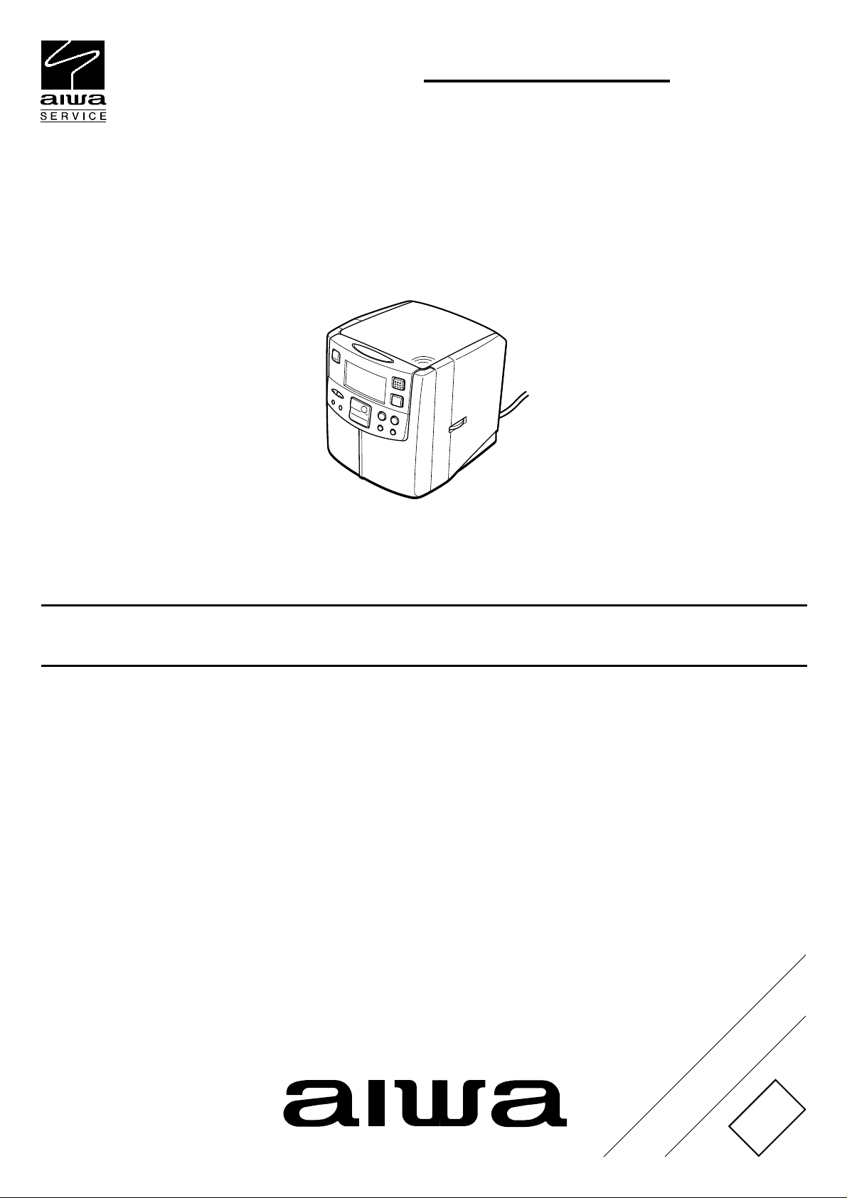
FR-CD2500
U(S),EZ(S)
SERVICE MANUAL
COMPACT DISC STEREO
RADIO RECEIVER
This Service Manual is the "Revision Publishing" and replaces "Simple Manual"
(S/M Code No. 09-015-356-5T1).
BASIC CD MECHANISM : DA11T3C
S/M Code No. 09-015-356-5R1
REVISION
DATA
Page 2
SPECIFICATIONS
<Tuner section>
Frequency range FM: 87.5 – 108 MHz (100 kHz
steps)
AM: 530 – 1,710 kHz (10 kHz
steps)
Antennas FM wire antenna
Ferrite bar antenna for AM
<CD player section>
Tracking system 3-beam laser
Laser pickup Semiconductor laser
D/A conversion 8-times oversampling digital filter
+ 1-bit DAC
Frequency response 20 – 20,000 Hz
<Common section>
Power source AC 120 V, 60 Hz
Output 750 mW + 750 mW (EIAJ)
Power consumption 15 W
Speaker 64 mm, 8 ohms (2)
Maximum outside dimensions (W H D)
156 170 195 mm
(6
1
/46 3/47 3/4in.)
Weight Approx. 1.65 kg (3.6 lbs.)
U MODEL
Design and specifications are subject to change without
•
notice
Design and specifications are subject to change without
•
notice
.
EZ MODEL
.
-2-
Page 3

PROTECTION OF EYES FROM LASER BEAM DURING SERVICING
This set employs laser. Therefore, be sure to follow carefully the
instructions below when servicing.
WARNING!
WHEN SERVICING, DO NOT APPROACH THE LASER EXIT
WITH THE EYE TOO CLOSELY. IN CASE IT IS NECESSARY TO
CONFIRM LASER BEAM EMISSION. BE SURE TO OBSERVE
FROM A DISTANCE OF MORE THAN 30cm FROM THE
SURFACE OF THE OBJECTIVE LENS ON THE OPTICAL
PICK-UP BLOCK.
Caution: Invisible laser radiation when
open and interlocks defeated avoid exposure to beam.
Advarsel:Usynling laserståling ved åbning,
når sikkerhedsafbrydere er ude af funktion.
Undgå udsættelse for stråling.
VAROITUS!
Laiteen Käyttäminen muulla kuin tässä käyttöohjeessa mainitulla tavalla saattaa altistaa käyt-täjän turvallisuusluokan 1 ylittävälle näkymättömälle lasersäteilylle.
VARNING!
Om apparaten används på annat sätt än vad som specificeras i
denna bruksanvising, kan användaren utsättas för osynling
laserstrålning, som överskrider gränsen för laserklass 1.
CAUTION
Use of controls or adjustments or performance of procedures
other than those specified herein may result in hazardous
radiation exposure.
ATTENTION
L'utilisation de commandes, réglages ou procédures autres que
ceux spécifiés peut entraîner une dangereuse exposition aux
radiations.
ADVARSEL!
Usynlig laserståling ved åbning, når sikkerhedsafbrydereer ude
af funktion. Undgå udsættelse for stråling.
This Compact Disc player is classified as a CLASS 1 LASER
product.
The CLASS 1 LASER PRODUCT label is located on the rear
exterior.
CLASS 1
KLASSE 1
LUOKAN 1
KLASS 1
LASER PRODUCT
LASER PRODUKT
LASER LAITE
LASER APPARAT
-3-
Page 4
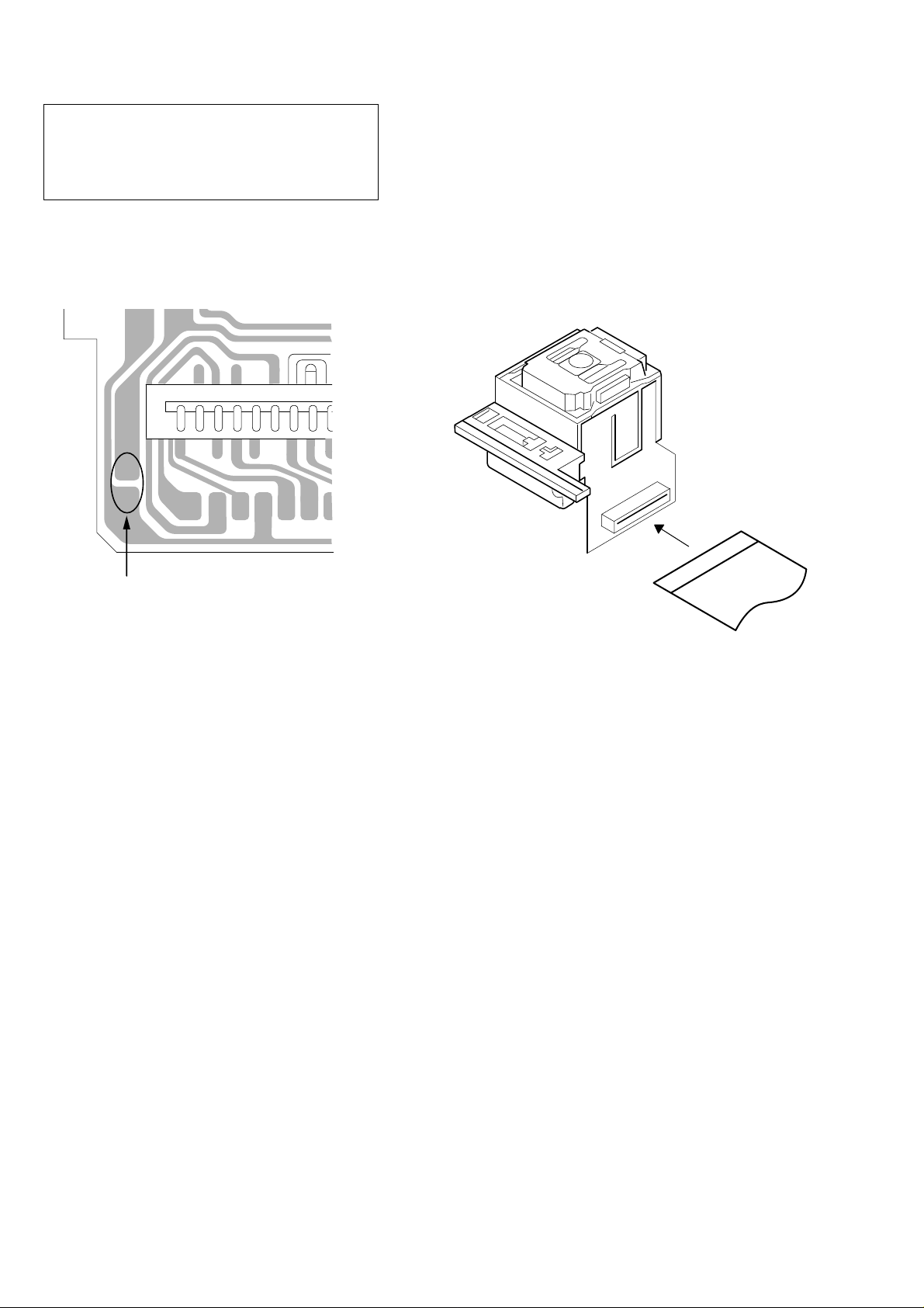
Precaution to replace Optical block
(SF-P101NR)
Body or clothes electrostatic potential could ruin
laser diode in the optical block. Be sure ground
body and workbench, and use care the clothes
do not touch the diode.
1) After the connection, remove solder shown in
the right figure.
PICK UP ASSY
SF-P101NR
Solder
1
16
TO/FROM CD C.B
-4-
Page 5

ELECTRICAL MAIN PARTS LIST-1/3
REF. NO PART NO. KANRI DESCRIPTION
NO.
IC
8A-RU2-606-010 IC,TC9284BF
8A-RU2-605-010 IC,TA2065F
87-A20-157-010 IC,TA2092N
87-A20-754-010 IC,BA4558N-DX
87-A21-184-010 IC,TA2104AN
8B-RD3-627-010 IC,TC9256P
8A-RU2-603-010 IC,TDA2822M
8B-RD3-613-010 IC,TMP87CM24AF
TRANSISTOR
8A-RU2-604-010 TR,3CA8550
8A-RU2-602-010 TR,3DA8050
8B-RD3-607-010 TR,2SB562B
89-318-155-080 TR,2SC1815 (0.4W)
87-026-215-080 TR,DTC114YS
89-414-683-010 TR,2SD1468<CD2500EZSC>
87-026-462-080 TR,2SC1740<CD2500EZSC>
89-501-185-080 TR,2SK118
87-A30-167-010 TR,2SB1566E
87-A30-620-080 TR,DTC114ESA
87-A30-622-080 TR,DTC114YSA
DIODE
87-070-345-080 DIODE,IN4148
87-A40-226-080 VARI-CAP,SVC251SPA
87-017-568-080 VARI-CAP,SVC342M/L
87-A40-398-080 DIODE,1N4001
8B-RD3-633-010 DIODE,RECTIFITERJ-05
87-A40-358-080 ZENER,1N5232B
87-017-105-080 ZENER,HZS7A3
87-A40-029-080 ZENER,RD4.3B1ES
8B-RD3-614-010 ZENER,DIODE3.3V
MAIN C.B
BPF101 8B-RD3-631-010 FLTR,BPF GFMB3-1
C101 87-018-109-080 CAP,TC U 22P-50 J SL UP050
C105 87-018-134-080 CAPACITOR,TC-U 0.01-16
C106 87-018-149-080 CAP,TC U 15P-50 J CH UP050
C107 87-018-143-080 CAP,TC-U 4.7P-50 CH
C108 87-018-125-080 CAP, CER 330P-50V
C109 87-010-544-080 CAP,E 0.1-50 M 11L SME
C110 87-010-401-080 CAP, ELECT 1-50V
C111 87-010-401-080 CAP, ELECT 1-50V
C112 87-010-400-080 CAP,E 0.47-50 M 11L SME
C113 87-010-405-080 CAP, ELECT 10-50V
C114 87-018-205-080 CAP, CERA-SOL 0.022
C115 87-018-132-080 CAP, CER 2200P-16V
C117 87-018-205-080 CAP, CERA-SOL 0.022
C118 87-018-205-080 CAP, CERA-SOL 0.022
C119 87-010-235-080 CAP,E 470-16 SME
C120 87-010-263-080 CAP, ELECT 100-10V
C121 87-018-134-080 CAPACITOR,TC-U 0.01-16
C125 87-018-205-080 CAP, CERA-SOL 0.022
C126 87-018-205-080 CAP, CERA-SOL 0.022
C127 87-010-405-080 CAP, ELECT 10-50V
C128 87-018-209-080 CAP, CER 0.1-50V
C129 87-010-263-080 CAP, ELECT 100-10V
C130 87-018-209-080 CAP, CER 0.1-50V
C131 87-010-400-080 CAP, ELECT 0.47-50V
C132 87-018-205-080 CAP, CERA-SOL 0.022
C133 87-010-544-080 CAP,E 0.1-50 M 11L SME
C134 87-010-544-080 CAP,E 0.1-50 M 11L SME
C135 87-018-205-080 CAP, CERA-SOL 0.022
C136 87-018-205-080 CAP, CERA-SOL 0.022
REF. NO PART NO. KANRI DESCRIPTION
C137 87-010-404-080 CAP, ELECT 4.7-50V
C138 87-018-112-080 CAP,TC U 30P-50 J SL UP050
C139 87-018-112-080 CAP,TC U 30P-50 J SL UP050
C140 87-018-205-080 CAP, CERA-SOL 0.022
C141 87-010-101-080 CAP, ELECT 220-16
C142 87-018-134-080 CAPACITOR,TC-U 0.01-16
C143 87-018-134-080 CAPACITOR,TC-U 0.01-16
C144 87-018-134-080 CAPACITOR,TC-U 0.01-16
C145 87-018-134-080 CAPACITOR,TC-U 0.01-16
C146 87-018-134-080 CAPACITOR,TC-U 0.01-16
C148 87-018-205-080 CAP, CERA-SOL 0.022<CD2500EZSC>
C148 87-018-134-080 CAPACITOR,TC-U 0.01-16<CD2500USC>
C149 87-010-405-080 CAP, ELECT 10-50V
C152 87-018-117-080 CAP,TC U 68P-50 J SL UP050<CD2500EZSC>
C153 87-018-149-080 CAP,TC U 15P50 J CH UP050
C154 87-018-141-080 CAP,TC U 3.3P-50 K CH UP050
C155 87-018-126-080 CAP,TC U 390P-50 K B UP050
C156 87-018-127-080 CAP, CER 470P-50V<CD2500EZSC>
C157 87-018-205-080 CAP, CERA-SOL 0.022<CD2500EZSC>
C157 87-018-201-080 CAP,TC U 5600P-16 N X UP050<CD2500USC>
C158 87-018-134-080 CAPACITOR,TC-U 0.01-16
C159 87-018-134-080 CAPACITOR,TC-U 0.01-16
C161 87-012-286-080 C-CAP,U 0.01-25 K B
C201 87-018-127-080 CAP, CER 470P-50V
C202 87-018-127-080 CAP, CER 470P-50V
C205 87-010-401-080 CAP, ELECT 1-50V
C206 87-010-401-080 CAP, ELECT 1-50V
C207 87-010-401-080 CAP, ELECT 1-50V
C208 87-010-401-080 CAP, ELECT 1-50V
C209 87-018-127-080 CAP, CER 470P-50V
C210 87-018-127-080 CAP, CER 470P-50V
C211 87-010-401-080 CAP, ELECT 1-50V
C212 87-015-997-010 CAP, ELECT 2200UF-16V
C213 87-010-380-080 CAP, ELECT 47-16V
C214 87-010-380-080 CAP, ELECT 47-16V
C215 87-015-997-010 CAP, ELECT 2200UF-16V
C216 87-010-235-080 CAP,E 470-16 SME
C217 87-018-134-080 CAPACITOR,TC-U 0.01-16
C218 87-018-134-080 CAPACITOR,TC-U 0.01-16
C219 87-010-235-080 CAP,E 470-16 SME
C220 87-010-235-080 CAP,E 470-16 SME
C221 87-018-209-080 CAP, CER 0.1-50V
C222 87-018-209-080 CAP, CER 0.1-50V
C223 87-010-405-080 CAP, ELECT 10-50V
C224 87-010-235-080 CAP,E 470-16 SME
C225 87-010-235-080 CAP,E 470-16 SME
C226 87-018-134-080 CAPACITOR,TC-U 0.01-16
C227 87-018-134-080 CAPACITOR,TC-U 0.01-16
C228 87-018-134-080 CAPACITOR,TC-U 0.01-16
C229 87-018-134-080 CAPACITOR,TC-U 0.01-16
C230 87-010-236-080 CAP,E 1000-10 M SME
C231 87-018-205-080 CAP, CERA-SOL 0.022
CF101 87-A91-162-010 FLTR,PFS450A7
CF103 87-A90-991-010 FLTR,SFE10.7 MS239-A
CON202 8B-RD3-621-010 WIRE,ASSY 4P SP
CON203 8B-RD3-619-010 WIRE,CONN 5P 63
!
F201 87-035-428-010 FUSE,2A 125V T 237<CD2500EZSC>
HP201 87-A60-420-010 JACK,3.5 ST (MSC)
L102 8A-RU2-613-010 COIL,FM COIL4T 5MM
L103 8A-RU2-611-010 COIL,FM COIL3T
L104 87-005-239-080 COIL,100UH
L105 87-005-152-080 COIL,10UH
L151 S0-630-041-200 AM COIL 63TÅF0 USTC
L152 S1-750-041-200 LW ANT COIL 175T<CD2500EZSC>
SP1 8A-RU2-662-010 SPKR, F66RZ3201
NO.
-5-
Page 6

ELECTRICAL MAIN PARTS LIST-2/3
REF. NO PART NO. KANRI DESCRIPTION
NO.
SP2 8A-RU2-662-010 SPKR, F66RZ3201
SW417 8B-RD3-639-010 SW,TACT 1120V-4
T103 8A-RU2-607-010 IFT,4A224R
T151 8B-RD3-636-010 COIL,MW OSC3939
T152 8B-RD3-637-010 COIL,LW OSC0644<CD2500EZSC>
TC102 87-011-155-010 CAPACITOR TRIMMER 1P
TC151 87-A91-684-010 TRIMMER,CER 30P 4.0X4.5 ECRLA0
TC152 87-A91-684-010 TRIMMER,CER 30P 4.0X4.5 ECRLA0
<CD2500EZSC>
VR201 8B-RD3-606-010 VR,SL 50KC*2
WH202 8B-RD3-622-010 SOCKET,6P VDD
WH203 8B-RD3-618-010 WIRE,ASSY 6P VDD
X101 87-KTD-602-010 VIB,XTAL 7.2MHZ
CD C.B
C1 87-018-127-080 CAP, CER 470P-50V
C2 87-A10-307-080 CAP,M 0.1-50 J
C3 87-018-208-080 CAP 0.047-50F
C4 87-018-209-080 CAP, CER 0.1-50V
C8 87-018-140-080 CAP,TC U 2.2P-50 K CH UP050
C9 87-010-401-080 CAP, ELECT 1-50V
C12 87-010-404-080 CAP, ELECT 4.7-50V
C13 87-018-110-080 CAP, CERA-SOL SS 24P
C15 87-018-111-080 CAP, CERA-SOL SS 27P
C16 87-010-380-080 CAP, ELECT 47-16V
C17 87-018-208-080 CAP 0.047-50F
C18 87-018-119-080 CAP, CER 100P-50V
C19 87-018-110-080 CAP, CERA-SOL SS 24P
C20 87-010-405-080 CAP, ELECT 10-50V
C21 87-018-133-080 CAPACITOR,CER 4700P-16V
C22 87-018-209-080 CAP, CER 0.1-50V
C23 87-018-209-080 CAP, CER 0.1-50V
C24 87-A10-025-080 C-CAP,U 0.22-16 Z F
C26 87-010-788-080 C-CAP,U 0.033-25 Z F
C27 87-010-382-080 CAP, ELECT 22-25V
C28 87-018-209-080 CAP, CER 0.1-50V
C29 87-010-380-080 CAP, ELECT 47-16V
C30 87-018-208-080 CAP 0.047-50F
C31 87-010-380-080 CAP, ELECT 47-16V
C32 87-018-208-080 CAP 0.047-50F
C33 87-018-134-080 CAPACITOR,TC-U 0.01-16
C34 87-010-263-080 CAP, ELECT 100-10V
C35 87-018-209-080 CAP, CER 0.1-50V
C36 87-018-209-080 CAP, CER 0.1-50V
C37 87-010-405-080 CAP, ELECT 10-50V
C38 87-010-380-080 CAP, ELECT 47-16V
C39 87-018-209-080 CAP, CER 0.1-50V
C40 87-012-274-080 C-CAP,U 1000P-50 K B
C41 87-010-263-080 CAP, ELECT 100-10V
C43 87-010-263-080 CAP, ELECT 100-10V
C45 87-018-209-080 CAP, CER 0.1-50V
C46 87-010-101-080 CAP, ELECT 220-16
C47 87-018-134-080 CAPACITOR,TC-U 0.01-16
C48 87-010-101-080 CAP, ELECT 220-16
C49 87-018-133-080 CAPACITOR,CER 4700P-16V
C50 87-010-405-080 CAP, ELECT 10-50V
C51 87-018-119-080 CAP, CER 100P-50V
C52 87-018-119-080 CAP, CER 100P-50V
C53 87-010-263-080 CAP, ELECT 100-10V
C54 87-010-263-080 CAP, ELECT 100-10V
C55 87-010-404-080 CAP, ELECT 4.7-50V
C56 87-010-404-080 CAP, ELECT 4.7-50V
C57 87-018-111-080 CAP, CERA-SOL SS 27P
C58 87-018-111-080 CAP, CERA-SOL SS 27P
C59 87-018-119-080 CAP, CER 100P-50V
REF. NO PART NO. KANRI DESCRIPTION
NO.
C60 87-018-119-080 CAP, CER 100P-50V
C61 87-010-263-080 CAP, ELECT 100-10V
C62 87-018-134-080 CAPACITOR,TC-U 0.01-16
C63 87-018-209-080 CAP, CER 0.1-50V
C64 87-018-209-080 CAP, CER 0.1-50V
C65 87-010-263-080 CAP, ELECT 100-10V
C66 87-018-209-080 CAP, CER 0.1-50V
C68 87-010-405-080 CAP, ELECT 10-50V
C69 87-018-209-080 CAP, CER 0.1-50V
C71 87-018-209-080 CAP, CER 0.1-50V
C73 87-018-127-080 CAP, CER 470P-50V
C74 87-018-127-080 CAP, CER 470P-50V
C80 87-010-405-080 CAP, ELECT 10-50V
CN1 8B-RD3-609-010 SOCKET,16P FFC
CN2 8B-RD3-610-010 SOCKET,2P HEADER
CON1 8B-RD3-608-010 CABLE,FFCP-16 L-65
CON444 8B-RD3-638-010 SOCKET,10P CD
CX101 8A-RU2-632-010 FLTR,16.93M RESONATOR
JW3 S0-102-260-000 INDUCTOR 22UH
L1 87-005-239-080 COIL,100UH
L2 87-005-239-080 COIL,100UH
L3 8A-RU2-634-010 COIL,CORE100MHZ
L11 87-005-239-080 COIL,100UH
L12 8A-RU2-634-010 COIL,CORE100MHZ
R72 87-018-119-080 CAP, CER 100P-50V
VR1 8A-RU2-631-010 SFR, KVSF637AB
VR2 8A-RU2-630-010 SFR,100K EVND8AV06P
WH2 8B-RD3-610-010 SOCKET,2P HEADER
CONTROL C.B
B201 8B-RD3-616-010 LAMP,8V 60MA
B202 8B-RD3-616-010 LAMP,8V 60MA
C401 87-010-831-080 C-CAP,U,0.1-16F
C402 87-010-831-080 C-CAP,U,0.1-16F
C403 87-010-831-080 C-CAP,U,0.1-16F
C404 87-015-695-080 CAP,E 1-50 M 7L SRA
C405 87-010-787-080 CAP, U 0.022-25
C406 87-012-183-080 C-CAP,U 30P-50CH
C407 87-012-183-080 C-CAP,U 30P-50CH
C408 87-012-199-080 C-CAP,U 220P-50 J CH
C409 87-012-184-080 C-CAP,U 33P-50 J CH
C410 87-012-184-080 C-CAP,U 33P-50 J CH
C411 87-010-831-080 C-CAP,U,0.1-16F
C415 87-010-831-080 C-CAP,U,0.1-16F
C416 87-010-526-040 CAP,E 120-16 M 105 SXE
C417 87-010-831-080 C-CAP,U,0.1-16F
C418 87-015-680-080 CAP,E 47-10 M 7L SRA
C441 87-012-199-080 CAP,U 220P-50 J CH
C442 87-012-282-080 C-CAP,U 4700P-50 K B
C443 87-012-286-080 C-CAP,U 0.01-25 K B
C444 87-012-286-080 C-CAP,U 0.01-25 K B
C445 87-018-205-080 CAP, CERA-SOL 0.022
C446 87-018-208-080 CAP 0.047-50F
CON402 S1-300-572-000 CONN, 13P
DP401 8B-RD3-615-010 LCD,CD TUNERBRD-3
JW427 S7-006-307-080 COIL 220UH
JW433 S7-006-307-080 COIL 220UH
SW401 8A-RU2-623-010 SW,TACT 5MM
SW402 8A-RU2-623-010 SW,TACT 5MM
SW403 8A-RU2-623-010 SW,TACT 5MM
SW404 8A-RU2-623-010 SW,TACT 5MM
SW406 8A-RU2-623-010 SW,TACT 5MM
SW407 8A-RU2-623-010 SW,TACT 5MM
SW408 8A-RU2-623-010 SW,TACT 5MM
SW409 8A-RU2-623-010 SW,TACT 5MM
-6-
Page 7
ELECTRICAL MAIN PARTS LIST-3/3
REF. NO PART NO. KANRI DESCRIPTION
NO.
SW410 8A-RU2-623-010 SW,TACT 5MM
SW411 8A-RU2-623-010 SW,TACT 5MM
SW412 8A-RU2-623-010 SW,TACT 5MM
SW413 8A-RU2-623-010 SW,TACT 5MM
SW414 8A-RU2-623-010 SW,TACT 5MM
SW415 8A-RU2-623-010 SW,TACT 5MM
SW416 8B-RD3-639-010 SW,TACT 1120V-4
SW417 8A-RU2-623-010 SW,TACT 5MM
X401 87-A70-047-080 VIB,CER 4MHZ EFOEC4004T4
X402 87-A70-170-010 VIB,XTAL 32.768KHZ
REF. NO PART NO. KANRI DESCRIPTION
POWER C.B
!
J1 8A-RU2-664-010 AC CORD, SPT-2
!
PT1 8A-RU2-663-010 TRANS, 120/10<CD2500USC>
MOTOR C.B
M2 S0-M10-A09-700 MOTOR SLED ASSY
PIN3 S2-369-750-000 PLUG,6P
SW1 S4-S13-A01-600 SW,LEAF
NO.
• Regarding connectors, they are not stocked as they are not the initial order items.
The connectors are available after they are supplied from connector manufacturers upon the order is received.
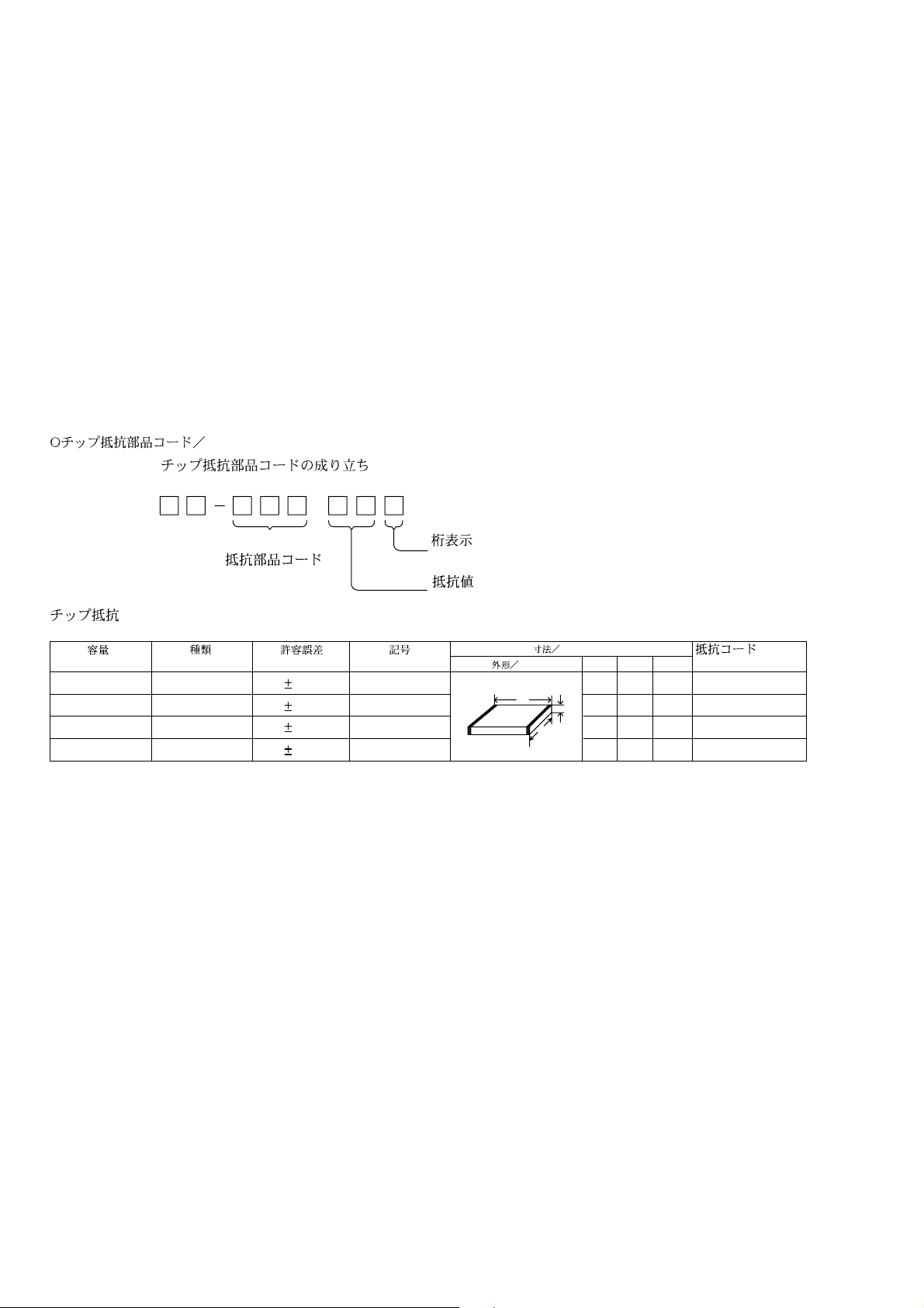
CHIP RESISTOR PART CODE
Chip Resistor Part Coding
88
A
Resistor Code
Figure
Value of resistor
Chip resistor
Wattage Type Tolerance
1/16W 1005 5% CJ
1/16W
1/10W
1/8W
1608
2125
3216
5%
5%
5%
Symbol
CJ
CJ
CJ
Form
L
W
Dimensions (mm)
LW t
1.0 0.5 0.35 104
t
1.6 0.8 0.45
2 1.25 0.45
1.6
0.55
3.2
Resistor Code
108
118
128
: A
: A
-7-
Page 8

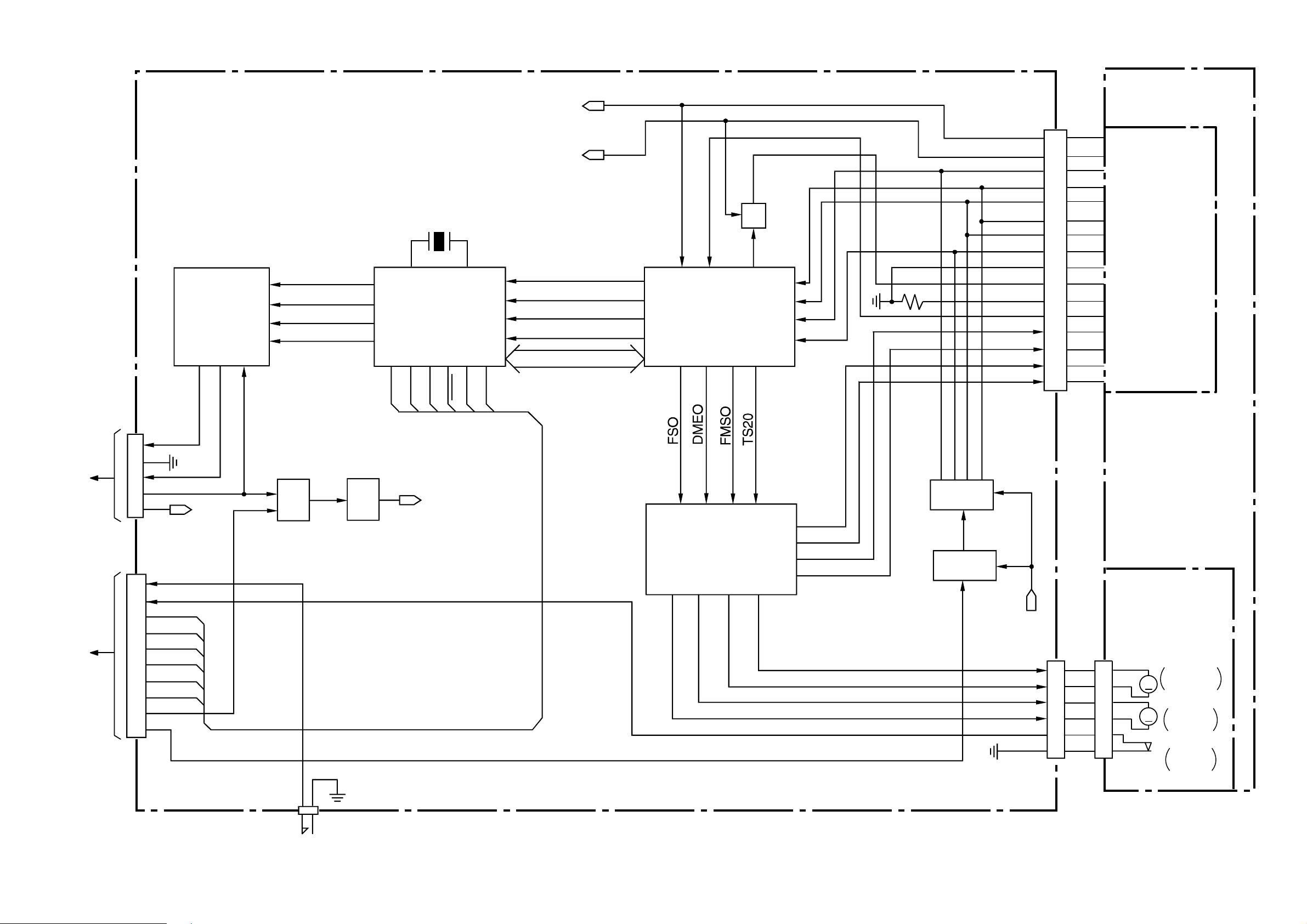
BLOCK DIAGRAM-1/2 (TUNER / AMP & CPU SECTION)
MAIN C.B
FM OSC
D103
L103
CON444
TO CD C.B
FM RF
D104
TC102,L102
MW RF
L151,TC151
LW RF
L152,TC152
EZ
MW OSC
T151
LW OSC
T152
VAREF
P57
P56
P55
48
47
46
445
CD_DOOR
1
PUIN
2
CCE
3
BUCK
4
BUS3
5
BUS2
6
BUS1
7
BUS0
8
CD_ON
9
CD_RW
10
CON401
EZ
RESET
KEY
MATRIX
CONTROL C.B
FM-RF-OUT
Q15
3
Q152
FM
ANT
BPF101
Q151
LCD DISPLAY
DP401
23
63-9533-41
52
51
CPU
IC401
TMP87CM24
12 18 19 20 21 22 24 25
PWR-ON
TU-CLK
TU-DATA
TU-PERIOD
MONO-SW
ATTN1
FM-STEREO
Q401
FM-OSC
AM-OSC
AM-RF-IN
24 22 17
AM/IF RF IF MPX
ST-LED
2021 18 19
IC101TA2104AN
42567111
MIX-
OUT
FM-
RF-IN
T103
VCC
AM-
IF-IN
CF101
FM-
IF-IN
B201
B202
MUTE
LAMP+
BACK_UP
VCC
42
BUZZER
ATTN2
Q405
Q404
TO CD C.B
CON3
OSC-OUT
IF-REQ
R-OUT
CF103
7
2
3
4
5
6
1
8
9
10
11
12
13
CON402
LPF2
13
LPF1
14
2
VCC
L-OUT
CON443
7
LAMP+
2
BACK UP
3
+16V
4
5
6
POR-ON
1
FM-ST
8
MONO-ST
9
TUN-PERIOD
10
TUN-CLK
11
TUN-DATA
12
13
CON203
1
2
3
4
5
MUTE
RESET
CD-L
CD-R
VCC
Q104
+8V
Q107
Q105
Q106
Q102
Q103
Q205
Q206
DZ232
Q207
DZ201
Q203
Q204
DZ202
DO1
FM-ON
BUZZER
FMIN
IFIN
15 13 11 10 9
7
8
PLL
IC102 TC9256P
123456
XT
X101
7.2MHz
XT
PERIOD
LW/MW
2
POWE
6
8
7
R
AMP
IC201
TDA2822M
RECTIFIER
D211,D212
RECTIFIER
D207~D210
DZ231
AMIN
VDD
DATA
CLOCK
TUN-ON
Q108
HEADPHONE
JACK
HP201
WH201 CN203
1
1
2
2
3
3
4
4
5
5
6
6
1
1
2
2
3
3
4
4
WH202 CON202
TRANSFORMER
6F22x1
DC 9V
Clock Back up
SPR1
SPR2
AC~
U : AC 120V 60Hz
EZ : AC 230V 50Hz
-8-
POWER C.B
Page 9
BLOCK DIAGRAM-2/2 (CD SECTION)
CD C.B
AUDIO
FILTER
IC4
BA4558
178
VCC
OUT2
OUT1
CON3
CD_L
1
2
3
CON203
TO MAIN C.B
4
5
CON444
1
2
3
4
5
CON401
6
7
TO CONTROL C.B
8
9
10
CD_R
CD_8V
CDGND
CD_DOOR
PUIN
CCE
BUCK
BUS3
BUS2
BUS1
BUS0
CD_ON
CDR/W
CD MECHANISM
DA11T3C
+5V
CN1
+2.5V
1
+5V
VREF
2
E
3
D
4
A
OPTICAL
PICK UP
SF-P101NR
5
Q1
MDI
XO XI
+IN2
5
-IN2
6
-IN1
2
+IN1
3
/RO
RO
/LO
LO
79 78
3
2
5
TC9284B
6
DSP
IC1
53
51
50
F
38
14 15 16 17 18 19
CCE
BUCK
Q4
Q3
Q2
DZ1
BUS1
BUS0
BUS3
BUS2
+5V
RFI
RFRP
SBAD
DMON
SERVO SIGNAL
TC9284B
RFO
RFRP
SBAD
DMEN
VRO
346 45
1
5
ASP
6
23
TA2065BF
16 24 26 30
20 17 8 5
LDO
IC2
DRIVER
IC3
TA2092N
44
43
41
40
23
2
4
FPI
FNI
TNI
TPI
Q5~Q8
Q9
B
C
F
GND
LD
VR
PD
F+
T+
TF-
6
7
8
9
10
11
12
13
14
15
16
21
9111416
VRE
CN2
DM+
DM-
FM+
FM-
SLT
GND
F
1
2
3
4
5
6
MOTOR
C.B
PIN3
M
M
+
-
+
-
1
2
3
4
5
6
M3
SPINDLE
MOTOR
M2
SLED
MOTOR
S1
INSIDE
LIMIT
WH2
CD DOOR SW
-9-
Page 10
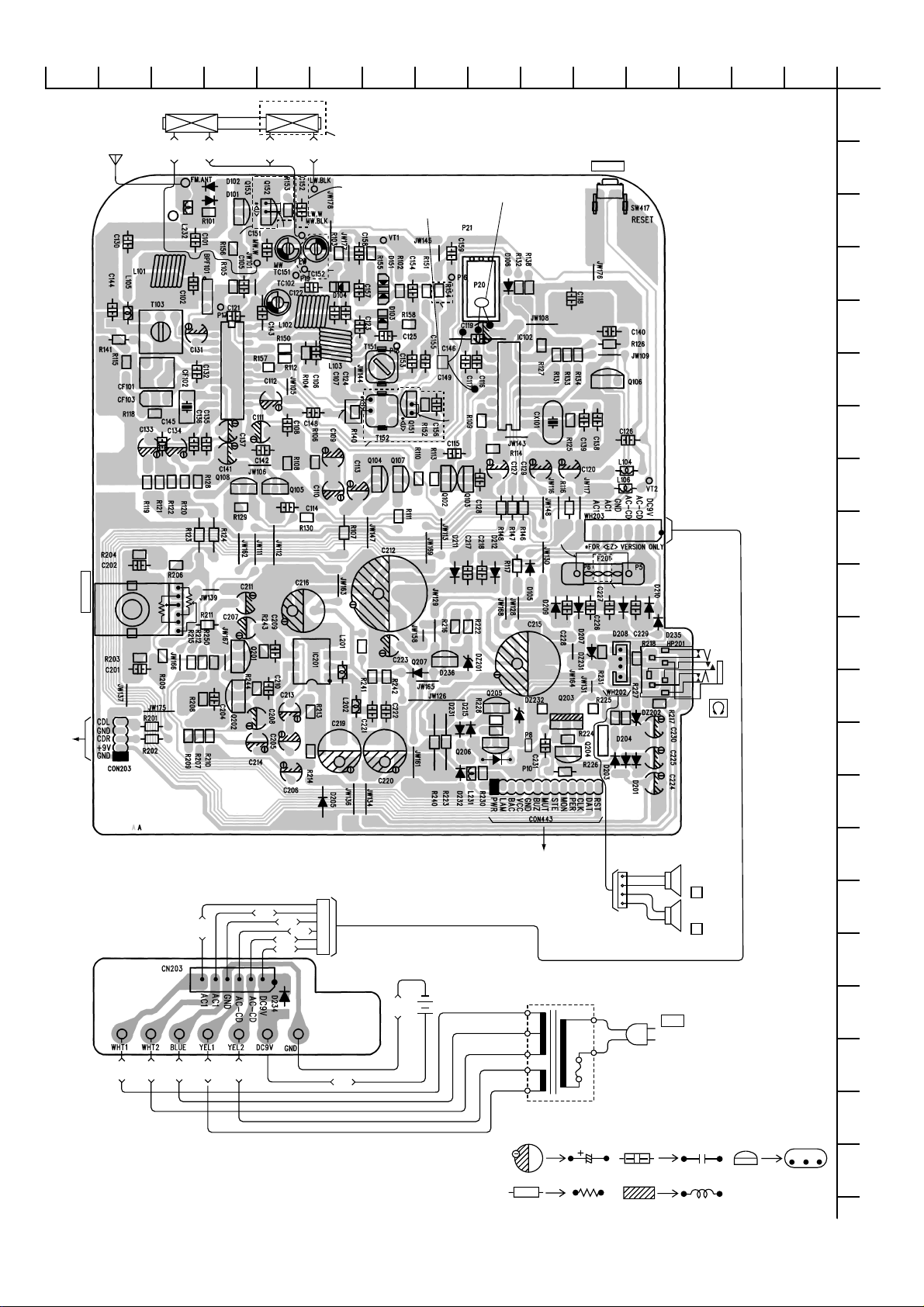
WIRING-1/3 (MAIN, POWER)
123456789101112131415
FM ANT
L151 (MW) L152 (LW)
WHT
BLK
SGD
124
619
WHT
U
JW2
EZ
IC101
12 13
BLK
MAIN C.B
EZ
EZ
C149
INSERTED PARTS SIDE
EZ
EZ
(INSERTED PARTS)
SW417
RESET
C161
CHIP PARTS SIDE
A
B
C
D
E
98
JW1
U
EZ
13 4
U
16 1
F
G
H
U
136
I
VOLUME
VR201
TO CD C.B CON3
VR201
1
4
5
POWER C.B
R221
4
5
1
8
(INSERTED PARTS)
BLU
YEL
YEL
BLU
6
5
4
3
2
1
BLK
BLK
RED
631
6F22x1
DC 9V
clock battery
back up
R219
P12
D216
P11
C232
1
2 5 10 13
TO CONTROL C.B
CON402
PT1
EZ
1
4
1
4
CON202
2.5 inch 8
~
AC
SP1
SP2
J
K
HP201
L
M
N
O
1W
L
P
1W
R
Ω
Q
R
WHT
WHT
BLU
YEL
YEL
RED
-10-
NOTE
Rxxx Rxxx
U: AC120V 60Hz
EZ: AC230V 50Hz
Cxxx
Cxxx
ECB
S
T
ECB
U
Page 11

SCHEMATIC DIAGRAM-1/3 (MAIN, POWER)
MAIN C.B
EZ MODEL
VT ADJUSTMENT :
MW : LOW END IS 0.9V
LW : LOW END IS 1.0V
FM : LOW END IS 2.0V
L151,TC151 MW TRACKING ADJ.
MW COIL
63T
LW COIL
L152,TC152
LW TRACKING ADJ.
GFMB3
AM/FM RF IF
MW OSC
FM FREQ
RANGE ADJ.
U
MODEL
IC101
MPX
LW SW
L102,TC102 FM TRACKING ADJ.
MW RF AMP
L103 FM FREQ.RANGE ADJ.
10P
50V
AM IF
R104
1K
Ref. No.
C148
C157
EZ
U
0.02uF
0.01uF
0.02uF
5600P
4.7K
2.2K
1UF
0.1UF
50V
50V
22
50V
3.3K
50
C133
0.1UF
50V
50V
C134
0.1UF
50V
BAND
50V
50V
1.8K
3.3K
3.3K
1.8K
3.3K
3.3K
47K
10V
8.2K
C159
0.01
10V
1.5K
50V
VT
CX101
C149
10UF/50V
C161
0.01
PLL
4.7K
470UF
1.2K
10V
10V
CON402
TO CONTROL C.B
CON3
TO CD C.B
LW SW
C231
0.022
LW OSC
LW FREQ
ADJ.
EZ MODEL
1UF 50V
POWER AMP
3.3K
4.7K
6.8K
6.8K
220uH
1UF 50V
VOLUME
VOLUME
VA SW
R228
47K
EZ
MODEL
WH203 CN203
PT1
POWER C.B
BAT1
6F22x1
DC9V
Ciock baattery
back up
SP1
SP2
AC~
U : AC 120VB 60Hz
EZ : AC230V 50Hz
-11-
R230 1K
SIGNAL
FM/PB
AM
Page 12
WIRING-2/3 (CD, MOTOR)
123456789101112131415
LEAF SW
CD C.B
(INSERTED PARTS)
1
2
1
2
OPTICAL PICK UP
SF-P101NR
16
10
15
MOTOR C.B
A
(CONDUCTOR SIDE)
M2
_
+
6
PIN3
1
1
24
5
20
125
15
10
12
13
M2
(SLED MOTOR)
SW1
(INSIDE LIMIT SW)
(SPINDLE MOTOR)
SW1
_
M3
6
1
M3
B
C
D
+
E
F
G
H
I
1
CON401
CONTROL C.B
J
C67
48
39
38
25
24
1
R73
14
15
U
EZ
K
L
M
N
2
5
10
41
40
25
24
64
65
80
1
8
4
1
1
5
TO CONTROL C.B
CON203
MAIN C.B
O
P
Q
R
Note
RXX RXX
CXX CXX
S
-12-
ECB
ECB
T
U
Page 13

SCHEMATIC DIAGRAM- 2/3 (CD, MOTOR)
CD C.B
AUDIO FILTER
2.2M
VR1
RF ADJ.
R/W SW
Q8
2SC1815GR
4.7
R72 3.9K
C67 100P
R74 3.9K
2.2PF
10V
LD AMP
VR2
EF BALANCE ADJ.
270K
240K
120K
68K
68K
68K
68K
120K
CD MECHANISM
DA11T3C (1/2)
CN1CON1
CON203
TO MAIN C.B
CON401
TO CONTROL C.B
50V
0.01U
3.3K3.3K
50V
10V
10V
10V
10V
Q2-4
REG
10V
DSP
1.5M
16V
4700P
R/W SW
Q10
2SC1815GR
R68
10K
50V
R73
100K
16V
16V
16V
3.9K
2.7K
1.2K
50V
10K
R6
C25
0.039UF
4.7uF
50V
ASP
C40
1000P
50V
4.7K
25V
2.2M
2.2K
2.2K
10K
12K
4.7K
680
R76
R75
180K
R60
10K
270K
R89
10K
Q5
2SC1815GRQ62SC1815GRQ72SC1815GR
R59
10K
R85
4.7
R78 10K
R77
47K
Q9
2SC1815GR
R72
10K
R70
47K
++
–
–
OPTICAL
PICK UP
SF-P101NR
COIL
TRACKING
Q5-7,9
R/W SW
CN2
COIL
FOCUS
CD MECHANISM
DA11T3C (2 /2)
++–
M
PIN3
1
2
3
4
M
5
–
6
MOTOR
C.B
M3
SPINDLE
MOTOR
M2
SLED
MOTOR
S1
INSIDE
LIMIT
CON444
LEAF
SW
R91
1K
330
JW3
Ref. No.
JW3U22uHEZJW
10V 10V
-13-
10V
DRIVER
RXX
RXX
SIGNALNOTE
: PB
Page 14

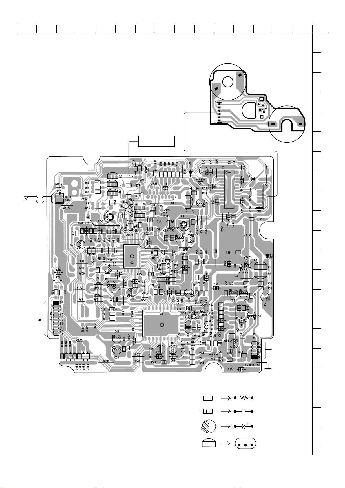
WIRING-3/3 (CONTROL)
CONTROL C.B
SW410
POWER
STAND BY/ON
(INSERTED PARTS)
SW416
SNOOZE
SW413
FUNCTION
SW412
BAND/
SUMMER.T/DST
123456789101112131415
A
B
C
C415
R482
R411
1
2
R427
R428
5
R431
R430
R429
10
CD C.B CON444
R479
EZ
EZ
R465
U
R466
R409
R421
C417
51
50
75
IC401
26
25
R464
R463
R467
Q403
R407
R412
R462
13 10 5 2
C411
R408
C407
C409
C408
1
C410
C406
C445
R426
76
100
R417
28
R474
R475
R476
R472
C401
C402
C403
121
C405
Q401
R418
R401
JW424
1
R410
C444
DP401 (1/2) (LCD DISPLAY)
R420
C443
C442
C441
Q404
Q405
22
R470
R473
R471
R477
R413
R425
DP401 (2/2)
R419
R422
R416
R414
R424
R423
R415
C446
D
E
F
G
H
I
J
K
L
MAIN C.B CON443
SW401
RANDOM/
DOWN
SW406
SET
SW402
REPEAT/
UP
SW407
FM STEREO
SW409 SW411
SW414
SW415
SW403
ALARM 1
SW408
SLEEP
ALARM 2
WEEKEND
ALARM SKIP
NOTE
Rxxx
Rxxx
Cxxx
SW404
SW417
Rxxx
Cxxx
M
N
O
P
ECB
Q
R
S
T
U
-14-
Page 15

SCHEMATIC DIAGRAM-3/3 (CONTROL)
CONTROL C.B
90980TT
PM18
PM19
PM20
CPU
PM21
1.5K
RANDOM/
DOWN
JW427
220uH
SET
POWER
STANDBY/ON
120/16V
REPET/
UP
1.5K
1.5K 2.2K
2.2K
2.2K
BAND/
SUMMER.T/DST
3.3K
3.3K
3.3K
FUNCTION
5.6K
ALARM SKIP
5.6K
5.6K
50V
RESET
4MHz
220P
CLK
SHIFT
33P
33P
U
MODEL
EZ
MODEL
Q404,405
BUZER SW
JW433
220uH
10V
C446
0.047U
C444
0.01U
C445
0.022U
RESET
CON444
TO CD C.B
CON443
TO MAIN C.B
-15-
Page 16

TRANSISTOR ILLUSTRATION-1/1
C
ECB ECB ECB
2SC1815
2SD1468
BCE
2SB1566
2SC1740
DTC114YS
ECB
3CA8550
2SB562B
S G D
2SK118
3DA8050
B
E
DTC114ESA
DTC114YSA
-16-
Page 17

IC BLOCK DIAGRAM-1/1
IC, BA4558N
IC, TA2104AN
FM RF OUT
24 23 22 21 20 19 18 17 16 15 14 13
RF VCC AM RF IN FM OSC AM OSC OSC OUT ST LED IF REQ DET OUT LPF1 LPF2
IF
REQ
AM
DET
AF
BUFF
AGC
FM
DET
AF
ST/MO
FM/AM
FM
RF
AM
MIX
FM
OSC
FM
MIX
AM
OSC
BUFF
BUFF
LEVEL
DET
AMIF
ST
SW
IF
BUFF
1/8
FMIF
VCO
DIVIDE
DECODE
MUTE
RF GND FM RF IN AM IF IN FM IF IN GND AGC QUAD R-OUT L-OUTAM LOW
CUT
1110987654321 12
MIX OUT VCC
-17-
Page 18

ELECTRICAL ADJUSTMENT-1/3 (TUNER SECTION : U)
<
TUNER SECTION : U MODEL
MAIN C.B
MW COLL
L151
3
T103
1
35
1
test point
TC151
16
>
TC102
L103
IC101
L102
T151
R102
2
test point
4
5
2
4
1. AM IF Adjustment
Test point: IC101 (TA2104AN) 16PIN
Adjustment location: T103
T103 ...……..........… 450kHz
2. MW Frequency Range Adjustment
Test point: R102
Adjustment location: T151
Set tuner frequency to be 530kHz
Adjust T151 so that voltage of test
point is 0.9V
3. MW Tracking Adjustment
Test point: IC101 (TA2104AN) 16PIN
Adjustment location: L151, TC151
L151 ............……… 600kHz waveform max.
TC151 ..……...….… 1404kHz waveform max.
4. FM Frequency Range Adjustment
Test point: R102
Adjustment location: L103
Set tuner frequency to be 87.5 MHz
Adjust L103 so that voltage of test point
is 2.0 V
5. FM Tracking Adjustment
Test point: IC101 (TA2104AN) 16PIN
Adjustment location: L102, TC102
L102 .........……...… 90.1MHz waveform max.
TC102 ....……....… 106.1MHz waveform max.
-18-
Page 19

ELECTRICAL ADJUSTMENT-2/3 (TUNER SECTION : EZ)
<
TUNER SECTION : EZ MODEL
MAIN C.B
3
T103
1
16
1
357
test point
>
MW COLL
L151 L152
TC151 TC152
TC102
L103
IC101
LW COLL
R102
L102
T151
T152
46
2
test point
5
7
2
4
6
1. AM IF Adjustment
Test point: IC101 (TA2104AN) 16PIN
Adjustment location: T103
T103 .....................… 450kHz
2. MW Frequency Range Adjustment
Test point: R102
Adjustment location: T151
Set tuner frequency to be 531kHz
Adjust T151 so that voltage of test
point is 0.9V
3. MW Tracking Adjustment
Test point: IC101 (TA2104AN) 16PIN
Adjustment location: L151, TC151
L151 .....….....…..… 603kHz waveform max.
TC151 ..…...........… 1404kHz waveform max.
4. LW Frequency Adjustment
Test point: R102
Adjustment location: T152
Set tuner frequency to be 144kHz
Adjust T152 so that voltage of test
point is 0.9 V
5. LW Tracking Adjustment
Test point: IC101 (TA2104AN) 16PIN
Adjustment location: L152, TC152
L152 ....................….. 144kHz
TC152 ....................… 281kHz
6. FM Frequency Range Adjustment
Test point: R102
Adjustment location: L103
Set tuner frequency to be 87.5MHz
Adjust L103 so that voltage of test
point is 2.0 V
7. FM Tracking Adjustment
Test point: IC101 (TA2104AN) 16PIN
Adjustment location: L102, TC102
L102 .....…...…....… 90.1MHz waveform max.
TC102 ......…...……. 106.1MHz waveform max.
-19-
Page 20

ELECTRICAL ADJUSTMENT-3/3 (CD SECTION)
<
CD SECTION
CD C.B
2
2
>
TSO
VR2
JW35
IC2
VR1
1
RF
C17
3
1
test point
VREF
1. RF Adjustment
Test point: RF (IC2 1PIN) and VREF (IC2 3PIN)
1) Connect the oscilloscope to the test points.
2) Turn on power switch.
3) Load test disc (TDC-782) and play the second track.
4) Adjust VR1 so that RF waveform is maximum.
5) Turn off power switch.
2. EF Balance Adjustment
Test point: TSO (IC2 35PIN) and VREF (IC2 3PIN)
1) Connect an oscilloscope to the test points.
2) Turn on power switch.
3) Load test disc (TCD-782) and play.
4) Press skip button so that EF
waveform appears.
5) Adjust VR2 so that EF waveform is symmetrical.
6) Turn off power switch.
-20-
Page 21

VOLTAGE CHART-1/2
(
)
)
)
(
)
)
(
)
)
)
(
)
)
THE MEASURED VALUE IS DC VOLTAGE
UNIT: V
TUNER SECTION
TEST CONDITION:SET AM/FM TUNER ON ONE FREQUENCY
IC101 (TA2104AN)
PIN'S NUMBER 123456789101112
AM 0 0 1.15 5.68 5.73 5.05 5.73 0 0.45 5.15 1.26 1.25
FM 0 0.78 0.15 4.33 4.57 4.03 4.60 0 0.49 3.81 1.23 1.20
PIN'S NUMBER 13 14 15 16 17 18 19 20 21 22 23 24
AM 0 0 0.70 1.17 0.97 5.99 5.56 5.72 5.73 5.70 5.73 5.73
FM 3.93 3.89 0.70 1.34 0.71 0.10 4.42 4.56 4.92 4.55 4.56 4.85
IC102 (TC9256P)
PIN'S UNMBER 12345678
AM 2.73 2.76 5.49 5.48 5.50 0.11 0.26 0
FM 2.72 2.75 5.49 5.49 5.48 0.09 5.00 0
PIN'S UNMBER 9 10 11 12 13 14 15 16
AM 5.50 2.78 0 0 2.73 0 1.20 4.38
FM 5.48 0 2.72 0 2.72 0 1.18 2.33
TRANSISTOR Q102
ECBECBECB
AM 0 0.92 0.61 0.62 0.92 11.9 0 0 0.67
FM 0 4.55 0.61 0.61 4.55 1.18 0 3.87 0.02
TRANSISTOR Q105
ECBECB
AM 0 0 3.12 0 3.11 0.25
FM 0 3.93 0 0 0 4.58
C1815
DTC114YS
Q103 (C1815
Q106 (DTC114YS
Q104 (C1815
POWER & AMP.
TEST CONDITION:CD PLAY
IC201 (TDA2822M)
PIN'S NUMBER 12345678
CD PLAY 3.93 8.84 3.96 0 0.53 0 0 0.53
TRANSISTOR Q203
ECBECBECB
CD 8.48 6.40 7.85 5.70 7.85 6.32 4.66 8.95 5.17
TRANSISTOR Q205
ECBECB
CD 9.78 8.84 9.13 6.87 9.85 6.21
B1566E
8550C
Q204 (C1815
Q207 (8050
Q206 (C1815
CD SECTION
TEST CONDITION: CD PLAY
IC2 (TA2065F)
PIN'S NUMBER 123456789101112
1.88 2.07 2.07 1.92 2.19 2.00 2.00 2.06 2.06 1.87 1.86 1.83
PIN'S NUMBER 13 14 15 16 17 18 19 20 21 22 23 24
1.82 2.07 2.07 2.09 2.18 2.45 0 4.89 2.02 2.11 2.11 2.21
PIN'S NUMBER 25 26 27 28 29 30 31 32 33 34 35 36
1.83 2.05 2.06 2.07 1.84 2.07 2.05 2.06 2.07 2.07 2.07 2.07
PIN'S NUMBER 37 38 39 40 41 42 43 44 45 46 47 48
0.14 2.07 1.89 2.05 2.03 1.91 2.07 2.06 3.84 0.18 2.07 1.91
IC3 (TA2092N)
PIN'S NUMBER 123456789101112
0 3.99 8.67 4.12 2.09 2.07 4.05 2.05 3.95 8.67 4.19 0
PIN'S NUMBER 13 14 15 16 17 18 19 20 21 22 23 24
0 3.60 8.65 4.48 2.22 0 8.65 2.07 4.04 8.66 4.06 0
-21-
Page 22

VOLTAGE CHART-2/2
(
)
)
)
IC1 (TC9284BF)
PIN'S NUMBER 123456789101112
0 2.95 2.81 4.89 2.80 2.56 0 4.86 4.86 4.87 4.89 4.89
PIN'S NUMBER 13 14 15 16 17 18 19 20 21 22 23 24
0 4.37 4.28 4.28 4.29 4.22 4.6 2.27 4.88 0.08 0 0
PIN'S NUMBER 25 26 27 28 29 30 31 32 33 34 35 36
4.89 0 0 2.07 2.07 0 0.28 2.08 1.69 2.07 4.86 1.79
PIN'S NUMBER 37 38 39 40 41 42 43 44 45 46 47 48
4.86 2.07 2.07 2.29 4.14 4.86 2.43 2.44 2.07 2.06 2.06 0.31
PIN'S NUMBER 49 50 51 52 53 54 55 56 57 58 59 60
2.07 2.00 2.19 2.07 0.35 0 0.38 4.89 2.36 4.89 4.89 2.08
PIN'S NUMBER 61 62 63 64 65 66 67 68 69 70 71 72
1.98 2.07 1.95 1.31 0 4.87 0 0 1.22 1.62 2.43 2.43
PIN'S NUMBER 73 74 75 76 77 78 79 80
2.52 0 2.42 4.85 4.89 2.16 1.91 2.21
IC4 (BA4558N)
PIN'S NUMBER 12345678
CD PLAY 5.57 5.20 4.99 0 5.00 5.20 5.82 8.45
TRANSISTOR Q2
ECBECBECB
CD 4.48 6.26 5.58 0 0.08 0.74 6.35 6.26 5.51
8050
Q3 (8050
Q4 (B562
CPU SECTION
TEST CONDITION: CD PLAY OR BUZZER ON
IC401 (TMP87CM24AF)
PIN'S NUMBER 123456789101112
CD 0 2.26 1.95 5.30 3.05 2.36 0 0.95 3.18 0.16 0 5.39
BUZZER ON 0 2.29 1.99 5.37 3.10 2.23 0 0.95 3.18 0.96 2.40 5.40
PIN'S NUMBER 13 14 15 16 17 18 19 20 21 22 23 24
CD 0 0 0 5.40 5.40 5.60 5.40 5.40 0.02 5.91 0.03 0.01
BUZZER ON 0 0 0 5.45 5.45 5.63 5.47 5.46 0 5.90 0.03 5.45
PIN'S NUMBER 25 26 27 28 29 30 31 32 33 34 35 36
CD 0.15 0.01 5.41 5.41 5.41 5.83 5.91 5.91 5.20 4.30 4.40 4.30
BUZZER ON 5.45 0.01 5.47 5.47 5.45 5.87 5.95 5.95 0.01 0.01 0.01 0.01
PIN'S NUMBER 37 38 39 40 41 42 43 44 45 46 47 48
CD 4.36 4.60 4.19 5.72 0.07 0.06 0.03 0.03 5.89 5.89 5.89 6.20
BUZZER ON 0.01 0.01 0.01 0.02 0.04 0.04 0 0 5.94 5.94 5.94 6.20
PIN'S NUMBER 49 50 51 52 53 54 55 56 57 58 59 60
CD 0 0 5.43 5.43 2.39 0 1.40 1.40 1.40 1.40 1.40 1.40
BUZZER ON 0 0 5.48 5.48 1.39 0 1.40 1.40 1.40 1.40 1.40 1.40
PIN'S NUMBER 61 62 63 64 65 66 67 68 69 70 71 72
CD 1.40 1.40 //////////
BUZZER ON 1.40 1.40 //////////
PIN'S NUMBER 73 74 75 76 77 78 79 80 81 82 83 84
CD ////////////
BUZZER ON ////////////
PIN'S NUMBER 85 86 87 88 89 90 91 92 93 94 95 96
CD ///////////2.76
BUZZER ON ///////////2.76
PIN'S NUMBER 97 98 99 100
CD 1.86 1.63 0.70 0
BUZZER ON 1.86 1.65 0.70 0
-22-
Page 23

FL (90980TT) GRID ASSIGNMENT/ANODE CONNECTION-1/1
GRID ASSIGNMENT
ANODE CONNECTION
-23-
Page 24

IC DESCRIPTION-1/4 (TC9256P)-1/1
Pin No. Pin Name I/O Description
1
2
3
4
5
6
XT
______
XT
PERIOD
CLOCK
DATA
TUN-ON
O
I/O
O
Crystal ocsillator pins. Connect 7.2MHz crystal oscillator to supply reference frequency and
I
internal clock.
Crystal ocsillator pins. Connect 7.2MHz crystal oscillator to supply reference frequency and
internal clock.
I
Period signal input.
I
Clock signal input.
Serial data input / output
Tuner-on Switch.
10
11
12
13
14
15
16
7
8
9
FM-ON
LW/MW
VDD
AMIN
FMIN
GND
IFIN
ST. -IN
DO1
DO2
O
O
—
—
O
O
FM-on Switch.
High : MW
Low : LW
Power supply pins.
I
These pins input FM and AM band local oscillator signals by capacitor coupling.
I
These pins input FM and AM band local oscillator signals by capacitor coupling.
Ground.
I
Counter frequency measurement input.
I
Counter frequency measurement input.
These pins are for phase comparator tristate output.
These pins are for phase comparator tristate output.
-24-
Page 25

IC DESCRIPTION-2/4 (TC9284BF)-1/3
Pin No. Pin Name I/O Description
1
2
3
4
5
GNDA
RO
______
RO
VDA
______
LO
—
—
D/A converter R-channel analog GND.
O
R-channel data positive output.
O
R-channel data inverted output.
D/A converter power supply.
O
L-channel data inverted output.
6
7
8-10
11
12
13
14-17
18
19
20
21
22
23
24
25
26
27
28
LO
GNDA
____________ ____________
TEST3-TEST5
SBOK
VDDD
GNDD
BUS0-BUS3
CCE
BUCK
PFCK
________
RST
SUBSYC
SUBD
CLCK
VDDD
GNDD
DFCT
TEL2
O
—
O
—
—
I/O
O
O
O
—
—
O
O
L-channel data positive output.
D/A converter L-channel analog GND.
I
TEST pin. Normally “H” or open.
Sub code Q data CRCC judgment result output. Judgment result OK: H
Digital power supply. (+5 V)
Digital GND.
µprocessor interface, data input/output.
I
µprocessor interface, chip enable signal input. When “L” : BUS 3-0 are active
I
µprocessor interface, clock input.
PB frame sync output. (Not connected)
I
Reset signal input. “L” at reset.
Sub code block sync output. When sub code is detected,“H” at S1 position.
(Not connected)
Sub code P-W output. (Not connected)
I
Sub code P-W data read clock input. (Not connected)
Digital power supply. (+5 V)
Digital GND.
Defect detection signal output. When defect is detected: “VREF”, normally “HiZ”.
Tracking gain adjustment analog switch output. “VREF” , or “HiZ”.
29
30
31
32
33
34
35
36
37
38
TEL1
TGUL
TGUH2
TUGH1
TKIC
FMON
____________
TEST1
FMFB
___________
TEST
DMON
O
Tracking gain adjustment analog switch output. “VREF” , or “HiZ”.
Analog switch output for tracking servo gain up. Polarity in gain-up mode and normal mode
O
can be selected by command.
O
Analog switch output for tracking servo gain up. “HiZ” for gain-up, normally “VREF”.
O
TGUH1 during normal playback. TGUH2: not used
Tracking actuator kick signal output. NKICx and CKICx are used for kick during tracking gain
O
adjustment. “VREF” for outermost track.“O” for moving toward inner track. Normally “HiZ”.
Analog switch output to turn ON/OFF the feed servo. “HiZ” to turn ON servo.
O
“VREF” to turn OFF servo.
I
TEST pin. Normally “H” or open.
Feed motor FWD/BWD direction control signal output.“2VREF” for outmost track.
O
“O” for moving toward inner track. Normally “HiZ”.
I
TEST pin. Normally “H” or open.
O
Analog switch output to select gain of the disc motor drive circuit. “HiZ” for CLV servo OFF,
“HiZ” or “VREF” can be selected by command.
-25-
Page 26

IC DESCRIPTION-2/4 (TC9284BF)-2/3
Pin No. Pin Name I/O Description
Disc motor CLV servo AFC signal output.
39
40
41
42
43
44
DMFC
DMPC
2VREF
SEL
FCSI
FKIC
O
O
—
O
O
O
Operation
Motor acceleration
CLV servo ON
Motor brake
CLV servo OFF
Disc motor CLV servo APC signal output.
Analog power supply. (twice the “VREF” voltage)
Servo mode select output. It turns ON/OFF the laser diode (LD) and focus servo.
SEL output
“L”
“HiZ”
“H”
Focus actuator drive signal output during focus search mode. “VDDA” to move the lens far from
disc. “L” to move the lens closer to disc. Normally “HiZ”.
Focus actuator drive signal output during focus adjustment mode. “VDDA” to move the lens far
from disc. “L” to move the lens closer to disc. Normally “HiZ”.
OFF
ON
ON
Command
DMFK
DMSV
DMBK
DMOFF
LD
“2VREF”
AFC signal (PWM)
“L”
“VREF”
Focus servo
OFF
OFF
ON
DMFC output
Operating mode
LD OFF
Focus search
Focus ON (normal play)
45, 46
47
48
49
50
51
52
53
54
55
56
57
58
59
60
FEL1, FEL2
FEI
TESH
TEOF
SBAD
RFRP
VREF
RFI
GNDA
DTSC2
MONI T
DTSC 1
VDDA
PDCNT
PDO
O
O
—
—
O
O
O
—
O
Focus gain adjustment analog switch output. “VREF” or “HiZ”.
I
Focus error signal input.
I
Analog switch input to track error signal sample-and-hold.
Focus gain adjustment analog switch output.“VREF” when tracking servo off.
I
Sub beam added signal input.
I
RF ripple signal input.
Analog power supply.
I
RF signal input.
Analog GND.
Data slice control EFM signal inverted output.
Internal signal monitored output. EFMO, PLCK or LOCK signals can be selected by command.
Can be muted. (Not used)
Date slice control EFM signal positive polarity output.
Analog power supply.
I
PDO output control signal input. “L” to fix to “HiZ” forcibly. “H” : normal output.
Phase error signal between EFM and PLCK signals is output.
TMAX detected result output.
61
TMAX
TMAX detected result
O
Longer than specified cycle
Shorter than specified cycle
Within specified cycle
TMAX output
“L”
“VREF”
“HiZ”
-26-
Page 27

IC DESCRIPTION-2/4 (TC9284BF)-3/3
Pin No. Pin Name I/O Description
62
63
64
65
66
LPFN
LPFO
VCOF
TESTX
______
HS
I
Low-pass filter amplifier inverted input.
O
Low-pass filter amplifier output.
O
VCO filter output.
I
TEST pin. Normally “H” or “L” .(Connected to +5 V)
O
Double speed mode output. “H” : normal speed. “L” : double speed (Not connected)
67
68
69
70
71
72
73
74
75
76
77
78
79
80
GNDD
SPDA
COFS
WDCK
CHCK
BCK
AOUT
EMPH
DOUT
____________
TEST2
VDDX
XI
XO
GNDX
—
—
—
Digital GND.
O
Processor status signal output. (Not connected)
O
Correction circuit frame clock (7.35 kHz) output. (Not connected)
Word clock (88.2 kHz) output. SUBQ, BUF0V or 1PF can be selected by the µprocessor
O
command. (Not connected)
O
Channel clock (44.1 kHz) output. “L”for L-channel. “H” for R-channel. (Not connected)
O
Bit clock (1.4112 MHz) output. (Not connected)
O
Audio data output. (Not connected)
Emphasis ON/OFF select signal. “H” : emphasis ON. “L” for emphasis OFF
O
(Not connected)
O
DIGITAL SIGNAL output. (Not connected)
I
TEST pin. Normally “H”. (Not connected)
Crystal oscillator circuit power supply.
I
External crystal oscillator is connected. (Crystal oscillator frequency 16.9344 MHz)
O
External crystal oscillator is connected. (Crystal oscillator frequency 16.9344 MHz)
Crystal oscillator GND.
-27-
Page 28

IC DESCRIPTION-3/4 (TA2065F)-1/2
Pin No. Pin Name I/O Description
1
2
3
RFO
RFI
VRO
O
O
RF amp (RF AMP) output terminal.
RF ripple signal generating circuit input terminal.
I
VR amp output terminal.
10
11
12
13
14
15
16
17
18
19
20
21
22
4
5
6
7
8
9
2VRO
RFRP
SBAD
DFIN
FEP
FEN
FEO
FEI
FHLD
FEL1
FEL2
FSN
FSO
COSC
OSCI
GND
VCC
SEL
DMEP
O
O
O
O
O
O
—
—
2VR amp output terminal.
RF ripple signal output terminal.
Defects detection signal output terminal.
Defect detecting comparator positive phase input terminal.
I
Focus error balance adjusting input terminal.
I
Focus error amp (FE AMP) negative phase input terminal.
I
Focus error amp (FE AMP) output terminal.
Focus output amp (FS AMP) positive phase input terminal.
I
Hold switch terminal for defect.
I
Focus gain adjusting terminal.
I
Focus gain adjusting terminal.
I
Focus output amp (FS AMP) negative phase input terminal.
I
Focus output amp (FS AMP) output terminal.
Focus search signal generating capacitor connecting terminal.
Focus search signal generating built-in current source control input terminal.
I
Ground terminal.
Power source terminal.
Analog switch control signal input terminal.
I
Disc motor amp (DM AMP) positive phase input terminal.
I
23
24
25
26
27
28
29
30
31
32
33
34
35
36
37
38
39
40
41
DMEN
DMEO
DFCT
FMSO
FMSN
FMSP
THLD
TS2O
TS2N
TS2P
TS1N
TS1P
TSO
TEL1
TEL2
TSN
TPO
TPI
TNI
Disc motor amp (DM AMP) negative phase input terminal.
I
O
O
O
O
O
Disc motor amp (DM AMP) output terminal.
Defect detecting comparator negative phase input terminal.
I
Feed motor output amp (FMS AMP) output terminal.
Feed motor output amp (FMS AMP) negative phase input terminal.
I
Feed motor output amp (FMS AMP) positive phase input terminal.
I
Hold switch terminal for defect.
I
Tracking servo amp 2 (TS2 AMP) output terminal.
Tracking servo amp 2 (TS2 AMP) negative phase input terminal.
I
Tracking servo amp 2 (TS2 AMP) positive phase input terminal.
I
Tracking servo amp 1 (TS1 AMP) negative phase input terminal.
I
Tracking servo amp 1 (TS1 AMP) positive phase input terminal.
I
Tracking output amp (TS AMP) output terminal.
Tracking gain adjusting terminal.
I
Tracking gain adjusting terminal.
I
Tracking output amp (TS AMP) negative phase input terminal.
I
Sub-beam I-V amp output terminal.
Sub-beam I-V amp input terminal.
I
Sub-beam I-V amp input terminal.
I
-28-
Page 29

IC DESCRIPTION-3/4 (TA2065F)-2/2
Pin No. Pin Name I/O Description
42
43
44
45
46
47
48
TNO
FNI
FPI
LDO
MDI
RFN
RFT
Sub-beam I-V amp output terminal.
O
Main-beam I-V amp input terminal.
I
Main-beam I-V amp input terminal.
I
Laser diode amp output terminal.
O
Monitor photo diode amp input terminal.
I
RF amp negative phase input terminal.
I
RF amp peaking terminal.
I
-29-
Page 30

IC DESCRIPTION-4/4 (TMP87CM24)-1/2
Pin No. Pin Name I/O Description
1
2
3
4
5
6
7
8
VSS1
XOUT
XIN
_____________
RESET
CXOUT
CXIN
TEST
V1
—
O
O
O
Ground
Resonator connecting pins for 4MHz frequency clock.
I
Resonator connecting pins for 4MHz frequency clock.
I
Reset signal input
Resonator connecting pins. (32.768kHz)
I
Resonator connecting pins. (32.768kHz)
I
Test pin for out-going test.Be fixed to low.
LCD voltage booster pin. Capacitors are required between V1 pin and Ground.
10
11
12
13
14
15
16
17
18
19
20
21
22
23
24
25
26
27
9
P20
P40
BUZZER
PWR_ON
CLK-SHIFT
P44
P45
FUNC_A
FUNC_B
TU_DATA
TU_CLK
TU_PERIOD
MONO_SW
FM_STEREO
CDR/W
ATTN1
ATTN2
P10
P11
O
O
O
I/O
O
I/O
O
O
IN
O
O
O
O
I
STOP mode release signal input.
I
Timer / Counter input. (Not connected.)
BUZZER signal output.
PWE_ON signal output.
I
CLK-SHIFT serial data input.
SIO1 serial output. (Not connected.)
SIO2 serial clock input/ output. (Not connected.)
I
FUNC_A signal input. (Not connected.)
FUNC_B signal output. (Not connected.)
TU_DATA signal input/output.
TU_CLK signal output.
TU_PERIOD signal output.
MONO_SW signal input.
FM-STEREO signal output.
CDR/W signal output.
ATTN1 signal output.
ATTN2 signal output.
I
External interruput input 0. (Not connected.)
I
FM STEP signal input.
28
29
30
31
32
33
34-37
38
39
40
41
42
43
44
P12
P13
P14
P15
P16
CD_ON
BUS0-BUS3
BUCK
CCE
PUIN
CD_DOOR
MUTE
P53
P54
O
O
I/O
O
I/O
O
O
O
I
AREA2 signal input
24HR signal output.
FM STEP signal output.
I
“AREA_1,24HR signals input”
Programmable input/output port.
CD-ON signal output.
BUS0-BUS3 signal inputs/outputs.
Clock signal input.
Chip enable signal output.
I
PUIN signal input.
I
CD-DOOR signal input.
MUTE signal output.
I
A/D converter analog input. (Not connected.)
I
A/D converter analog input. (Not connected.)
-30-
Page 31

IC DESCRIPTION-4/4 (TMP87CM24)-2/2
Pin No. Pin Name I/O Description
45
46
47
P55
P56
P57
I
Key matrix signal input.
I
Key matrix signal input.
I
Key matrix signal input.
48
49
50
51
52
53-59
60-67
68-75
76-79
80-91
92-95
96
97
98
99
100
VAREF
VASS
VSS2
VDDÇP
CLKSETTING
P81-P87
P70-P77
P60-P67
P90-P93
S11-S0
COM3-COM0
V3
V2
C1
C0
VDD2
—
—
—
—
—
Analog reference voltage inputs(High)
Analog reference voltage inputs(Low)
Ground
Power supply
O
LCD segment outputs. (Connected to power supply.)
O
LCD segment outputs. (Not connected.)
O
LCD segment outputs. (Not connected.)
O
LCD segment outputs.
O
LCD segment outputs.
O
LCD segment outputs.
O
LCD common otput.
O
LCD voltage booster pin. Capacitors are required between V3 pin and Ground.
O
LCD voltage booster pin. Capacitors are required between V2 pin and Ground.
O
LCD voltage booster pin. Capacitors are required between C0 and C1 pin and Ground.
O
LCD voltage booster pin. Capacitors are required between C0 and C1 pin and Ground.
Power supply
-31-
Page 32

MECHANICAL EXPLODED VIEW-1/1
48
E
WIRE,230 2P
BATTERY SNAP
E
43
47
K
32
31
D
PWB
33
D
27
3
40
N
D
3
40
N
D
35
COVER,
TRANS
G
G
D
PLATE,
MOUNTING
H
PWB
D
D
25
PWB
D
30
26
I
19
21
16
2
LCD
22
C
8
A
L
29
D
C
17
20
24
C
15
23
7
C
D
18
C
C
6
A
14
13
12
11
10
9
44
45
46
E
J
36
E
39
38
P
HT-SINK,
PLATE
37
O
O
F
F
44
O
F
44
O
F
28
E
E
34
D
6
C
7
PWB
E
M
42
41
6
D
6
C
C
C
5
C
3
3
NET,SP
4
1
-32-
Page 33

MECHANICAL PARTS LIST-1/1
REF. NO PART NO. KANRI DESCRIPTION
NO.
1 8B-RD3-006-010 PLATE,SP DECO
2 8B-RD3-204-010 PLATE,DIFFUSER
3 8A-RU2-024-010 FOOT,RUBBER
4 8B-RD3-004-010 LENS,DISPLAY
5 8B-RD3-001-010 CABI,FRONT
6 8A-RU2-211-010 CLIP,SPEAKER
7 8A-RU2-662-010 SPKR,F66RZ3201
8 8B-RD3-007-010 BTN,SNOOZE
9 8A-RU2-022-010 RING,CD CHUCK
10 8A-RU2-021-010 BASE,CD CHUCK
11 8A-RU2-025-010 MAGNET
12 8A-RU2-020-010 HLDR,CD CHUCK
13 8A-RU2-023-010 PLATE,CD CHUCK
14 8B-RD3-003-010 LID,CD
15 8B-RD3-621-010 WIRE,ASSY 4P SP
16 8B-RD3-202-010 HLDR,LCD
17 8B-RD3-616-010 LAMP,8V 60MA
18 8B-RD3-010-010 BTN,BAND/FUNC
19 8B-RD3-008-010 BTN,ALARM
20 8B-RD3-012-010 BTN,SL/WE
21 8B-RD3-203-010 HLDR,CD CONT
22 8B-RD3-013-010 BTN,CD CONT
23 8B-RD3-011-010 BTN,TUN
24 8B-RD3-009-010 BTN,POWER
25 8B-RD3-620-010 WIRE,ASSY 6P CD MOTOR
26 8B-RD3-020-010 HLDR,ASSY CD DOOR LOCK
27 8B-RD3-618-010 WIRE,ASSY 6P VDD
28 8B-RD3-622-010 SOKET,6P VDD
29 81-689-212-010 PLATE,EARTH
30 8B-RD3-201-010 CHAS,CD
31 8B-RD3-021-010 GEAR,CD DOOR
32 8B-RD3-205-010 SPR,CD LID
33 8A-RU2-633-010 SW,LEAF-SW
34 8B-RD3-617-010 WIRE,FLAT 13P
! 35 8B-RD3-635-010 PT,120/230V<CD2500EZSC>
REF. NO PART NO. KANRI DESCRIPTION
NO.
! 35 8A-RU2-663-010 TRANS,120/10<CD2500USC>
36 8A-RU2-616-010 ANT,BAR-ANT
37 8A-RU2-206-010 HLDR,BAR-ANT
38 8A-RU2-203-010 HLDR,BRKT-ANT
39 8B-RD3-623-010 SOKET,4P SP
40 8A-RU2-204-010 CORD,WASHER
41 8B-RD3-619-010 WIRE,FLAT 5P
42 8B-RD3-014-010 KNOB,RTRY VOL
! 43 8A-RU2-664-010 AC CORD,SPT-2
44 8B-RD3-022-010 CUSH-R,CD MECHA
45 M8-ZZK-E90-070 DA11T3C
46 8Z-CDB-169-010 PANEL,CD SANYO
47 8B-RD3-002-010 CABI,REAR
48 8B-RD3-005-010 LID,BATT
A 87-B10-248-010 VT2+2.6-8 W/O SLOT
B 87-354-555-310 VT2+2-8 W/O SLOT
C 87-B10-248-010 VT2+2.6-8 W/O CR
D 87-B10-369-010 VT2+3-8 W/O CR
E 87-B10-370-010 VT2+3-10 W/O CR
F 87-B10-329-010 VT2+2.6-17
G 87-B10-375-010 W,3.2-12-0.8
H 87-B10-371-010 VT2+3-16 W/O CR
I 87-B10-374-010 V+3-6 W/O CR
J 87-B10-372-010 V+3-8 W/O CR
K 87-B10-373-010 V+2.6-5 W/O CR
L 87-B10-235-010 V+2-5 W/O CR
M 87-261-095-410 V+3-8
N 87-B10-376-010 W,3-8-0.8
O 87-B10-377-010 W,2.7-12.7-0.6
P 87-B10-041-010 NUT,3-5.5-2.4
-33-
Page 34

COLOR NAME TABLE
Basic color symbol Color Basic color symbol Color Basic color symbol Color
B Black C Cream D Orange
G Green H Gray L Blue
LT Transparent Blue N Gold P Pink
R Red S Silver ST Titan Silver
T Brown V Violet W White
WT Transparent White Y Yellow YT Transparent Yellow
LM Metallic Blue LL Light Blue GT Transparent Green
LD Dark Blue DT Transparent Orange GM Metallic Green
YM Metallic Yellow DM Metallic Orange PT Transparent Pink
LA Aqua Blue GL Light Green HT Transparent Gray
HM Metallic Gray NH Champagne Gold M Wood Pattern
-34-
Page 35

CD MECHANISM EXPLODED VIEW-1/1 (DA-11T3C)
1
SW1
A
2
3
4
MOTOR C.B
M2
PIN 3
-35-
Page 36

CD MECHANISM PARTS LIST-1/1 (DA-11T3C)
REF. NO PART NO. KANRI DESCRIPTION
1 M8-ZZK-E90-070 DA11T3C
2 S2-121-A28-400 COVER GEAR
3 S2-511-A21-000 GEAR MIDDLE
4 S2-511-A21-100 GEAR,DRIVE
A S1-PN2-03R-OSE SCR PAN PCS 2-3
NO.
-36-
Page 37

ACCESSORIES/PACKAGE LIST-1/1
REF. NO PART NO. KANRI DESCRIPTION
1 8B-RD3-905-010 IB,EZ(EGF)C<CD2500EZSC>
1 8B-RD3-907-010 IB,EZ(PHNCZ)C<CD2500EZSC>
1 8B-RD3-906-010 IB,EZ(SID)C<CD2500EZSC>
1 8B-RD3-901-010 IB,U(3L)C<CD2500USC>
NO.
-37-
Page 38

H251941
2–11, IKENOHATA 1–CHOME, TAITO-KU, TOKYO 110-8710, JAPAN TEL:03 (3827) 3111
 Loading...