

Page 1
Order this document by TCA0372/D
The TCA0372 is a monolithic circuit intended for use as a power
operational amplifier in a wide range of applications, including servo
amplifiers and power supplies. No deadband crossover distortion provides
better performance for driving coils.
• Output Current to 1.0 A
• Slew Rate of 1.3 V/µs
• Wide Bandwidth of 1.1 MHz
• Internal Thermal Shutdown
• Single or Split Supply Operation
• Excellent Gain and Phase Margins
• Common Mode Input Includes Ground
• Zero Deadband Crossover Distortion
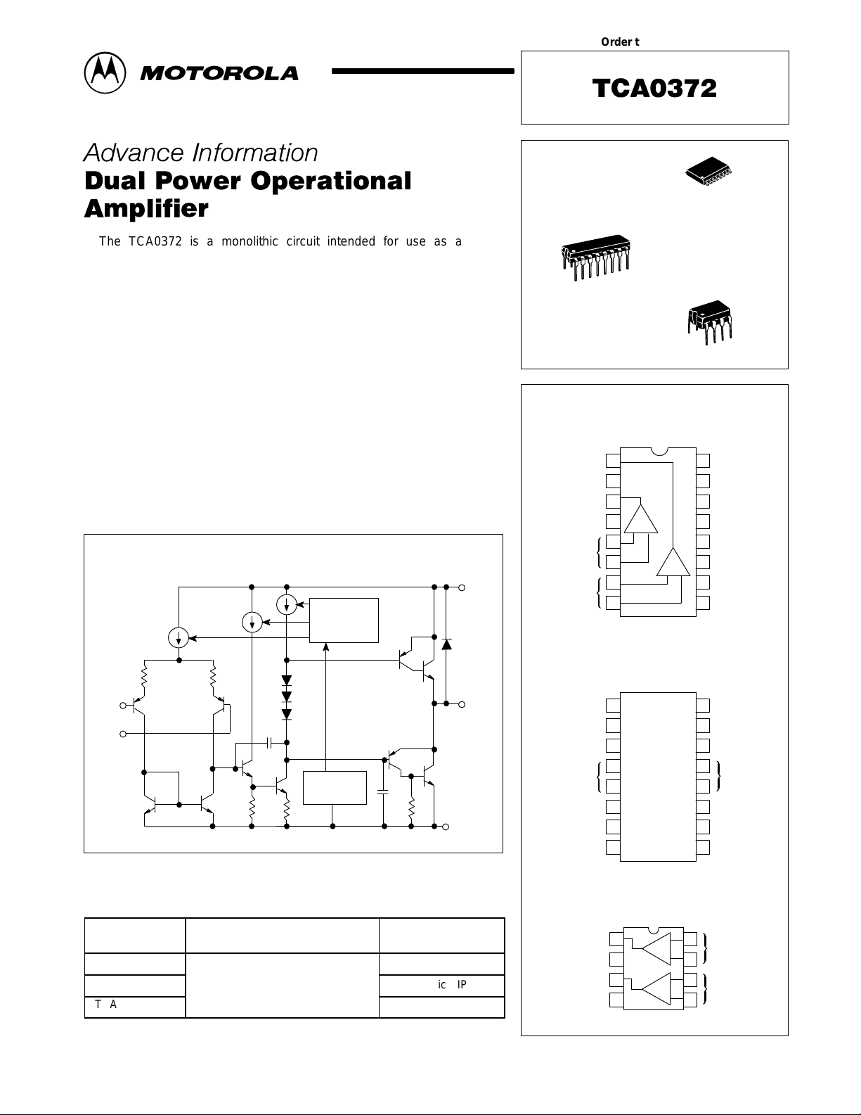
Representative Block Diagram
V
CC
Current
Bias
Monitoring
DW SUFFIX
PLASTIC PACKAGE
CASE 751G
SOP (12+2+2)L
16
1
DP1 SUFFIX
PLASTIC PACKAGE
CASE 626
16
1
DP2 SUFFIX
PLASTIC PACKAGE
CASE 648
8
1
PIN CONNECTIONS
TCA0372DP2
Output A
Output B
VEE/Gnd
Inputs B
Inputs A
1
2
V
CC
3
4
+
–
5
6
7
8
(Top View)
*Pins 4 and 9 to 16 are internally connected.
16
Gnd
15
Gnd
14
Gnd
13
Gnd
12
Gnd
11
+
Gnd
–
10
Gnd
9
Gnd
Inv.
Input
Output
Noninv.
Input
Thermal
Protection
V
EE
ORDERING INFORMATION
Operating
Device
TCA0372DW
TCA0372DP1
TCA0372DP2
This document contains information on a new product. Specifications and information herein
are subject to change without notice.
MOTOROLA ANALOG IC DEVICE DATA
Temperature Range
TJ = –40° to +150°C
Package
SOP (12+2+2) L
Plastic DIP
Plastic DIP
TCA0372DW
V
Output B
VEE/Gnd
Inputs –B
Inputs +B
CC
NC
NC
1
2
3
4
5
6
7
8
(Top View)
16
Output A
15
NC
14
NC
13
12
11
NC
10
Input –A
9
Input +A
VEE/Gnd
TCA0372DP1
Output A
Output B
VEE/Gnd
Motorola, Inc. 1996 Rev 1
1
2
V
CC
3
4
(Top View)
8
–
+
+
–
7
6
5
Inputs A
Inputs B
1
Page 2
MAXIMUM RATINGS
Rating Symbol Value Unit
Supply Voltage (from VCC to VEE) V
Input Differential Voltage Range V
Input Voltage Range V
Junction Temperature (Note 2) T
Storage Temperature Range T
DC Output Current I
Peak Output Current (Nonrepetitive) I
S
IDR
IR
J
stg
O
(max)
TCA0372
40 V
(Note 1) V
(Note 1) V
+150 °C
–55 to +150 °C
1.0 A
1.5 A
DC ELECTRICAL CHARACTERISTICS (V
Characteristics
Input Offset Voltage (VCM = 0)
TJ = +25°C
TJ, T
Average Temperature Coefficient of Of fset Voltage ∆VIO/∆T — 20 — µV/°C
Input Bias Current (VCM = 0) I
Input Offset Current (VCM = 0) I
Large Signal Voltage Gain
VO = ±10 V, RL = 2.0 k
Output Voltage Swing (IL = 100 mA)
TJ = +25°C
TJ = T
TJ = +25°C
TJ = T
Output Voltage Swing (IL = 1.0 A)
VCC = +24 V, VEE = 0 V, TJ = +25°C
VCC = +24 V, VEE = 0 V, TJ = T
VCC = +24 V, VEE = 0 V, TJ = +25°C
VCC = +24 V, VEE = 0 V, TJ = T
Input Common Mode Voltage Range
TJ = +25°C
TJ = T
Common Mode Rejection Ratio (RS = 10 k) CMRR 70 90 — dB
Power Supply Rejection Ratio (RS = 100 Ω) PSRR 70 90 — dB
Power Supply Current
TJ = +25°C
TJ = T
NOTES: 1. Either or both input voltages should not exceed the magnitude of VCC or VEE.
to T
low
high
to T
low
high
to T
low
high
to T
low
to T
low
to T
low
high
to T
low
high
2.Power dissipation must be considered to ensure maximum junction temperature (TJ) is not exceeded.
= +15 V, VEE = –15 V, RL connected to ground, TJ = –40° to +125°C.)
CC
Symbol Min Typ Max Unit
V
high
high
A
V
V
V
V
V
IO
IB
IO
VOL
OH
OL
OH
OL
ICR
I
D
—
—
— 100 500 nA
— 10 50 nA
30 100 — V/mV
14.0
13.9
—
—
22.5
22.5
—
—
VEE to (VCC –1.0)
VEE to (VCC –1.3)
—
—
1.0
—
14.2
—
–14.2
—
22.7
—
1.3
—
5.0
—
15
20
—
—
–14.0
–13.9
—
—
1.5
1.5
10
14
mV
V
V
V
mA
AC ELECTRICAL CHARACTERISTICS (V
Characteristics
Slew Rate (Vin = –10 V to +10 V, RL = 2.0 k, CL = 100 pF)
AV = –1.0, TJ = T
Gain Bandwidth Product (f = 100 kHz, CL = 100 pF, RL = 2.0 k)
TJ = 25°C
TJ = T
Phase Margin TJ = T
RL = 2.0 k, CL = 100 pF
Gain Margin
RL = 2.0 k, CL = 100 pF
Equivalent Input Noise Voltage
RS = 100 Ω, f = 1.0 to 100 kHz
Total Harmonic Distortion
AV = –1.0, RL = 50 Ω, VO = 0.5 VRMS, f = 1.0 kHz
NOTE: In case VEE is disconnected before VCC, a diode between VEE and Ground is recommended to avoid damaging the device.
low
to T
high
low
to T
low
high
to T
high
2
= +15 V, VEE = –15 V, RL connected to ground, TJ = +25°C, unless otherwise noted.)
CC
Symbol Min Typ Max Unit
SR 1.0 1.4 — V/µs
GBW
φ
m
A
m
e
n
THD — 0.02 — %
0.9
0.7
— 65 — Degrees
— 15 — dB
— 22 —
1.4
—
MOTOROLA ANALOG IC DEVICE DATA
—
MHz
—
nV/ Hz√
Page 3
TCA0372
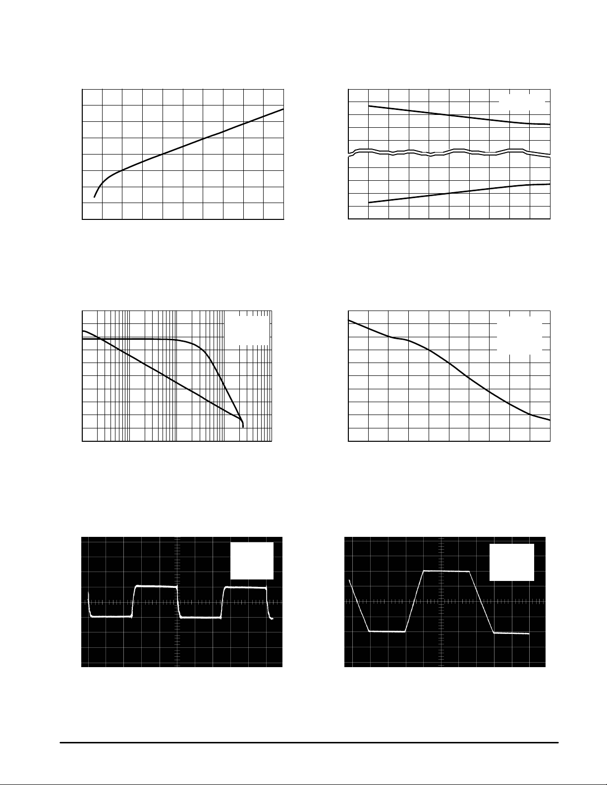
Figure 1. Supply Current versus Suppy V oltage
with No Load
6.5
5.5
4.5
, SUPPLY CURRENT (mA)I
3.5
CC
2.5
0 2.0 4.0 6.0 8.0 10 12 14 16 18 20
VCC, |VEE|, SUPPLY VOLTAGE (V)
Figure 3. V oltage Gain and Phase
versus Frequency
80
60
40
VCC = +15 V
VEE = –15 V
RL = 2.0 k
Figure 2. Output Saturation Voltage
versus Load Current
V
VCC–1.0
VCC–2.0
VCC+2.0
VCC+1.0
, OUTPUT SA TURATION VOLTAGE (V)V
sat
CC
V
EE
0 1.00.5
IL, LOAD CURRENT (A)
VCC = 24 V
VEE = 0 V
Figure 4. Phase Margin versus Output
Load Capacitance
80
90
Ω
100
70
60
50
VCC = +15 V
VEE = –15 V
Ω
RL = 2.0 k
AV = –100
GAIN (dB)
20
–20
1.0 10 100 1000 10000
f, FREQUENCY (kHz)
110
PHASE (DEGREES)
120
130
40
, PHASE MARGIN (DEGREES)
30
m
φ
20
0 0.8 1.2 1.6 2.0
0.4
CL, OUTPUT LOAD CAPACITANCE (nF)
Figure 5. Small Signal Transient Response Figure 6. Large Signal T ransient Response
VCC = +15 V
VEE = –15 V
AV = +1.0
Ω
RL = 2.0 k
,OUTPUT VOLTAGE (50 mV/DIV)
O
V
, OUTPUT VOLTAGE (5.0 V/DIV)
O
V
VCC = +15 V
VEE = –15 V
AV = +1.0
Ω
RL = 2.0 k
t, TIME (1.0 µs/DIV)
MOTOROLA ANALOG IC DEVICE DATA
t, TIME (10 µs/DIV)
3
Page 4

TCA0372
5.0 V/DIV200 mV/DIV
Figure 7. Sine Wave Reponse
t, TIME (100
µ
s/DIV)
Figure 9. Bidirectional Speed Control of DC Motors
R
x
V
R1
in
+
10 k
–
R2
10 k
VCC = +15 V
VEE = –15 V
AV = +100
RL = 50
R3
Ω
5.0
Ω
R5
10 k
0.1
Figure 8. Bidirectional DC Motor Control with
Microprocessor–Compatible Inputs
V
CC
+
VS/2
V
µ
F
0.1
µ
F
R6
10 k
–
VS = Logic Supply Voltage
Must Have VCC > V
E1, E2 = Logic Inputs
S
10 k
R7
+
–
10 k
R8
+
–
S
E2E1
For circuit stability, ensure that Rx > where, RM = internal resistance of motor.
The voltage available at the terminals of the motor is:
@
R1
where, |Ro| = and IM is the motor current.
2R3
R
x
2R3
THERMAL INFORMATION
The maximum power consumption an integrated circuit
can tolerate at a given operating ambient temperature can be
found from the equation:
P
=
D(T A)
where, P
= power dissipation allowable at a given
D(TA)
operating ambient temperature.
4
T
R
J(max)
(typ)
θJA
–T
A
@
R1
R
M
VM+
2(V1–
V
S
))|Ro|@I
2
M
This must be greater than the sum of the products of the
supply voltages and supply currents at the worst case
operating condition.
T
J(max)
= Maximum operating junction temperature
as listed in the maximum ratings section.
T
A
= Maximum desired operating ambient
temperature.
R
θJA(typ)
= Typical thermal resistance junction–to–
ambient.
MOTOROLA ANALOG IC DEVICE DATA
Page 5

–A–
16 9
D16X
M
0.010 (0.25) B
A
T
G14X
–B– P8X
81
S
S
C
K
TCA0372
OUTLINE DIMENSIONS
DW SUFFIX
PLASTIC PACKAGE
CASE 751G–02
(SOP (12+2+2)L)
ISSUE A
M
M
B
F
M
–T–
SEATING
PLANE
0.010 (0.25)
J
NOTES:
1. DIMENSIONING AND TOLERANCING PER ANSI
Y14.5M, 1982.
2. CONTROLLING DIMENSION: MILLIMETER.
3. DIMENSIONS A AND B DO NOT INCLUDE MOLD
PROTRUSION.
4. MAXIMUM MOLD PROTRUSION 0.15 (0.006) PER
SIDE.
5. DIMENSION D DOES NOT INCLUDE DAMBAR
PROTRUSION. ALLOWABLE DAMBAR
PROTRUSION SHALL BE 0.13 (0.005) TOTAL IN
EXCESS OF D DIMENSION AT MAXIMUM
MATERIAL CONDITION.
DIM MIN MAX MIN MAX
R
X 45
_
A 10.15 10.45 0.400 0.411
B 7.40 7.60 0.292 0.299
C 2.35 2.65 0.093 0.104
D 0.35 0.49 0.014 0.019
F 0.50 0.90 0.020 0.035
G 1.27 BSC 0.050 BSC
J 0.25 0.32 0.010 0.012
K 0.10 0.25 0.004 0.009
M 0 7 0 7
____
P 10.05 10.55 0.395 0.415
R 0.25 0.75 0.010 0.029
INCHESMILLIMETERS
DP2 SUFFIX
PLASTIC PACKAGE
CASE 648–08
ISSUE R
–A–
916
B
18
F
C
S
SEATING
–T–
PLANE
H
G
D
16 PL
0.25 (0.010) T
K
M
A
J
M
NOTES:
1. DIMENSIONING AND TOLERANCING PER ANSI
Y14.5M, 1982.
2. CONTROLLING DIMENSION: INCH.
3. DIMENSION L TO CENTER OF LEADS WHEN
FORMED PARALLEL.
4. DIMENSION B DOES NOT INCLUDE MOLD FLASH.
5. ROUNDED CORNERS OPTIONAL.
DIM MIN MAX MIN MAX
L
M
A 0.740 0.770 18.80 19.55
B 0.250 0.270 6.35 6.85
C 0.145 0.175 3.69 4.44
D 0.015 0.021 0.39 0.53
F 0.040 0.70 1.02 1.77
G 0.100 BSC 2.54 BSC
H 0.050 BSC 1.27 BSC
J 0.008 0.015 0.21 0.38
K 0.110 0.130 2.80 3.30
L 0.295 0.305 7.50 7.74
M 0 10 0 10
S 0.020 0.040 0.51 1.01
MILLIMETERSINCHES
____
MOTOROLA ANALOG IC DEVICE DATA
5
Page 6

NOTE 2
–T–
SEATING
PLANE
H
58
–B–
14
F
–A–
C
N
D
K
G
0.13 (0.005) B
M
T
TCA0372
OUTLINE DIMENSIONS
DP1 SUFFIX
PLASTIC PACKAGE
CASE 626–05
ISSUE K
L
J
M
M
A
M
NOTES:
1. DIMENSION L TO CENTER OF LEAD WHEN
FORMED PARALLEL.
2. PACKAGE CONTOUR OPTIONAL (ROUND OR
SQUARE CORNERS).
3. DIMENSIONING AND TOLERANCING PER ANSI
Y14.5M, 1982.
DIM MIN MAX MIN MAX
A 9.40 10.16 0.370 0.400
B 6.10 6.60 0.240 0.260
C 3.94 4.45 0.155 0.175
D 0.38 0.51 0.015 0.020
F 1.02 1.78 0.040 0.070
G 2.54 BSC 0.100 BSC
H 0.76 1.27 0.030 0.050
J 0.20 0.30 0.008 0.012
K 2.92 3.43 0.115 0.135
L 7.62 BSC 0.300 BSC
M ––– 10 ––– 10
N 0.76 1.01 0.030 0.040
INCHESMILLIMETERS
__
6
MOTOROLA ANALOG IC DEVICE DATA
Page 7

TCA0372
Motorola reserves the right to make changes without further notice to any products herein. Motorola makes no warranty , representation or guarantee regarding
the suitability of its products for any particular purpose, nor does Motorola assume any liability arising out of the application or use of any product or circuit, and
specifically disclaims any and all liability, including without limitation consequential or incidental damages. “T ypical” parameters which may be provided in Motorola
data sheets and/or specifications can and do vary in different applications and actual performance may vary over time. All operating parameters, including “Typicals”
must be validated for each customer application by customer’s technical experts. Motorola does not convey any license under its patent rights nor the rights of
others. Motorola products are not designed, intended, or authorized for use as components in systems intended for surgical implant into the body, or other
applications intended to support or sustain life, or for any other application in which the failure of the Motorola product could create a situation where personal injury
or death may occur. Should Buyer purchase or use Motorola products for any such unintended or unauthorized application, Buyer shall indemnify and hold Motorola
and its officers, employees, subsidiaries, affiliates, and distributors harmless against all claims, costs, damages, and expenses, and reasonable attorney fees
arising out of, directly or indirectly, any claim of personal injury or death associated with such unintended or unauthorized use, even if such claim alleges that
Motorola was negligent regarding the design or manufacture of the part. Motorola and are registered trademarks of Motorola, Inc. Motorola, Inc. is an Equal
Opportunity/Affirmative Action Employer.
MOTOROLA ANALOG IC DEVICE DATA
7
Page 8

TCA0372
How to reach us:
USA/EUROPE / Locations Not Listed: Motorola Literature Distribution; JAPAN: Nippon Motorola Ltd.; Tatsumi–SPD–JLDC, 6F Seibu–Butsuryu–Center,
P.O. Box 20912; Phoenix, Arizona 85036. 1–800–441–2447 or 602–303–5454 3–14–2 Tatsumi Koto–Ku, Tokyo 135, Japan. 03–81–3521–8315
MFAX: RMF AX0@email.sps.mot.com – TOUCHT ONE 602–244–6609 ASIA/PACIFIC: Motorola Semiconductors H.K. Ltd.; 8B Tai Ping Industrial Park,
INTERNET: http://Design–NET.com 51 Ting Kok Road, Tai Po, N.T., Hong Kong. 852–26629298
8
◊
MOTOROLA ANALOG IC DEVICE DATA
TCA0372/D
*TCA0372/D*
 Loading...