

Page 1
CSD-EL300
US
SERVICE MANUAL
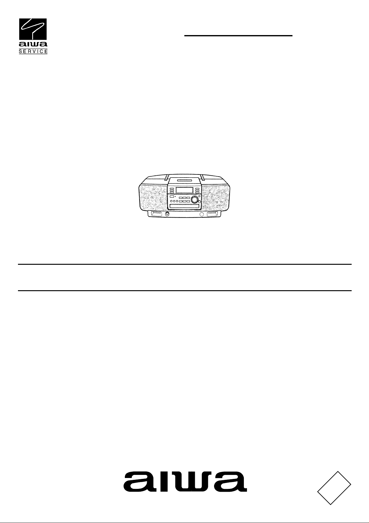
COMPACT DISC STEREO RADIO
CASSETTE RECORDER
BASIC TAPE MECHANISM : 2ZM-1YR7NC
BASIC CD MECHANISM : 3ZG-3 E2NC
S/M Code No. 09-003-344-1N1
DATA
Page 2
SPECIFICATIONS
Design and specifications are subject to change without
•
notice
.
ACCESSORIES/PACKAGE LIST
REF. NO PART NO. KANRI DESCRIPTION
1 8A-CH2-903-010 IB,U(ESF)FM
2 8A-CH2-950-010 RC UNIT,ACH-2
!
3 87-A80-027-010 AC CORD SET,U BLK SPT2
NO.
2
Page 3
PROTECTION OF EYES FROM LASER BEAM DURING SERVICING
This set employs laser. Therefore, be sure to follow carefully the
instructions below when servicing.
WARNING!
WHEN SERVICING, DO NOT APPROACH THE LASER EXIT
WITH THE EYE TOO CLOSELY. IN CASE IT IS NECESSARY TO
CONFIRM LASER BEAM EMISSION. BE SURE TO OBSERVE
FROM A DISTANCE OF MORE THAN 30cm FROM THE
SURFACE OF THE OBJECTIVE LENS ON THE OPTICAL
PICK-UP BLOCK.
Caution: Invisible laser radiation when
open and interlocks defeated avoid exposure to beam.
Advarsel:Usynling laserståling ved åbning,
når sikkerhedsafbrydere er ude af funktion.
Undgå udsættelse for stråling.
VAROITUS!
Laiteen Käyttäminen muulla kuin tässä käyttöohjeessa mainitulla tavalla saattaa altistaa käyt-täjän turvallisuusluokan 1 ylittävälle näkymättömälle lasersäteilylle.
VARNING!
Om apparaten används på annat sätt än vad som specificeras i
denna bruksanvising, kan användaren utsättas för osynling
laserstrålning, som överskrider gränsen för laserklass 1.
CAUTION
Use of controls or adjustments or performance of procedures
other than those specified herein may result in hazardous
radiation exposure.
ATTENTION
L'utilisation de commandes, réglages ou procédures autres que
ceux spécifiés peut entraîner une dangereuse exposition aux
radiations.
ADVARSEL!
Usynlig laserståling ved åbning, når sikkerhedsafbrydereer ude
af funktion. Undgå udsættelse for stråling.
This Compact Disc player is classified as a CLASS 1 LASER
product.
The CLASS 1 LASER PRODUCT label is located on the rear
exterior.
CLASS 1
KLASSE 1
LUOKAN 1
KLASS 1
LASER PRODUCT
LASER PRODUKT
LASER LAITE
LASER APPARAT
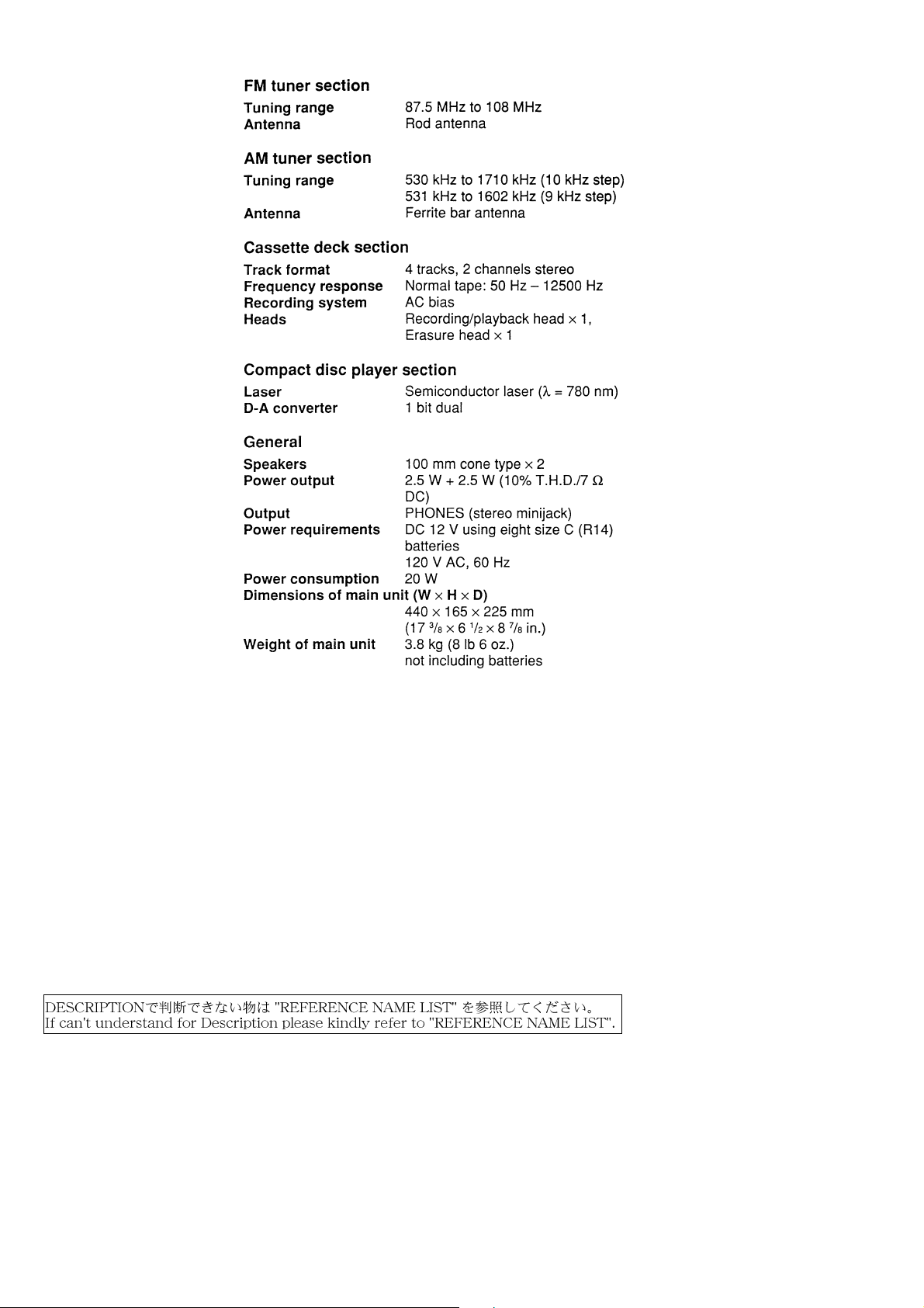
Precaution to replace Optical block
(KSS-213F)
Body or clothes electrostatic potential could ruin
laser diode in the optical block. Be sure ground
body and workbench, and use care the clothes
do not touch the diode.
1) After the connection, remove solder shown in
the right figure.
3
Page 4

ELECTRICAL MAIN PARTS LIST
REF. NO PART NO. KANRI DESCRIPTION
IC
87-A21-550-010 IC,TA2149N
87-A21-185-040 C-IC,LC72121M
87-A21-090-010 IC,LA4600
87-A21-416-040 C-IC,M61500FP
87-A21-607-010 IC,NJM14558LD
87-017-915-080 IC,BU4094BCF
87-A20-446-010 C-IC,LA9241ML
87-A20-187-010 IC,LC78622E
87-A21-093-010 IC,LA6541D
8A-CH2-612-010 C-IC,LC867132-5P07
87-A20-911-010 IC,RPM6938
87-001-982-010 IC,TA7291S
TRANSISTOR
89-327-143-080 TR,2SC2714 (0.1W)
87-026-447-080 TR,2SC1740S R
89-111-624-080 TR,2SA1162Y
87-026-213-080 CHIP-TR,DTC114YK
89-327-125-080 CHIP TR,2SC2712GR
87-A30-090-080 FET,2SK2541
87-A30-151-080 TR,2SA1993F
87-026-610-080 TR,KTC3198GR
87-A30-190-080 TR,CC5551
87-026-502-080 DTC144TS
87-A30-154-080 TR,RT1N441S
87-026-463-080 TR,2SA933S (0.3W)
89-109-332-380 TR,2SA933RS
89-113-184-080 TR,2SA1318T
87-026-464-080 TR,DTC114TS (0.3W)
87-026-218-080 TR,DTC144ES (0.2W)
89-318-155-080 TR,2SC1815 (0.4W)
89-112-965-080 TR,2SA1296 (0.75W)
87-026-291-080 TR,DTC124XS
89-318-154-080 TR,2SC1815 (0.4W)
89-213-702-010 TR,2SB1370 (1.8W)
87-026-462-080 TR,2SC1740 S(RS 0.3W)
87-026-237-080 CHIP-TR,DTC124XK
87-A30-075-080 C-TR,2SA1235F
87-026-235-080 CHIP-TR,DTC114EK
87-026-245-080 TR,DTC114ES
89-109-521-080 TR,2SA952 (0.6W)
DIODE
87-070-345-080 DIODE,IN4148
87-A40-616-070 VARI-CAP,SVC384(S/T)
87-A40-128-080 C-VARI-CAP,HVU202A
87-017-072-080 ZENER,HZS3B1
87-020-465-080 DIODE,1SS133 (110MA)
87-020-465-010 DIODE,1SS133 (110MA)
87-001-936-080 ZENER,HZS7A3L
87-017-149-080 ZENER,HZS6A2L
87-017-161-080 ZENER,HZS7C2L
87-017-148-080 ZENER,HZS6A1L
87-017-144-080 ZENER,HZS24 2
87-001-142-080 DIODE,1SS294 (100MA)
87-020-125-080 DIODE,1SS181 (100MA)
87-020-027-080 CHIP-DIODE 1SS184
87-A40-465-090 DIODE,FR202
MAIN C.B
C211 87-010-405-080 CAP, ELECT 10-50V
C212 87-010-405-080 CAP, ELECT 10-50V
C220 87-010-406-080 CAP, ELECT 22-50
C229 87-018-125-080 CAP, CER 330P-50V
C230 87-018-134-080 CAPACITOR,TC-U 0.01-16
NO.
REF. NO PART NO. KANRI DESCRIPTION
C233 87-010-546-080 CAP, ELECT 0.33-50V
C234 87-010-546-080 CAP, ELECT 0.33-50V
C235 87-018-209-080 CAP, CER 0.1-50V
C236 87-018-209-080 CAP, CER 0.1-50V
C237 87-010-370-080 CAP, ELECT 330-6.3V
C238 87-010-263-080 CAP, ELECT 100-10V
C239 87-018-134-080 CAPACITOR,TC-U 0.01-16
C240 87-018-134-080 CAPACITOR,TC-U 0.01-16
C241 87-010-401-080 CAP, ELECT 1-50V
C242 87-010-401-080 CAP, ELECT 1-50V
C243 87-010-401-080 CAP, ELECT 1-50V
C244 87-010-401-080 CAP, ELECT 1-50V
C245 87-010-401-080 CAP, ELECT 1-50V
C246 87-010-401-080 CAP, ELECT 1-50V
C263 87-018-131-080 CAP, CER 1000P-50V
C264 87-018-131-080 CAP, CER 1000P-50V
C265 87-010-545-080 CAP, ELECT 0.22-50V
C266 87-010-545-080 CAP, ELECT 0.22-50V
C271 87-010-221-080 CAP, ELECT 470-10V
C272 87-010-221-080 CAP, ELECT 470-10V
C277 87-010-404-080 CAP, ELECT 4.7-50V
C278 87-010-263-080 CAP, ELECT 100-10V
C279 87-010-263-080 CAP, ELECT 100-10V
C287 87-018-130-080 CAP,TC-U 820P-50 B
C288 87-018-130-080 CAP,TC-U 820P-50 B
C301 87-018-131-080 CAP, CER 1000P-50V
C302 87-018-131-080 CAP, CER 1000P-50V
C305 87-010-263-080 CAP, ELECT 100-10V
C306 87-010-263-080 CAP, ELECT 100-10V
C307 87-018-203-080 CAP, CER 8200P-16V
C308 87-018-203-080 CAP, CER 8200P-16V
C311 87-010-546-080 CAP, ELECT 0.33-50V
C312 87-010-546-080 CAP, ELECT 0.33-50V
C313 87-018-201-080 CAP,TC-U 5600P-16 X
C314 87-018-201-080 CAP,TC-U 5600P-16 X
C321 87-018-205-080 CAP, CERA-SOL 0.022
C323 87-018-041-080 CAP,TC-S 560P-50 B
C324 87-018-041-080 CAP,TC-S 560P-50 B
C331 87-018-126-080 CAP,TC-U 390P-50 B
C332 87-018-126-080 CAP,TC-U 390P-50 B
C333 87-018-128-080 CAP, CERA-SOL SS 560P
C334 87-018-131-080 CAP, CER 1000P-50V
C335 87-018-201-080 CAP,TC-U 5600P-16 X
C336 87-018-134-080 CAPACITOR,TC-U 0.01-16
C337 87-018-198-080 CAP,TC-U 2700P-16 X
C338 87-018-198-080 CAP,TC-U 2700P-16 X
C339 87-018-198-080 CAP,TC-U 2700P-16 X
C340 87-010-382-080 CAP, ELECT 22-25V
C341 87-018-205-080 CAP, CERA-SOL 0.022
C342 87-018-123-080 CAP, CER 220P-50V
C343 87-018-199-080 CAP, CER 3300P
C345 87-018-131-080 CAP, CER 1000P-50V
C346 87-018-131-080 CAP, CER 1000P-50V
C347 87-010-374-080 CAP, ELECT 47-10V
C348 87-018-131-080 CAP, CER 1000P-50V
C355 87-A11-131-080 CAP,TC U 8200P-50 K B
C356 87-A11-131-080 CAP,TC U 8200P-50 K B
C363 87-010-405-080 CAP, ELECT 10-50V
C364 87-010-405-080 CAP, ELECT 10-50V
C367 87-018-043-080 CAP,TC-S 820P-50 B
C368 87-018-043-080 CAP,TC-S 820P-50 B
C369 87-018-118-080 CAP,TC-U 82P-50 B
C370 87-018-118-080 CAP,TC-U 82P-50 B
C373 87-010-401-080 CAP, ELECT 1-50V
C374 87-010-401-080 CAP, ELECT 1-50V
C382 87-010-401-080 CAP, ELECT 1-50V
C383 87-010-248-080 CAP, ELECT 220-10V
C384 87-010-374-080 CAP, ELECT 47-10V
C387 87-018-123-080 CAP, CER 220P-50V
C511 87-010-263-080 CAP, ELECT 100-10V
NO.
4
Page 5

REF. NO PART NO. KANRI DESCRIPTION
C513 87-018-134-080 CAPACITOR,TC-U 0.01-16
C514 87-010-248-080 CAP, ELECT 220-10V
C520 87-010-384-080 CAP, ELECT 100-25V
C521 87-016-495-000 CAP,E 3300-25 M SMG
C526 87-010-404-080 CAP, ELECT 4.7-50V
C527 87-010-401-080 CAP, ELECT 1-50V
C528 87-010-221-080 CAP, ELECT 470-10V
C529 87-010-263-080 CAP, ELECT 100-10V
C530 87-010-248-080 CAP, ELECT 220-10V
C531 87-010-265-080 CAP, ELECT 33-16V
C536 87-010-263-080 CAP, ELECT 100-10V
C543 87-010-401-080 CAP, ELECT 1-50V
CN201 87-A60-054-010 CONN,14P V 9604S-14C
CN202 87-A60-058-010 CONN,10P V 9604S-10C
CN203 87-049-469-010 CONN,4P V
CN301 87-A60-112-010 CONN,7P V S2M-7W
CN501 87-099-827-010 CONN,3P S2M-3W
CNA1 8A-CH2-631-010 CONN ASSY,6P TU-AF
J201 87-009-216-010 JACK, DIA 3.5
L301 87-003-131-080 COIL, 10MH
L331 87-007-342-010 COIL,OSC 85K BIAS
CD MAIN C.B
C401 87-010-403-080 CAP, ELECT 3.3-50V
C402 87-018-134-080 CAPACITOR,TC-U 0.01-16
C403 87-010-263-080 CAP, ELECT 100-10V
C404 87-010-248-080 CAP, ELECT 220-10V
C405 87-018-134-080 CAPACITOR,TC-U 0.01-16
C406 87-010-374-080 CAP, ELECT 47-10V
C407 87-018-131-080 CAP, CER 1000P-50V
C409 87-010-248-080 CAP, ELECT 220-10V
C410 87-010-263-080 CAP, ELECT 100-10V
C412 87-010-401-080 CAP, ELECT 1-50V
C414 87-010-405-080 CAP, ELECT 10-50V
C416 87-010-545-080 CAP, ELECT 0.22-50V
C417 87-018-125-080 CAP, CER 330P-50V
C425 87-018-129-080 CAP, CER 680P-50V
C429 87-018-133-080 CAPACITOR,CER 4700P-16V
C430 87-018-123-080 CAP, CER 220P-50V
C431 87-010-545-080 CAP, ELECT 0.22-50V
C432 87-010-374-080 CAP, ELECT 47-10V
C433 87-010-401-080 CAP, ELECT 1-50V
C434 87-018-199-080 CAP, CER 3300P
C435 87-018-134-080 CAPACITOR,TC-U 0.01-16
C436 87-010-374-080 CAP, ELECT 47-10V
C437 87-010-404-080 CAP, ELECT 4.7-50V
C438 87-018-209-080 CAP, CER 0.1-50V
C439 87-018-131-080 CAP, CER 1000P-50V
C440 87-018-139-080 CAP,TC-U 1P-50 CH
C442 87-018-149-080 CAP,TC-U 15P-50 CH
C443 87-018-209-080 CAP, CER 0.1-50V
C444 87-018-134-080 CAPACITOR,TC-U 0.01-16
C445 87-018-209-080 CAP, CER 0.1-50V
C446 87-018-209-080 CAP, CER 0.1-50V
C447 87-018-209-080 CAP, CER 0.1-50V
C448 87-018-111-080 CAP, CERA-SOL SS 27P
C450 87-018-127-080 CAP, CER 470P-50V
C451 87-018-123-080 CAP, CER 220P-50V
C455 87-010-263-080 CAP, ELECT 100-10V
C457 87-018-113-080 CAP, CER 33P-50V
C458 87-018-113-080 CAP, CER 33P-50V
C459 87-010-263-080 CAP, ELECT 100-10V
C460 87-018-209-080 CAP, CER 0.1-50V
C461 87-018-209-080 CAP, CER 0.1-50V
C462 87-010-248-080 CAP, ELECT 220-10V
C463 87-018-134-080 CAPACITOR,TC-U 0.01-16
C465 87-010-404-080 CAP, ELECT 4.7-50V
C466 87-018-209-080 CAP, CER 0.1-50V
NO.
REF. NO PART NO. KANRI DESCRIPTION
C467 87-010-263-080 CAP, ELECT 100-10V
C468 87-018-119-080 CAP, CER 100P-50V
C469 87-018-121-080 CAP, CER 150P-50V
C470 87-010-544-080 CAP, ELECT 0.1-50V
C471 87-A11-144-080 CAPACITOR,TC-U 0.1-16
C472 87-A11-144-080 CAPACITOR,TC-U 0.1-16
C473 87-A11-144-080 CAPACITOR,TC-U 0.1-16
C474 87-A11-144-080 CAPACITOR,TC-U 0.1-16
C475 87-018-134-080 CAPACITOR,TC-U 0.01-16
C476 87-010-236-080 CAP,E 1000-10 SME
C477 87-018-134-080 CAPACITOR,TC-U 0.01-16
C478 87-010-263-080 CAP, ELECT 100-10V
C479 87-018-134-080 CAPACITOR,TC-U 0.01-16
C480 87-010-221-080 CAP, ELECT 470-10V
C481 87-010-405-080 CAP, ELECT 10-50V
C482 87-010-405-080 CAP, ELECT 10-50V
C483 87-018-123-080 CAP, CER 220P-50V
C484 87-018-123-080 CAP, CER 220P-50V
C487 87-018-134-080 CAPACITOR,TC-U 0.01-16
C489 87-018-209-080 CAP, CER 0.1-50V
C490 87-018-209-080 CAP, CER 0.1-50V
C491 87-018-134-080 CAPACITOR,TC-U 0.01-16
C492 87-010-221-080 CAP, ELECT 470-10V
C493 87-018-197-080 CAP, CER 1800P-50V
C494 87-010-405-080 CAP, ELECT 10-50V
C501 87-018-119-080 CAP, CER 100P-50V
C502 87-018-119-080 CAP, CER 100P-50V
C503 87-018-119-080 CAP, CER 100P-50V
C504 87-018-119-080 CAP, CER 100P-50V
C505 87-018-119-080 CAP, CER 100P-50V
C506 87-018-119-080 CAP, CER 100P-50V
C901 87-018-134-080 CAPACITOR,TC-U 0.01-16
C902 87-010-263-080 CAP, ELECT 100-10V
C903 87-018-209-080 CAP, CER 0.1-50V
CN401 87-A60-424-010 CONN,16P V TOC-B
CN402 87-A60-061-010 CONN,06P V 9604S-06C
CN403 87-A60-062-010 CONN,05P V 9604S-05C
X401 81-592-641-010 VIB,CER 16.93MHZ
TU C.B
C1 87-010-314-080 C-CAP,S 22P-50V
C2 87-010-316-080 C-CAP,S 33P-50 CH
C3 87-010-314-080 C-CAP,S 22P-50V
C5 87-016-669-080 C-CAP,S 0.1-25 K B
C6 87-010-313-080 CAP, CHIP 18P
C7 87-014-049-080 CAP,PP 470P-100 J
C8 87-012-349-080 C-CAP,S 1000P-50 CH
C10 87-010-197-080 CAP, CHIP 0.01 DM
C11 87-010-197-080 CAP, CHIP 0.01 DM
C12 87-010-197-080 CAP, CHIP 0.01 DM
C13 87-010-150-080 C-CAP,S 6P-50 CH
C14 87-010-303-080 C-CAP,S 330P-50CH
C15 87-010-178-080 CHIP CAP 1000P
C16 87-010-374-080 CAP, ELECT 47-10V
C17 87-010-198-080 CAP, CHIP 0.022
C18 87-015-835-080 C-CAP,0.047 D
C19 87-010-263-080 CAP, ELECT 100-10V
C20 87-010-404-080 CAP, ELECT 4.7-50V
C21 87-010-197-080 CAP, CHIP 0.01 DM
C22 87-010-197-080 CAP, CHIP 0.01 DM
C23 87-010-197-080 CAP, CHIP 0.01 DM
C24 87-010-303-080 C-CAP,S 330P-50CH
C25 87-016-460-080 C-CAP,S 0.22-16 B
C27 87-A11-067-080 C-CAP,S 1-10 K B
C28 87-016-669-080 C-CAP,S 0.1-25 K B
C29 87-016-669-080 C-CAP,S 0.1-25 K B
C30 87-010-365-080 CAP, CHIP 0.027
C31 87-010-365-080 CAP, CHIP 0.027
C33 87-012-358-080 C-CAP,S 0.47-10 F Z
NO.
5
Page 6

REF. NO PART NO. KANRI DESCRIPTION
C34 87-012-358-080 C-CAP,S 0.47-10 F Z
C35 87-015-819-080 CAPACITOR,0.01
C36 87-010-263-080 CAP, ELECT 100-10V
C37 87-010-197-080 CAP, CHIP 0.01 DM
C38 87-010-374-080 CAP, ELECT 47-10V
C39 87-010-404-080 CAP, ELECT 4.7-50V
C40 87-010-197-080 CAP, CHIP 0.01 DM
C41 87-010-178-080 CHIP CAP 1000P
C42 87-010-178-080 CHIP CAP 1000P
C43 87-010-178-080 CHIP CAP 1000P
C44 87-010-311-080 CAP 12P
C45 87-010-312-080 C-CAP,S 15P-50 CH
C46 87-010-197-080 CAP, CHIP 0.01 DM
C47 87-010-197-080 CAP, CHIP 0.01 DM
C48 87-010-197-080 CAP, CHIP 0.01 DM
C49 87-012-140-080 CAP 470P
C50 87-010-197-080 CAP, CHIP 0.01 DM
C71 87-010-197-080 CAP, CHIP 0.01 DM
C72 87-010-263-080 CAP, ELECT 100-10V
C73 87-010-197-080 CAP, CHIP 0.01 DM
C75 87-010-197-080 CAP, CHIP 0.01 DM
C91 87-012-140-080 CAP 470P
C92 87-010-197-080 CAP, CHIP 0.01 DM
C93 87-010-197-080 CAP, CHIP 0.01 DM
CF1 87-A91-094-010 FLTR,CDA10.7 MG80A
CF2 87-008-261-010 FILTER, SFE10.7MA5-A
CF3 87-008-261-010 FILTER, SFE10.7MA5-A
CN2 87-099-854-010 CONN,6P S2M-6W
CN3 87-A60-110-010 CONN,4P V S2M-4W
HD1 88-CD6-661-010 HLDR,BAR ANT.
HD2 88-CD6-661-010 HLDR,BAR ANT.
L2 87-A50-560-010 COIL,FM BPF(ACD)
L3 8A-CH4-670-010 BAR-ANT,MW 2B-ACH(COI)
L4 87-A50-420-010 COIL,MW OSC(SYN)
L5 87-A50-566-010 COIL,FM RF EX(ACH)
L6 87-A50-567-010 COIL,FM OSC(ACH)
L7 87-A91-308-010 FLTR,PCFAZH- 450T (TOK)
L8 87-005-849-080 COIL,10UH(CECS)
TC1 87-011-254-080 TRIMER,20P LAR
X1 87-A70-061-010 VIB,XTAL 4.500MHZ CSA-309
FRONT C.B
C601 87-010-263-080 CAP, ELECT 100-10V
C601 87-010-555-040 CAP,E 100-10 GAS
C602 87-010-197-080 CAP, CHIP 0.01 DM
C603 87-015-696-080 CAP,E 2.2-50 7L
C603 87-010-495-040 CAP,E 2.2-50 GAS
C604 87-010-754-080 CAP,E220-10 SRA 7L
C605 87-010-196-080 CHIP CAPACITOR,0.1-25
C606 87-015-696-080 CAP,E 2.2-50 7L
C606 87-010-495-040 CAP,E 2.2-50 GAS
C607 87-015-694-080 CAP,E 0.47-50 7L
C607 87-010-493-040 CAP,E 0.47-50 GAS
C608 87-010-196-080 CHIP CAPACITOR,0.1-25
C609 87-010-313-080 CAP, CHIP 18P
C610 87-010-314-080 C-CAP,S 22P-50V
C611 87-010-317-080 C-CAP,S 39P-50 CH
C612 87-010-317-080 C-CAP,S 39P-50 CH
C613 87-010-312-080 C-CAP,S 15P-50 CH
C614 87-010-754-080 CAP,E220-10 SRA 7L
C616 87-010-322-080 C-CAP,S 100P-50 CH
C617 87-010-322-080 C-CAP,S 100P-50 CH
C618 87-010-197-080 CAP, CHIP 0.01 DM
C619 87-010-197-080 CAP, CHIP 0.01 DM
C620 87-018-044-080 CAP,TC-S 1000P-50 B
C620 87-010-178-080 CHIP CAP 1000P
C621 87-010-405-080 CAP, ELECT 10-50V
NO.
REF. NO PART NO. KANRI DESCRIPTION
C622 87-012-154-080 C-CAP,S 150P-50 CH
C623 87-012-154-080 C-CAP,S 150P-50 CH
C625 87-010-322-080 C-CAP,S 100P-50 CH
C626 87-010-197-080 CAP, CHIP 0.01 DM
C627 87-010-196-080 CHIP CAPACITOR,0.1-25
C628 87-015-677-080 CAP,E 100-6.3 7L
C628 87-015-819-080 CAPACITOR,0.01
C629 87-010-318-080 C-CAP,S 47P-50 CH
C630 87-010-178-080 CHIP CAP 1000P
C631 87-010-322-080 C-CAP,S 100P-50 CH
C632 87-010-318-080 C-CAP,S 47P-50 CH
C633 87-010-322-080 C-CAP,S 100P-50 CH
C634 87-015-677-080 CAP,E 100-6.3 7L
C635 87-010-197-080 CAP, CHIP 0.01 DM
CN601 87-099-203-010 CONN,10P 6216 H
CN602 87-099-031-010 CONN,14P 6216 H
CNA602 8A-CH2-625-010 CONN ASSY,9P TA-ME
D601 87-A40-162-010 LED,L-1154SRD
L601 87-003-171-010 COIL,15UH TROIDAL
LCD601 8A-CH2-611-010 LCD,AIW4213
!
R668 87-029-124-010 RES,FUSE 2.2-1/4
S381 87-A91-636-010 SW,RTRY 1-2-24 EVEGA1F2024B
SW601 87-A90-095-080 SW,TACT EVQ11G04M
SW602 87-A90-095-080 SW,TACT EVQ11G04M
SW603 87-A90-095-080 SW,TACT EVQ11G04M
SW604 87-A90-095-080 SW,TACT EVQ11G04M
SW605 87-A90-095-080 SW,TACT EVQ11G04M
SW606 87-A90-095-080 SW,TACT EVQ11G04M
SW607 87-A90-095-080 SW,TACT EVQ11G04M
SW608 87-A90-095-080 SW,TACT EVQ11G04M
SW609 87-A90-095-080 SW,TACT EVQ11G04M
SW610 87-A90-095-080 SW,TACT EVQ11G04M
SW612 87-A90-095-080 SW,TACT EVQ11G04M
SW613 87-A90-095-080 SW,TACT EVQ11G04M
SW614 87-A90-095-080 SW,TACT EVQ11G04M
SW615 87-A90-095-080 SW,TACT EVQ11G04M
SW616 87-A90-095-080 SW,TACT EVQ11G04M
SW617 87-A90-095-080 SW,TACT EVQ11G04M
SW618 87-A90-095-080 SW,TACT EVQ11G04M
SW619 87-A90-095-080 SW,TACT EVQ11G04M
X601 87-030-273-010 VIB,XTAL 32.768K5PPM
X602 87-A70-070-080 VIB,CER 5.76MHZ CRHF
PWR C.B
C701 87-018-205-080 CAP, CERA-SOL 0.022
C702 87-018-205-080 CAP, CERA-SOL 0.022
C703 87-018-205-080 CAP, CERA-SOL 0.022
C704 87-018-205-080 CAP, CERA-SOL 0.022
FC701 87-A90-160-080 FUSE CLAMP,FC 51F
FC702 87-A90-160-080 FUSE CLAMP,FC 51F
LED C.B
CNA601 8A-CH2-624-010 CONN ASSY,4P FR-TU
D651 87-A40-161-010 LED,L-1154SGD
D652 87-A40-161-010 LED,L-1154SGD
D653 87-A40-161-010 LED,L-1154SGD
D654 87-A40-161-010 LED,L-1154SGD
D655 87-A40-161-010 LED,L-1154SGD
D656 87-A40-161-010 LED,L-1154SGD
D657 87-A40-161-010 LED,L-1154SGD
D658 87-A40-161-010 LED,L-1154SGD
D659 87-A40-161-010 LED,L-1154SGD
D660 87-A40-161-010 LED,L-1154SGD
NO.
6
Page 7
REF. NO PART NO. KANRI DESCRIPTION
MOTOR C.B
CON1 87-099-210-010 CONN,5P 6216 H
M1 87-045-305-010 MOTOR,RF-500TB DC-5V (2MA)
SW1 87-036-110-010 PUSH SWITCH
SW2 87-036-110-010 PUSH SWITCH
BATT2 C.B
• Regarding connectors, they are not stocked as they are not the initial order items.
The connectors are available after they are supplied from connector manufacturers upon the order is received.
NO.
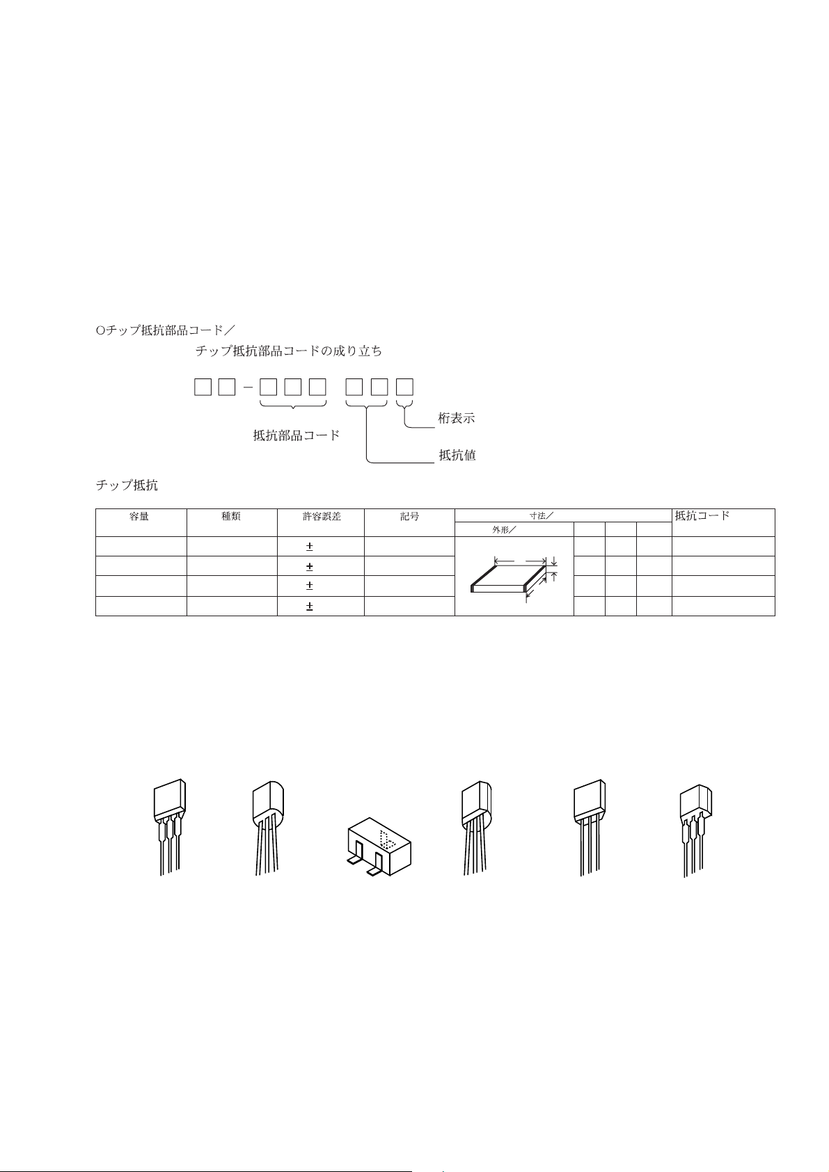
CHIP RESISTOR PART CODE
Chip Resistor Part Coding
88
A
Resistor Code
Chip resistor
Wattage Type Tolerance
1/16W 1005 5% CJ
1/16W
1/10W
1/8W
1608
2125
3216
5%
5%
5%
TRANSISTOR ILLUSTRATION
Symbol
CJ
CJ
CJ
C
Figure
Value of resistor
Form
L
Dimensions (mm)
t
W
0.55
Resistor Code
108
118
128
LW t
1.0 0.5 0.35 104
1.6 0.8 0.45
2 1.25 0.45
3.2
1.6
: A
: A
ECB ECB
2SA952
2SA1296
2SA1318
2SA1993
2SC1740
2SC1815
CC5551
KTC3198
E
2SA1162
2SA1235
2SC2712
2SC2714
DTC114YK
DTC124XK
DTC144EK
RT1N441S
DTC124XS2SA933
7
B
ECB ECBECB
2SK2541
DTC114ES
DTC114TS
Page 8
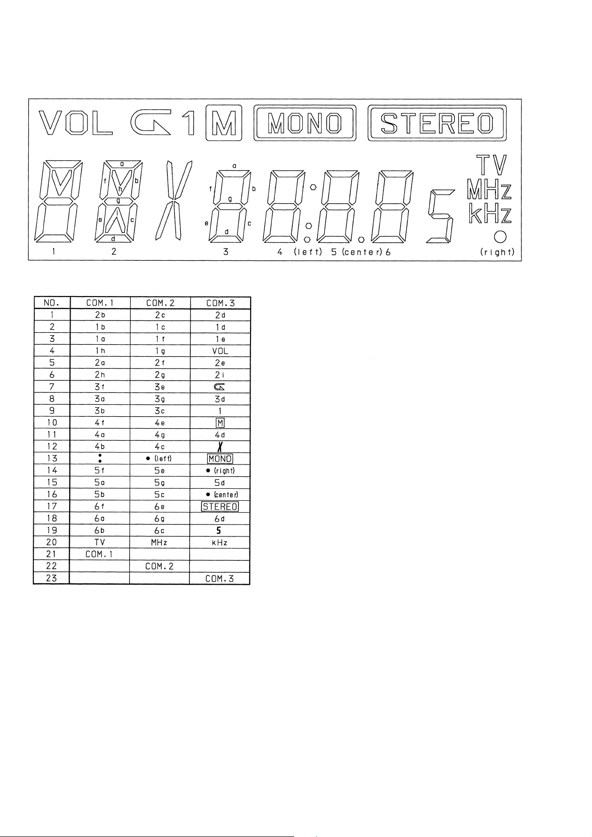
LCD DISPLAY
LCD, AIW4213
8
Page 9
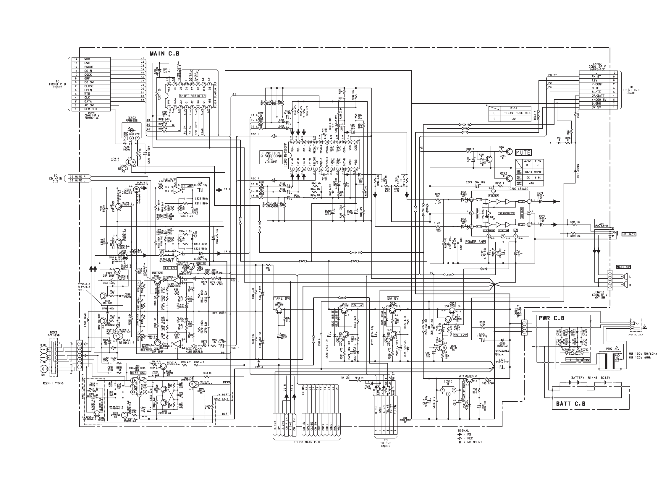
SCHEMATIC DIAGRAM-1 (MAIN)
109
Page 10
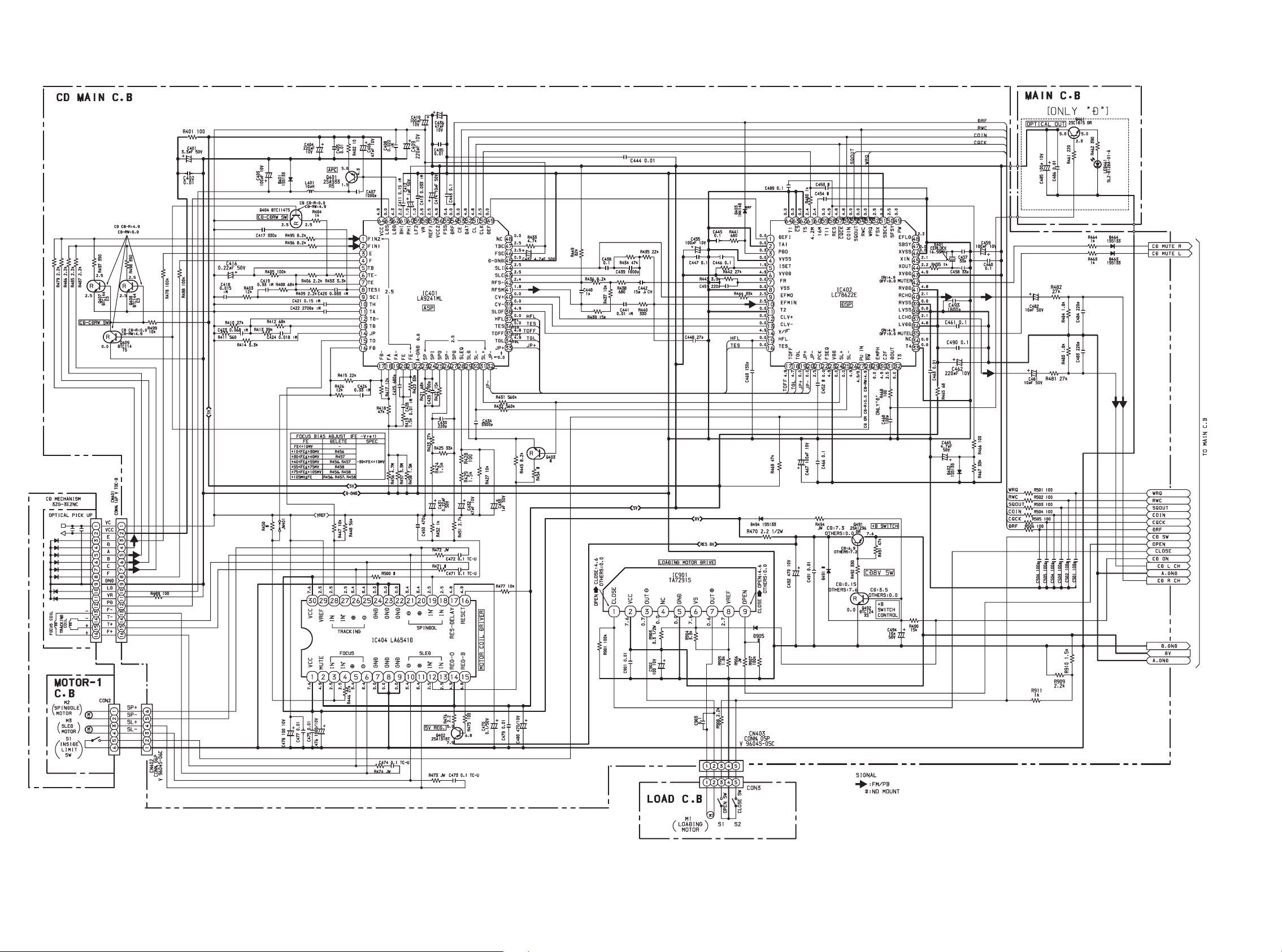
SCHEMATIC DIAGRAM-2 (CD MAIN)
1211
Page 11
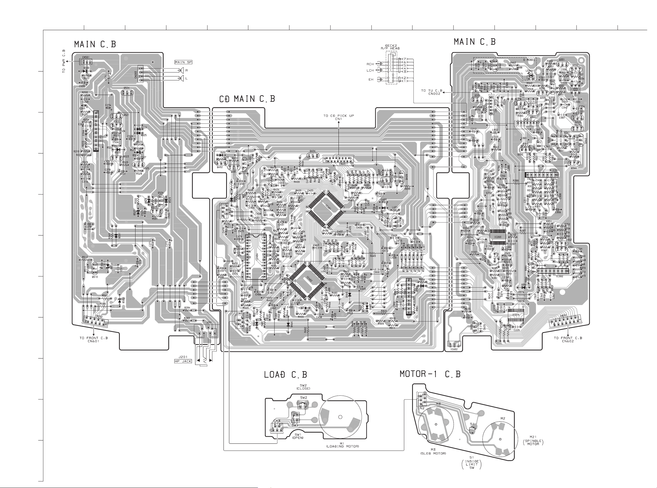
WIRING-1 (MAIN/CD MAIN)
1
A
B
C
D
234567
8
9
10
11 12 13
14
E
F
G
H
I
J
K
1413
Page 12

WIRING-2 (PWR/BATT)
1
234567
WIRING-3 (TU)
1
234567
A
B
C
F705
D
D: 2.5A T 250V
U: JW
E
!
A
B
!
C
D
E
F
G
H
I
J
F
G
H
I
J
K
K
1615
Page 13

SCHEMATIC DIAGRAM-3 (TU)
0.8
R005
4.5
4.8
4.6
4.8
3.0
0/4.7
0.9
C026
1.0
0.7
2.8
0/1.2
4.5
4.7
4.2
4.7
4.1/0
0
0.4
1.3
1.3
0/2.0
3.9/0
TU: 4.7 OTHER: 0
7.8
2.3
0
2.3
1817
Page 14

SCHEMATIC DIAGRAM-4 (FRONT)
SOL2
2019
Page 15

WIRING-4 (FRONT)
1
A
B
C
D
234567
8
9
10
11 12 13
14
E
F
G
H
I
J
K
2221
Page 16

ELECTRICAL ADJUSTMENT
PRACTICAL SERVICE FIGURE
MAIN C.B
J201
TU C.B
5
78
L007
3
L003
(BAR-ANT)
L005
IC001
L004
TC001
L331
M1
(DECK MOTOR)
3
8
7
6
< TUNER SECTION >
1. AM IF Adjustment
L007 ....................................................................... 450kHz
2. AM VT Adjustment
Settings: • Test point: C39+
• Adjustment location: L004
Method: Set to AM 1000kHz adjust L004 so that the test
point becomes 3.7V±0.02V
3. AM Tracking Adjustment
L003 ....................................................................... 600kHz
TC001, L007 ........................................................ 1400kHz
4. FM VT Adjustment
Settings: • Test point: C39+
• Adjustment location: L006
Method: Set to FM 108MHz adjust L006 so that the test
point becomes 6.0V±0.2V
5. FM Tracking Adjustment
L005 ........................................................................98MHz
< DECK SECTION >
6. Bias frequency Adjustment
L331 .............................................................. 75Hz±500Hz
7. Tape speed Adjustment
Settings: • Test tape: TTA-100
• Test point: PHONES JACK (J201)
• Adjustment location: SFR of deck motor
Method: Play back the test tape and adjust so that the
output frequency is 3000Hz ±30Hz.
8. Azimuth Adjustment
Settings: • Test tape: TTA-320
• Test point: PHONES JACK (J201)
• Adjustment location:Azimuth adjustment
screw
Method: Play back the test tape and adjust so that the
output is maximum.
< TUNER SECTION >
< FM SECTION >
IHF Sensitiviy: Less than 18dB
(THD 3%) (at 98MHz)
Signal to Noise Ratio: Mono: More than 60dB
(Input 60dB) Stereo: More than 53dB
Distortion:
(Input: 60dB) Less than 2% (at 98MHz)
(Input: 120dB) Less than 3% (at 98MHz)
Auto stop level: 28dB±8dB (at 98MHz)
Stereo separation: More than 28dB (at 98MHz)
Intermediate frequency: 10.7MHz
< AM SECTION >
Sensitivity: Less than 48dB
(S/N 10dB) (at 600kHz)
Less than 46dB
(at 1000kHz)
Less than 44dB
(at 1400kHz)
Signal to Noise Ratio: More than 30dB
(at 600, 1000, 1400kHz)
Distortion:
(Input: 74dB) Less than 3% (at 1000kHz)
(Input: 115dB) Less than 10%
(at 1000kHz)
Auto stop level: Less than 60dB
(at 1000kHz)
Intermediate frequency: 450kHz
< DECK SECTION >
Tape speed: 3000Hz±60Hz
Wow & flutter: Less than 0.35% (R.M.S)
Take-up torque: 30-60g-cm (FWD)
FF&REW torque: 75-160g-cm
Distortion: Less than 5% (REC/PB, 1kHz)
S/N ratio: More than 40dB (PB, AC, DC)
More than 40dB
(REC/PB, AC, DC)
Max Noise level: Less than 35mV
(PB, VOL MAX)
Erasing Ratio: More than 40dB
Test tape: TTA-320
TTA-602 (NORMAL)
TTA-615 (HIGH POSITION)
13
L006
C39
+
24
2
4
2423
Page 17

IC BLOCK DIAGRAM
IC, TA2149N
IC, LC72121M
25
Page 18

IC, M61500FP
INA1
INB1
INC1
IND1
INE1
QF1
QF2
TONEH1
TONEL1
OUT1
GND
10
11
1
Mono.SW
2
3
4
5
Treble
boost
6
7
8
9
VOL VOL
ATT ATT
Bass
boost
MUTE
Treble
boost
Bass
boost
24
23
22
21
20
19
18
17
16
15
14
INA2
INB2
INC2
IND2
INE2
QF4
QF3
TONEH2
TONEL2
OUT2
VSS
IC, BU4094BCF
VDD
Control logic
1312
CONT
26
Page 19

IC, LA6541D
27
Page 20

IC DESCRIPTION
IC, LA9241ML
Pin No. Pin Name I/O Description
1
FIN2
Pin to which external pickup photo diode is connected. RF signal is created by adding
I
with the FIN1 pin signal. FE signal is created by subtracting from the FIN1 pin signal.
10
11
12
13
14
15
16
2
3
4
5
6
7
8
9
FIN1
E
F
TB
TE–
TE
TESI
SCI
TH
TA
TD–
TD
JP
TO
FD
I
Pin to which external pickup photo diode is connected.
Pin to which external pickup photo diode is connected. TE signal is created by
I
subtracting from the F pin signal.
I
Pin to which external pickup photo diode is connected.
I
DC component of the TE signal is input.
I
Pin to which external resistor setting the TE signal gain is connected between the TE pin.
O
TE signal output pin.
TES “Track Error Sense” comparator input pin. TE signal is passed through a band-
I
pass filter then input.
I
Shock detection signal input pin.
I
Tracking gain time constant setting pin.
O
TA amplifier output pin.
Pin to which external tracking phase compensation constants are connected between
I
the TD and VR pins.
I
Tracking phase compensation setting pin.
I
Tracking jump signal (kick pulse) amplitude setting pin.
O
Tracking control signal output pin.
O
Focusing control signal output pin.
17
18
19
20
21
22
23
24
25
26
27
28
29
30, 31
FD–
FA
FA–
FE
FE–
AGND
SP
SPI
SPG
SP–
SPD
SLEQ
SLD
SL–, SL+
—
—
Pin to which external focusing phase compensation constants are connected between
I
the FD and FA pins.
Pin to which external focusing phase compensation constants are connected between
I
the FD– and FA– pins.
Pin to which external focusing phase compensation constants are connected between
I
the FA and FE pins.
O
FE signal output pin.
I
Pin to which external FE signal gain setting resistor is connected between the FE pin.
Analog signal GND.
No connection.
O
Single ended output of the CV+ and CV– pin input signal.
I
Pin to which external spindle gain setting resistor in 12 cm mode is connected.
Pin to which external spindle phase compensation constants are connected together
I
with SPD pin.
O
Spindle control signal output pin.
I
Pin to which external sled phase compensation constants are connected.
O
Sled control signal output pin.
I
Sled advance signal input pin from microprocessor.
32, 33
34
35
JP–, JP+
TGL
TOFF
I
Tracking jump signal input pin from DSP.
I
Tracking gain control signal input from DSP. Low gain when TGL = H.
I
Tracking off control signal input pin from DSP. Off when TOFF = H.
28
Page 21

Pin No. Pin Name I/O Description
36
TES
O
Pin from which TES signal is output to DSP.
37
38
39, 40
41
42
43
44
45
46
47
48
49
50
51
52
HFL
SLOF
CV–, CV+
RFSM
RFS–
SLC
SLI
DGND
FSC
TBC
NC
DEF
CLK
CL
DAT
“High Frequency Level” is used to judge whether the main beam position is on top of
O
bit or on top of mirror.
I
Sled servo off control input pin.
I
CLV error signal input pin from DSP.
O
RF output pin.
RF gain setting and EFM signal 3T compensation constant setting pin together with
I
RFSM pin.
“Slice Level Control” is the output pin which controls the RF signal data slice level by
O
DSP.
I
Input pin which control the data slice level by the DSP.
—
Digital system GND.
O
Output pin to which external focus search smoothing capacitor is connected.
I
“Tracking Balance Control” EF balance variable range setting pin.
—
No connection.
O
Disc defect detector output pin.
I
Reference clock input pin. 4.23 MHz of the DSP is input.
I
Microprocessor command clock input pin.
I
Microprocessor command data input pin.
53
54
55
56
57
58
59
60
61
62
63
64
CE
DRF
FSS
VCC2
REFI
VR
LF2
PH1
BH1
LDD
LDS
VCC1
I
Microprocessor command chip enable input pin.
O
“Detect RF” RF level detector output.
I
“Focus Search Select” focus search mode (± search/+ search) select pin.
—
Servo system and digital system Vcc pin.
—
Pin to which external bypass capacitor for reference voltage is connected.
O
Reference voltage output pin.
I
Disc defect detector time constant setting pin.
I
Pin to which external capacitor for RF signal peak holding is connected.
I
Pin to which external capacitor for RF signal bottom holding is connected.
O
APC circuit output pin.
I
APC circuit input pin.
—
RF system Vcc pin.
29
Page 22

IC, LC78622ED
Pin No. Pin Name I/O Description
1
DEFI
I
Defect sense signal (DEF) input pin. (Connect to 0V when not used).
2
3
4
5
6
7
8
9
10
11
12, 13
14
15
16
17
18
TAI
PDO
VVSS
ISET
VVDD
FR
VSS
EFMO
EFMIN
T2
CLV+, CLK-
___
V/P
HFL
TES
TOFF
TGL
—
—
—
I
O
For PLL.
I
Test signal input pin with built-in pull-down resistor. Be sure to connect to 0V.
Phase comparator output pin to control external VCO.
GND pin for built-in VCO. Be sure to connect to 0V.
Pin to which external resistor adjusting the PD0 output current.
Power supply pin for built-in VCO.
I
Pin for VCO frequency range adjustment.
Digital system GND. Be sure to connect to 0V.
O
EFM signal output pin.
For slice level control.
I
I
Test signal input pin with built-in pull-down resistor. Be sure to connect to 0V.
O
Disc motor control output. Three level output is possible using command.
Rough servo or phase control automatic selection monitoring output pin. Rough servo
O
EFM signal input pin.
at H. Phase servo at L.
I
Track detect signal input pin. Schmidt input.
I
Tracking error signal input pin. Schmidt input.
O
Tracking OFF output pin.
O
Tracking gain selection output pin. Gain boost at L.
19, 20
21
22
23
24
25
26
27
28
29
30
31
32, 33
34
35
36
37
JP+, JP-
PCK
FSEQ
VDD
SL+
SL-
—
PUIN
RW
EMPH
C2F
DOUT
T3, T4
N.C.
MUTEL
LVDD
LCHO
—
—
—
—
O
Track jump control signal output pin. Three level output is possible using command.
O
EFM data playback clock monitoring pin 4.3218 MHz when phase is locked in.
Sync signal detection output pin. H when the sync signal which is detected from EFM
O
signal and thesync signal which is internally generated agree.
Digital system power supply pin.
O
Moves the sled to outer circumference.
O
Moves the sled to inner circumference.
Not connected.
I
CD pickup inner switch detection.
O
Read, wright signal.
O
De-emphasis monitor output pin. De-emphasis disc is being played back at H.
O
C2 flag output pin.
O
DIGITAL OUT output pin. (EIAJ format).
I
Test signal input pin with built-in pull-down resistor. Be sure to connect to 0V.
Not used. Set the pin to open.
O
L-channel 1-bit DAC.
O
L-channel mute output pin.
L-channel power supply pin.
L-channel output pin.
38
39
40
41
42
LVSS
RVSS
RCHO
RVDD
MUTER
—
—
—
O
R-channel 1-bit DAC.
O
L-channel GND. Be sure to connect to 0V.
R-channel GND. Be sure to connect to 0V.
R-channel output pin.
R-channel power supply pin.
R-channel mute output pin.
30
Page 23

Pin No. Pin Name I/O Description
43
XVDD
—
Crystal oscillator power supply pin.
44
45
46
47
48
49
50
51
52
53
54
55
56
57
58
59
XOUT
XIN
XVSS
SBSY
EFLG
PW
SFSY
SBCK
FSX
WRQ
RWC
SQOUT
COIN
___________
CQCK
RES
T11
O
Pin to which external 16.9344 MHz crystal oscillator is connected.
I
—
Crystal oscillator GND pin. Be sure to connect to 0V.
O
Subcode block sync signal output pin.
O
C1, C2, single and dual correction monitoring pin.
O
Subcode P, Q, R, S, T, U and W output pin.
O
Subcode frame sync signal output pin. Falls down when subcode enters standby.
Subcode read clock input pin. Schmidt input. (Be sure to connected to 0V when not
I
in use.)
Pin outputting the 7.35 kHz sync signal which is generated by dividing frequency of
O
crystal oscillator.
O
Subcode Q output standby output pin.
I
Read/write control input pin. Schmidt input.
O
Subcode Q output pin.
I
Command input pin from microprocessor.
I
Command input read clock or subcode read input clock from SQOUT pin
I
LC78622 reset input pin. Set this pin to L once when the main power is turned on.
O
Test signal output pin. Use this pin as open (normally L output).
60
61
62
63
64
16M
4.2M
T5
______
CS
T1
O
16.9344 MHz output pin.
O
4.2336 MHz output pin.
I
Test signal input pin with built-in pull-down resistor. Be sure to connect to 0V.
Chip select signal input pin with built-in pull-down resistor. Be sure to connect to 0V
I
while it is not controlling.
I
Test signal input pin without built-in pull-down resistor. Be sure to connect to 0V.
31
Page 24

IC, LC867132V-5P07
Pin No. Pin Name I/O Description
O
1
2
3
4
5
6
7
O-RMC/CE
O-DATA
O-CLK
NC
O-CLK SFT
I-HOLD
I-RST
CD read/write control output.
O
Data output to sound processor IC (M62495FP).
O
Clock output to sound processor IC (M62495FP).
—
Not Connected.
O
Clock shift output of the microcomputer.
I
Hold status detection.
I
Microcomputer reset.
10
11
12
13
14
15
16
17
18
19
20
21
22
23
24
8
9
XT1 (IN)
XT2 (OUT)
VSS1
CF1 (IN)
CF2 (OUT)
VDD1
I-FM ST
I-KEYO
I-CD SW
I-KEY1
I-MOTOR
I-REC
I-FM/AM (NC)
I-TU DO
O-BASS LED (NC)
O-QS LED
NC
I
Connected to 32.768kHz crystal oscillator.
O
—
GND.
I
Connected to 5.76MHz Ceramic Filter.
O
—
Power supply for microcomputer (+5V).
I
FM STEREO status input.
I
KEY AD input.
I
CD DOOR SW status detection input.
I
KEY AD input.
I
DECK MECHA MOTOR status input.
I
REC status input.
I
FM, AM status input. (Not connected)
I
Data input from tuner PLL.
O
BASS LED ON/OFF control output. (Not connected)
O
Q-Sound LED ON/OFF control output.
—
Not connected.
25
26
27
28
29
30
31
32
33
34
35
36
37-40
41
42
43-50
51-54
O-INT
I-DRF
I-WRQ
I-REMO
SO/PAO (NC)
S1/PA1 (NC)
S2/PA2
S3/PA3 (NC)
S4/PA4 (NC)
S5/PA5 (NC)
S6/PA6
S7/PA7
S8-S11
VDD3
VSS3
S12-S19
S20-S23 (NC)
O
INT DIODE MATRIX detection output.
I
CD RF level detection input.
I
CD sub-code Q standby input.
I
Remote control input.
O
LCD segment output and initial settings output. (SW) (Not connected)
O
LCD segment output and initial settings output. (LW) (Not connected)
O
LCD segment output and initial settings output. (MW 10K)
O
LCD segment output and initial settings output. (FM WIDE) (Not connected)
O
LCD segment output and initial settings output. (OIRT) (Not connected)
O
LCD segment output and initial settings output. (SW2) (Not connected)
O
LCD segment output and initial settings output. (SYN)
O
LCD segment output and initial settings output.
O
—
Power supply for microcomputer (+5V).
—
GND.
O
LCD segment output.
O
LCD segment output. (Not Connected)
32
Page 25

Pin No. Pin Name I/O Description
55
O-CD LED
LED ON/OFF control output for CD functions.
O
56
57
58
59
60
61
62
63
64-66
67
68
69
70
71
72
73
74
O-TU LED
O-TA LED (NC)
O-ROCK LED
O-POP LED
O-JAZZ LED
NC
I-CD TEST (NC)
I-TU TEST (NC)
COM0-COM2
NC
VSS2
VDD2
O-CD ON
O-TU ON
O-P.CONT
NC
O-MUTE
LED ON/OFF control output for TU functions.
O
LED ON/OFF control output for TAPE functions. (Not Connected)
O
LED ON/OFF control output for ROCK.
O
LED ON/OFF control output for POP.
O
LED ON/OFF control output for JAZZ.
O
—
Not connected.
I
I
LCD common output.
O
Not connected.
—
GND.
—
Power supply for microcomputer (+5V).
—
CD PWR control output.
O
TU PWR control output.
O
Power supply control output.
O
Not connected
—
Main mute output.
O
75
76
77
78
79
80
O-FM MONO (NC)
O-BEAT CONT
O-QSOUND
O-COIN
I-SQOUT
O-CQCK
FM force control MONO output. (Not connected)
O
BEAT switch over output.
O
Q-Sound ON/OFF output.
O
CD command output.
O
CD sub-code Q input.
I
CLK for CD commands/sub-codes.
O
33
Page 26

MECHANICAL PARTS LIST 1/1
REF. NO PART NO. KANRI DESCRIPTION
1 8A-CH2-016-010 LENS,RC
2 8A-CH2-012-010 COVER, FR
3 8A-CH2-030-010 FRAME,NET ASSY
4 8A-CH2-024-010 CAP, JOG
5 8A-CH2-023-010 KNOB,RTRY JOG
6 8A-CH2-013-010 PANEL,CD
7 8A-CH2-060-010 CABI,FR U
8 8A-CH4-682-010 SPKR,10- 7OHM
9 88-CD5-211-010 HLDR,SPKR
10 8A-CH2-205-010 HLDR,TU
11 8A-CH2-018-010 BTN,TIMER
12 8A-CH2-025-010 BTN,POWER
13 8A-CH2-022-010 LENS,CD
14 8A-CH2-021-010 LENS,TUNER
15 8A-CH2-020-010 LENS,TAPE
16 8A-CH2-015-010 LENS,POWER
17 8A-CH2-017-010 BTN,GRA
18 8A-CH2-204-010 HLDR,JOINT
19 87-A90-193-010 HLDR,CV100 (B)
20 8A-CH2-620-010 FF-CABLE,10P 1.25
21 8A-CH2-619-010 FF-CABLE,14P 1.25
22 82-ZM1-263-110 LVR,EJECT L
23 8A-CH2-009-010 WINDOW,CASS
24 8A-CH2-003-010 BOX,CASS
25 8A-CH2-206-010 SPR-T,CASS
26 8A-CH2-004-010 CHAS,CASS
27 87-063-165-010 OIL-DMPR 150
28 8A-CH2-207-010 SPR-P,CASS
29 82-NF5-229-010 PLATE,LOCK
30 88-CD5-213-010 SPR-C,LOCK
NO.
REF. NO PART NO. KANRI DESCRIPTION
31 88-CD5-203-010 HLDR,LOCK 2N
32 8A-CH2-621-010 FF-CABLE,16P 1.0
33 8A-CH2-622-010 FF-CABLE,5P 1.25
34 8A-CH2-623-010 FF-CABLE,6P 1.25
35 8A-CH2-014-010 COVER, LCD
36 8A-CH2-010-010 HANDL,ARM
37 8A-CH2-011-010 COVER, HANDL
38 86-CT4-616-010 ANT,ROD
39 8A-CH2-007-010 LID,BATT
40 88-CD5-206-010 SPR-C,BATT LINK
41 8A-CH2-035-010 PLATE,AC
42 8A-CH2-002-010 CABI,REAR
!
43 87-A60-177-010 JACK,AC U W/SW
44 87-A90-086-010 COVER, AC-SOCKET
45 88-CD5-212-010 HLDR,TRANS
!
46 88-CD5-646-010 PT,U
47 8A-CH2-208-010 HLDR,ANT
48 8A-CH2-008-010 WINDOW,DISP
49 88-CD5-207-010 SPR-C, BATT(-)
50 8A-CH2-203-010 HLDR, RC
A 8Z-CL1-034-010 S-SCREW,ZCL1
B 87-751-097-410 VT2+3-12 W/O SLOT
C 87-661-100-410 VFT1+3-16
D 87-651-104-410 VT1+3-30
E 87-352-075-210 VT2+2.6-10
F 87-254-097-410 U+3-12 CR
G 87-B10-239-010 QT2+3-8 W/O CR
H 87-B10-288-010 BVT+2.6-8 W/O SLOT
I 87-067-566-010 VFTT+3-6
NO.
COLOR NAME TABLE
Basic color symbol Color Basic color symbol Color Basic color symbol Color
B Black C Cream D Orange
G Green H Gray L Blue
LT Transparent Blue N Gold P Pink
R Red S Silver ST Titan Silver
T Brown V Violet W White
WT Transparent White Y Yellow YT Transparent Yellow
LM Metallic Blue LL Light Blue GT Transparent Green
LD Dark Blue DT Transparent Orange
34
Page 27

MECHANICAL EXPLODED VIEW 1/1
2ZM-1
B
23
25
22
24
20
B
P.C.B
b
F
26
27
SH,DISP
LCD
19
B
21
32
CHAS,CENTER
28
P.C.B
33
A
3ZG-3
35
B
48
HT-SINK
9
B
18
B
B
29
30
34
31
B
36
37
8
G
9
D
17
9
C
H
P.C.B
12
16
15
14
13
P.C.B
11
10
B
43
44
50
E
I
4142
b
38
39
D
F
40
C
aiwa
B
B
C
D
46
6
4
5
C
a
9
B
C
45
P.C.B
9
B
7
49
B
a
P.C.B
B
47
2
1
3
8
9
3635
Page 28

TAPE MECHANISM EXPLODED VIEW 1/1
12
11
14
15
30
A
16
13
17
10
9
B
B
56
47
36
7
46
49
42
SOL2
48
D
44
37
41
A
DECK C.B
50
B
C
51
52
3
2
HLDR WIRE 3
5
RELAY C.B
18
C
19
22
A
20
21
25
26
23
29
31
4
6
29
35
33
32
34
43
55
41
F
45
E
40
39
B
A
38
A
1
27
54
28
53
C
3837
Page 29

TAPE MECHANISM PARTS LIST 1/1
REF. NO PART NO. KANRI DESCRIPTION
1 82-ZM1-327-210 CHAS ASSY,RN
2 82-ZM1-258-010 SPR-T,PINCH L
3 82-ZM1-341-010 LVR ASSY,PINCH L 2
4 82-ZM1-295-310 PLATE ASSY,LINK
5 82-ZM1-266-110 LVR,DIR
6 82-ZM1-214-010 SPR-T,DIR
7 82-ZM1-206-810 CHAS,HEAD
9 82-ZM1-269-210 SPR-T,BRG
10 82-ZM3-323-010 SPR-T,LINK 3
11 82-ZM1-210-110 GEAR,H T
12 82-ZM1-213-010 SPR-T,HEAD
13 82-ZM1-207-610 GUIDE,TAPE
14 82-ZM1-283-310 S-SCREW,AZIMUTH
15 82-ZM1-314-119 PLATE,HEAD
16 82-ZM1-208-110 HLDR,HEAD
17 82-ZM1-218-010 SPR-E,HB
18 82-ZM1-263-110 LVR,EJECT
19 82-ZM1-222-210 LVR,PLAY
20 82-ZM1-217-310 REEL TABLE
21 82-ZM1-244-510 SPR-C,BT
22 82-ZM1-285-410 SPR-C,BT L
23 82-ZM1-257-010 SPR-T,CAS
25 82-ZM1-242-010 LVR,CAS
26 82-ZM1-243-010 LVR,STOP
27 82-ZM1-344-010 LVR ASSY,PINCH R
28 82-ZM1-259-110 SPR-T,PINCH R
29 82-ZM1-240-110 LVR,REC
30 82-ZM1-298-010 SPR-P,EARTH
31 82-ZM1-255-310 SPR-E,LVR DIR
32 82-ZM1-221-110 GEAR,CAM
NO.
REF. NO PART NO. KANRI DESCRIPTION
33 82-ZM1-227-210 LVR,TRIG
34 82-ZM1-224-410 LVR,FR
35 86-ZM4-201-010 SPR-E,TRIG 3
36 82-ZM1-239-010 CAPSTAN 2.2-41.7
37 82-ZM1-223-010 GEAR,PLAY
38 82-ZM1-322-010 SPR-T,FR 60
39 82-ZM1-220-210 GEAR,IDLER
40 82-ZM3-616-010 RING MAGNET 4
41 82-ZM1-216-310 GEAR,REEL
42 82-ZM1-236-010 CAPSTAN,2-41.5
43 82-ZM1-225-010 GEAR,FR
44 82-ZM1-226-010 GEAR,REW
45 82-ZM3-333-210 SLIP DISK ASSY 2
46 82-ZM1-338-010 BELT,FR 4
47 82-ZM1-349-010 FLY-WHL,RH
48 82-ZM1-348-010 FLY-WHL,LW
49 82-ZM1-351-010 BELT,MAIN R7
50 82-ZM1-245-210 HLDR,IC
51 82-ZM1-350-010 HOLDR,MOTOR R7
52 82-ZM1-247-110 PULLEY,MOTOR
53 82-ZM1-288-010 SH,1.63-3.2-0.5 SLT
54 80-ZM6-243-010 SH,1.75-3.6-0.5 SLT
55 87-A90-343-010 MOT,SHU2R 70(M1)
56 87-A90-772-110 HEAD,RPH KC9142(RPH)
A 82-ZM1-315-010 S-SCREW,GUIDE TAPE
B 80-ZM6-207-010 V+1.6-7
C 87-251-070-410 U+2.6-3
D 87-741-073-410 UT2+2.6-6 GLD
E 87-B10-008-010 PW,2.15-6.8-0.4 SLT
F 82-ZM3-334-010 PW,2.16-6-0.4
NO.
39
Page 30

CD MECHANISM EXPLODED VIEW 1/1
13
C
16
17
C
CUSH-G,
MAIN A
14
A
B
15
4
6
11
9
10
B
7
17
CUSH-G,
MAIN A
3ZG2
5
8
C
12
A
D
D
MOTOR-2 C.B
C
3
A
B
2
1
40
Page 31

CD MECHANISM PARTS LIST 1/1
REF. NO PART NO. KANRI DESCRIPTION
1 83-ZG3-224-310 HLDR,M2
2 83-ZG3-228-610 CHAS,L6
3 83-ZG3-208-010 PULLEY,MOTOR
4 83-ZG3-213-010 LVR,SW
5 83-ZG3-209-610 CAM,SLIDE
6 83-ZG3-207-010 GEAR,TRAY
7 83-ZG3-204-210 GEAR,C
8 83-ZG3-205-010 GEAR,D
9 83-ZG3-217-010 S-SCREW,GEAR D
10 83-ZG3-220-210 GEAR,PULLEY 2
11 83-ZG3-214-010 BELT,L
12 83-ZG3-229-410 TRAY,CD 2
13 83-ZG3-210-110 HLDR,CHUCK
14 83-ZG3-602-010 RING,MAG
15 83-ZG3-212-010 CAP,DISC
NO.
REF. NO PART NO. KANRI DESCRIPTION
16 83-ZG3-211-010 PLATE,DISC
17 81-ZG1-254-010 S-SCEW,MECH HLDR
A 87-067-945-110 VFT2+3-12(F10)
B 87-251-071-110 U+2.6-4
C 87-512-074-210 VFT2+2.6-8
D 87-352-075-210 VT2+2.6-10
NO.
41
Page 32

SPRING APPLICATION POSITION
82-ZM1-285-410
SPR-C,BT L
82-ZM3-323-010
SPR-T,LINK
82-ZM1-258-110
SPR-T,PINCH L
82-ZM1-257-010
SPR-T,CAS
82-ZM1-218-010
SPR-E,HB
82-ZM1-244-010
SPR-C,BT
82-ZM1-259-110
SPR-T,PINCH R
86-ZM4-201-010
SPR-E,TRIG 3
82-ZM1-255-310
SPR-E,LER DIR
82-ZM1-213-010
SPR-T,HEAD
82-ZM1-269-010
SPR-T,BRG
82-ZM1-322-010
SPR-T,FR 60
82-ZM1-214-010
SPR-T,DIR
42
Page 33

REFERENCE NAME LIST
ELECTRICAL SECTION
DESCRIPTION REFERENCE NAME
ANT ANTENNAS
C- CHIP
C-CAP CAP, CHIP
C-CAP TN CAP, CHIP TANTALUM
C-COIL COIL, CHIP
C-DI DIODE, CHIP
C-DIODE DIODE, CHIP
C-FET FET, CHIP
C-FOTR FILTER, CHIP
C-JACK JACK, CHIP
C-LED LED, CHIP
C-RES RES, CHIP
C-SFR SFR, CHIP
C-SLIDE SW SLIDE SWITCH, CHIP
C-SW SWITCH, CHIP
C-TR TRANSISTOR, CHIP
C-VR VOLUME, CHIP
C-ZENER ZENER, CHIP
CAP, CER CAP, CERA-SOL
CAP, E CAP, ELECT
CAP, M/F CAP, FILM
CAP, TC CAP, CERA-SOL
CAP, TC-U CAP, CERA-SOL SS
CAP, TN CAP, TANTALUM
CERA FIL FILTER, CERAMIC
CF FILTER, CERAMIC
DL DELAY LINE
E/CAP CAP, ELECT
FILT FILTER
FLTR FILTER
FUSE RES RES, FUSE
MOT MOTOR
P-DIODE PHOTO DIODE
P-SNSR PHOTO SENSER
P-TR PHOTO TRANSISTOR
POLY VARI VARIABLE CAPACITOR
PPCAP CAP, PP
PT POWER TRANSFORMER
PTR, RES PTR, MELF
RC REMOTE CONTROLLER
RES NF RES, NON-FLAMMABLE
RESO RESONATOR
SHLD SHIELD
SOL SOLENOID
SPKR SPEAKER
SW, LVR SWITCH, LEVER
SW, RTRY SWITCH, ROTARY
SW, SL SWITCH, SLIDE
TC CAP CAP, CERA-SOL
THMS THERMISTOR
TR TRANSISTOR
TRIMMER CAP, TRIMMER
TUN-CAP VARIABLE CAPACITOR
VIB, CER RESONATOR, CERAMIC
VIB, XTAL RESONATOR, CRYSTAL
VR VOLUME
ZENER DIODE, ZENER
MECHANICAL SECTION
DESCRIPTION REFERENCE NAME
ADHESHIVE SHEET ADHESHIVE
AZ AZIMUTH
BAR-ANT BAR-ANTENNA
BAT BATTERY
BATT BATTERY
BRG BEARING
BTN BUTTON
CAB CABINET
CASS CASSETTE
CHAS CHASSIS
CLR COLLAR
CONT CONTROL
CRSR CURSOR
CU CUSHION
CUSH CUSHION
DIR DIRECTION
DUBB DUBBING
FL FRONT LOADING
FLY-WHL FLYWHEEL
FR FRONT
FUN FUNCTION
G-CU G-CUSHION
HDL HANDOL
HIMERON CLOTH
HINGE, BAT HINGE, BATTERY
HLDR HOLDER
HT-SINK HEAT SINK
IB INSTRUCTION BOOKLET
IDLE IDLER
IND, L-R INDICATOR, L-R
KEY, CONT KEY, CONTROL
KEY, PRGM KEY, PROGRAM
KNOB, SL KNOB, SLIDE
LBL LABEL
LID, BATT LID, BATTERY
LID, CASS LID, CASSETTE
LVR LEVER
P-SP P-SPRING
PANEL, CONT PANEL, CONTROL
PANEL, FR PANEL, FRONT
PRGM PROGRAM
PULLY, LOAD MO PULLY, LOAD MOTOR
RBN RIBBON
S- SPECIAL
SEG SEGMENT
SH SHEET
SHLD-SH SHIELD-SHEET
SL SLIDE
SP SPRING
SP-SCREW SPECIAL-SCREW
SPACER, BAT SPACER, BATTERY
SPR SPRING
SPR-P P-SPRING
SPR-PC-PUSH P-SPRING, C-PUSH
T-SP T-SPRING
TERM TERMINAL
TRIG TRIGGER
TUN TUNING
VOL VOLUME
W WASHER
WHL WHEEL
WORM-WHL WORM-WHEEL
43
Page 34

2–11, IKENOHATA 1–CHOME, TAITO-KU, T OKYO 110, JAPAN TEL:03 (3827) 3111
737004
Printed in Singapore
 Loading...