

Page 1

Agilent TS-8900
Functional Test System
Diagnostics User Guide
Agilent Technologies
Page 2

Notices
© Agilent Technologies, Inc. 2011, 2012
No part of this manual may be reproduced
in any form or by any means (including
electronic storage and retrieval or translation into a foreign language) without prior
agreement and written consent from Agilent Technologies, Inc. as governed by
United States and international copyright
laws.
Manual Part Number
U8970-90003
Edition
Second Edition, November 2012
Printed in Malaysia
Agilent Technologies Microwave Products
(Malaysia) Sdn. Bhd.
Bayan Lepas Free Industrial Zone
11900 Penang, Malaysia
Technical Assistance
You can find information about technical
and professional services, product support,
and equipment repair and service on the
Web:
http://www.agilent.com/contacts/English/noscript.html
Double-click the link to Tes t & M e a su r e -
ment. Select your country from the
drop-down menus. The Web page that
appears next has contact information specific for your country.
If you do not have access to the Internet,
call one of the numbers in Ta b l e 1 .
Tab le 1 Agilent Call Centers
United States
and Canada:
Europe: (41 22) 780 8111
Japan: Measurement
Latin America: 305 269 7548
Asia-Pacific: (85 22) 599 7777
United States
and Canada:
Te s t a n d
Measurement Call
Center
(800) 452 4844
(toll-free in US)
Assistance Center
(81) 0426 56 7832
Te s t a n d
Measurement Call
Center
(800) 452 4844
(toll-free in US)
Page 3

Table Of Content
1 Legal Information
Legal Information 1-2
Warranty 1-2
Technology Licenses 1-2
Restricted Rights Legend 1-2
Service And Support 1-3
Agilent On The Web 1-3
Agilent By Phone 1-3
2 Safety and Regulatory Information
Safety Information 2-2
Safety Summary 2-2
Safety Notice 2-2
General 2-2
Environmental Conditions 2-3
Before Applying Power 2-3
Ground The System 2-4
Fuses 2-4
Operator Safety Information 2-4
Safety Symbols and Regulatory Markings 2-5
Electrostatic Discharge (ESD) Precautions 2-7
End of Life: Waste Electrical and Electronic Equipment (WEEE) Directive
2002/96/EC 2-8
3 Running Diagnostics
Overview of Diagnostics Testplans 3-2
Configuring and Running the DGN Testplan 3-3
Configuring and Running the CEDGN Testplan 3-5
Installing the Diagnostic Test Fixture 3-8
Resolving Test Failures 3-12
4 Diagnostic Testing Details
DGN Testplan Description and Flow 4-2
Tes t F i x t u r e De s cr i p t i o n 4-15
U8970-66603 PCA-DIAGNOSTIC NUMBER 1 (Board #1) 4-15
U8970-66604 PCA-DIAGNOSTIC NUMBER 2 (Board #2) 4-16
U8970-66605 PCA-DIAGNOSTIC NUMBER 3 (Board #3) 4-16
TS-8900 Functional Test System Wiring Guide and Hardware Reference iii
Page 4

U8970-66606 PCA-DIAGNOSTIC NUMBER 4 (Board #4) 4-17
U8970-66607 PCA-DIAGNOSTIC NUMBER 5 (Board #5) 4-17
E6170-61607 CABLE 2X 2X32 IDC PIN 1 TO PIN 1 4-18
E6170-61618 Diagnostic Cable 4-18
E2240-67012 CEDGN LOOPBACK CONNECTOR 4-19
E6170-66520 820OHM LOADED MEZZANINE CARD 4-19
E6170-61619 CABLE-HEAVY DUTY LOAD JUMPER 4-20
CEDGN Testplan Description and Flow 4-21
CEDGN_E878XA_PinMatrix.tpa (Pin Matrix CEDGN Test Flow) 4-22
CEDGN_E6178B_LoadCard.tpa (8 Channel High Power Load Card CEDGN Test
Flow) 4-36
CEDGN_N9377A_LoadCard.tpa (16 Channel Load Card CEDGN Test Flow) 4-42
CEDGN_N9379A_LoadCard.tpa (48 Channel Load Card CEDGN Test Flow) 4-48
CEDGN_E6198B_Utility.tpa (Switch Load Unit Utility CEDGN Test Flow) 4-52
CEDGN_L4451A_LXIDAC.tpa (4 Channel LXI DAC CEDGN Test Flow) 4-55
CEDGN_M9187A_DIO.tpa (DIO CEDGN Test Flow) 4-67
CEDGN_SoftingCAN.tpa (Softing CAN CEDGN Test Flow) 4-78
A Diagnostic Test Fixture Details
Celsior Test Fixture Schematics A-2
Schematic for U8970-66603 PCA-Diagnostic Number 1 (Board #1) A-2
Schematic for U8970-66604 PCA-Diagnostic Number 2 (Board #2) A-3
Schematic for U8970-66605 PCA-Diagnostic Number 3 (Board #3) A-4
Schematic for U8970-66606 PCA-Diagnostic Number 4 (Board #4) A-5
Schematic for U8970-66607 PCA-Diagnostic Number 5 (Board #5) A-6
Schematic for E6170-61618 Diagnostic Cable for 8 Channel Heavy Duty Card A-9
Schematic for E6170-61607 Cable (Cable -2X 2X32 IDC PIN1 to PIN1) A-10
iv TS-8900 Functional Test System Wiring Guide and Hardware Reference
Page 5

List of Figure
1 Legal Information
2 Safety and Regulatory Information
3 Running Diagnostics
Figure 3-1. Specify the Instruments to be Tested in DGN Testplan 3-4
Figure 3-2. Specify the Instruments to be Tested in CEDGN Testplan 3-7
Figure 3-3. Installing CEDGN Board #1 (U8970-66603) to TC1 and CEDGN Board #3
Figure 3-4. Installing 8-Ch Heavy Duty Card diagnostic cable E6170-61618 on HP2 and
4 Diagnostic Testing Details
Figure 4-1. Generate 5V from Arbitrary Waveform Generator and measure using
Figure 4-2. Test Counter 50 Ohm and Hi Z for Channel1. 4-6
Figure 4-3. Counter measures Arbitrary Waveform Generator output signal
Figure 4-4. Digitizer captures Arbitrary Waveform Generator output signal
Figure 4-5. Measure short by DMM for matrix row 1 and matrix row-n open. 4-12
Figure 4-6. Measure open by DMM for matrix row 1 and matrix row-n open. 4-13
Figure 4-7. CEDGN Board #1 (U8970-66603 PCA- Diagnostic Number 1) 4-15
Figure 4-8. CEDGN Board #2 (U8970-66604 PCA- Diagnostic Number 2) 4-16
Figure 4-9. CEDGN Board #3 (U8970-66605 PCA- Diagnostic Number 3) 4-16
Figure 4-10. CEDGN Board #4 (U8970-66606 PCA- Diagnostic Number 4) 4-17
Figure 4-11. CEDGN Board #5 (U8970-66607 PCA- Diagnostic Number 5) 4-17
Figure 4-12. CEDGN Cable (E6170-61607 Cable 2X 2X32 IDC Pin 1 To Pin 1) 4-18
Figure 4-13. Diagnostic Cable (E6170-61618) for 8 Channel Heavy Duty Card 4-18
Figure 4-14. CEDGN Loopback Connector (E2240-67012) CEDGN test load module for
Figure 4-15. 820OHM Loaded Mezzanine Card (E6170-66520) CEDGN test load module for
Figure 4-16. Heavy Duty Load Card Load Loopback (E6170-61619) CEDGN test load for
Figure 4-17. Pin Matrix Loopback Test 4-25
Figure 4-18. E6175A 8 Channel Load Card Test 4-30
Figure 4-19. U7177A 24 Channel Load Card Test 4-35
Figure 4-20. E6178B 8 Channel High Power Load Card Test 4-41
Figure 4-21. N9377A 16 Channel Load Card Test 4-47
Figure 4-22. N9379A 48 Channel Load Card Test 4-51
(U8970-66605) to TC4 with both boards linked by cable (E6170-61607). 3-9
BNC connectors to Abus1, Abus2, Abus3 and Abus4. 3-11
DMM. 4-4
properties. 4-8
properties. 4-10
E6175A, U7177A, and N9377A 4-19
N9379A 4-19
E6178B 4-20
TS-8900 Functional Test System Wiring Guide and Hardware Reference v
Page 6

Figure 4-23. E6198B Switch Load Unit Utility Test 4-54
Figure 4-24. L4451A LXI DAC Test 4-57
Figure 4-25. M9185A PXI DAC Output Test 4-63
Figure 4-26. M9185A PXI DAC Trigger Test 4-64
Figure 4-27. M9187A DIO Test 4-69
Figure 4-28. M9216A High Voltage Data Acquisition Test 4-75
A Diagnostic Test Fixture Details
Figure A-1. U8970-66603 PCA-Diagnostic Number 1 (Board #1) A-2
Figure A-2. U8970-66604 PCA-Diagnostic Number 2 (Board #2) A-3
Figure A-3. U8970-66605 PCA-Diagnostic Number 3 (Board #3) A-4
Figure A-4. U8970-66606 PCA-Diagnostic Number 4 (Board #4) A-5
Figure A-5. U8970-66607 PCA-Diagnostic Number 5 (Board #5) A-6
Figure A-6. E6170-61618 Diagnostic Cable for 8 Channel Heavy Duty Card A-9
Figure A-7. E6170-61607 Cable (Cable -2X 2X32 IDC PIN1 to PIN1) A-10
vi TS-8900 Functional Test System Wiring Guide and Hardware Reference
Page 7

List of Table
1 Legal Information
2 Safety and Regulatory Information
3 Running Diagnostics
4 Diagnostic Testing Details
A Diagnostic Test Fixture Details
Table 1-1. Agilent Call Centers and Regional Headquarters 1-3
Table 2-1. Environment Requirements 2-3
Table 2-2. Safety Symbols and Regulatory Markings 2-5
Table 2-3. Suggested Anti-Static Solutions for Site Planning 2-7
Table 3-1. CEDGN Testplan Description and Flow 3-5
Table 4-1. CEDGN Testplan Description and Flow 4-21
Table A-1. CEDGN Board #2 switch mapping summary A-7
Table A-2. CEDGN Board #5 switch mapping summary A-8
TS-8900 Functional Test System Wiring Guide and Hardware Reference vii
Page 8

THIS PAGE IS INTENTIONALLY LEFT BLANK.
viii TS-8900 Functional Test System Wiring Guide and Hardware Reference
Page 9

Agilent TS-8900 Functional Test Sytem
Diagnostics User Guide
1
Legal Information
Warranty 1-2
Technology Licenses 1-2
Restricted Rights Legend 1-2
Service And Support 1-3
Agilent On The Web 1-3
Agilent By Phone 1-3
Agilent Technologies
1-1
Page 10

1 Legal Information
Legal Information
Warranty
The material contained in this document is provided “as is, ”
and is subject to being changed, without notice, in future
editions. Further, to the maximum extent permitted by
applicable law, Agilent disclaims all warranties, either express
or implied, with regard to this manual and any information
contained herein, including but not limited to the implied
warranties of merchantability and fitness for a particular
purpose. Agilent shall not be liable for errors or for incidental
or consequential damages in connection with the furnishing,
use, or performance of this document or of any information
contained herein. Should Agilent and the user have a separate
written agreement with warranty terms covering the material in
this document that conflict with these terms, the warranty
terms in the separate agreement shall control.
Technology Licenses
The hardware and/or software described in this document are
furnished under a license and may be used or copied only in
accordance with the terms of such license.
Restricted Rights Legend
If software is for use in the performance of a U. S. Government
prime contract or subcontract, Software is delivered and
licensed as “Commercial computer software” as defined in
DFAR 252. 227-7014 (June 1995), or as a “commercial item” as
defined in FAR 2. 101(a) or as “Restricted computer software”
as defined in FAR 52. 227-19 (June 1987) or any equivalent
agency regulation or contract clause. Use, duplication or
disclosure of Software is subject to Agilent Technologies’
standard commercial license terms, and non-DOD Departments
and Agencies of the U. S. Government will receive no greater
than Restricted Rights as defined in FAR 52.
227-19(c)(1-2)(June 1987). U. S. Government users will receive
no greater than Limited Rights as defined in FAR 52. 227-14
(June 1987) or DFAR 252. 227-7015 (b)(2)(November 1995), as
applicable in any technical data.
1-2 TS-8900 Functional Test System Diagnostics User Guide
Page 11

Service And Support
Any adjustment, maintenance, or repair of this product must be
performed by qualified personnel. Contact your customer
engineer through your local Agilent Technologies Service
Center.
Agilent On The Web
You can find information about technical and professional
services, product support, and equipment repair and service on
the Web: http://www. agilent. com/
Double-click the link to Test & Measurement. Select your country
from the drop-down menus. The Web page that appears next has
contact information specific for your country
Legal Information 1
Agilent By Phone
If you do not have access to the Internet, call one of the
numbers in Table 1-1.
Table 1-1 Agilent Call Centers and Regional Headquarters
United States and Canada: Test and Measurement Call Center
(800) 452 4844 (toll-free in US)
Europe: (41 22) 780 8111
Japan: Measurement Assistance Center
(81) 0426 56 7832
Latin America: 305 269 7548
Asia-Pacific: (85 22) 599 7777
TS-8900 Functional Test System Diagnostics User Guide 1-3
Page 12

1 Legal Information
Manufacturing Address
Agilent Technologies Microwave Products (Malaysia) Sdn. Bhd.
Bayan Lepas Free Industrial Zone,
11900 Penang,
Malaysia.
1-4 TS-8900 Functional Test System Diagnostics User Guide
Page 13

Agilent TS-8900 Functional Test System
Diagnostics User Guide
2
Safety and Regulatory Information
Safety Information 2-2
Safety Summary 2-2
Safety Notice 2-2
General 2-2
Environmental Conditions 2-3
Before Applying Power 2-3
Ground The System 2-4
Fuses 2-4
Operator Safety Information 2-4
Safety Symbols and Regulatory Markings 2-5
Electrostatic Discharge (ESD) Precautions 2-7
End of Life: Waste Electrical and Electronic Equipment (WEEE) Directive
2002/96/EC 2-8
Agilent Technologies
2-1
Page 14

2 Safety and Regulatory Information
CAUTION
WARNING
WARNING
Safety Information
Safety Summary
Safety Notice
The following general safety precautions must be observed during all phases of operation of this instrument. Failure to comply
with these precautions or with specific warnings elsewhere in
this manual violates safety standards of design, manufacture,
and intended use of the instrument. Agilent Technologies, Inc.
assumes no liability for the customer's failure to comply with
these requirements.
A CAUTION notice denotes a hazard. It calls attention to an
operating procedure, practice, or the like, that, if not correctly
performed or adhered to, could result in damage to the product or
loss of important data. Do not proceed beyond a CAUTION notice
until the indicated conditions are fully understood and met.
A WARNING notice denotes a hazard. It calls attention to an operating
procedure, practice, or the like that, if not correctly performed or
adhered to, could result in personal injury or death. Do not proceed
beyond a WARNING notice until the indicated conditions are fully
understood and met.
General
This product is provided with a protective earth terminal. The
protective features of this product may be impaired if it is used
in a manner not specified in the operation instructions.
DO NOT OPERATE IN AN EXPLOSIVE ATMOSPHERE. Do not operate the
product in the presence of flammable gases or flames.
2-2 TS-8900 Functional Test System Diagnostics User Guide
Page 15
WARNING
DO NOT REMOVE RACK PANELS OR INSTRUMENT COVERS. Operating
WARNING
°
°
CAUTION
personnel must not remove any rack panels or instrument covers.
Component replacement and internal adjustments must be made only
by qualified service personnel. Products that appear damaged or
defective should be made inoperative and secured against unintended
operation until they can be repaired by a qualified service personnel.
The protection provided by the TS-8900 system may be impaired if
the system is used in a manner not specified by Agilent.
Environmental Conditions
Safety and Regulatory Information 2
The TS-8900 Functional Test System is designed for indoor use
only. Table 2-1 shows general environmental requirements.
Table 2-1 Environment Requirements
Environment Conditions Requirements
Maximum Altitude 2000 meters
Temperature (Operation) 5 C to 40 C
Maximum Relative Humidity The test system is designed to operate
This product is designed for use in Installation Category II and
Pollution Degree 2, per IEC 61010-1 and 664 respectively.
Before Applying Power
in the range from 5% to 80% relative
humidity (non-condensing).
Verify that the product is set to match the available line voltage
and all safety precautions are taken. Note the external markings
of the instruments described in
Markings
TS-8900 Functional Test System Diagnostics User Guide 2-3
”.
“Safety Symbols and Regulatory
Page 16

2 Safety and Regulatory Information
WARNING
WARNING
WARNING
Ground The System
Fuses
To minimize shock hazard, the instrument chassis and cover
must be connected to an electrical protective earth ground. The
instrument must be connected to the ac power mains through a
grounded power cable, with the ground wire firmly connected
to an electrical ground (safety ground) at the power outlet. Any
interruption of the protective (grounding) conductor or disconnection of the protective earth terminal will cause a potential
shock hazard that could result in personal injury.
Use only fuses with the required rated current, voltage, and
specified type (normal blow, time delay). Do not use repaired
fuses or short-circuited fuse holders. To do so could cause a
shock or fire hazard.
In order to avoid electrical hazards, all system internal fuses must
be replaced by trained and qualified personnel.
Operator Safety Information
Module connectors and Test Signal cables connected to them
cannot be operator accessible.
M
Cables and connectors are considered inaccessible if a tool (e. g.
screwdriver, wrench, socket, etc. ) or a key (equipment in a
locked cabinet) is required to gain access to a conductive surface connected to any cable conductor (High, Low or Guard).
Assure the equipment under test has adequate insulation
between the cable connections and any operator-accessible parts
(doors, covers, panels shields, cases, cabinets, etc. )
Verify there are multiple and sufficient protective means (rated
for the voltages you are applying) to assure the operator will
NOT come into contact with any energized conductor even if
one of the protective means fails to work as intended. For example, the inner side of a case, cabinet, door cover or panel can be
covered with an insulating material as well as routing the test
2-4 TS-8900 Functional Test System Diagnostics User Guide
Page 17
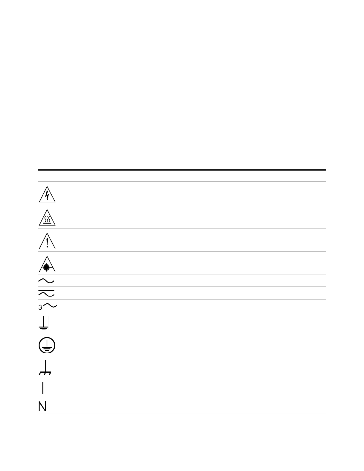
Safety symbols
Safety and Regulatory Information 2
cables to the front panel connectors of the module through
non-conductive, flexible conduit such as that used in electrical
power distribution.
Safety Symbols and Regulatory Markings
Symbols and markings on the system, in manuals and on instruments alert you to potential risks, provide information about
conditions, and comply with international regulations. Table 2-2
defines the symbols and markings you may find in a manual or
on an instrument.
Table 2-2 Safety Symbols and Regulatory Markings
Warning: risk of electric shock.
Warning: hot surface
Caution: refer to accompanying documents.
Laser radiation symbol: marked on products that have a laser output.
Alternating current.
Both direct and alternating current.
Three-phase alternating current.
Earth (ground) terminal
Protective earth (ground) terminal
Frame or chassis terminal
Terminal is at earth potential. Used for measurement and control circuits designed to be operated
with one terminal at earth potential.
Terminal for neutral conductor on permanently installed equipment.
TS-8900 Functional Test System Diagnostics User Guide 2-5
Page 18
2 Safety and Regulatory Information
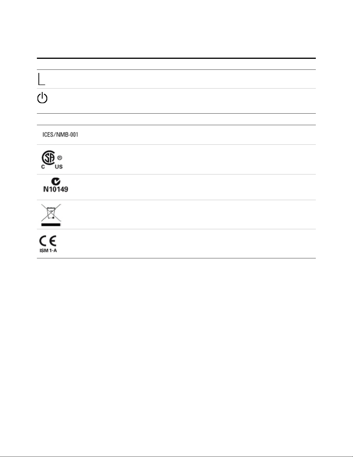
Safety symbols
Terminal for line conductor on permanently installed equipment.
Standby (supply); units with this symbol are not completely disconnected from ac mains when
this switch is off. To completely disconnect the unit from ac mains, either disconnect the power
cord, or have a qualified electrician install an external switch.
Regulatory markings
This text indicates that the ISM device complies with Canadian ICES-001. Cet appareil ISM est
conforme à la norme NMB-001 du Canada.
The CSA mark is a registered trademark of the Canadian Standards Association.
The C-tick mark is a registered trademark of the Spectrum Management Agency of Australia. This
signifies compliance with the Australian EMC Framework regulations under the terms of the
Radio Communications Act of 1992.
This instrument complies with the WEEE Directive (2002/96/EC) marking requirement. This
affixed product label indicates that you must not discard this electrical/electronic product in
domestic householdwaste.
The CE mark is a registered trademark of the European Community. If it is accompanied by a year,
it indicates the year the design was proven.
2-6 TS-8900 Functional Test System Diagnostics User Guide
Page 19
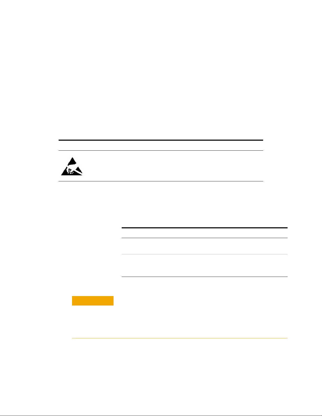
Electrostatic Discharge (ESD) Precautions
CAUTION
Static electricity is destructive to your production process and
the TS-8900. Careless handling and poor site planning can cause
system reliability problems and reduce your product yield. The
system may not be as easily damaged as the modules you will be
testing, but good anti-static planning will help ensure high reliability.
The ESD symbol below indicates areas where ESD caution must
be exercised. This is to prevent damage to instruments and/or
test disruption.
ESD Symbol
Caution: Static Sensitive.
Electrostatic discharge in this area may cause equipment damage or test
disruption.
Safety and Regulatory Information 2
While not an exhaustive list of anti-static precautions, Table 2-3
shows suggestions to consider as you plan your system area:
Table 2-3 Suggested Anti-Static Solutions for Site Planning
Precaution Suggested Solution
Anti-static flooring Plan to use an anti-static floor
covering or mats.
Grounding straps Plan for foot straps in conjunction
with anti-static flooring and wrist
straps for system operators.
The system test rack is secured to the pallet of the shipping crate
and wrapped with a plastic wrap. Do not move the crate or the test
rack and pallet to a static sensitive area until you have removed the
plastic wrap from the test rack.
TS-8900 Functional Test System Diagnostics User Guide 2-7
Page 20
2 Safety and Regulatory Information
End of Life: Waste Electrical and Electronic Equipment (WEEE) Directive 2002/96/EC
This product complies with the WEEE Directive (2002/96/EC)
marking requirement. The affixed product label (see below)
indicates that you must not discard this electrical/electronic
product in domestic household waste.
Product Category:
With reference to the equipment types in the WEEE directive
Annex 1, this product is classified as a “Monitoring and Control
Instrumentation” product.
Do not dispose in domestic household waste
To return unwanted products, contact your local Agilent office,
or see:
http://www. agilent. com/environment/product
for more information.
2-8 TS-8900 Functional Test System Diagnostics User Guide
Page 21
Agilent TS-8900 Functional Test System
NOTE
Diagnostics User Guide
3
Running Diagnostics
Overview of Diagnostics Testplans 3-2
Configuring and Running the DGN Testplan 3-3
Configuring and Running the CEDGN Testplan 3-5
Installing the Diagnostic Test Fixture 3-8
Resolving Test Failures 3-12
This chapter describes the overview of diagnostic testplans, DGN
testplan, CEDGN testplan and how to use the diagnostics test fixtures to
verify the operation of system equipment.
Diagnostic testing is intended to verify basic connectivity and instrument
functionality. It does not provide a full functional test of instrumentation
and specifications.
Agilent Technologies
3-1
Page 22

3 Running Diagnostics
NOTE
Overview of Diagnostics Testplans
The verification strategy incorporates both standard and
optional tests using different testplans. The standard testplan
is shipped with each system. The testplans for the optional
tests are included with the diagnostic test fixtures.
The standard tests verify both the core system instrument
operation and internal test paths. It uses a testplan called
"U8971A_DGN.tpa", simply called "DGN". "DGN" does not
require external hardware, but verifies about 80% of the system
functionality. These testplans are located in directory:
C:\Program Files\Agilent\TS-5000 System Software\testplan\
DGN\
For more detailed description of the "DGN" testplan, go to Diagnostic
Testing Details.
The tests uses the "Customer Engineer Diagnostics" testplans
(file name: "CEDGN *.tpa"), simply called "CEDGN". "CEDGN"
completes the test coverage. It uses optional test hardware that
is supplied with the kit. An understanding of test system
operation and interpreting "CEDGN" test results are required to
execute the tests. These testplans are located in directory:
C:\Program Files\Agilent\TS-5000 System Software\Service\
U8970A\Testplans\
The tests are executed in Agilent TestExec SL and TS-5000
system programming environment, and use both standard and
specialized test actions. The programs can be edited to improve
and/or reduce test coverage. Systems equipped with
non-standard equipment do not have tests incorporated in
either "DGN" or "CEDGN". You have to add tests for those
systems.
3-2 TS-8900 Functional Test System Diagnostics User Guide
Page 23

Configuring and Running the DGN Testplan
1 Start Agilent Test Exec SL by clicking this icon on the
desktop:
2 Load "U8971A_DGN.tpa" testplan into TestExec SL. "DGN"
Testplans are located in this directory:
C:\Program Files\Agilent\TS-5000 System Software\testplan\
DGN\
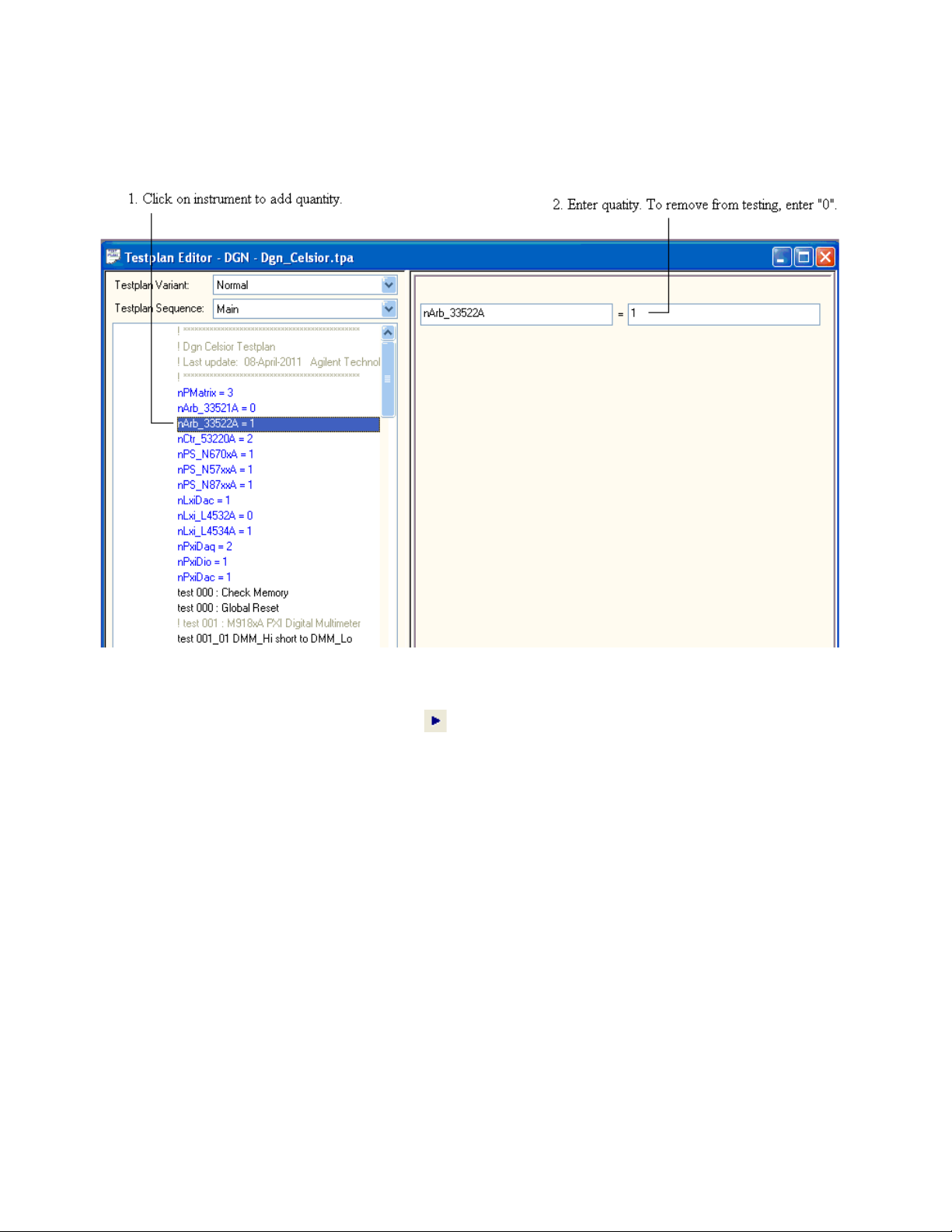
3 Before running the testplan, identify the instrumentation
you want to test in the first lines of the testplan as shown on
Figure 3-1. Place a 1 next to instruments you want to test, a 0
next to those instruments you do not want to test (or that are
not in your system).
Running Diagnostics 3
TS-8900 Functional Test System Diagnostics User Guide 3-3
Page 24
3 Running Diagnostics
Figure 3-1 Specify the Instruments to be Tested in DGN Testplan
4 Click to run the testplan. The testplan will run tests on
each system instrument configuration specified in step 3 and
display the results of the testing.
3-4 TS-8900 Functional Test System Diagnostics User Guide
Page 25
Running Diagnostics 3
Configuring and Running the CEDGN Testplan
1 Start Agilent Test Exec SL by clicking this icon on the
desktop:
2 There are multiple testplans for TS-8900 Functional Test
Systems. The each testplan is for specific instrument, module
or card that is accessible at the Express Connect interface.
Tab le 3- 1 CEDGN Testplan Description and Flow
Testplan Filename Topology filename Description
CEDGN_E878XA_PinMatrix.tpa CEDGN_E878XA_PinMatrix.ust SLU E8782A/E8783A Pin Matrix Card CEDGN Test
CEDGN_E6175A_LoadCard.tpa CEDGN_E6175A_LoadCard.ust SLU E6175A 8 Channel Load Card Test
CEDGN_U7177A_LoadCard.tpa CEDGN_U7177A_LoadCard.ust SLU U7177A 24 Channel Load Card CEDGN Test
CEDGN_E6178B_LoadCard.tpa CEDGN_E6178B_LoadCard.ust SLU E6178B 8 Channel Hi Power Load Card Test
CEDGN_N9377A_LoadCard.tpa CEDGN_N9377A_LoadCard.ust SLU N9377A 16 Channel Load Card CEDGN Test
CEDGN_N9379A_LoadCard.tpa CEDGN_N9379A_LoadCard.ust SLU N9379A 48 Channel Load Card CEDGN Test
CEDGN_E6198B_Utility.tpa CEDGN_E6198B_Utility.ust E6198B SLU Mainframe Utility CEDGN Test
CEDGN_L4451A_LXIDAC.tpa CEDGN_L4451A_LXIDAC.ust LXI L4451A 4 Channel DAC CEDGN Test
CEDGN_M9185A_DAC.tpa CEDGN_M9185A_DAC.ust PXI M9185A 8/16 Channel DAC CEDGN Test
CEDGN_M9186A_VI.tpa CEDGN_M9186A_VI.ust PXI M9186A Voltage Current Source CEDGN Test
CEDGN_M9187A_DIO.tpa CEDGN_M9187A_DIO.ust PXI M9187A Digital IO CEDGN Test
CEDGN_M9216A_DAQ.tpa CEDGN_M9216A_DAQ.ust PXI M9216A HV DAQ CEDGN Test
CEDGN_RS232.tpa CEDGN_RS232.ust RS-232 COM port CEDGN Test
CEDGN_SoftingCAN.tpa CEDGN_SoftingCAN.ust Softing CAN CEDGN Test
3 Load the appropriate testplan and its corresponding
topology file based on your installed hardware into TestExec
SL.
Testplans are located in this directory:
C:\Program Files\Agilent\TS-5000 System Software\Service\
U8970A\Testplans
Topology files are located in this directory:
TS-8900 Functional Test System Diagnostics User Guide 3-5
Page 26

3 Running Diagnostics
C:\Program Files\Agilent\TS-5000 System Software\Service\
U8970A\Ust
4 Load the topology file (*. ust) of the hardware to be tested
and edit the Modules folder content:
• Disable - Check to disable. Uncheck to enable. Depends on
availability of the module in the system.
• Set "Slot #" - Depends on the slot number the card is
installed on the Switch Load Unit. (Applicable to SLU
cards only)
• Set "Instrument Descriptor/Resource" - LXI, PXI, GPIB
module address. Obtained from Agilent IO Libraries Suite.
(VISA Address)
• Set "PCI Slot Number" and "Serial Number" - Depends on
the installed Softing CAN.
Once complete editing, save and close the topology file.
5 Load the testplan together with its corresponding topology
file. Before running the testplan, identify the
instrumentation configuration you want to test in the first
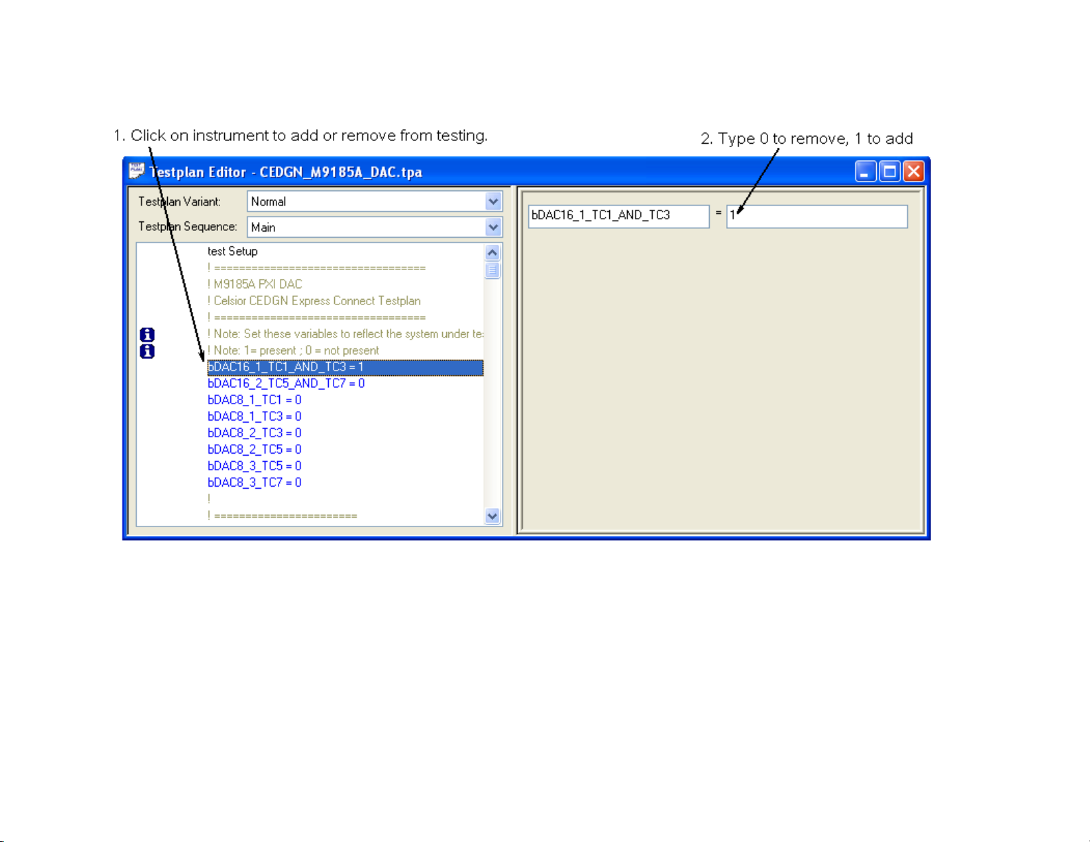
lines of the testplan as shown on Figure 3-2. Place a 1 next to
instrument configuration you want to test, a 0 next to those
instrument configurations you do not want to test (or that
are not in your system).
6 Click to run the testplan. The testplan will run tests on
each system instrument configuration specified in step 5 and
display the results of the testing.
7 Follow the instructions appearing on the display throughout
the test.
8 Repeat step 4 until all instrumentation available in your
system are tested.
3-6 TS-8900 Functional Test System Diagnostics User Guide
Page 27
TS-8900 Functional Test System Diagnostics User Guide 3-7
Figure 3-2 Specify the Instruments to be Tested in CEDGN Testplan
Running Diagnostics 3
Page 28

3 Running Diagnostics
Installing the Diagnostic Test Fixture
While running the CEDGN testplan, specific diagnostic test
fixtures are required to install on the Test System Interface
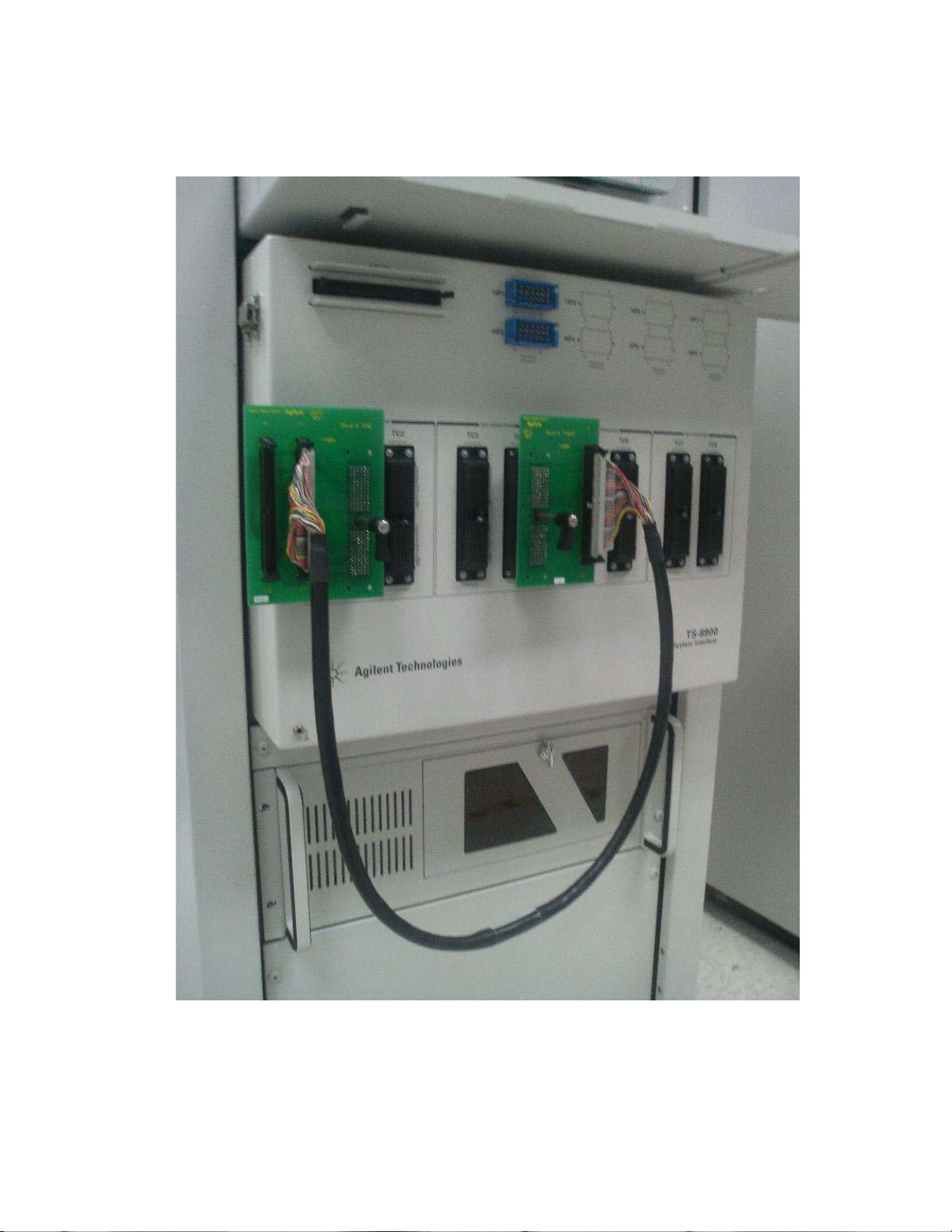
based on the message prompted. Figure 3-3 shows the CEDGN
Board #1 (U8970-66603) to TC1 and CEDGN Board #3
(U8970-66605) to TC4. Both boards are linked by Cable
(E6170-61607). This fixture configuration is used to test the
connectivity and instrumentations functionality in TC4.
3-8 TS-8900 Functional Test System Diagnostics User Guide
Page 29
Running Diagnostics 3
Figure 3-3 Installing CEDGN Board #1 (U8970-66603) to TC1 and CEDGN Board #3 (U8970-66605) to TC4 with
both boards linked by cable (E6170-61607).
TS-8900 Functional Test System Diagnostics User Guide 3-9
Page 30

3 Running Diagnostics
Figure 3-4 shows connection of 8-Ch Heavy Duty Card
diagnostic cable E6170-61618. The Positronic connector on HP2
and cable to Abuses. This diagnostic cable is used to test the
connectivity of 8-Ch Heavy Duty Card on HP2.
3-10 TS-8900 Functional Test System Diagnostics User Guide
Page 31

Running Diagnostics 3
Figure 3-4 Installing 8-Ch Heavy Duty Card diagnostic cable E6170-61618 on HP2 and BNC connectors to
Abus1, Abus2, Abus3 and Abus4.
TS-8900 Functional Test System Diagnostics User Guide 3-11
Page 32

3 Running Diagnostics
Resolving Test Failures
Test failures can be caused by improper switch settings on the
Diagnostic Test Fixture, improper system equipment
specification, or the actual test system instrument failure.
Before troubleshooting the system equipment, make sure the
test fixture switches are properly set and the test system
instrumentation is properly specified. If the problem appears to
be system equipment, swap the instrument and/or the cable
between the instrument and the Test System Interface.
Chapter 4 contains detailed descriptions of each test that may
help in isolating equipment problems to a particular
component.
3-12 TS-8900 Functional Test System Diagnostics User Guide
Page 33

Agilent TS-8900 Functional Test System
Diagnostics User Guide
4
Diagnostic Testing Details
DGN Testplan Description and Flow 4-2
Test Fixture Description 4-15
CEDGN Testplan Description and Flow 4-21
Agilent Technologies
4-1
Page 34

4 Diagnostic Testing Details
NOTE
NOTE
DGN Testplan Description and Flow
The standard DGN diagnostic program consists of tests
designed for specific system subassemblies. Generally, DGN
tests are organized as follows:
• System reset.
• Test of other instruments, such as tests of the E6198A
Switch/Load Unit , 3352xA Arbitrary Waveform Generator , 53220A
Counter, power supply, and etc.
• Several tests dedicated to Pin Matrix Modules - open/close relay
tests.
• Tests of PXI modules, such as M9186A DAQ, M9185A 8/16-CH
DAC, M9187A IO and etc.
Load cards are not tested by DGN.
L4451A LXI DAC and PXI module(s) functionality is not tested by DGN.
Test 000: Check Memory
Test 000: Global reset
• This test group gets IPC information, initializes and resets all
instruments in the system configuration editor (SCE).
Test 001: M918xA PXI Digital Multimeter
Test 001: ABUS 1, 2, 3, 4
• This test group verifies DMM_Hi and DMM_Lo connection and
ABUS float for ABUS 1, 2, 3 and 4.
Test 002: E6198B Agilent Switch/Load unit
• This test group measures SLU DAC#1 & DAC#2 output.
4-2 TS-8900 Functional Test System Diagnostics User Guide
Page 35

Diagnostic Testing Details 4
Test 003: 335xA GPIB Arbitrary Waveform Generator
• This tests group consists of 2 tests. First test is performing
instrument self test, waits for the instrument to complete the test,
and queries the instrument for the results. Second test is
generating 5V from Arbitrary Waveform Generator and measure
using DMM as shown in Figure 4-1 below.
TS-8900 Functional Test System Diagnostics User Guide 4-3
Page 36

4-4 TS-8900 Functional Test System Diagnostics User Guide
4 Diagnostic Testing Details
Figure 4-1 Generate 5V from Arbitrary Waveform Generator and measure using DMM.
Page 37

Diagnostic Testing Details 4
Test 004: 53220A GPIB Universal Frequency Counter
• This test group consists of 3 tests. First test is performing
instrument self test, waits for the instrument to complete the test,
and queries the instrument for the results.
• For second test, counter is connected to the DMM. The counter
output is enabled and the expected 50 ohms resistance present in
matrix path is measured using the DMM and compared to limits.
Next, the counter’s output is disabled and a High Z resistance
measurement is made and compared against limits. Figure 4-2
illustrates this test for Channel 1.
TS-8900 Functional Test System Diagnostics User Guide 4-5
Page 38

4-6 TS-8900 Functional Test System Diagnostics User Guide
4 Diagnostic Testing Details
Figure 4-2 Test Counter 50 Ohm and Hi Z for Channel1.
Page 39

Diagnostic Testing Details 4
• Third test is required only if ARB is present. The counter output is
connected to the ARB output and measures the output signal
properties. See Figure 4-3 below.
TS-8900 Functional Test System Diagnostics User Guide 4-7
Page 40

4-8 TS-8900 Functional Test System Diagnostics User Guide
4 Diagnostic Testing Details
Figure 4-3 Counter measures Arbitrary Waveform Generator output signal properties.
Page 41

Diagnostic Testing Details 4
Test 005: L4451A LXI Digital/Analog Converter
• This test group performs instrument self test, waits for the
instrument to complete the test, and queries the instrument for the
results.
Test 006: L453xA LXI Digitizer
• This test group consists of 3 tests. First test performs instrument
self test, waits for the instrument to complete the test, and queries
the instrument for the results.
• The second test is required only if ARB is present. The digitizer
output is connected to the ARB output and captures the output
signal properties. See Figure 4-4 below.
TS-8900 Functional Test System Diagnostics User Guide 4-9
Page 42

4-10 TS-8900 Functional Test System Diagnostics User Guide
4 Diagnostic Testing Details
Figure 4-4 Digitizer captures Arbitrary Waveform Generator output signal properties.
Page 43

Diagnostic Testing Details 4
Test 007: Power Supply
• This test group performs instrument self test, waits for the
instrument to complete the test, and queries the instrument for the
results. Repeat test for all selected Agilent power supply.
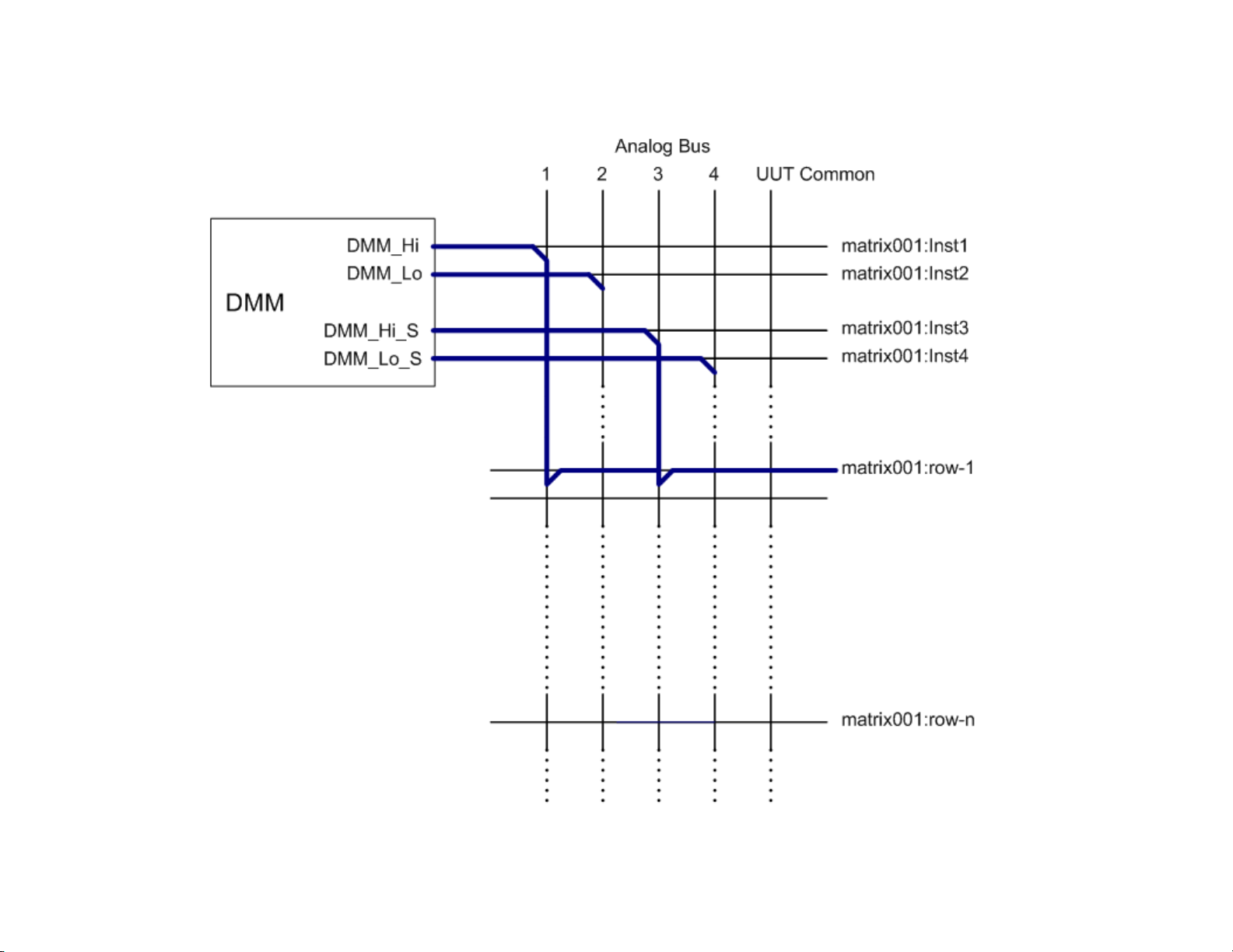
Test 008: Pin Matrix Relay Open/Close
• This test group consists of matrix row close and open tests.
Figure 4-5 and Figure 4-6 illustrate measure short and open by
DMM for matrix001:row-1 to matrix001:row-n, where n = 2, 3. . . 63,
64.
TS-8900 Functional Test System Diagnostics User Guide 4-11
Page 44

4-12 TS-8900 Functional Test System Diagnostics User Guide
4 Diagnostic Testing Details
Figure 4-5 Measure short by DMM for matrix row 1 and matrix row-n open.
Page 45
TS-8900 Functional Test System Diagnostics User Guide 4-13
Figure 4-6 Measure open by DMM for matrix row 1 and matrix row-n open.
Diagnostic Testing Details 4
Page 46

4 Diagnostic Testing Details
Test 009: M9216A PXI Data Acquisition (DAQ)
Test 009: M9187A PXI Digital IO
Test 009: M9185A PXI Digital/Analog Converter
• This test group gets information from each selected PXI modules.
4-14 TS-8900 Functional Test System Diagnostics User Guide
Page 47

Test Fixture Description
U8970-66603 PCA-DIAGNOSTIC NUMBER 1 (Board #1)
Diagnostic Testing Details 4
The test system uses Express Connect interface, test fixtures
below are required to run the CEDGN testplans. Refer to
Appendix A for more details.
Figure 4-7 CEDGN Board #1 (U8970-66603 PCA- Diagnostic Number 1)
TS-8900 Functional Test System Diagnostics User Guide 4-15
Page 48

4 Diagnostic Testing Details
U8970-66604 PCA-DIAGNOSTIC NUMBER 2 (Board #2)
Figure 4-8 CEDGN Board #2 (U8970-66604 PCA- Diagnostic Number 2)
U8970-66605 PCA-DIAGNOSTIC NUMBER 3 (Board #3)
Figure 4-9 CEDGN Board #3 (U8970-66605 PCA- Diagnostic Number 3)
4-16 TS-8900 Functional Test System Diagnostics User Guide
Page 49

Diagnostic Testing Details 4
U8970-66606 PCA-DIAGNOSTIC NUMBER 4 (Board #4)
Figure 4-10 CEDGN Board #4 (U8970-66606 PCA- Diagnostic Number 4)
U8970-66607 PCA-DIAGNOSTIC NUMBER 5 (Board #5)
Figure 4-11 CEDGN Board #5 (U8970-66607 PCA- Diagnostic Number 5)
TS-8900 Functional Test System Diagnostics User Guide 4-17
Page 50

4 Diagnostic Testing Details
E6170-61607 CABLE 2X 2X32 IDC PIN 1 TO PIN 1
Figure 4-12 CEDGN Cable (E6170-61607 Cable 2X 2X32 IDC Pin 1 To Pin 1)
E6170-61618 Diagnostic Cable
Figure 4-13 Diagnostic Cable (E6170-61618) for 8 Channel Heavy Duty
Card
4-18 TS-8900 Functional Test System Diagnostics User Guide
Page 51

E2240-67012 CEDGN LOOPBACK CONNECTOR
Diagnostic Testing Details 4
Figure 4-14 CEDGN Loopback Connector (E2240-67012) CEDGN test load
module for E6175A, U7177A, and N9377A
E6170-66520 820OHM LOADED MEZZANINE CARD
Figure 4-15 820OHM Loaded Mezzanine Card (E6170-66520) CEDGN test
load module for N9379A
TS-8900 Functional Test System Diagnostics User Guide 4-19
Page 52

4 Diagnostic Testing Details
E6170-61619 CABLE-HEAVY DUTY LOAD JUMPER
Figure 4-16 Heavy Duty Load Card Load Loopback (E6170-61619) CEDGN
test load for E6178B
4-20 TS-8900 Functional Test System Diagnostics User Guide
Page 53

Diagnostic Testing Details 4
CEDGN Testplan Description and Flow
There are multiple testplans for TS-8900 Functional Test
System. Each testplan tests specific instrument / module / card.
Each testplan is accompanied by a topolgy file.
Below is the list of CEDGN testplans.
Tab le 4- 1 CEDGN Testplan Description and Flow
Testplan Filename Topology filename Description
CEDGN_E878XA_PinMatrix.tpa CEDGN_E878XA_PinMatrix.ust SLU E8782A/E8783A Pin Matrix Card CEDGN Test
CEDGN_E6175A_LoadCard.tpa CEDGN_E6175A_LoadCard.ust SLU E6175A 8 Channel Load Card Test
CEDGN_U7177A_LoadCard.tpa CEDGN_U7177A_LoadCard.ust SLU U7177A 24 Channel Load Card CEDGN Test
CEDGN_E6178B_LoadCard.tpa CEDGN_E6178B_LoadCard.ust SLU E6178B 8 Channel Hi Power Load Card Test
CEDGN_N9377A_LoadCard.tpa CEDGN_N9377A_LoadCard.ust SLU N9377A 16 Channel Load Card CEDGN Test
CEDGN_N9379A_LoadCard.tpa CEDGN_N9379A_LoadCard.ust SLU N9379A 48 Channel Load Card CEDGN Test
CEDGN_E6198B_Utility.tpa CEDGN_E6198B_Utility.ust E6198B SLU Mainframe Utility CEDGN Test
CEDGN_L4451A_LXIDAC.tpa CEDGN_L4451A_LXIDAC.ust LXI L4451A 4 Channel DAC CEDGN Test
CEDGN_M9185A_DAC.tpa CEDGN_M9185A_DAC.ust PXI M9185A 8/16 Channel DAC CEDGN Test
CEDGN_M9186A_VI.tpa CEDGN_M9186A_VI.ust PXI M9186A Voltage Current Source CEDGN Test
CEDGN_M9187A_DIO.tpa CEDGN_M9187A_DIO.ust PXI M9187A Digital IO CEDGN Test
CEDGN_M9216A_DAQ.tpa CEDGN_M9216A_DAQ.ust PXI M9216A HV DAQ CEDGN Test
CEDGN_RS232.tpa CEDGN_RS232.ust RS-232 COM port CEDGN Test
CEDGN_SoftingCAN.tpa CEDGN_SoftingCAN.ust Softing CAN CEDGN Test
The following paragraphs describe the test flow of each
testplan.
TS-8900 Functional Test System Diagnostics User Guide 4-21
Page 54

4 Diagnostic Testing Details
CEDGN_E878XA_PinMatrix.tpa (Pin Matrix CEDGN Test Flow)
The testsplan supports testing of one E8782A and four E8783A
Pin Matrix Card. User is required to set the variables to reflect
the system under test.
1 = present, 0 = not present
bMtrx1 = 1st Pin Matrix E8782A
bMtrx2 = 2ndPin Matrix E8783A
bMtrx3 = 3rd Pin Matrix E8783A
bMtrx4 = 4th Pin Matrix E8783A
bMtrx5 = 5th Pin Matrix E8783A
Device that user sets as not present will not be tested. The test
starts by performing:
Not Acceptable Combination Checking
• Checks user settings for any not acceptable combination. Stops
test and provide error message if not acceptable selection is found.
Matrix1 E8782A on TC1 Tests
• Display instruction to Install CEDGN Board #5 on TC1. S1 and S2
on CEDGN Board #5 are all toggled to ON (CLOSE).
• Setup DMM for 4W resistance measurement.
• Perform Matrix1 loopback resistance measurements between
Row1-Row2, Row3-Row4, until Row31-Row32.
Matrix2 Row1-Row32
• Display instruction to Install CEDGN Board #5 on appropriate TC.
S1 and S2 on CEDGN Board #5 are all toggled to ON (CLOSE).
Matrix2 E8783A Row1-Row32 Tests
• Setup DMM for 4W resistance measurement.
• Perform Matrix2 loopback resistance measurements between
Row1-Row2, Row3-Row4, until Row31-Row32.
Matrix2 Row33-Row64
• Display instruction to Install CEDGN Board #5 on appropriate TC.
S1 and S2 on CEDGN Board #5 are all toggled to ON (CLOSE).
4-22 TS-8900 Functional Test System Diagnostics User Guide
Page 55

Diagnostic Testing Details 4
Matrix2 E8783A Row33-Row64 Tests
• Setup DMM for 4W resistance measurement.
• Perform Matrix2 loopback resistance measurements between
Row33-Row34, Row35-Row36, until Row63-Row64.
Matrix3 Row1-Row32
• Display instruction to Install CEDGN Board #5 on appropriate TC.
S1 and S2 on CEDGN Board #5 are all toggled to ON (CLOSE).
Matrix3 E8783A Row1-Row32 Tests
• Setup DMM for 4W resistance measurement.
• Perform Matrix3 loopback resistance measurements between
Row1-Row2, Row3-Row4, until Row31-Row32.
Matrix3 Row33-Row64
• Display instruction to Install CEDGN Board #5 on appropriate TC.
S1 and S2 on CEDGN Board #5 are all toggled to ON (CLOSE).
Matrix3 E8783A Row33-Row64 Tests
• Setup DMM for 4W resistance measurement.
• Perform Matrix3 loopback resistance measurements between
Row33-Row34, Row35-Row36, until Row63-Row64.
Matrix4 Row1-Row32
• Display instruction to Install CEDGN Board #5 on appropriate TC.
S1 and S2 on CEDGN Board #5 are all toggled to ON (CLOSE).
Matrix4 E8783A Row1-Row32 Tests
• Setup DMM for 4W resistance measurement.
• Perform Matrix4 loopback resistance measurements between
Row1-Row2, Row3-Row4, until Row31-Row32.
Matrix4 Row33-Row64
• Display instruction to Install CEDGN Board #5 on appropriate TC.
S1 and S2 on CEDGN Board #5 are all toggled to ON (CLOSE).
TS-8900 Functional Test System Diagnostics User Guide 4-23
Page 56

4 Diagnostic Testing Details
Matrix4 E8783A Row33-Row64 Tests
• Setup DMM for 4W resistance measurement.
• Perform Matrix4 loopback resistance measurements between
Row33-Row34, Row35-Row36, until Row63-Row64.
Matrix5 Row1-Row32
• Display instruction to Install CEDGN Board #5 on TC8. S1 and S2
on CEDGN Board #5 are all toggled to ON (CLOSE).
Matrix5 E8783A Row1-Row32 Tests
• Setup DMM for 4W resistance measurement.
• Perform Matrix5 loopback resistance measurements between
Row1-Row2, Row3-Row4, until Row31-Row32.
Matrix 1 Aux 1-8 Testing
• Display instruction to Install CEDGN Board #2 on TC1. S1 and S2
on CEDGN Board #2 are toggle to DOWN position.
• Setup DMM for 4W resistance measurement.
• Perform Matrix1 loopback resistance measurements between
Aux1-Aux2, Aux3-Aux4, Aux5-Aux6 and Aux7-Aux8.
Matrix 1 Aux 33-40 Testing
• Display instruction to Install CEDGN Board #2 on TC3. S1 and S2
on CEDGN Board #2 are toggle to DOWN position.
• Setup DMM for 4W resistance measurement.
• Perform Matrix1 loopback resistance measurements between
Aux33-Aux34, Aux35-Aux36, Aux37-Aux38 and Aux39-Aux40.
Matrix 2 Aux 1-8 Testing
• Display instruction to Install CEDGN Board #2 on TC5. S1 and S2
on CEDGN Board #2 are toggle to DOWN position.
• Setup DMM for 4W resistance measurement.
• Perform Matrix2 loopback resistance measurements between
Aux1-Aux2, Aux3-Aux4, Aux5-Aux6 and Aux7-Aux8.
4-24 TS-8900 Functional Test System Diagnostics User Guide
Page 57

Diagnostic Testing Details 4
Matrix 2 Aux 33-40 Testing
• Display instruction to Install CEDGN Board #2 on TC7. S1 and S2
on CEDGN Board #2 are toggle to DOWN position.
• Setup DMM for 4W resistance measurement.
• Perform Matrix2 loopback resistance measurements between
Aux33-Aux34, Aux35-Aux36, Aux37-Aux38 and Aux39-Aux40.
Figure 4-17 Pin Matrix Loopback Test
TS-8900 Functional Test System Diagnostics User Guide 4-25
Page 58

4 Diagnostic Testing Details
CEDGN_E6175A_LoadCard.tpa (8 Channel Load Card CEDGN Test Flow)
The testsplan supports testing of eight E6175A Load Cards.
User is required to set the variables to reflect the system under
test.
1 = present, 0 = not present
bLC8CH_1 = 1st E6175A
bLC8CH_2 = 2nd E6175A
bLC8CH_3 = 3rd E6175A
bLC8CH_4 = 4th E6175A
bLC8CH_5 = 5th E6175A
bLC8CH_6 = 6th E6175A
bLC8CH_7 = 7th E6175A
bLC8CH_8 = 8th E6175A
Device that user sets as not present will not be tested. The test
starts by performing:
Not Acceptable Combination Checking
• Checks user settings for any not acceptable combination. Stops
test and provide error message if not acceptable selection is found.
E6175A 8 Channel Load Card LC8CH_1 Tests
• Display instruction to Install load module E2240-67012 on LC8CH_1
Load Card.
• For LC8CH_1 on TC1, display instruction to install CEDGN Board
#4 on TC1 and Cable E6170-61607 from SLU Utility Connector to J2
of Board #4.
• For LC8CH_1 on other TC, display instruction to install CEDGN
Board #1 on TC1 and CEDGN Board #4 on appropriate TC. Install
Cable E6170-61607 from SLU Utility Connector to J2 of Board #4.
Install Cable E6170-61607 from J1 of Board #1 to J1 of Board #4.
• Setup DMM to perform 2W resistance measurement.
• Measure LC8CH_1 load card loopback path resistance from
CH1-CH5, CH2-CH6, CH3-CH7 and CH4-CH8 via Row1 and Row2.
• Measure LC8CH_1 load card sense resistor path:
CH1 & CH2 Current Sense, CH3 & CH4 Current Sense, CH5 & CH6
Current Sense, and CH7 & CH8 Current Sense via Row25 and
Row26.
4-26 TS-8900 Functional Test System Diagnostics User Guide
Page 59

Diagnostic Testing Details 4
E6175A 8 Channel Load Card LC8CH_2 Tests
• Display instruction to Install load module E2240-67012 on LC8CH_2
Load Card.
• Display instruction to install CEDGN Board #1 on TC1 and CEDGN
Board #4 on appropriate TC. Install Cable E6170-61607 from SLU
Utility Connector to J2 of Board #4. Install Cable E6170-61607 from
J1 of Board #1 to J1 of Board #4.
• Setup DMM to perform 2W resistance measurement.
• Measure LC8CH_2 load card loopback path resistance from
CH1-CH5, CH2-CH6, CH3-CH7 and CH4-CH8 via Row1 and Row2.
• Measure LC8CH_2 load card sense resistor path:
CH1 & CH2 Current Sense, CH3 & CH4 Current Sense, CH5 & CH6
Current Sense, and CH7 & CH8 Current Sense via Row25 and
Row26.
E6175A 8 Channel Load Card LC8CH_3 Tests
• Display instruction to Install load module E2240-67012 on LC8CH_3
Load Card.
• Display instruction to install CEDGN Board #1 on TC1 and CEDGN
Board #4 on appropriate TC. Install Cable E6170-61607 from SLU
Utility Connector to J2 of Board #4. Install Cable E6170-61607 from
J1 of Board #1 to J1 of Board #4.
• Setup DMM to perform 2W resistance measurement.
• Measure LC8CH_3 load card loopback path resistance from
CH1-CH5, CH2-CH6, CH3-CH7 and CH4-CH8 via Row1 and Row2.
• Measure LC8CH_3 load card sense resistor path:
CH1 & CH2 Current Sense, CH3 & CH4 Current Sense, CH5 & CH6
Current Sense, and CH7 & CH8 Current Sense via Row25 and
Row26.
E6175A 8 Channel Load Card LC8CH_4 Tests
• Display instruction to Install load module E2240-67012 on LC8CH_4
Load Card.
• Display instruction to install CEDGN Board #1 on TC1 and CEDGN
Board #4 on appropriate TC. Install Cable E6170-61607 from SLU
Utility Connector to J2 of Board #4. Install Cable E6170-61607 from
J1 of Board #1 to J1 of Board #4.
• Setup DMM to perform 2W resistance measurement.
• Measure LC8CH_4 load card loopback path resistance from
CH1-CH5, CH2-CH6, CH3-CH7 and CH4-CH8 via Row1 and Row2.
TS-8900 Functional Test System Diagnostics User Guide 4-27
Page 60

4 Diagnostic Testing Details
• Measure LC8CH_4 load card sense resistor path:
CH1 & CH2 Current Sense, CH3 & CH4 Current Sense, CH5 & CH6
Current Sense, and CH7 & CH8 Current Sense via Row25 and
Row26.
E6175A 8 Channel Load Card LC8CH_5 Tests
• Display instruction to Install load module E2240-67012 on LC8CH_5
Load Card.
• Display instruction to install CEDGN Board #1 on TC1 and CEDGN
Board #4 on appropriate TC. Install Cable E6170-61607 from SLU
Utility Connector to J2 of Board #4. Install Cable E6170-61607 from
J1 of Board #1 to J1 of Board #4.
• Setup DMM to perform 2W resistance measurement.
• Measure LC8CH_5 load card loopback path resistance from
CH1-CH5, CH2-CH6, CH3-CH7 and CH4-CH8 via Row1 and Row2.
• Measure LC8CH_5 load card sense resistor path:
CH1 & CH2 Current Sense, CH3 & CH4 Current Sense, CH5 & CH6
Current Sense, and CH7 & CH8 Current Sense via Row25 and
Row26.
E6175A 8 Channel Load Card LC8CH_6 Tests
• Display instruction to Install load module E2240-67012 on LC8CH_6
Load Card.
• Display instruction to install CEDGN Board #1 on TC1 and CEDGN
Board #4 on appropriate TC. Install Cable E6170-61607 from SLU
Utility Connector to J2 of Board #4. Install Cable E6170-61607 from
J1 of Board #1 to J1 of Board #4.
• Setup DMM to perform 2W resistance measurement.
• Measure LC8CH_6 load card loopback path resistance from
CH1-CH5, CH2-CH6, CH3-CH7 and CH4-CH8 via Row1 and Row2.
• Measure LC8CH_6 load card sense resistor path:
CH1 & CH2 Current Sense, CH3 & CH4 Current Sense, CH5 & CH6
Current Sense, and CH7 & CH8 Current Sense via Row25 and
Row26.
4-28 TS-8900 Functional Test System Diagnostics User Guide
Page 61

Diagnostic Testing Details 4
E6175A 8 Channel Load Card LC8CH_7 Tests
• Display instruction to Install load module E2240-67012 on LC8CH_7
Load Card.
• Display instruction to install CEDGN Board #1 on TC1 and CEDGN
Board #4 on appropriate TC. Install Cable E6170-61607 from SLU
Utility Connector to J2 of Board #4. Install Cable E6170-61607 from
J1 of Board #1 to J1 of Board #4.
• Setup DMM to perform 2W resistance measurement.
• Measure LC8CH_7 load card loopback path resistance from
CH1-CH5, CH2-CH6, CH3-CH7 and CH4-CH8 via Row1 and Row2.
• Measure LC8CH_7 load card sense resistor path:
CH1 & CH2 Current Sense, CH3 & CH4 Current Sense, CH5 & CH6
Current Sense, and CH7 & CH8 Current Sense via Row25 and
Row26.
E6175A 8 Channel Load Card LC8CH_8 Tests
• Display instruction to Install load module E2240-67012 on LC8CH_8
Load Card.
• Display instruction to install CEDGN Board #1 on TC1 and CEDGN
Board #4 on appropriate TC. Install Cable E6170-61607 from SLU
Utility Connector to J2 of Board #4. Install Cable E6170-61607 from
J1 of Board #1 to J1 of Board #4.
• Setup DMM to perform 2W resistance measurement.
• Measure LC8CH_8 load card loopback path resistance from
CH1-CH5, CH2-CH6, CH3-CH7 and CH4-CH8 via Row1 and Row2.
• Measure LC8CH_8 load card sense resistor path:
CH1 & CH2 Current Sense, CH3 & CH4 Current Sense, CH5 & CH6
Current Sense, and CH7 & CH8 Current Sense via Row25 and
Row26.
TS-8900 Functional Test System Diagnostics User Guide 4-29
Page 62

4 Diagnostic Testing Details
Figure 4-18 E6175A 8 Channel Load Card Test
4-30 TS-8900 Functional Test System Diagnostics User Guide
Page 63

Diagnostic Testing Details 4
CEDGN_U7177A_LoadCard.tpa (24 Channel Load Card CEDGN Test Flow)
The testsplan supports testing of eight U7177A Load Cards.
User is required to set the variables to reflect the system under
test.
1 = present, 0 = not present
bLC24CH_1 = 1st U7177A
bLC24CH_2 = 2nd U7177A
bLC24CH_3 = 3rd U7177A
bLC24CH_4 = 4th U7177A
bLC24CH_5 = 5th U7177A
bLC24CH_6 = 6th U7177A
bLC24CH_7 = 7th U7177A
bLC24CH_8 = 8th U7177A
Device that user sets as not present will not be tested. The test
starts by performing:
Not Acceptable Combination Checking
• Checks user settings for any not acceptable combination. Stops
test and provide error message if not acceptable selection is found.
U7177A 24 Channel Load Card LC24CH_1 Tests
• Display instruction to Install load module E2240-67012 on
LC24CH_1 Load Card.
• For LC24CH_1 on TC1, display instruction to install CEDGN Board
#4 on TC1 and Cable E6170-61607 from SLU Utility Connector to J2
of Board #4.
• For LC24CH_1 on other TC, display instruction to install CEDGN
Board #1 on TC1 and CEDGN Board #4 on appropriate TC. Install
Cable E6170-61607 from SLU Utility Connector to J2 of Board #4.
Install Cable E6170-61607 from J1 of Board #1 to J1 of Board #4.
• Setup DMM to perform 2W resistance measurement.
• Measure LC24CH_1 load card loopback path resistance from
CH1-Com1 until CH12-Com12 via Row1 and Row8
CH13-Com13 until CH24-Com24 via Row2 and Row7
• Measure LC24CH_1 load card sense resistor path:
CH1 Sense until CH24 Sense via Row25 and Row26.
TS-8900 Functional Test System Diagnostics User Guide 4-31
Page 64

4 Diagnostic Testing Details
U7177A 24 Channel Load Card LC24CH_2 Tests
• Display instruction to Install load module E2240-67012 on
LC24CH_2 Load Card.
• Display instruction to install CEDGN Board #1 on TC1 and CEDGN
Board #4 on appropriate TC. Install Cable E6170-61607 from SLU
Utility Connector to J2 of Board #4. Install Cable E6170-61607 from
J1 of Board #1 to J1 of Board #4.
• Setup DMM to perform 2W resistance measurement.
• Measure LC24CH_2 load card loopback path resistance from
CH1-Com1 until CH12-Com12 via Row1 and Row8
CH13-Com13 until CH24-Com24 via Row2 and Row7
• Measure LC24CH_2 load card sense resistor path:
CH1 Sense until CH24 Sense via Row25 and Row26.
U7177A 24 Channel Load Card LC24CH_3 Tests
• Display instruction to Install load module E2240-67012 on
LC24CH_3 Load Card.
• Display instruction to install CEDGN Board #1 on TC1 and CEDGN
Board #4 on appropriate TC. Install Cable E6170-61607 from SLU
Utility Connector to J2 of Board #4. Install Cable E6170-61607 from
J1 of Board #1 to J1 of Board #4.
• Setup DMM to perform 2W resistance measurement.
• Measure LC24CH_3 load card loopback path resistance from
CH1-Com1 until CH12-Com12 via Row1 and Row8
CH13-Com13 until CH24-Com24 via Row2 and Row7
• Measure LC24CH_3 load card sense resistor path:
CH1 Sense until CH24 Sense via Row25 and Row26.
4-32 TS-8900 Functional Test System Diagnostics User Guide
Page 65

Diagnostic Testing Details 4
U7177A 24 Channel Load Card LC24CH_4 Tests
• Display instruction to Install load module E2240-67012 on
LC24CH_4 Load Card.
• Display instruction to install CEDGN Board #1 on TC1 and CEDGN
Board #4 on appropriate TC. Install Cable E6170-61607 from SLU
Utility Connector to J2 of Board #4. Install Cable E6170-61607 from
J1 of Board #1 to J1 of Board #4.
• Setup DMM to perform 2W resistance measurement.
• Measure LC24CH_4 load card loopback path resistance from
CH1-Com1 until CH12-Com12 via Row1 and Row8
CH13-Com13 until CH24-Com24 via Row2 and Row7
• Measure LC24CH_4 load card sense resistor path:
CH1 Sense until CH24 Sense via Row25 and Row26.
U7177A 24 Channel Load Card LC24CH_5 Tests
• Display instruction to Install load module E2240-67012 on
LC24CH_5 Load Card.
• Display instruction to install CEDGN Board #1 on TC1 and CEDGN
Board #4 on appropriate TC. Install Cable E6170-61607 from SLU
Utility Connector to J2 of Board #4. Install Cable E6170-61607 from
J1 of Board #1 to J1 of Board #4.
• Setup DMM to perform 2W resistance measurement.
• Measure LC24CH_5 load card loopback path resistance from
CH1-Com1 until CH12-Com12 via Row1 and Row8
CH13-Com13 until CH24-Com24 via Row2 and Row7
• Measure LC24CH_5 load card sense resistor path:
CH1 Sense until CH24 Sense via Row25 and Row26.
TS-8900 Functional Test System Diagnostics User Guide 4-33
Page 66

4 Diagnostic Testing Details
U7177A 24 Channel Load Card LC24CH_6 Tests
• Display instruction to Install load module E2240-67012 on
LC24CH_6 Load Card.
• Display instruction to install CEDGN Board #1 on TC1 and CEDGN
Board #4 on appropriate TC. Install Cable E6170-61607 from SLU
Utility Connector to J2 of Board #4. Install Cable E6170-61607 from
J1 of Board #1 to J1 of Board #4.
• Setup DMM to perform 2W resistance measurement.
• Measure LC24CH_6 load card loopback path resistance from
CH1-Com1 until CH12-Com12 via Row1 and Row8
CH13-Com13 until CH24-Com24 via Row2 and Row7
• Measure LC24CH_6 load card sense resistor path:
CH1 Sense until CH24 Sense via Row25 and Row26.
U7177A 24 Channel Load Card LC24CH_7 Tests
• Display instruction to Install load module E2240-67012 on
LC24CH_7 Load Card.
• Display instruction to install CEDGN Board #1 on TC1 and CEDGN
Board #4 on appropriate TC. Install Cable E6170-61607 from SLU
Utility Connector to J2 of Board #4. Install Cable E6170-61607 from
J1 of Board #1 to J1 of Board #4.
• Setup DMM to perform 2W resistance measurement.
• Measure LC24CH_7 load card loopback path resistance from
CH1-Com1 until CH12-Com12 via Row1 and Row8
CH13-Com13 until CH24-Com24 via Row2 and Row7
• Measure LC24CH_7 load card sense resistor path:
CH1 Sense until CH24 Sense via Row25 and Row26.
4-34 TS-8900 Functional Test System Diagnostics User Guide
Page 67

Diagnostic Testing Details 4
U7177A 24 Channel Load Card LC24CH_8 Tests
• Display instruction to Install load module E2240-67012 on
LC24CH_8 Load Card.
• Display instruction to install CEDGN Board #1 on TC1 and CEDGN
Board #4 on appropriate TC. Install Cable E6170-61607 from SLU
Utility Connector to J2 of Board #4. Install Cable E6170-61607 from
J1 of Board #1 to J1 of Board #4.
• Setup DMM to perform 2W resistance measurement.
• Measure LC24CH_8 load card loopback path resistance from
CH1-Com1 until CH12-Com12 via Row1 and Row8
CH13-Com13 until CH24-Com24 via Row2 and Row7
• Measure LC24CH_8 load card sense resistor path:
CH1 Sense until CH24 Sense via Row25 and Row26.
Figure 4-19 U7177A 24 Channel Load Card Test
TS-8900 Functional Test System Diagnostics User Guide 4-35
Page 68

4 Diagnostic Testing Details
CEDGN_E6178B_LoadCard.tpa (8 Channel High Power Load Card CEDGN Test Flo w )
The testsplan supports testing of eight E6178B High Power Load
Cards. User is required to set the variables to reflect the system
under test.
1 = present, 0 = not present
bLC8CH_1 = 1st E6178B
bLC8CH_2 = 2nd E6178B
bLC8CH_3 = 3rd E6178B
bLC8CH_4 = 4th E6178B
bLC8CH_5 = 5th E6178B
bLC8CH_6 = 6th E6178B
bLC8CH_7 = 7th E6178B
bLC8CH_8 = 8th E6178B
Device that user sets as not present will not be tested. The test
starts by performing:
Not Acceptable Combination Checking
• Checks user settings for any not acceptable combination. Stops
test and provide error message if not acceptable selection is found.
4-36 TS-8900 Functional Test System Diagnostics User Guide
Page 69

Diagnostic Testing Details 4
E6178B 8 Channel High Power Load Card LC8CH_1 Tests
• Display instruction to disconnect power supply from (P100)PWR1
and (P200)PWR2 of E6178B_1. Short PWR1 to PWR2 of E6178B_1.
Install load loopback cable E6170-61619 on E6178B_1. Install
Diagnostic Cable (E6170-61618) on appropriate HP connector.
• Setup DMM to perform 2W resistance measurement.
• Measure LC8CH_1 load card loopback path resistance from
CH1-CH2 via Positronic pin5 and pin11 (ABUS1 & ABUS3)
CH1-CH2 via Positronic pin6 and pin12 (ABUS2 & ABUS4)
CH1-CH3 via Positronic pin5 and pin17 (ABUS1 & ABUS3)
CH1-CH3 via Positronic pin6 and pin18 (ABUS2 & ABUS4)
CH1-CH4 via Positronic pin5 and pin3 (ABUS1 & ABUS3)
CH1-CH4 via Positronic pin6 and pin4 (ABUS2 & ABUS4)
CH1-CH5 via Positronic pin5 and pin9 (ABUS1 & ABUS3)
CH1-CH5 via Positronic pin6 and pin10 (ABUS2 & ABUS4)
CH1-CH6 via Positronic pin5 and pin15 (ABUS1 & ABUS3)
CH1-CH6 via Positronic pin6 and pin16 (ABUS2 & ABUS4)
CH1-CH7 via Positronic pin5 and pin1 (ABUS1 & ABUS3)
CH1-CH7 via Positronic pin6 and pin2 (ABUS2 & ABUS4)
CH1-CH8 via Positronic pin5 and pin7 (ABUS1 & ABUS3)
CH1-CH8 via Positronic pin6 and pin8 (ABUS2 & ABUS4)
E6178B 8 Channel High Power Load Card LC8CH_2 Tests
• Display instruction to disconnect power supply from (P100)PWR1
and (P200)PWR2 of E6178B_2. Short PWR1 to PWR2 of E6178B_2.
Install load loopback cable E6170-61619 on E6178B_2. Install
Diagnostic Cable (E6170-61618) on appropriate HP connector.
• Setup DMM to perform 2W resistance measurement.
• Measure LC8CH_2 load card loopback path resistance from
CH1-CH2 via Positronic pin5 and pin11 (ABUS1 & ABUS3)
CH1-CH2 via Positronic pin6 and pin12 (ABUS2 & ABUS4)
CH1-CH3 via Positronic pin5 and pin17 (ABUS1 & ABUS3)
CH1-CH3 via Positronic pin6 and pin18 (ABUS2 & ABUS4)
CH1-CH4 via Positronic pin5 and pin3 (ABUS1 & ABUS3)
CH1-CH4 via Positronic pin6 and pin4 (ABUS2 & ABUS4)
CH1-CH5 via Positronic pin5 and pin9 (ABUS1 & ABUS3)
CH1-CH5 via Positronic pin6 and pin10 (ABUS2 & ABUS4)
CH1-CH6 via Positronic pin5 and pin15 (ABUS1 & ABUS3)
CH1-CH6 via Positronic pin6 and pin16 (ABUS2 & ABUS4)
CH1-CH7 via Positronic pin5 and pin1 (ABUS1 & ABUS3)
CH1-CH7 via Positronic pin6 and pin2 (ABUS2 & ABUS4)
CH1-CH8 via Positronic pin5 and pin7 (ABUS1 & ABUS3)
CH1-CH8 via Positronic pin6 and pin8 (ABUS2 & ABUS4)
TS-8900 Functional Test System Diagnostics User Guide 4-37
Page 70

4 Diagnostic Testing Details
E6178B 8 Channel High Power Load Card LC8CH_3 Tests
• Display instruction to disconnect power supply from (P100)PWR1
and (P200)PWR2 of E6178B_3. Short PWR1 to PWR2 of E6178B_3.
Install load loopback cable E6170-61619 on E6178B_3. Install
Diagnostic Cable (E6170-61618) on appropriate HP connector.
• Setup DMM to perform 2W resistance measurement.
• Measure LC8CH_3 load card loopback path resistance from
CH1-CH2 via Positronic pin5 and pin11 (ABUS1 & ABUS3)
CH1-CH2 via Positronic pin6 and pin12 (ABUS2 & ABUS4)
CH1-CH3 via Positronic pin5 and pin17 (ABUS1 & ABUS3)
CH1-CH3 via Positronic pin6 and pin18 (ABUS2 & ABUS4)
CH1-CH4 via Positronic pin5 and pin3 (ABUS1 & ABUS3)
CH1-CH4 via Positronic pin6 and pin4 (ABUS2 & ABUS4)
CH1-CH5 via Positronic pin5 and pin9 (ABUS1 & ABUS3)
CH1-CH5 via Positronic pin6 and pin10 (ABUS2 & ABUS4)
CH1-CH6 via Positronic pin5 and pin15 (ABUS1 & ABUS3)
CH1-CH6 via Positronic pin6 and pin16 (ABUS2 & ABUS4)
CH1-CH7 via Positronic pin5 and pin1 (ABUS1 & ABUS3)
CH1-CH7 via Positronic pin6 and pin2 (ABUS2 & ABUS4)
CH1-CH8 via Positronic pin5 and pin7 (ABUS1 & ABUS3)
CH1-CH8 via Positronic pin6 and pin8 (ABUS2 & ABUS4)
E6178B 8 Channel High Power Load Card LC8CH_4 Tests
• Display instruction to disconnect power supply from (P100)PWR1
and (P200)PWR2 of E6178B_4. Short PWR1 to PWR2 of E6178B_4.
Install load loopback cable E6170-61619 on E6178B_4. Install
Diagnostic Cable (E6170-61618) on appropriate HP connector.
• Setup DMM to perform 2W resistance measurement.
• Measure LC8CH_4 load card loopback path resistance from
CH1-CH2 via Positronic pin5 and pin11 (ABUS1 & ABUS3)
CH1-CH2 via Positronic pin6 and pin12 (ABUS2 & ABUS4)
CH1-CH3 via Positronic pin5 and pin17 (ABUS1 & ABUS3)
CH1-CH3 via Positronic pin6 and pin18 (ABUS2 & ABUS4)
CH1-CH4 via Positronic pin5 and pin3 (ABUS1 & ABUS3)
CH1-CH4 via Positronic pin6 and pin4 (ABUS2 & ABUS4)
CH1-CH5 via Positronic pin5 and pin9 (ABUS1 & ABUS3)
CH1-CH5 via Positronic pin6 and pin10 (ABUS2 & ABUS4)
CH1-CH6 via Positronic pin5 and pin15 (ABUS1 & ABUS3)
CH1-CH6 via Positronic pin6 and pin16 (ABUS2 & ABUS4)
CH1-CH7 via Positronic pin5 and pin1 (ABUS1 & ABUS3)
CH1-CH7 via Positronic pin6 and pin2 (ABUS2 & ABUS4)
CH1-CH8 via Positronic pin5 and pin7 (ABUS1 & ABUS3)
CH1-CH8 via Positronic pin6 and pin8 (ABUS2 & ABUS4)
4-38 TS-8900 Functional Test System Diagnostics User Guide
Page 71

Diagnostic Testing Details 4
E6178B 8 Channel High Power Load Card LC8CH_5 Tests
• Display instruction to disconnect power supply from (P100)PWR1
and (P200)PWR2 of E6178B_5. Short PWR1 to PWR2 of E6178B_5.
Install load loopback cable E6170-61619 on E6178B_5. Install
Diagnostic Cable (E6170-61618) on appropriate HP connector.
• Setup DMM to perform 2W resistance measurement.
• Measure LC8CH_5 load card loopback path resistance from
CH1-CH2 via Positronic pin5 and pin11 (ABUS1 & ABUS3)
CH1-CH2 via Positronic pin6 and pin12 (ABUS2 & ABUS4)
CH1-CH3 via Positronic pin5 and pin17 (ABUS1 & ABUS3)
CH1-CH3 via Positronic pin6 and pin18 (ABUS2 & ABUS4)
CH1-CH4 via Positronic pin5 and pin3 (ABUS1 & ABUS3)
CH1-CH4 via Positronic pin6 and pin4 (ABUS2 & ABUS4)
CH1-CH5 via Positronic pin5 and pin9 (ABUS1 & ABUS3)
CH1-CH5 via Positronic pin6 and pin10 (ABUS2 & ABUS4)
CH1-CH6 via Positronic pin5 and pin15 (ABUS1 & ABUS3)
CH1-CH6 via Positronic pin6 and pin16 (ABUS2 & ABUS4)
CH1-CH7 via Positronic pin5 and pin1 (ABUS1 & ABUS3)
CH1-CH7 via Positronic pin6 and pin2 (ABUS2 & ABUS4)
CH1-CH8 via Positronic pin5 and pin7 (ABUS1 & ABUS3)
CH1-CH8 via Positronic pin6 and pin8 (ABUS2 & ABUS4)
E6178B 8 Channel High Power Load Card LC8CH_6 Tests
• Display instruction to disconnect power supply from (P100)PWR1
and (P200)PWR2 of E6178B_6. Short PWR1 to PWR2 of E6178B_6.
Install load loopback cable E6170-61619 on E6178B_6. Install
Diagnostic Cable (E6170-61618) on appropriate HP connector.
• Setup DMM to perform 2W resistance measurement.
• Measure LC8CH_6 load card loopback path resistance from
CH1-CH2 via Positronic pin5 and pin11 (ABUS1 & ABUS3)
CH1-CH2 via Positronic pin6 and pin12 (ABUS2 & ABUS4)
CH1-CH3 via Positronic pin5 and pin17 (ABUS1 & ABUS3)
CH1-CH3 via Positronic pin6 and pin18 (ABUS2 & ABUS4)
CH1-CH4 via Positronic pin5 and pin3 (ABUS1 & ABUS3)
CH1-CH4 via Positronic pin6 and pin4 (ABUS2 & ABUS4)
CH1-CH5 via Positronic pin5 and pin9 (ABUS1 & ABUS3)
CH1-CH5 via Positronic pin6 and pin10 (ABUS2 & ABUS4)
CH1-CH6 via Positronic pin5 and pin15 (ABUS1 & ABUS3)
CH1-CH6 via Positronic pin6 and pin16 (ABUS2 & ABUS4)
CH1-CH7 via Positronic pin5 and pin1 (ABUS1 & ABUS3)
CH1-CH7 via Positronic pin6 and pin2 (ABUS2 & ABUS4)
CH1-CH8 via Positronic pin5 and pin7 (ABUS1 & ABUS3)
CH1-CH8 via Positronic pin6 and pin8 (ABUS2 & ABUS4)
TS-8900 Functional Test System Diagnostics User Guide 4-39
Page 72

4 Diagnostic Testing Details
E6178B 8 Channel High Power Load Card LC8CH_7 Tests
• Display instruction to disconnect power supply from (P100)PWR1
and (P200)PWR2 of E6178B_7. Short PWR1 to PWR2 of E6178B_7.
Install load loopback cable E6170-61619 on E6178B_7. Install
Diagnostic Cable (E6170-61618) on appropriate HP connector.
• Setup DMM to perform 2W resistance measurement.
• Measure LC8CH_7 load card loopback path resistance from
CH1-CH2 via Positronic pin5 and pin11 (ABUS1 & ABUS3)
CH1-CH2 via Positronic pin6 and pin12 (ABUS2 & ABUS4)
CH1-CH3 via Positronic pin5 and pin17 (ABUS1 & ABUS3)
CH1-CH3 via Positronic pin6 and pin18 (ABUS2 & ABUS4)
CH1-CH4 via Positronic pin5 and pin3 (ABUS1 & ABUS3)
CH1-CH4 via Positronic pin6 and pin4 (ABUS2 & ABUS4)
CH1-CH5 via Positronic pin5 and pin9 (ABUS1 & ABUS3)
CH1-CH5 via Positronic pin6 and pin10 (ABUS2 & ABUS4)
CH1-CH6 via Positronic pin5 and pin15 (ABUS1 & ABUS3)
CH1-CH6 via Positronic pin6 and pin16 (ABUS2 & ABUS4)
CH1-CH7 via Positronic pin5 and pin1 (ABUS1 & ABUS3)
CH1-CH7 via Positronic pin6 and pin2 (ABUS2 & ABUS4)
CH1-CH8 via Positronic pin5 and pin7 (ABUS1 & ABUS3)
CH1-CH8 via Positronic pin6 and pin8 (ABUS2 & ABUS4)
E6178B 8 Channel High Power Load Card LC8CH_8 Tests
• Display instruction to disconnect power supply from (P100)PWR1
and (P200)PWR2 of E6178B_8. Short PWR1 to PWR2 of E6178B_8.
Install load loopback cable E6170-61619 on E6178B_8. Install
Diagnostic Cable (E6170-61618) on appropriate HP connector.
• Setup DMM to perform 2W resistance measurement.
• Measure LC8CH_8 load card loopback path resistance from
CH1-CH2 via Positronic pin5 and pin11 (ABUS1 & ABUS3)
CH1-CH2 via Positronic pin6 and pin12 (ABUS2 & ABUS4)
CH1-CH3 via Positronic pin5 and pin17 (ABUS1 & ABUS3)
CH1-CH3 via Positronic pin6 and pin18 (ABUS2 & ABUS4)
CH1-CH4 via Positronic pin5 and pin3 (ABUS1 & ABUS3)
CH1-CH4 via Positronic pin6 and pin4 (ABUS2 & ABUS4)
CH1-CH5 via Positronic pin5 and pin9 (ABUS1 & ABUS3)
CH1-CH5 via Positronic pin6 and pin10 (ABUS2 & ABUS4)
CH1-CH6 via Positronic pin5 and pin15 (ABUS1 & ABUS3)
CH1-CH6 via Positronic pin6 and pin16 (ABUS2 & ABUS4)
CH1-CH7 via Positronic pin5 and pin1 (ABUS1 & ABUS3)
CH1-CH7 via Positronic pin6 and pin2 (ABUS2 & ABUS4)
CH1-CH8 via Positronic pin5 and pin7 (ABUS1 & ABUS3)
CH1-CH8 via Positronic pin6 and pin8 (ABUS2 & ABUS4)
4-40 TS-8900 Functional Test System Diagnostics User Guide
Page 73

Diagnostic Testing Details 4
Clean Up Information
• Display instruction to remove all Short from PWR1 and PWR2 of all
E6178B load cards.
Figure 4-20 E6178B 8 Channel High Power Load Card Test
TS-8900 Functional Test System Diagnostics User Guide 4-41
Page 74

4 Diagnostic Testing Details
CEDGN_N9377A_LoadCard.tpa (16 Channel Load Card CEDGN Test Flow)
The testsplan supports testing of eight N9377A Load Cards.
User is required to set the variables to reflect the system under
test.
1 = present, 0 = not present
bLC16CH_1 = 1st N9377A
bLC16CH_2 = 2nd N9377A
bLC16CH_3 = 3rd N9377A
bLC16CH_4 = 4th N9377A
bLC16CH_5 = 5th N9377A
bLC16CH_6 = 6th N9377A
bLC16CH_7 = 7th N9377A
bLC16CH_8 = 8th N9377A
Device that user sets as not present will not be tested. The test
starts by performing:
Not Acceptable Combination Checking
• Checks user settings for any not acceptable combination. Stops
test and provide error message if not acceptable selection is found.
4-42 TS-8900 Functional Test System Diagnostics User Guide
Page 75

Diagnostic Testing Details 4
N9377A 16 Channel Load Card LC16CH_1 Tests
• Display instruction to Install load module E2240-67012 on
LC16CH_1 Load Card.
• For LC16CH_1 on TC1, display instruction to install CEDGN Board
#4 on TC1 and Cable E6170-61607 from SLU Utility Connector to J2
of Board #4.
• For LC16CH_1 on other TC, display instruction to install CEDGN
Board #1 on TC1 and CEDGN Board #4 on appropriate TC. Install
Cable E6170-61607 from SLU Utility Connector to J2 of Board #4.
Install Cable E6170-61607 from J1 of Board #1 to J1 of Board #4.
• Setup DMM to perform 2W resistance measurement.
• Measure LC16CH_1 load card loopback path resistance from
CH1-CH2 via Loadx.1 until CH7-CH8 via Loadx.1 using Row1 and
Row8
CH9-CH10 via Loadx.1 until CH15-CH16 via Loadx.1 using Row2 and
Row7
• Measure LC16CH_1 load card sense resistor path:
CH1 Current Sense until CH16 Current Sense via Row25 and
Row26.
N9377A 16 Channel Load Card LC16CH_2 Tests
• Display instruction to Install load module E2240-67012 on
LC16CH_2 Load Card.
• Display instruction to install CEDGN Board #1 on TC1 and CEDGN
Board #4 on appropriate TC. Install Cable E6170-61607 from SLU
Utility Connector to J2 of Board #4. Install Cable E6170-61607 from
J1 of Board #1 to J1 of Board #4.
• Setup DMM to perform 2W resistance measurement.
• Measure LC16CH_2 load card loopback path resistance from
CH1-CH2 via Loadx.1 until CH7-CH8 via Loadx.1 using Row1 and
Row8
CH9-CH10 via Loadx.1 until CH15-CH16 via Loadx.1 using Row2 and
Row7
• Measure LC16CH_2 load card sense resistor path:
CH1 Current Sense until CH16 Current Sense via Row25 and
Row26.
TS-8900 Functional Test System Diagnostics User Guide 4-43
Page 76

4 Diagnostic Testing Details
N9377A 16 Channel Load Card LC16CH_3 Tests
• Display instruction to Install load module E2240-67012 on
LC16CH_3 Load Card.
• Display instruction to install CEDGN Board #1 on TC1 and CEDGN
Board #4 on appropriate TC. Install Cable E6170-61607 from SLU
Utility Connector to J2 of Board #4. Install Cable E6170-61607 from
J1 of Board #1 to J1 of Board #4.
• Setup DMM to perform 2W resistance measurement.
• Measure LC16CH_3 load card loopback path resistance from
CH1-CH2 via Loadx.1 until CH7-CH8 via Loadx.1 using Row1 and
Row8
CH9-CH10 via Loadx.1 until CH15-CH16 via Loadx.1 using Row2 and
Row7
• Measure LC16CH_3 load card sense resistor path:
CH1 Current Sense until CH16 Current Sense via Row25 and
Row26.
N9377A 16 Channel Load Card LC16CH_4 Tests
• Display instruction to Install load module E2240-67012 on
LC16CH_4 Load Card.
• Display instruction to install CEDGN Board #1 on TC1 and CEDGN
Board #4 on appropriate TC. Install Cable E6170-61607 from SLU
Utility Connector to J2 of Board #4. Install Cable E6170-61607 from
J1 of Board #1 to J1 of Board #4.
• Setup DMM to perform 2W resistance measurement.
• Measure LC16CH_4 load card loopback path resistance from
CH1-CH2 via Loadx.1 until CH7-CH8 via Loadx.1 using Row1 and
Row8
CH9-CH10 via Loadx.1 until CH15-CH16 via Loadx.1 using Row2 and
Row7
• Measure LC16CH_4 load card sense resistor path:
CH1 Current Sense until CH16 Current Sense via Row25 and
Row26.
4-44 TS-8900 Functional Test System Diagnostics User Guide
Page 77

Diagnostic Testing Details 4
N9377A 16 Channel Load Card LC16CH_5 Tests
• Display instruction to Install load module E2240-67012 on
LC16CH_5 Load Card.
• Display instruction to install CEDGN Board #1 on TC1 and CEDGN
Board #4 on appropriate TC. Install Cable E6170-61607 from SLU
Utility Connector to J2 of Board #4. Install Cable E6170-61607 from
J1 of Board #1 to J1 of Board #4.
• Setup DMM to perform 2W resistance measurement.
• Measure LC16CH_5 load card loopback path resistance from
CH1-CH2 via Loadx.1 until CH7-CH8 via Loadx.1 using Row1 and
Row8
CH9-CH10 via Loadx.1 until CH15-CH16 via Loadx.1 using Row2 and
Row7
• Measure LC16CH_5 load card sense resistor path:
CH1 Current Sense until CH16 Current Sense via Row25 and
Row26.
N9377A 16 Channel Load Card LC16CH_6 Tests
• Display instruction to Install load module E2240-67012 on
LC16CH_6 Load Card.
• Display instruction to install CEDGN Board #1 on TC1 and CEDGN
Board #4 on appropriate TC. Install Cable E6170-61607 from SLU
Utility Connector to J2 of Board #4. Install Cable E6170-61607 from
J1 of Board #1 to J1 of Board #4.
• Setup DMM to perform 2W resistance measurement.
• Measure LC16CH_6 load card loopback path resistance from
CH1-CH2 via Loadx.1 until CH7-CH8 via Loadx.1 using Row1 and
Row8
CH9-CH10 via Loadx.1 until CH15-CH16 via Loadx.1 using Row2 and
Row7
• Measure LC16CH_6 load card sense resistor path:
CH1 Current Sense until CH16 Current Sense via Row25 and
Row26.
TS-8900 Functional Test System Diagnostics User Guide 4-45
Page 78

4 Diagnostic Testing Details
N9377A 16 Channel Load Card LC16CH_7 Tests
• Display instruction to Install load module E2240-67012 on
LC16CH_7 Load Card.
• Display instruction to install CEDGN Board #1 on TC1 and CEDGN
Board #4 on appropriate TC. Install Cable E6170-61607 from SLU
Utility Connector to J2 of Board #4. Install Cable E6170-61607 from
J1 of Board #1 to J1 of Board #4.
• Setup DMM to perform 2W resistance measurement.
• Measure LC16CH_7 load card loopback path resistance from
CH1-CH2 via Loadx.1 until CH7-CH8 via Loadx.1 using Row1 and
Row8
CH9-CH10 via Loadx.1 until CH15-CH16 via Loadx.1 using Row2 and
Row7
• Measure LC16CH_7 load card sense resistor path:
CH1 Current Sense until CH16 Current Sense via Row25 and
Row26.
N9377A 16 Channel Load Card LC16CH_8 Tests
• Display instruction to Install load module E2240-67012 on
LC16CH_8 Load Card.
• Display instruction to install CEDGN Board #1 on TC1 and CEDGN
Board #4 on appropriate TC. Install Cable E6170-61607 from SLU
Utility Connector to J2 of Board #4. Install Cable E6170-61607 from
J1 of Board #1 to J1 of Board #4.
• Setup DMM to perform 2W resistance measurement.
• Measure LC16CH_8 load card loopback path resistance from
CH1-CH2 via Loadx.1 until CH7-CH8 via Loadx.1 using Row1 and
Row8
CH9-CH10 via Loadx.1 until CH15-CH16 via Loadx.1 using Row2 and
Row7
• Measure LC16CH_8 load card sense resistor path:
CH1 Current Sense until CH16 Current Sense via Row25 and
Row26.
4-46 TS-8900 Functional Test System Diagnostics User Guide
Page 79

Diagnostic Testing Details 4
Figure 4-21 N9377A 16 Channel Load Card Test
TS-8900 Functional Test System Diagnostics User Guide 4-47
Page 80

4 Diagnostic Testing Details
CEDGN_N9379A_LoadCard.tpa (48 Channel Load Card CEDGN Test Flow)
The testsplan supports testing of four N9379A Load Cards. User
is required to set the variables to reflect the system under test.
1 = present, 0 = not present
bLC48CH_1 = 1st N9379A
bLC48CH_2 = 2nd N9379A
bLC48CH_3 = 3rd N9379A
bLC48CH_4 = 4th N9379A
NOTE: All N9379A need to be installed with load modules
E6170-66520
Device that user sets as not present will not be tested. The test
starts by performing:
N9379A 48 Channel Load Card LC48CH_1 on TC1 (CH1 until CH24)
Te st s
• Display instruction to install CEDGN Board #4 on TC1.
• Setup DMM to perform 2W resistance measurement.
• Measure LC48CH_1 load card loopback path resistance from
CH1-Com1 via Load1.1/Load1.2 until CH12-Com12 via
Load12.1/Load12.2 using Row 1 and Row8.
CH13-Com13 via Load13.1/Load13.2 until CH24-Com24 via
Load24.1/Load24.2 using Row 2 and Row7.
N9379A 48 Channel Load Card LC48CH_1 on TC2 (CH25 until
CH48) Tests
• Display instruction to install CEDGN Board #1 on TC1 and CEDGN
Board #4 on appropriate TC2. Install Cable E6170-61607 from J1 of
Board #1 to J1 of Board #4.
• Setup DMM to perform 2W resistance measurement.
• Measure LC48CH_1 load card loopback path resistance from
CH25-Com25 via Load25.1/Load25.2 until CH36-Com36 via
Load36.1/Load36.2 using Row 1 and Row8.
CH37-Com37 via Load37.1/Load37.2 until CH48-Com48 via
Load48.1/Load48.2 using Row 2 and Row7.
4-48 TS-8900 Functional Test System Diagnostics User Guide
Page 81

Diagnostic Testing Details 4
N9379A 48 Channel Load Card LC48CH_2 on TC3 (CH1 until CH24)
Te st s
• Display instruction to install CEDGN Board #1 on TC1 and CEDGN
Board #4 on appropriate TC3. Install Cable E6170-61607 from J1 of
Board #1 to J1 of Board #4
• Setup DMM to perform 2W resistance measurement
• Measure LC48CH_2 load card loopback path resistance from
CH1-Com1 via Load1.1/Load1.2 until CH12-Com12 via
Load12.1/Load12.2 using Row 1 and Row8.
CH13-Com13 via Load13.1/Load13.2 until CH24-Com24 via
Load24.1/Load24.2 using Row 2 and Row7.
N9379A 48 Channel Load Card LC48CH_2 on TC4 (CH25 until
CH48) Tests
• Display instruction to install CEDGN Board #1 on TC1 and CEDGN
Board #4 on appropriate TC4. Install Cable E6170-61607 from J1 of
Board #1 to J1 of Board #4.
• Setup DMM to perform 2W resistance measurement.
• Measure LC48CH_2 load card loopback path resistance from
CH25-Com25 via Load25.1/Load25.2 until CH36-Com36 via
Load36.1/Load36.2 using Row 1 and Row8.
CH37-Com37 via Load37.1/Load37.2 until CH48-Com48 via
Load48.1/Load48.2 using Row 2 and Row7.
N9379A 48 Channel Load Card LC48CH_3 on TC5 (CH1 until CH24)
Te st s
• Display instruction to install CEDGN Board #1 on TC1 and CEDGN
Board #4 on appropriate TC5. Install Cable E6170-61607 from J1 of
Board #1 to J1 of Board #4
• Setup DMM to perform 2W resistance measurement.
• Measure LC48CH_3 load card loopback path resistance from
CH1-Com1 via Load1.1/Load1.2 until CH12-Com12 via
Load12.1/Load12.2 using Row 1 and Row8.
CH13-Com13 via Load13.1/Load13.2 until CH24-Com24 via
Load24.1/Load24.2 using Row 2 and Row7.
TS-8900 Functional Test System Diagnostics User Guide 4-49
Page 82

4 Diagnostic Testing Details
N9379A 48 Channel Load Card LC48CH_3 on TC6 (CH25 until
CH48) Tests
• Display instruction to install CEDGN Board #1 on TC1 and CEDGN
Board #4 on appropriate TC6. Install Cable E6170-61607 from J1 of
Board #1 to J1 of Board #4.
• Setup DMM to perform 2W resistance measurement.
• Measure LC48CH_3 load card loopback path resistance from
CH25-Com25 via Load25.1/Load25.2 until CH36-Com36 via
Load36.1/Load36.2 using Row 1 and Row8.
CH37-Com37 via Load37.1/Load37.2 until CH48-Com48 via
Load48.1/Load48.2 using Row 2 and Row7.
N9379A 48 Channel Load Card LC48CH_4 on TC7 (CH1 until CH24)
Te st s
• Display instruction to install CEDGN Board #1 on TC1 and CEDGN
Board #4 on appropriate TC7. Install Cable E6170-61607 from J1 of
Board #1 to J1 of Board #4
• Setup DMM to perform 2W resistance measurement.
• Measure LC48CH_4 load card loopback path resistance from
CH1-Com1 via Load1.1/Load1.2 until CH12-Com12 via
Load12.1/Load12.2 using Row 1 and Row8.
CH13-Com13 via Load13.1/Load13.2 until CH24-Com24 via
Load24.1/Load24.2 using Row 2 and Row7.
N9379A 48 Channel Load Card LC48CH_4 on TC8 (CH25 until
CH48) Tests
• Display instruction to install CEDGN Board #1 on TC1 and CEDGN
Board #4 on appropriate TC8. Install Cable E6170-61607 from J1 of
Board #1 to J1 of Board #4.
• Setup DMM to perform 2W resistance measurement.
• Measure LC48CH_4 load card loopback path resistance from
CH25-Com25 via Load25.1/Load25.2 until CH36-Com36 via
Load36.1/Load36.2 using Row 1 and Row8.
CH37-Com37 via Load37.1/Load37.2 until CH48-Com48 via
Load48.1/Load48.2 using Row 2 and Row7.
4-50 TS-8900 Functional Test System Diagnostics User Guide
Page 83

Diagnostic Testing Details 4
Figure 4-22 N9379A 48 Channel Load Card Test
TS-8900 Functional Test System Diagnostics User Guide 4-51
Page 84

4 Diagnostic Testing Details
CEDGN_E6198B_Utility.tpa (Switch Load Unit Utility CEDGN Test Flow)
The testsplan performs testing on the SLU Utility Connector at
the Express Connect front panel.
SLU Utility Setup Information
• Display instruction to install CEDGN Board #1 on TC1. Install Cable
E6170-61607 on SLU Utility Connector to J2 of Board #1.
SLU Utility System_Gnd Tests
• Setup DMM to measure voltage.
• Measure for 12V using fixed +12V reference at pin49 of SLU Utility
Connector and changing System_Gnd. Covers System_Gnd at pin1,
pin2, pin11, pin12, pin55, pin56, pin57, pin58, pin62 and pin64.
SLU Utility +12Vdc_Supply Tests
• Setup DMM to measure voltage.
• Measure for 12V using fixed System_Gnd at pin1 of SLU Utility
Connector and changing +12Vdc_Supply. Covers +12Vdc_Supply at
pin49, pin50, pin51 and pin52.
SLU Utility -12Vdc_Supply Tests
• Setup DMM to measure voltage.
• Measure for -12V between System_Gnd at pin1 and -12Vdc_Supply
at pin54 of SLU Utility Connector.
SLU Utility DAC1 Tests
• Setup DMM to measure voltage.
• Measure for DAC1 output voltage at -16V, +16V and 0V.
SLU Utility DAC2 Tests
• Setup DMM to measure voltage.
• Measure for DAC2 output voltage at -16V, +16V and 0V.
4-52 TS-8900 Functional Test System Diagnostics User Guide
Page 85

Diagnostic Testing Details 4
SLU Utility FixtureID to OpenDrainOut Tests
• Uses 8bit OpenDrainOut as output and 8bit FixtureID as input.
• Tests OpenDrainOut and FixtureID Write/Read function covering
8bit data pattern:
10101010 (170)
01010101 (85)
11111111 (255)
00000000 (0)
SLU Utility Digital In to Digital Out Tests
• Uses 8bit Digital Out as output and 8bit Digital In as input.
• Tests Digital Out and Digital In Write/Read function covering 8bit
data pattern:
10101010 (170)
01010101 (85)
11111111 (255)
00000000 (0)
TS-8900 Functional Test System Diagnostics User Guide 4-53
Page 86

4 Diagnostic Testing Details
Figure 4-23 E6198B Switch Load Unit Utility Test
4-54 TS-8900 Functional Test System Diagnostics User Guide
Page 87

Diagnostic Testing Details 4
CEDGN_L4451A_LXIDAC.tpa (4 Channel LXI DAC CEDGN Test Flow)
The testsplan supports testing of two L4451A DAC.
User is required to set the variables to reflect the system under
test.
1 = present, 0 = not present
bLXIDAC1 = 1st L4451A
bLXIDAC2 = 2nd L4451A
Device that user sets as not present will not be tested. The test
starts by performing:
Not Acceptable Combination Checking
• Checks user settings for any not acceptable combination. Stops
test and provide error message if not acceptable selection is found.
L4451A LXI DAC1 Tests
• Display instruction to install CEDGN Board #1 on TC1 and CEDGN
Board #3 on appropriate TC. Install Cable E6170-61607 from J1 of
Board #1 to J1 of Board #3.
• Setup DMM to perform voltage measurement.
• Measure DAC1 output for:
CH1 with sense via Row9, Row10 and Row11, Row12
CH1 without sense via Row9 and Row11
CH2 with sense via Row13, Row14 and Row15, Row16
CH2 without sense via Row13 and Row15
CH3 with sense via Row17, Row18 and Row19, Row20
CH3 without sense via Row17 and Row19
CH4 with sense via Row21, Row22 and Row23, Row24
CH4 without sense via Row21 and Row23
• Setup LXI DAC1 output 3V on CH1 when External Trigger is
detected.
• Use SLU internal DAC1 to generate a simulated trigger to LXI
DAC1.
• Measure for 3V at LXI DAC1 CH1 output for trigger response.
TS-8900 Functional Test System Diagnostics User Guide 4-55
Page 88

4 Diagnostic Testing Details
L4451A LXI DAC2 Tests
• Display instruction to install CEDGN Board #1 on TC1 and CEDGN
Board #3 on appropriate TC. Install Cable E6170-61607 from J1 of
Board #1 to J1 of Board #3.
• Setup DMM to perform voltage measurement.
• Measure DAC2 output for:
CH1 with sense via Row9, Row10 and Row11, Row12
CH1 without sense via Row9 and Row11
CH2 with sense via Row13, Row14 and Row15, Row16
CH2 without sense via Row13 and Row15
CH3 with sense via Row17, Row18 and Row19, Row20
CH3 without sense via Row17 and Row19
CH4 with sense via Row21, Row22 and Row23, Row24
CH4 without sense via Row21 and Row23
• Setup LXI DAC2 output 3V on CH1 when External Trigger is
detected.
• Use SLU internal DAC1 to generate a simulated trigger pulse to LXI
DAC2.
• Measure for 3V at LXI DAC2 CH1 output for trigger response.
4-56 TS-8900 Functional Test System Diagnostics User Guide
Page 89

Diagnostic Testing Details 4
Figure 4-24 L4451A LXI DAC Test
TS-8900 Functional Test System Diagnostics User Guide 4-57
Page 90

4 Diagnostic Testing Details
CEDGN_M9185A_DAC.tpa (8/16 Channel PXI DAC CEDGN Test Flow)
The testsplan is for testing of M9185A 8/16 Channel DAC. It
supports two 16 Channel DAC or three 8 Channel DAC or one 16
Channel and one 8 Channel DAC.
User is required to set the variables to reflect the system under
test.
1 = present, 0 = not present
bDAC16_1 = 1st 16 Channel M9185A
bDAC16_2 = 2nd 16 Channel M9185A
bDAC8_1 = 1st 8 Channel M9185A
bDAC8_2 = 2nd 8 Channel M9185A
bDAC8_2 = 3rd 8 Channel M9185A
Device that user sets as not present will not be tested. The test
starts by performing:
Not Acceptable Combination Checking
• Checks user settings for any not acceptable combination. Stops
test and provide error message if not acceptable selection is found.
4-58 TS-8900 Functional Test System Diagnostics User Guide
Page 91

Diagnostic Testing Details 4
M9185A 16 Channel PXI DAC1 (CH1-CH8) on TC1 Tests
• Display instruction to install CEDGN Board #2 on TC1 and toggle
S1 and S2 on Board #2 to DOWN position.
• Setup DMM to perform voltage measurement.
• Measure DAC16_1 output for (-16V, +16V and 0V) on channel:
CH1 with/without sense
CH2 with/without sense
CH3 with/without sense
CH4 with/without sense
CH5 with/without sense
CH6 with/without sense
CH7 with/without sense
CH8 with/without sense
• Display instruction to toggle S1 and S2 on Board #2 to UP position.
• Setup PXI DAC16_1 to output 16V on CH8 when External Trigger is
detected.
• Use SLU internal DAC1 to generate a simulated trigger to PXI
DAC16_1.
• Measure for 16V at PXI DAC16_1 CH8 output for trigger response.
M9185A 16 Channel PXI DAC1 (CH9-CH16) on TC3 Tests
• Display instruction to install CEDGN Board #1 on TC1. Install
CEDGN Board #2 on TC3 and toggle S1 and S2 on Board #2 to
DOWN position. Install Cable E6170-61607 on J1 of Board #1 to J1
of Board #2.
• Setup DMM to perform voltage measurement.
• Measure DAC16_1 output for (-16V, +16V and 0V) on channel:
CH9 with/without sense
CH10 with/without sense
CH11 with/without sense
CH12 with/without sense
CH13 with/without sense
CH14 with/without sense
CH15 with/without sense
CH16 with/without sense
M9185A 16 Channel PXI DAC2 (CH1-CH8) on TC5 Tests
• Display instruction to install CEDGN Board #1 on TC1. Install
CEDGN Board #2 on TC5 and toggle S1 and S2 on Board #2 to
DOWN position. Install Cable E6170-61607 on J1 of Board #1 to J1
of Board #2.
• Setup DMM to perform voltage measurement.
• Measure DAC16_2 output for (-16V, +16V and 0V) on channel:
TS-8900 Functional Test System Diagnostics User Guide 4-59
Page 92

4 Diagnostic Testing Details
CH1 with/without sense
CH2 with/without sense
CH3 with/without sense
CH4 with/without sense
CH5 with/without sense
CH6 with/without sense
CH7 with/without sense
CH8 with/without sense
• Display instruction to toggle S1 and S2 on Board #2 to UP position.
• Setup PXI DAC16_2 to output 16V on CH8 when External Trigger is
detected.
• Use SLU internal DAC1 to generate a simulated trigger to PXI
DAC16_2.
• Measure for 16V at PXI DAC16_2 CH8 output for trigger response.
M9185A 16 Channel PXI DAC2 (CH9-CH16) on TC7 Tests
• Display instruction to install CEDGN Board #1 on TC1. Install
CEDGN Board #2 on TC7 and toggle S1 and S2 on Board #2 to
DOWN position. Install Cable E6170-61607 on J1 of Board #1 to J1
of Board #2.
• Setup DMM to perform voltage measurement.
• Measure DAC16_2 output for (-16V, +16V and 0V) on channel:
CH9 with/without sense
CH10 with/without sense
CH11 with/without sense
CH12 with/without sense
CH13 with/without sense
CH14 with/without sense
CH15 with/without sense
CH16 with/without sense
M9185A 8 Channel PXI DAC1 (CH1-CH8) Tests
• For DAC8_1 on TC1, display instruction to install CEDGN Board #2
on TC1 and toggle S1 and S2 on Board #2 to DOWN position.
• For DAC8_1 on other TC, display instruction to install CEDGN
Board #1 on TC1. Install CEDGN Board #2 on appropriate TC and
toggle S1 and S2 on Board #2 to DOWN position. Install Cable
E6170-61607 on J1 of Board #1 to J1 of Board #2.
• Setup DMM to perform voltage measurement.
• Measure DAC8_1 output for (-16V, +16V and 0V) on channel:
CH1 with/without sense
CH2 with/without sense
CH3 with/without sense
CH4 with/without sense
4-60 TS-8900 Functional Test System Diagnostics User Guide
Page 93

Diagnostic Testing Details 4
CH5 with/without sense
CH6 with/without sense
CH7 with/without sense
CH8 with/without sense
• Display instruction to toggle S1 and S2 on Board #2 to UP position.
• Setup PXI DAC8_1 to output 16V on CH8 when External Trigger is
detected.
• Use SLU internal DAC1 to generate a simulated trigger to PXI
DAC8_1.
• Measure for 16V at PXI DAC8_1 CH8 output for trigger response.
M9185A 8 Channel PXI DAC2 (CH1-CH8) Tests
• Display instruction to install CEDGN Board #1 on TC1. Install
CEDGN Board #2 on appropriate TC and toggle S1 and S2 on Board
#2 to DOWN position. Install Cable E6170-61607 on J1 of Board #1
to J1 of Board #2.
• Setup DMM to perform voltage measurement.
• Measure DAC8_2 output for (-16V, +16V and 0V) on channel:
CH1 with/without sense
CH2 with/without sense
CH3 with/without sense
CH4 with/without sense
CH5 with/without sense
CH6 with/without sense
CH7 with/without sense
CH8 with/without sense
• Display instruction to toggle S1 and S2 on Board #2 to UP position.
• Setup PXI DAC8_2 to output 16V on CH8 when External Trigger is
detected.
TS-8900 Functional Test System Diagnostics User Guide 4-61
Page 94

4 Diagnostic Testing Details
• Use SLU internal DAC1 to generate a simulated trigger to PXI
DAC8_2.
• Measure for 16V at PXI DAC8_2 CH8 output for trigger response.
M9185A 8 Channel PXI DAC3 (CH1-CH8) Tests
• Display instruction to install CEDGN Board #1 on TC1. Install
CEDGN Board #2 on appropriate TC and toggle S1 and S2 on Board
#2 to DOWN position. Install Cable E6170-61607 on J1 of Board #1
to J1 of Board #2.
• Setup DMM to perform voltage measurement.
• Measure DAC8_3 output for (-16V, +16V and 0V) on channel:
CH1 with/without sense
CH2 with/without sense
CH3 with/without sense
CH4 with/without sense
CH5 with/without sense
CH6 with/without sense
CH7 with/without sense
CH8 with/without sense
• Display instruction to toggle S1 and S2 on Board #2 to UP position.
• Setup PXI DAC8_3 to output 16V on CH8 when External Trigger is
detected.
• Use SLU internal DAC1 to generate a simulated trigger to PXI
DAC8_3.
• Measure for 16V at PXI DAC8_3 CH8 output for trigger response.
4-62 TS-8900 Functional Test System Diagnostics User Guide
Page 95

Diagnostic Testing Details 4
Figure 4-25 M9185A PXI DAC Output Test
TS-8900 Functional Test System Diagnostics User Guide 4-63
Page 96

4 Diagnostic Testing Details
Figure 4-26 M9185A PXI DAC Trigger Test
4-64 TS-8900 Functional Test System Diagnostics User Guide
Page 97

Diagnostic Testing Details 4
CEDGN_M9186A_VI.tpa (VI Source CEDGN Test Flow)
The testsplan supports testing of two M9186A VI Source
modules.
It is used to verify the connectivity of VI Source module Safety
Interlock on the Express Connect TC connector. Test will abort
with EXCEPTION ENCOUNTERED error if safety interlock is
not installed.
User is required to set the variables to reflect the system under
test.
1 = present, 0 = not present
bVI1 = 1st VI Source M9186A
bVI2 = 2nd VI Source M9186A
Device that user sets as not present will not be tested. The test
starts by performing:
Not Acceptable Combination Checking
• Checks user settings for any not acceptable combination. Stops
test and provide error message if not acceptable selection is found.
M9186A VI Source Module VI1 Tests
• Display instruction to install CEDGN Board #3 on appropriate TC.
• Setup DMM to perform voltage measurement covering:
VI1 Low Voltage 0ohm Path
VI1 Low Voltage 10ohm Path
VI1 Low Voltage 100ohm Path
VI1 Low Voltage 1kohm Path
VI1 Low Voltage 10kohm Path
VI1 High Voltage 0ohm Path
VI1 High Voltage 100ohm Path
• Setup DMM to perform current measurement covering:
VI1 Low Current
VI1 High Current
TS-8900 Functional Test System Diagnostics User Guide 4-65
Page 98

4 Diagnostic Testing Details
M9186A VI Source Module VI2 Tests
• Display instruction to install CEDGN Board #3 on appropriate TC.
• Setup DMM to perform voltage measurement covering:
VI2 Low Voltage 0ohm Path
VI2 Low Voltage 10ohm Path
VI2 Low Voltage 100ohm Path
VI2 Low Voltage 1kohm Path
VI2 Low Voltage 10kohm Path
VI2 High Voltage 0ohm Path
VI2 High Voltage 100ohm Path
• Setup DMM to perform current measurement covering:
VI2 Low Current
VI2 High Current
4-66 TS-8900 Functional Test System Diagnostics User Guide
Page 99

CEDGN_M9187A_DIO.tpa (DIO CEDGN Test Flow)
The testsplan supports testing of two M9187A DIO modules.
User is required to set the variables to reflect the system under
test.
1 = present, 0 = not present
bDIO1 = 1st M9187A DIO
bDIO2 = 2nd M9187A DIO
Device that user sets as not present will not be tested. The test
starts by performing:
Not Acceptable Combination Checking
• Checks user settings for any not acceptable combination. Stops
test and provide error message if not acceptable selection is found.
Diagnostic Testing Details 4
M9187A DIO1 on TC2 (Channel 1-16) Tests
• Setup SLU internal DAC1 to output 5V for use on DIO1 Vext.
• Display instruction to install CEDGN Board #1 on TC1 and CEDGN
Board #3 on TC2. Install Cable E6170-61607 on J1 of Board #1 to
J1 of Board #3.
• Test connectivity of Vext and FPGND(P1), FPGND(P2), FPGND(P3),
FPGND(P4), FPGND(V1), FPGND(V2), FPGND(V3) using DIO1
output Channel 1 to generate a high and low state output and
using DIO1 input Channel 1 to detect the high and low state.
• Test DIO1 output Channel 1-16 by output high and low state for all
channels. Test DIO1 input Channel 1-16 by detecting the high and
low state generated by the output channels.
TS-8900 Functional Test System Diagnostics User Guide 4-67
Page 100

4 Diagnostic Testing Details
M9187A DIO1 on TC4 (Channel 17-32) Tests
• Setup SLU internal DAC1 to output 5V for use on DIO1 Vext.
• Display instruction to install CEDGN Board #1 on TC1 and CEDGN
Board #3 on TC4. Install Cable E6170-61607 on J1 of Board #1 to
J1 of Board #3.
• Test connectivity of Vext and FPGND(P1), FPGND(P2), FPGND(P3),
FPGND(P4), FPGND(V1), FPGND(V2), FPGND(V3) using DIO1
output Channel 17 to generate a high and low state output and
using DIO1 input Channel 17 to detect the high and low state.
• Test DIO1 output Channel 17-32 by output high and low state for all
channels. Test DIO1 input Channel 17-32 by detecting the high and
low state generated by the output channels.
M9187A DIO2 on TC6 (Channel 1-16) Tests
• Setup SLU internal DAC1 to output 5V for use on DIO2 Vext.
• Display instruction to install CEDGN Board #1 on TC1 and CEDGN
Board #3 on TC6. Install Cable E6170-61607 on J1 of Board #1 to
J1 of Board #3.
• Test connectivity of Vext and FPGND(P1), FPGND(P2), FPGND(P3),
FPGND(P4), FPGND(V1), FPGND(V2), FPGND(V3) using DIO2
output Channel 1 to generate a high and low state output and
using DIO2 input Channel 1 to detect the high and low state.
• Test DIO2 output Channel 1-16 by output high and low state for all
channels. Test DIO2 input Channel 1-16 by detecting the high and
low state generated by the output channels.
M9187A DIO2 on TC8 (Channel 17-32) Tests
• Setup SLU internal DAC1 to output 5V for use on DIO2 Vext.
• Display instruction to install CEDGN Board #1 on TC1 and CEDGN
Board #3 on TC8. Install Cable E6170-61607 on J1 of Board #1 to
J1 of Board #3.
• Test connectivity of Vext and FPGND(P1), FPGND(P2), FPGND(P3),
FPGND(P4), FPGND(V1), FPGND(V2), FPGND(V3) using DIO2
output Channel 17 to generate a high and low state output and
using DIO2 input Channel 17 to detect the high and low state.
• Test DIO2 output Channel 17-32 by output high and low state for all
channels. Test DIO2 input Channel 17-32 by detecting the high and
low state generated by the output channels.
4-68 TS-8900 Functional Test System Diagnostics User Guide
 Loading...