

Page 1

52-7880LC2B
UHF
DATA TRANSCEIVERS
PLL SYNTHESIZED (EEPROM)
Service Manual
HERMES ELECTRONICS CO., LTD.
Page 2

1. SPECIFICATION …………………………………………………………………..
2. CONNECTIONS AND OPERATION DESCRIPTION……………………3-4
3. CIRCUIT DESCRIPTION ……………………………………………………..5-7
4. PERFORMANCE TEST AND ALIGNMENT……………………………8
5. TEST EQUIPMENT CONFIGURATION …………………………………9
6. TRANSMITTER PERFORMANCE TEST …………….……………………….10-12
7. PARTS LIST ……………………………………………………………………..13-16
TABLE OF CONTENS
2
8. PROGRAMMER INSTRUCTION……..……………………………………….17-21
9. PRINT CIRCUIT BOARD LAYOUT……………………………………………..22-24
10. PARTS ASSEMBLY ……….…………………………………………………….25
11. BLOCK DIAGRAM …….………………………………………………………26
12. SCHEMATICS DIAGRAM………………………………………………………27
Page 3

PAGE1
1. SPECIFICATION
GENERAL SPECIFICATIONS
POWER SOURCE ……………………………………….13.80VD.C.
TEMPERATURE RANGE
STORAGE ……………………………………….80℃ maximum -40℃ min,25℃ nominal
OPERATING …………………………………….70℃ maximum -20℃ min.
ANTENNA IMPEDANCE ………………………………...50Ω
FREQUENCIES OF OPERATION ………………………..406-430MHZ,450-470MHZ
FREQUENCY TOLERANCE AND STABILITY …………±1.5PPM
CHANNEL CAPABILITY ………………………………….1
NOMINAL DIMENSIONS ………………………………….107 ㎜(L)X 54 ㎜(W)X 32 ㎜(H)
WEIGHT ……………………………………………………….101g
RADIO DATA TRANSMITTER PERFORMANCE SPECIFICATION
RF OUTPUT POWER ……………………………………..2.5W
MODULATION TYPE ……………………………………….FM
CHANNEL SPACING ……………………………………….25KHZ/12.5KHZ/6.25KHZ
DEVIATION (25KHZ CH SPACING)………………………….3.35 KHZ@106mVrms input
MAX. DEVIATION…………For 12.5 kHz channel spacing, Peak deviation is not greater than 2.5 kHz.
…………For 25 kHz channel spacing, Peak deviation is not greater than 5 kHz.
TRANSMIT ATTACK TIME …………………………<25 mS
CURRENT CONSUMPTION ……………………………….1500mA@2.5W
RADIO DATA RECEIVER PERFORMANCE SPECIFICATION
SENSITIVITY………………………………………..minimum 12dB SINAD @0.35uV
QUIETING………………………………………….. minimum 20dB @0.5uV no modulation
AUDIO POWER OUTPUT…………………………250mV~500mV rms @600 ohms load
AUDIO DISTORTION………………………………less than 5%@ -47dBm
CARRIER DETECT OFF…………………………….> -117dBm
CARRIER DETECT ON……………………………..< -120dBm
HUM AND NOISE……………………………………45dB
SELECTIVITY………………………………………..70 dB
SPURIOUS RESPONSE………………………………70 dB
CURRENT CONSUMPTION ………………………60mA
PAGE2
Page 4
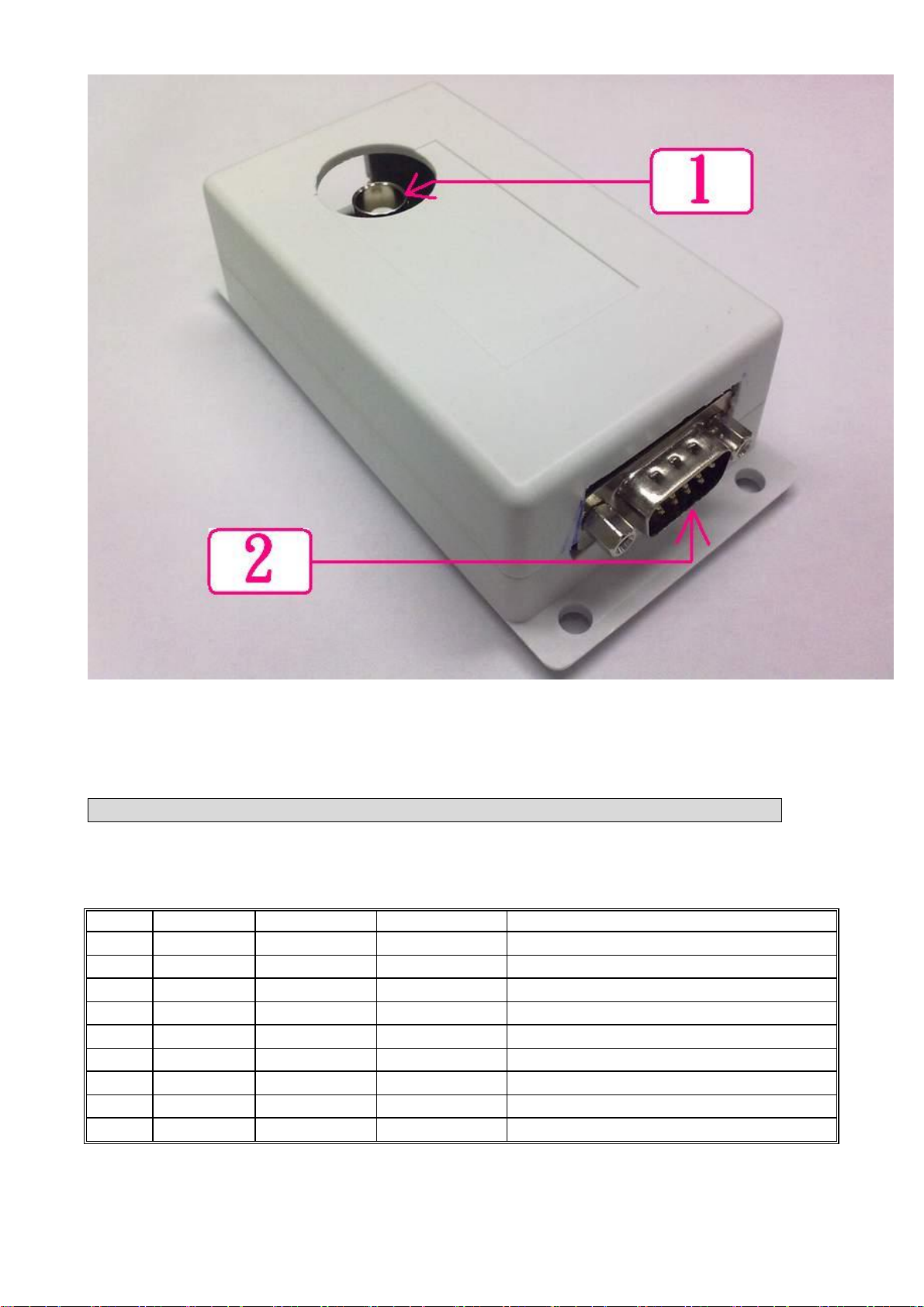
EXTERNAL CONNECTIONS
PIN
FUNCTION
TYPE
RANGE
DESCRIPTION
J2-1
DATA_IN
ANALOGUE
106mV
EXTERNAL MODULATION INPUT
J2-2
DATA_OUT
ANALOGUE
250~350mV
RECEIVER AF OUTPUT
J2-3
PTT
INPUT
0V/+5V
TRANSMIT ENABLE
J2-4
GND
GND
0V
GND
J2-5
B+
V+
+13.8V
POWER SUPPLY
J2-6
CDS
OUTPUT
OPEN/SHORT
RF CARRIER DETECT
J2-7
NC
J2-8
PGM_DATA
INPUT
0V/NC
PROGRAMMER DATA INPUT
J2-9
PGM_ENB
INPUT
0V/5V
PROGRAMMING ENABLE
1. -
50Ω BNC SOCKET
2. - 9 WAY 〝 D 〞TYPE PLUG(J2)
2. CONNECTIONS AND OPERATION
D-TYPE INTERCONNECTIONS
PAGE3
Page 5
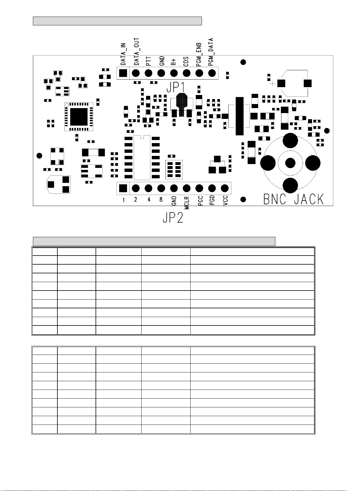
U4(52-7880LC2) CONNECTIONS
PIN
FUNCTION
TYPE
RANGE
DESCRIPTION
JP1-1
DATA_IN
ANALOGUE
106mV
EXTERNAL MODULATION INPUT
JP1-2
DATA_OUT
ANALOGUE
250~350mV
RECEIVER AF OUTPUT
JP1-3
PTT
INPUT
0V/+3.3V
TRANSMIT ENABLE
JP1-4
GND
GND
0V
GND
JP1-5
B+
V+
+6.0V
POWER SUPPLY
JP1-6
CDS
OUTPUT
OPEN/SHORT
RF CARRIER DETECT
JP1-7
PGM_ENB
INPUT
0V/3.3V
PROGRAMMING ENABLE
JP1-8
PGM_DATA
INPUT
0V/NC
PROGRAMMER DATA INPUT
JP1-9
PIN
FUNCTION
TYPE
RANGE
DESCRIPTION
JP2-1
Channel 1
DIGITAL
0V/+3.3V
Channel select pin
JP2-2
Channel 2
DIGITAL
0V/+3.3V
Channel select pin
JP2-3
Channel 4
DIGITAL
0V/+3.3V
Channel select pin
JP2-4
Channel 8
DIGITAL
0V/+3.3V
Channel select pin
JP2-5
GND
GND
0V
GND
JP2-6
MCLR
I
0V/+3.3V
Programming MCU software
JP2-7
PGC
I/O
0V/3.3V
Programming MCU software
JP2-8
PGD
I/O
0V/+3.3V
Programming MCU software
JP2-9
VCC
3.3V
3.3V
VCC
CONNECTIONS AND OPERATION
PAGE4
Page 6

3. CIRCUIT DESCRIPTION
TRANSMITTER
The transmitter is comprised of:
• Audio frequency connections from JP1 pin 1
• Frequency Synthesizer
• Transmitter
Audio frequency connections
In the TX path , audio signal can be send into the chip RDA1846 through AC coupling capacitors.
Frequency synthesizer circuit
Produces the RF carrier frequency for the transmitter during transmit and the local oscillator
frequency for the receiver. The frequency synthesizer circuit is comprised of:
Synthesizer
The U1 (RDA1846) generates the local oscillator and transmitter signal . all building blocks are
fully integrated without any external components. Frequency can be programmed through the serial
interface by the MCU (U3)
26 MHZ TCXO
X1 is VCTCXO, which provide stable oscillator of 26 MHZ to U1.
Frequency adjustment is provided by VR1.
With data received from the EEPROM (U3) the frequency synthesizer circuit controls and
DC REGULATOR
The DC Regulator U4, converts the +6.0 V to a 3.3 V supply . This is used to provide the MCU and U1.
PAGE5
Page 7
RF LPF
ANTENNA
SWITCH
Power Control
Transmitter
The transmitter comprises:
PA Buffer PA Module
Amp
Buffer
When the radio is in transmit mode the U1 is generated RF signal pass to the buffer/pre-amplifier Q1
and Q2 associated components.
PA module
The Q2 output signal is passed to Q3 via a matching network consisting of Inductor L5 , L15 and C32
and C34. Q3 is power amplifier .
Low pass filter
The amplified RF signal is passed through the stripline coupler and is fed to the
harmonic low pass filter, comprising L11, L12, L17 and C46 , C47, C48 and C58 and then to the
antenna connector (J1).
Antenna Switch
When transmitting, the diodes D3 are forward biased, the RF pass to the antenna.
D4 is shorted to ground which makes L13 look open circuit (1/4 wave
tuned stub). This prevents the TX signal from passing to the receiver stage.
PAGE6
Page 8

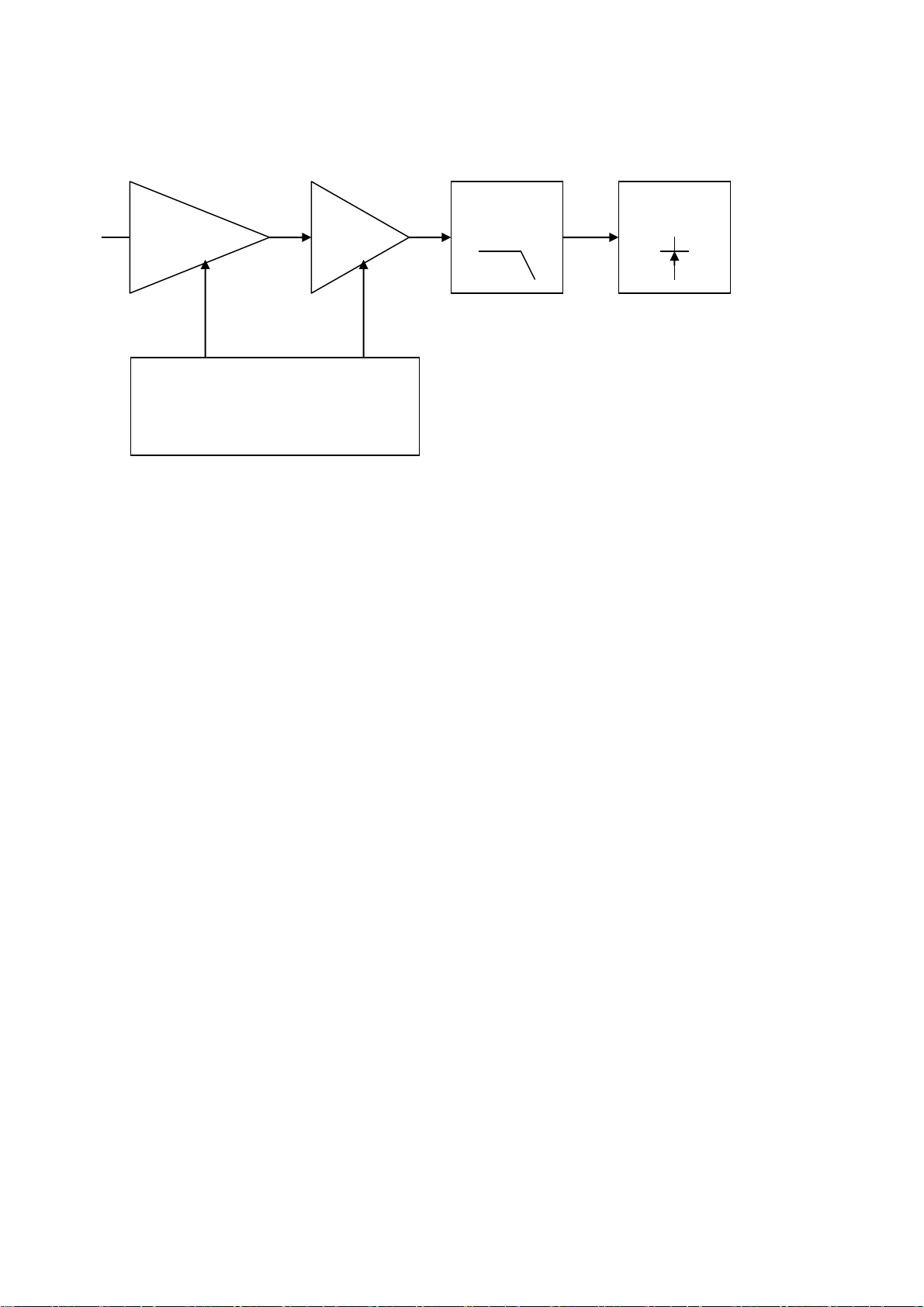
Receiver
The receiver comprises:
Antenna Switch
In receive, the diode D4 are reverse biased. L212 is now in circuit, passing
the signal from the antenna to the U1 LNA input.
. In the RX path , the voice signal after demodulation is sent to the internal DAC which can directly drive
a 32 ohm resistance loading through AC coupling.
Carrier Detect
A Carrier Detect ( MUTE DETECT ) output is available on pin 6 of JP1 .
When noise is present, the voltage at pin 26 of U1 is LOW. The squelch trigger
output is open, It’s make pin 6 of JP1 open state.
When no noise is
This make pin 6 of JP1 short state.
Microcontroller
The PIC16F630 microcontroller IC controls the programmable features and frequency synthesizer
Data.
Programming Mode
The programming mode allows the user to retrieve or program TX/RX frequencies,
when pin 9 of J1 is set to ground. Programming mode will Inhibit ,
Serial communications can then be made in order to read/program the on- board
EEPROM ( U3 )which contains radio- specific data.
EEPROM
Relevant channel information, such as Rx/ Tx frequencies, is stored in the EEPROM( U3)
which is built in PIC16F630. This information may be programmed and erased via the test fixture.
The EEPROM has 1024 (8x128) capacity and is written serially.
present, the
voltage at pin 26 of U1 is HI voltage.
Power supply circuit
The data radio is supplied with a nominal + 6.0V dc power supply input from external
equipment which is filtered using C56. This supply is converted into 3.3V
voltage levels on the board using the regulator U4 and associated components .
This +3.3V line is fed to the CPU circuit.
PAGE7
Page 9

4. PERFORMANCE TEST AND ALIGNMENT
The alignment and performance test procedures assume the use of the following equipment.
Discrete test equipment
Volt Meter Spectrum Analyser and notch filter(option)
RF Power Meter. Coupler (20dB isolation)
DC Power Supply, 0-15V 2A min Distortion Meter
Oscilloscope, 20 MHz dual beam
RF Frequency Counter,
100 kHz - 600 MHz
AF Signal Generator 0 – 20 kHz
RF Signal Generator
SINAD Meter
Modulation Meter
Audio Power Meter
PAGE8
Page 10

5. TEST EQUIPMENT CONFIGURATION.
123.45678
RF Signal Generator
Watt Meter with
20dB Attenuator
Audio Generator
Modulation Meter
SINAD Meter OSCILLOSCOPE
RADIO
VOLT Meter
Spectrum Analyzer
DC Power Supply
Frequency Counter
Test Box
Test Equipment Configuration
PAGE9
Page 11

6. TRANSMITTER PERFORMANCE TESTS
Power Output
1. Set the power supply voltage to 6.0V dc. and monitor the voltage during transmit.
2. Switch data radio TX and check and record the output power. The nominal output
power is adjustable between 2 to 3W .
3. Set the PTT switch to OFF .
Peak Deviation
1. Connect the oscilloscope to the output of the modulation meter.
2. Set the AF signal generator to 1000 Hz at 106mV and connect to DATA _IN
Line ( pin 1 of JP1 )
3. Switch data radio to TX and observe the oscilloscope display to check that the 1000Hz
tone is a sine wave and deviation is about 3.5KHZ.
4. Using the AF signal generator, sweep from 100 Hz to 3 kHz and record the peak
deviation.
5. Check the peak deviation for appropriate channel spacing as follows:
For 12.5 kHz channel spacing, Peak deviation is not greater than 2.5 kHz.
For 20 kHz channel spacing, Peak deviation is not greater than 4 kHz.
For 25 kHz channel spacing, Peak deviation is not greater than 5 kHz.
Spectrum Test
It may be necessary to notch the fundamental signal during this test.
1. Connect a spectrum analyser and RF power meter to the antenna socket.
2. Switch data radio to TX. Observe the output spectrum on the spectrum analyser.
3. Adjust notch filter to minimise the carrier. All spurious and harmonics signals
should be below- 36 dBm up to 1 GHz and below –30 dBm between 1 and 4 GHz.
4. Switch off the data radio transmit control.
Receiver Performance Tests
Sensitivity
The SINAD performance test may be used to test the sensitivity of the receiver.
1. Connect the RF signal generator to the data radio BNC antenna connector.
2. Set the RF signal generator to the receive frequency .
3. Connect the leads of the SINAD meter between 0 V and pin 2 on JP1.
4. Set the deviation to 60﹪of the peak system deviation.
5. Set the AF generator to 1 kHz.
6. Adjust the RF signal generator level until the SINAD Meter reads 12 dB.
7. Check that the signal generator RF level is less than 0.35uV pd (-116dBm ).
PAGE10
Page 12

Transmitter Alignment
Automatic Power Adjustment
Transmit periods longer than 3 minutes are to be avoided.
1. Switch to data radio to TX.
2. make the transmit power between 2 to 3W.
3. Switch the data radio to transmitter OFF.
Frequency accuracy
1. Whilst transmitting, measure the transmit frequency using the RF frequency counter.
2. Adjust VR1 so that frequency is as close as possible to the exact required transmit
frequency. Ideally it should be within 100 Hz at room temperature.
Receiver Alignment
Important note:Before setting up the receiver it is important to check the frequency
accuracy alignment is correct as described in the transmitter alignment section.
RF tuning
1. Connect an RF signal generator and SINAD voltmeter.
2. Set the RF signal generator to the receive channel frequency and set to 60﹪deviation.
3. Set the AF signal to 1 kHz.
4. Set the RF level to 1 mV pd (- 47.0 dBm )
5. Check pin2 of JP1 maximum AF output about 250mVto 350mV and lowest distortion,
the distortion normally less than 5﹪.
6. Check for an RF voltage signal level of 0.35uV pd (- 116dBm)and a SINAD meter
Reading greater than 12 dB.
Squelch⁄Carrier Detect Adjustment
1. Set the RF signal generator to the receiver frequency with 60﹪deviation. Set the AF
Signal to 1 kHz
2. Set RF input level to give -112 dBm.
3. Check pin 6 of JP1 changes state from “HIGH” to “LOW”.
4. Reduce RF input level to –120dBm and check that CDS line goes HIGH . Switch
off the RF generator and disconnect the test equipment.
PAGE11
Page 13

Modulation Deviation Adjustment
1. Connect a power meter, modulation meter and oscilloscope to radio.
2. The radio should be programmed to contain a channel with a frequency in the middle
the band of interest with an RF power setting of 2 W.
3. Switch the data radio ON.
4. Inject a 106mVrms SINE wave signal at a frequency of 1000Hz into pin 1 of JP1,
Set the data radio to TX Observe the oscilloscope display to check that the 1000Hz tone
is a sine wave and set deviation is 3.5KHZ.
5. Using the AF signal generator, sweep from 100 Hz to 3 kHz and record the peak
deviation.
Check the peak deviation for appropriate channel spacing as follows:
12.5 kHz channel spacing<= 2.5 kHz dev
20 kHz channel spacing<= 4 kHz dev
25 kHz channel spacing<= 5 kHz dev
6. Switch to RX.
PAGE12
Page 14

7.PARTS LIST
U4(
52-7880LC2)
Revision:
Bill Of Materials January 19, 2011 15:53:17
Item Quantity Reference Part
_________________________________________________________________
1 12 C1,C8,C13,C15,C16,C17, 470P
C18,C24,C25,C28,C35,C44
2 9 C2,C6,C7,C33,C37,C53,C54, 102P
C56,C63
3 6 C3,C31,C34,C43,C51,C62 5P
4 2 C4,C5 104P/X7R/0603
5 4 C9,C11,C12,C61 104P
6 1 C14 47P
7 3 C22,C46,C48 10P
8 1 C23 33P
9 3 C26,C32,C57 22P
10 2 C27,C47 15P
11 2 C36,C52 NU
12 2 C38,C45 100P
13 1 C41 103P
14 1 C42 9P
15 1 C55 47U/16V/EC/SMT
PAGE13
Page 15

U4(52-7880LC2)
Revision:
Bill Of Materials January 19, 2011 15:53:17
Item Quantity Reference Part
_________________________________________________________________
16 1 C58 6P
17 1 D1 RLS4148
18 2 D3,D4 RLS135
19 1 J1 BNC
20 1 JP1 PCB PLUG 8PIN/2.54mm
21 1 JP2 PCB PLUG 9PIN/2.54mm
22 1 L1 12NH/CHIP
23 2 L2,L13 27NH/CHIP
24 1 L3 6.8NH/CHIP
25 2 L4,L6 22NH/COIL/0805
PAGE14
Page 16

U4(52-7880LC2)
Revision:
Bill Of Materials January 19, 2011 15:53:17
Item Quantity Reference Part
_________________________________________________________________
26 2 L5,L15 5.6NH/CHIP
27 2 L7,L14 4.7NH/COIL/0603
28 1 L8 220NH/CHIP/0603
29 2 L11,L12 12NH/COIL/0603
30 1 L17 18NH/COIL/0603
31 1 Q1 HSC5262
32 1 Q2 RQA0004PXDQS
33 1 Q3 2SK3476
34 1 Q4 DTC114EE
35 1 Q7 UMC4N
36 6 R1,R4,R15,R21,R24,R27 10K
37 4 R2,R3,R5,R16 2K7
38 1 R13 330R
39 1 R17 220R
40 2 R18,R23 18K
41 3 R22,R25,R26 100R
PAGE15
Page 17

U4(52-7880LC2)
C1 C3
CAP7343
CAPACITOR TANT 10UF 25V 20%
C2
CAP
CAP0805 CERM .1UF 10% 50V X7R
D1 D2
DIODE_SMB_400V
RECTIFIER GPP 400V 1A SMB
D3 D4
DIODE-SOD80
DIODE SWITCH 100V 150MA
F1
FUSE_PTC_THROUGHH
OLE
PTC FUSE - THROUGH HOLE
J2
DB9_HORIZ_MALE
---
R2 R3
RES0603
0603 SURFACE MOUNT RESISTOR
U1
7806-TO220_HORIZONT
AL
POSITIVE VOLTAGE REGULATOR; FIXED +12.0
VOLTS 1A
U4
HERMES_RDA1846
---
Revision:
Bill Of Materials January 19, 2011 15:53:17
Item Quantity Reference Part
_________________________________________________________________
42 1 R28 470K
43 1 RP1 10K*4 SMT
44 1 U1 RDA1846
45 1 U2 ELM7S32
46 1 U3 PIC16F630/SOIC/SMT
47 1 U4 UTC UR132L-3.3V-3
48 1 VR1 47KB/SMT
49 1 X1 26MHZ/TCXO
50 1 SHIELD
52-7880LC2B BASE_BOARD partlist
PAGE16
Page 18

8. PROGRAMMER INSTRUCTION
Welcome to PC Programmer.
Please Read this file, before you first use the software.
TABLE OF CONTENTS
1. Brief introduction
2. Before Installing
3. Install PC Programmer
4. INSTRUCTIONS
5. UnInstall PC Programmer
1. Brief introduction
Welcome to PC Programmer. This program is designed to be used with the
Interface Adapter.
The following equipment will be needed to program the Device:
A. A computer to install this program with at least 2 MB available space
in hard disk and a 9-pin male RS-232 serial port.
B. Win 95,Win 98,Win ME or Win 2000 Operation System.
C. Part of the Programming Kit
1) An interface Adapter.
2) A CD disk with the program, PC Programmer files
2. Before Installing
Before You Run Setup, make sure that your computer meets the minimum
requirements mentioned above, and read the Readme file(this file).
NOTE: If you firstly install PC Programmer in you system, the setup may
update some system files on your computer , so you may run the
setup again after your system be updated. Please follow the
installation instruction on the screen.
3. Install
TO install PC Programmer on your computer
1)Insert the CD.
2)Run Setup.exe
3)Follow the installation instruction on the screen.
Important: You cannot simply copy files from the CD to your hard disk
and run PC Programmer . You must use the Setup program,
which decompresses and installs the files in the appropriate
directories. PAGE 17
Page 19

4. INSTRUCTIONS
4.1 Connection
4.2 Start up PC Programmer
4.3 Edit Configuration
4.3.1 Open/Recall/Upload Configuration file
4.3.2 Edit Channel data
4.3.3 Set Option item
4.3.4 (Block)Cut/Copy/Delete/Paste
4.3.5 Auto-Frequency edit
4.3.6 Save a Configuration to disk
4.3.7 Download Configuration to device
4.3.8 Print a Configuration
4.4 Exit PC Programmer
4.1 Connection
1.Connect one side of Interface Adapter to the computer's serial port.
Never care the port number, the PC Programmer will locate it
automatically.
2.Connect the other side of Interface Adapter to the Device's 9-pin
male RS-232 port.
3.Connect power supply to device and LED will be light. The device will into
PC_programming mode automatically, please see the picture of below.
PAGE 18
Page 20

4.2 Start up PC Programmer
1.Select 'Start', choose 'Programs', click on the '*** Serial PC
Programmer' program.
2.When HD Serial PC Programmer is started, a main form will be shown
after a greeting form.
3.There has a menu bar at the top of the main form, and a message box
at the bottom.
NOTE:The program is menu driven for all pertinent commands. All the
commands can be accessed by either key board or the left mouse
button.
Access keys mainly used are:
'Tab' or 'Arrow' to move focus(or cursor)
'Enter' to active a focused command
4.3 Edit Configuration
4.3.1 Open/Upload Configuration file
To edit the configuration, please either
1)Recall an Existing Configuration by click on the 'Open' item in
the File Menu, select the configuration file by click on or input
its name then press 'Enter' key.
OR 2)Upload configuration data from a device by click on 'Upload' item
in the Device menu. to a Configuration window .
Different Model's device Configuration can be opened and edited.
There are two fields in each Configuration window: system data
and Channel data.
OR 3)Open an existing Configuration by click on the 'OPEN' item in the
File Menu. A pop up window will be shown, select a file by arrow
key or mouse then click 'OK'.
4.3.2 Edit Channel data
1)Set focus to the Channel data field by move the mouse pointer.
2)Select a particular channel number to be edited by either the
arrow key or click on it.
3)Pop up input window by either press 'Enter' key or double click
on the selected channel number.
4)Use computer's cursor keys, Tab key, Enter key, arrow key or
mouse to renew the channel data.
5)Click 'OK' button on the input window to accept the change or
'Cancel' to not change, and return back to Configuration Window.
PAGE 19
Page 21

4.3.3 Edit Option item
1)To Edit Channel Option, Select a particular channel number in
the Option View Window by either the arrow key or click on it,
then Pop up the input window for Channel Option, 'Enter' key or
double click on the selected channel number.
2)To Edit System Option, Pop up input window for System Option,
click "SYSTEM" in the 'OPTION' menu.
3)To Edit Advanced Option, Pop up input window for Advanced Option,
click "ADVANCED OPTION" in the 'OPTION' menu.
4Use computer's cursor keys, Tab key, Enter key, arrow key or
mouse to renew the Option Item.
5)Click 'OK' button on the input window to accept the change or
'CANCEL' to not change, and return back to Configuration Window.
4.3.4 (Block)Cut/Copy/Delete/Paste
To select a block of channel data as source by either
1)Select start channel by arrow key, then while press 'Shift' key
select end channel number by arrow key.
2)Click on start channel, then while press 'Shift' key click on
end channel number
3)Press the left mouse button on start channel then move the mouse
until reach the end channel number, release left mouse button.
A)To Cut selected (block) Channel(s) either press 'Ctrl'+'X'or
click 'CUT' item in Edit menu.
B)To Copy selected (block) Channel(s) either press 'Ctrl'+'C'or
click 'COPY' item in Edit menu.
C)To Delete selected (block) Channel(s) either press 'Del(Delete)'
key or click on 'DELETE' item in Edit menu.
After Cut or Copy, the data can be pasted to where you want.
D)To Paste , select a channel as the start number of target , then
either press 'Ctrl'+'V' or click on 'PASTE' item in Edit menu.
NOTE: Paste operation allows you to export data to any Configuration
window opened.
4.3.5 Auto-Frequency edit
This feature provide you with a quick Frequency set function.
To use this command after either
1)Click 'EDIT' Menu
2)Click on 'AUTOFREQ' item in 'EDIT' menu to pop up a input window.
3)Use computer's cursor keys, Tab key, Enter key, arrow key or mouse
to set data.
PAGE 20
Page 22

4)Click 'OK' button on the input window to accept the change or
'CANCEL' to not change, and return back to Configuration Window.
4.3.6 Save a Configuration to disk
1)Different configuration can be saved to disk.
2)Click on 'SAVE' item in 'FILE' Menu will overwrite an existing
configuration file on your disk by current configuration.
3)Select 'SAVE AS' from 'FILE' Menu will save the current
configuration by a name as you prefer.
4.3.7 Download to device
To Download current Configuration to device, select 'DOWNLOAD' from
sub menu under 'DEVICE' menu.
4.3.8 Print a Configuration
Click on 'PRINT' item in 'FILE' Menu will send current Configuration
to printer.
4.4 Exit PC Programmer
To Exit PC Programmer,click on 'EXIT' item in 'FILE' Menu.
5. UnInstall PC Programmer
To uninstall PC Programmer from your hard disk, select 'Start'
, choose 'Settings', click on the 'Control Panel', then find 'Add/Remove
Programs' icon from the pop up window then double click on it, then find
'*** Serial PC Programmer' from application list and click on it, then click
on 'Add/Remove' button under application list, then follow the
instructions on your screen.
PAGE 21
Page 23

Federal Communication Commission Interference Statement
This equipment has been tested and found to comply with the limits for a Class B
digital device, pursuant to Part 15 of the FCC Rules. These limits are designed to
provide reasonable protection against harmful interference in a residential installation.
This equipment generates, uses and can radiate radio frequency energy and, if not
installed and used in accordance with the instructions, may cause harmful interference
to radio communications. However, there is no guarantee that interference will not
occur in a particular installation. If this equipment does cause harmful interference to
radio or television reception, which can be determined by turning the equipment off
and on, the user is encouraged to try to correct the interference by one of the
following measures:
. Reorient or relocate the receiving antenna.
. Increase the separation between the equipment and receiver.
. Connect the equipment into an outlet on a circuit different from that to which the
receiver is connected.
. Consult the dealer or an experienced radio/TV technician for help.
FCC Caution: To assure continued compliance, any changes or modifications not
expressly approved by the party responsible for compliance could void the user's
authority to operate this equipment. (Example - use only shielded interface cables
when connecting to computer or peripheral devices).
This device complies with Part 15 of the FCC Rules and IC RSS-119. Operation is
subject to the following two conditions: (1) This device may not cause harmful
interference, and (2) this device must accept any interference received, including
interference that may cause undesired operation
The antenna of the product, under normal use condition is at least 0.52 m away from
the body of the user. Warning statement to the user for keeping at least 0.52 m
separation distance and the prohibition of operating to a person has been printed on
the user's manual. So, this product under normal use is located on electromagnetic far
field between the human body.
 Loading...