

Page 1

AES
t
IntelliNe
AES Corporation
285 Newbury Street
Peabody,MA 01960-1315 USA
Phone 978-535-7310
Fax 978-535-7313
SERVICE MANUAL
MODEL 7088-UE
Rev 1.0 July 10,2007
Page 2

TABLE OF CONTENS
1.SPECIFICATION
2.CONNECTIONS AND OPERATION
3.PERFORMANCE TEST AND ALIGNMENT
4.TEST EQUIPMENT CONFIGURATION
5.TRANSMITTER PERFORMANCE TEST
6.TROUBLESHOOTING
7.CIRCUIT DESCRIPTION
8.PROGAMMER INSTRUCTION
9.PARTS LIST
10.PRINT CIRCUIT BOARD LAYOUT
11.COMPONENT PLACEMENT
12.BLOCK DIAGRAM
Page 3

1.SPECIFICATION
GENERAL SPECIFICATIONS
POWER SOURCE………………………………………………+13.8VD.C.nominal(+10.8 to +15.6V)
TEMPERATURE RANGE
STORAGE ………………………………………………80℃ maximum -40℃ min.
25℃ nominal
OPERATING……………………………………………60℃ maximum -20℃ min.
ANTENNA IMPEDANCE………………………………………50Ω
FREQUENCY CONTROL……………………………………………PLL SYNTHESISER
FREQUENCY OF OPERATION……………………………………400MHZ-480MHZ
FREQUENCY TOLERANCE AND STABILITY…………………±5PPM
HIGH HUMIDITY……………………………………………………90%
CHANNEL CAPABILITY……………………………………………1
NOMINAL DIMENSIONS …………………………………………134mm(L)X60mm(W)X20mm(H)
WEIGHT ……………………………………………………………190g
RADIO DATA TRANSCEIVER NOMINAL PERFORMANCE
PERFORMANCE SPECIFICATIONS……………………………ETSI 300-113
RF OUTPUT POWER………………………………………………5W PROGRAMMABLE
MODULATION TYPE………………………………………………FM
INTERMEDIATE FREQUENICES………………………………21.7MHZ
450KHZ
CHANNEL SPACING……………………………………………12.5KHZ,25KHZ
TRANSMIT ATTACK TIME………………………………………<25mS
CURRENT CONSUMPTION
TRANSMIT……………………………………………1800mA@5W,
RECEIVE………………………………………………85mA
Page 4
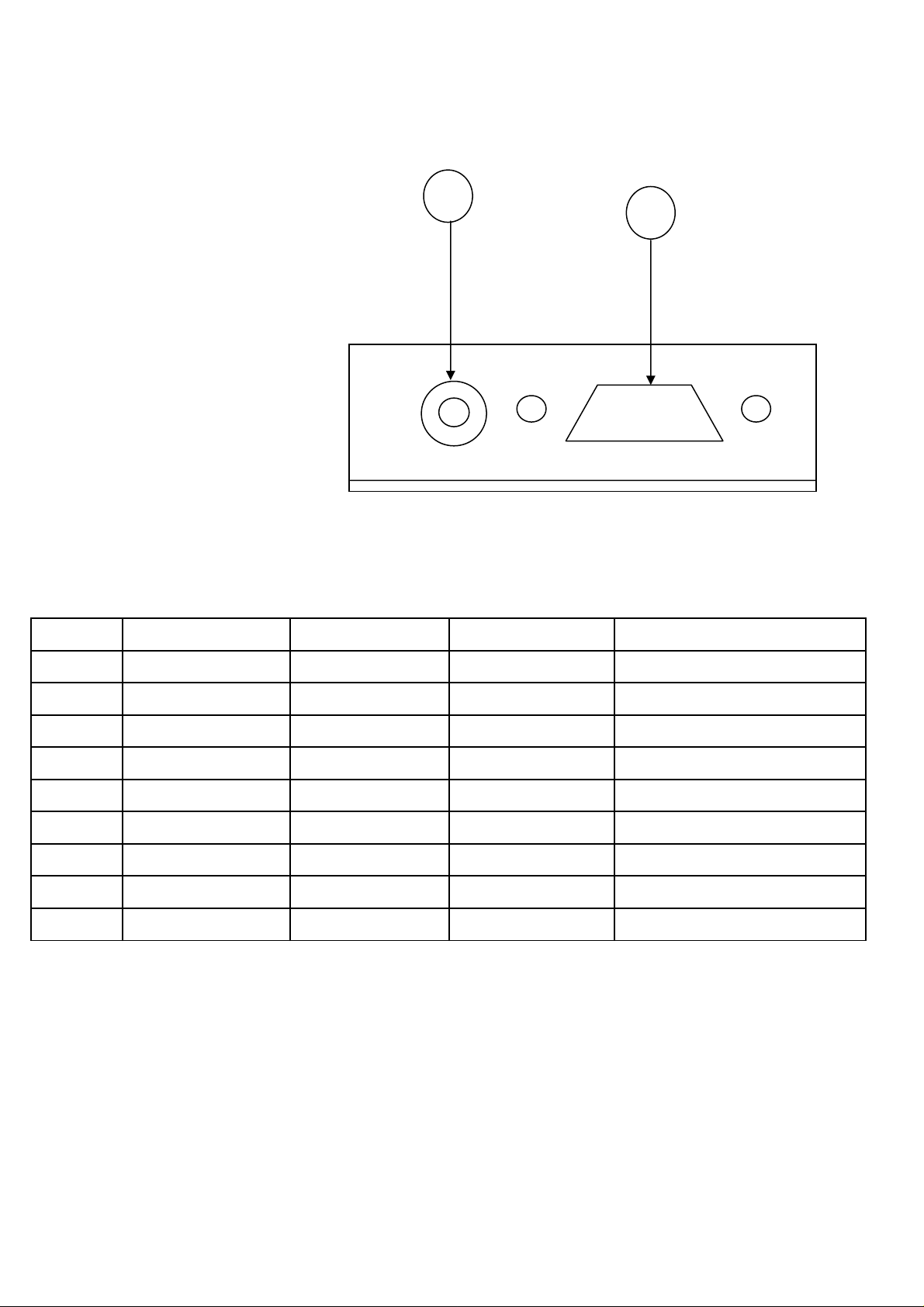
2.CONNECTIONS AND OPERATION
T
EXTERNAL CONNECTIIONS
1-50Ω BNC SOCKET
2-9 WAY "D" TYPE PLUG(D_SUB)
D-TYPE INTERCONNECTIONS
PIN
FUNCTION
TYPE
1
2
RANGE DESCRIPTION
D_SUB-1 ANALOGUE 100Mv-2.5VP-P
D_SUB-2 ANALOGUE
D_SUB-3
D_SUB-4
D_SUB-5
D_SUB-6
D_SUB-7
D_SUB-8
D_SUB-9
DATA_IN
DATA_OUT
PTT
GND 0V
B+
CDS
NC
PGM_DATA
PGM_ENB
GND
V+
OUTPUT
NC
INPUT
INPUT
1VP-P
0V/+5V
+13.8V
OPEN/SHORT
NC
0V/NC
EXTERNAL MODULATION INPU
RECEIVER AF OUTPUT
TRANSMIT ENABLEINPUT
GND
POWER SUPPLY
RF CARRIER DETECT
NC
PROGRAMMER DATA INPUT
PROGRAMMING ENABLE0V/5V
Page 5

3.PERFORMANCE TEST AND ALIGNMENT
t
The alignment and performance test procedures assume the use of the following equipmen
Discrete test equipment
Volt Meter Spectrum Analyser and notch filter(option)
RF Power Meter. Coupler(20dB isolation)
DC Power Supply,0-15V 2A min
Oscilloscope,20MHz dual beam
RF Frequency Counter,
100KHz-600MHz
AF Signal Generator 0-20KHz
RF Signal Generator
SINAD Meter
Modulation Meter
Audio Power Meter
Warning:
This device complies with the following of RF energy exposure standards and guidelines:
* United States Federal Communications Commission, Code of Federal Regulations;47CFR
part 2 sub-part J
* American National Standards Institute (ANSI)/Institute of Electrical and Electronic
Engineers (IEEE) C95. 1-1992
* Institute of Electrical and Electronic Engineers (IEEE) C95. 1-1999 Edition
Please keep 40cm distance away from the antenna.
Only antenna which gain lower than 1.0 can be conntected to the transmitter
4.TEST EQUIPMENT CONFIGURATION
RF Signal Generator
Watt Meter with
20dB Attenuator
Page 6
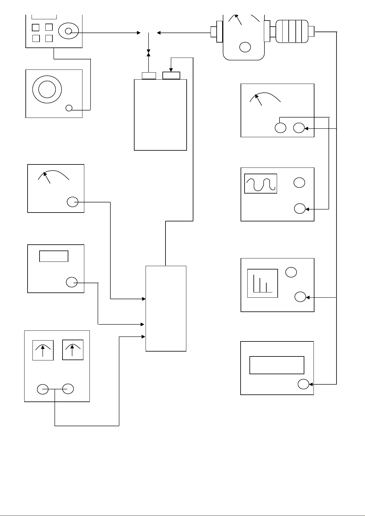
20dB Attenuator
Audio Generator
Modulation Meter
SINAD Meter
VOLT Meter
DC Power Supply
RADIO
OSCILLOSCOPE
Spectrum Analyzer
Frequency Counter
Test Box
123.45678
Test Equipment Configuration
5.TRANSMITTER PERFORMANCE TESTS
Power Output
1. Set the power supply voltage to 13.8V dc.and monitor the voltage during transmit.
2. Switch data radio TX and check and record the output power.The nominal output.
Page 7

power is adjustable between 1 and 5W depending on the programming.
3. Set the PTT switch to OFF.
Peak Deviation
1. Connect the oscilloscope to the output of the modulation meter.
2. Set the AF signal generator to 100Hz at 5V peak-to-peak and connect to DATA_IN Line
(pin 1 of D_SUB)
3. Switch data radio to TX and observe the oscilloscope display to check that the 100Hz
tone is a square wave.
4. Using the AF signal generator,sweep from 100Hz to 3KHz and record the peak deviation.
5. Check the peak deviation for appropriate channel spacing as follows:
For 12.5Khz channel spacing,Peak deviation is not greater than 2.5KHz.
For 25KHz channel spacing,Peak deviation is not greater than 5KHz.
Spectrum Test
It may be necessary to notch the fundamental signal during this test.
1. Connect a spectrum analyser and RF power meter to the antenna socket.
2. Switch data radio to TX.Observe the output spectrum on the spectrum analyser.
3. Adjust notch filter to minimise the carrier.All spurious and harmonics signals should
be below-36dBm up to 1GHz and below-30dBm between 1 and 4GHz.
4. Switch off the data radio transmit control.
Receiver Performance Tests
Sensitivity
The SINAD performance test may be used to test the sensitivity of the receiver.
1. Connect the RF signal generator to the data radio BNC antenna connector.
2. Set the RF signal generator to the receive frequency.
3. Connect the leads of the SINAD meter between 0V and pin 2 on D_SUB.
4. Set the deviation to 60% of the peak system deviation.
5. Set the AF generator to 1KHz.
6. Adjust the RF signal generator level until the SINAD Meter reads 12dB.
7. Check that the signal generator RF level is less than -119dBm.
6.TROUBLESHOOTING
The section includes voltage which should assist the engineer to isolate and repair the fault.
Voltage measurements should be made using a high-impedance voltmeter and the values given
Page 8
are with respect to ground.
Careful alignment,using suitable test equipment,and quality interface cables should
ensure that the radio meet their specified performance.
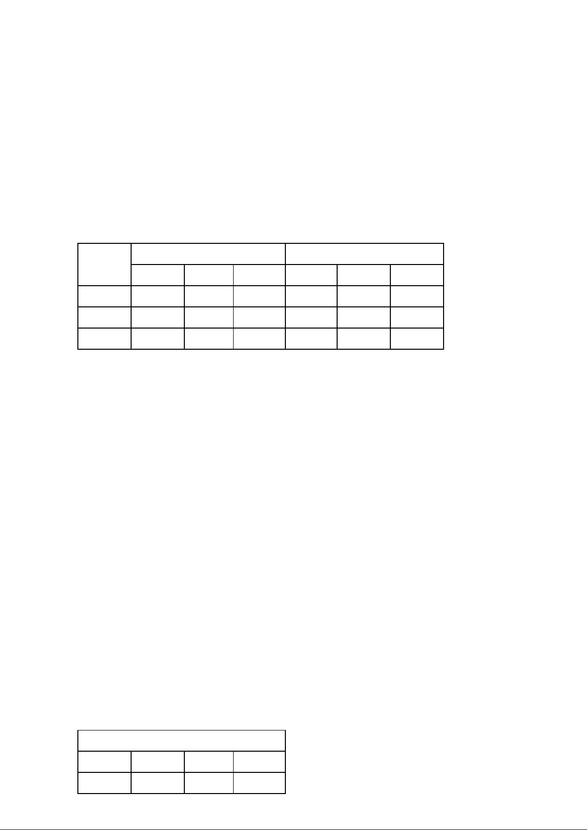
Voltage Charts
Measurement Condition:455.5MHz,13.8V supply,RX Carrier Present.
Transistors.
RX TX
Ref. No.
BCEBC E
T101 0 0 0 0.44 2.5 0
T871 4.96 0 4.97 4.3 2.3 4.9
T323 4.5 4.7 3.8 4.5 4.7 3.8
Integrated Circuits
Pin U621 U401 U240
1 1.35v 4.7v 4.5v
RECEIVER
Page 9
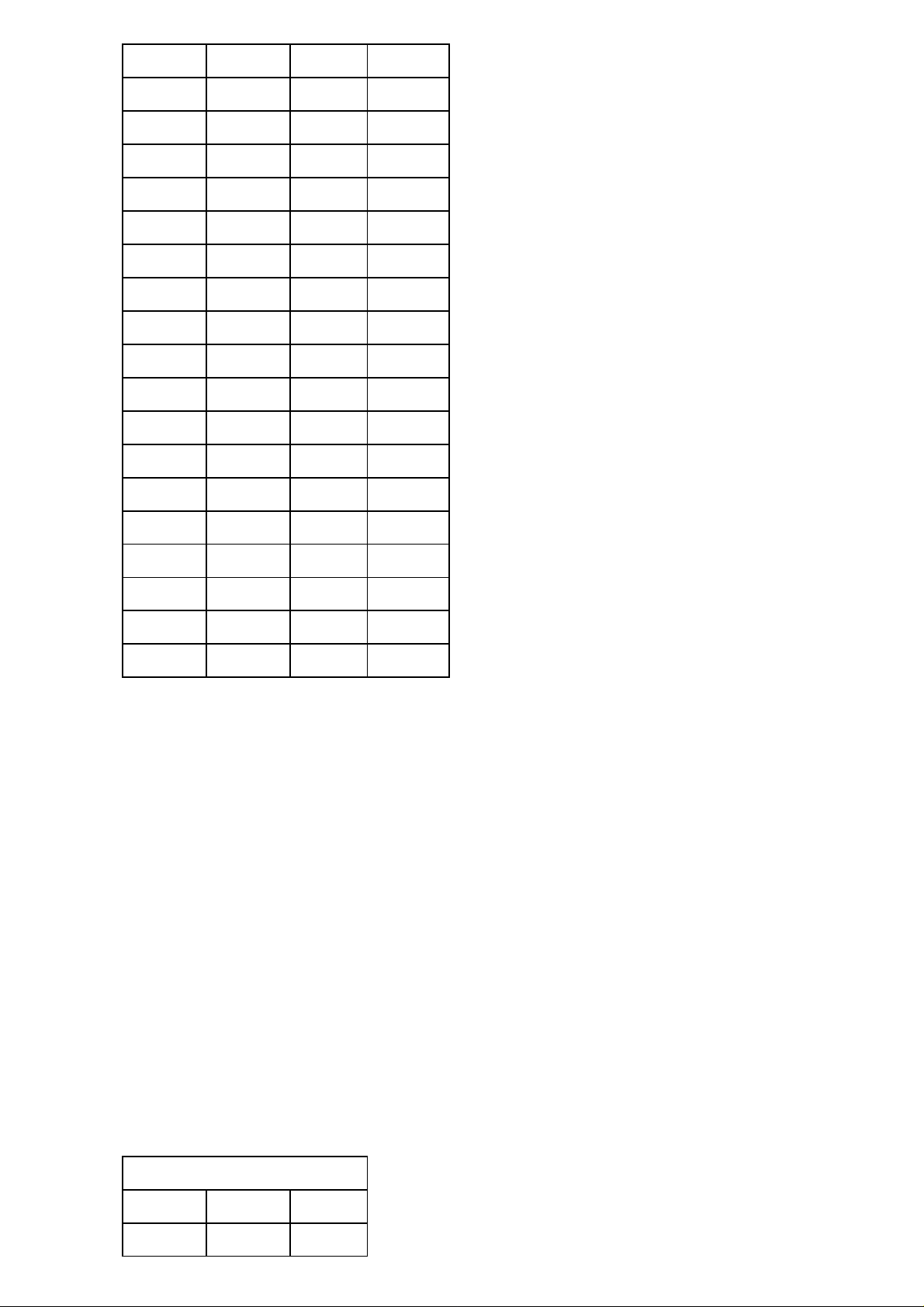
2 0v 4.7v 3.8v
3 0v 2.3v 3.3v
4 0v 0v 4.5v
5 6.9v 1.59v 4.1v
6 13.7v 1.59v 4.1v
7 6.9v 0v 0.6v
8 1.35v 0.65v 0.6v
9 0v 0.9v
10 4.58v 4.5v
11 0v 3.6v
12 4.96v 2.2v
13 4.96v 0v
14 0v 0v
15 0v 0v
16 0v 0.9v
17 0v
18 0v
19 4.6v
20 4.6v
Integrated Circuit Voltages(Receive)
Integrated Circuits
PIN U701 U607
1 0.1v 1.1v
TRANSMIT
Page 10

2 9.1v 1.1v
3 8.9v 1.1v
40v0v
5 0.4v 1.1v
6 0.2v 1.1v
7 12.4v 1.1v
8 13.7v 2.3v
Integrated Circuit Voltages(Transmit)
CIRCUIT DESCRIPTION
TRANSMITTER
The transmitter is comprised of:
Page 11

y Audio amplifier connection from D_SUB pin 1
y Frequency Synthesiser
y Transmitter
y Automatic Power Control
Audio frequency connections
Processed data from the U601A is applied to the VCO via VR521
Frequency synthesiser circuit
With data received from the EEPROM (U911) the frequency synthesiser circuit controls and
Produces the RF carrier frequency for the transmitter during transmit and the local oscillator
frequency for the receiver.The frequency synthesiser circuit is comprised of:
y 12.8MHZ VCTCXO
y Voltage Controlled Oscillator (VCO)
y Charge Pump and Loop Filter
y PLL Frequency Synthesiser
y Dual Modulus Prescaler
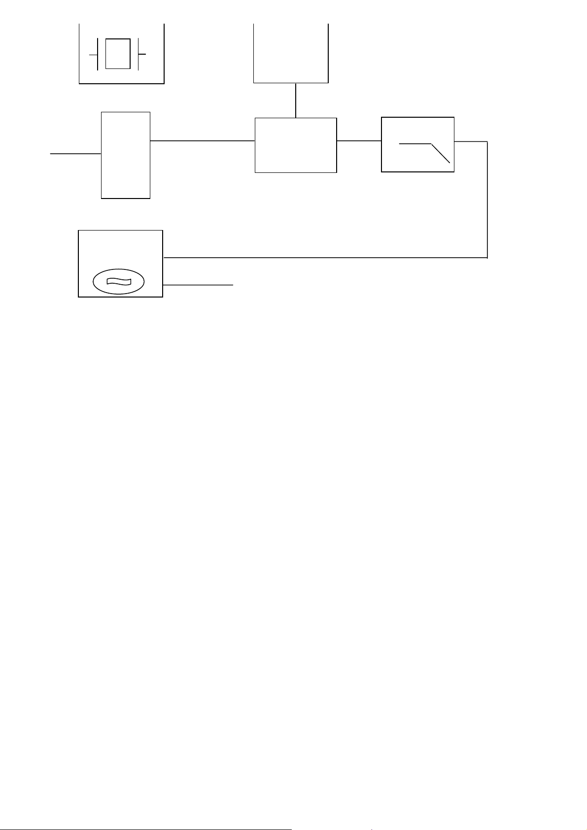
PLL Synthesiser
The PLL synthesiser circuit is common to both the transmitter and receiver,
The synthesiser comprises:
TCXO
Page 12
TCXO
DC
supply
Data
U401
PLL
TX OR RX
VCO
Charge Pump
RF Out
Loop Filter
12.8MHZ VCTCXO
The reference oscillator comprises VR421,CR2(12.8MHZ)and associated resistors and capacitors.
CR2 provides the reference oscillator frequency and the temperature compensation that ensures
that the frequency remains stableacross the temperature range(typically±2.5ppm) CR2 PIN2
is the modulation port for the two port modulation system used in the DATARADIO range of
radios and is DC coupled.The reference oscillator signal direct input to the PLL synthesiser
U401.
Frequency adjustment is provided by VR421
VCO SECTION
The VCO section produces carrier frequencies during transmit and local oscillator
frequencies During receive.
The VCO section contains one VCO and three outputs.One for producing carrier frequencies
during Transmit and one for producing the local oscillator during receive and the other
Output is for PLL IC(U401)Fin.
The VCO section also has Rx and TX powerline filters.
RX and TX power line filters.
Transistor T851、T323 is configured as a 5v power supply ripple filter.The filter reduces the
noise on the carrier and local oscillator signals.
Page 13

The VCO comprises T321,Coil L320,and varactor D303 D302.D303、D302 produces a change in
frequency with a change in DC voltage and is controlled by the tuning voltage signal present at
the cathode.The local oscillator programmable dividers.DATA is received by U401 at pin 12 from
pin 13 of U401.
The RF signal at the collector of T321 is applied to an amplifier/buffer T322.The amplified Signal
from T322 passes to the prescaler,U401 pin5.The RF signal at the collector of T321 also Drives
the cascode amplifier/buffer formed by T322 and T341.
When D341 is forward biased (TX ON),carrier frequencies at the collector of T341 pass to the
Power amplifier and harmonic filter.When D342 is forward biased (RX),local oscillator
Frequencies at the collector of T341 pass to the first mixer (T202).
PLL IC
The reference frequency from the VCTCXO,at 12.8 MHZ,is connected to pin 8 of U401(LMX2332
ATM)The appropriate VCO is connected to pin 13.
REFDIV divides the 12.8 MHZ to produce a reference frequency (Fr) of 5 or 6.25 kHz dependent
upon channel spacing selected.VARDIV divides the prescaled VCO frequency to produce a
variable frequency(Fv).Fv and Fr are fed to the phase detector.
Phase detector
When Fv=Fr,the phase detector output (pins 3 and 18,U401)produces narrow negative pulses
And Fv and Fr pulse widths are identical.The signal at pin 3 and 18 is smoothed the loop filter
and applied to the VCO.
Out-of-lock detector
The out-of-lock detector produces a series of logic level pulses when the loop is out of lock at pin
10 of U401.
Charge Pump and Loop Filter
Associated resistors and capacitors form the charge pump and loop Filter.The phase detector
output from U401 pins 3 by the charge pump to Produce a 0 to 5v tuning voltage signal.
Page 14
The signal is filtered by the loop filter (R403,E402 and E403)to remove any residual reference
Frequency harmonics from the signal.After filtering the signal is applied to the voltage controlled
Oscillator module.
Dual modulus prescaler
The prescaler divides the VCO frequency by 64 or 65.
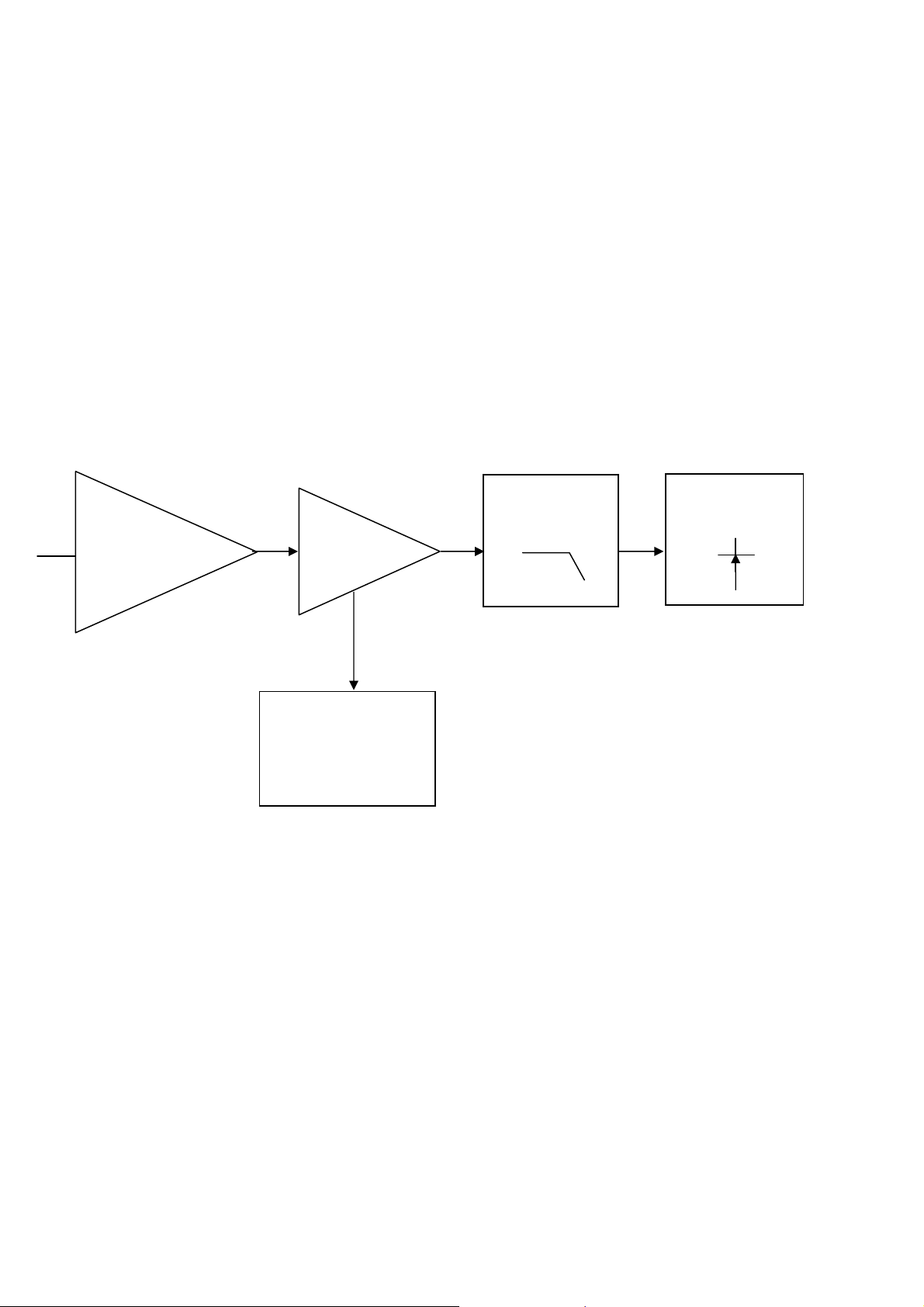
Transmitter
The transmitter comprises:
VCO Buffer
Amp
PA Module
RF LPF
ANTENNA
SWITCH
Automatic
Power Control
Buffer
When the radio is in transmit mode the diode D341 is forward biases enabling the modulated
RF signal from the VCO to pass to the buffer/pre-amplifier T101 and T102、T105 and associated
components.
Page 15

The output signal is passed from T105 to T107 via a matching network consisting of Inductor
L119 and C119.
RF power Amplifier
The signal is then amplified for transmission by T107,which is a RF power amplifier.
Low pass filter
The amplified RF signal is passed through the CAP coupler and is fed to the harmonic low pass
filter,comprising L112、L113、L114、L118、C147、C149、C150、C151、C154、C155 and then
to the antenna connector(ANT).
Antenna Switch
When transmitting,the diodes D101 is forward biased,allowing the RF to pass to the antenna.
D102 is shorted to ground which makes L110 look open circuit(1/4 wave tuned stub).This
prevents the TX signal from passing to the receiver stage.
Automatic power control(APC)circuits
The automatic power control contains the U701 transistors T701 and T702.
Receiver
The receiver comprises:
ANTENNA
SWITCH
Rx
VCO
Front End
Amp
First Mixer
IF Filter
Page 16
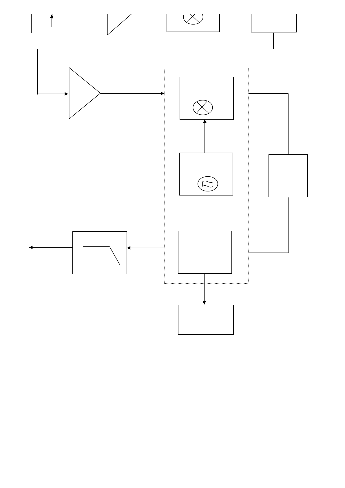
IF Amp
Second
Mixer
Local
Oscillator
IF
Filter
Data Out
Audio Filter
FM
LimiterDiscnminato
Squelch
Circuit
r
Antenna Switch
In receive,the diode D101 and D102 are reverse biased.L110 is now in circuit,passing the signal
from the antenna to the front end without signal loss.
Front End
The receiver signal is routed to T201.It passes through the band pass filter consisting of L204、
L202、L203 to T202.
Diode D103 serves as protection from RF overload from nearby transmitters.
Page 17

The input signal is conpled to the base of T201 which serves as an RF amplifier.
The output of T201 is then coupled to a second bandpass filter consisting of C211 to C212,L206
L207.
The output of the T201,is then coupled to the double-balanced mixer T202.
The receiver front end module is factory pre-tuned and requires no adjustment.
Repair is effected by replacement of the entire module.
First Mixer
T202,2-pole crystal filters FL230 and FL231 and T215 form the First Mixer and First IF Filter.
The difference frequency of 21.7 MHz is taken from T202 and is filtered by the crystal filters
FL230 and FL231.The tuned circuits R230 and R235 and associated components provide
matching of the crystal filters to ensure a good pass-band response and selectivity.
The IF signal is amplified by T215 and passed to the FM Detector IC.
Second mixer,Second IF,FM detector
The output of the IF amplifier is fed into the narrowband FM IF Integrated Circuit,U240
(TA31136F).This is a single conversion FM receiver which contains the second mixer,second IF
amplifier,and FM detector.
Crystal CR240,connected to pin 1 of U240,determines the second local oscillator frequency.
In this case the crystal has a frequency of 21.25MHz.The first IF signal is applied to the mixer
and resultant frequency of 450KHz,is the difference between the IF signal and second local
oscillator.
The 450KHz IF signal is output from pin 3 and is applied to a 450KHz band-pass filter.
The output of FL240 is passed via pin 5 to a high gain IF amplifier coupled to the adjustable
quadrature detector TR240.Any detected signal is produced at pin 9 of U240 and applied to the
Page 18

Receiver Audio Circuit and the Mute(Squelch)Circuit.
RSSI Circuit
Any noise signal is amplified by U240 internal noise amplifier.Signal is applied to pin12 of U240
The squelch trigger output(pin 14,U240)is applied to the pin 6 of D_SUB.
When noise is present,the voltage at pin 12 of U240 is exceeds 1V.The squelch trigger output is
0V(logic 0)It's make pin 6 of D_SUB open state.
When no noise is present,the voltage at pin 12 of U240 is less than 1V and pin 14 of U240
IS AT 5v(logic 1).This make pin 6 of U240 short state.
Carrier Detect
A Carrier Detect(MUTE DETECT)output is available on pin 6 of D_SUB.
AF Output Low Pass Filter
A low pass filter formed by C631 and R632 removes any extraneous 450KHz energy from the AF
output of the FM receiver chip (pin 9 of U240).
The filtered signal is passed to pin 2 of D_SUB.
Microcontroller
The EM78P451AQ microcontroller IC controls the programmable features and frequency
synthesizer Data.
Programming Mode
The programming mode allows the user to retrieve of program TX/RX frequencies,HI/LO power
Setting and channel spacing,when pin 9 of D_SUB is set to ground.Programming mode will
Inhibit,Serial communications can then be made in order to read/program the on-board
EEPROM(U911)which contains radio-specific data.
EEPROM
Relevant channel information,such as Rx/Tx frequencies,is stored in the EEPROM(U911)which
is a 24LC08.This information may be programmed and erased via the D-type socket.
Page 19

Power supply circuit
The data radio is supplied with a nominal +13.8V dc power supply input from external
equipment which is filtered using C805,L801 and C804.
Tuning up procedure
Transmitter Alignment
Automatic Power Adjustment
Transmit periods longer than 3 minutes are to be avoided.
1. Switch to data radio to TX.
2. Select High power setting.
3. Record the transmit power set.
4. Switch the data radio to transmitter OFF.
Page 20

Frequency accuracy
1. Whilst transmitting,measure the transmit frequency using the RF frequency counter.
2. On the VCTCXO PCB,adjust trimmer resistor VR421 so that frequency is as close as
possiable to the exact required transmit frequency.Ideally it should be within 100Hz
at room temperature.
Receiver Alignment
Important note:Before setting up the receiver it is important to check the frequency
accuracy alignment is correct as described in the transmitter alignment section.
RF tuning
1. Connect an RF signal generator and SINAD voltmeter.
2. Set the RF signal generator to the receive channel frequency and set to 60% deviation.
3. Set the AF signal to 1KHz.
4. Set the RF level to 1Mv pd(-47.0dBm)
5. Adjust TR240 for a maximum audio output(viewed on oscilloscope).
6. Adjust L203 and L204 for lowest distortion,this is normally less than 3%.
7. Check for an RF voltage signal level of -119dBm and a SINAD meter Reading greater than
12dB.
Repeat steps 7 to 9 as necessary.
Squelch Carrier Detect Adjustment
1. Set the RF signal generator to the receiver frequency with 60% deviation.Set the AF Signal
to 1KHz.
2. Set RF input level to give -114dBm.
3. Adjust VR1 until D_SUB pin 6 changes state from"HIGH"to"LOW".
4. Reduce RF input level to -120dBm and check that CDS line goes HIGH.Switch off the RF
generator and disconnect the test equipment.
Modulation Deviation Adjustment
1. Connect a power meter,modulation meter and oscilloscope to radio.
2. The radio should be programmed to contain a channel with a frequency in the middle the
band of interest with an RF power setting of 1W.
3. Switch the data radio ON.
4. Inject a 1Vrms(3VP-P)SINE wave signal at a frequency of 100Hz into pin 1 of D_SUB
5. Set the data radio to TX
6. Observe the oscilloscope display to check that the 100Hz tone is a square ware by tuning
VR521.
Page 21
7. Whilst observing the oscilloscope,adjust the deviation and balance potentiometers.VR521 to
obtain a good square at the following deviation:
12.5KHz channel spacing<=2.5KHz dev
25KHz channel spacing<=5KHz dev
8. It may be necessary to alternate the adjustment of the two potentiometers.
9. Sweep the signal generator between 100Hz and 3KHz.Record the peak deviation. The peak
deviation should be as above.If necessary adjust the potentiometers to achieve this.
10. Switch to RX.
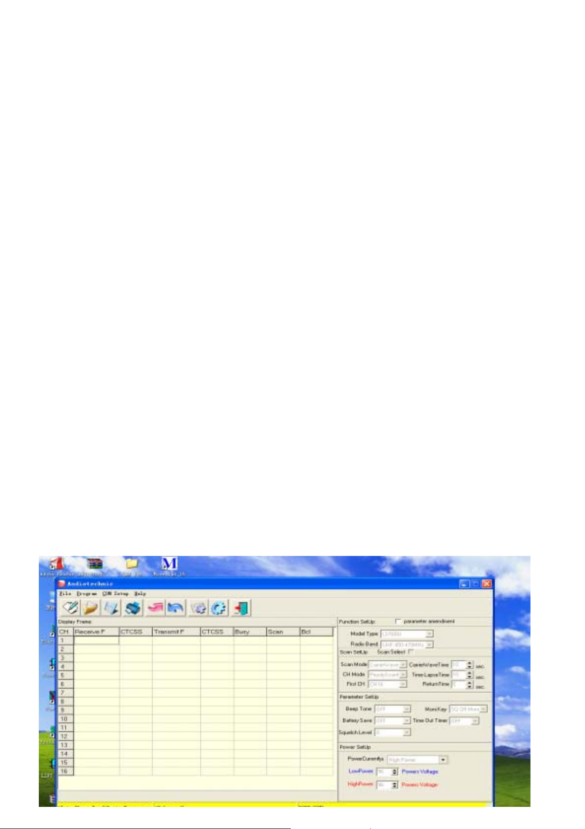
1. Double click AUDIOTECHNIC
PROGRAMMER INSTRUCTION
Page 22
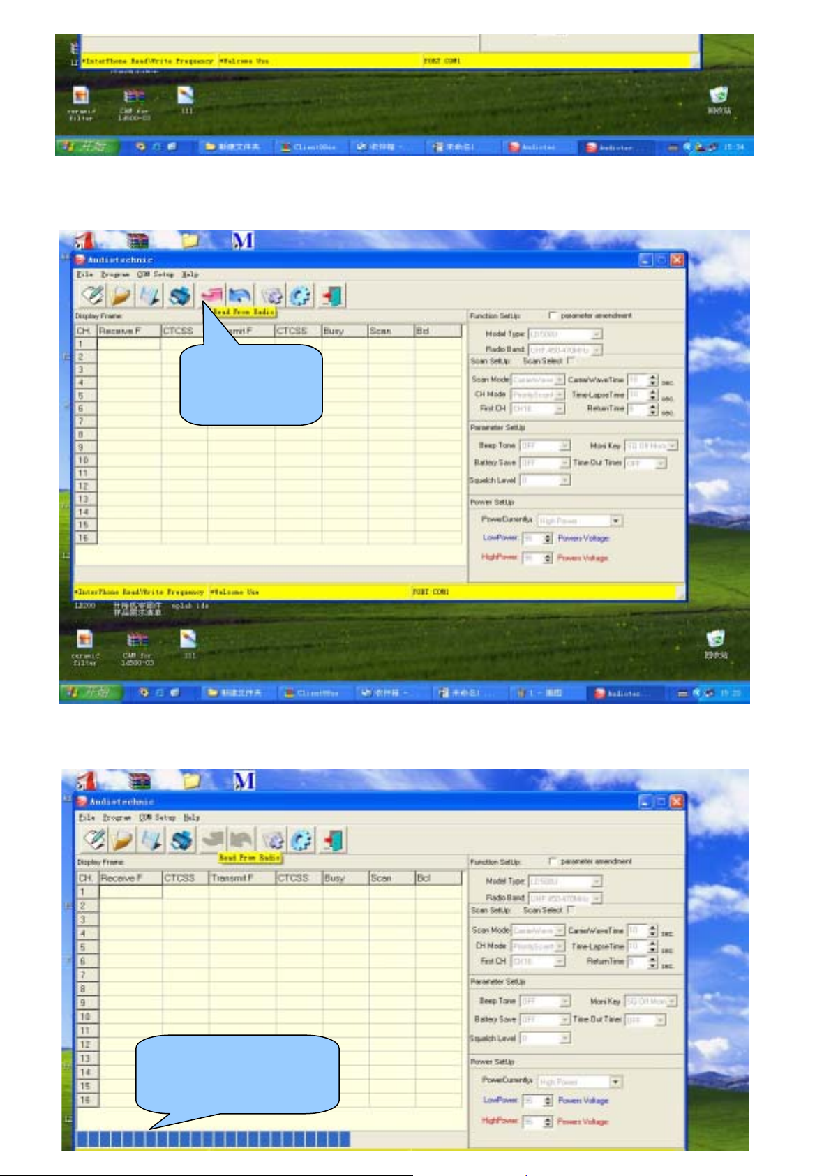
2. press ‘read from radio’ button,then it will read channel data from radio.
'Read from radio'
buttorn
3.next showing as follow
the propress of Reading data
Page 23
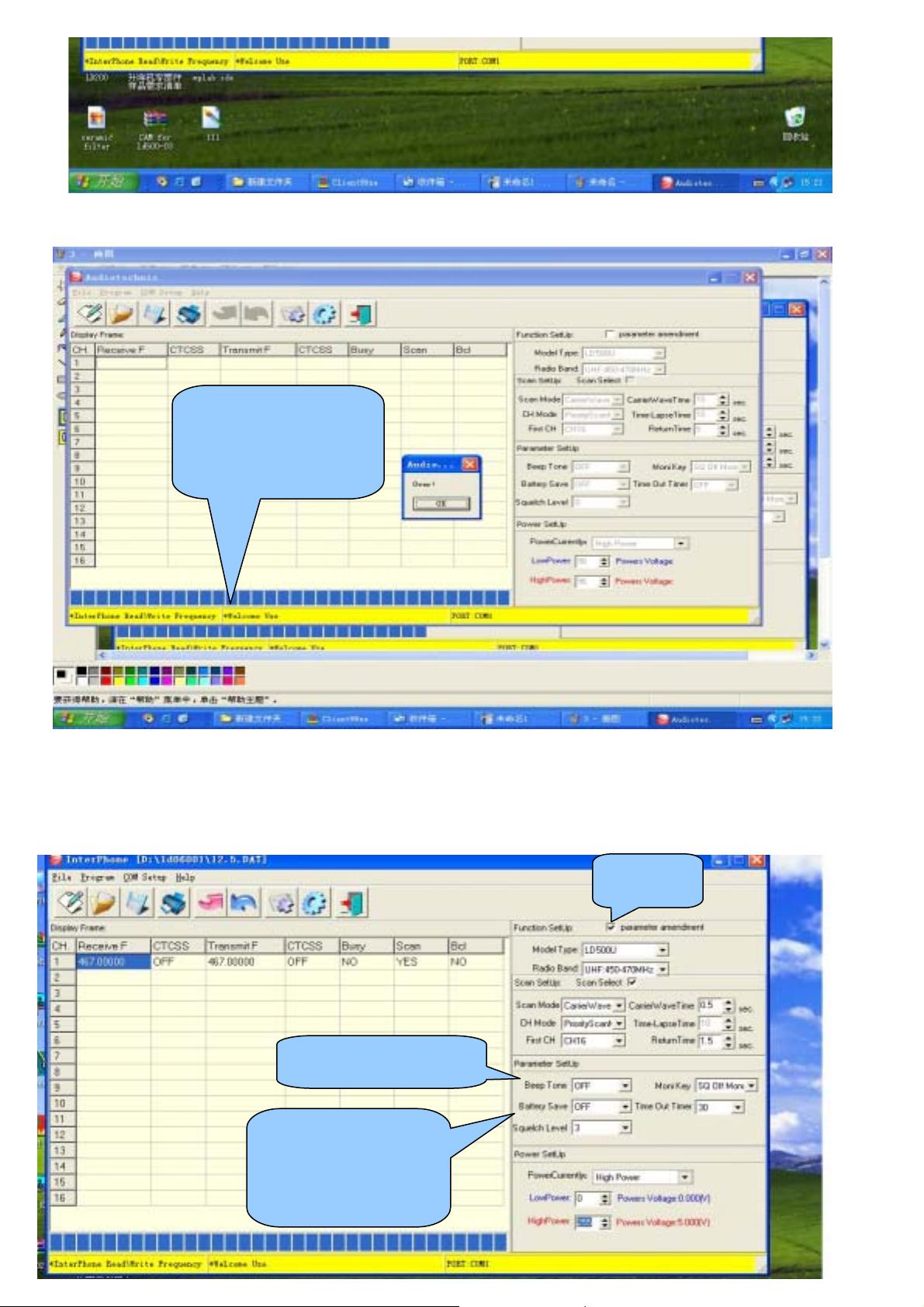
4. finished reading data of radio。
press OK button when
finished reading data of radio
5. then getting into function setup . First , select 'parameter amendment' .
A sound when turn on
Battery power management
Select it
Page 24
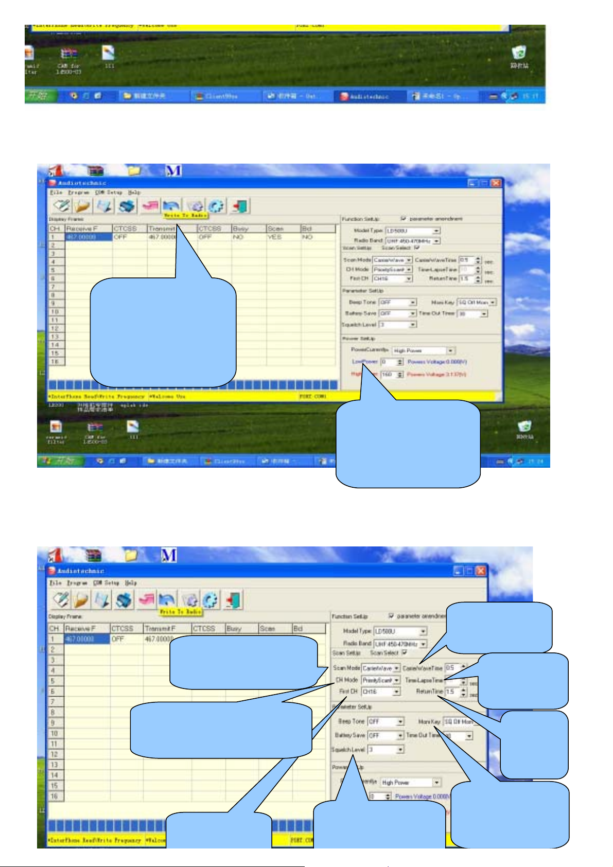
6.If you alter the parameter of 'high power', the output power of radio will be changed, eg. The 255 is the
highest power,the 0 is the lowest power
Press the 'write to radio' button
,then changed parameter will
be saved to radio
selecting 160 in the high
power box ,you can set 2w
output power.
scan mode
1.carrier wave
2.time
channel mode
1.priority channel scan
2.cycscan
first channel
squelch level select
carrier wave time
time-lapse time
scan end
return time
mointor current channel
work status
Page 25
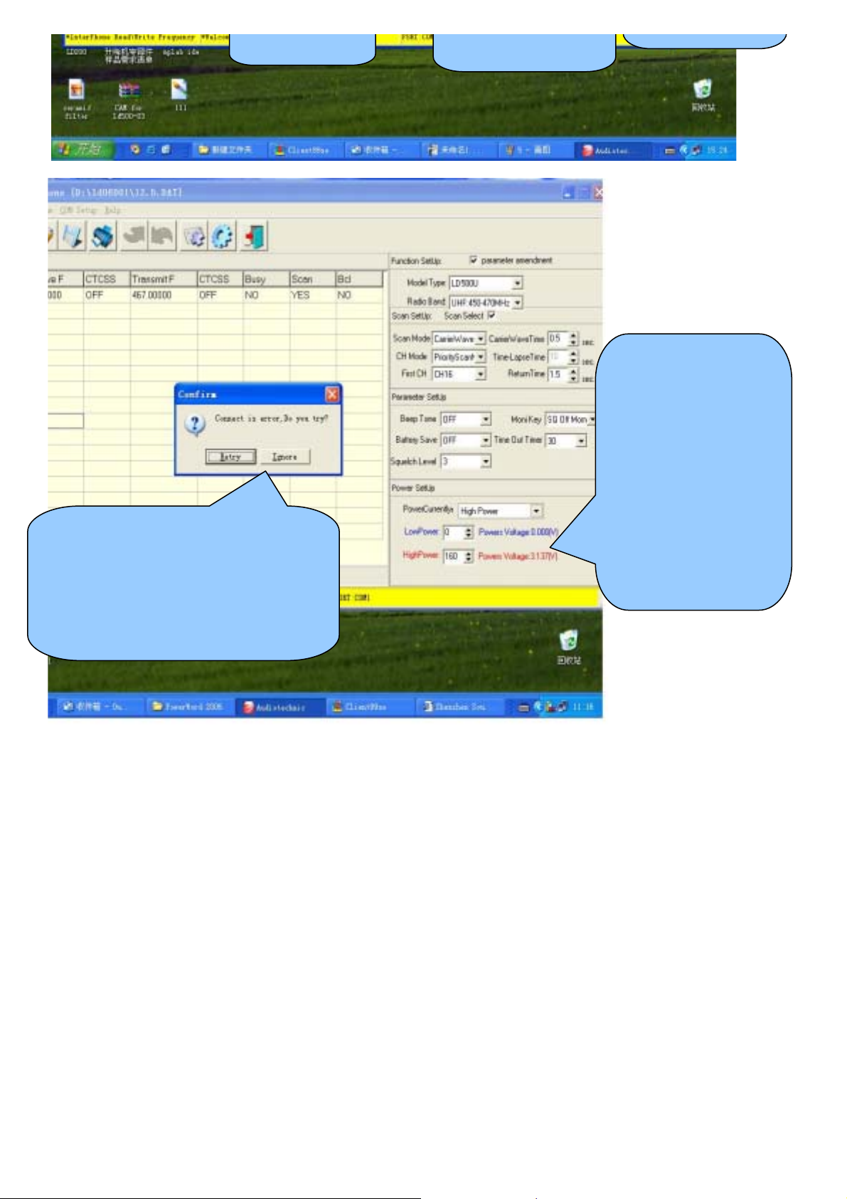
this dialog box will emerge when you
continuous read or write the data of radio
several times,power down the radio and then
reopen it will be ok
only the data in those two box
is different ,can the
highpower and lowpower be
set.for example,if you set 100
in the box of highpoer and
lowpower in the same time
,the computer will default the
hightpower.
 Loading...