

Page 1

HEC
.
L9N-7880
DATA TRANSCEIVERS
PLL SYNTHESIZED
Service Manual
UHF
HERMES ELECTRONICS CO., LTD.
Page 2

1. SPECIFICATION
GENERAL SPECIFICATIONS
POWER SOURCE ………………………………………+5VD.C.
TEMPERATURE RANGE
STORAGE ……………………………………….80℃ maximum -40℃ min.
25℃ nominal
OPERATING …………………………………….60℃ maximum -20℃ min.
ANTENNA IMPEDANCE ………………………………...50Ω
FREQUENCY CONTROL …………………………………...PLL SYNTHESISER
FREQUENCIES OF OPERATION ………………………..402MHZ-470MHZ
FREQUENCY TOLERANCE AND STABILITY …………±2.5PPM
HIGH HUMIDITY ………………………………………….90﹪
CHANNEL CAPABILITY ………………………………….1
NOMINAL DIMENSIONS ………………………………….40 ㎜(L)X30 ㎜(W)X20 ㎜(H)
WEIGHT ……………………………………………………….16g
RADIO DATA TRANSCEIVER NOMINAL PERFORMANCE
PERFORMANCE SPECIFICATIONS ………………………...FCC part 90
RF OUTPUT POWER ……………………………………..0.7w
MODULATION TYPE ……………………………………….FM
INTERMEDIATE FREQUENICES ………………………….307.2 khz
CHANNEL SPACING ………………………………………..25KHZ
TRANSMIT ATTACK TIME …………………………<25 mS
CURRENT CONSUMPTION
TRANSMIT ……………………………….520mA@0.7W
RECEIVE ………………………………..2.5mA
PAGE2
Page 3

14.7456 MHz VCTCXO
An external clock signal from VCTCXO X1 is connect to CC1020 XOSC_Q1 , This VCTCXO is only
5x3.2x1.4(H) mm, and is manufactured with a ceramic base and metal lid to assure very good aging
characteristics and reliability. This device offers an in ±2.5PPM over -30 to +75 Celsius. The VR1 is used
to adjust the frequency is as close as possible to the exact required transmit frequency. Ideally it should be
within 100 Hz at room temperature.
PA module
The U2 is a power amplifier IC as the final RF amplifier in the 400MHz to 480MHz band.
Low pass filter
The amplifier RF signal is through the harmonic low pass filter, comprising L63 to L65 and C62-C66 and
then to the antenna connector J1.
Antenna switch
When transmitting, the diode D61 and D60 are forward biased, allowing the RF to pass to the antenna. D60
is shorted to ground which makes L61 look open circuit (1/4 wave tuned stub ). This prevents the TX signal
from passing to the receiver stage.
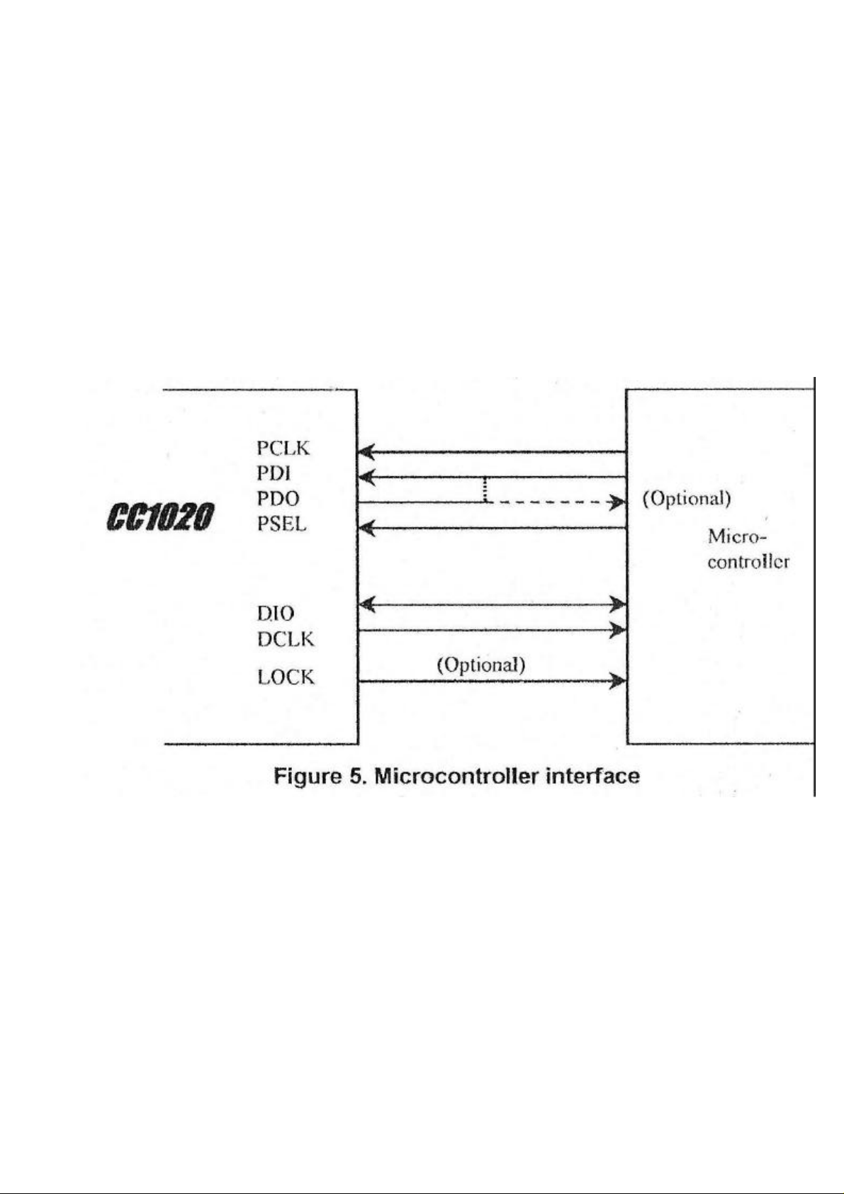
Microcontroller interface
Used in a typical system, CC1020 will interface to a microcontroller. This microcontroller must be able to:
. Program CC1020 into different modes via the 4-wire serial configuration interface (PDI, PDO, PCLK,
and PSEL)
. Interface to the bi-directional synchronous data signal interface (DIO and DCLK)
. Optionally, the microcontroller can do data encoding / decoding
. Optionally, the microcontroller can monitor the LOCK pin for frequency lock status, carrier sense status,
or other status information
. Optionally, the microcontroller can read back digital RSSI value and other status information via 4-wire
serial interface
PAGE6
Page 4
DI, PDO and PCLK are high impedance inputs as long as PSEL is not
Configuration interface
The microcontroller interface is shown in figure 5. The microcontroller uses 3 or 4 I/O pins for the
configuration interface(PDI, PDO, PCLK and PSEL). PDO should be connected to an input at the
microcontroller. PDI, PCLK and PSEL muse be microcontroller outputs. One I/O pin can be saved if PDI
and PDO are connected together and a bi-directional pin is used at the microcontroller.
The microcontroller pins connected to PDI, PDO and PCLK can be used for other purposes when the
configuration interface is not used. P
activated (active low).
PSEL has an internal pull-up resistor and should be left open (tri-stated by the microcontroller) or set to a
high level during power down mode in order to prevent a trickle current flowing in the pull-up.
Signal interface
A bi-directional pin is used for data (DIO) to be transmitted and data received. DCLK providing the data
timing should be connected to a microcontroller input.
As an optional, the data output in receive mode can be made available on a separate pin.
PLL lock signal
Optionally, one microcontroller pin can be used to monitor the lock signal. This signal is at low logic level
when the PLL is in lock. It can also be used for carrier sense and to monitor other internal test signals.
PAGE7
Page 5

4-wire serial configuration interface
line. The seven most significant bits of each data time (A6:0)
bits has been loaded,
CC1020 is configured via a simple 4-wire SPI-compatible (PDI, PDO, PCLK and PSEL). There are 8-bit
configuration register, each addressed by a 7-bit address. A Read/Write bit initiates a read or write
operation. A full configuration of CC1020 requires sending 33 data frames of 16 bits each (7 address bits,
R?W bit and 8 data bits). The time needed for a fu ll configuration depends on the PCLK frequency. When
a PCLK frequency of 10MHz the full configuration is done in less than 53 us. Setting the device in power
down mode requires sending one frame only and will in this case less than 2 us. All registers are also
readable.
In each write-cycle, 16 bits are sent on the PDIare the address-bits. A6 is the MSB (Most Significant Bit) of the address and is sent as the first bit. The
next bit is the R/W bit (high for write, low for read). The 8 data-bits are then transferred (D7:0). During
address and data transfer the PSEL (Program SELect) must be kept low. See Figure 6.
The timing for the programming is also shown in Figure 6 with reference to Table 4. The clocking of the
data on PDI is done on the positive edge of PCLK. When the last bit, D0, of the 8 datathe data word is loaded in the internal configuration register.
The configuration data will be retained during a programmed power-down mode, but not when the
power-supply is turned off. The register can be programmed in any order.
The configuration registers can also be read by the microcontroller via the same configuration interface.
The seven address bits are sent first, then the R/W bit set low to initiate the data read-back. CC1020 then
return the data from the addressed register. PDO is used as the data output and must be configured as an
input by the microcontroller. The PDO is set at the negative edge of PCLK and should be sampled at the
positive edge. The read operation is illustrated in Figure 7.
PAGE8
Page 6

PAGE9
Page 7

Signal Interface
The CC1020 can be used with NRZ (Non-Return-to-Zero) data or Manchester (also known as
bi-phase-level) encoded data.CC1020 can also synchronize the data from the demodulator and provide the
data clock at DCLK. The data format is controlled by the DATA_FORMAT[1:0] bits in the MODEM
register.
CC1020 can be configured for three different data formats:
Synchronous NRZ mode. In transmit mode CC1020 provides the data clock at DCLK, and DIO is used as
data input. Data is clocked into CC1020 at the rising edge of DCLK. The data is modulated at RF without
encoding. In receive mode CC1020 does the synchronization and provides received data clock at DCLK
and data at DIO. The data should be clocked into the interfacing circuit at the rising edge of DCLK. See
Figure 8.
Synchronous Manchester encoded mode. In transmit mode CC1020 provides the data clock at DCLK, and
DIO is used as data input. Data is clocked into CC1020 at the rising edge of DCLK and should be in NRZ
format. The data is modulated at RF with Manchester code. The encoding is done by CC1020. In this mode
the effective bit rate is half the baud rate due to the coding. In receive mode CC1020 does the
synchronization and provides received data clock at DCLK and data at DIO. CC1020 does the decoding
and NRZ data is presented at DIO. The data should be clocked into the interfacing circuit at the rising edge
of DCLK. See figure 9.
In synchronous NRZ or Manchester mode the DCLK signal runs continuously both in RX and TX unless
the DCLK signal is gated with the carrier sense signal or the PLL lock signal.
If SEP_DI_DO = 0 in the INTERFACE register, the DIO pin is the data output in receive mode and data
input in transmit mode.
As an option, the data output can be made available at a separate pin. This is done by setting SEP_DI_DO
= 1 in the INTERFACE register. Then, the LOCK pin will be used as data output in synchronous mode,
overriding other use of the LOCK pin.
Transparent Asynchronous UART mode. In transmit mode DIO is used as data input. The data is modulated
at RF without synchronization or encoding. In receive mode the raw data signal from the demodulator is
sent to the output (DIO). No synchronization or decoding of the signal is done in CC1020 and should be
done by the interfacing circuit.
PAGE10
Page 8

If SEP_DI_DO = 0 in the INTERFACE register, the DIO pin is the data output in receive mode and data
input in transmit mode. The DCLK pin is not active and can be set to a high or low level by
DATA_FORMAT[0].
If SEP_DI_DO = 1 in the INTERFACE register, the DCLK pin is the data output in receive mode and the
DIO pin is the data input in transmit mode. In TX mode the DCLK pin is not active and can be set to a high
or low level by DATA_FORMAT[0]. See Figure 10.
Manchester encoding and decoding
In the synchronous Manchester encoded mode CC1020 uses Manchester coding when modulating the data.
The CC1020 also performs the data decoding and synchronization. The Manchester code is based on
transitions; a “0” is encoded as a low-to-high transition, a “1” is encoded as a high-to-low transition. See
Figure 11.
The Manchester code ensures that the signal has a constant DC component, which is necessary in some
FSK demodulator.
PAGE11
Page 9

PAGE12
Page 10

4. PERFORMANCE TEST AND ALIGNMENT
The alignment and performance test procedures assume the use of the following equipment.
Discrete test equipment
Volt Meter Spectrum Analyser and notch filter(option)
RF Power Meter. Coupler (20dB isolation)
DC Power Supply, 0-10V 1A min
RF Frequency Counter,
100 kHz - 600 MHz
AF Signal Generator 0 – 20 kHz
RF Signal Generator
Modulation Meter
Audio Power Meter
PAGE13
Page 11

Federal Communication Commission Interference Statement
This equipment has been tested and found to comply with the limits for a Class B digital device,
pursuant to Part 15 of the FCC Rules. These limits are designed to provide reasonable
protection against harmful interference in a residential installation. This equipment generates,
uses and can radiate radio frequency energy and, if not installed and used in accordance with
the instructions, may cause harmful interference to radio communications. However, there is no
guarantee that interference will not occur in a particular installation. If this equipment does cause
harmful interference to radio or television reception, which can be determined by turning the
equipment off and on, the user is encouraged to try to correct the interference by one of the
following measures:
- Reorient or relocate the receiving antenna.
- Increase the separation between the equipment and receiver.
- Connect the equipment into an outlet on a circuit different from that to which the receiver is
connected.
- Consult the dealer or an experienced radio/TV technician for help.
FCC Caution: To assure continued compliance, (example - use only shielded interface cables
when connecting to computer or peripheral devices) any changes or modifications not expressly
approved by the party responsible for compliance could void the user's authority to operate this
equipment.
This device complies with Part 15 of the FCC Rules. Operation is subject to the following two
conditions: (1) This device may not cause harmful interference, and (2) this device must accept
any interference received, including interference that may cause undesired operation.
Page 12

This device is intended only for OEM Integrators. The OEM integrator should be
aware of the following important issues.
Labeling of the End Product
The end product integrate this module has to be clearly identified on the label that this
end product contain an FCC approved RF module. The format of such statement
could containTx FCC ID: L9N-7880
Integration Note
a) This module is authorized under limited module approval specified to mobile host
equipment. So, the antenna must be installed such that 20cm is maintained
between the antenna and users.
b) The transmitter module may not be co-located with any other transmitter or
antenna.
As long as the 2 conditions above are met, further transmitter testing will not be
required. However, the OEM integrator is still responsible for testing their
end-product for any additional compliance requirements required with this module
installed (for example, digital device emission, PC peripheral requirements, etc.)
IMPORTANT NOTE:
In the event that these conditions can not be met, then the FCC authorization is
no longer considered valid and the FCC ID can not be used on the final product
(including the transmitter) and obtaining a separate FCC authorization.
 Loading...