

Page 1

AES Corporation does not have a “user’s manual” for this device. The only manual that is available is a
“service manual” because of the intended use and sale of this product. This service manual is provided
below.
Page 2

AES
7085-VE
VHF
SYNTHESISED
DATA TRANSCEIVER
Service Manual
Page 3

40-7085-VE-SM Document Rev A1 10/2003
AES Corporation
285 Newbury Street. Peabody, Massachusetts 01960-1315
Tel (978) 535-7310. Fax (978) 535-7313
Copyright 2003, All rights Reserved
Page 4

TABLE OF CONTENS
1. SPECIFICATION
2. CONNECTIONS AND OPERATION
3. CIRCUIT DESCRIPTION 4-
4. PERFORMANCE TEST AND ALIGNMENT
5. TEST EQUIPMENT CONFIGURATION
6. TRANSMITTER PERFORMANCE TEST
7. TROUBLESHOOTING
8. PROGRAMMER INSTRUCTION
9. PARTS LIST
22-35
17-19
20
13
14-16
2
3
12
12
10. PRINT CIRCUIT BOARD LAYOUT
11. PARTS ASSE MBLY
12. BLOCK DIAGRAM
13. SCHEMATICS DIAGRAM
44-49
50
51
36-43
PAGE 1
Page 5

1. SPECIFICATION
GENERAL SPECIFICATIONS
POWER SOURCE +12VD.C. nominal (+10.8 to +15.6V )
TEMPERATURE RANGE
STORAGE 80ºC maximum -40ºC min.
25ºC nominal
OPERATING 60ºC maximum -20ºC min.
ANTENNA IMPEDANCE 50Ω
FREQUENCY CONTROL PLL SYNTHESISER
FREQUENCIES OF OPERATION 140MHZ - 174MHZ
FREQUENCY TOLERANCE AND STABILITY ±1.5PPM
HIGH HUMIDITY 90%
CHANNEL CAPABILITY 1
NOMINAL DIMENSIONS 134 mm (L) X60 mm (W) X20 mm (H)
WEIGHT 190g
RADIO DATA TRANSCEIVER NOMINAL PERFORMANCE
PERFORMANCE SPECIFICATIONS ETSI 300-113
RF OUTPUT POWER 5W/1W PROGRAMMABLE
MODULATION TYPE FM
INTERMEDIATE FREQUENICES 45 MHZ
455 KHZ
CHANNEL SPACING 12.5 KHZ , 6.25 KHZ (PROGRAMMABLE)
TRANSMIT ATTACK TIME < 25 mS
CURRENT CONSUMPTION
TRANSMIT 1500mA@5W, 800mA@1W
RECEIVE 85mA
PAGE 2
Page 6

2. CONNECTIONS AND OPERATION
EXTERNAL CONNECTIONS
1-
50Ω BNC SOCKET
9 PIN “D” TYPE PLUG (J501)
2-
D-TYPE INTERCONNECTIONS
J501-1 DATA_IN ANALOGUE 100Mv-2.5VP-P EXTERNAL MODULATION INPUT
J501-2 DATA_OUT ANALOGUE 1VP-P RECEIVER AF OUTPUT
J501-3 PTT INPUT 0V/+5V TRANSMIT ENABLE
J501-4 GND GND 0V GND
J501-5 B+ V+ +13.8V POWER SUPPLY
J501-6 CDS OUTPUT OPEN/SHORT RF CARRIER DETECT
J501-7 NC NC NC NC
J501-8
J501-9 PGM_ENB INPUT 0V/5V PROGRAMMING ENABLE
PGM_DATA
INPUT 0V/NC PROGRAMMER DATA INPUT
PAGE 3
Page 7

3. CIRCUIT DESCRIPTION
TRANSMITTER
The transmitter is comprised of:
• Audio amplifier connections from J501 pin 1
• Frequency Synthesizer
• Transmitter
• Automatic Power Control
Audio frequency connections
Processed data from the IC504 is applied to the VCO via P305 and applied to the TCXO
P701
Frequency synthesizer circuit
With data received from the EEPROM (IC502) the frequency synthesizer circuit controls
and Produces the RF carrier frequency for the transmitter during transmit and the local
oscillator frequency for the receiver. The frequency synthesizer circuit is comprised of:
• 12.8 MHZ Tcxo
• Voltage Controlled Oscillator (VCO) module
• Charge Pump and Loop Filter
• PLL Frequency Synthesizer
• Dual Modulus Prescaler
PAGE 4
Page 8
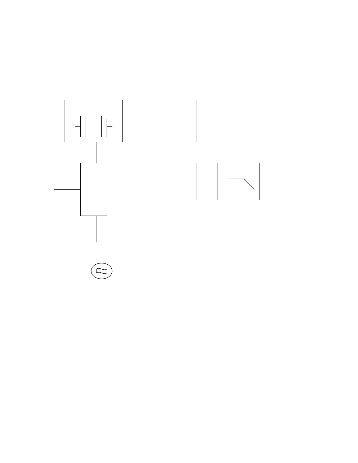
PLL Synthesizer
The PLL synthesizer circuit is common to both the transmitter and receiver.
The synthesizer comprises:
TCXO
DC-DC
Converter
Data
IC1
PLL
Charge Pump
Loop Filter
RF Out
TX OR RX
VCO
Voltage controlled oscillator module (VCO)
The module contains two VCOs. One for producing carrier frequencies during transmit (TX
VCO) and one for producing the local oscillator frequency during receive (RX VCO). The
module also has RX and TX power line filters. Output is for PLL IC(IC1) Fin.
PAGE 5
Page 9

RX and TX power line filters
Transistor Q308 is configured as a 5v power supply ripple filter. The filter reduces the noise
on the carrier and local oscillator signals.
RX
VCO
The RX VCO comprises JFET Q301, coil L301 , and varactor D301 and is configured as a
Colpitts Oscillator . D301 produces a change in frequency with a change in DC voltage and
is controlled by The tuning voltage signal present at the cathode. The local oscillator signal
at the source of Q301 is Applied to the cascode buffer/amplifier formed by Q16 and Q17.The
Local signal is applied to the Mixer when diode D2 is reverse biased and D3 is forward
biased.
TX VCO
The TX VCO comprises JFET Q301,coil L303 , and varactor D302 and D303 and is
configured as A Colpitts oscillator . D302 produces a change in frequency with a change in
DC voltage and is controlled by the tuning voltage signal present at the cathode. The AF
signal at J501 pin 1 is applied to the cathode of D303 to produce FM modulation. When
diode D2 is forward biased and D3 is reversed biased the modulated RF signal at the
collector of Q16 is passed to the power Amplifier and harmonic filter via the cascade
buffer/amplifier (Q21 and Q22).
PLL IC
The reference frequency from the TCXO, at 12.8 MHZ, is connected to pin 1 of IC1 (MB1504)
The appropriate VCO is connected to pin 11.
REFDIV divides the 12.8 MHz to produce a reference frequency (Fr) of 5 or 6. 25 kHz
dependent upon channel spacing selected. VARDIV divides the prescaled VCO frequency to
produce a variable frequency (Fv). Fv and Fr are fed to the phase detector.
Phase detector
When Fv=Fr, the phase detector output (pins 15 and 16,IC1) produces narrow negative
pulses And Fv and Fr pulse widths are identical. When FvFr pin 15 (V) pulses negative with
pin 16 (R) remaining high. When FvFr pin 16 (R) pulses negative with pin 15(V) remaining
high. The signal at pin 15 and 16 is smoothed the loop filter and applied to the VCO.
Out-of-lock detector
T
he out-of-lock detector produces a series of logic level pulses when the
loop is out of lock at pin 7 of IC1.The pulses at pin 7 of IC1 are buffered by
Q6 and then integrated by R17 and C19. The product of the integrating
circuit is fed to IC501 pin 25.
PAGE 6
Page 10
Charge Pump and Loop Filter
Transistors Q2, Q4, Q10, and associated resistors and capacitors form
the charge pump and loop Filter. The phase detector output from IC1
pins 15 and 16 are combined by the charge pump to produce a 0 to
15V tuning voltage signal.
The signal is filtered by the loop filter (R13, C16 and C17) to remove
any residual reference Frequency harmonics from the signal. After
filtering the signal is applied to the voltage controlled Oscillator
module.
DC to DC Converter
The DC-to-DC converter converts the +7.5 V to a 14-16 V supply. This
is used to provide the Tuning voltage for the VCO. A wide voltage
range is required to allow for the wideband operation of the radio.
Q506 to Q508, and associated components, form a 200kHz oscillator.
The output of the oscillator is rectified and filtered by D503, D506,
C548 and C11. The resultant 16VDC is passed to R544 and then
becomes the supply rail for the charge pump.
Dual modulus prescaler
The prescaler divides the VCO frequency by 64 or 65.
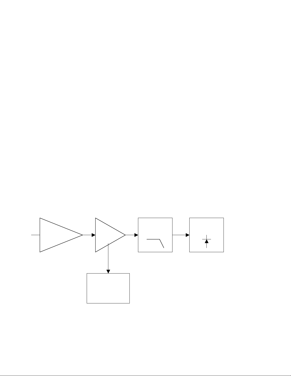
Transmitter
The transmitter comprises:
VCO Buffer PA Module
Amp
Automatic
Power Control
RF LPF
ANTENNA
SWITCH
PAGE 7
Page 11

Buffer
When the radio is in transmit mode the diode D2 is forward biases enabling the modulated RF signal
from the VCO to pass to the buffer/pre-amplifier Q21 and Q22 and associated components.
The output signal is passed from Q22 to IC5 via a matching network consisting of Inductor L7 and
C73.
PA module
The signal is then amplified for transmission by IC5, which is a power amplifier module.
Low pass filter
The amplified RF signal is passed through the stripline coupler and is fed to the harmonic low pass
filter, comprising L12 to L15 and C94-C98 and then to the antenna connector (ANT). The stripline
coupler provides a sample of the RF signal for the automatic power control.
Antenna Switch
When transmitting, the diodes D5 and D6 are forward biased, allowing the RF to pass to the antenna.
D6 is shorted to ground which makes L11 look open circuit (1/4 wave tuned stub). This prevents the
TX signal from passing to the receiver stage.
Automatic power control (APC) circuits
The automatic power control contains the stripline coupler, diode D4, variable resistor RV1, U4A
and transistors Q19 and Q23.
The RF signal present in the coupler is rectified by D4, to produce a DC voltage. This DC voltage is
passed to one input of IC4A, which is a differential amplifier. In transmit mode a DC reference level
for U4A is supplied by the potential divider R34/R35.
The reference level and the detected level from D4 are compared a difference signal is produced. The
difference signal drives Q19, which then drives Q23. Q23 controls the supply voltage to the first
amplifier stage in IC5. This control loop produces a constant power output at the antenna connector
( ANT ).
RV1 is used to adjust the voltage that is fed back from D4 which defines the output RF power level.
PAGE 8
Page 12
Receiver
The receiver comprises:
Front End
Amp
ANTENNA
SWITCH
Rx
VCO
First Mixer
IF Filter
IF Amp
Second
Mixer
Local
Oscillator
Data Out
Audio Filter
FM
Limiter-
Discriminator
IF
Filter
PAGE 9
Squelch
Circuit
Page 13

Antenna Switch
In receive, the diode D5 and D6 are reverse biased. L11 is now in circuit, passing the signal from the
antenna to the front end without signal loss.
Front End
The receiver signal is routed to pin 1 of the RF Front End module. It passes through the band pass
filter consisting of C800 to C808/L800 to L803.
Diode D800 serves as protection from RF overload from nearby transmitters.
The input signal is coupled to the base of Q800, which serves as an RF amplifier.
The output of Q800 is then coupled to a second band pass filter consisting of C814 to C822 / L804 to
L806.
The output of the front end module, pin6, is then coupled to the double-balanced mixer IC8.
The receiver front end module is factory pre-tuned and requires no adjustment.
Repair is effected by replacement of the entire module.
First Mixer
IC8, 2-pole crystal filters XF1 and XF2 and coils L16 and L18 form the First Mixer and First IF
Filter.
IC8 is a self-contained double balanced mixer. The RF signal, from the front end is applied to pin 4
and the VCO local oscillator signal is applied to pin 1.
The difference frequency of 45 MHz is taken from pin 5 and is filtered by the crystal filters XF1 and
XF2. The tuned circuits L16 and L18 and associated components provide matching of the crystal
filters to ensure a good pass-band response and selectivity.
The IF signal is amplified by Q24 and passed to the FM Detector IC.
Second mixer, Second IF, FM detector
The output of the IF amplifier is fed into the narrowband FM IF Integrated Circuit, IC6 (MC3371).
This is a single conversion FM receiver which contains the second mixer, second IF amplifier, and
FM detector.
PAGE 10
Page 14

Crystal X1, connected to pin 1 of IC6, determines the second local oscillator frequency. In this case
the crystal has a frequency of 44.545MHz. The first IF signal is applied to the mixer and resultant
frequency of 455KHz, is the difference between the IF signal and second local oscillator.
The 455KHz IF signal is output from pin 3 and is applied to a 455KHz band-pass filter, CF1 (12.25
kHz channel spacing) or CF2 (6.25 kHz channel spacing). The selection of the filters is
accomplished by diodes D13 (input) and D14 (output) whose bias is controlled by software and
applied to the diodes from pin 21 of IC501.
The output of CF1/CF2 is passed via pin 5 to a high gain IF amplifier coupled to the adjustable
quadrature detector T2 (pin 8). Any detected signal is produced at pin 9 of IC6 and applied to the
Receiver Audio Circuit and the Mute (Squelch) Circuit.
Squelch (MUTE) Circuit
The noise detect circuit in conjunction with IC6 consists of diode D11 and RV2.
Any noise signal is amplified by IC6 internal noise amplifier rectified by D11 .D11 Signal is applied
to pin12 of IC6. The squelch trigger output (pin 14,IC6) is applied to the pin 6 of J501.
When noise is present, the voltage at pin 12 of IC6 is less than 0.7V. The squelch trigger output is
0V(logic 0) It’s make pin 6 of J501 open state.
When no noise is present, the voltage at pin 12 of IC6 exceeds 0.7v and pin 14 of IC6 IS AT
5v(logic 1). This make pin 6 of J501 short state.
Carrier Detect
A Carrier Detect (MUTE DETECT) output is available on pin 6 of J501.
AF Output Low Pass Filter
A low pass filter formed by C134, C135 and R82 removes any extraneous 455kHz energy from the
AF output of the FM receiver chip (pin 9 of IC6).
The filtered signal is passed to pin 2 of J501.
Micro controller
The PIC 16C57 microcontroller IC controls the programmable features and frequency synthesizer
data.
PAGE 11
Page 15

Programming Mode
The programming mode allows the user to retrieve or program TX/RX frequencies, HI/LO power
Setting and channel spacing, when pin 9 of J501 is set to ground. Programming mode will Inhibit,
Serial communications can then be made in order to read/program the on- board EEPROM
( IC502 )which contains radio- specific data.
EEPROM
Relevant channel information, such as RX / TX frequencies, is stored in the EEPROM (IC502)
which is a 93C46. This information may be programmed and erased via the D- type socket. The
EEPROM has 1024 (8x128) capacity and is written serially.
Power supply circuit
The data radio is supplied with a nominal + 13.8V dc power supply input from external equipment
which is filtered using C532 ,L501 and C533.This supply is converted into three separate voltage
levels on the board using the switching transistor Q506 and associated components .
The +13.8Vdc supply and Q506 switching waveform are summed using D503 to supply a boosted
voltage supply, which is regulated at +16V using Zener diode D506. This supply is used as the
supply for the tuning voltage for the VCOs.
The +6V line is regulated by Zener diode D505 and filtered using L503 and C538.This +6V line is
fed to the RF circuit and is regulated to +5V using two regulators on the board.
4. PERFORMANCE TEST AND ALIGNMENT
The alignment and performance test procedures assume the use of the following equipment.
Discrete test equipment
Volt Meter Spectrum Analyzer and notch filter (option)
RF Power Meter. Coupler (20dB isolation)
DC Power Supply, 0-15V 2A min
Oscilloscope, 20 MHz dual beam
RF Frequency Counter,
100 kHz - 600 MHz
AF Signal Generator 0 – 20 kHz
RF Signal Generator
SINAD Meter
Modulation Meter
Audio Power Meter
PAGE 12
Page 16
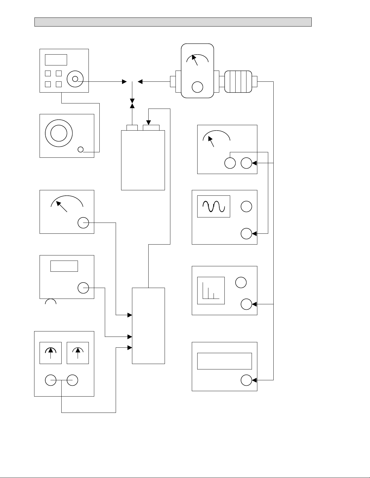
5. TEST EQUIPMENT CONFIGURATION.
RF Signal Generator
Watt Meter with
20dB Attenuator
Audio Generator
Modulation Meter
SINAD Meter OSCILLOSCOPE
RADIO
VOLT Meter
Spectrum Analyzer
DC Power Supply
Frequency Counter
Test Box
123.45678
Test Equipment Configuration PAGE 13
Page 17

6. TRANSMITTER PERFORMANCE TESTS
Power Output
1. Set the power supply voltage to 13.8V DC and monitor the voltage during transmit.
2. Switch data radio TX and check and record the output power. The nominal output power is
adjustable between 1 and 5W depending on the programming.
3. Set the PTT switch to OFF.
Peak Deviation
1. 1. Connect the oscilloscope to the output of the modulation meter.
2. Set the AF signal generator to 100 Hz at 5Vpeak–to-peak and connect to DATA _IN Line (pin 1
of J501)
3. Switch data radio to TX and observe the oscilloscope display to check that the 100Hz tone is a
square wave.
4. Using the AF signal generator, sweep from 100 Hz to 3 kHz and record the peak deviation.
5. Check the peak deviation for appropriate channel spacing as follows:
For 12.5 kHz channel spacing, Peak deviation is not greater than 2.5 kHz.
For 6.25 kHz channel spacing, Peak deviation is not greater than 2 kHz.
Spectrum Test
It may be necessary to notch the fundamental signal during this test.
1. Connect a spectrum analyzer and RF power meter to the antenna socket.
2. Switch data radio to TX. Observe the output spectrum on the spectrum analyzer.
3. Adjust notch filter to minimize the carrier. All spurious and harmonics signals should be below-
36 dBm up to 1 GHz and below –30 dBm between 1 and 4 GHz.
4. Switch off the data radio transmit control.
Receiver Performance Tests
Sensitivity
The SINAD performance test may be used to test the sensitivity of the receiver.
1. Connect the RF signal generator to the data radio BNC antenna connector.
2. Set the RF signal generator to the receive frequency .
3. Connect the leads of the SINAD meter between 0 V and pin 2 on J501.
4. Set the deviation to 60% of the peak system deviation.
5. Set the AF generator to 1 kHz.
6. Adjust the RF signal generator level until the SINAD Meter reads 12 dB.
7. Check that the signal generator RF level is less than 0.35uV pd (-116 dBm).
PAGE 14
Page 18

T ransmitter Alignment
Automatic Power Adjustment
Transmit periods longer than 3 minutes are to be avoided.
1. Switch to data radio to TX.
2. Adjust RV1 to give the appropriate transmit power.
3. Record the transmit power set.
4. Switch the data radio to transmitter OFF.
Frequency accuracy
1. Whilst transmitting, measure the transmit frequency using the RF frequency counter.
2. On the TCXO PCB, adjust trimmer capacitor VC700 so that frequency is as close as possible to
the exact required transmit frequency. Ideally it should be within 100 Hz at room temperature.
Receiver Alignment
Important note: Before setting up the receiver it is important to check the frequency accuracy
alignment is correct as described in the transmitter alignment section.
RF tuning
1. Connect an RF signal generator and SINAD voltmeter.
2. Set the RF signal generator to the receive channel frequency and set to 60deviation.
3. Set the AF signal to 1 kHz.
4. Set the RF level to 1 mV pd (- 47.0 dBm)
5. Adjust T2 for a maximum audio output (viewed on oscilloscope).
6. Adjust L16 and L17 for lowest distortion; this is normally less than 3.
7. Check for an RF voltage signal level of 0.35uV pd (- 116dBm) and a SINAD meter Reading
greater than 12 dB.
Repeat steps 7 to 9 as necessary.
Squelch ⁄ Carrier Detect Adjustment
1. Set the RF signal generator to the receiver frequency with 60deviation. Set the AF
a. Signal to 1 kHz
2. Set RF input level to give -115 dBm.
3. Adjust RV2 until CDS J501 pin 6 changes state from “HIGH” to “LOW”.
4.
Reduce RF input level to –120dBm and check that CDS line goes HIGH . Switch off the RF
generator and disconnect the test equipment.
PAGE 15
Page 19

Modulation Deviation Adjustment
1. Connect a power meter, modulation meter and oscilloscope to radio.
2. The radio should be programmed to contain a channel with a frequency in the middle the band of
interest with an RF power setting of 1 W.
3. Switch the data radio ON.
4. Inject a 1Vrms(3VP-P) SINE wave signal at a frequency of 100Hz into pin 1 of J501
5. Set the data radio to TX
6. Observe the oscilloscope display to check that the 100Hz tone is a square ware by tuning RV502.
7. Whilst observing the oscilloscope, adjust the deviation and balance potentiometers. RV501 and
RV502 to obtain a good square at the following deviation:
12.5 kHz channel spacing <= 2.5 kHz dev
6.25 kHz channel spacing <= 2 kHz dev
8. It may be necessary to alternate the adjustment of the two potentiometers.
9. Sweep the signal generator between 100Hz and 3kHz. Record the peak deviation.
The peak deviation should be as above. If necessary adjust the potentiometers to achieve this.
10. Switch to RX.
PAGE 16
Page 20

7. TROUBLESHOOTING
This section includes voltages, which should assist the engineer to isolate and repair a fault.
Voltage measurements should be made using a high-impedance voltmeter and the values given are with
respect to ground.
Careful alignment, using suitable test equipment, and quality interface cables should ensure that the radio
meet their specified performance.
Voltage Charts
Measurement Condition: 162.8750MHZ, 13.8V supply, RX Carrier Present.
Transistors.
Ref. No.
RX TX
B C E B C E
Q2 15.72 5.67 15.88 15.72 5.33 15.88
Q4 0 5.67 0 0 5.33 0
Q6 4.02 0 4.14 4.02 0 4.14
Q8 0.48 1.96 0 0.48 1.96 0
Q9 4.81 5.02 4.14 4.81 5.02 4.14
Q10 3.77 15.28 3.66 3.77 15.28 3.66
Q11 6.68 0 6.82 0 5.61 6.66
Q12 0 6.68 0 0.72 0 0
Q14 4.63 0 5.03 4.3 4.92 5.02
Q15 0 4.86 5.02 5.02 0 5.02
Q16 2.63 4.98 1.86 2.63 4.98 1.86
Q17 0.89 1.7 0.12 0.89 1.7 0.12
Q18 0 0 0 0 4.76 4.90
Q19 0 13.8 0 1.16 12.8 0.63
Q21 0 0 0 0.43 2.05 0
Q22 0 0 0 2.53 4.72 2.05
Q23 13.72 0 13.8 13.25 4.49 13.8
Q24 0.7 3.94 0 0 0 0
Q25 0.68 0 0 0 7.73 0
Q31 5.0 0 0 5.0 0 0
Q32 5.0 0 0 5.0 0 0
Q33 5.0 0 0 5.0 0 0
Q34 0 0 0 0 0.72 0
Q35 0 0 0 0.72 0 0
Q502 4.38 5.04 5.06 4.38 5.04 5.06
Q503 0.74 0 0 0 5.05 0
Q505 0 4.65 0 0.72 0 0
Q506 13.22 7.5 13.8 13.22 8.24 13.8
Q507 0.11 11.92 0 0.03 10.6 0
Q508 0.57 0.11 0 0.51 0.03 0
Q509 0 0 0 5.0 0 0
Q512 5.0 0 0 0 0 0
PAGE 17
Page 21

Integrated Circuits
RECEIVER
Pin IC1 IC2 IC5 IC6 IC8 IC501 IC502 IC504 IC508 U4
1 1.92 6.82 0 4.25 0 0 0 2.49 5.03 0
2 1.98 0 0 3.65
0 5.05 0 2.48 5.03 0
3 0.48 5.02 0 3.53 0 0 5.05 2.26 0 0
4 4.14 13.8 4.38 0 0 0 5.05 5.05 0
5 0 0 3.34 0 0 0 2.27 5.05 0
6 0 3.32 0 5.05 0.97 2.48 0
7 4.12 3.33 4.58 0 2.49 0
8 2.87 4.41 0 5.05 2.48 0
9 0 1.64 0 2.48
10 0 0.62 0 2.43
11 0 2.97 1.07 0
12 3.98 1.33 0.05 2.24
13 0 3.20 0.17 2.49
14 0 3.22 0 2.49
15 3.67 0 0
16 0 1.71 0
17 5.04
18 0
19 0
20 4.97
21 4.98
22 0
23 0
24 0
25 0
26 1.6
27 2.1
28 5.04
Integrated Circuit Voltages (Receive)
PAGE 18
Page 22

Integrated Circuits
TRANSMIT
PIN IC1 IC2 IC5 IC6 IC8 IC501 IC502 IC504 IC508 U4
1 1.92 6.82 0 0 0 0 0 2.49 0.5 3.7
2 1.98 0 4.49 0 0 5.04 0 2.48 0.5 0.17
3 0.48 5.02 5.56 0 0 0 5.05 2.26 0 0.11
4 4.14 13.8 0 0 0 0 5.05 0.3 0
5 0 1.78 0 0 0 0 2.27 5.05 0.53
6 0 0 0 0.3 0.97 2.48 0.48
7 4.12 0 4.58 0 2.49 3.96
8 2.87 0 0 5.05 2.48 4.93
9 0 0 0 2.48
10 0 0 0 2.43
11 0 0 0 0
12 3.98 0 0 2.24
13 0 0 0 2.49
14 0 0 5.03 2.49
15 3.67 0 0
16 0 0 0
17 5.04
18 4.98
19 0
20 0
21 4.97
22 4.98
23 0
24 0
25 0
26 1.6
27 2.10
28 5.04
Integrated Circuit Voltages (Transmit)
PAGE 19
Page 23

Page 20
Page 24

This page intentionally left blank.
Page 21
Page 25

Page 26

9. PARTS LIST.
7085-VE Revised: July 22, 2003
Revision:
Bill Of Materials July 22, 2003 17:04:58 Page 1
Item Quantity Reference Part
____________________________________________________________________
1 11 C1,C82,C126,C131,C152, 470P
C502,C515,C517,C518,C521,
C522
2 7 C2,C550,C552,C553,C554, 1U/Y5V 0805
C555,C556
3 44 C3,C5,C7,C8,C12,C25,C33, 102P
C41,C43,C44,C45,C47,C48,
C51,C52,C57,C66,C72,C75,
C77,C78,C83,C84,C85,C86,
C93,C102,C104,C105,C106,
C118,C127,C301,C307,C313,
C314,C316,C317,C318,C325,
C326,C328,C545,C816
4 4 C4,C10,C311,C312 5P
5 6 C6,C18,C27,C37,C153,C543 106P/1206
6 1 C9 475P/1206
7 1 C11 105P 25V/1206
8 1 C15 1U/T
9 3 C16,C149,C534 104P/X7R 0805
PAGE 22
Page 27

7085-VE Revised: July 22, 2003
Revision:
Bill Of Materials July 22, 2003 17:04:58 Page 1
Item Quantity Reference Part
____________________________________________________________________
10 10 C17,C21,C31,C64,C142, 103P
C143,C148,C151,C536,C910
11 20 C19,C42,C46,C58,C62,C67, 104P
C81,C117,C144,C145,C146,
C147,C324,C329,C503,C542,
C544,C546,C557,C906
12 7 C24,C94,C98,C101,C113, 15P
C141,C302
13 3 C26,C306,C315 2P
14 2 C28,C154 33U/6.3V/EC/SMT/B-CASE
15 1 C32 100U/6.3V/EC/SMT/D-CASE
16 6 C53,C68,C138,C308,C516, 47P
C523
17 3 C54,C87,C89 27P
18 2 C56,C124 105P/0805
19 2 C65,C327 335P/1206
PAGE 23
Page 28

7085-VE Revised: July 22, 2003
Revision:
Bill Of Materials July 22, 2003 17:04:58
Item Quantity Reference Part
____________________________________________________________________
20 1 C70 3P
21 8 C71,C79,C80,C99,C303, NU
C510,C804,C806
22 10 C73,C91,C95,C96,C97,C137, 33P
C803,C807,C813,C814
23 1 C74 10U/16V/EC/SMT/B-CASE
24 1 C88 10P
25 1 C92 12P
26 2 C103,C119 82P
27 2 C107,C538 100U/16V/EC/SMT/D-CASE
28 3 C108,C504,C505 22P
29 4 C111,C801,C812,C822 39P
30 4 C112,C304,C305,C309 4P
31 2 C114,C817 56P
32 1 C125 104P/X7R 0603
33 1 C134 223P/X7R
PAGE 24
Page 29

7085-VE Revised: July 22, 2003
Revision:
Bill Of Materials July 22, 2003 17:04:58
Item Quantity Reference Part
____________________________________________________________________
34 3 C135,C511,C903 220P
35 1 C150 47U/10V/EC/SMT/C-CASE
36 8 C160,C161,C162,C524,C802, 100P
C808,C811,C818
37 1 C310 1P
38 1 C335 8P
39 1 C336 9P
40 2 C532,C533 47U/16V/EC/SMT/D-CASE
41 1 C537 10U/16V(T) B-CASE
42 1 C548 4.7U/50V/EC/SMT/C-CASE
43 1 C800 560P
44 1 C805 6P
PAGE25
Page 30

7085-VE Revised: July 22, 2003
Revision:
Bill Of Materials July 22, 2003 17:04:58
Item Quantity Reference Part
____________________________________________________________________
45 1 C815 150P
46 1 C821 270P
47 2 C901,C904 105P/X7R 0805
48 1 C902 152P/X7R
49 1 C905 683P/X7R 0805
50 1 C907 820P
51 1 C908 152/X7R
52 1 C909 120P
53 1 C911 392P/X7R
54 1 C912 332P/X7R
55 1 CF1 CFW455E
56 1 CF2 CFW455HT
57 3 D2,D3,D12 1SS314
58 1 D4 1SS154
59 2 D5,D6 RLS135
PAGE 26
Page 31

7085-VE Revised: July 22, 2003
Revision:
Bill Of Materials July 22, 2003 17:04:58
Item Quantity Reference Part
____________________________________________________________________
60 1 D7 1N4004 SMT
61 4 D8,D11,D501,D504 RLS4148
62 2 D13,D14 1SS181
63 3 D301,D302,D303 1SV215
64 1 D502 RLZ4.3B
65 1 D503 BAV99LT1
66 1 D505 RLZ6.2B
67 1 D506 RLZ16B
68 1 D507 RLZ3.0B
69 1 D800 1SS226
70 1 IC1 MB1504 SMT
71 2 IC2,IC507 XC62AP5002MR
PAGE 27
Page 32

7085-VE Revised: July 22, 2003
Revision:
Bill Of Materials July 22, 2003 17:04:58
Item Quantity Reference Part
____________________________________________________________________
72 1 IC5 M67748H
73 1 IC6 MC3371 SMT
74 1 IC8 LRFMS-1L
75 1 IC501 PIC16C57/XT SMT
76 1 IC502 93C46 SMT
77 2 IC504,U901 TL064CD SMT
78 1 IC508 ELM7S32
79 1 J501 CONNECTOR DB9
80 1 J901 PCB JACK 6PIN 2.54MM
81 1 JP101 BNC
82 3 L2,L3,L24 1UH TDK
83 3 L4,L5,L7 82NH
84 6 L8,L17,L302,L304,L309, 2.2UH TDK
L310
85 3 L11,L13,L14 0.45*2.3*8T CW SMT
PAGE 28
Page 33

7085-VE Revised: July 22, 2003
Revision:
Bill Of Materials July 22, 2003 17:04:58
Item Quantity Reference Part
____________________________________________________________________
86 2 L12,L15 0.45*2.3*7T CW SMT
87 2 L16,L18 45M
88 2 L19,L20 0.15UH TDK
89 1 L311 0.82UH TDK
90 2 L312,L313 MDS-0605U-3.5T
91 2 L501,L503 100UH SMT
92 1 L502 560UH SMT
93 7 L800,L801,L802,L803,L804, 0.45*1.5*6T CCW SMT
L805,L806
94 1 P301 1
95 1 P302 2
96 1 P303 3
97 1 P304 4
PAGE 29
Page 34

7085-VE Revised: July 22, 2003
Revision:
Bill Of Materials July 22, 2003 17:04:58
Item Quantity Reference Part
____________________________________________________________________
98 1 P305 5
99 1 P306 6
100 1 P307 7
101 3 Q2,Q6,Q502 A1037K
102 13 Q4,Q9,Q10,Q12,Q19,Q25, BC847A
Q34,Q35,Q308,Q503,Q505,
Q507,Q508
103 5 Q8,Q16,Q17,Q21,Q22 2SC3838
104 2 Q11,Q15 DTA114EK
105 1 Q14 BCW68G
106 1 Q18 DTA123JK
107 2 Q23,Q506 2SB798
108 1 Q24 MMBTH10
109 4 Q31,Q32,Q303,Q304 DTC114EK
110 3 Q33,Q509,Q512 2N7002
PAGE 30
Page 35

7085-VE Revised: July 22, 2003
Revision:
Bill Of Materials July 22, 2003 17:04:58
Item Quantity Reference Part
____________________________________________________________________
111 2 Q301,Q302 MMBFJ310LT1
112 1 Q800 2SC3356
113 22 R1,R5,R11,R17,R25,R39, 10K
R41,R42,R46,R66,R71,R87,
R92,R93,R101,R102,R103,
R305,R308,R503,R521,R524
114 8 R3,R20,R64,R502,R523, 100K
R525,R531,R903
115 8 R4,R8,R26,R91,R94,R96, 22K
R98,R538
116 2 R9,R541 3K9
117 7 R10,R19,R47,R48,R51,R89, 100R
R542
118 2 R13,R21 1K2
119 4 R14,R82,R313,R518 2K7
120 1 R15 7.5K
PAGE31
Page 36

7085-VE Revised: July 22, 2003
Revision:
Bill Of Materials July 22, 2003 17:04:58
Item Quantity Reference Part
____________________________________________________________________
121 1 R16 33K
122 1 R18 91K
123 9 R24,R43,R61,R73,R81,R513, 4K7
R515,R543,R548
124 1 R27 10R
125 1 R28 5K6
126 16 R31,R32,R33,R35,R45,R49, 1K
R57,R75,R76,R84,R501,
R504,R505,R552,R553,R902
127 11 R34,R526,R527,R528,R532, 47K
R533,R534,R537,R701,R702,
R905
128 1 R37 6R8
129 3 R40,R52,R56 470K
130 2 R44,R72 2K2
131 1 R50 150R
132 1 R53 51R
PAGE 32
Page 37

7085-VE Revised: July 22, 2003
Revision:
Item Quantity Reference Part
____________________________________________________________________
133 5 R54,R55,R309,R517,R535 0R
134 3 R65,R554,R555 470R
135 1 R77 560K
136 1 R78 560R
137 1 R79 390R
138 4 R85,R86,R907,R908 82K
139 1 R97 56K
140 1 R104 2K4
141 2 R302,R306 47R
142 2 R303,R307 330R
143 1 R506 1M
144 2 R544,R545 680R
145 1 R800 820R
146 2 R801,R906 6K8
147 1 R802 3K3
PAGE 33
Page 38

7085-VE Revised: July 22, 2003
Revision:
Bill Of Materials July 22, 2003 17:04:58
Item Quantity Reference Part
____________________________________________________________________
148 1 R803 2R2
149 1 R804 180R
150 1 R901 16K
151 1 R904 24K
152 2 R909,R910 75K
153 1 R911 20K
154 1 R912 220K
155 1 R913 200K
156 1 R914 130K
157 1 RP1 10K*4 SMT
158 2 RV1,RV2 47KB SMT
159 3 RV501,RV502,RV503 10KB SMT
160 1 RV700 100KB SMT
161 1 SW1 DIGITAL SW 16CH SMT
162 1 T2 0766
PAGE 34
Page 39

7085-VE Revised: July 22, 2003
Revision:
Bill Of Materials July 22, 2003 17:04:58
Item Quantity Reference Part
____________________________________________________________________
163 1 TP1 TP
164 1 TP2 VCO
165 1 U2 STRIP1
166 1 U4 LM358 SMT
167 1 U701 12.8MHZ TCXO/SMT
168 1 X1 44.545MHZ UM1
169 1 X501 3.58MHZ 3X9
170 2 XF1,XF2 45N15B UM1
168 1 COVER TOP
169 1 COVER BOTTOM
170 3 CRYSTAL WASHER UM1 TYPE
171 1 MAIN PCB 110mm*55mm*1.0mm FR4
172 1 VCO PCB 27mm*20mm*1.0mm FR4
173 1 FRONT-END PCB 40mm*9mm*1.0mm FR4
174 1 TCXO PCB 20mm*11mm*1.0mm FR4
175 1 FILTER PCB 18mm*12mm*1.0mm FR4
PAGE 35
Page 40

Page 41

Page 42

Page 43

Page 44

Page 45

Page 46

Page 47

Page 48

Page 49

Page 50

Page 51

Page 52

Page 53

Page 54

Page 55

 Loading...