

Page 1

UHF
DATATRANSCEIVERS
PLL SYNTHESIZED (EEPROM)
Service Manual
HERMES ELECTRONICS CO., LTD.
Page 2

TABLE OFCONTENS
1. SPECIFICATION … … … … … … … … … … … … … … … … … … … … … … … … … ..
2. CONNECTIONS AND OPERATION… … … … … … … … … … … … … … … … 3
3. CIRCUIT DESCRIPTION … … … … … … … … … … … … … … … … … … … … ..4-12
4. PERFORMANCE TEST AND ALIGNMENT… … … … … … … … … … … 12
5. TEST EQUIPMENT CONFIGURATION … … … … … … … … … … … … … 13
6. TRANSMITTER PERFORMANCE TEST … … … … … .… … … … … … … … … .14-16
7. TROUBLESHOOTING… … … … … … … … … … … … … … … … … … … … … … ..17-19
9. PARTS LIST … … … … … … … … … … … … … … … … … … … … … … … … … … ..20-28
8. PROGRAMMER INSTRUCTION… … ..… … … … … … … … … … … … … … … .29-34
2
10. PRINT CIRCUIT BOARD LAYOUT… … … … … … … … … … … … … … … … … 35
11. PARTS ASSEMBLY … … … .… … … … … … … … … … … … … … … … … … … … .36-37
12. BLOCK DIAGRAM … … .… … … … … … … … … … … … … … … … … … … … … 38
13. SCHEMATICS DIAGRAM… … … … … … … … … … … … … … … … … … … … … 39
PAGE1
Page 3

1. SPECIFICATION
GENERAL SPECIFICATIONS
POWER SOURCE … … … … … … … … … … … … … … … +13.6VD.C. nominal(+10.8 to +15.6V )
TEMPERATURE RANGE
STORAGE … … … … … … … … … … … … … … … .80℃ maximum -40℃ min.
25℃ nominal
OPERATING … … … … … … … … … … … … … … .70℃ maximum -20℃ min.
ANTENNA IMPEDANCE … … … … … … … … … … … … ...50Ω
FREQUENCY CONTROL … … … … … … … … … … … … … ...PLL SYNTHESISER
FREQUENCIES OF OPERATION … … … … … … … … … ..406-430MHZ,450-470MHZ
FREQUENCY TOLERANCE AND STABILITY… … … … ±1.5PPM
HIGH HUMIDITY … … … … … … … … … … … … … … … … .90﹪
CHANNEL CAPABILITY … … … … … … … … … … … … … .1 (16CH OPTION)
NOMINAL DIMENSIONS … … … … … … … … … … … … … .134 ㎜(L)X60 ㎜(W)X20 ㎜(H)
WEIGHT … … … … … … … … … … … … … … … … … … … … … .136g
RADIO DATATRANSCEIVER NOMINALPERFORMANCE
RF OUTPUT POWER … … … … … … … … … … … … … … ..6W
MODULATION TYPE … … … … … … … … … … … … … … … .FM
INTERMEDIATE FREQUENICES … … … … … … … … … … .21.4 MHZ
455 KHZ
CHANNEL SPACING … … … … … … … … … … … … … … … .25KHZ/12.5KHZ
TRANSMIT ATTACK TIME … … … … … … … … … … <25 mS
CURRENT CONSUMPTION
TRANSMIT … … … … … … … … … … … … .1100mA@5W
RECEIVE … … … … … … … … … … … … ..85mA
PAGE2
Page 4
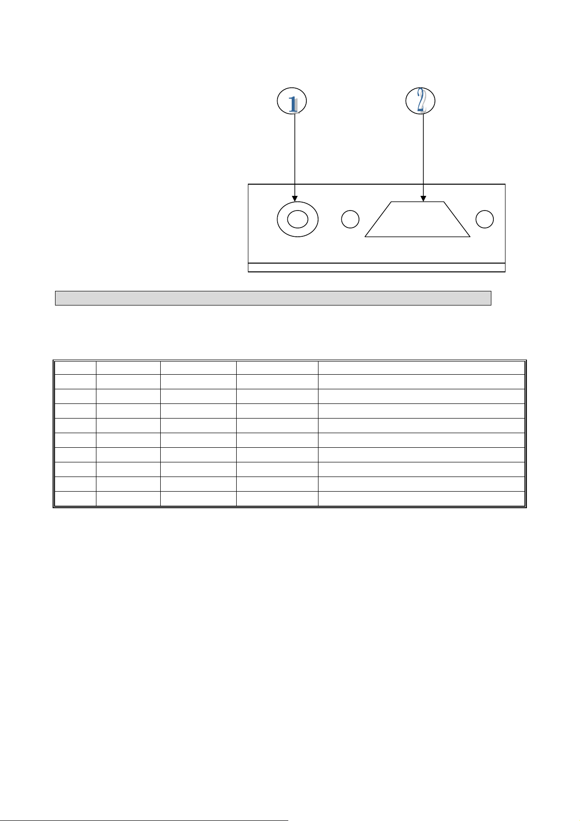
EXTERNAL CONNECTIONS
PIN
FUNCTION
TYPE
RANGE
DESCRIPTION
1-
50Ω BNC SOCKET
2-
9 WAY 〝 D 〞TYPE PLUG(J501)
2. CONNECTIONS AND OPERATION
D-TYPE INTERCONNECTIONS
J501-1 DATA_IN ANALOGUE 106mV EXTERNAL MODULATION INPUT
J501-2 DATA_OUT ANALOGUE 250~350mV RECEIVER AF OUTPUT
J501-3 PTT INPUT 0V/+5V TRANSMIT ENABLE
J501-4 GND GND 0V GND
J501-5 B+ V+ +13.8V POWER SUPPLY
J501-6 CDS OUTPUT OPEN/SHORT RF CARRIER DETECT
J501-7 NC
J501-8
J501-9 PGM_ENB INPUT 0V/5V PROGRAMMING ENABLE
PGM_DATA
INPUT 0V/NC PROGRAMMER DATA INPUT
PAGE3
Page 5

3. CIRCUIT DESCRIPTION
TRANSMITTER
The transmitter is comprised of:
• Audio amplifier connections from J1 pin 1
• Frequency Synthesizer
• Transmitter
• Automatic Power Control
Audio frequency connections
Processed data from the IC201 is applied to the VCO via R316
Frequency synthesizer circuit
With data received from the EEPROM (IC5) the frequency synthesizer circuit controls and
Produces the RF carrier frequency for the transmitter during transmit and the local oscillator
frequency for the receiver. The frequency synthesizer circuit is comprised of:
• 12.8 MHZ Tcxo
• Voltage Controlled Oscillator (VCO) module
• Charge Pump and Loop Filter
• PLL Frequency Synthesizer
• Dual Modulus Prescaler
PAGE4
Page 6
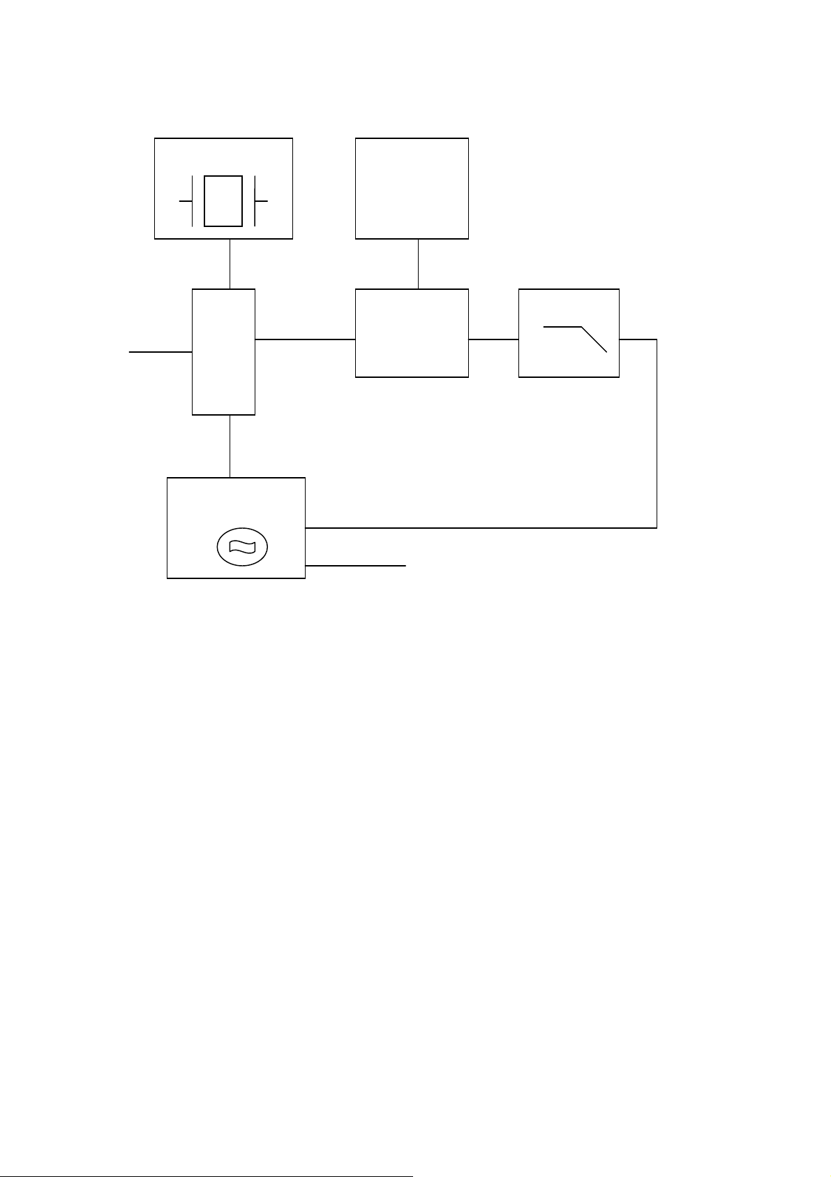
PLL Synthesizer
ains one VCO and three outputs. One for producing carrier frequencies during
The PLL synthesizer circuit is common to both the transmitter and receiver,
The synthesizer comprises:
Data
TCXO
IC1
PLL
DC
Regulator
Loop Filter
Charge Pump
TX OR RX
VCO
RF Out
12.8 MHZ TCXO
X1 is VCTCXO, which provide stable oscillator of 12.8 MHZ to PLL IC.
Frequency adjustment is provided by VR1.
.Voltage controlled oscillator module(VCO)
The module produces carrier frequencies during transmit and local oscillator frequencies
During receive.
The module cont
Transmit and one for producing the local oscillator frequency during receive and the other
Output is for PLL IC(IC1) Fin.
PAGE5
Page 7

The module also has Rx and TX powerline filters.
RX and TX power line filters
Transistor Q301 is configured as a 5v power supply ripple filter. The filter reduces the
noise on the carrier and local oscillator signals.
VCO
The VCO comprises Q302, Coil L304, and varactor D301 D304 and is configured
as a Colpits oscillator. D301 D304 produces a change in frequency with a change in DC voltage
and is controlled by the tuning voltage signal present at the cathode. The local oscillator
programmable dividers. DATA is received by IC1 at pin 10 from pin 11of IC3.
The RF signal at the collector of Q302 is applied to an amplifier/buffer Q305.The amplified
Signal from Q304 passes to the prescaler ,IC1 pin8 .The RF signal at the collector of Q302 also
Drives the cascode amplifier/buffer formed by Q304 .
When D201 is forward biased (TX ON) , carrier frequencies at the collector of Q304 pass to the
Power amplifier and harmonic filter. When D303 is forward biased (RX) , local oscillator
Frequencies at the collector of Q304 pass to the first mixer . VC1 adjusts the tuning
Voltage of the VCO to the correct operating point.
PLL IC
The reference frequency from the TCXO, at 12.8 MHZ , is connected to pin 1 of IC1(MB15E03)
REFDIV divides the 12.8 MHz to produce a reference frequency (Fr) of 5 or 6. 25 kHz
dependent upon channel spacing selected. VARDIV divides the prescaled VCO frequency
to produce a variable frequency (Fv). Fv and Fr are fed to the phase detector.
Phase detector
When Fv=Fr, the charge pump output produces a voltage fed into the loop filter and applied to the
VCO.
Out-of-lock detector
The out-of-lock detector produces a series of logic level pulses when the loop is out of lock at
pin 14 of IC1.The pulses at pin 14 of IC1 are buffered by Q6 and then integrated by R17 and
C19. The product of the integrating circuit is fed to Base of Q201.
PAGE6
Page 8
Charge Pump and Loop Filter
The IC1 pin5 and associated resistors make VCO loopFilter . The charge pump output
Produce a 0 to 5V tuning voltage signal.
The signal is filtered by the loop filter (R14,C15 and C20) to remove any residual reference
Frequency harmonics from the signal.. After filtering the signal is applied to the voltage controlled
Oscillator module.
DC REGULATOR
The DC Regulator IC2, converts the +13.6 V to a 8V supply . This is used to provide the
Tuning voltage for the VCO . A wide voltage range is required to allow for the wideband operation
Of the radio .
Dual modulus prescaler
The prescaler divides the VCO frequency by 64 or 65.
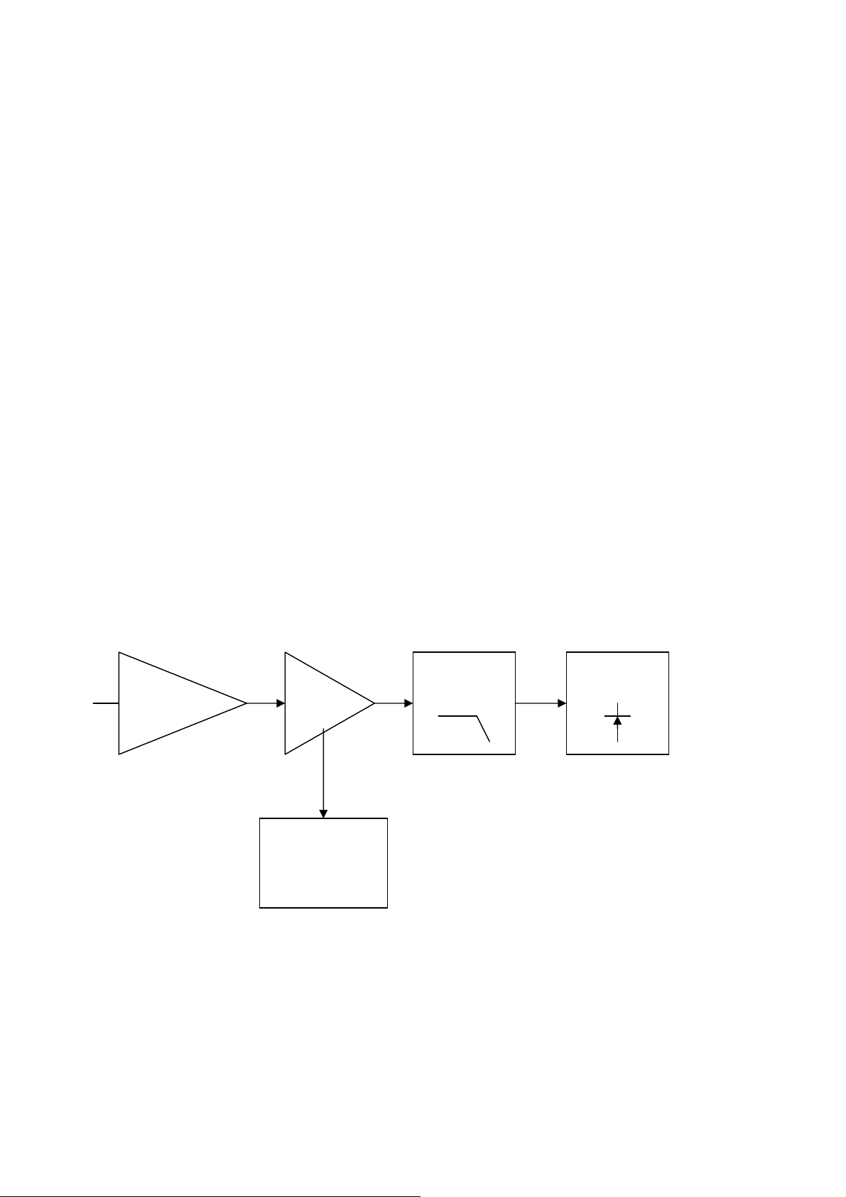
Transmitter
The transmitter comprises:
VCO Buffer PA Module
Amp
Automatic
Power Control
RF LPF
ANTENNA
SWITCH
PAGE7
Page 9

Buffer
When the radio is in transmit mode the diode D201 is forward biases enabling the
modulated RF signal from the VCO to pass to the buffer/pre-amplifier Q204 and
associated components.
The output signal is passed from Q204 to Q205 via a matching network consisting of
Inductor L201 and C208.
PA module
The signal is then amplified for transmission by Q207, which is a power amplifier module.
Low pass filter
The amplified RF signal is passed through the stripline coupler and is fed to the
harmonic low pass filter, comprising L213 to L214 and C232-C234 and then to the antenna
connector (ANT).
Antenna Switch
When transmitting, the diodes D205 are forward biased, the RF pass to the antenna.
D205 is shorted to ground which makes L212 look open circuit (1/4 wave
tuned stub). This prevents the TX signal from passing to the receiver stage.
PAGE8
Page 10
Receiver
The receiver comprises:
Rx
VCO
SAW FILTER&
ANTENNA
SWITCH
IFAmp
Amp
First Mixer
Second
Mixer
Local
Oscillator
IF Filter
IF
Filter
Data Out
Audio Filter
FM
Limiter-
Discnminator
Squelch
Circuit
PAGE9
Page 11

Antenna Switch
In receive, the diode D205 are reverse biased. L212 is now in circuit, passing
the signal from the antenna to the SAW filter of F101.
SAW FILTER
The receiver signal is routed to pin 4 of the F101. It passes through the
band pass filter .
The input signal is coupled to the base of Q101 which serves as an RF amplifier.
The output of Q101 is then coupled to the first mixer.
First Mixer
Q102, 2-pole crystal filters XF1 and coils L103 and C120 form the First Mixer
and First IF Filter.
The RF signal, from the SAW filter and amplifier Q101 is
applied to the VCO local oscillator signal to make mixer.
The difference frequency of 21.4 MHz is taken from Q102 and is filtered by the crystal
filters XF1. The tuned circuits L103 and C120 and associated components provide
matching of the crystal filters to ensure a good pass-band response and selectivity.
The IF signal is amplified by Q104 and passed to the FM Detector IC.
Second mixer, Second IF, FM detector
The output of the IF amplifier is fed into the narrowband FM IF Integrated Circuit,
IC101 (MC3361). This is a single conversion FM receiver which contains the second
mixer, second IF amplifier, and FM detector.
PAGE10
Page 12

Crystal X101,connected to pin 1 of IC101, determines the second local oscillator frequency.
In this case the crystal has a frequency of 20.945MHz. The first IF signal is applied to
the mixer and resultant frequency of 455KHz, is the difference between the IF signal
and second local oscillator.
The 455KHz IF signal is output from pin 3 and is applied to a 455KHz band-pass filter CF1.
The output of CF1is passed via pin 5 to a high gain IF amplifier coupled to the
adjustable quadrature detector T2.Any detected signal is produced at pin 9 of
IC101 and applied to the Receiver Audio Circuit and the Mute (Squelch) Circuit.
Squelch ( MUTE ) Circuit
Any noise signal is amplified by IC101 internal noise
Signal is applied to pin10 of IC101. The squelch trigger output (pin 12,IC101) is applied to the
pin 6 of J1.
When noise is present, the voltage at pin 12 of IC101 is exceeds than 0.7V. The squelch trigger
output is open, It’s make pin 6 of J1 open state.
When no noise is
Is HI voltage. This make pin 6 of J1 short state.
VR101 is set to tuning squelch when 25khz channel space is present.
Carrier Detect
A Carrier Detect ( MUTE DETECT ) output is available on pin 6 of J1 .
AF Output Low Pass Filter
A low pass filter formed by R108 and C110 removes any extraneous 455kHz energy
from the AF output of the FM receiver chip (pin 9 of IC101).
present, the
voltage at pin 12 of IC101 less 0.7v and pin 13 of IC101
amplifier .
The filtered signal is passed to pin 2 of J1.
Microcontroller
The PIC16C57C04 microcontroller IC controls the programmable features and frequency synthesizer
Data.
PAGE11
Page 13

Programming Mode
The programming mode allows the user to retrieve or program TX/RX frequencies,
when pin 9 of J1 is set to ground. Programming mode will Inhibit ,
Serial communications can then be made in order to read/program the on- board
EEPROM ( IC5 )which contains radio- specific data.
EEPROM
Relevant channel information, such as Rx/ Tx frequencies, is stored in the EEPROM( IC5)
which is a 93C46. This information may be programmed and erased via the D- type socket.
The EEPROM has 1024 (8x128) capacity and is written serially.
Power supply circuit
The data radio is supplied with a nominal + 13.8V dc power supply input from external
equipment which is filtered using C33. This supply is converted into 8V
voltage levels on the board using the regulator IC2 and associated components .
The +5V VCC is regulated by Zener diode D1 and filtered using C9 and Q9. This +5V
line is fed to the CPU circuit .
4. PERFORMANCE TEST AND ALIGNMENT
The alignment and performance test procedures assume the use of the following equipment.
Discrete test equipment
Volt Meter Spectrum Analyser and notch filter(option)
RF Power Meter. Coupler (20dB isolation)
DC Power Supply, 0-15V 2Amin Distortion Meter
Oscilloscope, 20 MHz dual beam
RF Frequency Counter,
100 kHz - 600 MHz
AF Signal Generator 0 – 20 kHz
RF Signal Generator
SINAD Meter
Modulation Meter
Audio Power Meter
PAGE12
Page 14

5
. TEST EQUIPMENT CONFIGURATION.
RF Signal Generator
Watt Meter with
20dB Attenuator
Audio Generator
Modulation Meter
SINAD Meter OSCILLOSCOPE
RADIO
VOLT Meter
DC Power Supply
Spectrum Analyzer
Frequency Counter
123.45678
Test Box
Test Equipment Configuration
PAGE13
Page 15

6. TRANSMITTER PERFORMANCE TESTS
Power Output
1. Set the power supply voltage to 13.8V dc. and monitor the voltage during transmit.
2. Switch data radio TX and check and record the output power. The nominal output
power is adjustable between 2 to 3W .
3. Set the PTT switch to OFF .
Peak Deviation
1. Connect the oscilloscope to the output of the modulation meter.
2. Set the AF signal generator to 1000 Hz at 106mV and connect to DATA _IN
Line ( pin 1 of J1 )
3. Switch data radio to TX and observe the oscilloscope display to check that the 1000Hz
tone is a sine wave and adjust VR201 to make deviation is about 3.5KHZ.
4. Using the AF signal generator, sweep from 100 Hz to 3 kHz and record the peak
deviation.
5. Check the peak deviation for appropriate channel spacing as follows:
For 12.5 kHz channel spacing, Peak deviation is not greater than 2.5 kHz.
For 20 kHz channel spacing, Peak deviation is not greater than 4 kHz.
For 25 kHz channel spacing, Peak deviation is not greater than 5 kHz.
Spectrum Test
It may be necessary to notch the fundamental signal during this test.
1. Connect a spectrum analyser and RF power meter to the antenna socket.
2. Switch data radio to TX. Observe the output spectrum on the spectrum analyser.
3. Adjust notch filter to minimise the carrier. All spurious and harmonics signals
should be below- 36 dBm up to 1 GHz and below –30 dBm between 1 and 4 GHz.
4. Switch off the data radio transmit control.
Receiver Performance Tests
Sensitivity
The SINAD performance test may be used to test the sensitivity of the receiver.
1. Connect the RF signal generator to the data radio BNC antenna connector.
2. Set the RF signal generator to the receive frequency .
3. Connect the leads of the SINAD meter between 0 V and pin 2 on J1.
4. Set the deviation to 60﹪of the peak system deviation.
5. Set the AF generator to 1 kHz.
6. Adjust the RF signal generator level until the SINAD Meter reads 12 dB.
7. Check that the signal generator RF level is less than 0.35uV pd (-116dBm ).
PAGE14
Page 16

TransmitterAlignment
Automatic PowerAdjustment
Transmit periods longer than 3 minutes are to be avoided.
1. Switch to data radio to TX.
2. make the transmit power between 2 to 3W.
3. Switch the data radio to transmitter OFF.
Frequency accuracy
1. Whilst transmitting, measure the transmit frequency using the RF frequency counter.
2. Adjust VR1 so that frequency is as close as possible to the exact required transmit
frequency. Ideally it should be within 100 Hz at room temperature.
ReceiverAlignment
Important note:Before setting up the receiver it is important to check the frequency
accuracy alignment is correct as described in the transmitter alignment section.
RF tuning
1. Connect an RF signal generator and SINAD voltmeter.
2. Set the RF signal generator to the receive channel frequency and set to 60﹪deviation.
3. Set the AF signal to 1 kHz.
4. Set the RF level to 1 mV pd (- 47.0 dBm )
5. Adjust T2 for maximum AF output about 250mVto 350mV and lowest distortion,
the distortion normally less than 5﹪.
6. Check for an RF voltage signal level of 0.35uV pd (- 116dBm)and a SINAD meter
Reading greater than 12 dB.
Squelch/Carrier Detect Adjustment
1. Set the RF signal generator to the receiver frequency with 60﹪deviation. Set the AF
Signal to 1 kHz
2. Set RF input level to give -112 dBm.
3. Adjust VR101 until CDS J1 pin 6 changes state from “HIGH”to “LOW”.
4. Reduce RF input level to –120dBm and check that CDS line goes HIGH . Switch
off the RF generator and disconnect the test equipment.
PAGE15
Page 17

Modulation DeviationAdjustment
1. Connect a power meter, modulation meter and oscilloscope to radio.
2. The radio should be programmed to contain a channel with a frequency in the middle
the band of interest with an RF power setting of 2 W.
3. Switch the data radio ON.
4. Inject a 106mVrms SINE wave signal at a frequency of 1000Hz into pin 1 of J1,
Set the data radio to TX Observe the oscilloscope display to check that the 1000Hz tone
is a sine wave by tuning VR201and set deviation is 3.5KHZ.
5. Using the AF signal generator, sweep from 100 Hz to 3 kHz and record the peak
deviation.
Check the peak deviation for appropriate channel spacing as follows:
12.5 kHz channel spacing<= 2.5 kHz dev
20 kHz channel spacing<= 4 kHz dev
25 kHz channel spacing<= 5 kHz dev
6. Switch to RX.
PAGE16
Page 18

7. TROUBLESHOOTING
Ref. No.
BCE
The section includes voltage which should assist the engineer to isolate and repair the fault.
Voltage measurements should be made using a high-impedance voltmeter and the values given
are with respect to ground.
Careful alignment, using suitable test equipment, and quality interface cables should
ensure that the radio meet their specified performance.
Voltage Charts
Measurement Condition: 465MHZ,13.8V supply, RX Carrier Present.
Transistors .
RX TX
B C E
Q1 4.31 4.98 4.99 4.31 4.98 4.99
Q6 4.91 0 4.93 4.9 0 4.92
Q7 0 8.0 0 4.93 0.02 0
Q9 5.64 8.0 4.99 5.63 7.8 4.96
Q10 4.16 8.0 3.76 4.15 7.8 3.75
Q11 6.17 8.0 5.46 6.17 8.0 5.46
Q14 8.0 0.2 8.0 7.08 7.63 7.8
Q15 7.56 8.0 6.84 0.62 7.8 0
Q101 0.74 3.93 0 0 0 0
Q102 0.68 6.67 0 0 0 0
Q103 5.11 0 0 0 0 0
Q104 0.68 4.71 0 0 0 0
Q201 0 0 0 0 0.72 0
Q202 0 0 0 0.73 0 0
Q203 0 0 0.3 0 7.36 7.92
Q204 0 0 0 0.75 7.35 0
Q205 0 0 0 0.7 7.36 0.25
Q206 0 12.36 0 0.56 5.92 0
Q207 0 13.6 0 0 13.6 0
Q301 4.87 4.92 4.2 4.87 4.92 4.2
Q302 1.63 3.99 0.92 1.63 3.99 0.92
Q304 0.74 2.77 0 0.74 2.77 0
PAGE17
Page 19

Integrated Circuits
Pin
IC2
IC3
IC4
IC5
RECEIVER
IC1
1 1.25 13.6 0 5 0 5.51 0
2 1.22 8.0 5 5 0 4.93 0
3 5.47 0 0 0 5 5.24 0
4 2.99 0 5 0 5.59 0
5 1.24 0 5 0 4.38 0
6 0 5 4.08 4.37 0
7 2.21 4.96 0 4.38 0
8 2.1 0 5 5.08 0
9 0 0 2.23
10 0 0 0.74
11 0 0 3.71
12 2.99 0 0.93
13 2.99 0 5.21
14 2.99 0 0
15 0 0 0
16 0 0 1.75
17 5
18 0
19 5
20 5
21 0
22 0
23 5
24 5
25 5
26 0.66
27 1.03
28 5
IC101 IC201
Integrated Circuit Voltages (Receive)
PAGE18
Page 20

Integrated Circuits
TRANSMIT
PIN
1 1.25 13.6 0 0.58 0 0 1.16
2 1.22 8.0 5 0.58 0 0 0
3 5.47 0 0 0 5 0 0
4 2.99 0 0.34 0 0 0
5 3.59 0 5 0 0 2.43
6 0 0.34 4.08 0 5.03
7 2.21 4.92 0 0 2.48
8 2.1 0 5 0 1.17
9 0 0 0
10 0 0 0
11 0 0 0
12 2.99 0 0
13 2.99 0 0
14 2.99 0 0
15 0 0 0
IC1 IC2 IC3 IC4 IC5 IC101 IC201
16 0 0 0
17 4.98
18 4.95
19 4.98
20 0
21 0
22 0
23 4.98
24 4.98
25 4.98
26 0.66
27 1.03
28 5
Integrated Circuit Voltages (Transmit)
PAGE19
Page 21

8. PARTS LIST
52-7085UE5 Revised: June 4, 2015
Revision:
Bill Of Materials June 4, 2015 13:59:51
Item Quantity Reference Part
_____________________________________________________________
1 22 C1,C3,C40,C47,C48,C49, 470P
C51,C52,C106,C201,C216,
C217,C218,C221,C225,C227,
C235,C237,C238,C239,C244,
C250
2 11 C2,C108,C249,C317,C550, 1U/Y5V 0805
C552,C553,C554,C555,C556,
C558
3 5 C4,C127,C224,C234,C236 5P
4 17 C5,C7,C8,C10,C14,C44, 102P
C103,C107,C121,C126,C202,
C203,C207,C245,C307,C312,
C322
5 1 C9 475P/0805
6 15 C13,C19,C36,C37,C41,C42, 104P
C46,C53,C67,C102,C111,
C112,C117,C251,C546
7 1 C15 0.47U/T
8 3 C16,C17,C21 103P/X7R
9 5 C18,C35,C118,C205,C241 10U/1206
PAGE20
Page 22

52-7085UE5 Revised: June 4, 2015
Revision:
Bill Of Materials June 4, 2015 13:59:51
Item Quantity Reference Part
_____________________________________________________________
10 1 C20 333P/X7R 0805
11 6 C30,C31,C32,C45,C116, 47P
C523
12 1 C33 47U/16V/EC/SMT
13 1 C34 100U/16V/EC/SMT
14 4 C43,C50,C120,C223 22P
15 1 C101 1P
16 2 C104,C252 1U/T
17 1 C105 104P/X7R 0603
18 2 C110,C247 223P/X7R 0603
19 1 C113 180P
20 4 C115,C122,C308,C524 100P
21 2 C123,C214 15P
22 4 C125,C212,C220,C311 2P
23 2 C204,C302 18P
24 1 C206 6P
25 4 C208,C213,C230,C314 3P
PAGE21
Page 23

52-7085UE5 Revised: June 4, 2015
Revision:
Bill Of Materials June 4, 2015 13:59:51
Item Quantity Reference Part
_____________________________________________________________
26 4 C210,C232,C233,C323 10P
27 3 C211,C305,C306 7P
28 1 C222 12P
29 5 C240,C300,C301,C309,C325 220P
30 1 C242 10U/T
31 1 C243 104P/X7R/0805
32 4 L217,C246,C253,C254 NU
33 1 C303 9P
34 1 C304 8P
35 1 CF1 CFU455E
36 2 D1,D103 RLZ5.6B
37 4 D2,D3,D101,D202 RLS4148
38 1 D4 RLZ4.3B
39 1 D5 RLZ6.2B
40 2 D6,D507 RLZ3.0B
41 1 D102 1SS226
42 1 D201 1SS314
PAGE22
Page 24

52-7085UE5 Revised: June 4, 2015
Revision:
Bill Of Materials June 4, 2015 13:59:51
Item Quantity Reference Part
_____________________________________________________________
43 1 D203 PTZ5.6B
44 3 D205,D206,D303 HVU131
45 1 D209 FM4004
46 2 D301,D304 1SV229
47 1 F101 SAW FILTER
48 1 IC1 MB15E03SL
49 1 IC2 UTC7808
50 1 IC3 PIC16F57 SMT
51 1 IC4 ELM7S32
52 1 IC5 93C46 SMT
53 1 IC6 RT9161-50PV
54 1 IC101 MC3361 SMT
55 1 IC201 LM386D
56 1 IC504 TL064CD SMT
57 1 J1 CONNECTOR DB9 HM
58 1 J101 BNC
59 1 L101 12NH
PAGE23
Page 25

52-7085UE5 Revised: June 4, 2015
Revision:
Bill Of Materials June 4, 2015 13:59:51
Item Quantity Reference Part
_____________________________________________________________
60 1 L102 39NH/0805
61 1 L103 2.2UH/BEAD
62 2 L201,L303 27NH
63 1 L202 15NH
64 1 L203 18NH
65 1 L204 0.45*1.5*6T
66 2 L205,L206 5.6NH/0603
67 1 L208 0.4*3*9T
68 1 L210 0.65*1.1*4T
69 1 L212 0.45*1.5*5T
70 2 L213,L214 0.65*1.45*4T
71 1 L215 2.2UH/1008
72 1 L216 125MH
73 2 L218,R517 0R
74 2 L300,L301 1UH/0805
75 1 L304 12NH/0805
76 2 Q1,Q6 2SA1037K
PAGE24
Page 26

52-7085UE5 Revised: June 4, 2015
Revision:
Bill Of Materials June 4, 2015 13:59:51
Item Quantity Reference Part
_____________________________________________________________
77 2 Q7,Q103 DTC114EK
78 6 Q9,Q11,Q15,Q201,Q202, BC847B
Q301
79 1 Q14 BCW68G
80 1 Q101 2SC5084
81 5 Q102,Q204,Q205,Q302,Q304 HSC5262
82 1 Q104 HSC1010
83 1 Q203 DTA123JK
84 1 Q206 BFG35
85 1 Q207 2SK3476
86 10 R1,R17,R50,R201,R203, 10K
R205,R308,R518,R521,R524
87 8 R3,R47,R118,R516,R523, 100K
R525,R528,R531
88 3 R9,R22,R224 820R
89 10 R10,R20,R29,R40,R46,R51, 1K
R52,R202,R223,R317
90 1 R13 3.01K
91 2 R14,R15 9.09K
PAGE25
Page 27

52-7085UE5 Revised: June 4, 2015
Revision:
Bill Of Materials June 4, 2015 13:59:51
Item Quantity Reference Part
_____________________________________________________________
92 2 R16,R111 33K
93 2 R23,R304 150R
94 6 R24,R41,R45,R107,R219, 4.7K
R307
95 5 R48,R49,R117,R204,R216 470R
96 2 R53,R102 1M
97 9 R60,R61,R248,R526,R527, 47K
R532,R533,R534,R546
98 5 R101,R222,R309,R315,R316 100R
99 3 R103,R221,R318 2.2K
100 1 R104 220K
101 3 R105,R208,R220 22K
102 1 R106 1.5M
103 3 R108,R212,R311 2.7K
104 3 R110,R112,R113 560R
105 1 R114 1.2K
106 2 R115,R217 470K
107 3 R116,R211,R213 22R
PAGE26
Page 28

52-7085UE5 Revised: June 4, 2015
Revision:
Bill Of Materials June 4, 2015 13:59:51
Item Quantity Reference Part
_____________________________________________________________
108 1 R206 1.5K
109 1 R207 220R
110 1 R210 3.3K
111 1 R214 22R/1206
112 1 R218 27K
113 2 R226,R313 56R
114 1 R301 10R
115 1 R302 5.6K
116 1 R303 3.9K
117 1 R306 33R
118 1 R545 680R
119 1 RP1 10K*4
120 2 RV501,RV502 10KB SMT
121 1 SW1 CH SW
122 1 T2 1766
123 1 VC1 20PVC
124 1 VC2 10PVC/DIP
PAGE27
Page 29

52-7085UE5 Revised: June 4, 2015
Revision:
Bill Of Materials June 4, 2015 13:59:51
Item Quantity Reference Part
_____________________________________________________________
125 1 VC3 5PVC/SMT
126 1 VC4 10PVC/SMT
127 1 VR1 100KB SMT
128 1 VR101 47KB/SMT
129 1 X1 12.8MHZ TCXO/SMT
130 1 X2 3.58MHZ 3X9
131 1 X101 20.945MHZ UM1
132 1 XF1 21M08B
PAGE28
Page 30

Welcome to PC Programmer.
Please Read this file, before you first use the software.
TABLE OF CONTENTS
1. Brief introduction
2. Before Installing
3. Install PC Programmer
4. INSTRUCTIONS
5. UnInstall PC Programmer
1. Brief introduction
Welcome to PC Programmer. This program is designed to be used with the
Interface Adapter.
The following equipment will be needed to program the Device:
A. A computer to install this program with at least 2 MB available space
in hard disk and a 9-pin male RS-232 serial port.
B. Win 95,Win 98,Win ME or Win 2000 Operation System.
C. Part of the Programming Kit
1) An interface Adapter.
2) A CD disk with the program, PC Programmer files
2. Before Installing
Before You Run Setup, make sure that your computer meets the minimum
requirements mentioned above, and read the Readme file(this file).
NOTE: If you firstly install PC Programmer in you system, the setup may
update some system files on your computer , so you may run the
setup again after your system be updated. Please follow the
installation instruction on the screen.
3. Install
TO install PC Programmer on your computer
1)Insert the CD.
2)Run Setup.exe
3)Follow the installation instruction on the screen.
Important: You cannot simply copy files from the CD to your hard disk
and run PC Programmer . You must use the Setup program,
which decompresses and installs the files in the appropriate
directories. PAGE 29
Page 31

4. INSTRUCTIONS
4.1 Connection
4.2 Start up PC Programmer
4.3 Edit Configuration
4.3.1 Open/Recall/Upload Configuration file
4.3.2 Edit Channel data
4.3.3 Set Option item
4.3.4 (Block)Cut/Copy/Delete/Paste
4.3.5 Auto-Frequency edit
4.3.6 Save a Configuration to disk
4.3.7 Download Configuration to device
4.3.8 Print a Configuration
4.4 Exit PC Programmer
4.1 Connection
1.Connect one side of Interface Adapter to the computer's serial port.
Never care the port number, the PC Programmer will locate it
automatically.
2.Connect the other side of Interface Adapter to the Device's 9-pin
male RS-232 port.
3.Connect power supply to device and LED will be light. The device will into
PC_programming mode automatically, please see the picture of below.
PAGE30
Page 32

4.2 Start up PC Programmer
1.Select 'Start', choose 'Programs', click on the '*** Serial PC
Programmer' program.
2.When HD Serial PC Programmer is started, a main form will be shown
after a greeting form.
3.There has a menu bar at the top of the main form, and a message box
at the bottom.
PAGE31
Page 33

NOTE:The program is menu driven for all pertinent commands. All the
commands can be accessed by either key board or the left mouse
button.
Access keys mainly used are:
'Tab' or 'Arrow' to move focus(or cursor)
'Enter' to active a focused command
4.3 Edit Configuration
4.3.1 Open/Upload Configuration file
To edit the configuration, please either
1)Recall an Existing Configuration by click on the 'Open' item in
the File Menu, select the configuration file by click on or input
its name then press 'Enter' key.
OR 2)Upload configuration data from a device by click on 'Upload' item
in the Device menu. to a Configuration window .
Different Model's device Configuration can be opened and edited.
There are two fields in each Configuration window: system data
and Channel data.
OR 3)Open an existing Configuration by click on the 'OPEN' item in the
File Menu. A pop up window will be shown, select a file by arrow
key or mouse then click 'OK'.
4.3.2 Edit Channel data
1)Set focus to the Channel data field by move the mouse pointer.
2)Select a particular channel number to be edited by either the
arrow key or click on it.
3)Pop up input window by either press 'Enter' key or double click
on the selected channel number.
4)Use computer's cursor keys, Tab key, Enter key, arrow key or
mouse to renew the channel data.
5)Click 'OK' button on the input window to accept the change or
'Cancel' to not change, and return back to Configuration Window.
4.3.3 Edit Option item
1)To Edit Channel Option, Select a particular channel number in
the Option View Window by either the arrow key or click on it,
then Pop up the input window for Channel Option, 'Enter' key or
double click on the selected channel number.
PAGE32
Page 34

2)To Edit System Option, Pop up input window for System Option,
click "SYSTEM" in the 'OPTION' menu.
3)To Edit Advanced Option, Pop up input window for Advanced Option,
click "ADVANCED OPTION" in the 'OPTION' menu.
4Use computer's cursor keys, Tab key, Enter key, arrow key or
mouse to renew the Option Item.
5)Click 'OK' button on the input window to accept the change or
'CANCEL' to not change, and return back to Configuration Window.
4.3.4 (Block)Cut/Copy/Delete/Paste
To select a block of channel data as source by either
1)Select start channel by arrow key, then while press 'Shift' key
select end channel number by arrow key.
2)Click on start channel, then while press 'Shift' key click on
end channel number
3)Press the left mouse button on start channel then move the mouse
until reach the end channel number, release left mouse button.
A)To Cut selected (block) Channel(s) either press 'Ctrl'+'X'or
click 'CUT' item in Edit menu.
B)To Copy selected (block) Channel(s) either press 'Ctrl'+'C'or
click 'COPY' item in Edit menu.
C)To Delete selected (block) Channel(s) either press 'Del(Delete)'
key or click on 'DELETE' item in Edit menu.
After Cut or Copy, the data can be pasted to where you want.
D)To Paste , select a channel as the start number of target , then
either press 'Ctrl'+'V' or click on 'PASTE' item in Edit menu.
NOTE: Paste operation allows you to export data to any Configuration
window opened.
4.3.5 Auto-Frequency edit
This feature provide you with a quick Frequency set function.
To use this command after either
1)Click 'EDIT' Menu
2)Click on 'AUTOFREQ' item in 'EDIT' menu to pop up a input window.
3)Use computer's cursor keys, Tab key, Enter key, arrow key or mouse
to set data.
4)Click 'OK' button on the input window to accept the change or
'CANCEL' to not change, and return back to Configuration Window.
PAGE33
Page 35

4.3.6 Save a Configuration to disk
1)Different configuration can be saved to disk.
2)Click on 'SAVE' item in 'FILE' Menu will overwrite an existing
configuration file on your disk by current configuration.
3)Select 'SAVE AS' from 'FILE' Menu will save the current
configuration by a name as you prefer.
4.3.7 Download to device
To Download current Configuration to device, select 'DOWNLOAD' from
sub menu under 'DEVICE' menu.
4.3.8 Print a Configuration
Click on 'PRINT' item in 'FILE' Menu will send current Configuration
to printer.
4.4 Exit PC Programmer
To Exit PC Programmer,click on 'EXIT' item in 'FILE' Menu.
5. UnInstall PC Programmer
To uninstall PC Programmer from your hard disk, select 'Start'
, choose 'Settings', click on the 'Control Panel', then find 'Add/Remove
Programs' icon from the pop up window then double click on it, then find
'*** Serial PC Programmer' from application list and click on it, then click
on 'Add/Remove' button under application list, then follow the
instructions on your screen.
PAGE34
Page 36

TOP LAYER PCB LAYOUT
BOTTOM LAYER PCB LAYOUT
PAGE35
Page 37

CAM350 V 5.0 : Thu Jun 4 15:08:51 2015 - (Untitled)
Page 38

CAM350 V 5.0 : Thu Jun 4 15:09:15 2015 - (Untitled)
Page 39

8
12.8MHZ
TCXO SMT
X1
D D
TCXO MOD.
PLL CONTROL
OSC
3V
REG
IC1
7
R
V
FIN
LD
Q2,Q4
2 1
21
Q201
3
Q6
6
LOOP FILTER
VCO
CONT
TXB+5V
Q202
2
3
3
2
1
1
Q203
1SV229
VCO
D301
5
VCO
RF OUT
1
D304
1SV229
2SC3356
Q305
Q304
2SC3356
2
3
2
3
1
D303
4
TX SW
D201
CASCODE
DRIVER
Q204,Q205,Q206
3
PA TRANSISTOR
Q207
+13.6V
TX/RX SW
2
L212
D205
L.P.F
ANT
BNC
1
8V
VP
1
6
2
7
3
8
4
9
5
POWER SUPPLY
UNIT
CDS AF OUT
5V
PGM ENABLE
PGM DATA
PTT
IC4
RESET
Q1
TX+5V
IC201
PLL
DATA
BUS
IC3
PIC16C57C04
TXEN1
VR201
Q7
21
+13.8V
C C
J1
B B
MOD INPUT
TXEN1
XF1
1ST IF FILTER
RX SW
Q15
TXEN1
2 1
Q102
1ST
MIXER
Q104
1ST IF AMP
TXEN1
RX +5V
TX SW
Q14
20.945MHZ
MIXI
X101
OSC MIX
RX+5V
Q101
RF AMP
CF1
IC101
2ND IF I/P
SAW FILTER
QUADRATURE
DETECTOR COIL
T2
CDS
SCAN CONT
SQ INAF OUT FIL IN FIL OUT
Q7
D102
CS DAT CLK
AF OUT
A A
EEPROM
IC5
8
7
6
5
4
NOISE FILTER
3
VR101
SQUECLH
2
HERMES ELECTRONICS CO., LTD
Title
52-7085-UE2
Size Document Number Rev
Custom
Date: Sheet of
0 0Wednesday, August 20, 2008
1
Page 40

Federal Communication Commission Interference Statement
This equipment has been tested and found to comply with the limits for a Class B digital device,
pursuant to Part 90 of the FCC Rules. These limits are designed to provide reasonable
protection against harmful interference in a residential installation. This equipment generates,
uses and can radiate radio frequency energy and, if not installed and used in accordance with
the instructions, may cause harmful interference to radio communications. However, there is
no guarantee that interference will not occur in a particular installation. If this equipment does
cause harmful interference to radio or television reception, which can be determined by
turning the equipment off and on, the user is encouraged to try to correct the interference by
one of the following measures:
Reorient or relocate the receiving antenna.
Increase the separation between the equipment and receiver.
Connect the equipment into an outlet on a circuit different from that to which the
receiver is connected.
Consult the dealer or an experienced radio/TV technician for help.
FCC Caution: Any changes or modifications not expressly approved by the party responsible
for compliance could void the user's authority to operate this equipment.
This device complies with Part 90 of the FCC Rules. Operation is subject to the following two
conditions: (1) This device may not cause harmful interference, and (2) this device must
accept any interference received, including interference that may cause undesired operation.
Changes or modifications not expressly approved by the party responsible forcompliance
could void the user's authority to operate the equipment.
The antenna(s) used for this transmitter must not be co-located or operating inconjunction
with any other antenna or transmitter
Operation is subject to the following two conditions: (1) this device may not cause interference, and (2) this
device must accept any interference, including interference that may cause undesired operation of the device.
To reduce potential radio interference to other users, the antenna type and its gain should be so chosen that
the equivalent isotropically radiated power (EIRP) is not more than that required for successful communication
This device has been designed to operate with an antenna having a maximum gain of [4.8] dBi. Antenna having
a higher gain is strictly prohibited per regulations of Industry Canada. The required antenna impedance is 50
ohms.
To reduce potential radio interference to other users, the antenna type and its gain should be so chosen that
the equivalent isotropically radiated power (e.i.r.p.) is not more than that permitted for successful
communication.
FCC Radiation Exposure Statement
This equipment complies with FCC RF radiation exposure limits set forth for an
uncontrolled environment. This equipment should be installed and operated with a
minimum distance of 0.8 m between the radiator and your body.
This transmitter must not be co-located or operating in conjunction with any other
antenna or transmitter.
The antennas used for this transmitter must be installed to provide a separation
distance of at least 0.8 m from all persons and must not be co-located or operating in
conjunction with any other antenna or transmitter
 Loading...