

AEROFLEX ACT-S512K32V Service Manual
查询ACT-S512K32V供应商
ACT-S512K32V High Speed 3.3Volt
16 Megabit SRAM Multichip Module
Features
■ 4 Low Power CMOS 512K x 8 SRAMs in one MCM
■ Overall configuration as 512K x 32
■ Input and Output TTL Compatible
■ 17, 20, 25, 35 & 45ns Access Times, 15ns Available by
Special Order
■ Full Military (-55°C to +125°C) Temperature Range
■ +3.3V Power Supply
■ Choice of Surface Mount or PGA Type Co-fired Packages:
● 68–Lead, Dual-Cavity CQFP (F2), .88"SQ x .20"max (.18"max
thickness available, contact factory for details) (Drops into the
68 Lead JEDEC .99"SQ CQFJ footprint)
● 66–Pin, PGA-Type (P1), 1.38"SQ x .245"max
● 66–Pin, PGA-Type (P7), 1.08"SQ x .185"max
■ Internal Decoupling Capacitors
■ DESC SMD# Pending
CIRCUIT TECHNOLOGY
www.aeroflex.com/act1.htm
General Description
The ACT–S512K32V is a High
Speed 4 megabit CMOS SRAM
Multichip Module (MCM)
designed for full temperature
range, 3.3V Power Supply,
military, space, or high reliability
mass memory and fast cache
applications.
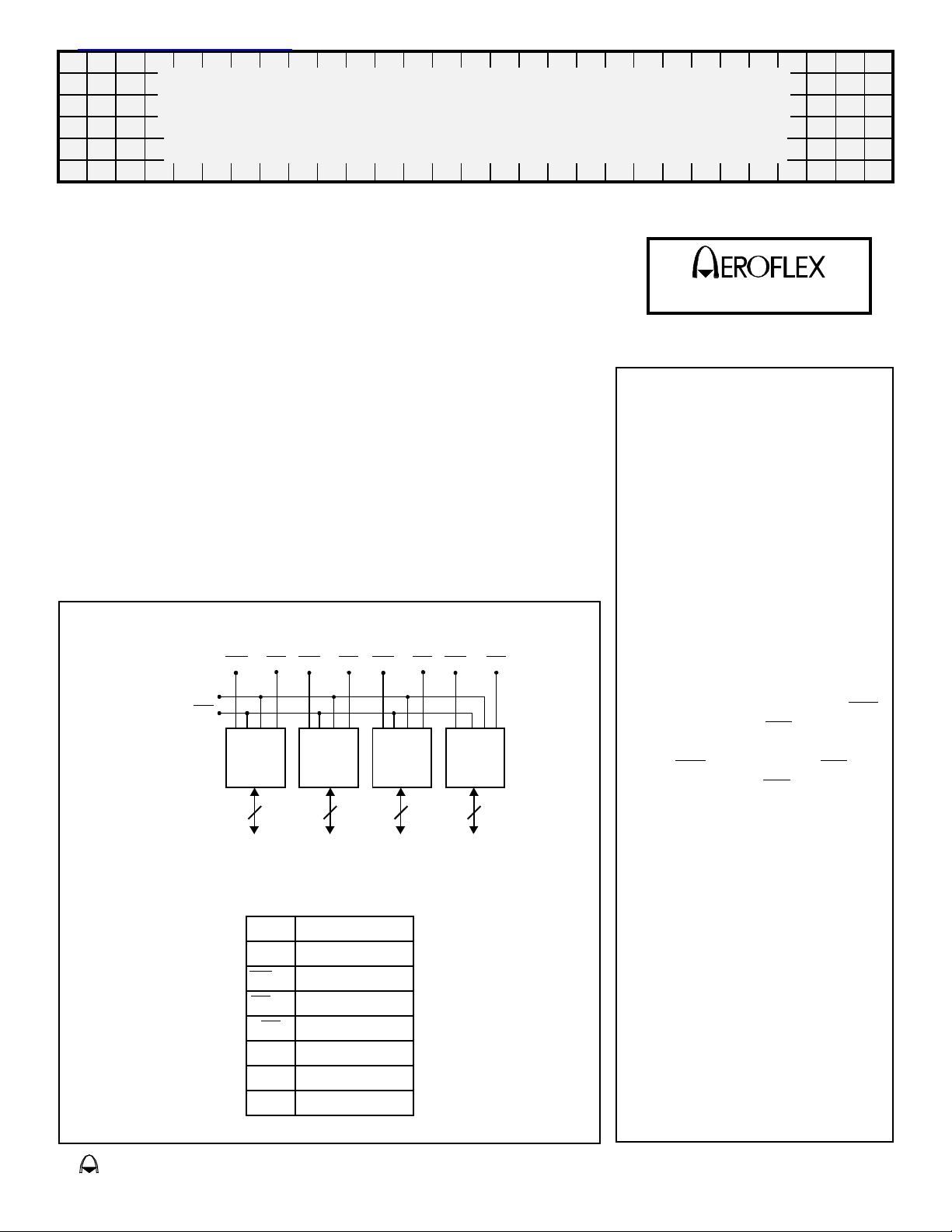
Block Diagram – PGA Type Package(P1,P7) & CQFP(F2)
CE4
A0 – A18
OE
CE3 WE4WE3WE2WE1 CE1 CE2
512Kx8 512Kx8 512Kx8 512Kx8
8 8 8 8
I/O0-7 I/O8-15 I/O16-23 I/O24-31
I/O
A
WE
CE
Pin Description
0-31 Data I/O
0–18 Address Inputs
1–4 Write Enables
1–4 Chip Enables
Output Enable
OE
cc Power Supply
V
GND Ground
NC Not Connected
The MCM can be organized
as a 512K x 32 bits, 1M x 16
bits or 2M x 8 bits device and is
input and output TTL
compatible. Writing is executed
when the write enable (WE
and chip enable (CE
) inputs are
low. Reading is accomplished
when WE
output enable (OE
is high and CE and
) are both
low. Access time grades of
17ns, 20ns, 25ns, 35ns and
45ns maximum are standard.
The products are designed for
operation over the temperature
range of -55°C to +125°C and
screened under the full military
environment. DESC Standard
Military Drawing (SMD) part
numbers are pending.
The ACT-S512K32V is
manufactured in Aeroflex’s
80,000ft
2
MIL-PRF-38534
certified facility in Plainview,
N.Y.
)
eroflex Circuit Technology - Advanced Multichip Modules © SCD3360 REV B 12/17/98
Absolute Maximum Ratings
Symbol Rating Range Units
Speed 15ns -40 to +85 °C
Speed 17ns to 45ns -55 to +125 °C
-65 to +150 °C
3.0 W
2.7 W
2.0 °C/W
8.0 °C/W
-0.5 to +4.6 V
300 °C
T
Ø
T
STG
P
J-C
V
T
C
Case Operating Temperature
Storage Temperature
D
Maximum Package Power Dissipation
P1,P7 Package
F2 Package
Hottest Die, Max Thermal Resistance - Junction to Case
P1,P7 Package
F2 Package
G
L
Maximum Signal Voltage to Ground
Maximum Lead Temperature (10 seconds)
Normal Operating Conditions
Symbol Parameter Minimum Maximum Units
V
CC
V
IH
V
IL
Power Supply Voltage
Input High Voltage
Input Low Voltage
+3.0 +3.6 V
+2.0 V
+ 0.3 V
CC
-0.3 +0.8 V
Capacitance
(f = 1MHz, T
Symbol Parameter Maximum Units
AD
C
C
C
C
C
A0 – A18 Capacitance
OE
OE Capacitance
WE
Write Enable Capacitance
CE
Chip Enable Capacitance
I/O
I/O0 – I/O31 Capacitance
Capacitance is guaranteed by design but not tested.
= 25°C)
C
50 pF
50 pF
20 pF
20 pF
20 pF
DC Characteristics
(3.0Vdc< VCC < 3.6Vdc, VSS = 0V, TC = -55°C to +125°C, Unless otherwise specified)
Parameter Sym Conditions
I
Input Leakage Current
Output Leakage Current
Operating Supply Current 32 Bit Mode
Standby Current
Operating Supply Current 32 Bit Mode
Standby Current
Output Low Voltage
Output High Voltage
I
CC1
I
CC2
I
I
V
V
VCC = Max, VIN=0orV
LI
I
CE = VIH, OE = VIH, V
LO
CE
x32
SB1
x32
SB2
OL
OH
= VIL, OE = VIH, f = 5 MHz, VCC = Max,
CMOS Compatible
CE = VIH, OE = VIH, f = 5 MHz, VCC = Max,
CMOS Compatible
CE
= VIL, OE = VIH, f = 50 MHz, VCC =
Max, CMOS Compatible
CE = VCC, OE = VIH, f = 50 MHz, VCC =
Max, CMOS Compatible
IOL = 8 mA, VCC = Min
IOH = -4.0 mA, VCC = Min
CC
OUT
=0orV
CC
ALL Speeds
Min Max
10 µA
10 µA
600 mA
80 mA
750 mA
240 mA
0.4 V
2.4 V
Units
Aeroflex Circuit Technology ACT-S512K32V SCD3360 REV B 12/17/98 Plainview NY (516) 694-6700
2
(VCC = 3.3V, VSS = 0V, Tc = -55°C to +125°C)
Read Cycle
Parameter Sym
Read Cycle Time
Address Access Time
Chip Enable Access Time
Output Hold from Address Change
Output Enable to Output Valid
Chip Enable to Output in Low Z *
Output Enable to Output in Low Z *
Chip Deselect to Output in High Z *
Output Disable to Output in High Z *
* Parameters guaranteed by design but not tested
Write Cycle
Parameter Sym
Write Cycle Time
Chip Enable to End of Write
Address Valid to End of Write
Data Valid to End of Write
Write Pulse Width
Address Setup Time
Output Active from End of Write *
Write to Output in High Z *
Data Hold from Write Time
Address Hold Time
* Parameters guaranteed by design but not tested
AC Characteristics
–017
Min Max
t
t
t
ACS
t
t
t
CLZ
t
OLZ
t
CHZ
t
OHZ
t
WC
t
CW
t
AW
t
DW
t
WP
t
t
OW
t
WHZ
t
DH
t
AH
RC
AA
OH
OE
AS
17 20 25 35 45 ns
17 20 25 35 45 ns
17 20 25 35 45 ns
0 0 0 0 0 ns
9 10 12 25 35 ns
3 3 3 3 3 ns
0 0 0 0 0 ns
8 8 10 15 15 ns
8 8 10 15 15 ns
–017
Min Max
17 20 25 35 45 ns
15 15 20 30 35 ns
15 15 20 30 35 ns
12 12 15 20 30 ns
13 13 15 25 35 ns
0 0 0 0 0 ns
0 0 0 0 0 ns
8 11 13 15 15 ns
0 0 0 0 0 ns
0 1 2 2 2 ns
–020
Min Max
–020
Min Max
–025
Min Max
–025
Min Max
–035
Min Max
–035
Min Max
–045
Min Max
–045
Min Max
Units
Units
Truth Table
Mode CE OE WE Data I/O Power
Standby H X X High Z Standby (deselect/power down)
Read L L H Data Out Active
Read L H H High Z Active (deselected)
Write L X L Data In Active
Aeroflex Circuit Technology ACT-S512K32V SCD3360 REV B 12/17/98 Plainview NY (516) 694-6700
3
 Loading...