

AEROFLEX ACT F2M32A Service Manual
查询ACT-D2M32A-090F18C供应商
ACT–F2M32A High Speed 64 Megabit
Sector Erase
FLASH Multichip Module
CIRCUIT TECHNOLOGY
Features
■ 4 Low Voltage/Power AMD 2M x 8 FLASH Die in One
MCM Package
■ Overall Configuration is 2M x 32
■ +5V Power Supply / +5V Programing Operation
■ Access Times of 90, 120 and 150 ns
■ Erase/Program Cycles – 100,000 Minimum
■ Sector erase architecture (Each Die)
● 32 uniform sectors of 64 Kbytes each
● Any combination of sectors can be erased. Also
supports full chip erase
● Sector group protection is user definable
■ Embedded Erase Algorithims – Automatically
pre-programs and erases the die or any sector
■ Embedded Program Algorithims – Automatically
programs and verifies data at specified address
www.aeroflex.com/act1.htm
■ Ready/Busy output (RY/BY) – Hardware method for
detection of program or erase cycle completion
■ Hardware RESET pin – Resets internal state machine
to the read mode
■ Erase Suspend/Resume – Supports reading or
programming data to a sector not being erased
■ Packaging – Hermetic Ceramic
● 68 Lead, .94" x .94" x .140" Single-Cavity Small
Outline Gull Wing, Aeroflex code# "F18" (Drops into
the 68 Lead JEDEC .99"SQ CQFJ footprint)
■ Internal Decoupling Capacitors for Low Noise
Operation
■ Commercial, Industrial and Military Temperature
Ranges
■ MIL-PRF-38534 Compliant MCMs Available
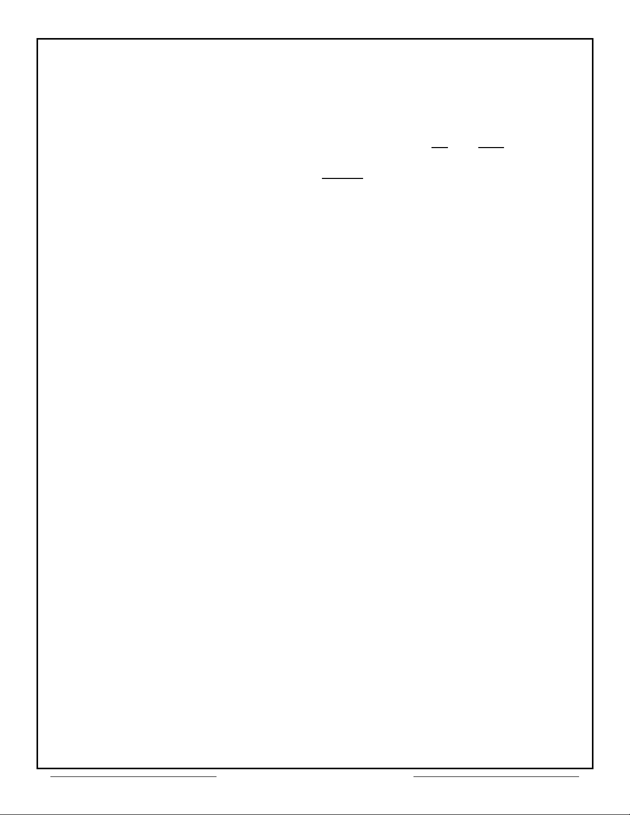
Block Diagram – CQFP(F18)
Standard Configuration
CE1 CE2
RESET
WE
OE
A0 – A20
RY/BY
2Mx8 2Mx8 2Mx8 2Mx8
8 8
I/O0-7 I/O8-15 I/O16-23 I/O24-31
8
Block Diagram – CQFP(F18)
Optional Configuration
RESET
OE
A0 – A20
2Mx8 2Mx8 2Mx8 2Mx8
8 8 8 8
I/O0-7 I/O8-15 I/O16-23 I/O24-31
CE
CE3 WE4WE3WE2WE1 CE1 CE2
Pin Description
I/O
0-31 Data I/O
3
CE4
A
0–20 Address Inputs
WE
CE
OE
RY/BY
RESET Reset
V
8
GND Ground
NC Not Connected
Write Enables
1-4 Chip Enables
Output Enable
Ready/Busy
CC Power Supply
General Description
Utilizing AMD’s Sector Erase
Flash Memory Die, the
ACT-F2M32A is a high speed,
64 megabit CMOS flash
multichip module (MCM)
designed for full temperature
range, military, space, or high
reliability applications.
The ACT-F2M32A consists of
four high-performance AMD
Am29F016 16Mbit (16,777,216
bit) memory die. Each die
contains 8 separately write or
Pin Description
erase sector groups of
256Kbytes (A sector group
I/O
CE4
0-31 Data I/O
A
0–20 Address Inputs
WE
1-4 Write Enable
CE
1-4 Chip Enables
OE
RESET
V
CC Power Supply
GND Ground
NC Not Connected
Output Enable
Reset
consists of 4 adjacent sectors of
64Kbytes each).
The command register is
written by bringing WE
low level (V
and OE
IL), while CE is low
is high (VIH). Reading is
to a logic
accomplished by chip Enable
) and Output Enable (OE)
(CE
being logically active. Access
time grades of 90ns, 120ns and
150ns maximum are standard.
eroflex Circuit Technology - Advanced Multichip Modules © SCD1666A REV A 9/12/97
General Description, Cont’d,
The ACT-F2M32A is packaged in a hermetically sealed co-fired ceramic 68 lead, .94"
SQ Ceramic Gull Wing CQFP package. This allows operation in a military environment
temperature range of -55°C to +125°C.
The ACT-F2M32A can be programmed (both read and write functions) in-system using
the +5.0V V
operations. The end of program or erase is detected by the RY/BY
DQ7, or by the Toggle bit (DQ6).
CC power supply. A 12.0V VPP is not required for programming or erase
pin, Data Polling of
The ACT-F2M32A also has a hardware RESET
pin. When this pin is driven low,
execution of any Embedded Program Alggorithm or Embedded Erase Algorithm will be
terminated.
Each block can be independently erased and programmed 100,000 times at +25°C.
For Detail Information regarding the operation of the Am29F016 Sector Erase Flash
Memory, see the AMD datasheet (Publication 18805).
Aeroflex Circuit Technology SCD1666A REV A 9/12/97 Plainview NY (516) 694-6700
2
Absolute Maximum Ratings
Parameter Range Units
Case Operating Temperature Range
Storage Temperature Range
(1)
Voltage with Respect to GND (All pins except A
Voltage on Pins A
9, OE, RESET
(2)
Vcc Supply Voltage with Respect to Ground
Output Short Circuit Current
Notes:
1. Minimum DC voltage is -0.5V on input/output pins. During Transitions, inputs may undershoot GND to -2.0V for periods up to 20ns. Maximum DC voltage on
input/output pins is V
2. Minimum DC input voltage on A
Maximum DC input voltage on A
3. No more than one output shorted to ground for no more than 1 second.
NOTICE: Stresses above those listed under "Absolute Maximums Rating" may cause permanent damage to the device. These are stress rating only; functional
operation beyond the "Operation Conditions" is not recommended and extended exposure beyond the "Operation Conditions" may effect device reliability.
CC + 0.5V, which may overshoot to VCC + 2.0V for periods up to 20ns.
(3)
9 ,OE, RESET pins is -0.5V. During Voltage transitions, A9, OE & RESET may overshoot GND to -2.0V for periods up to 20ns.
9 is +12.5V which may overshoot to 14V for periods up to 20ns.
9)
(1)
-55 to +125 °C
-65 to +150 °C
-2.0 to +7.0 V
-2.0 to +13.5 V
-2.0 to +7.0 V
200 mA
Recommended Operating Conditions
Symbol Parameter Minimum Maximum Units
CC
V
V
V
T
5V Power Supply Voltage (10%)
IH
Input High Voltage (CMOS)
IL
Input Low Voltage
C
Operating Temperature (Military)
+4.5 +5.5 V
0.7 x V
CC V
+ 0.3 V
cc
-0.5 +0.8 V
-55 +125 °C
Capacitance
(f = 1MHz, TC = 25°C, Standard Configuration)
Symbol Parameter Maximum Units
C
C
C
RESET
C
C
RY/BY
C
C
AD
A0 – A20 Capacitance
OE
OE Capacitance
CE
CE Capacitance
RESET Capacitance
WE
WE Capacitance
RY/BY Capacitance
I/O
I/O0 – I/O31 Capacitance
50 pF
50 pF
20 pF
50 pF
60 pF
50 pF
20 pF
Capacitance Guaranteed by design, but not tested.
DC Characteristics – CMOS Compatible
(TC = -55°C to +125°C, VCC = +4.5V to + 5.5V, Unless otherwise specified)
Parameter Sym Conditions Min Max Units
CC
CC -
10 µA
50 µA
10 µA
160 mA
240 mA
4 mA
4 mA
0.45 V
V
V
Input Load Current
A9 Leakage Current
Output Leakage Current
Vcc Active Read Current
Vcc Active Program/Erase Current
Vcc Standby Current
Vcc Standby Current (Reset)
Output Low Voltage
Output High Voltage
CC Lock-Out Voltage
Low V
Notes:
1. Not 100% tested.
IL
I
VCC = VCCMax., VIN = VCC or GND
LIT
I
VCC = VCCMax., A9 = +12V
LO
I
VCC = VCCMax., VIN = GND to VCC
CC1
I
(1)
I
CC2
CC3
I
CC4
I
OL
V
OH1
V
OH2
V
V
LKO 3.2 4.2 V
= VIL, OE = VIH
CE
= VIL, OE = VIH
CE
CC = VCCMax., CE = RESET = VCC ± 0.3V
V
CC = VCCMax., RESET = VCC ± 0.3V
V
VCC = VCCMin., IOL = 12 mA
CC = VCCMin., IOH = -2.5 mA
V
CC = VCCMin., IOH = -100 µA
V
0.85 x
V
V
0.4V
Aeroflex Circuit Technology SCD1666A REV A 9/12/97 Plainview NY (516) 694-6700
3
 Loading...