

Page 1
AM/FM SIGNAL GENERATORS
2023A, 2023B, 2025
Maintenance Manual
Document part no. 46892/377
Page 2

AM/FM SIGNAL GENERATORS
2023, 2023A, 2023B, 2024 & 2025
Includes information on:
Option 1: No attenuator
Option 2: DC operation
Option 3: High power
Option 4: High stability frequency standard
Option 5: Rear panel connectors
Option 7: Fast pulse modulation
Option 10: 1 V peak mod input
Option 11: Fast pulse and high power
Option 12: SINAD
© IFR Ltd. 1999
No part of this book may be reproduced or transmitted in any form
or by any means, electronic or mechanical, including photocopying,
or recorded by any information storage or retrieval system, without
permission in writing by IFR Ltd.
Printed in the UK
Manual part no. 46882-377
Issue 1
8 March 1999
Page 3

This manual provides servicing information down to a defined circuit area for the 2023, 2023A,
2023B, 2024 and 2025 AM/FM Signal Generators.
Intended audience
The book is intended for qualified service engineers and assumes a knowledge of the instrument to
a level covered in:
Operating Manual 46882-225 for 2023 and 2024
Operating Manual 46882-373 for 2023A, 2023B and 2025.
Structure
Chapter 1 Technical description
This includes block diagrams and detailed board circuit descriptions. The circuit
descriptions refer directly to the servicing diagrams contained in Chapter 7.
Chapter 2 Maintenance
Refer to this chapter for board and unit access, service policy and routine safety
testing and inspection.
Chapter 3 Adjustment procedures
Refer to this chapter for information on password use and adjustment procedures.
Chapter 4 Initial repair
What to do if the instrument shows no signs of life.
Chapter 5 Fault diagnosis
Based on error message reports; narrows the search down to a defined circuit area.
Chapter 6 Replaceable parts
Contains instrument and board component parts, and a section on miscellaneous
mechanical parts.
Chapter 7 Servicing diagrams
Contains interconnection drawings, board circuits and component layout
diagrams.
About this manual
Associated publications
Refer to the relevant Operating Manual (part number 46882-225 for 2023 and 2024, part number
46882-373 for 2023A, 2023B and 2025) for an up-to-date list of associated publications.
ii 46882-377
Page 4

Contents
Precautions......................................................................................................................................................... iv
Précautions........................................................................................................................................................vii
Vorsichtsmaßnahmen
Precauz
Precauciones
Chapter 1 TECHNICAL DESCRIPTION
Chapter 2 MAINTENANCE...........................................................................................................................2-1
Chapter 3 ADJUSTMENT PROCEDURES .................................................................................................3-1
Chapter 4 INITIAL REPAIR .........................................................................................................................4-1
Chapter 5 FAULT DIAGNOSIS ....................................................................................................................5-1
Chapter 6 REPLACEABLE PARTS .............................................................................................................6-1
Chapter 7 SERVICING DIAGRAMS............................................................................................................7-1
ioni .......................................................................................................................................................xiii
.....................................................................................................................................................xvi
Adjustments..............................................................................................................................3-4
Recommended test equipment ................................................................................................3-7
Adjustment procedures............................................................................................................3-8
Adjustment procedures for instruments fitted with Option 3 or 11..................................3-22
Adjustment procedure tables................................................................................................3-24
Appendix A Calibration GPIB commands ........................................................................... A-1
Circuit notes..............................................................................................................................7-2
......................................................................................................................................... x
....................................................................................................1-1
46882-377 iii
Page 5

PRECAUTIONS
Precautions
These terms have specific meanings in this manual:
WARNING
Information to prevent personal injury.
Information to prevent damage to the equipment.
Important general information.
Symbols used on this product
The meaning of hazard symbols appearing on the equipment is as follows:
Symbol Nature of hazard
General hazard
Dangerous voltage
Toxic hazard
Static-sensitive components
General conditions of use
This product is designed and tested to comply with the requirements of IEC/EN61010-1 ‘Safety
requirements for electrical equipment for measurement, control and laboratory use’, for Class I
portable equipment and is for use in a pollution degree 2 environment. The equipment is designed
to operate from an installation category I and II supply.
Equipment should be protected from the ingress of liquids and precipitation such as rain, snow,
etc. When moving the equipment from a cold to a hot environment, it is important to allow the
temperature of the equipment to stabilize before it is connected to the supply to avoid
condensation forming. The equipment must only be operated within the environmental conditions
specified in Chapter 1 ‘Performance data’ in the Operating manual, otherwise the protection
provided by the equipment may be impaired.
This product is not approved for use in hazardous atmospheres or medical applications. If the
equipment is to be used in a safety-related application, e.g. avionics or military applications, the
suitability of the product must be assessed and approved for use by a competent person.
WARNING
Electrical hazards (AC supply voltage)
iv 46882-377
This equipment conforms with IEC Safety Class I, meaning that it is provided with a protective
grounding lead. To maintain this protection the supply lead must always be connected to the
source of supply via a socket with a grounded contact.
Be aware that the supply filter contains capacitors that may remain charged after the equipment is
disconnected from the supply. Although the stored energy is within the approved safety
requirements, a slight shock may be felt if the plug pins are touched immediately after removal.
Page 6
Fuses
Note that the internal supply fuse is in series with the live conductor of the supply lead. If
connection is made to a 2-pin unpolarized supply socket, it is possible for the fuse to become
transposed to the neutral conductor, in which case, parts of the equipment could remain at supply
potential even after the fuse has ruptured.
Removal of covers
Disconnect the supply before removing the covers so as to avoid the risk of exposing high voltage
parts. If any internal adjustment or servicing has to be carried out with the supply on, it must only
be performed by a skilled person who is aware of the hazard involved.
PRECAUTIONS
WARNING
Electrical hazards (DC supply voltage)
This equipment conforms with IEC safety Class III, meaning that for continued safety it must only
be connected to supplies and signal sources which conform to ‘Separated Extra-Low Voltage’
(SELV and SELV-E) voltage and insulation requirements. No hazardous voltages are generated
internally. See under ‘Performance data’ in Chapter 1 of the Operating Manual for the maximum
permitted voltage levels that can be applied.
WARNING
Fire hazard
WARNING
RF hazard
Make sure that only fuses of the correct rating and type are used for replacement.
If an integrally fused plug is used on the supply lead, ensure that the fuse rating is commensurate
with the current requirements of this equipment. See under ‘Performance data’ in Chapter 1 in the
Operating manual for power requirements.
Do not disconnect RF cables which are carrying high levels of RF power. High voltages, which
can cause RF burns, may be present at the end of the unterminated cables due to standing waves.
Switch off the transmitter or other source of RF power before disconnecting the cable from the
equipment.
WARNING
Toxic hazards
WARNING
Beryllia
46882-377 v
Some of the components used in this equipment may include resins and other materials which give
off toxic fumes if incinerated. Take appropriate precautions, therefore, in the disposal of these
items.
Beryllia (beryllium oxide) is used in the construction of the followin g
components in this equipment :
TR808 on AA1 and AA1/1;
TR1 and TR2 on AA2/1 and AA2/7.
Page 7
PRECAUTIONS
This material, when in the form of fine dust or vapor and inhaled into the lungs, can cause a
respiratory disease. In its solid form, as used here, it can be handled quite safely although it is
prudent to avoid handling conditions which promote dust formation by surface abrasion.
Because of this hazard, you are advised to be very careful in removing and disposing of these
components. Do not put them in the general industrial or domestic waste or despatch them by
post. They should be separately and securely packed and clearly identified to show the nature of
the hazard and then disposed of in a safe manner by an authorized toxic waste contractor.
WARNING
Beryllium copper
Some mechanical components within this instrument are manufactured from beryllium copper.
This is an alloy with a beryllium content of approximately 5%. It represents no risk in normal use.
The material should not be machined, welded or subjected to any process where heat is involved.
It must be disposed of as “special waste”.
It must NOT be disposed of by incineration.
Static-sensitive components
The presence of static-sensitive components is indicated in the equipment by yellow disks, flags or
labels bearing the symbol
components being permanently damaged by static charges or fast surges:
1. If a static-sensitive component is to be removed or replaced, the following anti-static
equipment should be used:
• A work bench with a grounded conductive surface.
• Metallic tools grounded either permanently or by repeated discharges.
• A low-voltage grounded soldering iron.
. Certain handling precautions should be observed to prevent these
• A grounded wrist strap and a conductive grounded seat cover for the operator
2. If a printed board containing static-sensitive components (as indicated by warning disk or
flag) is removed, it must be temporarily stored in a conductive plastic bag.
3. As a general precaution, avoid touching the leads of a static-sensitive component. When
handling a new one, leave it in its conducting mount until it is required for use.
4. If using a freezer aerosol in fault finding, take care not to spray programmable ICs as this may
affect their contents.
Suitability for use
This equipment has been designed and manufactured by IFR Ltd. to generate VHF and UHF
signals for the testing of radio communications apparatus. IFR Ltd. has no control over the use of
this equipment and cannot be held responsible for events arising from its use other than for its
intended purpose.
whose outer clothing should not be of man-made fiber.
vi 46882/377
Page 8
Précautions
Les termes suivants ont, dans ce manuel, des significations particulières:
PRECAUTIONS
WARNING
contient des informations pour éviter toute blessure au personnel.
contient des informations pour éviter les dommages aux équipements.
contient d’importantes informations d’ordre général.
Symboles
La signification des symboles liés à cet équipement est la suivante:
Symbole Nature du risque
Risques généraux
Tension dangereuse
Danger produits toxiques
Conditions générales d’utilisation
Ce produit a été conçu et testé pour être conforme aux exigences des normes CEI/EN61010-1
“Règles de sécurité pour appareils électriques de mesurage, de régulation et de laboratoire”, pour
des équipements Classe I portables et pour une utilisation dans un environnement de pollution de
niveau 2. Cet équipement est conçu pour fonctionner à partir d’une alimentation de catégorie I et
II.
Cet équipement doit être protégé de l’introduction de liquides ainsi que des précipitations d’eau,
de neige, etc... Lorsqu’on transporte cet équipement d’un environnement chaud vers un
environnement froid, il est important de laisser l’équipement se stabiliser en température avant de
le connecter à une alimentation afin d’éviter toute formation de condensation. L'appareil doit être
utilisé uniquement dans le cadre des conditions d'environnement spécifiées au chapitre 1
"Performance data" du manuel d'utilisation, toute autre utilisation peut endommager les systèmes
de protection.
Ce produit n’est pas garanti pour fonctionner dans des atmosphères dangereuses ou pour un usage
médical. Si l'équipement doit être utilisé pour des applications en relation avec la sécurité, par
exemple des applications militaires ou aéronautiques, la compatibilité du produit doit être établie
et approuvée par une personne compétente.
WARNING
Sécurité électrique (tension d’alimentation alternative)
!
Cet appareil est protégé conformément à la norme CEI de sécurité Classe 1, c’est-à-dire que sa
prise secteur comporte un fil de protection à la terre. Pour maintenir cette protection, le câble
d’alimentation doit toujours être branché à la source d’alimentation par l’intermédiaire d’une prise
comportant une borne de terre.
Notez que les filtres d’alimentation contiennent des condensateurs qui peuvent encore être chargés
lorsque l’appareil est débranché. Bien que l’énergie contenue soit conforme aux exigences de
sécurité, il est possible de ressentir un léger choc si l’on touche les bornes sitôt après
débranchement.
Fusibles
Notez que le fusible d’alimentation interne est en série avec la phase du câble d’alimentation. Si la
prise d’alimentation comporte deux bornes non polarisées, il est possible de connecter le fusible au
46882-377 vii
Page 9
PRECAUTIONS
neutre. Dans ce cas, certaines parties de l’appareil peuvent rester à un certain potentiel même
après coupure du fusible
Retrait des couvercles
L’appareil doit être débranché avant de retirer les couvercles afin d’éviter tout contact avec les
éléments haute tension. Si toutefois un réglage interne ou une réparation nécessitent la présence
de l’alimentation, ils devront être effectués par une personne qualifiée et avisée des risques
encourus.
WARNING
Sécurité électrique (tension d’alimentation continue)
Cet équipement est conforme aux normes de sécurité CEI Classe III, c’est-à-dire qu’il ne doit être
connecté qu’à des sources d’alimentation ou de signaux qui suivent les recommandations de
tension et d’isolement du type ‘Tension extra-faible séparée’ (SELV at SELV-E). Aucune tension
dangereuse n’est générée en interne. “Performance data” dans le chapitre 1 du manuel
d’utilisation précise les niveaux de tension maximum acceptables en entrée.
WARNING
Risque lié au feu
Lors du remplacement des fusibles vérifiez l’exactitude de leur type et de leur valeur.
Si le câble d’alimentation comporte une prise avec fusible intégré, assurez vous que sa valeur est
compatible avec les besoins en courant de l’appareil. Pour la consommation, reportez-vous au
“Performance data” dans le chapitre 1 du manuel d’utilisation.
Danger RF
Ne jamais debrancher un câble RF connecté à une source de puissance RF en fonctionnement. Il
peut y avoir, à l'extrémité d'un câble non chargé, des tensions très importantes susceptibles de
causer des brûlures graves. Toujours éteindre la source de puissance RF avant de débrancher le
câble sur l'équipement.
WARNING
Danger produits toxiques
Certains composants utilisés dans cet appareil peuvent contenir des résines et d’autres matières qui
dégagent des fumées toxiques lors de leur incinération. Les précautions d’usages doivent donc
être prises lorsqu’on se débarrasse de ce type de composant.
WARNING
Le Béryllia
Le Béryllia (oxyde de Béryllium) entre dans la composition des composants suivants:
TR808 sur AA1 et AA1/1;
TR1 et TR2 sur AA2/1 et AA2/7.
Cette matière peut, lorsqu’elle est inhalée sous forme de vapeur ou de fine poussière, être la cause
de maladies respiratoires. Sous sa forme solide, comme c’est le cas ici, cette matière peut être
manipulée sans risque, bien qu’il soit conseillé d’éviter toute manipulation pouvant entraîner la
formation de poussière par abrasion de la surface.
Il est donc conseillé, pour éviter ce risque, de prendre les précautions requises pour retirer ces
composants et s’en débarrasser. Ne les jetez pas avec les déchets industriels ou domestiques ou ne
les envoyez pas par la poste. Il faut les emballer séparément et solidement et bien indiquer la
nature du risque avant de les céder, avec précautions, à une entreprise spécialisée dans le
traitement de déchets toxiques.
viii 46882/377
Page 10

PRECAUTIONS
WARNING
Bronze au béryllium
Dans cet équipement,certaines pièces mécaniques sont à base de bronze au béryllium. Il s'agit d'un
alliage dans lequel le pourcentage de béryllium ne dépasse pas 5%. Il ne présente aucun danger en
utilisation normale.
Toutefois, cet alliage ne doit pas être travaillé, soudé ou soumis à un processus qui implique
l'utilisation d'une source de chaleur.
En cas de destruction, il sera entreposé dans un container spécial. IL ne devra pas être détruit par
incinération.
46882-377 ix
Page 11
PRECAUTIONS
Vorsichtsmaßnahmen
Diese Hinweise haben eine bestimmte Bedeutung in diesem Handbuch:
WARNING
dienen zur Vermeidung von Verletzungsrisiken.
dienen dem Schutz der Geräte.
enthalten wichtige Informationen.
Symbole
Die Gefahrensymbole auf den Geräten sind wie folgt:
Symbol Gefahrenart
Allgemeine Gefahr
Gefährliche Spannung
Warnung vor giftigen Substanzen
Allgemeine Hinweise zur Verwendung
Dieses Produkt wurde entsprechend den Anforderungen von IEC/EN61010-1
“Sicherheitsanforderungen für elektrische Ausrüstung für Meßaufgaben, Steuerung und
Laborbedarf”, Klasse I transportabel zur Verwendung in einer Grad 2 verunreinigten Umgebung,
entwickelt und getestet. Dieses Gerät ist für Netzversorgung Klasse I und II zugelassen.
Das Gerät sollte vor dem Eindringen von Flüssigkeiten sowie vor Regen, Schnee etc. geschützt
werden. Bei Standortänderung von kalter in wärmere Umgebung sollte das Gerät wegen der
Kondensation erst nach Anpassung an die wärmere Umgebung mit dem Netz verbunden werden.
Das Gerät darf nur in Umgebungsbedingungen wie in Kapitel 1 "Leistungsdaten (Performance
data)" der Bedienungsanleitung beschrieben, betrieben werden; ansonsten wird der vom Gerät
vorgesehene Schutz des Anwenders beeinträchtigt.
Dieses Produkt ist nicht für den Einsatz in gefährlicher Umgebung (z.B. Ex-Bereich) und für
medizinische Anwendungen geprüft. Sollte das Gerät für den Einsatz in sicherheitsrelevanten
Anwendungen wie z.B. im Flugverkehr oder bei militaerischen Anwendungen vorgesehen sein, so
ist dieser von einer für diesen Bereich zuständigen Person zu beurteilen und genehmigen.
WARNING
Elektrische Schläge (Wechselspannungsversorgung)
Das Gerät entspricht IEC Sicherheitsklasse 1 mit einem Schutzleiter nach Erde. Das Netzkabel
muß stets an eine Steckdose mit Erdkontakt angeschlossen werden.
Filterkondensatoren in der internen Spannungsversorgung können auch nach Unterbrechung der
Spannungszuführung noch geladen sein. Obwohl die darin gespeicherte Energie innerhalb der
Sicherheitsmargen liegt, kann ein leichter Spannungsschlag bei Berührung kurz nach der
Unterbrechung erfolgen.
Sicherungen
Die interne Sicherung in der Spannungszuführung ist in Reihe mit der spannungsführenden
Zuleitung geschaltet. Bei Verbindung mit einer zweiadrigen, nicht gepolten Steckdose kann die
Sicherung in der Masseleitung liegen, so daß auch bei geschmolzener Sicherung Geräteteile immer
noch auf Spannungspotential sind.
x 46882/377
Page 12
Abnahme von Abdeckungen
Die Spannungsversorgung muß vor Abnahme von Gehäuseabdeckungen unterbrochen sein, damit
hochspannungsführende Teile gefahrlos zugänglich sind. Falls Abgleiche oder Servicearbeiten
unter Spannung notwendig werden, dürfen solche Arbeiten nur von fachkundigem Personal
durchgeführt werden, das die Gefahren kennt.
PRECAUTIONS
WARNING
Elektrische Schläge (Gleichspannungsversorgung)
Dieses Gerät entspricht der IEC Sicherheitsklasse III. Aus Sicherheitsgründen darf es nur an
Netzgeräte und Signalquellen angeschlossen werden, die in Spannung und Isolation der SELV und
SELV-E Richtlinie genügen (“Getrennte Niederspannung”). Im Gerät werden keine gefährlichen
Spannungen erzeugt. Im Handbuch, Kapitel 1, “Performance data” (Leistungsdaten), werden die
anschließbaren Höchstspannungen definiert.
WARNING
Feuergefahr
Es dürfen nur Ersatzsicherungen vom gleichen Typ mit den korrekten Spezifikationen
entsprechend der Stromaufnahme des Gerätes verwendet werden. Siehe hierzu Kapitel 1
“Leistungsdaten (Performance data)” der Bedienungsanleitung.
WARNING
Hochfrequenzstrahlung
Lösen Sie keine Kabel an welchen größere Pegel von Hochfrequenzleistung anliegen. An den
nichtabgeschlossenen Enden von HF Kabeln können auf Grund von Stehwellen hohe Spannungen
auftreten. Diese verursachen unter Umständen Verbrennungen. Schalten Sie den Sender oder die
Quelle der HF-Leistung vor dem Lösen des HF-Kabels ab.
WARNING
Warnung vor giftigen Substanzen
In einigen Bauelementen dieses Geräts können Epoxyharze oder andere Materialien enthalten sein,
die im Brandfall giftige Gase erzeugen. Bei der Entsorgung müssen deshalb entsprechende
Vorsichtsmaßnahmen getroffen werden.
WARNING
Beryllium Oxid
Beryllium Oxid wird in den folgenden Bauelementen dieses Geräts verwendet:
TR808 auf AA1 und AA1/1;
TR1 und TR2 auf AA2/1 und AA2/7.
Als Staub inhaliert kann Beryllium zu Schädigungen der Atemwege führen. In fester Form kann
es ohne Gefahr gehandhabt werden, wobei Staubabrieb vermieden werden sollte.
Wegen dieser Gefahren dürfen diese Bauelemente nur mit der entsprechenden Vorsicht ausgebaut
und entsorgt werden. Sie dürfen nicht mit Industrie oder Hausmüll vermengt oder per Post
versandt werden. Sie müssen separat verpackt und entsprechend der Gefährdung markiert werden.
Die Entsorgung muß über einen autorisierten Fachbetrieb erfolgen.
46882-377 xi
Page 13

PRECAUTIONS
WARNING
Beryllium Kupfer
In diesem Gerät sind einige mechanische Komponenten aus Berylium Kupfer gefertigt. Dies ist
eine Verbindung welche aus einem Berylliumanteil von ca. 5 % besteht. Bei normaler
Verwendung besteht kein Gesundheitsrisiko.
Das Metall darf nicht bearbeitet, geschweißt oder sonstiger Wärmebehandlung ausgesetzt werden.
Es muß als Sondermüll entsorgt werden.
Es darf nicht durch Verbrennung entsorgt werden.
xii 46882/377
Page 14

Precauzioni
Questi termini vengono utilizzati in questo manuale con significati specifici:
PRECAUTIONS
WARNING
riportano informazioni atte ad evitare possibili pericoli alla persona.
riportano informazioni per evitare possibili pericoli all'apparecchiatura.
riportano importanti informazioni di carattere generale.
Simboli
Significato dei simboli di pericolo utilizzati nell’apparato:
Simbolo Tipo di pericolo
Pericolo generico
Tensione pericolosa
Pericolo sostanze tossiche
Condizioni generali d’uso
Questo prodotto è stato progettato e collaudato per rispondere ai requisiti della direttiva
IEC/EN61010-1 ‘Safety requirements for electrical equipment for measurement, control and
laboratory use’ per apparati di classe I portatili e per l’uso in un ambiente inquinato di grado 2.
L’apparato è stato progettato per essere alimentato da un alimentatore di categoria I e II.
Lo strumento deve essere protetto dal possibile ingresso di liquidi quali, ad es., acqua, pioggia,
neve, ecc. Qualora lo strumento venga portato da un ambiente freddo ad uno caldo, è importante
lasciare che la temperatura all’interno dello strumento si stabilizzi prima di alimentarlo per evitare
formazione di condense. Lo strumento deve essere utilizzato esclusivamente nelle condizioni
ambientali descritte nel capitolo 1 ‘Performance data’ del manuale operativo, in caso contrario le
protezioni previste nello strumento potrebbero risultare non sufficienti.
Questo prodotto non è stato approvato per essere usato in ambienti pericolosi o applicazioni
medicali. Se lo strumento deve essere usato per applicazioni particolari collegate alla sicurezza
(per esempio applicazioni militari o avioniche),occorre che una persona o un istituto competente
ne certifichi l'uso.
WARNING
Pericoli da elettricità (alimentazione c.a.)
Quest ’apparato è provvisto del collegamento di protezione di terra e rispetta le norme di sicurezza
IEC, classe 1. Per mantenere questa protezione è necessario che il cavo, la spina e la presa
d’alimentazione siano tutti provvisti di terra.
Il circuito d’alimentazione contiene dei filtri i cui condensatori possono restare carichi anche dopo
aver rimosso l’alimentazione. Sebbene l’energia immagazzinata è entro i limiti di sicurezza,
purtuttavia una leggera scossa può essere avvertita toccando i capi della spina subito dopo averla
rimossa.
46882-377 xiii
Page 15
PRECAUTIONS
Fusibili
Notare che un fusibile è posto sul filo caldo del cavo di alimentazione. Qualora l’alimentazione
avvenga tramite due poli non polarizzati, è possibile che il fusibile vada a protezione del neutro
per cui anche in caso di una sua rottura, l’apparato potrebbe restare sotto tensione.
Rimozione dei coperchi
Prima di rimuovere i coperchi occorre scollegare la spina d’alimentazione onde evitare il rischio di
esposizione di parti ad alta tensione. Eventuali operazioni di manutenzione che richiedono la
presenza dell’alimentazione dovranno essere eseguite solo da parte di personale specializzato ed a
conoscenza dei pericoli coinvolti.
WARNING
Pericoli da elettricità (alimentazione a c.c.)
Questo strumento rispetta le norme IEC, classe III, e quindi, per una completa sicurezza, deve
essere collegato solo ad alimentatori e generatori di segnali che rispettano I requ isiti d i ten s ione ed
isolamento SELV e SELV-E (Separated Extra-Low Voltage). Nessuna tensione pericolosa è
generata al suo interno. Vedi capitolo 1 del manuale operativo per quanto concerne I livelli
massimi di tensione applicabili.
WARNING
Pericolo d’incendio
Assicurarsi che, in caso di sostituzione, vengano utilizzati solo fusibili della portata e del tipo
prescritti.
Se viene usata una spina con fusibili, assicurarsi che questi siano di portata adeguata ai requisiti di
alimentazione richiesti dallo strumento. Tali requisiti sono riportati nel cap. 1 “Performance data”
del manuale operativo.
WARNING
Rischio a RF
Non sconnettere cavi RF sui quali si stia trasmettendo un segnale RF ad alta potenza. Un'alta
tensione, che può causare bruciature, potrebbe essere presente alla fine di cavi non terminati a
causa delle onde stazionarie. Spegnere il trasmettitore od altra sorgente di segnale RF prima di
disconnettere il cavo dall'apparato.
WARNING
Pericolo sostanze tossiche
Alcuni dei componenti usati in questo strumento possono contenere resine o altri materiali che, se
bruciati, possono emettere fumi tossici. Prendere quindi le opportune precauzioni nell’uso di tali
parti.
WARNING
Berillio
xiv 46882/377
Berillio (ossido di berillio) è utilizzato nella costruzione dei seguenti componenti di
quest’apparato:
Page 16

PRECAUTIONS
TR808 schema AA1 e AA1/1;
TR1 e TR2 schema AA2/1 e AA2/7.
Questo materiale, se inalato sotto forma di polvere fine o vapore, può causare malattie respiratorie.
Allo stato solido, come è usato qui, può essere maneggiato con sufficiente sicurezza anche se è
prudente evitare condizioni che provochino la formazione di polveri tramite abrasioni superficiali.
A cause di questi pericoli occorre essere molto prudenti nella rimozione e nella locazione di questi
componenti. Questi non devono essere gettati tra i rifiuti domestici o industriali né. vanno spediti
per posta. Essi devono essere impacchettati separatamente ed in modo sicuro e devono indicare
chiaramente la natura del pericolo e quindi affidate a personale autorizzato.
WARNING
Rame berillio
Alcuni componenti meccanici in questo strumento sono realizzati in rame berillio. Si tratta di una
lega con contenuto di berillio di circa il 5%, che non presenta alcun rischio in usi normali.
Questo materiale non deve essere lavorato, saldato o subire qualsiasi processo che coinvolge alte
temperature.
Deve essere eliminato come "rifiuto speciale". Non deve essere eliminato tramite "inceneritore".
46882-377 xv
Page 17

PRECAUTIONS
Precauciones
Estos términos tienen significados específicos en este manual:
WARNING
contienen información referente a prevención de daños personales.
contienen información referente a prevención de daños en equipos.
contienen información general importante.
Símbolos
Los significados de los símbolos de peligro que aparecen en los equipos son los siguientes:
Símbolo Naturaleza del peligro
Peligro general
Voltaje peligroso
Aviso de toxicidad
Condiciones generales de uso
Este producto ha sido diseñado y probado para cumplir los requerimientos de la normativa
IEC/EN61010-1 “Requerimientos de la normativa para equipos eléctricos de medida, control y uso
en laboratorio”, para equipos clase I portátiles y para uso en un ambiente con un grado de
contaminación 2. El equipo ha sido diseñado para funcionar sobre una instalación de alimentación
de categorías I y II.
Debe protegerse el equipo de la entrada de líquidos y precipitaciones como nieve, lluvia, etc.
Cuando se traslada el equipo de entorno frío a un entorno caliente, es importante aguardar la
estabilización el equipo para evitar la condensación. Sólo debe utilizarse el aparato en las
condiciones ambientales especificadas en el capítulo 1 “Especificaciones” o “Performance data”
del Manual de Instrucciones/Manual de Operación, en caso contrario la propia protección del
equipo puede resultar dañada.
Este producto no ha sido aprobado para su utilización en entornos peligrosos o en aplicaciones
médicas. Si se va a utilizar el equipo en una aplicación con implicaciones en cuanto a seguridad,
como por ejemplo aplicaciones de aviónica o militares, es preciso que un experto competente en
materia de seguridad apruebe su uso.
WARNING
Nivel peligroso de electricidad (tensión de red)
Este equipo cumple las normas IEC Seguridad Clase 1, lo que significa que va provisto de un
cable de protección de masa. Para mantener esta protección, el cable de alimentación de red debe
de conectarse siempre a una clavija con terminal de masa.
Tenga en cuenta que el filtro de red contiene condensadores que pueden almacenar carga una vez
desconectado el equipo. Aunque la energía almacenada está dentro de los requisitos de seguridad,
pudiera sentirse una ligera descarga al tocar la clavija de alimentación inmediatamente después de
su desconexión de red.
Fusibles
Se hace notar que el fusible de alimentación interno está enserie con el activo del cable de
alimentación a red. Si la clavija de alimentación de red cuenta con sólo dos terminales sin
polaridad, el fusible puede pasar a estar en serie con el neutro, en cuyo caso existen partes del
equipo que permanecerían a tensión de red incluso después de que el fusible haya fundido.
xvi 46882/377
Page 18
Para retirar las tapas
Desconectar de red antes de retirar las tapas para evitar el riesgo que supone tener accesibles
aquellas partes del equipo expuestas a alta tensión. Aquellas operaciones que requieran tener
alimentación con las tapas abiertas para mantenimiento o ajuste deben de ser realizadas por
personal cualificado, que esté al tanto de los riesgos implicados.
PRECAUTIONS
WARNING
Nivel peligroso de electricidad (tensión de alimentación DC)
WARNING
Este equipo cumple con la norma de seguridad IEC clase III, lo que significa que para total
seguridad debe ser conectado a alimentaciones y fuentes de señal que cumplan los requerimientos
de tensión y aislamiento “Tensión Separada Extra-Baja” (SELV y SELV-E). Ninguna tensión
generada internamente implica riesgo para el operario.
En el capítulo 1 “Especificaciones” del Manual de Instrucciones/Manual de Operación podrá
encontrar los valores máximos permitidos que pueden aplicarse.
Peligro de incendio
Asegúrese de utilizar sólo fusibles del tipo y valores especificados como repuesto.
Si se utiliza una clavija con fusible incorporado, aseg úrese de que los valores del fusible
corresponden a los requeridos por el equipo. Ver sección de especificaciones del capítulo 1 del
Manual de Instrucciones/Manual de Operación/Funcionamiento para comprobar los requisitos de
alimentación.
WARNING
Peligro de RF
No desconecte cables de RF que transporten niveles altos de potencia de RF. Es posible la
presencia de altas tensiones, capaces de causar quemaduras por RF, en el extremo del cable sin
terminar, debido a ondas estacionarias. Desactive el transmisor u otra fuente de potencia de RF
antes de desconectar el cable de los equipos."
WARNING
Aviso de toxicidad
Alguno de los componentes utilizados en este equipo pudieran incluir resinas u otro tipo de
materiales que al arder produjeran sustancias tóxicas, Por tanto, tome las debidas precauciones en
la manipulación de esas piezas.
WARNING
Berilio
Berilio (óxido de berilio), se ha utilizado en la fabricación de los siguientes componentes del
equipo:
TR808 en AA1 y AA1/1;
TR1 y TR2 en AA2/1 y AA2/7.
La inhalación de este material, en forma de polvo fino o vapor, entrando en los pulmones, puede
ser causa de enfermedades respiratorias. En forma sólida, como se utiliza en este caso, puede
manipularse con bastante seguridad, aunque se recomienda no manejarlo en aquellas condiciones
que pudieran favorecer la aparición de polvo por abrasión de la superficie.
46882-377 xvii
Page 19

PRECAUTIONS
Por todo lo anterior, se recomienda tener el máximo cuidado al reemplazar o deshacerse de estos
componentes, no tirándolos en basuras industriales o domésticas y no utilizar el correo para su
envío. Deben, ser empaquetados de forma segura y separada, y el paquete debidamente etiquetado
e identificado, señalando claramente la naturaleza del riesgo y ponerlo a disposición de un
destructor autorizado de productos tóxicos.
WARNING
Berilio-cobre
Algunos componentes mecánicos contenidos en este instrumento incorporan berilio-cobre en su
proceso de fabricación. Se trata de una aleación con un contenido aproximado de berilio del 5%,
lo que no representa ningún riesgo durante su uso normal.
El material no debe ser manipulado, soldado, ni sometido a ningún proceso que implique la
aplicación de calor.
Para su eliminación debe tratarse como un "residuo especial". El material NO DEBE eliminarse
mediante incineración.
xviii 46882/377
Page 20

Contents
Chapter 1
TECHNICAL DESCRIPTION
Introduction....................................................................................................................................1-3
Synthesizer..............................................................................................................................1-3
RF processing
LF processing
AA1, AA1/1 RF board
Carrier frequency synthesis
RF board: Carrier generation (sheet 1)
RF board: VCXO loop (sheet 2)
RF board: Synthesizer (sheet 3)
RF board: Loop filter and autocal (sheet 4)
RF board: FM drive (sheet 5)
RF board: Level m
RF board: Frequency generator (sheet 7)
RF board: Interface and attenuator drive (sheet 8)
RF board: Output am
AA2 Attenuator board
Circuit functions
AA2/1 High power attenuator board
Circuit functions
High power attenuator board: Pulse m
High power attenuator board: Power am
AA2/2 Signal output board
Circuit function
AA2/5 Fast pulse m
Circuit functions
Fast pulse m
Fast pulse m
AA2/7 Fast pulse and high power board
Circuit functions
Fast pulse and high power board: Pulse m
Fast pulse and high power board: Attenuator (sheet 3)
Fast pulse and high power board: Power am
AB1, AB1/1 Control board
Introduction...........................................................................................................................
Control board: Microprocessor and m
Control board: DSP audio generator (sheet 2)
Control board: Interrupts and serial interface (sheet 3)
Control board: M
Control board: Standard selection (AB1 sheet 5, AB1/1 sheet 6)
Control board: Interface (AB1 sheet 6, AB1/1 sheet 7)
Control board: PSU filtering and regulation (AB1 sheet 7, AB1/1 sheet 9)
Control board: Power supplies (AB1 sheet 8)
Control board: 31 V dc power supply
AB2 SINAD board
AC1 Backlight inverter board
AF1 Front panel
AC power supply
AC/DC power supply
.........................................................................................................................1-3
..........................................................................................................................1-4
..................................................................................................................1-7
....................................................................................................1-7
...................................................................................1-7
.............................................................................................1-8
..............................................................................................1-9
..........................................................................1-10
...............................................................................................1-12
odulator (sheet 6)....................................................................................1-13
.............................................................................1-14
...............................................................1-16
plifier (sheet 9).................................................................................... 1-18
................................................................................................................1-19
...................................................................................................................1-19
...........................................................................................1-20
...................................................................................................................1-20
od & attenuator (sheet 1)..........................................1-21
p & RPP (sheet 2)................................................. 1-21
.........................................................................................................1-22
.....................................................................................................................1-22
odulator board.............................................................................................1-22
...................................................................................................................1-22
odulator board: Pulse mod (sheet 1).................................................................1-23
odulator board: RPP and atten (sheet 2) ...........................................................1-23
.....................................................................................1-24
...................................................................................................................1-24
od (sheet 2).........................................................1-24
........................................................1-24
p & RPP (sheet 4)........................................... 1-25
.........................................................................................................1-26
1-26
emory (sheet 1).........................................................1-26
......................................................................1-28
........................................................1-30
odulation and level (AB1 sheet 4, AB1/1 sheets 4 & 5)...........................1-34
........................................1-35
........................................................1-36
.........................1-37
......................................................................1-39
(AB1/1 sheet 8)........................................................ 1-39
......................................................................................................................1-39
.....................................................................................................1-39
..........................................................................................................................1-40
.........................................................................................................................1-40
...................................................................................................................1-40
46882-377 1-1
Page 21

TECHNICAL DESCRIPTION
List of figures
Fig. 1-1 Signal generator block schematic...................................................................................1-5
Fig. 1-2 100 MHz phase-locked loop...........................................................................................1-8
Fig. 1-3 Frequency synthesis
g. 1-4 FM/ϕM drive................................................................................................................1-13
Fi
Fig. 1-5 Frequency band selection
Fig. 1-6 Microprocessor and control block diagram
Fig. 1-7 Frequency standard selection
Fig. 1-8 Block diagram
List of tables
Table 1-1: Carrier generation.....................................................................................................1-7
Table 1-2: Attenuator board identification...............................................................................1-11
Table 1-3:
Table 1-4:
Table 1-5:
Table 1-6:
Table 1-7:
Table 1-8:
Table 1-9:
Table 1-10:
Table 1-11:
Table 1-12:
Table 1-13:
Table 1-14:
.....................................................................................................1-10
.............................................................................................1-16
..................................................................1-27
.......................................................................................1-36
of AC/DC power supply module .........................................................1-41
Attenuator control settings......................................................................................1-12
Frequency band selection .......................................................................................1-15
Attenuator selection................................................................................................1-17
Interrupts and chip selects ......................................................................................1-28
Memory bank addressing........................................................................................1-28
Interrupt lines..........................................................................................................1-31
Interrupt lines..........................................................................................................1-31
Latch control lines..................................................................................................1-32
Buffered chip selects ..............................................................................................1-33
Latch control lines..................................................................................................1-33
Buffered chip selects ..............................................................................................1-33
Power supplies........................................................................................................1-40
1-2 46882-377
Page 22

Introduction
The 2023, 2023A, 2023B, 2024 and 2025 AM/FM Signal Generators cover the following
frequency ranges:
9 kHz to 1.2 GHz 2023 and 2023A
9 kHz to 2.05 GHz 2023B
9 kHz to 2.4 GHz 2024
9 kHz to 2.51 GHz 2025
Output levels from -140 dBm to +13 dBm are available. Factory fitted options are available to
extend the level to +25 dBm (+19 dBm above 1.2 GHz) and to provide SINAD measurement
capability. Fig. 1-1 is a block diagram of the frequency synthesis and signal processing circuits.
Synthesizer
A VCXO operating at 100 MHz is phase locked to the internal (or external) frequency standard
using a phase comparator at 10 MHz. The VCXO signal is divided by 20 to give a 5 MHz
reference frequency for the fractional-N loop phase comparator.
A fractional-N loop is used to lock a multiplied low-noise VCO to the reference with a resolution
of l Hz. The VCO tunes from 400 to 535 MHz and is multiplied by three, four or five to yield a
signal in the range 1.2 to 2.51 GHz. A high speed programmable divider is used to divide the
multiplied VCO frequency down to 5 MHz and a phase comparator compares this signal with the
reference derived from the VCXO. The output from the phase comparator corrects the VCO
frequency. In order to provide the required division ratio, the programmable divider is required to
act as a fractional divider. The fractional-N gate array controls the division ratio of the
programmable divider. The variation of this division ratio by the controller enables the loop to
lock, with non-integer division ratios, to the reference with the resolution of 1 Hz without
introducing spurious signals.
FM is produced using a two-point modulation scheme. The FM signal is inserted into the loop by
summing the FM signal with the VCO tune line to modulate the VCO directly. Simultaneously,
the FM signal is fed to the fractional-N controller via a 1-bit oversampled A-D converter which
converts an analogue input into a bit stream of ‘1’s and ‘0’s. The controller uses this input to
modulate the division ratio in sympathy with the modulation. This allows frequencies less than
the loop bandwidth, including DC, to modulate the output frequency.
In order to maintain good FM performance of the two-point modulation system, the VCO FM
tracking characteristics are required to be known. The sensitivity of the FM system via the 1-bit
oversampled A-D converter is VCO independent and accurately calibrated by a DC calibration
system. The VCO tracking is derived by an automatic FM SELFCAL routine during calibration.
During an FM SELFCAL, the error signal on the tune line, for a frequency near the loop
bandwidth, is monitored while varying the FM calibration numbers, allowing the variation in VCO
sensitivities to be calibrated out. This will remove any perturbation of FM flatness near the loop
bandwidth due to mismatch of two modulation paths.
TECHNICAL DESCRIPTION
RF processing
The VCO on board AA1 operates in the range 400 to 535 MHz and feeds to a harmonic generator
whose 3rd, 4th and 5th harmonics are selected by voltage-tuned band-pass filters to pro vide a
frequency in the range 1.2 to 2.4 GHz (2.51 GHz on board AA1/1). To generate frequencies
below 1.2 GHz this signal is divided by factors of two to produce frequencies in the range 10 MHz
to 1.2 GHz. A bank of switched half octave harmonic filters follows which is used to reduce
unwanted harmonics at the output. Then the signal passes through the amplitude modulator where
the output level envelope is controlled. The output from the modulator is peak detected. For
frequencies less than 10 MHz the signal is mixed with an input from the 100 MHz VCXO. The
resulting output in the frequency range 9 kHz to 2.4 or 2.51 GHz is fed from the output amplifier
to attenuator board AA2. For pulse operation the signal is taken to the pulse modulator which
operates in the range 30 MHz to 2.51 GHz. Otherwise the pulse modulator is bypassed and the
signal is fed to the output attenuator. This is controlled by relays and provides attenuation in steps
of 11 dB up to 132 dB. The attenuator also includes an RPP (Reverse Power Protection) system to
protect the instrument from accidental application of reverse power.
46882-377 1-3
Page 23

TECHNICAL DESCRIPTION
LF processing
The LF processing all takes place on control board AB1 or AB1/1, and may be conveniently
subdivided into the following major functional elements.
LF output
A DSP (Digital Signal Processor) is used to generate the audio frequency signals used for internal
modulation. One output from the DSP is used to supply the front panel LF OUTPUT socket.
For external modulation the signal applied to the EXT MOD INPUT socket first passes through
AC/DC coupling selection and then can either be applied directly or via an ALC (Automatic Level
Control) circuit to the audio multiplexers. The external direct signal can also be summed with the
audio frequency from the DSP.
AM and level control
For amplitude modulation the modulation depth is set by a 12-bit A-D converter. A second A-D
converter is used to produce the ALC reference for the RF board. Square law correction is applied
to both signals.
FM/ϕM
For frequency modulation the signal amplitude controls the FM deviation. For phase modulation
the signal is passed through a differentiator circuit.
1-4 46882-377
Page 24

TECHNICAL DESCRIPTION
Fig. 1-1 Signal generator block schematic
46882-377 1-5
Page 25

TECHNICAL DESCRIPTION
1-6 46882-377
Page 26
AA1, AA1/1 RF board
Carrier frequency synthesis
The RF carrier of the instrument should be as clean in frequency (and level) as possible. To
achieve this goal the instrument relies on a single-loop fractional-N Synthesizer scheme and a
harmonic multiplier and UHF oscillator covering the fundamental range from 1.2 to 2.4 GHz
(AA1) or 1.2 to 2.51 GHz (AA1/1). Using this approach minimizes the RF processing circuitry
normally associated with conventional frequency doubling or mixing schemes.
A carrier frequency resolution of 1 Hz cannot be achieved easily without the use of non-integer
division. In this instrument this operation is controlled by a dedicated ASIC which modifies the
division ratio of a programmable divider so that the average frequency is a non-integer division of
the input.
RF board: Carrier generation (sheet 1)
Frequencies from 1.2 to 2.4 GHz (AA1) or 1.2 to 2.51 GHz (AA1/1) are generated by
multiplication from a 400 to 535 MHz low-noise oscillator. The tuned circuit is formed by C102,
C108, varactor diodes D101 to D106 and printed inductors. A maintaining transistor TR101 is
tapped into the tuned circuit. The oscillator is tuned by a differential voltage applied to the
varactor diodes via L101 to L103. The VCO TUNE LOW line is used to phase lock the oscillator
and inject FM whilst the VCO TUNE HIGH line is used to pre-steer the VCO.
The signal from the VCO is buffered by IC101 and then amplified by TR102 to provide a suitable
level to drive the harmonic multiplier. The collector of TR102 is tuned by L104, C114 and C116.
Harmonics are generated by D107 which acts as a step recovery diode. The diode is self-biased to
improve the efficiency of harmonic generation by the network R110, R108 and C111. The
harmonics generated by D107 are filtered by a four stage band-pass filter with a centre frequency
in the range of 1.2 to 2.4 GHz (AA1) or 1.2 to 2.5 GHz (AA1/1). Each filter stage is formed by a
pair of parallel coupled lines. Each line is capacitively loaded at one end by a pair of back-to-back
varactor diodes to allow tuning over an octave. The stages are separated by buffer amplifiers
IC104 to IC107. These amplifiers compensate for the loss and frequency response inherent in
each filter stage and provide isolation so that tuning of the stages is independent. A pad at the
output of each buffer amplifier increases the isolation and provides a better match to the input of
the next filter stage. The filtered signal at the output of IC107 is split by R149 and R150 to feed
the synthesizer dividers (sheet 3) and the output dividers (sheet 7). The filter stages are tuned by a
voltage in the range of 1 to 24 V (AA1) or 1 to 31 V (AA1/1) derived from octal DAC IC103.
This is applied via scaling amplifier IC102a and buffer IC102b. Diodes D125 and D126 allow fast
tuning by shorting out R124 to reduce the charging time constant and so shorten the filter settling
time whenever the frequency is changed. A 1.25 V reference for the DAC is provided by IC108
via IC102c. Table 1-3 below gives the relationship between the VCO frequency, the harmonic
and the final output frequency.
TECHNICAL DESCRIPTION
When the varactor diodes (D108 - D123) need replacing, they must be replaced as a set. If
the alternative type diodes are fitted, resistor R717 will need repositioning accordingly.
Table 1-1: Carrier generation
Output frequency
(MHz)
1200 - 1600 3 400 - 533.3
1600 - 2000 4 400 - 500
2000 - 2510 5 400 - 502
Harmonic number
(N)
VCO frequency
(MHz)
46882-377 1-7
Page 27
TECHNICAL DESCRIPTION
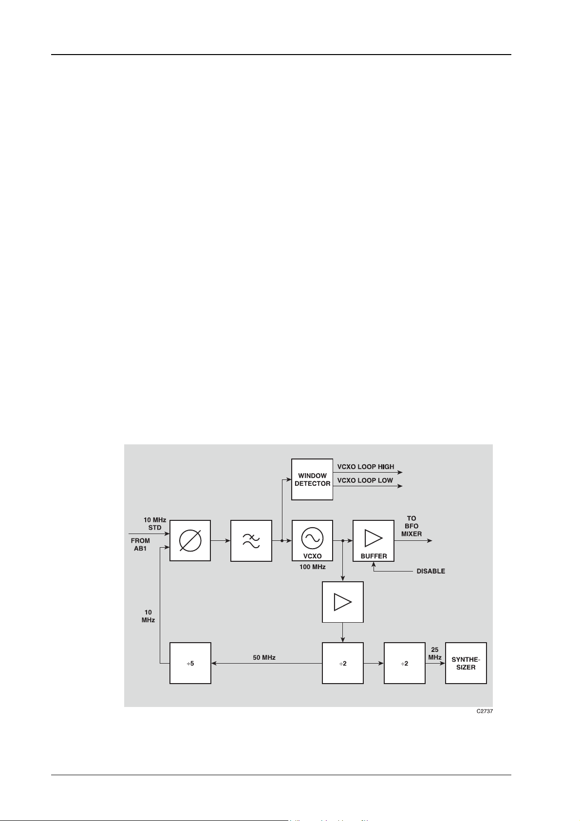
RF board: VCXO loop (sheet 2)
100 MHz VCXO
The 100 MHz VCXO is used to derive all of the clock signals necessary for the fractional-N
Synthesizer. The use of a high frequency eliminates the need for a second phase-locked oscillator
to generate the necessary local oscillator frequency for the BFO. The reference divider provides a
5 MHz clock for the fractional-N Synthesizer and the FM A-D converter.
VCXO operation
The 100 MHz oscillator is built around TR201. Crystal XL201 together with L202 and D201
provide a series resonant circuit in the emitter circuit of TR201. At resonance it increases the gain
of the common-emitter stage and together with 180 degree phase shift network L204, C216, C215,
C219 and C220 connected between the base and collector of TR201 provides the necessary
conditions for oscillation. L203 tunes out the parasitic capacitance of the crystal package and
prevents other spurious oscillations from occurring.
A facility to fine tune the phase shift network is provided by C215. At the resonant frequency, the
circuit operates at maximum power levels when the correct phase shift is achieved around the
transistor. TR202 provides a buffered signal to the VCXO loop divider IC205. A second buffer,
TR203 provides local oscillator drive (at typically +3 dBm) to the BFO mixer (sheet 9). The BFO
DRIVE line to TR204 allows the second buffer amplifier to be powered down when the BFO is
not in use to prevent leakage of the 100 MHz LO onto the instrument output.
100 MHz phase-locked loop
The VCXO is used to provide a reference signal to the fractional-N loop and to the BFO band
mixer and is locked to the 10 MHz frequency standard provided from control board AB1 or AB1/1
via PLAB. The buffered 100 MHz signal is divided down to 10 MHz before phase comparison.
An integrator and active low-pass filter ensures the removal of the reference frequency from the
VCXO tune line. A window comparator monitors the VCXO tune line to detect when the
oscillator is outside its normal operating range. The block diagram of the phase-locked loop is
shown in Fig. 1-2.
Fig. 1-2 100 MHz phase-locked loop
1-8 46882-377
Page 28

Loop operation
The 100 MHz signal from the VCXO is buffered and amplified by TR205 to yield a CMOS logic
compatible signal for the dividers which follow. The signal is divided by two by IC205a and then
by five by IC202 to give 10 MHz for phase comparison. IC201 and IC203 form the loop
phase-frequency comparator. R203 and C208 remove the fast edges from the output of the phase
detector. A broken integrator is formed around IC204b. This has a break frequency of 80 Hz and
a gain at high frequency of four. IC204a, which follows, is a second-order active low-pass filter
with a cut-off of 700 Hz and a gain of two. The resulting loop bandwidth is approximately
150 Hz. The output from the active low-pass filter is further filtered by R212 and C213 to remove
any high frequency signals.
IC204c and d form a window comparator which detects when the VCXO tuning voltage range is
exceeded. The outputs from the comparators are attenuated to logic levels by R216 to R219 to
give VCXO LOOP HIGH and VCXO LOOP LOW lines to provide status interrupts to the main
processor via IC704 (sheet 8).
RF board: Synthesizer (sheet 3)
Synthesizer operation
Frequency synthesis control is performed by a dedicated ASIC, IC305. This generates all of the
necessary division ratios for programmable divider IC307 to synthesize any frequency within the
range 1.2 to 2.4 GHz (AA1) or 1.2 to 2.51 GHz (AA1/1). Synthesizer operation is summarized in
Fig. 1-3.
The 1.2 to 2.51 GHz (AA1) or 1.2 to 2.51 GHz (AA1/1) input signal from the harmonic generator
(sheet 1) is buffered by TR305 (sheet 3) to prevent divider spurious signals from IC309 reaching
the instrument output. Signal feedback is not used with this stage, to give high reverse isolation.
The buffered signal is divided by two by IC309 and then amplified by IC308 to obtain a sufficient
level to drive the input of programmable divider IC307. The programmable divider is used to
provide integer division in the range 120 to 240. Fractional division is achieved by the
modification of the integer division ratios, under the control of ASIC IC305, in such a way that the
average frequency over time is not an integer division ratio of the original. Control inputs to
IC307 are TTL compatible. The control outputs from ASIC IC305 are inverted by IC306 to
provide the correct polarity for IC307. Resistors R316 to R323 and R343 to R350 reduce the
amplitude of the control signals to 2.5 V. The outputs of IC307 are converted from ECL to TTL
levels by differential pair TR302 and TR303 and a single-ended amplifier TR304. Diode D307
provides Schottky clamping for TR304 to ensure fast switching. The signal on the collector of
TR304 is an all active edge squarewave at a 2.5 MHz rate. The fractional control ASIC and phase
detector both require a clock with active positive edges. IC310d converts the 2.5 MHz signal to a
5 MHz signal with a short duty cycle and an active positive edge. The remaining gates of IC310
provide buffering. The division ratio generated by ASIC IC305 will be modified every time a
positive edge is received at pin 51.
The reference for the main loop is obtained by dividing the 25 MHz signal present at IC302 pin 2
by five. The output of IC302 pin 11 is a 5 MHz rate pulse with a duty cycle of 40 ns. The clock
for the 1-bit oversampled A-D converter is obtained from IC302 pin 13 after buffering and
inversion by IC303a. The reference and divided output signal are compared by a phase frequency
comparator comprising IC311, IC312b and IC313a. The phase detector output to the loop
integrator and filter is available on pin 12 of IC311d. Under normal phase lock this will be a
5 MHz squarewave with nearly 50% duty cycle.
TECHNICAL DESCRIPTION
1-bit A-D converter
The DC input path to the Synthesizer consists of a third-order, single-bit, oversampling A-D
converter, whose bit stream output is used to dynamically control the Synthesizer frequency via
the Synthesizer ASIC.
46882-377 1-9
Page 29
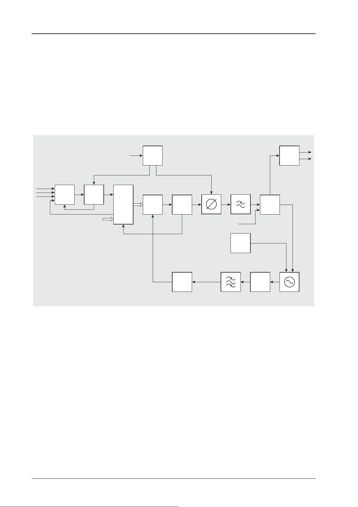
TECHNICAL DESCRIPTION
Pin 6 of IC301b is used as the summing junction for four currents. These are: the input current
from control board AB1 or AB1/1 via R307 and R352; a negative offset current via R306; the bit
stream feedback via R310; and the DC nulling offset current via R311. IC301b integrates the sum
of these currents, and its output is further integrated by broken integrators IC301c and d. In these,
when the frequency rises to a point where C301 and C302 are at low impedance, the ICs act as
unity-gain amplifiers. Diodes D301 to D304 are used to enable the converter to recover cleanly
from an overload.
The output from the last integrator is fed via comparator TR301, which converts the input to TTL
levels, to D-latch IC304a, which is clocked at the same rate as the Synthesizer ASIC. The output
from the D-latch is fed back into the summing junction to close the converter control loop. The
output from IC304a is a pseudo random bit stream that represents the analogue FM input to
IC301b. The bit stream is used by the Synthesizer ASIC to control the main carrier frequency.
BIPOLAR
OFFSET
FM/FM
DC
NULLING
OFFSET
S
5 MHz
1-BIT
ADC
CONTROL
DATA
FRACTIONAL
CONTROLLER
CLK
FROM
VCXO
25 MHz
REF
DIV
5¸
DIVIDE
BY N
COUNTER
600-1200 MHz (AA1)
600-1255 MHz (AA1/1)
MHz
FN
LOOP
HIGH
WINDOW
COMPARATOR
5 MHz
2.5
x2
5 MHz
2¸
1.2-2.4 GHz (AA1)
1.2-2.51 GHz (AA1/1)
FM ATTEN
VCO
PRE- STEER
VCO TUNE HIGH
HARMONIC
GENERATOR
S
VCO
VCO
TUNE
LOW
FN
LOOP
LOW
C4438
Fig. 1-3 Frequency synthesis
The DC nulling offset current is supplied from a 1-bit oversampling D-A converter in the
Synthesizer ASIC. This balances the input current to make the converter read zero when DC
nulling and when in AC coupled FM mode.
RF board: Loop filter and autocal (sheet 4)
Loop filter
The input on the PHASE DETECTOR line is filtered by R404 and C401 to remove fast edges
before the signal reaches loop integrator IC402. The loop integrator has a break frequency set by
C402 of approximately 1.5 kHz and gain at high frequency of 1.2. The network R414, R415,
C405 and C406 provides rejection of unwanted noise in the 10 to 30 kHz range without
introducing a large phase shift at the loop bandwidth. IC404 is a unity gain second-order active
low-pass filter with a cut-off frequency of 40 kHz. The filtered signal from IC404 is attenuated
and summed with the FM drive signal on the FM ATTEN line by R433. This results in the VCO
TUNE LOW output to the VCO (sheet 1). Loop bandwidth is approximately 3 kHz.
1-10 46882-377
Page 30

Correct phase lock is monitored by IC406c and d which detect when the voltage at the output of
IC406a exceeds ±8 V. Hysteresis is provided by R443 and R444. The detected outputs from
D408 and D409 on the FN LOOP HIGH and FN LOOP LOW lines are attenuated to logic levels
by R449 to R452. Loss of phase lock is signaled by interrupting the main processor via IC703 and
IC704 (sheet 8).
VCO pre-steer
The VCO PRE-STEER voltage is generated by octal DAC IC103 (sheet 1). The signal from the
DAC is amplified by IC401a and b to provide a tuning voltage in the range 1 to 22 V.
Temperature compensation for the VCO is provided by D414. Under normal operation the presteer voltage is filtered by R423 and C411 to prevent noise injection onto the VCO tune line.
Diode D415 and IC408 allow fast tuning by shorting out R423 to reduce the charging time
constant. IC408 is only switched on using the PRE-STEER SWITCH line during frequency
changes that involve updating the pre-steer voltage.
Autocalibration
Dedicated hardware has been added to the Synthesizer to allow fast automatic calibration of the
VCO pre-steer and FM frequency response. Pre-steer calibration is achieved by minimizing the
loop error voltage present at the output of IC406a. This is achieved by IC406b which forms a
simple zero-crossing detector.
The FM frequency response calibration is performed by applying FM to the carrier with a 2 kHz
modulating tone. Calibration is performed by minimizing the amplitude of the resulting 2 kHz
tone present at the output of the loop filter. The magnitude of the FM drive voltage applied to the
VCO is adjusted automatically whilst the phase relationship between the loop error tone and the
applied modulating tone is monitored. The correct drive level is found at the point where the
phase switches from being in phase to being out of phase. IC407a is used to amplify the loop
error tone. TR402 and C417 are used to implement a crude charge pump phase detector. IC407d
is used to clip the 2 kHz modulating tone so that TR402 gate is driven with a squarewave. The
output from the phase detector is filtered by two RC sections and buffered by IC407b. The sign of
the filtered voltage, and hence the point of phase reversal is monitored by IC407c. The output of
IC407c is converted to logic levels by D412, R457 and R458. Forward biasing D404, D405,
D411 and D413 using the CAL DISABLE line suppresses the operation of the autocalibration
hardware.
TECHNICAL DESCRIPTION
AA2 board identification
The AA2 BOARD SENSE line indicates one of three conditions to the processor: a standard
attenuator board AA2 is fitted; a high-power attenuator board AA2/1 is fitted ; no attenuator is
fitted. PLAE 15 indicates these conditions respectively by being: shorted to earth; open circuit;
connected to earth via a 1 kΩ resistor. The two output lines BOARD ID (A) and BOARD ID (B)
are connected by pull-up resistors R723 and R724 to IC705 (sheet 8). The logic is shown in Table
1-2. below.
BOARD ID
Board type PLAE 15 TR406 TR407 (A) (B)
Standard Shorted to
High power Open circuit ON ON L L
No attenuator Resistor ON OFF L H
Table 1-2: Attenuator board identification
OFF OFF H H
earth
46882-377 1-11
Page 31

TECHNICAL DESCRIPTION
Power amp cal comparator
Comparator IC401c compares the power amplifier detector level output from high power
attenuator board AA2/1 with the POWER AMP CAL signal on IC401c pin 10. The latter signal
comes from DAC IC103 (sheet 1). The comparator circuit performs a dual function. In
instrument calibration mode the AA2/1 detector output is calibrated using the POWER AMP CAL
signal to find the ‘trip level’, when the POWER AMP CAL output changes state. In normal
instrument operation the high power DAC signal is set 6 dB below the expected detector level.
Then, if due to some failure the power amplifier output falls by more than 6 dB, POWER AMP
CAL will flag an error, resulting in an error message being generated on the screen.
RF board: FM drive (sheet 5)
FM adjusts the instantaneous RF frequency in direct sympathy with the modulating signal. The
amount of frequency deviation is directly proportional to the magnitude of the modulation source.
With phase modulation the frequency deviation is also proportional to the frequency of
modulation.
For moderate modulation rates the signal is injected straight onto the VCO tune line after suitable
scaling by D-A converters (giving fine control) and fixed attenuators (giving coarse control). The
block diagram of the FM drive is shown in Fig. 1-4.
Inside the loop bandwidth this method is not valid as the loop cannot distinguish between FM and
other VCO frequency errors. It would therefore try to compensate for the modulation tone by
returning the carrier back to the original requested frequency. A digital system is used to
overcome this effect, which also has the benefit of extending the modulation range down to DC.
The modulation is sampled by a 1-bit oversampling A-D converter whose output controls the
Synthesizer gate array controller ASIC in such a way as to offset the carrier frequency in
proportion to the magnitude of the modulation. The speed at which the ASIC can perform this
function sets a limit to the overall bandwidth of the system. At frequencies above the loop
bandwidth the analogue system dominates.
Operation
The FM input to the RF module feeds the 1-bit oversampling A-D converter and the analogue FM
attenuator. The analogue attenuator provides the FM drive signal to the VCO and consists of two
stages. A 12-bit multiplying D-A converter, IC409, allows fine setting of the FM drive level.
Coarse setting is achieved by IC403 and by a pad switched by RLA. IC403 is an analogue
multiplexer; it is used to provide attenuation of 0, 20 or 40 dB, and can be used to connect the FM
input to ground. IC405a has 10 dB of gain and provides a high current drive for the final
attenuator stage. The final attenuator stage is switched by RLA and gives either 10 or 50 dB of
attenuation. The output from the final attenuator stage on the FM ATTEN line is summed with the
control voltage from the fractional-N loop across R431 and R432 (sheet 4) which provides a
25 Ω
drive to the VCO. The FM attenuator control settings are given in Table 1-3.
Table 1-3: Attenuator control settings
Atten (dB) AT2 AT1 AT0
OFF 0 0 0
20 1 0 0
40 1 1 0
60 0 1 0
80 0 1 1
1-12 46882-377
Page 32

TECHNICAL DESCRIPTION
VCO FM tracking autocalibration is performed by IC407 and associated circuitry (see
‘Autocalibration’ above for details). Digital FM and FM at low modulation frequencies is
achieved by the combination of the 1-bit oversampled A-D converter formed by IC301, IC304a
and synthesizer ASIC IC305 (sheet 3). The A-D converter samples the modulation source at a
high rate and passes the information to the gate array controller in a high speed serial data stream.
The ASIC then modifies the control to the main divider IC307 to change the instantaneous
frequency of the carrier.
RF board: Level modulator (sheet 6)
Amplitude modulator
The amplitude modulator is responsible for applying amplitude modulation to the carrier. To do
this a voltage-controlled pin diode modulator and envelope detector are used in a control loop to
apply amplitude modulation to the RF carrier. The control voltage from the control board is
predistorted before it is applied to the control loop to compensate for the inherent non-linearity of
the Schottky diode detector used for envelope detection.
PIN modulator
Diodes D501 to D507 are the pin diodes arranged as a dual π modulator. Transistors TR501 and
TR502 form a pair of voltage-controlled current sinks which produce complementary output
currents, one to drive the series diodes and one to drive the shunt diodes. Resistor R513 sets the
transconductance of these current sinks and hence the gain of the pin modulator. Capacitor C523
across R513 helps to speed up the modulator by providing lead compensation for the pin diodes;
the time constant of R513 and C523 being approximately equal to the charge lifetime of the pin
diodes. Resistors R509 and R511 are required to source current into the diodes when stored
charge needs to be removed quickly from the diodes since internal recombination alone is far too
slow.
Transistors TR506 and TR510 are two similar RF amplifying stages. TR506 recovers losses from
the pin modulator and TR510 recovers losses from the divider and filter stages (sheet 7). Since the
same DC biasing is used for both stages only one stage, that for TR506, will be described.
Resistors R516 and R542 fix the base voltage on TR503 which in turn sets the collector voltage on
TR506. The collector current is set by the value of R524. A two-inductor combination, L505 and
L506, is used to isolate the RF line from the DC circuitry. Diode D515 compensates for the
Fig. 1-4 FM/
ϕ
M drive
46882-377 1-13
Page 33

TECHNICAL DESCRIPTION
TR503 base-emitter variations with temperature. Resistors R521, R546, R547 and R555, R556 set
the RF gain of this stage.
The control voltage input to the modulator is converted into a digital word by an analogue to
digital converter. This converter is implemented with comparator IC501a and FILTER CAL from
one of the DACs in IC103, the status of the comparator being available as FILTER PEAK. This
measurement is used for self-calibration of the voltage-tuned band-pass filters on sheet 1 and also
for instrument fault diagnosis.
Peak detector and control loop
D510 is the Schottky detector diode used to detect the peak RF voltage on the microstrip line. The
output from this detector is not linear at low RF levels but obeys a square law transfer function,
hence if modulation distortion is to be eliminated, the control voltage from the control board must
compensate for this effect. Schottky diode D511 is used for temperature compensation of D510.
The modulation voltage on the AM INPUT line from control board AB1 or AB1/1 is larger than
that required by the control loop and is attenuated by R527 and R517. The voltage level from the
control board is approximately 1.4 V average with the modulation superimposed on it. An error
amplifier consisting of IC802a amplifies the differential error voltage between the modulation
input and the detector output. The output of this error amplifier then controls the pin modulator as
necessary to keep the error voltage as small as possible. Feedback in the form of C511 and R526
reduces the effective gain and phase shift of the error amplifier at high frequencies to ensure
adequate gain and phase margins.
Level modulator
The level modulator is based around PIN diodes D512 and D513 and is split into two sections with
amplifier stage TR508 in between. The input level to the modulator is nominally -4 dBm
(10 MHz to 2.4 GHz), and it has an inherent loss of up to 3 dB. The modulator diodes are
controlled by the LEVEL MOD input line from leveling loop integrator IC802 (sheet 9). The loop
integrator input (in the range ±10 V) sets the amount of current through diode packages D512 and
D513 by controlling TR504 and TR505 collector current levels. When D512 and D513 pins 1 are
at -10 V the two series diodes are fully ON and the shunt diode is reverse biased, resulting in
minimum RF signal loss (low attenuation limit). When D512 and D513 pins 1 go positive with
respect to pins 3 and 4, the two series diodes become reverse biased and the shunt diodes forward
biased resulting in maximum RF signal loss in the modulator (high attenuation limit). TR507 sets
the DC biasing condition for TR508.
Output unleveled
The comparator configuration around IC501b detects the condition where the level modulator
drive signal gets close to the positive supply rail value. It compares the LEVEL MOD input with
the +11 V supply, and signals on the OUTPUT UNLEVELED line that the level modulator is
close to or at the minimum attenuation limit and therefore the output may be unleveled.
Pulse modulation drive
The pulse modulator driver is based around IC503a and is basically a level translating buffer stage.
The input on the PULSE I/P line from control board AB1 or AB1/1 to the driver is at TTL levels.
The output is clamped by zener diodes D508 and D509 at approximately ±8 V. When the input is
LOW (0 V) the output is at -8 V and when the input is HIGH (+5 V) the output is at +8 V. The
output on the PULSE O/P line drives the pulse modulator on attenuator board AA2. When the
pulse signal input is LOW, the pulse modulator goes into low isolation (RF ON) mode and vice
versa.
RF board: Frequency generator (sheet 7)
Frequency generation
A UHF VCO, step recovery diode and voltage tuned band-pass filter (sheet 1) are used to g en erate
a fundamental octave between 1.2 and 2.4 GHz which is phase locked to the instrument reference.
1-14 46882-377
Page 34

To generate frequencies below 1.2 GHz, a fixed ÷2 prescaler and a programmable ÷2n prescaler
(on this sheet) are used to divide the input frequency of 1.2 to 2.4 GHz down to frequencies
between 10 MHz and 1.2 GHz. Switched low-pass filters (LPF) are then used to reduce unwan ted
harmonics at the output. To produce frequencies between 9 kHz and 10 MHz, the 100 MHz
instrument reference is mixed with the divider generated signal of between 100 MHz and
110 MHz to produce a beat note below 10 MHz (sheet 9).
Frequency band selection
A serial communications link between the RF board and control board AB1 or AB1/1 is used to
control the operation of the RF board. Data latch IC709 (sheet 8) converts the serial data input
from the control board into the parallel control bits required to select a particular frequency band.
Frequency band selection is shown in Fig. 1-5.
Four control bits (BS0 to BS3) are required to specify the required frequency from the dividers
and filters. Control bit BS0 selects the upper or lower ½ octave but is only required for selected
frequencies between 300 MHz and 1.2 GHz and is set to zero for selected frequencies outside
these limits (BS0 is set high for the lower ½ octave). Control bits BS1 to BS3 select the required
octave of output frequency from the dividers. Table 1-4 below lists the control bits required for
the selection of each frequency band.
TECHNICAL DESCRIPTION
Table 1-4: Frequency band selection
1.2-2.51 GHz
FROM
FREQUENCY
MULTIPLIER
BS3 BS2 BS1 BS0 Selected band
0 0 0 0 420 - 600 MHz
0 0 0 1 300 - 420 MHz
0 0 1 0 150 - 300 MHz
0 1 0 0 75 - 150 MHz
0 1 1 0 37.5 - 75 MHz
1 0 0 0 18.75 - 37.5 MHz
1 0 1 0 10 - 18.75 MHz
1 1 0 0 1.2 - 2.51 GHz
1 1 1 0 0.84 -1.2 GHz
1 1 1 1 600 - 840 MHz
This particular mapping enables these same control bits to be used for LPF selection as well as to
control the division ratio of IC602 which is a programmable divider. IC603 and IC608 are each
three to eight line decoders which produce a logic low level on the particular output specified by
the band selection bits, all other outputs remaining high. Each of the decoder outputs corresponds
to one particular signal path which is switched in with pin diodes. These pin diodes cannot
operate directly with standard logic levels so IC604 to IC606 convert the logic level outputs of
IC603 and IC608 into the required levels for driving the pin diodes.
¸2
PRESCALER
n
¸2
PRESCALER
10 MHz-2.51 GHz
TO AMP MOD
840 MHz 420 MHz
1200 MHz
600 MHz
<600 MHz
37.5 MHz 18.75 MHz
300 MHz
150 MHz
75 MHz
C4439
46882-377 1-15
Page 35

TECHNICAL DESCRIPTION
Fundamental octave
The 1.2 to 2.4 GHz from the voltage tuned band-pass filter (sheet 1) is the fundamental octave and
is amplified by IC607 to ensure adequate drive for the subsequent circuitry. When a frequency
within this fundamental octave is selected, the 1.2 to 2.4 GHz switch is selected by the SW1
control line going negative. Diodes D603 to D605 are then reverse biased whilst a half each of
diodes D601 and D602 are forward biased. Hence the prescalers and sub 1.2 GHz filters are
bypassed.
600 MHz to 1.2 GHz generation
IC601 is a fixed ÷2 prescaler used to divide the fundamental octave down to between 600 MHz
and 1.2 GHz. TR606 and R636 are used to bias IC601 off when not required, this prevents IC601
from self-oscillating. TR601 is selected whenever one of switch lines SW2 to SW10 is low,
TR601 being used to detect this condition, switch TR606 off as required and hence enable IC601.
The output level of this prescaler is not high enough to drive programmable prescaler IC602
directly, so TR603 and TR604 form a balanced amplifier to boost the output level. When
600 MHz to 1.2 GHz is selected, balun T601 transforms the amplified balanced output of IC601
into an unbalanced output appropriate for microstrip, D607 being used to connect one output of
T601 to ground.
The 600 MHz to 1.2 GHz octave is split into two half-octaves because the second-harmonic
content of the output is too high to allow octav e filtering.
The 1200 MHz LPF is permanently in place for frequencies below 1.2 GHz, and a simple switch
consisting of D608 to D612 is used to route the output of T601 through to the 1200 MHz filter.
The sub-840 MHz half-octave path switch is similar but also contains the 840 MHz LPF.
Fig. 1-5 Frequency band selection
Programmable divider
IC602 is the programmable divider which is used to produce frequencies down to 10 MHz. This
divider is only useable up to 1.5 GHz, hence the need for prescaler IC601 which is useable to at
least 2.5 GHz. The required division ratio is set by control bits BS1 to BS3 and represents a
power of 2. The division ratio selected is related to the selection bits by the following expression:
Division ratio = 2
The output of IC602 is balanced and is converted to a single ended output by balun T602 which is
identical to T601. The output level of this divider is already high enough not to require any extra
amplification. For frequencies below 300 MHz, the output is balanced well enough to require
only octave filtering thereby reducing the number of filters required to meet the harmonic
performance requirement. Between 300 MHz and 600 MHz however, two half octave filters are
used. D606 and R635 are required to short out the 600 MHz LPF when the 840 MHz filter is
selected to prevent D615 from resonating with the 600 MHz filter.
[(4×BS3)+(2×BS2)+BS1+1]
RF board: Interface and attenuator drive (sheet 8)
Serial bus interface
The serial bus from control board AB1 or AB1/1 is connected to PLAC and fed to serial to parallel
converters IC702 and IC706. These ICs supply address and data information to the fractional-N
controller (sheet 3) and data to decoder IC707. The outputs from IC707 provide clock signals to
parallel to serial converters IC708 to IC710 and enable signals to IC704 and IC705. AT0 to AT2
from IC708 select the FM drive fine setting. IC709 provides parallel control bits BS0 to BS3 used
for frequency band selection.
IC704 and IC705 perform parallel to serial conversion for the transmission of board status signals
to the processor. IC705 is monitored by the processor, and when OR-gate IC703 detects a fault
condition, for example, RPP TRIPPED going high, the processor is aware of a fault condition but
does not know what the fault is. It then performs a serial poll of the inputs to IC704 to determine
the actual fault.
1-16 46882-377
Page 36

Attenuator drive
The attenuator pad data comes via the serial bus and is latched by serial-to-parallel converter latch
register IC710. When a pad control line output is LOW (0 V) the corresponding attenuator pad is
selected via one of the transistor switches TR701 to TR707. Conversely when the latch output
goes HIGH (+5 V) the pad is deselected. There are five attenuator pads which need controlling,
they are labeled PAD A (33 dB), PAD B (22 dB), PAD C (33 dB), PAD D (11 dB) and PAD E
(33 dB). This gives a total attenuation of 132 dB, selectable in 11 dB steps. The pad control lines
can source up to 200 mA. The pad selection combinations for any required attenuation setting are
shown in Table 1-5 below.
Attenuation A (33 dB) B (22 dB) C (33 dB) D (11 dB) E (33 dB)
0 1 1 1 1 1
11 1 1 1 0 1
22 1 0 1 1 1
33 1 1 1 1 0
44 1 1 1 0 0
55 1 0 1 1 0
66 1 1 0 1 0
77 1 1 0 0 0
88 1 0 0 1 0
99 1 0 0 0 0
110 0 1 0 0 0
121 0 0 0 1 0
132 0 0 0 0 0
TECHNICAL DESCRIPTION
Table 1-5: Attenuator selection
Pulse modulation
There are two control lines related to pulse modulation, one is the PULSE I/P line (sheet 6) which
comes from the rear panel via control board AB1 or AB1/1 and the other is the PULSE MOD
ENABLE line obtained by decoding the serial bus. When the output is LOW the pulse modulator
path is selected. Conversely, when the output is HIGH, the straight-through path is selected and
the pulse modulator is set to low isolation mode (pulse input set LOW). This line is capable of
sourcing 200 mA.
RPP control
The Reverse Power Protection (RPP) circuit has two lines on this board. The RPP TRIPPED
readback line from attenuator board AA2 is normally LOW and goes HIGH when the RPP has
tripped. The RPP RESET control line is normally HIGH and switched LOW (for less than 1 ms)
to reset the RPP relay.
High power amplifier option
The high power amplifier, when fitted, is switched on attenuator board AA2 by a single control
line from this board. When the HIGH POWER ENABLE control line is LOW the amplifier is
selected and when HIGH it is deselected.
46882-377 1-17
Page 37

TECHNICAL DESCRIPTION
RF board: Output amplifier (sheet 9)
Output amplifier
The output amplifier consists of four, common-emitter, transistor stages (TR806 to TR808 and
TR814). The first two stages are only used down to 10 MHz and are switched OFF to obtain high
isolation below 10 MHz. Frequencies between 10 kHz to 10 MHz are obtained by mixing the
input with a 100 MHz local oscillator. The switching between these two paths from the
MODULATED RF input is controlled by the BFO SELECT line. When this line is in LOW state,
TR810 is OFF and TR811 is ON and the corresponding transistors TR801 to TR803 are ON and
TR804 and TR805 are OFF. In this state transistors TR801 and TR802 set the RF transistors
TR806 and TR807 in amplifying mode and TR805 sets TR812 in isolation mode. Transistors
TR803 and TR804 set D801 bias by forward biasing the diode between pins 1 and 4 and reverse
biasing the diode between pins 1 and 3, thereby selecting the high frequency path via C806.
Conversely, when the BFO SELECT line goes HIGH, the high frequency path is set to isolation
mode and the BFO low frequency path via C802 is selected. Since all four transistor amplifier
stages have similar active biasing arrangements, only the final stage will be described here.
Resistors R847 and R848 and diode D808 fix the base of TR809. TR809 in turn forward biases
TR808 base-emitter junction until TR809 collector is one diode drop above the base potential.
L808 has about 15 Ω winding resistance, and with R849 and R875 also set to 15 Ω, the TR808
collector current is approximately 110 mA with 16 V across it. Note that diode D808 is only
added to temperature compensate the base-emitter junction voltage. Below 10 MHz the BFO path
is selected and TR806 and TR807 are switched OFF; this results in D802 being reverse biased
through R839. This increases the isolation of the straight-through path.
The lead dimensions of leaded capacitor and resistor components are critical to the
instrument’s performance. Make sure these components are replaced in identical fashion.
BFO-band frequency generation
Transistors TR815 to TR820 are configured as a double-balanced Gilbert cell mixer. The resistors
improve the noise performance because the transconductance of the upper switching transistors is
now limited by the resistors instead of increasing with the bias current. Hence the signal handling
capability of the mixer can be improved, by increasing the bias current, without increasing the
output noise. The disadvantage with this is that the local oscillator (LO) signal must now be larger
to overcome the increased voltage drop across these resistors.
An LO level of 0.5 V is adequate to guarantee complete switching of the balanced signal currents
from TR819 and TR820. The LO signal is derived from the 100 MHz internal reference on sheet
2, hence the input RF frequency to the mixer should be 100 MHz more than the desired output
frequency. The RF input signal for the mixer is produced by the dividers and harmonic filters on
sheet 6 and is switched into the mixer by D801 as described above. Output is on the RF OUTPUT
line to attenuator board AA2.
RF leveling detector
The leveling detector is basically a directional bridge configuration based on D804. The detector
has a good match at both ports but is relatively more sensitive to RF signals coming from output
amplifier TR808 than to any signals traveling in the opposite direction. The main disadvantage
with this arrangement is that the detector diode ‘sees’ only a fraction of the RF voltage. The
detector diode is biased through R860 and R861 and the detected voltage appears on the inverting
input of integrator amplifier IC802c. The input from 8-bit DAC IC103 (sheet 1) on the OFFSET
TRIM line is used to calibrate out detector offsets. Diodes D805 and D810 are used to
temperature compensate detector diode D804. The required RF level is set by applying twice the
detector volts (of opposite sign) to the RF LEVEL input line from control board AB1 or AB1/1.
1-18 46882-377
Page 38

ALC loop
The Automatic Level Control (ALC) requires an input voltage range of from 0 to -5 V with 12-bit
resolution. The 0 V input corresponds to minimum RF level, and -5 V to the maximum level. The
AM signal is superimposed on the level control voltage and the sum is prevented from exceeding
the -5 V limit.
The 50 Hz low-pass filter, based on IC802b in the level control loop, is used to limit the ALC
bandwidth when the AM signal is applied. Normally, the filter is switched out of the loop as
shown on the circuit diagram and the bandwidth is h igh, resulting in a short ALC settling time.
When AM is selected the filter is switched in to stop the ALC loop removing the AM signal from
the carrier. Capacitor C841 is also switched with the filter to keep the loop stable. Since the AM
signal is also superimposed on the level control input, the AM is useable down to DC level.
The filter is switched IN and OUT of the ALC loop by IC803. The filter is selected when the AMFILTER control line from IC709 (sheet 8) is HIGH and deselected when the line is LOW. The
ALC output unleveled status LEVEL MOD line is normally in a LOW state and goes HIGH when
the modulator is driven hard on.
Offset trim
The +11 V supply line is monitored to provide the OFFSET TRIM REF voltage for IC103 which,
in turn, supplies the OFFSET TRIM output used to linearize the level detector.
TECHNICAL DESCRIPTION
AA2 Attenuator board
Circuit functions
Attenuator board AA2 provides the following instrument functions:
(1) Pulse modulation facility.
(2) Step attenuation in five switchable stages with a total attenuation depth of 132 dB.
(3) Reverse Power Protection (RPP) facility.
Pulse modulation
The pulse modulator works from 30 MHz to 2.51 GHz with an ON/OFF ratio of greater than
40 dB. When the MOD line from RF board AA1 is LOW to RLA and RLB, pulse modulation is
selected; when HIGH, the straight-through path is selected. When the PULSE INPUT line is in
the HIGH (+8 V) state, series diodes D1 and D7 are reverse biased and the shunt diodes D2 to D6
are forward biased, shunting RF signal to ground. The shunt diodes are selected for very low ON
resistance, which results in higher isolation. Resistors R1 and R2 are added to maintain
reasonable input/output match to 50 Ω.
When the PULSE INPUT line switches to LOW (-8 V) state, the series diodes are forward biased
and the shunt diodes become reverse biased, allowing RF signals to propagate from RLA to RLB
with minimum attenuation. The shunt diodes are interconnected with thin inductive tracks such
that, together with the diode capacitance, the circuit behaves like a low-pass filter with roll-off
above the desired maximum frequency. This results in lower insertion loss and better matching
characteristics.
C1, C2 and L1 as well as C3, C4 and L2 form high-pass filters. These filters attenuate the pulse
modulating signals and thereby prevent their propagation down the RF lines. R3, L4 and L3 as
well as R7, L8 and L7 form broadband RF chokes. Inductor L17 is inserted to arrest sharp pulse
input rise/fall edges from the pulse drive circuit.
Attenuator
The attenuator section consists of five attenuating pads constructed from thick film resistors.
There are three pads of 33 dB value and one each of 22 dB and 11 dB, giving a maximum
attenuation depth of 132 dB. The four higher value pads consist of two Π resistor stages
connected in series to facilitate the use of smaller value resistors, with lower parasitics, resulting in
46882-377 1-19
Page 39

TECHNICAL DESCRIPTION
a flatter frequency response. These pads are switched with two separate relays in order to obtain
greater isolation between the input and output of each pad. The 11 dB single relay pad is switched
with a higher isolation type relay. All the relays are mounted on the ground side of the board and
sit in individual ‘pockets’ in the RF module.
All relay control lines from RF board AA1 or AA1/1 are decoupled using ceramic feedthrough Π
filters. On some lines further decoupling is achieved by the addition of inductors L9 to L14 and
capacitors C14 to C24. Diodes D10 to D15 are added to prevent damage to the relay drive
circuitry on the RF board. Also two wall ‘intrusions’ are introduced along the attenuator length to
prevent surface wave propagation.
Reverse power protection
The Reverse Power Protection (RPP) consists of a reed-relay (RLM), capable of switching up to
50 W of RF power, with associated RF level detection and relay drive circuitry.
In normal operation the reed-relay contacts are closed and a small fraction of the RF voltage
appears at the junction of R44 and R45. Both positive and negative RF voltage peaks are detected
by the dual detector diode package D8. IC1 is a dual comparator package with open collector
outputs. The peaks of the RF voltage waveform are detected by D8 and charge capacitors C8 and
C9 to the peak RF level. When the voltage on C8, for a positive peak, becomes greater than the
voltage threshold set on non-inverting input pin 3 of IC1a, the output of the comparator goes
LOW switching TR1 OFF so that RLM becomes open circuit. In a similar fashion when C9
causes comparator IC1b non-inverting input pin 5 to become more negative than inverting input
pin 6, the output on pin 7 switches to the LOW state. The RPP trip status is indicated on the RPP
TRIPPED line. High voltage zener diode D9 is used to limit the coil EMF voltage an d to keep this
voltage relatively high in order to quickly discharge the magnetic field and thereby shorten the
relay switching time.
In normal operation TR1 is ON and the RPP RESET line is set HIGH keeping TR2 in the OFF
state. When an overload occurs TR1 switches OFF as described above. This allows the collector
voltage of TR1 to feed back to the inverting input of comparator IC1b inverting input, clamping it
at a voltage greater than 0 V. This has the desired effect of preventing the RPP relay from being
reset even after the RF signal has been removed. Thereafter the RPP can only be reset by
switching the RPP RESET line LOW to switch on TR2, which, via IC1b, switches TR1 back into
the ON state.
When an attenuator stage is switched between the two matched states (resistive pad or throughline positions), the relay contacts momentarily become open circuit, creating a large standing
wave. Inductors L15 and L16 are inserted to slow down these transients and thereby prevent false
RPP tripovers.
In order to keep board connections to a minimum, the +5 V line is generated locally using voltage
regulator IC2.
AA2/1 High power attenuator board
Circuit functions
Attenuator board AA2/1 provides the following instrument functions:
(1) Pulse modulation facility.
(2) Step attenuation in five switchable stages with a total attenuation depth of 132 dB.
(3) Switchable power amplifier stage with up to +25 dBm power output capability.
(4) Reverse Power Protection (RPP) facility.
1-20 46882-377
Page 40

TECHNICAL DESCRIPTION
High power attenuator board: Pulse mod & attenuator (sheet 1)
Pulse modulation
The pulse modulator works from 30 MHz to 2.51 GHz with an ON/OFF ratio of greater than
40 dB. When the MOD line from RF board AA1 is LOW to RLA and RLB, pulse modulation is
selected; when HIGH, the straight-through path is selected. When the PULSE INPUT line is in
the HIGH (+8 V) state, series diodes D1 and D7 are reverse biased and the shunt diodes D2 to D6
are forward biased, shunting RF signal to ground. The shunt diodes are selected for very low ON
resistance, which results in higher isolation. Resistors R1 and R2 are added to maintain
reasonable input/output match to 50 Ω.
When the PULSE INPUT line switches to LOW (-8 V) state, the series diodes are forward biased
and the shunt diodes become reverse biased, allowing RF signals to propagate from RLA to RLB
with minimum attenuation. The shunt diodes are interconnected with thin inductive tracks such
that, together with the diode capacitance, the circuit behaves like a low-pass filter with roll-off
above the desired maximum frequency. This results in lower insertion loss and better matching
characteristics.
C1, C2 and L1 as well as C3, C4 and L2 form high-pass filters. These filters attenuate the pulse
modulating signals and thereby prevent their propagation down the RF lines. R3, L4 and L3 as
well as R7, L8 and L7 form broadband RF chokes. Inductor L25 is inserted to arrest sharp pulse
input rise/fall edges from the pulse drive circuit.
Attenuator
The attenuator section consists of five attenuating pads constructed from thick film resistors.
There are three pads of 33 dB value and one each of 22 dB and 11 dB, giving a maximum
attenuation depth of 132 dB. The four higher value pads consist of two Π resistor stages
connected in series to facilitate the use of smaller value resistors, with lower parasitics, resulting in
a flatter frequency response. These pads are switched with two separate relays in order to obtain
greater isolation between the input and output of each pad. The 11 dB single relay pad is switched
with a higher isolation type relay. All the relays are mounted on the ground side of the board and
sit in individual ‘pockets’ in the RF module.
All relay control lines from RF board AA1 or AA1/1 are decoupled using ceramic feedthrough Π
filters. On some lines further decoupling is achieved by the addition of inductors L9 to L14 and
capacitors C8 to C17 and C20. Diodes D8 to D13 are added to prevent damage to the relay drive
circuitry on the RF board. Also two wall ‘intrusions’ are introduced along the attenuator length to
prevent surface wave propagation.
High power attenuator board: Power amp & RPP (sheet 2)
Power amplifier
The power amplifier consists of two RF amplifying stages and an RF detector for approximate
level indication. The first amplification stage is based around transistor TR1. Feedback resistor
R55 and the emitter resistors R47 to R50 set the low frequency gain o f this stage; with the values
shown the gain is approximately 12 dB. The inductor chain L15 to L17 and L24 forms a broad
band RF choke. The biasing condition for this stage is controlled by TR3. The base of TR3 is
fixed at approximately 17 V; this sets the R57/L24 junction around 17.7 V. Resistors R56 and
R57 in turn set the collector current to approximately 100 mA. The gain of the amplifier drops
with increasing temperature: this effect can be minimized by a gradual reduction in the collector
current of TR1 with increasing temperature. Diodes D14 and D15 and the thermistor R51 are used
to produce this desired effect. When the temperature increases, TR3 base potential rises, resulting
in a decrease in TR1 collector current. The current variation is only around ±10% over the 0 to
55°C temperature range. 3 dB attenuator pad R44 to 46 is inserted to improve the amplifier input
match and thereby reduce the level inaccuracy due to mismatch.
The output RF transistor stage biasing configuration for TR2 is very similar to that for TR1. The
collector voltage is fixed at around +16 V and the collector current is nearly 300 mA.
46882-377 1-21
Page 41

TECHNICAL DESCRIPTION
Temperature compensation on this stage is very subtle in order to maintain high power output,
with only a few milliamps of current variation available from diode pair D16 and D17.
Components R69 and C36 are inserted to selectively improve the low frequency output match.
Diode detector D18 detects RF signals down to around +5 dBm. The difference between the
detected voltage and the ‘dummy’ detector (D22) voltage is amplified by the difference amplifier
based around IC02a. The dummy detector provides offset and temperature compensation.
Reverse power protection
The Reverse Power Protection (RPP) consists of a reed-relay (RLM), capable of switching up to
50 W of RF power, with associated RF level detection and relay drive circuitry.
In normal operation the reed-relay contacts are closed and a small fraction of the RF voltage
appears at the junction of R72 and R73. Both positive and negative RF voltage peaks are detected
by the dual detector diode package D19. IC1 is a dual comparator package with open collector
outputs. The peaks of the RF voltage waveform are detected by D19 and charge capacitors C39,
C40 and C41, C42 to the peak RF level. When the voltag e on C39, C40, for a positive peak,
becomes greater than the voltage threshold set on non-inverting input pin 3 of IC1a, the output of
the comparator goes LOW switching TR6 OFF so that RLM becomes open circuit. In a similar
fashion when C41, C42 causes comparator IC1b non-inverting input pin 5 to become more
negative than inverting input pin 6, the output on pin 7 switches to the LOW state. The RPP trip
status is indicated on the RPP TRIPPED line. High voltage zener diode D20 is used to limit the
coil EMF voltage and to keep this voltage relatively high in order to quickly discharge the
magnetic field and thereby shorten the relay switching time.
In normal operation TR6 is ON and the RPP RESET line is set HIGH keeping TR9 in the OFF
state. When an overload occurs TR6 switches OFF as described above. This allows the collector
voltage of TR6 to feed back to the inverting input of comparator IC1b inverting input, clamping it
at a voltage greater than 0 V. This has the desired effect of preventing the RPP relay from being
reset even after the RF signal has been removed. Thereafter the RPP can only be reset by
switching the RPP RESET line LOW to switch on TR9, which, via IC1b, switches TR6 back into
the ON state.
When an attenuator stage is switched between the two matched states (resistive pad or throughline positions), the relay contacts momentarily become open circuit, creating a large standing
wave. Inductors L21 and L22 are inserted to slow down these transients and thereby prevent false
RPP tripovers.
In order to keep board connections to a minimum, the +5 V line is generated locally using voltage
regulator IC3.
AA2/2 Signal output board
Circuit function
This board is used when no attenuator is fitted, where it serves to connect the signal input from RF
board AA1 or AA1/1 to the signal output back to AA1 or AA1/1.
AA2/5 Fast pulse modulator board
Circuit functions
Fast pulse modulator board AA2/5 provides the following functions:
(1) High performance pulse modulation facility.
(2) Step attenuation in five switchable stages with a total attenuation depth of 132 dB.
(3) Reverse Power Protection (RPP) facility.
1-22 46882-377
Page 42

Fast pulse modulator board: Pulse mod (sheet 1)
Pulse modulation
The pulse modulator is designed using GaAs FET switch technology and is located before the step
attenuator section. It is split into two identical sections which are sep arated by a metal wall in
order to achieve high RF isolation. Each section is composed of two FET switches (ICs 4,5 and
ICs 6,7) and a FET driver (IC8 and IC9). The FET devices are low insertion loss GaAs switches
with each switch providing more than 20 dB of isolation at 2 GHz. These switches are controlled
by a dedicated driver chip (IC8 and 9). The driver IC input comes from an external modulating
source (50 Ω impedance) at TTL levels. When the level at input pin 4 is HIGH outputs at pins 1
and 8 are set to the voltages connected to pins 6 (+0.3 V) and 5 (-5 V) respectively, resulting in
ICs 4 to 7 being switched to low insertion loss mode. When pin 4 goes LOW, the voltages on
pins 1 and 8 are interchanged, which in turn puts switches ICs 4 to 7 into isolation mode. The
delay from the time that the TTL level changes to switching the RF signal is less than 100 ns.
Relays RLA and RLB are used to select or bypass the pulse modulator circuit. These relays are
latching type RF performance devices with high isolation and low insertion loss. Resistors R1 and
R90 are used to terminate the ‘open’ contacts in order to maximize isolation further.
Amplifier
The single RF amplifying stage is located on the output port of the modulator and before the step
attenuators. The amplifier is based on FET TR4. Its gain is set by R85, with R89 added to
improve the output match. The DC biasing network is a standard arrangement.
TECHNICAL DESCRIPTION
Fast pulse modulator board: RPP and atten (sheet 2)
Step attenuator
The attenuator section consists of five attenuating pads constructed from thick film resistors.
There are three pads of 33 dB value and one each of 22 dB and 11 dB, giving a maximum
attenuation depth of 132 dB. The four higher value pads consist of two Π resistor stages
connected in series to facilitate the use of smaller value resistors, with lower parasitics, resulting in
a flatter frequency response. These pads are switched with two separate relays in order to obtain
greater isolation between the input and output of each pad. The 11 dB single relay pad is switched
with a higher isolation type relay. All the relays are mounted on the ground side of the board and
sit in individual ‘pockets’ in the RF module.
All relay control lines from RF board AA1 or AA1/1 are decoupled using ceramic feedthrough Π
filters. On some lines further decoupling is achieved by the addition of inductors L10 to L14 and
capacitors C16 to C24. Diodes D11 to D15 are added to prevent damage to the relay drive
circuitry on the RF board. Also two wall ‘intrusions’ are introduced along the attenuator length to
prevent surface wave propagation.
Reverse power protection
The Reverse Power Protection (RPP) consists of a reed-relay (RLM), capable of switching up to
50 W of RF power, with associated RF level detection and relay drive circuitry.
In normal operation the reed-relay contacts are closed and a small fraction of the RF voltage
appears at the junction of R44 and R45. Both positive and negative RF voltage peaks are detected
by the dual detector diode package D8. IC1 is a dual comparator package with open collector
outputs. The peaks of the RF voltage waveform are detected by D8 and charge capacitors C8 and
C9 to the peak RF level. When the voltage on C8, for a positive peak, becomes greater than the
voltage threshold set on non-inverting input pin 3 of IC1a, the output of the comparator goes
LOW switching TR1 OFF so that RLM becomes open circuit. In a similar fashion when C9
causes comparator IC1b non-inverting input pin 5 to become more negative than inverting input
pin 6, the output on pin 7 switches to the LOW state. The RPP trip status is indicated on the TRIP
line. High voltage zener diode D9 is used to limit the coil EMF voltage an d to keep this voltage
relatively high in order to quickly discharge the magnetic field and thereby shorten the relay
switching time.
46882-377 1-23
Page 43

TECHNICAL DESCRIPTION
In normal operation TR1 is ON and the RPP RESET line is set HIGH keeping TR2 in the OFF
state. When an overload occurs TR1 switches OFF as described above. This allows the collector
voltage of TR1 to feed back to the inverting input of comparator IC1b inverting input, clamping it
at a voltage greater than 0 V. This has the desired effect of preventing the RPP relay from being
reset even after the RF signal has been removed. Thereafter the RPP can only be reset by
switching the RESET line LOW to switch on TR2, which, via IC1b, switches TR1 back into the
ON state.
When an attenuator stage is switched between the two matched states (resistive pad or throughline positions), the relay contacts momentarily become open circuit, creating a large standing
wave. Inductors L15 and L16 are inserted to slow down these transients and thereby prevent false
RPP tripovers.
In order to keep board connections to a minimum, the +5 V line for the RPP circuit is generated
locally using voltage regulator IC2.
AA2/7 Fast pulse and high power board
Circuit functions
Fast pulse modulator board AA2/7 provides the following functions:
(1) High performance pulse modulation facility.
(2) Step attenuation in five switchable stages with a total attenuation depth of 132 dB.
(3) Switchable power amplifier stage with up to +25 dBm power output capability.
(3) Reverse Power Protection (RPP) facility.
Fast pulse and high power board: Pulse mod (sheet 2)
Pulse modulation
The pulse modulator is designed using GaAs FET switch technology and is located before the step
attenuator section. It is split into two identical sections which are sep arated by a metal wall in
order to achieve high RF isolation. Each section is composed of two FET switches (ICs 204, 205
and ICs 206, 207) and a FET driver (IC208 and IC209). The FET devices are low insertion loss
GaAs switches with each switch providing more than 20 dB of isolation at 2 GHz. These switches
are controlled by a dedicated driver chip (IC208 and 209). The driver IC input comes from an
external modulating source (50 Ω impedance) at TTL levels. When the level at input pin 4 is
HIGH outputs at pins 1 and 8 are set to the voltages connected to pins 6 (+0.3 V) and 5 (-5 V)
respectively, resulting in ICs 204 to 207 being switched to low insertion loss mode. When pin 4
goes LOW, the voltages on pins 1 and 8 are interchanged, which in turn puts switches ICs 204 to
207 into isolation mode. The delay from the time that the TTL level changes to switching the RF
signal is less than 100 ns.
Relays RLA and RLB are used to select or bypass the pulse modulator circuit. These relays are
latching type RF performance devices with high isolation and low insertion loss. Resistors R201
and R290 are used to terminate the ‘open’ contacts in order to maximize isolation further.
Amplifier
The single RF amplifying stage is located on the output port of the modulator and before the step
attenuators. The amplifier is based on FET TR204. Its gain is set by R285, with R289 added to
improve the output match. The DC biasing network is a standard arrangement.
Fast pulse and high power board: Attenuator (sheet 3)
Attenuator
The attenuator section consists of five attenuating pads constructed from thick film resistors.
There are three pads of 33 dB value and one each of 22 dB and 11 dB, giving a maximum
attenuation depth of 132 dB. The four higher value pads consist of two Π resistor stages
1-24 46882-377
Page 44

TECHNICAL DESCRIPTION
connected in series to facilitate the use of smaller value resistors, with lower parasitics, resulting in
a flatter frequency response. These pads are switched with two separate relays in order to obtain
greater isolation between the input and output of each pad. The 11 dB single relay pad is switched
with a higher isolation type relay. All the relays are mounted on the ground side of the board and
sit in individual ‘pockets’ in the RF module.
All relay control lines from RF board AA1 or AA1/1 are decoupled using ceramic feedthrough Π
filters. On some lines further decoupling is achieved by the addition of inductors L10 to L14 and
capacitors C10 to C17 and C20. Diodes D9 to D13 are added to prevent damage to the relay drive
circuitry on the RF board. Also two wall ‘intrusions’ are introduced along the attenuator length to
prevent surface wave propagation.
Fast pulse and high power board: Power amp & RPP (sheet 4)
Power amplifier
The power amplifier consists of two RF amplifying stages and an RF detector for approximate
level indication. The first amplification stage is based around transistor TR1. Feedback resistor
R55 and the emitter resistors R47 to R50 set the low frequency gain o f this stage; with the values
shown the gain is approximately 12 dB. The inductor chain L15 to L17 and L24 forms a broad
band RF choke. The biasing condition for this stage is controlled by TR3. The base of TR3 is
fixed at approximately 17 V, this sets the R57/L24 junction around 17.7 V. Resistors R56 and
R57 in turn set the collector current to approximately 100 mA. The gain of the amplifier drops
with increasing temperature. This effect can be minimized by a gradual reduction in the collector
current of TR1 with increasing temperature. Diodes D14 and D15 and the thermistor R51 are used
to produce this desired effect. When the temperature increases, TR3 base potential rises resulting
in a decrease in TR1 collector current. The current variation is only around ±10% over the 0 to
°C temperature range. 3 dB attenuator pad R44 to 46 is inserted to improve the amplifier input
55
match and thereby reduce the level inaccuracy due to mismatch.
The output RF transistor stage biasing configuration for TR2 is very similar to that for TR1. The
collector voltage is fixed at around +16 V and the collector current is nearly 300 mA.
Temperature compensation on this stage is very subtle in order to maintain high power output,
with only a few milliamps of current variation available from diode pair D16 and D17.
Components R69 and C36 are inserted to selectively improve the low frequency output match.
Diode detector D18 detects RF signals down to around +5 dBm. The difference between the
detected voltage and the ‘dummy’ detector (D22) voltage is amplified by the difference amplifier
based around IC02a. The dummy detector provides offset and temperature compensation.
Reverse power protection
The Reverse Power Protection (RPP) consists of a reed-relay (RLM), capable of switching up to
50 W of RF power, with associated RF level detection and relay drive circuitry.
In normal operation the reed-relay contacts are closed and a small fraction of the RF voltage
appears at the junction of R72 and R73. Both positive and negative RF voltage peaks are detected
by the dual detector diode package D19. IC1 is a dual comparator package with open collector
outputs. The peaks of the RF voltage waveform are detected by D19 and charge capacitors C39,
C40 and C41, C42 to the peak RF level. When the voltag e on C39, C40, for a positive peak,
becomes greater than the voltage threshold set on non-inverting input pin 3 of IC1a, the output of
the comparator goes LOW switching TR6 OFF so that RLM becomes open circuit. In a similar
fashion when C41, C42 causes comparator IC1b non-inverting input pin 5 to become more
negative than inverting input pin 6, the output on pin 7 switches to the LOW state. The RPP trip
status is indicated on the RPP TRIPPED line via R93. High voltage zener diode D20 is used to
limit the coil EMF voltage and to keep this voltage relatively high in order to quickly discharge the
magnetic field and thereby shorten the relay switching time.
In normal operation TR6 is ON and the RPP RESET line is set HIGH keeping TR9 in the OFF
state. When an overload occurs TR6 switches OFF as described above. This allows the collector
voltage of TR6 to feed back to the inverting input of comparator IC1b inverting input, clamping it
at a voltage greater than 0 V. This has the desired effect of preventing the RPP relay from being
46882-377 1-25
Page 45

TECHNICAL DESCRIPTION
reset even after the RF signal has been removed. Thereafter the RPP can only be reset by
switching the RPP RESET line LOW to switch on TR9, which, via IC1b, switches TR6 back into
the ON state.
When an attenuator stage is switched between the two matched states (resistive pad or throughline positions), the relay contacts momentarily become open circuit, creating a large standing
wave. Inductors L21 and L22 are inserted to slow down these transients and thereby prevent false
RPP tripovers.
In order to keep board connections to a minimum, the +5 V line is generated locally using voltage
regulator IC3.
AB1, AB1/1 Control board
Introduction
This board contains the microprocessor, memory and audio frequency generator and provides all
the instrument clocks as well as controlling and conditioning all the modulation signals ready for
their use in the RF module. It also provides a serial communications link over which the RF
module is controlled and it also supplies the RF module with the filtered power rails it requires.
Finally, it interfaces with the front panel display, key pad and control knob and provides GPIB and
RS-232 communications ports.
AB1/1
A voltage converter generates +31 V, which is fed to the AA1/1 RF board to allow operation up to
2.51 GHz.
Control board: Microprocessor and memory (sheet 1)
Microprocessor
Microprocessor IC2, which is used to control the instrument, is an 80C188. It contains the CPU
(Central Processor Unit) and several peripheral devices including an interrupt controller for five
direct interrupt inputs, a DMA (Direct Memory Access) controller, timers and seven
programmable chip select outputs. The microprocessor uses an 8-bit data and a 20-bit address bus
to address the memory. The data bus is multiplexed to provide either eight bits of data or the
lower eight bits of the address. The block diagram of the phase-locked loop is shown in Fig. 1-6.
Control signals TMR_IN0 and TMR_IN1 for the internal programmable timer and SRDY and
ARDY for asynchronous/synchronous data transfer are tied high, the functions unused. TEST,
HOLD and DRQ1 are disabled by being held low. The 20 MHz clock input, X1, is derived from
the DSP 10 MHz clock output. Power supply monitoring circuitry provides the MRESET (L)
signal to the microprocessor and a write inhibit signal MRESET (H) to EEPROM IC7 on powerup and also in the event of a power failure or brown-out (incipient power failure) occurring. This
circuitry holds the microprocessor in reset at power-up long enough for the internal clock
oscillator and the rest of the circuitry to stabilize. When released from reset the microprocessor
retrieves and runs its program data from the instrument PROM, IC5.
WR (write) and RD (read) asserted low enable the memory or I/O device selected by the address
bus to be written into or read out from respectively. DEN is the data enable line for the data bus
buffer. PCS0 to PCS6 provide active-low Peripheral Chip Select signals. LCS and MCS provide
chip select signals for RAM IC6 and EEPROM IC7 respectively. MCS3 provides a chip select
signal for serial bus operation. TMR_OUT1 provides a timing signal for the DSP. The RESET
output is used to reset the GPIB controller.
The processor uses a multiplexed data bus to accommodate the 20-bit address. Output lines A8 to
A19 carry the high order memory address. Input/output lines AD0 to AD7 carry the low order
memory address during the first clock cycle and then carry data during the second and third
machine state clock cycles. ALE (Address Latch Enable) is used to differentiate between data and
address; when it is taken high the contents of the data bus are treated as part of the address and
latched in IC4. ALE also latches A16 - A19 into IC3 in order to complete the 20-bit address.
When ALE is taken low lines AD0 to AD7 carry data.
1-26 46882-377
Page 46

TECHNICAL DESCRIPTION
MICRO-
PROCESSOR
80C188
POWER
SUPPLY
ADDRESS
LATCH
PROM
128k/
256k/
512k
BRIDGE
DSP
INTERFACE
17-BIT ADDRESS BUS
EEPROM
8k/
32k
8-BIT DATA BUS
READBACK
BUFFER
SERIAL
RAM
32k/
128k
RF TRAY
STATUS
REGISTER
GPIB
BUFFERED
CHIP
SELECTS
BUFFER
CONTROL
LATCHES
DISPLAY
KEYBOARD
RS-232
SET
RF
LEVEL
Interrupts
The 80188 has four interrupt inputs, INT0 to INT3. Interrupt INT0, the highest priority interrupt,
is supplied by GPIB INT from the GPIB controller. INT1 is supplied from the RS-232 controller.
INT2 is generated by the interrupt handler on the STAT_INT line to indicate that a status line has
changed state. INT3 on the TRIGGER line is requested whenever an external trigger signal is
applied to the TRIGGER socket on the rear panel.
Fig. 1-6 Microprocessor and control block diagram
C4482
46882-377 1-27
Page 47

TECHNICAL DESCRIPTION
The functions of the microprocessor interrupt inputs and the chip selects are summarized in
Table 1-6 below:
Table 1-6: Interrupts and chip selects
Memory bank
The operating program is contained in PROM (Programmable Read Only Memory) IC5. IC6 is
the RAM (Random Access Memory) used for scratch-pad read/write operations. Unlike the other
memory ICs which are non-volatile, the contents of the RAM are lost when the instrument is
switched off. EEPROM (Electrically Erasable PROM) IC7 provides non-volatile storage for
calibration data, user stores, etc. IC6 and IC7 are selected by chip select lines MCS0 and LCS
respectively; IC5 is selected by address line A19. Memory bank addressing is summarized in
Table 1-7 below.
Provision has been made for several different sizes of memory to be fitted as required, the sizes
and types of memory catered for are shown below. The EPROM is fitted into a socket on the
board to enable easy software upgrades.
INT0 GPIB interrupt
INT1 RS-232 interrupt
INT2 Interrupt handler
INT3 Trigger interrupt
NMI
Knob interrupt
PCS0
PCS1
PCS2
PCS3
PCS4
PCS5
PCS6
LCS
MCS0
MCS1
MCS2
MCS3
UCS
GPIB enable
Interrupt handler enable
Quiet bus enable
DSP bridge enable
Input buffer enable
Trigger latch clear
Serial bus control
enable
RAM enable
EEPROM enable
Not used
Not used
Serial bus data enable
Not used
Table 1-7: Memory bank addressing
EPROM, IC5 128k/ 256k/ 512k A0-A18 addressed using the A19 line,
RAM, IC6 32k/ 128k A0-A16 addressed using the LCS line,
EEPROM, IC7 8k/ 32k A0-A14 addressed using the MCS0 line.
Data transfer
On power-up or reset the processor transfers modulation setting data to the DSP using DMA
(Direct Memory Access). Subsequent modulation settings are performed normally. Normal data
transfer is done using the WR (write) and RD (read) lines.
All system switching, control and flag reads are done via a two-way buffer on the microprocessor
bus. By this means the data bus following the buffer is free from the continuous data train of
pulses on the normal microprocessor bus, thus reducing the possibility of interference to the
analogue circuits.
Control board: DSP audio generator (sheet 2)
The audio generator is based on Digital Signal Processor (DSP) IC12. This is booted up on
power-up or reset from the microprocessor using a DMA dump of data to the DSP over a bridge.
1-28 46882-377
Page 48

The bridge has two modes of operation: the first is used on power-up for the DMA memory dump
and is controlled by BMS and BR on the DSP and by DRQ0 on microprocessor IC2. The second
mode is used once the DSP has been booted up and is running normally; this uses DMS on the
DSP to control it.
AB1
On power-up the DSP’s BMS line goes low to initiate the down-loading of data from the boot
memory. This condition sets the output of D-type bistable IC11a to a high state; this line is tied to
the DRQ0 input on the microprocessor, so this line going high initiates a DMA memory dump to
the DSP bridge. This entails the microprocessor down-loading a byte of data each time the DRQ0
line goes high. The BMS line going low also sets the output of another D-type bistable, IC11b, to
a low state. This line is fed to the BR input of the DSP, causing the DSP to release control of the
data bus and not read or write to it until the BR line has returned high. When the microprocessor
writes data to bridge latch IC10, it resets bistable IC11a output to a low and clocks bistable IC11b
so that the output goes high. When the DSP sees the BR line is high, it does a read of the bridge
using the BMS line to enable the output of the bridge latch. This in turn sets in motion another
cycle of the down-loading sequence. This cycle continues until the DMA down-load is completed.
When it reaches the end of the DMA data, the microprocessor ignores the next DRQ0 command
and sends the start-up signal to the DSP.
Once the DMA down-load is completed the DSP bridge goes into its second mode of operation,
namely that for normal operation. In this mode, when data is written to the bridge latch using
PCS3 and WR, D-type bistable IC51b is clocked so that a high appears on the output. This line
goes to the DSP to let it know that data has been written to the bridge, and also to data input latch
IC1, which the microprocessor polls to see when the data has been read from the bridge. When
the DSP sees this line go high, it knows that data is waiting on the bridge and reads it from there
using the RD and DMS lines. The RD line enables the output of the bridge latch and the DMS
line resets the output of bistable IC51b to a low. When the bistable output goes low, the
microprocessor knows that the last data byte has been read and it can write the next data byte. In
this way the microprocessor controls the DSP audio generator.
AB1/1
On power-up the DSP’s BMS line goes low to initiate the down-loading of data from the boot
memory. This sets the DRQ0 output of the DSP bridge within FPGA IC23 to a high state; this line
is tied to the DRQ0 input on the microprocessor, so this line going high initiates a DMA memory
dump to the DSP bridge. This entails the microprocessor down-loading a byte of data each time
the DRQ0 line goes high. The BMS line going low also sets the DSPBR output of IC23 to a low
state. This line is fed to the BR input of the DSP, causing the DSP to release control of the data
bus and not read or write to it until the BR line has returned high. When the microprocessor
writes data to the bridge latch within IC23, it resets the DRQ0 output low and the DSPBUSY
output high. When the DSP sees the BR line is high, it does a read of the bridge using the BMS
line to enable the output of the bridge latch. Th is in turn sets in motion another cycle of the downloading sequence. This cycle continues until the DMA down-load is completed. When it reaches
the end of the DMA data, the microprocessor ignores the next DRQ0 command and sends the
start-up signal to the DSP.
Once the DMA down-load is completed the DSP bridge in IC23 goes into its second mode of
operation, namely that for normal operation. In this mode, when data is written to the bridge latch
using PCS3 and WR, the bridge is clocked so that a high appears on the DSPBUSY output. This
line goes to the DSP to let it know that data has been written to the bridge. The D0 bit is also set
on the readback buffer within IC23; the microprocessor polls the readback buffer to see when the
data has been read from the bridge. When the DSP sees the DSPBUSY line go high, it knows that
data is waiting on the bridge and reads it from there using the RD and DM
enables the output of the bridge latch and the DMS line resets the DMSBUSY output low. When
this occurs, the microprocessor knows that the last data byte has been read and it can write the
next data byte. In this way the microprocessor controls the DSP audio generator.
Both boards
The DSP is used to generate the audio frequency signals which are used for internal modulation.
It does this by outputting serial data on its serial port to 16-bit serial DAC IC13. The DAC output
is then passed through filter chip IC207 which has been configured as an eighth-order Bessel low-
TECHNICAL DESCRIPTION
S lines. The RD line
46882-377 1-29
Page 49

TECHNICAL DESCRIPTION
pass filter with a 3 dB cut-off frequency of 20 kHz. After the filter the signal is buffered and
amplified by IC15a to 2 V RMS and routed to the front panel from PLK (or to the rear panel via
SKB if the rear-exit option is fitted). The filtered signal is also fed, via buffer IC15b, on the
INTERNAL MOD line to the audio multiplexers (sheet 4).
The DSP uses the 10 MHz standard generated on the control board, but it also has a clock output
line which outputs the 10 MHz clock with a 50% duty cycle. This clock output from the DSP is
doubled to 20 MHz using a simple doubling circuit based on XOR-gate IC46b and an RC delay
line (R150 and C7). The 20 MHz CLOCK is then used as the microprocessor clock input.
Trigger
The trigger input comes from SKA on the rear panel and is voltage protected to 50 V by series
10 kΩ
resistors R4 and R8. This signal is active low and uses pull-up resistor R7 to +5 V to
enable operation using a simple external switch. The input is routed to microprocessor IC2 to
enable triggering of functions to be carried out, and to DSP IC12 where it is used as one of two
FSK modulation data lines.
The trigger input to the microprocessor is fed via Schmitt inverter IC206d. The trigger input line
to the DSP is buffered using OR-gate IC50c and is fed to the D17 data line of the DSP where it is
used as the data input A for digital modulation.
Pulse modulation
The pulse modulation circuitry on the control board is limited to enabling or disabling the pulse
modulation line and to determining whether an internal or external pulse modulation source is
used.
The pulse modulation input comes from SKC on the rear panel and is voltage protected to 50 V by
series 10 kΩ resistor R18. This input has a pull-down resistor, R17, to 0 V. The pulse modulation
input line is buffered by OR-gate IC50d and is fed to the D18 data line of DSP IC12 where it is
used as the data input B for FSK modulation.
Control board: Interrupts and serial interface (sheet 3)
Interrupt handler
AB1
The interrupt handler works around 8-bit magnitude comparator IC18 which compares eight live
inputs with eight latched inputs. Latched inputs contain data written to interrupt handler latch
IC17 by microprocessor IC2. Live inputs are interrupts from other parts of the control board
circuitry. Only seven of the eight inputs are used; the eighth is tied low. When the two 8-bit
inputs differ, an interrupt is generated which is fed to the INT2 input on the microprocessor. The
microprocessor then reads interrupt handler input buffer IC19 to find out which input line has
changed state. Before dealing with the interrupt the microprocessor writes this new data back to
the interrupt handler latch to remove the interrupt at the microprocessor. When the interrupt has
been dealt with, a second interrupt is generated which lets the microprocessor know that this input
line is back in its normal state, so it writes the original data back into the in terrupt handler latch.
The interrupt line to the microprocessor has a de-glitch circuit in it based around IC24a, R151 and
C3; this ensures that the live input to the interrupt handler is an interrupt and not just a momentary
glitch on one of the interrupt lines. The interrupt handler is addressed using the PCS1 chip select
line. Inputs to the interrupt handler are shown in Table 1-8 below.
1-30 46882-377
Page 50

AB1/1
TECHNICAL DESCRIPTION
Table 1-8: Interrupt lines
Name Function
D0 ALC HI
D1 ALC LO
D2 OCXO HI
D3 OCXO LO
D4 EXT STD DETECT
D5 KBRD INT
D6 SERIAL BUS INT
D7 Not used
The interrupt handler is incorporated within FPGA IC23. An 8-bit magnitude comparator
compares eight live inputs with eight latched inputs containing data written by microprocessor
IC2. Live inputs are interrupts from other parts of the control board circuitry. When the two 8-bit
inputs differ, an interrupt is generated (STAT_INT), which is fed to the INT2 input on the
microprocessor. The microprocessor then reads an interrupt handler input buffer to find out which
input line has changed state. Before dealing with the interrupt the microprocessor writes this new
data back to the interrupt handler latch to remove the interrupt at the microprocessor. When the
interrupt has been dealt with, a second interrupt is generated which lets the microprocessor know
that this input line is back in its normal state, so it writes the original data back into the interrupt
handler latch. The interrupt line to the microprocessor has a de-glitch circuit in it based around
IC24a, R151 and C3; this ensures that the live input to the interrupt handler is an interrupt and not
just a momentary glitch on one of the interrupt lines. The interrupt hand ler is ad dressed using the
PCS1 chip select line. Inputs to the interrupt handler are shown in Table 1-8 below.
Serial bus
AB1
There are two serial buses generated on the control board: the first is a buffered serial bus used to
control the RF module and the second is a local serial bus which is used on the control board for
controlling octal DAC IC34. The serial bus is made up of three lines: a data line down which the
serial address and data is sent, a clock line which synchronizes the data recovery and an enable
line which enables the receiving devices on the other end of the serial link when data is being
transmitted.
The serial bus data line is fed from two parallel-to-serial shift registers onto which the data and
address bytes are loaded. The serial output of data register IC21 is fed into the serial input of
address register IC23, so when the two shift registers are clocked together the address and then the
data are sent down the data line of the serial bus one after the other. The clock and enable lines
for both the local and RF module serial buses are provided by latch IC22. This latch also clocks
Table 1-9: Interrupt lines
Name Function
D0 ALC HI
D1 ALC LO
D2 OCXO HI
D3 OCXO LO
D4 EXT STD DETECT
D5 KBRD INT
D6 RF SER BIT INT
D7 LCL SER BIT INT
46882-377 1-31
Page 51

TECHNICAL DESCRIPTION
the data through the shift registers and onto the serial data line. All the RF module serial bus lines
and the data line of the local serial bus are buffered using tri-state buffers IC28. The buffers on
the RF module clock and enable lines are permanently enabled, and the buffers on both of the
serial buses’ data lines can be individually enabled using serial bus latch IC22. By being able to
tri-state the data line of the RF module serial bus, this line may be used to read back a data bit
from the location addressed. This serial bit is read in on data input latch IC1 addressed using
PCS4. The serial bus latch is addressed using PCS6 and the shift registers are addressed using
MCS3.
AB1/1
There are two serial buses generated on the control board: the first is a buffered serial bus used to
control the RF module and the second is a local serial bus which is used on the control board for
controlling octal DAC IC34. The serial bus is made up of three lines: a data line down which the
serial address and data is sent, a clock line which synchronizes the data recovery and an enable
line which enables the receiving devices on the other end of the serial link when data is being
transmitted.
The serial bus data line is fed from two parallel-to-serial shift registers onto which the data and
address bytes are loaded. The serial output of the data register is fed into the serial input of the
address register, so when the two shift registers are clocked together the address and then the data
are sent down the data line of the serial bus one after the other. The clock and enable lines for
both the local and RF module serial buses are generated within IC23, which also clocks the data
through the shift registers and onto the serial data line. All the RF module serial bus lines and the
data line of the local serial bus are buffered using tri-state buffers IC28. The buffers on the RF
module clock and enable lines are permanently enabled, and the buffers on both of the serial
buses’ data lines can be individually enabled. By being able to tri-state the data line of the RF
module serial bus, this line may be used to read back a data bit from the location addressed. This
serial bit is read in on a data input latch addressed using PCS4. The serial bus latch is addressed
using PCS6 and the shift registers are addressed using MCS3.
Buffered data bus and control lines
AB1
Certain devices on the control board require a buffered data bus and buffered control lines (lines
that remain quiet when not in use). The data bus is buffered using bi-directional tri-state buffer
IC27 which has pull-down resistors R185 to R192 to ground on the quiet side of the buffer. The
control lines buffered are A0, A1, A2, RD and WR and they are buffered using OR-gates IC16
and IC9b. Also, extra chip select lines are required for the buffered devices; these are provided by
address decoder IC20 which provides an extra eight buffered chip select lines. The buffered lines
and chip selects are all addressed on PCS2.
The control lines supplied by buffered hardware control latches IC25 and IC26 are shown in
Table 1-10 below.
Table 1-10: Latch control lines
IC25 IC26
Q0 1 MHz/10 MHz Q0 not used
Q1 INT/EXT Q1
Q2 PLL/DAC Q2 AM S0
Q3 AC/DC Q3 AM S1
Q4
Q5 INT PULSE ENABLE Q5 FM S0
Q6 EXT PULSE ENABLE Q6 FM S1
Q7 INT STD OUT Q7 FM S2
DSP RESET
ϕM/FM
Q4 AM S2
The buffered chip select lines are used to address the functions shown in Table 1-11 below.
1-32 46882-377
Page 52

Table 1-11: Buffered chip selects
Line Signal Function
TECHNICAL DESCRIPTION
AB1/1
Y0
Y1
Y2
Y3
Y4
Y5
Y6
Y7
BCS0
BCS1
BCS2
BCS3
BCS4
BCS5
BCS6
BCS7
Keyboard interface enable
LCD display enable
RS-232 interface enable
Dual 12-bit DAC IC35 enable
Control latch IC25 enable
Control latch IC26 enable
Dual 12-bit DAC IC3 update
Knob interface enable
Certain devices on the control board require a buffered data bus and buffered control lines (lines
that remain quiet when not in use). The data bus is buffered within IC23, which has pull-down
resistors R185 to R192 to ground on the quiet side of the buffer. Control lines A0, A1, A2, RD
and WR are buffered also within IC23. Extra chip select lines are required for the buffered
devices, these are provided by address decoder IC20 which provides an extra eight buffered chip
select lines. The buffered lines and chip selects are all addressed on PCS3.
The buffered control lines supplied by buffered hardware control latches IC25 and IC26 are shown
in Table 1-10 below.
Table 1-12: Latch control lines
IC25 IC26
Q0 1 MHz/10 MHz Q0 MOD I/O
Q1 INT/EXT Q1
Q2 PLL/DAC Q2 AM S0
Q3 AC/DC Q3 AM S1
Q4
Q5 INT PULSE ENABLE Q5 FM S0
Q6 EXT PULSE ENABLE Q6 FM S1
Q7
DSP RESET
INT STD OUT
Q4 AM S2
Q7 FM S2
ϕM/FM
The buffered chip select lines are used to address the functions shown in Table 1-11 below.
Table 1-13: Buffered chip selects
Line Signal Function
Y0
Y1
Y2
Y3
Y4
Y5
Y6
Y7
BCS0
BCS1
BCS2
BCS3
BCS4
BCS5
BCS6
BCS7
Keyboard interface enable
LCD display enable
RS-232 interface enable
Dual 12-bit DAC IC35 enable
Control latch IC25 enable
Control latch IC26 enable
Dual 12-bit DAC IC3 update
Knob interface enable
PLS is a 6-way plug which provides a programming connection to FPGA IC23.
46882-377 1-33
Page 53

TECHNICAL DESCRIPTION
Control board: Modulation and level (AB1 sheet 4, AB1/1 sheets 4 & 5)
External modulation input
This input (PLL or optionally SKE) has a nominal input impedance of 100 kΩ in the standard
version of the instrument, although provision has been made to enable a 600 Ω input impedance
version to be offered as an option by fitting R155 and R156. This input can be either AC or DC
coupled by opening or closing relay RLA by means of the AC/DC line to TR1. From here the
signal is reduced from the nominal 1 V RMS input voltage to 1 V pk-pk using potential divider
R203 and R204. It is then passed from buffer IC30a either directly to the modulation conditioning
circuitry or through an ALC circuit to be leveled to 1 V pk-pk. The ALC circuit works by using
variable resistor TR6 to adjust the gain of amplifier IC48. The variable resistor is voltage
controlled by a pair of positive and negative peak detectors based around D12 and C27, and D14
and C28 whose outputs are averaged to reduce errors induced by complex waveforms. The ALC
output is monitored by a window comparator formed by IC47a, b and d to provide out-of-range
signals on the ALC HI and ALC LO lines to the microprocessor.
Composite modulation
The composite modulation signal basically sums, with equal weighting, the internal and external
modulation signals and feeds the result on for use in either the AM or FM/ϕM modulation paths.
The external modulation signal summed is the direct input signal.
The signals on the INTERNAL MOD and EXT MOD DIRECT PATH are summed into the
inverting input of operational amplifier IC38a through resistors R133 and R134. The output from
this operational amplifier is fed into the inverting input of IC38b which inverts the signal again
and adjusts its amplitude to 1 V pk-pk.
Amplitude modulation
Analogue multiplexer IC31 can feed a number of sources onto the AM modulation signal path.
The sources available are external modulation direct, external modulation ALC, internal
modulation, 1 V calibration voltage, composite modulation or ground. Voltage divider R102 and
R103 provide the 1 V calibration voltage via IC38c.
After the multiplexer the signal is buffered and has its amplitude adjusted for losses in this path by
operational amplifier IC33a. It then passes through 12-bit DAC IC35b which sets the depth-ofmodulation (range 0 to 4000) in 0.1% steps. The DAC has a maximum output of 99.9% with
100% being equal to 1 V pk. After this the signal path splits into two.
The first path can have a DC voltage offset applied to it by the b-section of 8-bit octal DAC IC34.
The signal then passes through a square-law correction circuit based on IC33c and TR4 and is then
amplified by IC33d before being passed out to the RF module as the AM signal. The AM square
law correction circuit is adjusted using the a-section of octal DAC IC34.
The second path can have a DC offset applied to it by the c-section of octal DAC IC34. The
signal is then amplified by IC37a and fed to 12-bit DAC IC35a which sets the RF level (range 40
to 4000) in 0.1 dB steps. After the DAC the signal passes through a square law correction circuit,
based on IC37c and TR5, which can be adjusted using the d-section of octal DAC chip IC34.
Finally, it is routed to the RF module via amplifier IC37d as the RF LEVEL REF signal.
AB1/1
Additional circuitry allows the local serial bus to address more than one device. On the AB1
board, the only device using the local serial bus on the control board is octal 8-bit DAC IC34
(sheet 5). This is written to using 16 bits, of which the first eight are address b its and the next
eight data bits. The DAC uses only the last 12 bits received; the first four bits are clocked out of
the device and discarded. On the AB1/1 board, however, the serial-data-out line from the octal
DAC is fed into quad D-type latch IC21, where the first four bits clocked down the line are
clocked through the DAC and into the four latches, and are decoded into an address using AND
gates IC22. This address is used for other applications on the serial bus such as the SINAD board.
The address of the octal DAC is 0000.
1-34 46882-377
Page 54

TECHNICAL DESCRIPTION
Frequency/Phase modulation
The FM/ϕM path can be fed a signal from a number of sources by analogue multiplexer IC32.
The sources available are external modulation direct, external modulation ALC, internal
modulation, 1 V calibration voltage, composite modulation or ground.
After the multiplexer the signal can be either amplified to 1.4 V pk and routed to the RF module
via PLD as the FM signal, or it can pass through a differentiator circuit, which has a slope of
6 dB/octave, and be passed on to the RF module as the ϕM signal. Analogue switch IC29b is used
to determine which path is selected. The FM or ϕM conversion is done by a high output current
operational amplifier, IC49b, which is required to drive the load on the RF module.
AB1/1
When the PLL circuit is not in operation a fixed tun in g voltage can be applied to the oscillator
using switch IC36. The fixed tuning voltage is generated using the f-section and g-section of octal
DAC IC34. These generate a tuning voltage with a range of +1 V to +4 V which is set during
calibration in the factory. Voltage dividers R178 and R179 provide the reference voltage via
IC47c for the DAC.
Control board: Standard selection (AB1 sheet 5, AB1/1 sheet 6)
Clock circuitry
This includes the internal 10 MHz standard, which supplies 10 MHz to the control board and the
RF module, and which is divided down to provide a 2 MHz clock for the GPIB interface and the
RS-232 serial link. It also includes the external standard conditioning circuitry and phase-locked
loop (PLL) circuitry to allow the internal oscillator to be phase locked to an external 1 MHz or
10 MHz clock. Frequency standard selection is summarized in Fig. 1-7.
The +5 V supply for all the clock circuitry is locally regulated down from the +11 V rail using
regulator IC59. This is required to prevent noise from the digital circuitry on the standard +5 V
rail causing jitter in the PLL when it is in operation. The control board has a d ual oscillator
footprint on it to allow either a 10 MHz OCXO or a 10 MHz TCXO to be used as the intern al
oscillator; which option is fitted can be read back on data input latch IC1 (AB1) or FPGA IC23
(AB1/1). The signal from oscillator X1 is buffered using inverters IC45, and then routed to the
DSP and to the RF module via switch IC42. When enabled by INT STD OUT, IC62 also directs
the internal standard to the rear panel FREQ STD IN-OUT socket via SKF. The 10 MHz is also
divided by five using IC61a to provide a 2 MHz clock for the GPIB and the RS-232 interfaces.
This 2 MHz clock is then further divided by two using IC61a to produce a 1 MHz clock with 50%
duty cycle which is used to clock one half of the PLL circuit.
The PLL circuit based on IC44a, b and IC43a, b takes two inputs at 1 MHz, one derived from the
internal standard and one from the external standard, and generates a voltage output which varies
according to the phase difference between the two inputs. Two output voltages are produced by
this circuit because the OCXO and the TCXO require tuning voltages with opposite senses to
make them phase lock correctly. If the tuning voltage gets too high or too low an appropriate
OCXO HI or OCXO LO out-of-range signal is generated using the window detector based round
comparators IC43c and d. This tuning voltage is applied to the oscillator voltage control input to
adjust the frequency output accordingly.
AB1
When the PLL circuit is not in operation a fixed tun in g voltage can be applied to the oscillator
using switch IC36. The fixed tuning voltage is generated using the f-section and g-section of octal
DAC IC34. These generate a tuning voltage with a range of +1 V to +4 V which is set during
calibration in the factory. Voltage dividers R178 and R179 provide the reference voltage via
IC47c for the DAC.
46882-377 1-35
Page 55

TECHNICAL DESCRIPTION
Both boards
The circuit automatically detects if a TCXO or an OCXO is fitted by monitoring the current
supply to the TCXO Vcc input. When the OCXO is fitted there is only the quiescent current of
IC60 passing through the current sense resistor R205 and this is not enough to generate the voltage
drop required to turn on transistor TR8, so the TCXO DETECT line is held low. When the TCXO
is fitted the voltage drop across R205 causes TR8 to turn on, which pulls the TCXO DETECT line
to +5 V. The TCXO DETECT line is fed to input buffer IC1 (sheet 1), and also to IC36 where it
is used to automatically route the tuning voltage from the PLL.
The external standard first passes through some conditioning circuitry based on TR2 and TR3
which ensures that it is at the correct logic levels when it is passed on to the rest of the circuitry. It
can then either be routed directly to switch IC42 or it can be divided by 10 using IC41a and then
routed to the switch; it is at this stage that the external signal is detected using TR7. Switch IC42
is used to route the external standard to one of the PLL inputs either directly if the external
standard is 1 MHz or after it has been divided by ten if it is a 10 MHz external standard. Switch
IC42 is used to route either the 10 MHz external standard or the 10 MHz internal standard as
required to the RF module.
Fig. 1-7 Frequency standard selection
Control board: Interface (AB1 sheet 6, AB1/1 sheet 7)
GPIB
The GPIB interface is provided using a standard chipset consisting of GPIB controller IC56 and
transceivers IC57 and IC58. The +5 V GPIB power supply is locally filtered by L1, C34 and
R145 to prevent noise leakage out of the instrument. The controller is addressed using PCS0, and
the GPIB interrupt is fed into the INT0 input of microprocessor IC2 (sheet 1). A 2 MHz clock is
provided which enables the controller to internally derive the transfer rate of th e link. The GPIB
signal lines are fed from the controller through the transceivers to the board-mounted rear panel
GPIB connector SKP.
1-36 46882-377
Page 56

RS-232
Knob
TECHNICAL DESCRIPTION
The RS-232 serial link is provided by one of the two serial interfaces present in asynchronous
communications controller IC53. The controller is supplied with a 2 MHz clock which enables it
to internally derive the baud rate of the link. This IC uses the buffered data bus and control lines
to prevent noise leakage from the instrument. The RS-232 serial link is addressed using BCS2,
and the RS-232 interrupt is fed to the INT1 input on microprocessor IC2 (sheet 1). The RS-232
lines are fed through multiple driver and receiver IC52 before going to the board-mounted rear
panel RS-232 connector SKR. The driver and receiver IC contains the three output drivers and the
five input receivers that are required for the RS-232 link.
The knob signals come from the front panel on a 40-way ribbon cable which plugs into PLH on
the control board. These signals are generated by an optical shaft encoder on the front panel and
are in phase quadrature with each other; the direction of rotation of the knob can be determined by
detecting the sequence of changes of these two signals. This is done using the second serial
interface on the asynchronous communications controller IC53. The CTS1 and the DSR1 inputs
are the only two lines used on this serial interface, the rest are tied low. When either of these two
lines changes state an interrupt is generated, this interrupt is fed into the NMI input on
microprocessor IC2. The microprocessor then reads the serial interface internal buffer, using
BCS7, and compares this new data with the last reading taken to determine the direction of
rotation of the knob.
Key pad
The key pad is driven by the parallel port on asynchronous communications controller IC53 and is
addressed using BCS0. Eight data lines, Y0 to Y7, are used as outputs to hold the columns of the
key pad low and the ERR, SLCT, BUSY, PE and ACK lines are used as inputs to read the five
rows of the key pad. These five input lines have pull-up resistors to +5 V to hold them high unless
a key is pressed. They are also fed into eight-input NAND-gate IC54 which generates an interrupt
signal whenever one of its inputs is pulled low. One of the remaining three input lines to the
NAND-gate is connected to the INIT line of the IC53 parallel port and is used as an interrupt
enable line (the remaining two NAND-gate inputs are pulled high). The keyboard interrupt is
routed to the interrupt handler which then generates an interrupt on INT2 of microprocessor IC2.
When an interrupt is received the microprocessor first reads which row is pulled low and then
switches all eight data line outputs high and pulses them low in turn to determine which column is
being used; in this way the microprocessor can read which key is being pressed on the key pad.
Front panel display
The front panel LCD display requires two connectors. The first connector provides power for the
cold cathode fluorescent lamp used to illuminate the LCD display and is provided by an inverter
module in the power supply area of the instrument. The second connector provides all the logic
signals and power supplies for the LCD display itself, and these all come from the control board.
The contrast voltage for the LCD display has a voltage range of about -11 V to -7 V and is
generated using the h-section of octal DAC chip IC34. The voltage from the DAC can vary
between -3 V and +3 V, this is then conditioned and temperature compensated by comparator
IC55a, a thermistor and resistors R125 to R129. The thermistor is positioned on the front panel
PCB to detect the temperature at the display. The display uses the buffered data bus and is
addressed using BCS1.
Control board: PSU filtering and regulation (AB1 sheet 7, AB1/1 sheet 9)
Power for the control board and for the RF module enters the control board from the switched
mode power supply on the PLN connector, it is then filtered and smoothed and routed
appropriately. The power supply rails are monitored to detect power rail failure or brown-out
(incipient power failure) conditions. In either of these events microprocessor IC2 is put in to reset
and EEPROM IC7 (both sheet 1) is inhibited from being written to.
46882-377 1-37
Page 57

TECHNICAL DESCRIPTION
The power supplies required on the control board are +5 V, ±11 V and a stable +5 Vreference
voltage. The power supplies delivered to the RF module, via the PLD connector, are +24 V,
+21 V, ±11 V, +5 V, +5 Vclean and +5 Vfracn.
The +5 V supply is only used for the digital circuitry on the control board and is taken off directly
from the power supply input with only filtering by C232 and C234 applied to it. It is further
filtered by L205, C213, C235 and C236 before going to the RF module. The +5 Vfracn supply is
separately filtered (by L207, C221 and C224) from the standard +5 V line and is used to power
only the fractional-N divider on the RF board. The +5 Vref voltage required by the control board
is supplied by voltage reference IC204 powered from the +24 V rail. The +5 V (clean) voltage
supply required on the RF module is regulated down from the +12 V rail using regulator IC203.
The +11 V rail is regulated down from the +12 V input from the switched mode power supply
using a low-drop regulator based around IC205a, R212, R213 and TR201. Filtering is provided
by L206, C211 and C231. Additional filtering for the +11 V rail is provided by L203 and C215 to
C219 before it is used on the RF module.
The -11 V rail is not regulated and so is only approximately -11 V; it relies on the voltage drop
across transistor TR202 to set the level of this voltage rail. TR202 is used in conjunction with
L201, C205 and C208 to actively filter this rail before use on the control board. Additional
filtering for the -11 V rail is provided by L204, C202, C225, C226 and C227 before it is used on
the RF module.
The +24 V rail is initially filtered by C203, C204 and C228, and is further filtered by L202 and
C206 before being used on the RF module. The +24 V rail is also routed to voltage regulator
IC201 where it is regulated down to +21 V for use on the RF module. Output filtering is provided
by C207 and C209.
IC201, IC203 and TR201 are all mounted on heatsinks to prevent damage by overheating at higher
temperatures. The heatsinks also allow operation at ambient temperature with no air flow over the
board, such as might occur during servicing.
Processor reset
The microprocessor monitoring circuit, based around comparator IC202, provides a reset signal to
microprocessor IC2 and a write inhibit signal to EEPROM IC7 ( both sheet 1). It does this on
power-up and also in the event of a power failure or brown-out (incipient power failure) situation
occurring on the +5 V supply rail. This circuit holds the microprocessor in reset at power-up long
enough for the internal clock oscillator and the rest of the circuit to stabilize.
It does this by monitoring the +5 V and +24 V power rails and asserting the reset line if the
voltage on either of these rails falls beneath a pre-determined level. The monitoring circuit is
made up of open-collector output comparators IC202a and IC202b. These are powered off the
+12 V and 0 V rails, and have their outputs wire-ORed together through R222 and R226. The
combined output is then pulled up to the +12 V rail via R223 which combines with capacitor C233
to give a power-on delay. The reset output is prevented from going too high by being clamped to
+5 V by diode D206. The signal is then fed to the input of Schmitt-trigger inverter IC206b.
The non-inverting input to the first comparator, IC202a, comes from the +5 V power rail through
1 kΩ resistor R218. The negative input is the +5 V REF rail voltage divided down to about 4.6 V
by R220 and R221. This ensures that if the +5 V rail is less than about +4.6 V the reset line will
be pulled LOW.
The non-inverting input of the second comparator, IC202b, has a pull-down resistor to 0 V and has
15 V zener diode D207 tying it to the +24 V rail; this holds this input at about +9 V. The
inverting input of this comparator is tied directly to the +5 V REF rail. This ensures that if the
+24 V rail is less than +15 V, the reset line will be pulled LOW. The +24 V power rail h as to be
included in the reset circuit because the +5 V REF line, which is used as the reference for the +5 V
rail comparator, is powered from it. If the +24 V rail voltage drops, reset will be asserted when it
reaches about +20 V, which ensures that the +5 V REF is still being generated.
If the +12 V rail goes down the comparators lose their power supply and pull-up resistor R223
pulls the reset line LOW instead of the comparators.
1-38 46882-377
Page 58

Control board: Power supplies (AB1 sheet 8)
AB1
This sheet shows the board power supply table. All unused ICs are also shown.
Note: For AB1/1, this information is distributed on the individual drawings.
Control board: 31 V dc power supply (AB1/1 sheet 8)
AB1/1
An additional dc-dc voltage converter generates +31 V, which can be fed to the AA1/1 RF board
to allow it to operate at frequencies up to 2.51 GHz. If the AB1/1 control board is used with an
AA1 RF board, the voltage must be limited to +24 V. A 1 Ω resistor is fitted in either the R152
(+31 V) or R153 (+24 V) position on the board (sheet 9) to select the appropriate voltage: only
one position should be occupied.
SKT is a 20-way socket which caters for the SINAD daughter board. It carries +12 V, −12 V,
+5 V, 0 V, local serial bus data, clock and enable lines, reset (L), and 10 MHz clock.
AB2 SINAD board
The SINAD board can be fitted to any 2023A, 2023B and 2025 standard instrument or with any
valid combination of other options fitted. The board allows the instrument to measure the SINAD
of a unit without additional test equipment.
SINAD is defined as the ratio, expressed in dB, of the total power of the received audio signal to
the power of the received signal after filtering to remove the modulation signal. The modulation is
nominally 1 kHz.
The board samples an analogue signal and digitally processes it to produce a value for the SINAD;
this value is sent through a serial link to the microprocessor on the control board.
The signal can be measured unweighted, or as defined in ITU-T O41 (commonly referred to as
CCITT P53), or as defined by the North American C-message filter. These filters are
implemented in software.
The board consists of a DSP system, a serial bus interface, analogue signal conditioning, an A-D
converter and power conditioning.
Note: The SINAD board can be replaced only as a complete module, so no replaceable parts or
circuit diagrams are included in this manual.
TECHNICAL DESCRIPTION
AC1 Backlight inverter board
This board performs two functions: the first is to provide the cold cathode fluorescent tube on the
display with its power, the second is to provide a filtered power supply to the fan.
The cold cathode fluorescent tube is powered by DC-to-AC inverter module X1. This requires a
power supply of +5 V which is filtered by C1 to C4 and L1 before being fed into the inverter
module. Output from the module at PLCB is a 450 V RMS sinusoidal waveform at a frequency of
30 kHz.
A +5 V fan is used (as opposed to the more usual +12 V fan) to prevent noise from the fan being
introduced onto the +12 V rail, used for the more sensitive analogue areas of the instrument. The
power supply for the fan is filtered by L2, L3 and C5, C6. The fan requires a maximum current of
165 mA.
46882-377 1-39
Page 59

TECHNICAL DESCRIPTION
AF1 Front panel
The front panel is a replaceable unit and therefore no technical description is given. The unit does
not include the control knob encoder, cables or display LCD. If a fault occurs with the unit it is
recommended that the complete unit is replaced. However, as an aid to fault finding, the keyboard
circuit diagram is given under AF1 in Chapter 7, together with front panel access and removal
instructions which are given in Chapter 2.
AC power supply
The standard AC power supply is a replaceable unit and therefore no technical description is
given. If a fault occurs with the unit it is recommended that the complete unit is replaced.
However, as an aid to fault finding, the power supply connections are shown on the
interconnection diagram in Chapter 7, together with unit removal instructions which are given in
Chapter 2. The DC outputs are additionally identified in Chapter 4.
AC/DC power supply
The AC/DC power supply module, supplied as Option 2, is a switched mode design which
operates from both an AC supply of 90 to 132 or 188 to 264 V, 47 to 63 Hz, or a DC supply of 11
to 32 V. The battery charging facility is not used in this instrument. Fig. 1-8 shows a block
diagram of the AC/DC power supply module.
The circuits of the instrument require the supplies shown in Table 1-14 below.
Table 1-14: Power supplies
+5 V 2.8 A
+12 V 2.3 A
-12 V 0.6 A
+24 V 0 6 A output
The AC supply enters the instrument through a connector on the rear panel and passes through a
fuse and two poles of a triple pole, double throw on/off switch. The supply then enters the power
supply module where it is fed to a bridge rectifier in the AC-DC converter to produce an
unregulated DC supply. The voltage of this depends on the supply voltage as the full range of AC
input voltage is covered without range switching.
The second stage of the AC-DC converter produces semi-regulated DC supplies of 24 V using a
60 kHz switched mode oscillator and transformer coupling. This transformer also provides the
safety isolation barrier.
The DC external or the DC supply from the AC-DC converter is used to drive the DC-DC
converter.
The DC output circuits producing the four regulated output supplies are each fed from an
individual winding on the DC-DC converter output transformer.
Regulation is applied to the DC-DC converter from the output current and voltage sensing circuits.
1-40 46882-377
Page 60

CONTROL BOARD
AC-DC
CONVERTER
SUPPLY
SA
DC-DC
CONVERTER
ON CHARGE
TECHNICAL DESCRIPTION
PSU
MODULE
DC OUTPUT
COOLING FAN
+24 V
+12 V
0V
-12 V
+5 V
AC INPUT
90-132 V or 188-264 V
47-63 Hz
DC INPUT
11-32V
C4440
Fig. 1-8 Block diagram of AC/DC power supply module (the charging facility is not used in this
instrument)
Current monitoring to provide regulation is obtained from the three common-return supplies and
voltage monitoring from the +5 V supply.
The 24 V supply has a voltage regulator configured within it.
A control circuit PCB contains the components for frequency control and regulation of both
converters.
The third pole of the power on-off switch is connected to the DC-DC converter circuits through
plugs and sockets.
46882-377 1-41
Page 61

Contents
Chapter 2
MAINTENANCE
General precautions........................................................................................................................2-2
Chip components ....................................................................................................................2-2
Bulkhead connectors and gasket
Torque settings
patibilities...............................................................................................................................2-2
Com
Access to units and boards
Access for servicing
oval of instrument cover..................................................................................................2-3
Rem
Access to boards AA1 and AA1/1
Access to boards AA2/1, AA2/2, AA2/5, AA2/7
Access to boards AB1, AB1/1, AB2
Access to PSU and board AC1
Access to keyboard and display
oval of units and boards..........................................................................................................2-6
Rem
oving RF tray ...................................................................................................................2-6
Rem
oving front panel .............................................................................................................2-6
Rem
oving AC power supply unit............................................................................................2-7
Rem
oving AC/DC power supply unit.....................................................................................2-7
Rem
oving boards AA1 and AA1/1.........................................................................................2-8
Rem
oving boards AA2, AA2/1, AA2/5 and AA2/7...............................................................2-8
Rem
oving board AA2/2..........................................................................................................2-9
Rem
oving boards AB1 and AB1/1 .........................................................................................2-9
Rem
oving board AB2.............................................................................................................2-9
Rem
oving board AC1.............................................................................................................2-9
Rem
Routine m
aintenance....................................................................................................................2-10
Safety testing and inspection.................................................................................................
........................................................................................................................2-2
.............................................................................................................2-3
.......................................................................................................................2-3
.............................................................................................2-2
..........................................................................................2-3
...................................................................2-3
.......................................................................................2-3
...............................................................................................2-3
..............................................................................................2-6
2-10
List of figures
Fig. 2-1 Standard instrument - View from above with instrument cover removed....................2-4
Fig. 2-2 Standard instrument - View from below with instrument cover removed....................2-4
Fig. 2-3 SINAD option - View from
Fig. 2-4 Standard instrum
Fig. 2-5 AC/DC option - View from
Fig. 2-6 Standard instrum
Fig. 2-7 Standard instrum
above with instrument cover removed ............................2-5
ent - View from above with PSU cover and front panel removed....2-5
above with PSU cover and front panel removed.............2-6
ent - View of RF tray with cover removed........................................2-7
ent - View of attenuator tray with cover removed.............................2-8
46882-377 2-1
Page 62

MAINTENANCE
General precautions
Chip components
Numerous chip capacitors and resistors are fitted in this instrument. These have silver palladium
end cap terminations with nickel barriers. When soldering these devices the following precautions
should be observed:
(1) Use a low melting point solder, and a soldering iron set to 315°C (600°F). The use of a high
wattage soldering iron will minimize the time taken to solder the device.
(2) Take care to avoid mechanical damage from flexing the PCB.
Static sensitive components
The CMOS integrated circuits used in this instrument have extremely high input resistance and
can be damaged by accumulation of static charges (see preliminary pages, ‘Precautions’). Boards
that have such integrated circuits all carry warning notices against damage by static discharge.
Take care also when using freezer sprays to aid fault finding. These can create a static charge
likely to change the programmed memory of (E)PROMs.
Bulkhead connectors and gasket
To ensure that no RF leakage occurs all bulkhead connectors and lid sealing gaskets must be
securely fitted. It is essential that the unit lids are correctly relocated in their slotted recesses after
removal and all the screw-type connectors are tightened up to their specified torque (see ‘Torque
settings’ below).
Torque settings
Unless otherwise stated it is imperative that when replacing semi-rigid pipe connections the
following torque setting is used: SMA : 99 to 106
Unless otherwise stated all screws have the following torque setting: 70 Ncm
Compatibilities
2023A, 2023B and 2025 signal generators may contain a modified RF board (AA1/1) and control
board (AB1/1). These support the extended carrier frequency range to 2.51 GHz, and the
availability of Option 12, the SINAD measurement option using an AB2 board. Although the
AB1/1 control board has provision for accommodating the SINAD board, it can be configured to
work with 2023 and 2024 instruments by fitting R153 and removing R152. The AA1/1 RF board,
however, will function only with the AB1/1 control board in the 2023A, 2023B or 2025.
2023A, 2023B and 2025 instruments may contain various combinations of control and RF boards.
Only certain combinations of these are practicable, which should be borne in mind if replacement
of a complete board, or an upgrade to SINAD, is envisaged.
Control board RF board Compatible combination of
AB1 AA1 Yes*
AB1/1 AA1
AB1/1 AA1/1
RF and control boards?
†
Yes
Yes (2025 standard fit)
†
AB1 AA1/1 No
* In order to fit SINAD to this combination, a replacement control board AB1/1 is needed (2023A
and 2023B only.
†
SINAD may be fitted to these combinations.
2-2 46882-377
Page 63

Access to units and boards
The procedures below follow the order of access for servicing, then removal of units and boards.
Access for servicing
Removal of instrument cover
Before any servicing of the instrument can be performed, the instrument cover must be removed as
follows:
(1) Remove four M4 screws from the side panels, two each side adjacent to the front panel
handles.
(2) Remove two M3 screws holding the cover to the rear panel.
(3) Remove two M4 screws, one from each rear stand-off.
(4) Remove the case by pulling it to the rear.
Ensure that when refitting the cover, the rear panel gasket is not damaged.
Access to boards AA1 and AA1/1
Turn the instrument upside down to gain access to the underside. A view of the instrument from
below is shown in Fig. 2-2 . Remove 25 M3 × 6 mm
cover, then remove the remaining 22 M3 × 20 mm screws holding the cover to the RF screens.
Remove the tray cover, which exposes the top surface of double-sided RF board AA1 or AA1/1.
When refitting take care that the gaskets are correctly fitted and undamaged.
MAINTENANCE
screws on the periphery of the RF tray
Access to boards AA2/1, AA2/2, AA2/5, AA2/7
To gain access to these boards, first of all remove board AB1 or AB1/1 (see ‘Removing AB1 and
AB1/1 board’ below) to expose the attenuator cover. Remove the cover after removing 22 M3
screws (torque setting 50 Ncm). A view of the attenuator tray with cover removed is shown in
Fig. 2-7 .
When refitting the cover take care that the gasket is correctly fitted and undamaged.
Access to boards AB1, AB1/1, AB2
Removing the instrument cover gives immediate access from above to control board AB1 or
AB1/1 and (where fitted) SINAD board AB2. A view of the instrument from above showing
board AB1 is given in Fig. 2-1. A view of the instrument fitted with an AB2 SINAD board and
AB1/1 control board is shown in Fig. 2-3
Access to PSU and board AC1
Removing the power supply cover gives access to the power supply unit and backlight inverter
board AC1. Remove the cover after removing 11 M3 screws. Views of the instrument from
above with the power supply cover removed are shown in Fig. 2-4 for the AC power supply and in
Fig. 2-5 for the optional AC/DC power supply.
46882-377 2-3
Page 64

MAINTENANCE
Fig. 2-1 Standard instrument - View from above with instrument cover removed
Fig. 2-2 Standard instrument - View from below with instrument cover removed
2-4 46882-377
Page 65

MAINTENANCE
LF
OUTPUT
EXTMOD
INPUT
MOD
IN/OUT
LF
OUTPUT
INPUT
EXTMOD
IN/OUT
MOD
MOD
IN/OUT
PLN
PLD
PLH
IC5
1
1
OCXO
PLS
PLG
TCXO
BARCODE -
AB1/1
OR
PLL
PLK
1
PLM
1
1
PLT
1
PLA
PLB
IC2
AB1/1
BARCODE -
OUTPUT
OUTPUT
EXTMOD
INPUT
EXTMOD
INPUT
Fig. 2-3 SINAD option - View from above with instrument cover removed
Fig. 2-4 Standard instrument - View from above with PSU cover and front panel removed
46882-377 2-5
Page 66

MAINTENANCE
Fig. 2-5 AC/DC option - View from above with PSU cover and front panel removed
Access to keyboard and display
Access to the front panel boards is gained after removing the front panel (see ‘Removing front
panel’ below) from the instrument. Figs. 2-1 and 2-2 show the positions of the boards.
Removal of units and boards
Removing RF tray
Before removing the RF tray, board AB1 or AB1/1 must be removed (see ‘Removing boards AB1
and AB1/1’ below). Then proceed as follows:
(1) Remove the four sideframe screws holding the tray.
(2) Turn the instrument upside down and unscrew the semi-rigid RF OUTPUT cable at the RF
tray end. (The torque setting at the front panel end is 1.6 Nm.)
(3) Remove the four screws from the two side plates connecting to the PSU.
(4) Remove the two screws connecting to the rear panel. Remove the tray.
Removing front panel
Proceed as follows:
(1) Disconnect the semi-rigid cable at the RF tray end.
(2) Pull off the following connectors:
(a) Ribbon cable connector to PLH labelled TO FRONT PANEL on board AB1 or AB1/1.
(b) Connector to PLL labelled EXT MOD I/F on board AB1 or AB1/1.
(c) Connector to PLK labelled LF OUT on board AB1 or AB1/1.
(d) Front panel power supply connector at the PSU end after first pressing the catch
underneath the connector to release it.
2-6 46882-377
Page 67

(3) Release the front panel by removing four M4 screws (torque setting 1.6 Nm), two each side
of the front panel. Pull the front panel forwards so that the hole in the panel clears the
SUPPLY switch. Make sure that the flexible cables are free.
When refitting the semi-rigid cable use a torque of 1.0 Nm at the RF tray end.
Removing AC power supply unit
Remove the power supply cover (see ‘Access to PSU and board AC1’ above). A view of the
instrument from above with the power supply cover removed is shown in Fig. 2-4 . Then proceed
as follows:
(1) Pull off the two connectors to the board.
(2) Unscrew and remove the earthing tag.
(3) Remove two side panel screws.
(4) Remove four screws from underneath the instrument. The complete unit can now be lifted
out.
Removing AC/DC power supply unit
Remove the power supply cover (see ‘Access to PSU and board AC1’ above). A view of the
instrument from above with the power supply cover removed is shown in Fig. 2-5 . Then proceed
as follows:
(1) Pull off the three multi-way connectors at the front of unit.
(2) Pull off the two multi-way connectors at the rear of unit.
(3) Pull off the three single connectors at the rear , noting the colour and position of each: red to
+ve, black to -ve, green/yellow to E.
(4) Remove 10 screws (five on bottom, five at side) securing the unit to the main frame. The
complete unit can now be lifted out.
MAINTENANCE
Fig. 2-6 Standard instrument - View of RF tray with cover removed
46882-377 2-7
Page 68

MAINTENANCE
Fig. 2-7 Standard instrument - View of attenuator tray with cover removed
To obtain access to the PCBs within the unit, remove the four screws holding the protective cover
in place, then remove the cover.
Removing boards AA1 and AA1/1
Remove the RF cover (see ‘Access to boards AA1 and AA1/1’ above). A view of the RF tray
with cover removed showing board AA1 (AA1/1 looks similar) is given in Fig. 2-6 . Then
proceed as follows:
(1) Remove the four M3 × 8 mm screws holding the amplifier and synthesizer RF screens in
place and remove the screens together with their gaskets.
(2) Unsolder PLAB and one feed-through in a cut-out on the board.
(3) Unplug PLAE.
(4) Unscrew and remove the pillar holding the sprung earth contact.
(5) Unsolder SKAA and SKAD at the junction of the inner and outer wall.
(6) Unscrew the studmounts for PLAC from the other side of the tray.
(7) Unscrew and remove the four screws at the outer corners of the board and one near the board
edge. Remove the board.
When replacing the board, remember to refit the connector gasket.
Removing boards AA2, AA2/1, AA2/5 and AA2/7
Remove the attenuator cover (see ‘Access to boards AA2/1, AA2/2, AA2/5, AA2/7’ above). Then
proceed as follows:
(1) Unsolder 12 feed-throughs (15 for AA2/1 and AA2/7) at the board ends.
(2) Unsolder the connection to the RF O/P SMA socket.
(3) Unsolder the RF input and pulse input connections.
(4) Remove two M2.5 screws either side of TR2 on AA2/1 and AA2/7.
(5) Remove 23 M3 screws (25 for AA2/1 and AA2/7) and lift out the board.
2-8 46882-377
Page 69

Removing board AA2/2
Remove the attenuator cover (see ‘Access to boards AA2/1, AA2/2, AA2/5, AA2/7’ above). Then
proceed as follows:
(1) Unsolder the connection to the RF O/P SMA socket.
(2) Unsolder the RF input and pulse input connections.
(3) Remove 12 M3 screws and lift out the board.
Note: When replacing the board, ensure that the 12 screws are tightened evenly to a torque of
70 Nm.
Removing boards AB1 and AB1/1
Board AB1/1 only: if an AB2 SINAD daughter board is fitted, remove it first (see ‘Removing
board AB2’ below).
Proceed as follows:
(1) Unscrew and remove the nuts holding each of the rear panel BNC sockets.
(2) Unscrew and remove the fastenings holding the RS232 and IEEE 488.2 connectors to the
rear panel.
(3) Pull off the following board connectors:
(a) Connector to PLL labelled EXT MOD I/F.
(b) Connector to PLK labelled LF OUT.
(c) Connector to PLN labelled FROM POW ER SUPPLY.
(d) Ribbon cable connector to PLH labelled TO FRONT PANEL.
(e) Connector to PLG, 10 MHz standard, at the RF tray end.
Note that when replacing PLL and PLK, the polarity is not important.
(4) Unscrew and pull off the ribbon cable connector to PLD labelled TO RF TRAY at the RF
tray end.
(5) AB1: Remove nine M3 screws holding the board to the RF tray.
AB1/1: Remove five M3 screws and four hex. pillars holding the board to the RF tray.
(6) Lift the board out whilst sliding it forward so that the rear connectors clear the cut-outs in the
rear panel.
For servicing purposes the control board may be removed and operated, still connected to the
instrument by its cables. After board removal insert the board fingers in the bracket provided at
the display end of the main frame (the bracket can be seen in Figs. 2-3 and 2-4.)
MAINTENANCE
Removing board AB2
Proceed as follows:
(1) Remove the socket and cable connected to PLB. Note that when replacing this, the polarity is
not important.
(2) Remove four screws at the corners of the board.
(3) Carefully lift the board vertically to disconnect it from connector PLT underneath, then move
it forwards to clear the instrument’s chassis.
Removing board AC1
Remove the power supply cover (see ‘Access to PSU and board AC1’ above). Then proceed as
follows:
(1) Pull off the front panel power supply connector at the PSU end after first pressing the catch
underneath the connector to release it.
(2) Pull off the fan supply connector PLCA.
(3) Pull off the power supply connector PLCC.
(4) Unscrew and remove four M3 board holding screws and lift out the board.
46882-377 2-9
Page 70

MAINTENANCE
Routine maintenance
Safety testing and inspection
In the UK, the ‘Electricity at Work Regulations’ (1989) section 4(2) places a requirement on the
users of equipment to maintain it in a safe condition. The explanatory notes call for regular
inspections and tests together with a need to keep records.
The following electrical tests and inspection information are provided for guidance purposes and
involve the use of voltages and currents that can cause injury. It is important that these tests are
only performed by competent personnel.
Prior to carrying out any inspection and tests, the instrument must be disconnected from the mains
supply and all external signal connections removed. All tests should include the instrument’s own
supply lead, all covers must be fitted and the equipment supply switch must be in the ‘ON’
position.
The recommended inspection and tests fall into three categories and should be carried out in the
following sequence:
1. Visual inspection
2. Earth bonding tests
3. Insulation resistance test.
1. Visual inspection
A visual inspection should be carried out on a periodic basis. This interval is dependent on the
operating environment, maintenance and use, and should be assessed in accordance with
guidelines issued by the Health and Safety Executive (HSE). As a guide, this instrument when
used indoors in a relatively clean environment would be classified as ‘low risk’ equipment and
hence should be subject to safety inspections on an annual basis. If the use of the equipment is
contrary to the conditions specified, you should review the safety re-test interval.
As a guide, the visual inspection should include the following where appropriate:
Check that the equipment has been installed in accordance with the instructions provided (for
example, that ventilation is adequate, supply isolators are accessible, supply wiring is adequate
and properly routed).
The condition of the mains supply lead and supply connector(s).
Check that the mains supply switch isolates the instrument from the supply.
The correct rating and type of supply fuses.
Security and condition of covers and handles.
Check the supply indicator functions (if fitted).
Check the presence and condition of all warning labels and markings and supplied safety
information.
Check the wiring in re-wireable plugs and appliance connectors.
If any defect is noted this should be rectified before proceeding with the following electrical tests.
2. Earth bonding tests
Earth bonding tests should be carried out using a 25 A (12 V maximum open circuit voltage) DC
source. Tests should be limited to a maximum duration of 5 seconds and have a pass limit of
0.1 Ω after allowing for the resistance of the supply lead. Exceeding the test duration can cause
damage to the equipment. The tests should be carried out between the supply earth and exposed
case metalwork, no attempt should be made to perform the tests on functional earths (for example,
signal carrying connector shells or screen connections) as this will result in damage to the
equipment.
2-10 46882-377
Page 71

MAINTENANCE
3. Insulation resistance test
A 500 V DC test should be applied between the protective earth connection and combined live and
neutral supply connections with the equipment supply switch in the ‘ON’ position. It is advisable
to make the live/neutral link on the appliance tester or its connecto r to avoid the possibility of
returning the instrument to the user with the live and neutral poles linked with an ad-hoc strap.
The test voltage should be applied for 5 seconds before taking the measurement. IFR products
employ reinforced insulation in their construction and hence a minimum pass limit of 7 MΩ
should be achieved during this test.
Where a DC power adapter is provided with the instrument, the adapter must pass the 7 MΩ test
limit.
We do not recommend dielectric flash testing during routine safety tests. Most portable appliance
testers use AC for the dielectric strength test which can cause damage to the supply input filter
capacitors.
4. Rectification
It is recommended that the results of the above tests are recorded and checked during each repeat
test. Significant differences between the previous readings and the measured values should be
investigated.
If any failure is detected during the above visual inspection or tests, the instrument should be
disabled and the fault should be rectified by an experienced Service Engineer who is familiar with
the hazards involved in carrying out such repairs.
Safety critical components should only be replaced with equivalent parts, using techniques and
procedures recommended by IFR Ltd.
The above information is provided for guidance only. IFR products are designed and constructed
in accordance with International Safety Standards such that in normal use they represent no hazard
to the operator. IFR Ltd reserves the right to amend the above information in the course of
continuing its commitment to product safety.
46882-377 2-11
Page 72

Contents
ADJUSTMENT PROCEDURES
Chapter 3
ADJUSTMENT PROCEDURES
Introduction....................................................................................................................................3-3
Test equipment...............................................................................................................................3-3
arm-up time................................................................................................................................3-3
W
Unlocking procedure
Resetting the password
Adjustments
Menu operation
Adjusting calibration data
Date setting and calibration exit
Recommended test equipment
......................................................................................................................3-3
..................................................................................................................3-3
..................................................................................................................................3-4
..............................................................................................................................3-4
..............................................................................................................3-5
.....................................................................................................3-5
....................................................................................................3-7
Adjustment procedures
1 Synthesizer (self-calibration)
2 Prediction factor
3 Frequency standard
4 Ext m
5 Int m
6 Int m
7 FM factor
8 Unleveled m
9 FM tracking (self-calibration)
10 Leveled (ALC) m
11 PM factor
12 RF level
13 AM
14 AM flatness
15 RF level (norm
16 Pulse system
17 Attenuator pads (not required for units fitted with Option 1)
Adjustment procedures for instruments fitted w
18 High power RF level
19 High power pulse system
Adjustment procedure tables
Option 3 or 11
Appendix A Calibration GPIB commands
Operation of calibration
Order of calibration
Rem
Calibration utilities and GPIB com
od reference.....................................................................................................................3-10
od offset............................................................................................................................3-10
od amplitude.....................................................................................................................3-11
..................................................................................................................................3-12
od..........................................................................................................................3-13
................................................................................................................................3-15
...................................................................................................................................3-16
..........................................................................................................................................3-17
.............................................................................................................................3-18
level...................................................................................................................3-19
..............................................................................................................................3-29
Manual calibration
Auto calibration
ote control operation.............................................................................................................. A-3
Synthesizer self-calibration (VCO pre-steer & VTF tune)
Prediction factor calibration
Frequency standard calibration
External m
Internal m
Internal m
FM factor calibration
Unleveled m
FM tracking self-calibration
Leveled (ALC) m
PM factor calibration
odulation reference calibration.............................................................................A-8
odulation offset calibration.................................................................................... A-9
odulation amplitude calibration...........................................................................A-10
odulation calibration ........................................................................................ A-12
...............................................................................................................3-8
......................................................................................................3-8
..........................................................................................................................3-8
.....................................................................................................................3-9
...................................................................................................3-14
od................................................................................................................3-14
al system)........................................................................................................3-19
.................................................3-20
ith Option 3 or 11......................................3-22
...............................................................................................................3-22
level ...............................................................................................3-22
....................................................................................................3-24
...............................................................................A-1
................................................................................................................A-1
.................................................................................................................A-1
.....................................................................................................................A-2
.......................................................................................................................A-3
mands.....................................................................................A-5
....................................................A-5
...................................................................................................A-6
..............................................................................................A-7
...........................................................................................................A-11
................................................................................................A-13
odulation calibration................................................................................ A-14
...........................................................................................................A-15
46882-377 3-1
Page 73

ADJUSTMENT PROCEDURES
RF level calibration..............................................................................................................A-16
AM calibration (AM depth adjustment & modulator linearize [bender])............................A-17
AM flatness calibration
al system level calibration...........................................................................................A-19
Norm
Pulse system
High power system
High power and pulse system
Attenuator pads calibration
Set calibration date
List of tables
Table 3-1 Recommended test equipment....................................................................................3-7
Table 3-2 UTIL 102 Frequency standard adjustment...............................................................3-24
Table 3-3
Table 3-4
Table 3-5
Table 3-6
Table 3-7
Table 3-8
Table 3-9
Table 3-10
Table 3-11
Table 3-12
Table 3-13
Table 3-14
Table 3-15
Table 3-16
Table 3-17
UTIL 103 Ext mod reference adjustment.................................................................3-24
UTIL 104 Int mod offset adjustment........................................................................3-24
UTIL 105 Int mod amplitude adjustment.................................................................3-25
UTIL 106 FM factor adjustment ..............................................................................3-25
UTIL 107 Unleveled mod adjustment......................................................................3-25
UTIL 109 Leveled (ALC) mod adjustment..............................................................3-25
UTIL 110 PM factor adjustment ..............................................................................3-25
UTIL 111 RF level adjustment.................................................................................3-25
UTIL 112 AM adjustment........................................................................................3-25
UTIL 113 AM flatness adjustment...........................................................................3-26
UTIL 114 RF level (normal system) ........................................................................3-26
UTIL 115 Pulse system level ...................................................................................3-27
UTIL 118 Attenuator pads (not Option 1)................................................................3-28
UTIL 116 High power RF level (normal system) ....................................................3-29
UTIL 117 High power pulse system level................................................................3-30
........................................................................................................A-18
level calibration..............................................................................................A-20
level calibration....................................................................................A-21
level calibration....................................................................A-22
..................................................................................................A-23
...............................................................................................................A-25
List of figures
Fig. 3-1 Frequency adjustment test set-up ...................................................................................3-9
Fig. 3-2 Ext mod reference adjustment test set-up.....................................................................3-10
Fig. 3-3 Unleveled m
Fig. 3-4 M
Fig. 3-5 M
Fig. 3-6 RF output test set-up
od adjustment test set-up..........................................................................3-13
odulation adjustment test set-up................................................................................3-14
odulation adjustment test set-up................................................................................3-15
.....................................................................................................3-16
3-2 46882-377
Page 74

Introduction
This chapter describes adjustments which will restore the instrument to its peak operating
condition. Test equipment recommended for this purpose is listed in Table 3-1 below and
summarized before each adjustment procedure. All the routine adjustments for the instrument can
be carried out from the front panel.
Note: The adjustment procedures cover, unless specifically stated otherwise, the following
instruments: 2023, 2023A, 2023B, 2024 and 2025. Calibration points are included for all
instruments, up to the 2.51 GHz output frequency of the 2025: please ignore calibration points
above the upper cut-off frequency of your particular unit.
Test equipment
To ensure minimum errors and uncertainties when making measurements, it is important to always
use recently calibrated test equipment, with any correction figures taken into account, so as to
establish a known traceable limit of performance uncertainty. This uncertainty must be allowed
for in determining the accuracy of measurements.
Warm-up time
Allow all instruments to warm up for at least 30 minutes before commencing adjustments.
ADJUSTMENT PROCEDURES
Unlocking procedure
In order to access the adjustment routines it is necessary to unlock the instrument to Level 2 by
pressing:
[MENU] 80 [ENTER]
Select Level 2: and enter the six digit password (the default password is 123456)
Resetting the password
To reset the password unlock the instrument then press:
[MENU] 81 [ENTER]
Select Set Level 2 Password: and enter the six digit password.
ENSURE THAT A RECORD OF THE MODIFIED PASSWORD IS KEPT.
For this purpose it is recommended that the adjustment form at the end of this chapter is duplicated
and the modified password recorded on the duplicate.
46882-377 3-3
Page 75

ADJUSTMENT PROCEDURES
Adjustments
If more than one adjustment is to be performed, they must be performed in the order below.
The adjustments are as follows:
UTIL 100 Synthesizer
UTIL 101 Prediction factor
UTIL 102 Frequency standard
UTIL 103 Ext mod reference
UTIL 104 Int mod offset
UTIL 105 Int mod amplitude
UTIL 106 FM factor
UTIL 107 Unleveled mod
UTIL 108 FM tracking
UTIL 109 Leveled (ALC) mod
UTIL 110 PM factor
UTIL 111 RF level
UTIL 112 AM
UTIL 113 AM flatness
UTIL 114 Normal system level
UTIL 115 Pulse system level
UTIL 116 High power system (Units fitted with Option 3 or 11)
UTIL 117 High power & pulse (Units fitted with Option 3 or 11)
UTIL 118 Attenuator pads (Not units fitted with Option 1)
UTIL 119 Set calibration date
To ensure that the adjustment remains in specification throughout the calibration period it is
advisable to ensure that the figures remain within the limits stated at the beginning of each section.
Menu operation
Pressing [MENU] from the signal generator main screen or the step setting screen will display the
Utility Group Menu. From this menu you can directly enter the utility number (in the range 100 to
118) to access the required calibration utility. Alternatively, by using the [NEXT] and [PREV]
keys you can move the highlighter onto Calibration in order to select the calibration group of
menus, at which point pressing [SELECT] will bring up the Calibration Menu (1). From here all
four pages of the menu can be scrolled through using the [NEXT] and [PREV] keys, and selection
of the required utility made with the [SELECT] key. The menus are illustrated below.
3-4 46882-377
Page 76

ADJUSTMENT PROCEDURES
Adjusting calibration data
This can be achieved in most cases by using the rotary control or single-stepping using the [x10 ⇓]
and [÷10 ⇑] keys. Alternatively, a number can be entered using the keypad terminated by the
[ENTER] key.
If any DAC adjustment value falls outside 10% limits from either end of the DAC range (<25 or
>230 in the case of an 8 bit DAC), then investigate the measurement further to ensure that a fault
condition does not exist.
Date setting and calibration exit
Before carrying out any adjustments, the date may be set such that when selecting Save cal data
and quit after the appropriate adjustment has been successfully completed, the date of the
adjustment will be recorded. Selecting Quit without saving cal data (which may be used if a
calibration has been unsuccessful), will not set the new date or save any data.
B4483UT011
To set the current date select UTIL 119, Set Calibration Date, and enter the date in the form
YYYY MM DD; the dashes are inserted automatically.
46882-377 3-5
Page 77

ADJUSTMENT PROCEDURES
3-6 46882-377
Page 78

ADJUSTMENT PROCEDURES
Recommended test equipment
The test equipment recommended for these procedures is shown below. Alternative equipment
may be used provided it complies with the stated minimum specification.
Table 3-1 Recommended test equipment
Description Minimum specification Example
Power meter
Modulation meter
Digital voltmeter DC voltage measurement Solartron 7150+
Counter 10 kHz to 2.51 GHz frequency range HP53181A +
±0.1 dB from 10 kHz to 2.51 GHz
AM, FM and ΦM 50 kHz to 2.51 GHz. Accuracy
±1% at 1 kHz modulation frequency
*
IFR Ltd was previously known as Marconi Instruments Ltd.
IFR* 6960B with
6912 Sensor
IFR* 2305
OPT 30
46882-377 3-7
Page 79

ADJUSTMENT PROCEDURES
Adjustment procedures
Each adjustment procedure relies on the UUT (Unit Under Test) being set to its power-up
conditions. To avoid switching the instrument off and back on, reset the UUT by selecting:
[RCL] 999 [ENTER]
At the end of this chapter are a set of adjustment forms. These tables should be photocopied and
used to record the data values of all the adjustments made.
Adjustments for the options, where necessary, are included with the tests for the standard
instrument, with the exception of Options 3 and 11 (High Power and High Power + Fast Pulse
Modulation respectively) which have a dedicated section on page 3-22.
1 Synthesizer (self-calibration)
No test equipment required
The synthesizer calibration resets the VCO presteer DAC values and realigns the voltage tuned
filters (both on the AA1 or AA1/1 RF board).
(1) Select:
[MENU] 100 [ENTER]
[SELECT]
This calibration will take only about 10 seconds.
(2) Select the appropriate calibration exit.
2 Prediction factor
No test equipment required
The prediction factor is set in the factory with default data and requires no further adjustment. In
the event of this data becoming corrupted or an EEPROM change, the default prediction factor to
be entered is 8.
3-8 46882-377
Page 80

3 Frequency standard
Test equipment
Description Minimum specification Example
Counter 10 Hz to 2.51 GHz HP53181A +
Adjustment procedure
ADJUSTMENT PROCEDURES
OPT 30
UUT
EXT
STD
Counter
RF OUTPUT
C INPUT
Fig. 3-1 Frequency adjustment test set-up
(1) Apply an external frequency reference to the counter and connect the test equipment as
shown in Fig. 3-1.
C4441
(2) On the UUT select:
[MENU] 102 [ENTER]
Adjust the coarse DAC then the fine DAC until a frequency as close as possible to
1200 MHz is displayed on the counter.
(3) Select the appropriate calibration exit.
46882-377 3-9
Page 81

ADJUSTMENT PROCEDURES
4 Ext mod reference
Test equipment
Description Minimum specification Example
Digital voltmeter DC voltage measurement Solartron 7150+
This sets the output level of the DSP audio generator to provide an accurate DC level from the LF
OUTPUT (MOD I/O for instruments fitted with Option 7 or 11) socket for the purpose of
Unleveled mod adjustment (Section 8).
(1) Connect the test equipment as shown in Fig. 3-2.
(2) Set the digital voltmeter to read DC volts.
LF OUTPUT
UUT
(MOD I/O)
INPUT
Fig. 3-2 Ext mod reference adjustment test set-up
DVM
C3870
(3) On the UUT select:
[MENU] 103 [ENTER]
Adjust the Ext Mod Ref DAC until a voltage as close as possible to 1.414 V (1.000 V for
instruments fitted with Option 10) is displayed on the digital voltmeter.
(4) Select the appropriate calibration exit.
5 Int mod offset
Test equipment
Description Minimum specification Example
Counter 10 Hz to 2.51 GHz HP53181A +
Adjustment procedure
This ensures that with the UUT in DC FM mode with 0 V applied to the EXT MOD INPUT
socket (or grounded) and with the DC nulling carried out, there is minimal carrier frequency shift.
(1) Apply an external frequency reference to the counter and connect the test equipment as
shown in Fig. 3-1.
OPT 30
3-10 46882-377
Page 82

(2) On the UUT select:
[CARR FREQ] 1 [GHz]
[RF LEVEL] 0 [dB]
[MENU] 104 [ENTER]
Adjust the Mod Offset DAC until a frequency as close as possible to 1000 MHz is
displayed on the counter.
(3) Select the appropriate calibration exit.
6 Int mod amplitude
Test equipment
ADJUSTMENT PROCEDURES
Description Minimum specification Example
Counter 10 Hz to 2.51 GHz HP53181A +
Adjustment procedure
This makes the voltages delivered by the internal and external paths th e same by making the peak
internal voltage equal to the leveler reference voltage.
(1) Apply an external frequency reference to the counter and connect the test equipment as
shown in Fig. 3-1.
(2) On the UUT select:
[CARR FREQ] 1 [GHz]
[RF LEVEL] 0 [dB]
[MENU] 105 [ENTER]
Adjust the Mod Amplitude DAC until a frequency as close as possible to 1000 MHz is
displayed on the counter.
(3) Select the appropriate calibration exit.
OPT 30
46882-377 3-11
Page 83

ADJUSTMENT PROCEDURES
7 FM factor
Test equipment
Description Minimum specification Example
Counter 10 Hz to 2.51 GHz HP53181A +
Adjustment procedure
This provides the overall FM accuracy adjustment. In DC FM mode, the UUT is internally set
100 kHz below the displayed frequency, so the adjustment at the carrier frequency is setting the
100 kHz deviation.
(1) Apply an external frequency reference to the counter and connect the test equipment as
shown in Fig. 3-1.
OPT 30
(2) On the UUT select:
[CARR FREQ] 1 [GHz]
[RF LEVEL] 0 [dB]
[MENU] 106 [ENTER]
Adjust the FM Factor DAC until a frequency as close as possible to 1000 MHz is displayed
on the counter.
(3) Select the appropriate calibration exit.
3-12 46882-377
Page 84

8 Unleveled mod
Test equipment
Description Minimum specification Example
Counter 10 Hz to 2.51 GHz HP53181A +
Adjustment procedure
ADJUSTMENT PROCEDURES
OPT 30
Notes
EXT MOD
INPUT
LF OUTPUT
EXT
STD
Counter
UUT
RF OUTPUT
C INPUT
C4442
Fig. 3-3 Unleveled mod adjustment test set-up
This establishes a value to load into the ALC DAC such that 1 V RMS app lied to the EXT MOD
INPUT socket gives the same voltage as internal and leveled external.
Ext Mod Reference (Section 4) and FM Factor (Section 7) must precede this adjustment.
The connection shown between EXT MOD INPUT and LF OUTPUT (on the standard
instrument) is not required for instruments fitted with Option 7 or 11. With these Options the
signal is routed internally.
(1) Apply an external frequency reference to the counter and connect the test equipment as
shown in Fig. 3-3.
(2) On the UUT select:
[CARR FREQ] 1 [GHz]
[RF LEVEL] 0 [dB]
[MENU] 107 [ENTER]
Adjust the Mod Amplitude DAC until a frequency as close as possible to 1000 MHz is
displayed on the counter.
(3) Select the appropriate calibration exit.
46882-377 3-13
Page 85

ADJUSTMENT PROCEDURES
9 FM tracking (self-calibration)
No test equipment required
This will ensure that the FM deviation is the same at all carrier frequencies and modulation rates.
It does not set the accuracy; this is performed by the FM Factor adjustment in Section 7.
(1) Select:
[MENU] 108 [ENTER]
[SELECT]
This calibration will only take about 10 seconds.
(2) Select the appropriate calibration exit.
B4495UT108
10 Leveled (ALC) mod
Test equipment
Description Minimum specification Example
Modulation meter
Adjustment procedure
FM accuracy ±1% at 1 kHz modulation frequency
Fig. 3-4 Modulation adjustment test set-up
IFR 2305
Notes
3-14 46882-377
The connection shown between EXT MOD INPUT and LF OUTPUT (on the standard
instrument) is not required for instruments fitted with Option 7 or 11. With these Options
the signal is routed internally.
(1) Connect the test equipment as shown in Fig. 3-4.
(2) On the modulation meter, select CAL, FM, 50 Hz ⇒ 15 kHz filter.
Page 86

(3) On the UUT set:
[CARR FREQ] 1 [GHz]
[RF LEVEL] 0 [dB]
[MENU] 109 [ENTER]
Measure the FM deviation on the modulation meter. Set Mod Source to Ext ALC (by
pressing 1) and adjust the ALC DAC until the Ext ALC FM deviation equals the Internal
deviation.
(4) Select the appropriate calibration exit.
11 PM factor
ADJUSTMENT PROCEDURES
Test equipment
Description Minimum specification Example
Modulation meter
Adjustment procedure
FM accuracy ±1% at 1 kHz modulation frequency
Fig. 3-5 Modulation adjustment test set-up
IFR 2305
This provides the overall phase modulation accuracy adjustment.
(1) Connect the test equipment as shown in Fig. 3-5.
(2) On the modulation meter, select CAL, FM, 50 Hz ⇒ 15 kHz filter.
46882-377 3-15
Page 87

ADJUSTMENT PROCEDURES
(3) On the UUT select:
[CARR FREQ] 1 [GHz]
[RF LEVEL] 0 [dB]
[MENU] 110 [ENTER]
Adjust the PM Factor DAC until a deviation as close as possible to 1 0.00 kHz is displayed
on the modulation meter.
(4) Select the appropriate calibration exit.
12 RF level
Test equipment
Description Minimum specification Example
Power meter
Adjustment procedure
±0.1 dB from 30 kHz to 2.51 GHz
IFR 6960B with
6912 Sensor
Fig. 3-6 RF output test set-up
This adjustment sets up the correction of the output level detector linearity at low levels as the RF
detector diode enters the square-law area.
(1) ZERO and AUTOCAL the power meter.
(2) Connect the test equipment as shown in Fig. 3-6.
3-16 46882-377
Page 88

ADJUSTMENT PROCEDURES
(3) On the UUT select:
[MENU] 111 [ENTER]
The UUT will be set to nominally +7 dBm with 6 dB of attenuation applied.
(4) On the UUT press 0 to deselect the 6 dB of attenuation.
(5) Set a reference on the power meter.
(6) On the UUT press 1 to select 6 dB of attenuation.
Adjust RF DAC A for 6 dB difference on the power meter.
(7) On the UUT deselect the 6 dB attenuation and insert 18 dB of attenuation.
(8) Adjust RF DAC B for 18 dB difference on the power meter.
(9) Select the appropriate calibration exit.
13 AM
Test equipment
Adjustment procedure
Description Minimum specification Example
Modulation meter
This provides the overall amplitude modulation accuracy adjustment.
(1) Connect the test equipment as shown in Fig. 3-5.
(2) On the modulation meter, select CAL, AM, 50 Hz ⇒ 15 kHz filter.
(3) On the UUT select:
[MENU] 112 [ENTER]
The UUT will be set to 0 dBm with 30% AM on a 300 MHz carrier.
Adjust DAC A until the AM reading displayed on the modulation meter is as close as
possible to 30%.
(4) On the UUT select AM Depth and press 1 to set 80%.
(5) Enter the AM depth measured on the modulation meter into the UUT.
AM accuracy ±1% at 1 kHz modulation frequency
IFR 2305
46882-377 3-17
Page 89

ADJUSTMENT PROCEDURES
(6) Adjust DAC B for the AM depth now indicated by the UUT.
(7) The adjustment of DAC B will affect DAC A and vice versa, so it will be necessary to
repeat steps (3) and (6) until no further adjustment is necessary.
(8) Select the appropriate calibration exit.
14 AM flatness
Test equipment
Description Minimum specification Example
Modulation meter
Adjustment procedure
This is required to take out any depth errors between the AM leveling loop and the final output
leveling loop. As the AM loop has a bandwidth of more than 50 kHz and the leveling loop has a
bandwidth of less than 1 kHz, measurement of the mod. depth above and below 1 kHz is made.
(1) Connect the test equipment as shown in Fig. 3-5.
(2) On the modulation meter, select CAL, AM, 30 Hz ⇒ 50 kHz flat filter.
(3) On the UUT select:
[MENU] 113 [ENTER]
The UUT will be set to 0 dBm with 40% AM (at 3 kHz) on a 300 MHz carrier.
Measure the AM depth (nominally 40%).
(4) On the UUT press 1 to select 50 Hz modulation frequency.
Adjust the DAC until the AM reading displayed on the modulation meter is the same as that
measured in step (3) above.
(5) Select the appropriate calibration exit.
AM accuracy ±1% at 1 kHz modulation frequency
IFR 2305
3-18 46882-377
Page 90

15 RF level (normal system)
Test equipment
Description Minimum specification Example
Power meter
Adjustment procedure
This adjustment sets up the overall RF frequency response in 120 MHz steps. Cal Point 0 is at
10 MHz, Cal Point 1 is at 120 MHz and the remaining cal points are in 120 MHz steps up to the
frequency cut-off of the particular UUT.
(1) ZERO and AUTOCAL the power meter.
(2) Connect the test equipment as shown in Fig. 3-6.
±0.1 dB from 30 kHz to 2.51 GHz
ADJUSTMENT PROCEDURES
IFR 6960B with
6912 Sensor
(3) On the UUT select:
[MENU] 114 [ENTER]
The UUT will be set to +7 dBm at 10 MHz (Cal Point 0).
Adjust Cal Factor until the reading displayed on the power meter is as close as possible to
+7.00 dBm.
(4) On the UUT select the Cal Points in turn, adjusting the Cal Factor at each step until the
reading displayed on the power meter is as close as possible to +7.00 dBm.
16 Pulse system level
Test equipment
Description Minimum specification Example
Power meter
Adjustment procedure
This adjustment sets up the overall RF frequency response in pulse modulation mode in 120 MHz
steps. Cal Point 0 is at 30 MHz (the lowest specified point in pulse modulation mode), Cal Point 1
is at 120 MHz and the remaining cal points are in 120 MHz steps up to the frequency cut-off of
the particular UUT.
Instruments with software issues less than 1.06 are calibrated at +4 dBm.
Instruments fitted with Option 7 or 11 are calibrated at +7 dBm; Cal Point 0 is at 10 MHz,
Cal Point 1 is at 60 MHz and the remaining cal points are at 60 MHz steps up to the
frequency cut-off of the particular UUT.
±0.1 dB from 30 kHz to 2.51 GHz
IFR 6960B with
6912 Sensor
(1) ZERO and AUTOCAL the power meter.
46882-377 3-19
Page 91

ADJUSTMENT PROCEDURES
(2) Connect the test equipment as shown in Fig. 3-6.
(3) On the UUT select:
[MENU] 115 [ENTER]
The UUT will be set to +2 dBm (or +7 dBm for instruments fitted with Option 7 or 11) at
Cal Point 0.
Adjust Cal Factor until the reading displayed on the power meter is as close as possible to
+2.00 dBm (or +7.00 dBm for instruments fitted with Option 7 or 11).
(4) On the UUT select subsequent Cal Points in turn, adjusting the Cal Factor at each step until
the reading displayed on the power meter is as close as possible to +2.00 dBm (or +7.00
dBm for instruments fitted with Option 7 or 11).
17 Attenuator pads (not required for units fitted with Option 1)
Test equipment
Description Minimum specification Example
Power meter
Adjustment procedure
This adjustment sets up a calibration value for each attenuator pad at each frequency point. The
overall RF frequency responses must be adjusted first. Cal Point 0 is at 10 MHz, Cal Point 1 is at
120 MHz and the remaining cal points are in 120 MHz steps up to the frequency cut-off of the
particular UUT.
Each pad is represented by a number; 0 = 33 dB, 1 = 11 dB, 2 = 33 dB, 3 = 22 dB, 4 = 33 dB.
(1) ZERO and AUTOCAL the power meter.
(2) Connect the test equipment as shown in Fig. 3-6.
±0.1 dB from 30 kHz to 2.51 GHz
IFR 6960B with
6912 Sensor
(3) On the UUT select:
[MENU] 118 [ENTER]
The UUT will be set to approximately +15 dBm at 10 MHz (Cal Point 0).
(4) Set a reference on the power meter and AVERAGE 5 ENT.
3-20 46882-377
Page 92

ADJUSTMENT PROCEDURES
(5) Select In/Out Pad and press 1 to insert pad 0.
Select Measured Atten and enter the reading on the power meter to two decimal places
(for example, 33.14 [ENTER]).
(6) Deselect pad 0.
(7) Select pads 1 to 4 in turn repeating steps (5) and (6) above.
(8) Select Cal Points 1 to 20 in turn repeating steps (4) to (7) above.
46882-377 3-21
Page 93

ADJUSTMENT PROCEDURES
Adjustment procedures for instruments fitted with
18 High power RF level
Test equipment
Description Minimum specification Example
Power meter
Adjustment procedure
This adjustment sets up the overall RF frequency response in 60 MHz steps. Cal Point 0 is at
10 MHz, Cal Point 1 is at 60 MHz and the remaining cal points are in 60 MHz steps up to the
frequency cut-off of the particular UUT.
(1) ZERO and AUTOCAL the power meter.
(2) Connect the test equipment as shown in Fig. 3-6.
Option
±0.1 dB from 30 kHz to 2.51 GHz
3 or 11
IFR 6960B with
6912 Sensor
(3) On the UUT select:
[MENU] 116 [ENTER]
The UUT will be set to +19 dBm at 10 MHz (Cal Point 0).
Adjust Cal Factor until the reading displayed on the power meter is as close as possible to
+19.00 dBm.
(4) On the UUT select the Cal Points in turn, adjusting the Cal Factor at each step until the
reading displayed on the power meter is as close as possible to +19.00 dBm.
19 High power pulse system level
Test equipment
Description Minimum specification Example
Power meter
Adjustment procedure
This adjustment sets up the overall RF frequency response in pulse modulation mode in 60 MHz
steps. Cal Point 0 is at 30 MHz (the lowest specified point in pulse modulation mode), Cal Point 1
is at 60 MHz and the remaining cal points are in 60 MHz steps up to the frequency cut-off of the
particular UUT.
±0.1 dB from 30 kHz to 2.51 GHz
IFR 6960B with
6912 Sensor
3-22 46882-377
Page 94

ADJUSTMENT PROCEDURES
Notes
Instruments with software issues less than 1.06 are calibrated at +16 dBm.
For instruments fitted with Option 11, Cal Point 0 is at 10 MHz.
(1) ZERO and AUTOCAL the power meter.
(2) Connect the test equipment as shown in Fig. 3-6.
(3) On the UUT select:
[MENU] 117 [ENTER]
The UUT will be set to +14 dBm at 30 MHz (10 MHz for instruments fitted with Option
11) Cal Point 0.
Adjust Cal Factor until th e reading displayed on the power meter is as close as possible to
+14.00 dBm.
(4) On the UUT select the Cal Points in turn, adjusting the Cal Factor at each step until the
reading displayed on the power meter is as close as possible to +14.00 dBm.
46882-377 3-23
Page 95

ADJUSTMENT PROCEDURES
Adjustment procedure tables
For 2023 [ ] signal generator, serial number _ _ _ _ _ _ / _ _ _
2023A [ ]
2023B [ ]
2024 [ ]
2025 [ ]
Option 1 [ ] no attenuator
Option 2 [ ] DC operation
Option 3 [ ] high power
Option 4 [ ] high stability frequency standard
Option 7 [ ] fast pulse modulation
Option 10 [ ] 1 V peak mod input
Option 11 [ ] high power + fast pulse modulation
Option 12 [ ] SINAD
Modified password _ _ _ _ _ _
Table 3-2 UTIL 102 Frequency standard adjustment
DAC Value (0 to 255)
Coarse _______
Fine _______
Table 3-3 UTIL 103 Ext mod reference adjustment
DAC Value (0 to 65535)
Ext mod ref _______
Table 3-4 UTIL 104 Int mod offset adjustment
DAC Value (-1000 to +1000)
Mod offset _______
3-24 46882-377
Page 96

ADJUSTMENT PROCEDURES
Table 3-5 UTIL 105 Int mod amplitude adjustment
DAC Value (0 to 65535)
Mod amplitude _______
Table 3-6 UTIL 106 FM factor adjustment
DAC Value (0 to 65535)
FM factor _______
Table 3-7 UTIL 107 Unleveled mod adjustment
DAC Value (0 to 65535)
Mod factor _______
Table 3-8 UTIL 109 Leveled (ALC) mod adjustment
DAC Value (0 to 255)
ALC DAC _______
Table 3-9 UTIL 110 PM factor adjustment
DAC Value (0 to 65535)
PM factor _______
Table 3-10 UTIL 111 RF level adjustment
DAC Value (0 to 255)
RF DAC A (6 dB atten) _______
RF DAC B (18 dB atten) _______
Table 3-11 UTIL 112 AM adjustment
DAC Value (0 to 255)
DAC A (30%) _______
DAC B (80%) _______
46882-377 3-25
Page 97

ADJUSTMENT PROCEDURES
Table 3-12 UTIL 113 AM flatness adjustment
ModF DAC value (0 to 255)
3 kHz _______
50 Hz _______
Table 3-13 UTIL 114 RF level (normal system)
Cal point Cal factor DAC value (-
3600 to +3600)
0 (10 MHz) _______
1 (120 MHz) _______
2 (240 MHz) _______
3 (360 MHz) _______
4 (480 MHz) _______
5 (600 MHz) _______
6 (720 MHz) _______
7 (840 MHz) _______
8 (960 MHz) _______
9 (1080 MHz) _______
10 (1200 MHz) _______
2023B, 2024, 2025 ONLY
11 (1320 MHz) _______
12 (1440 MHz) _______
13 (1560 MHz) _______
14 (1680 MHz) _______
15 (1800 MHz) _______
16 (1920 MHz) _______
17 (2040 MHz) _______
18 (2160 MHz) _______
2024, 2025 ONLY
19 (2280 MHz) _______
20 (2400 MHz) _______
2025 ONLY
21 (2510 MHz) _______
3-26 46882-377
Page 98

ADJUSTMENT PROCEDURES
Table 3-14 UTIL 115 Pulse system level
Cal point Cal point (Option 7 or 11 fitted) Cal factor DAC value (-3600 to +3600)
0 (30 MHz) 0 (10 MHz) _______
1 (60 MHz) _______
1 (120 MHz) 2 (120 MHz) _______
3 (180 MHz) _______
2 (240 MHz) 4 (240 MHz) _______
5 (300 MHz) _______
3 (360 MHz) 6 (360 MHz) _______
7 (420 MHz) _______
4 (480 MHz) 8 (480 MHz) _______
9 (540 MHz) _______
5 (600 MHz) 10 (600 MHz) _______
11 (660 MHz) _______
6 (720 MHz) 12 (720 MHz) _______
13 (780 MHz) _______
7 (840 MHz) 14 (840 MHz) _______
15 (900 MHz) _______
8 (960 MHz) 16 (960 MHz) _______
17 (1020 MHz) _______
9 (1080 MHz) 18 (1080 MHz) _______
19 (1140 MHz) _______
10 (1200 MHz) 20 (1200 MHz) _______
2023B, 2024, 2025 ONLY
11 (1320 MHz) 21 (1260 MHz) _______
22 (1320 MHz) _______
12 (1440 MHz) 23 (1380 MHz) _______
24 (1440 MHz) _______
13 (1560 MHz) 25 (1500 MHz) _______
26 (1560 MHz) _______
14 (1680 MHz) 27 (1620 MHz) _______
28 (1680 MHz) _______
15 (1800 MHz) 29 (1740 MHz) _______
30 (1800 MHz) _______
16 (1920 MHz) 31 (1860 MHz) _______
32 (1920 MHz) _______
17 (2040 MHz) 33 (1980 MHz) _______
34 (2040 MHz) _______
2024, 2025 ONLY
18 (2160 MHz) 35 (2100 MHz) _______
36 (2160 MHz) _______
19 (2280 MHz) 37 (2220 MHz) _______
38 (2280 MHz) _______
20 (2400 MHz) 39 (2340 MHz) _______
40 (2400 MHz) _______
2025 ONLY
21 (2510 MHz) 41 (2460 MHz) _______
42 (2510 MHz) _______
46882-377 3-27
Page 99

ADJUSTMENT PROCEDURES
Cal point 33 dB 11 dB 33 dB 22 dB 33 dB
0 (10 MHz) _______ _______ _______ _______ _______
1 (120 MHz) _______ _______ _______ _______ _______
2 (240 MHz) _______ _______ _______ _______ _______
3 (360 MHz) _______ _______ _______ _______ _______
4 (480 MHz) _______ _______ _______ _______ _______
5 (600 MHz) _______ _______ _______ _______ _______
6 (720 MHz) _______ _______ _______ _______ _______
7 (840 MHz) _______ _______ _______ _______ _______
8 (960 MHz) _______ _______ _______ _______ _______
9 (1080 MHz) _______ _______ _______ _______ _______
10 (1200 MHz) _______ _______ _______ _______ _______
Table 3-15 UTIL 118 Attenuator pads (not Option 1)
2023B, 2024, 2025 ONLY
11 (1320 MHz) _______ _______ _______ _______ _______
12 (1440 MHz) _______ _______ _______ _______ _______
13 (1560 MHz) _______ _______ _______ _______ _______
14 (1680 MHz) _______ _______ _______ _______ _______
15 (1800 MHz) _______ _______ _______ _______ _______
16 (1920 MHz) _______ _______ _______ _______ _______
17 (2040 MHz) _______ _______ _______ _______ _______
2024, 2025 ONLY
18 (2160 MHz) _______ _______ _______ _______ _______
19 (2280 MHz) _______ _______ _______ _______ _______
20 (2400 MHz) _______ _______ _______ _______ _______
2025 ONLY
21 (2510 MHz) _______ _______ _______ _______ _______
3-28 46882-377
Page 100

Option 3 or 11
ADJUSTMENT PROCEDURES
Table 3-16 UTIL 116 High power RF level (normal system)
Cal point Cal factor DAC value (-
3600 to +3600)
0 (10 MHz) _______
1 (60 MHz) _______ 21 (1260 MHz) _______
2 (120 MHz) _______ 22 (1320 MHz) _______
3 (180 MHz) _______ 23 (1380 MHz) _______
4 (240 MHz) _______ 24 (1440 MHz) _______
5 (300 MHz) _______ 25 (1500 MHz) _______
6 (360 MHz) _______ 26 (1560 MHz) _______
7 (420 MHz) _______ 27 (1620 MHz) _______
8 (480 MHz) _______ 28 (1680 MHz) _______
9 (540 MHz) _______ 29 (1740 MHz) _______
10 (600 MHz) _______ 30 (1800 MHz) _______
11 (660 MHz) _______ 31 (1860 MHz) _______
12 (720 MHz) _______ 32 (1920 MHz) _______
13 (780 MHz) _______ 33 (1980 MHz) _______
14 (840 MHz) _______ 34 (2040 MHz) _______
15 (900 MHz) _______ 35 (2100 MHz) _______
16 (960 MHz) _______
17 (1020 MHz) _______ 36 (2160 MHz) _______
18 (1080 MHz) _______ 37 (2220 MHz) _______
19 (1140 MHz) _______ 38 (2280 MHz) _______
20 (1200 MHz) _______ 39 (2340 MHz) _______
40 (2400 MHz) _______
41 (2460 MHz) _______
42 (2510 MHz)
Cal point Cal factor DAC value
(-3600 to +3600)
2023B, 2024, 2025 ONLY
2024, 2025 ONLY
2025 ONLY
46882-377 3-29
 Loading...