

Page 1

SOM-4450 ETX
Module
NS Geode 586-Level SOM-ETX
CPU Module with SVGA/LCD/
L VDS/LAN/SSD Interface
User's Manual
Page 2

Copyright notice
This document is copyrighted, 2002, by Advantech Co., Ltd. All rights
are reserved. The original manufacturer reserves the right to make
improvements to the products described in this manual at any time
without notice.
No part of this manual may be reproduced, copied, translated or
transmitted in any form or by any means without the prior written
permission of the original manufacturer. Information provided in this
manual is intended to be accurate and reliable. However, the original
manufacturer assumes no responsibility for its use, nor for any
infringements upon the rights of third parties which may result from its
use.
Acknowledgements
SOM and DTOS are trademarks of Advantech Co., Ltd.
AMD is a trademark of Advanced Micro Devices, Inc.
A ward is a trademark of A ward Software International, Inc.
Cyrix is a trademark of Cyrix Corporation.
IBM, PC/A T , PS/2 and VGA are trademarks of International Business
Machines Corporation.
Intel and Pentium are trademarks of Intel Corporation.
Microsoft Windows® is a registered trademark of Microsoft Corp.
RTL is a trademark of Realtek Semiconductor Co., Ltd.
C&T is a trademark of Chips and T echnologies, Inc.
UMC is a trademark of United Microelectronics Corporation.
Winbond is a trademark of W inbond Electronics Corp.
STPC is a trademark of SGS Thomson Corp.
For more information on this and other Advantech products, please
visit our website at: http://www.advantech.com
For technical support and service, please visit our support website at:
http://www.advantech.com/support
This manual is for the SOM-4450
Part No. 2006445001
2ND Edition Printed in T aiwan June 2002
Page 3

Packing list
Before you begin installing your card, please make sure that the
following materials have been shipped:
• 1 SOM-4450 System On Module CPU module
• CD-ROM or Disks for utility, drivers, and manual (in PDF format)
If any of these items are missing or damaged, contact your distributor
or sales representative immediately .
Version History
June, 2002: SOM-4450 User's Manual 2nd edition (Part no. 2006445001)
Corrected error on page 10: Sec. 2.1 Connector Location X3 and X4
reversed.
September 2001, SOM-4450 User's Manual 1st edition (Part no.
2006445000)
Page 4

Contents
Chapter 1 General Information ..................................... 1
1.1 Introduction....................................................................... 2
1.2 Specifications .................................................................... 3
1.2.1 Standard System On Module SBC functions ..............3
1.2.2 Local-bus VGA interface............................................3
1.2.3 Ethernet function ........................................................4
1.2.4 LVDS (Low Voltage Differential Signal) interface....4
1.2.5 Audio function ............................................................4
1.2.6 TV-out function ..........................................................4
1.2.7 SSD Support...............................................................5
1.2.8 Mechanical and environmental....................................5
1. 3 Board dimensions ............................................................ 6
Chapter 2 Connector Assignments and Descriptions 9
2.1 Connector Locations ..................................................... 10
2. 2 Pin Assignments for X1, X2, X3, X4 connectors ... 11
2. 3 Safety precautions .......................................................... 11
CHAPTER 3 Software Configuration (optional) ........ 13
3.1 Introduction..................................................................... 14
3. 2 Utility CD disk ................................................................ 1 4
3.3 VGA display software configuration ............................ 14
3. 4 Connections for two standard LCDs ........................... 1 6
3.4.1 Connections for 640 x 480 TFT color LCD .............16
3.4.2 Connections for 800 x 600 TFT color LCD ..............17
Page 5

Appendix A Programming the W atchdog Timer........ 19
A. 1 Programming the watchdog timer ............................... 2 0
Appendix B System Assignments.............................. 23
B.1 System I/O ports ............................................................ 24
B. 2 DMA channel assignments........................................... 25
B.3 Interrupt assignments ................................................... 26
B .4 1st MB memory map ..................................................... 2 7
Appendix C LVDS Connection ................................... 2 9
C. 1 LVDS Introduction ......................................................... 3 0
C. 2 LVDS Pin assingments .................................................. 31
Page 6

Figures
Figure 1-1: SOM-4450 dimensions ............................................................... 6
Figure 1-2: SOM-4450 Top view .....................................................................7
Figure 3-1: Contents of the SOM-4450 Series utility disk.............................1 4
Figure 3-2: BIOS VGA setup screen..............................................................15
Tables
Table B-1: System I/O ports ........................................................................................... 24
Table B-2: DMA channel assignments ...........................................................................25
Table B-3: Interrupt assignments ...................................................................................26
Table B-4: 1st MB memory map...................................................................................... 27
Page 7

CHAPTER
1
General Information
This chapter gives background information on the SOM-4450 CPU System On
Module.
Sections include:
• Introduction
• Specifications
• Board Dimensions
Page 8

1.1 Introduction
Advantech's SOM-ETX form factor System On Module provides a
scalable solution that meets customers' advanced CPU and application
development needs. The SOM-4450 incorporates a low power, fanless
GX1-300 MHz processor that has become the embedded integrators'
processor of choice. It uses a NS CS5530A chipset as its VGA/LCD
controller, with single 18 bit LVDS interface and 64-bit graphics engine.
The CS5530A display controller (LCD and CR T display support) allows
sharp and clear LCD screen resolutions up to 1024 x 768 and CRT
resolutions up to 1280 x 1024 @ 16 colors. Combined with the CS5530A
system chipset is a RealT ek R TL 8139 ethernet chipset. It supports all
functions of an AT-compatible industrial computer. There is one
SODIMM socket that supports 16 MB to 128 MB synchronous
DRAM. The small size (95 mm x 114 mm) and use of four high capacity
connectors based on the proven ETX form factor, allow the SOM-ETX
modules to be easily and securely mounted onto a customized solution
board or our standard SOM-DB4400 development board.
Many gains were made by using the Geode™ GX1 processor. The GX1
processor provides the lowest power consumption combined with
high speed 586 processing power. This GX1 processor also supports
most popular web plug-ins and leverages existing software and
hardware investments. Onboard features include an ethernet interface,
socket for CompactFlash™ card , Enhanced IDE interface capable of
Ultra DMA transfer protocol, one parallel port, two serial ports and a
PS/2 keyboard/mouse interface.
2 SOM-4450 User's Manual
Page 9

1.2 Specifications
1.2.1 Standard System On Module SBC functions
• CPU: Onboard NS Geode GX1-300 MHz 2.0 V processor
• BIOS: A ward 256KB Flash memory
• System memory: One 144-pin SO-DIMM socket accepts 64~256MB
SDRAM.
• Enhanced IDE interface: 2EIDE channels support up to 4 IDE
devices. BIOS auto-detect, PIO Mode3 or Mode4, UDMA/33
transfer
• FDD interface: Support one FDD share with Parallel Port
• Serial ports: 2 serial port interfaces COM1: RS-232; COM2: RS-232
(TTL Output)
• Parallel port: One parallel port interface, supports SPP/EPP/ECP
parallel mode
• Infrared port: One 115 Kbps infrared port, IrDA 1.0 compliant
• Keyboard/mouse connector: Supports standard PC/AT keyboard
and PS/2 mouse interface
• USB interface: T wo USB ports compliant with USB Spec. Rev .1.1
• Power management: APM 1.2 compliant
• W atchdog timer: 62 levels timer interval, reset to system. Jumperless
selection and software enable/disable
1.2.2 Local-bus VGA interface
• Chipset: NS CS5530A
• Display memory: 1 ~ 4 MB share memory , set in BIOS
• Display type: Supports CR T and TTL LCDs. Able to display both
CRT and flat panel simultaneously
Chapter 1 General Information 3
Page 10

• TTL LCD panel display mode: Panel resolution supports up to 1024 x
768 @ 18 bpp. Supports 18-bit TTL LCD panel
• CR T display mode: Non-interlaced CR T monitor resolutions up to
1280 x 1024 @ 256 colors or 1024 x 768 @ 16 bpp
1.2.3 Ethernet function
• Chipset: REAL TEK R TL 8139 Ethernet controller
• Ethernet interface: IEEE 802.3U compatible 100/10Base-T interface.
Includes software drivers and boot ROM
1.2.4 LVDS (Low Voltage Differential Signal) interface
(SOM-4450FL only)
• Chipset: TI SN75L VDS84
• Performance: 18 low-voltage TTL data channels plus clock-in and 3
low-voltage differential data channels plus clock-out. 3.3 V and 250
mW (typical). Meets ANSI/EIA/TIA-644
Note: L VDS only on SOM-4450FL
1.2.5 Audio function
• Chipset: NS CS5530A
• Audio controller: AC97 version 2.0 compliant interface
• Audio interface: Microphone in, Line in, CD audio in, Line out,
Speaker L, Speaker R
1.2.6 TV-out function
• Chipset: CHRONTEL CH7003C
• Supports: NTSC, NTSC-EIA (Japan) and P AL TV formats, provides
composite, S-video and SCART (optional) outputs via RCA (composite) connector and S-video connector.
4 SOM-4450 User's Manual
Page 11

• Supports 640 x 480 and 800 x 600 input resolutions
• Over-scan, under-scan and postion adjustable (Windows 95/98 only)
• Auto detection of TV presence
1.2.7 SSD Support
• 1 CompactFlash socket on board expandable by chipDisk and
external HDD (Bootable CFC HDD)
• 16 MB DOC2000 on board (optional)
1.2.8 Mechanical and environmental
• Dimensions: (L x W): 95 mm x 114 mm (3xx" x xxx")
• Weight: 74 g
• Operating temperature: 0° ~ 60° C (32 ~ 140° F)*
• Storage temperature: -40° ~ 85° C (-40 ~ 185° F)
• Operating humidity: 0% to 95% relative humidity , noncondensing
• Power supply voltage: +5 V ± 5 %
• Power requirements: Max: 4.0 A @ 5 V,
T ypical: 1.5A@5V ,(with 64MB DRAM,
GX1-300 MHz CPU)
* applied conditions
Chapter 1 General Information 5
Page 12
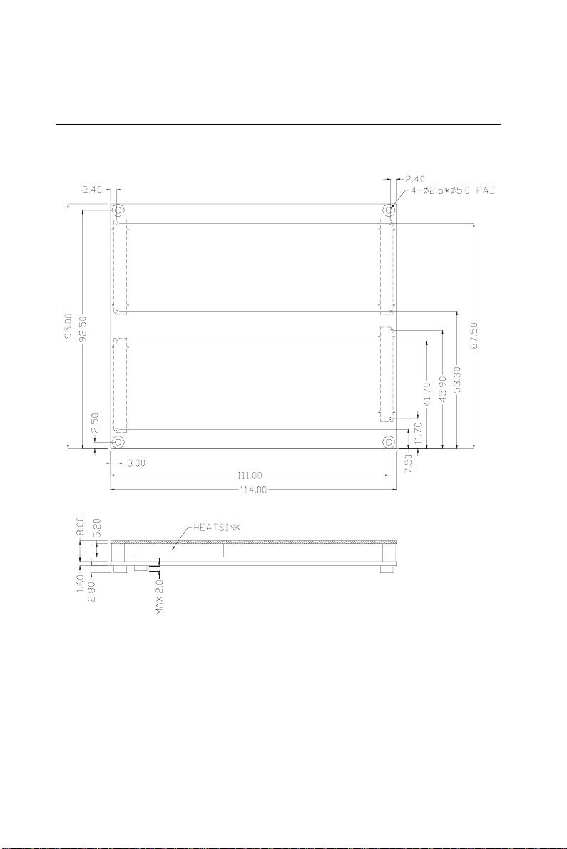
1.3 Board dimensions
Figure 1-1: SOM-4450 dimensions
6 SOM-4450 User's Manual
Page 13

Figure 1-2: SOM-4450 Top view
Chapter 1 General Information 7
Page 14

8 SOM-4450 User's Manual
Page 15

CHAPTER
2
Connector Assignments
and Descriptions
This chapter tells how to set up the SOM4450 hardware. It includes instructions on
connecting peripherals, switches and
indicators. Make sure you read all the
safety precautions before you begin the
installation procedure.
Page 16

2.1 Connector Locations
The board has a number of connectors that allow you to configure
your system to suit your application.
The tables below shows the function of each of the board's connectors:
SOM-4450 Locating Connectors
10 SOM-4450 User's Manual
Page 17

2. 2 Pin Assignments for X1, X2, X3, X4
connectors
Please refer to SOM-ETX Design and Specification Guide, Chapter 2
2.3 Safety precautions
Warning! Always completely disconnect the power cord from
your board whenever you are working on it. Do not
make connections while the power is on, because
sensitive electronic components can be damaged by
a sudden rush of power.
Caution! Always ground yourself to remove any static charge
before touching the board. Modern electronic devices
are very sensitive to static electric charges. Use a
grounding wrist strap at all times. Place all electronic
components on a static-dissipative surface or in a
static-shielded bag when they are not in the chassis.
Chapter 2 Connectors and Pin Assignments 11
Page 18

12 SOM-4450 User's Manual
Page 19

CHAPTER
3
Software Configuration
(optional for SOM-4450)
This chapter details the software configuration information. It shows you how to
configure the SOM-4450 card to match
your application requirements. Award
system BIOS is covered in Chapter 4.
Sections include:
• LCD display configuration
• Connections for two standard LCDs
Page 20

3.1 Introduction
The SOM-4450 system BIOS and custom drivers are located in a 256
KB, 32-pin Flash ROM device, designated U17. A single Flash chip
holds the system BIOS and VGA BIOS. The display type can be
configured via software. This method minimizes the number of chips
and eases configuration. You can change the display BIOS simply by
reprogramming the Flash chip.
3. 2 Utility CD disk
The SOM-4450 is supplied with a software utility on CD-ROM. This
disk contains the necessary file for setting up the VGA display.
Directories and files on the disk are as follows:
AWDFLASH.EXE
4450Vxxx.BIN
Figure 3-1: Contents of the SOM-4450 Series utility disk
A WDFLASH.EXE
This program allows you to update the BIOS Flash ROM.
4450110.BIN
This binary file contains the system BIOS.
3.3 VGA display software configuration
The SOM-4450 on-board VGA/LCD interface supports an 18-bit TFT
LCD, flat panel displays and traditional analog CRT monitors. The
interface can drive CRT displays with resolutions up to 1024 x 768 in 24
bpp. It is also capable of driving color panel displays with resolutions
of 1024 x 768 in 18 bpp. The LCD type is configured completely via the
software utility, so you do not have to set any jumpers. Configure the
LCD type as follows:
14 SOM-4450 User's Manual
Page 21

1 . Apply power to the SOM-4450 application with a color TFT display
attached. This is the default setting for the SOM-4450 series. Make
sure that the AWDFLASH.EXE and *.BIN files are located in the
working drive.
Note: Make sure that you do not run AWDFLASH.EXE
while your system is operating in EMM386 mode.
2. At the prompt, type AWDFLASH.EXE and press <Enter>. The
VGA configuration program will then display the following:
Figure 3-2: BIOS VGA setup screen
3 . At the prompt, type in the BIN file which supports your display.
When you are sure that you have entered the file name correctly
press <Enter>. The screen will ask “Do you want to save?” If you
wish to continue press Y. If you change your mind or have made a
mistake press N.
4 . If you decide to continue, the screen will issue a prompt which will
then ask “Are you sure to program (Y/N)?” If you wish to continue,
press Y. Press N to exit the program.
The new VGA configuration will then write to the ROM BIOS chip.
This configuration will remain the same until you run the
A WDFLASH.EXE program and change the settings.
Chapter 3 Software Configuration 15
Page 22

3.4 Connections for two standard LCDs
3.4.1 Connections for Toshiba LTM10C042(640 x 480
TFT color LCD)
Table 3-1: Connections for Toshiba LTM10C042
LTM10C042 SOM-4450
Pin Name Pin Name
1 GND 3 GND
2 CLK 35 SHFCLK
3 GND 4 GND
4 R0 27 PD12
5 R1 28 PD13
6 R2 29 PD14
7 GND 8 GND
8 R3 30 PD15
9 R4 31 PD16
10 R5 32 PD17
11 GND 33 GND
12 G0 19 PD6
13 G1 20 PD7
14 G2 21 PD8
15 GND 33 GND
16 G3 22 PD9
17 G4 23 PD10
18 G5 24 PD11
19 GND 34 GND
20 ENAB 37 M
21 GND 34 GND
22 B0 11 PD0
23 B1 12 PD 1
24 B2 13 PD 2
25 GND 39 GND
26 B3 14 PD 3
27 B4 15 PD 4
28 B5 16 PD 5
29 GND 39 GND
30 VDD 5 +5 V
31 VDD 6 +5 V
16 SOM-4450 User's Manual
Page 23

3.4.2 Connections for Toshiba LTM12C275A
(800 x 600 TFT color LCD)
Table 3-2: Connections for Toshiba LTM12C275A
LTM12C275A SOM-4450
Pin Name Pin Name
1 GND 3 GND
2 NCLK 35 SHFCLK
3NC - NC
4NC - NC
5 GND 4 GND
6 R0 27 PD12
7 R1 28 PD13
8 R2 29 PD14
9 R3 30 PD15
10 R4 31 PD16
11 R5 32 PD17
12 GND 8 GND
13 G0 19 PD6
14 G1 20 PD7
15 G2 21 PD8
16 G3 22 PD9
17 G4 23 PD10
18 G5 24 PD11
19 GND 33 GND
20 B0 11 PD0
21 B1 12 PD1
22 B2 13 PD2
23 B3 14 PD3
24 B4 15 PD4
25 B5 16 PD5
26 ENAB 37 M/DE
27 GND 34 GND
28 VCC 5 +5 V
29 VCC 6 +5 V
30 GND 39 GND
Chapter 3 Software Configuration 17
Page 24

18 SOM-4450 User's Manual
Page 25

APPENDIX
A
Programming the
Watchdog Timer
The SOM-4450 is equipped with a
watchdog timer that resets the CPU or
generates an interrupt if processing comes
to a standstill for any reason. This feature
ensures system reliability in industrial
standalone or unmanned
environments.
Page 26

A.1 Programming the watchdog timer
T o program the watchdog timer, you must write a program which writes
I/O port address 443 (hex). The output data is a value of time interval.
The value range is from 01 (hex) to 3E (hex), and the related time
interval is 1 sec. to 62 sec.
Data Time Interval
01 1 sec.
02 2 sec.
03 3 sec.
04 4 sec.
••
••
••
3E 62 sec.
20 SOM-4450 User's Manual
Page 27

After data entry , your program must refresh the watchdog timer by
rewriting the I/O port 443 (hex) while simultaneously setting it. When
you want to disable the watchdog timer, your program should read I/O
port 443 (hex).
The following example shows how you might program the watchdog
timer in BASIC:
1 0 REM W atchdog timer example program
2 0 OUT &H443, data REM Start and restart the watchdog
3 0 GOSUB 1000 REM Y our application task #1,
4 0 OUT &H443, data REM Reset the timer
5 0 GOSUB 2000 REM Y our application task #2,
6 0 OUT &H443, data REM Reset the timer
7 0 X=INP (&H443) REM, Disable the watchdog timer
80 END
1000 REM Subroutine #1, your application task
••
••
••
1070 RETURN
2000 REM Subroutine #2, your application task
••
••
••
2090 RETURN
Appendix A Programming the Watchdog Timer 21
Page 28

22 SOM-4450 User's Manual
Page 29

APPENDIX
B
System Assignments
• System I/O ports
• DMA channel assignments
• Interrupt assignments
• 1st MB memory map
Page 30

B.1 System I/O ports
Table B-1: System I/O ports
Addr. range
(Hex) Device
000-01F DMA controller (slave)
020-03F Interrupt controller 1, (master)
040-05F 8254 timer/counter
060-06F 8042 (keyboard controller)
070-07F Real-time clock, non-maskable interrupt (NMI)
mask
080-09F DMA page register,
0A0-0BF Interrupt controller 2 (slave)
0C0-0DF DMA controller (master)
0F0 Clear math co-processor
0F1 Reset math co-processor
0F8-0FF Math co-processor
170- 178 2nd fixed disk for CompactFlash
1F0-1F8 1st fixed disk
200-207 Game I/O
278-27F Reserved
2F8-2FF Serial port 2
300-31F Ethernet**
360-36F LPT2
378-37F Parallel printer port 1 (LPT1)
380-38F SDLC, bisynchronous 2
3A0-3AF Bisynchronous 1
3B0-3BF Monochrome display
3C0-3CF Reserved
3D0-3DF Color/graphics monitor adapter
3F0-3F7 Diskette controller
3F8-3FF Serial port 1
443 Watchdog timer
** default setting
24 SOM-4450 User's Manual
Page 31

B.2 DMA channel assignments
Table B-2: DMA channel assignments
Channel Function
0 Available
1 Available
2 Floppy disk (8-bit transfer)
3 Parallel**
4 Cascade for DMA controller 1
5 Available
6 Available
7 Available
** Parallel port DMA default setting: DMA 3
Parallel port DMA select: DMA 1, 3
Appendix B System Assignments 25
Page 32

B.3 Interrupt assignments
Table B-3: Interrupt assignments
Interrupt# Interrupt source
NMI Parity error detected
IRQ 0 Interval timer
IRQ 1 Keyboard
IRQ 2 Interrupt from controller 2 (cascade)
IRQ 3 Serial communication port 2
IRQ 4 Serial communication port 1
IRQ 5 Available
IRQ 6 Diskette controller (FDC)
IRQ 7 Parallel port 1 (print port)
IRQ 8 Real-time clock
IRQ 9 Reserve
IRQ 10 Available
IRQ 11 Reserved for watchdog timer
IRQ 12 PS/2 mouse
IRQ 13 INT from co-processor
IRQ 14 Preliminary IDE
IRQ 15 Secondary IDE for CompactFlash
USB and Ethernet IRQ is automatically set by the system
26 SOM-4450 User's Manual
Page 33

B.4 1st MB memory map
Table B-4: 1st MB memory map
Addr. range (Hex)Device
F000h - FFFFh System ROM
E000h - EFFFh Unused
CC00h - DFFFh available
C800h - CBFFh Ethernet ROM*
C000h - C7FFh VGA BIOS
B800h - BFFFh CGA/EGA/VGA text
B000h - B7FFh Reserved for graphic mode usage
A000h - AFFFh EGA/VGA graphics
0000h - 9FFFh Base memory
* default setting
Appendix B System Assignments 27
Page 34

28 SOM-4450 User's Manual
Page 35

APPENDIX
C
LVDS Connection
This appendix contains information
concerning the L VDS installation and pin
assignments.
Page 36

C.1 LVDS Introduction
When you mention the impressive data rate of 400 Mbps at 15 meters
for L VDS, you immediately realize how significant the differences are
between analog and digital interfaces. There are several other factors
other than significantly increased data transfer rate and image quality
that make L VDS (Low-Voltage Differential Signaling) very attractive to
industrial users. One is that L VDS drivers and receivers maintain
excellent signal levels and performance while operating on supply
voltages as low as 2 V. This low voltage allows LVDSs to operate
independently from the main power supply voltage. Another factor is
that L VDS drivers and receivers have a low swing voltage. This
voltage is typically around 345 mV. This allows LVDS devices to
achieve high speeds while using relatively little power. This low
differential swing voltage together with self-canceling EMI, reduces
EMI problems significantly. This is especially important in spacecritical applications. This is also why L VDS has already been widely
used in Notebook computer panel connections.
All Digital Benefits
No matter which digital standard an end user uses for their industrial
applications, it will have to provide the following criteria. Be compatible so that system and display products from different suppliers can
be made available in an open market. Become a standard for the
electronics and PC industry. Be able to transmit data over standard
twisted pair cables as well as fiber optic. Maintain a low bit error rate
for high quality image while operating at a very low power level. Be
scalable.
Expanded Applications
With flat panel displays already a common part of our everyday lives
at work, home and industrial/commercial settings, deciding on a
standard is a monumental decision that will affect all our lives.
Engineers will have to champion their cause by applying both of these
digital panel technologies to many practical products. Thus enabling
the end user, whether it be in an industrial setting or a consumer
setting, to benefit from both of these technologiesprocessor of choice.
30 SOM-4450 User's Manual
Page 37

C.2 LVDS Pin assingments
emaNniPlangisSDVLlennahC
0ODDCL-0tuoxTtsrif
1ODDCL+0tuoxTtsrif
2ODDCL-1tuoxTtsrif
3ODDCL+1tuoxTtsrif
4ODDCL-2tuoxTtsrif
5ODDCL+2tuoxTtsrif
6ODDCL-klcxTtsrif
7ODDCL+klcxTtsrif
8ODDCLdesuton-9ODDCLdesuton--
01ODDCLdesuton-11ODDCLdesuton-21ODDCLdesuton-31ODDCLdesuton-41ODDCLdesuton-51ODDCLdesuton-61ODDCLdesuton-71ODDCLdesuton-81ODDCLdesuton-91ODDCLdesuton--
Appendix C LVDS 31
Page 38

rebmuNniPlangiSrebmuNniPlangiS
1DNG2 DNG
3R4B
5YSH6 G
7YSV8 KCDD
9.C.N01ADDD
1161ODDCL2181ODDCL
3171ODDCL4191ODDCL
51DNG61DNG
7131ODDCL8151ODDCL
9121ODDCL0241ODDCL
12DNG22DNG
328ODDCL4211ODDCL
529ODDCL6201ODDCL
72DNG82DNG
924ODDCL037ODDCL
135ODDCL236ODDCL
33DNG43DNG
531ODDCL6330DDCL
730ODDCL832ODDCL
93CCV04CCV
142OIGTL240OIGTL
341OIGTL44#NOLB
54NOSAIB64NOGID
74PMOC84Y
94CNYS05C
15#YPLF/TPL25.C.N
35CCV45DNG
550VRD_BTS/65LESNED_DFA/
75RIF857DP
95XRRI06#LESDH_RRE/
16XTRI260TOM_6DP
362DXR46#RID_TINI/
56DNG66DNG
76#2STR865DP
96#2RTD07#PETS_NILS/
17#2DCD27#GHCKSD_4DP
37#2RSD47#ATADR_3DP
57#2STC67#PW_2DP
77#2DXT87#0KRT_1DP
97#2IR08#XEDNI_0DP
18CCV28CCV
381DXR481VRD_KCA/
58#1STR681TOM_YSUB/
78#1RTD88#ATADW_EP
98#1DCD09#ETAGW_TCLS/
19#1RSD29KLCSM
39#1STC49TADSM
591DXT69KLCBK
79#1IR89TADBK
99DNG001DNG
)draobyeK,esuoM,adrI,yppolF/TPL,2MOC,1MOC,oediV,DCL,AGV(3XrotcennoC
32 SOM-4450 User's Manual
 Loading...