

Page 1

AR-B1851 User’s Guide
AR-B1851
Pentium M inside,EPIC form factor ,On Board VGA,LVDS
with DDR SO-DIMM, built in Two LAN,CF Type-II
Edition: 1.1
Book Number: AR-B1851-2007/1/15
Page 2

AR-B1851 User’s Guide
@Copyright 2005
All Rights Reserved.
Manual first edition Nov 22, 2005
The information in this document is subject to change without prior
notice in order to improve reliability, design and function and does not
represent a commitment on the part of the manufacturer.
In no event will the manufacturer be liable for direct, indirect, special,
incidental, or consequential damages arising out of the use or inability to
use the product or documentation, even if advised of the possibility of
such damages.
This document contains proprietary information protected by copyright.
All rights are reserved. No part of this manual may be reproduced by
any mechanical, electronic, or other means in any form without prior
written permission of the manufacturer.
Trademarks
AR-B1851 is registered trademarks X-Fire Acrosser, IBM PC is a
registered trademark of International Business Machines Corporation.
Pentium is a registered trademark of Intel Technologies, Inc. Award is
registered trademarks of Award Software International, Inc. Other
product names mentioned herein are used for identification purposes
only and may be trademarks and/or registered trademarks of their
respective companies.
AR-B1851
2
Page 3

AR-B1851 User’s Guide
Contents
Contents................................................................ 3
Introduction............................................................. 5
1.1 Specifications:....................................................................... 5
1.2 What You Have..................................................................... 7
Installation .............................................................. 8
2.1 AR-B1851’s Layout............................................................... 8
2.2 Power Button Setting .......................................................... 10
2.3 CMOS Reset....................................................................... 11
2.4 Jumper description.............................................................. 11
Connection............................................................ 13
3.1 Ultra ATA33/66/100 IDE Disk Drive Connector(IDE1)....... 13
3.2 Serial Ports(COM1~4)........................................................ 14
3.3 Keyboard / Mouse Connector(MS_KB1) ............................ 15
3.4 USB Port Connector(USB1~4) ........................................... 15
3.5 Fan Connector (FAN1)........................................................ 16
3.6 LAN RJ45 Connector (LAN1/2)........................................... 16
3.7 Compact Flash Storage Card Socket(CF1)........................ 17
3.8 VGA Connector(VGA1)....................................................... 18
AR-B1851
3
Page 4

AR-B1851 User’s Guide
3.9 AUDIO Connector(AUDIO1)............................................... 18
3.10 DDR SODIMM Socket (J1)................................................. 19
3.11 8-BIT GPIO Connector(GPIO1).......................................... 19
3.12 Parallel port(PRN1)............................................................. 20
3.13 LVDS Connector(LVDS1) ................................................... 20
3.14 Speak Connector(SPK1).................................................... 19
Award BIOS Setup................................................ 21
4.1 Introduction ......................................................................... 21
4.2 Starting Setup ..................................................................... 21
4.3 Using Setup......................................................................... 21
4.4 Main Menu .......................................................................... 23
4.5 Advanced BIOS Features ................................................... 26
4.6 PnP/PCI Configuration Setup ............................................. 28
4.7 Peripheral............................................................................ 29
4.8 PC Health............................................................................ 31
4.9 Boot….. ...............................................................................32
4.10 Exit Selecting ...................................................................... 33
Appendix A. Watchdog Timer............................... 35
Appendix B: Digital I/O.......................................... 36
Appendix C: I/O Address Map.............................. 38
AR-B1851
4
Page 5

1
Introduction
1.1 Specifications:
CPU
: Supports Intel Pentium M, Celeron M CPU.
AR-B1851 User’s Guide
Chipset
RAM memory
Display Controller
Supports LVDS Encoders.
Ultra DMA 133 IDE Interface
CompactFlash
Compact Flash Disk or IBM Micro Drive.
Series ports
also support RS-422/485.
USB port :
Audio Connector:
Digital IO:
IrDA:
IR(ASKIR)interface.
PS/2 Mouse/Keyboard Connector
Watchdog timer
generate when CPU did not periodically trigger the timer.
Intel LAN Controller
Intel BCM4401(Optional) 10/100BASE-TX or BMC5788 1000BASE-TX
Connected to your LAN through RJ45 connector.
: GMCH 852GM and ICH4 82801DB
: DDR SDRAM SO-DIMM Socket support to 1GB/266MHz.
: Intel 852GM Supports non-interlaced CRT monitors
: One PCI Enhance IDE channel.
TM
interface
: Two high-speed 16C550 compatible UARTs ports.COM1 can
Support Four USB 2.0 compatible ports.
supports Line-in, Line-out, MIC-in.
Supports eight digital-in, and eight digital-out TTL-level I/O ports.
Supports Serial Infrared(SIR) or Amplitude Shift Keyed
: Time setting form 1 to 255 second / minute System Reset
: Supports CompactFlash
:
Two ports IEEE 802.3u Auto-Negotiation support for
TM
Type II socket for
.
AR-B1851
5
Page 6

AR-B1851 User’s Guide
Power Consumption
Operating Temperature
Dimension:
146mm(W) X 101.6mm(L)
: 12V / 5V
: -10° ~ 60° C ( CPU needs Cooler)
AR-B1851
6
Page 7

AR-B1851 User’s Guide
1.2 What You Have
In addition to this User's Manual, the AR-B1851 package includes the
following items:
AR-B1851 board
User Manual
Drive CD
AR-B1851
7
Page 8
AR-B1851 User’s Guide
2
Installation
This chapter describes how to install the AR-B1851. At first, the
layout of AR-B1851 is shown, and the unpacking information that you
should be careful is described. The jumpers and switches setting for
the AR-B1851’s configuration
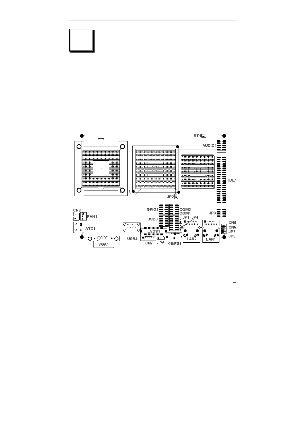
2.1 AR-B1851’s Layout
Top Placement
AR-B1851
8
Page 9
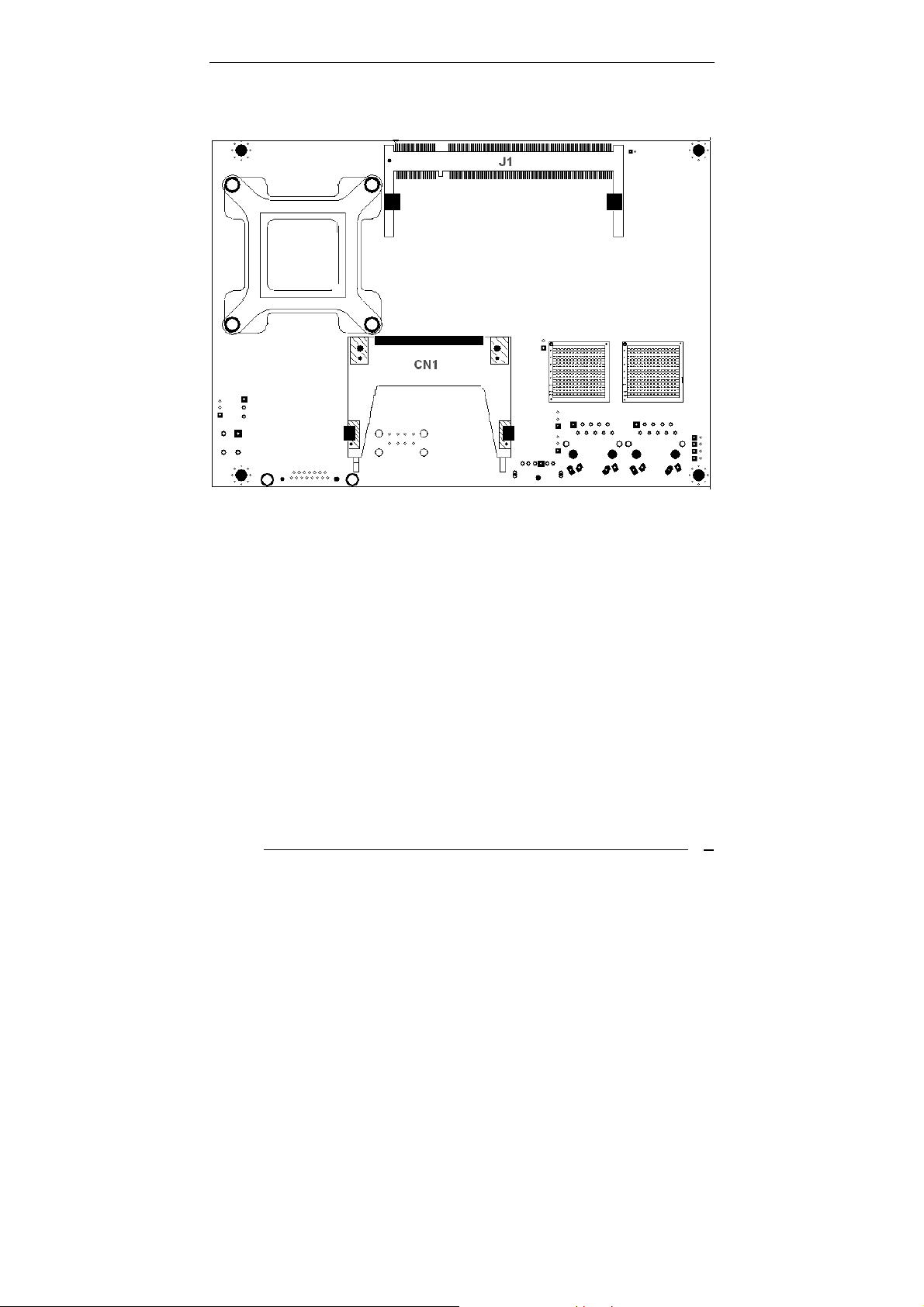
AR-B1851 User’s Guide
Bottom Placement
AR-B1851
9
Page 10
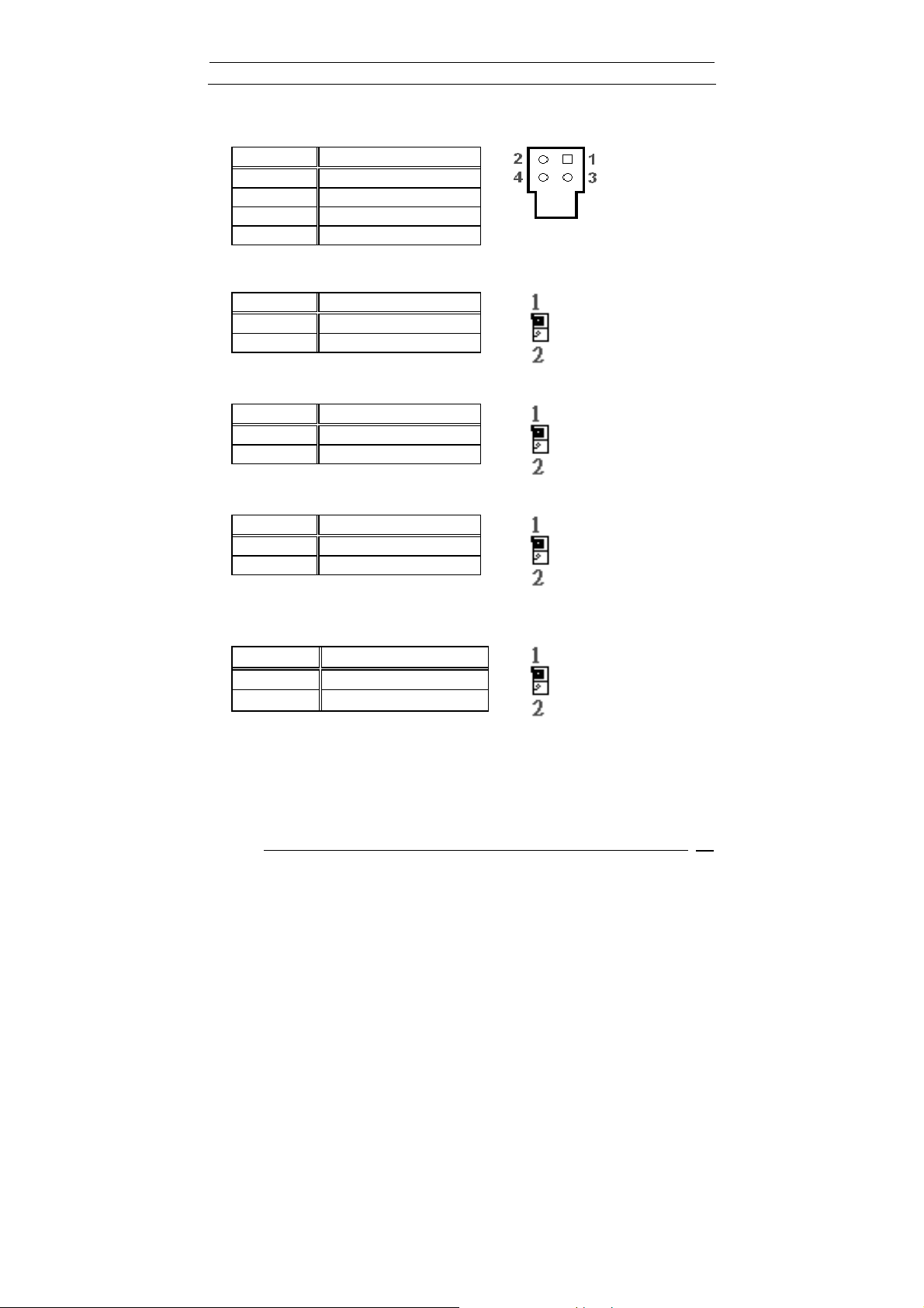
2.2 Power Button Setting
ATX1 : Power Connector
•
Pin DESCRIPTION
1 +12V
2 GND
3 +5V
4 GND
Connector
Pin DESCRIPTION
1 +5VSB
2 Power ON
JP7 : Power LED
•
Pin DESCRIPTION
1 +5V
2 GND
JP8 : HDD LED
•
Pin DESCRIPTION
1 +5V
2 GND
CN6 : Reset Button Connector
•
Pin DESCRIPTION
Open Normal
Short Reset System
AR-B1851 User’s Guide
CN5 : Power Button
•
AR-B1851
10
Page 11
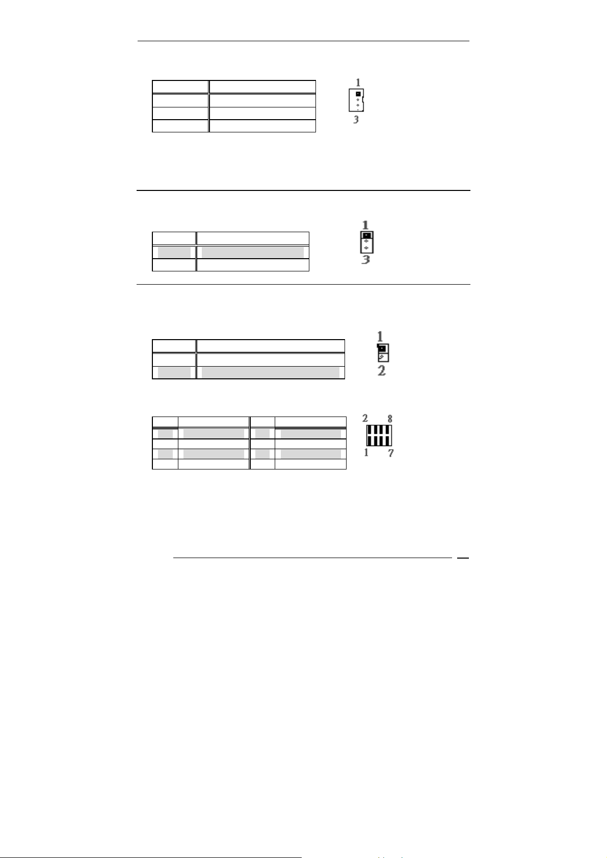
CN8 : Power ON Pin Header
•
Pin DESCRIPTION
1 GND
2 PS_ON
3 5VSB
2.3 CMOS Reset
JP1 : CMOS pin header
•
JP1 DESCRIPTION
1-2 Normal Operation
2-3 Clear CMOS
2.4 Jumper description
JP2 : Select CF Master or Slave mode
•
AR-B1851 User’s Guide
JP2 Description
Short Master
Open Slave
• JP3 : COM1/2 Select RI is 12V or signal
PIN DESCRIPTION PIN DESCRIPTION
1 NRIA 2 NRIA_12V
3 +12V 4 NRIA_12V
5 NRIB 6 NRIB_12V
7 +12V 8 NRIB_12V
AR-B1851
11
Page 12

JP4 : Select COM4 is RS232 or RS422/485
•
JP4 Description
1-2 RS232
2-3 RS422/485
JP6 : Select LCD Voltage
•
JP6 Description
1-2 +3.3V
2-3 +5V
AR-B1851 User’s Guide
AR-B1851
12
Page 13
AR-B1851 User’s Guide
3
Connection
This chapter describes how to connect peripherals, switches and
indicators to the AR-B1851 board.
3.1 Ultra ATA33/66/100 IDE Disk Drive Connector(IDE1)
You can attach two IDE( Integrated Device Electronics) hard disk drives
to the AR-B1851 IDE controller.
IDE 1 : Secondary IDE Connector (44 Pins)
PIN NO. DESCRIPTION PIN NO. DESCRIPTION
1 RESET# 2 GROUND
3 DATA 7 4 DATA 8
5 DATA 6 6 DATA 9
7 DATA 5 8 DATA 10
9 DATA 4 10 DATA 11
11 DATA 3 12 DATA 12
13 DATA 2 14 DATA 13
15 DATA 1 16 DATA 14
17 DATA 0 18 DATA 15
19 GROUND 20 N/C
21 N/C 22 GROUND
23 IOW# 24 GROUND
25 IOR# 26 GROUND
27 N/C 28 BALE - DEFAULT
29 N/C 30 GROUND - DEFAULT
31 INTERRUPT 32 IOCS16#-DEFAULT
33 SA1 34 N/C
35 SA0 36 SA2
37 HDC CS0# 38 HDC CS1#
39 HDD ACTIVE# 40 GROUND
41 +5V LOGIC 42 +5V MOTOR
43 GROUND 44 TYPE
12
43
44
AR-B1851
13
Page 14

AR-B1851 User’s Guide
3.2 Serial Ports(COM1~4)
The AR-B1851 offers two high speeds NS16C550 compatible UARTs
with Read/Receive 16 byte FIFO serial ports.
• COM2 : RS-232 Serial port (Pin Header)
PIN DESCRIPTION PIN DESCRIPTION
1 -DCD 2 -DSR
3 RXD 4 -RTS
5 TXD 6 -CTS
7 -DTR 8 -RI
9 GND 10 NC
COM1 : RS-232 with RS-422/485 Serial port(Pin Header)
•
PIN DESCRIPTION PIN DESCRIPTION
1 -DCD 2 -DSR
3 RXD 4 -RTS
5 TXD 6 -CTS
7 -DTR 8 -RI
9 GND 10 GND
11 TX+ 12 TX13 RX+ 14 RX-
AR-B1851
14
Page 15

AR-B1851 User’s Guide
3.3 Keyboard / Mouse Connector(MS_KB1)
A PS/2 type connector(MS_KB1)is for easy connection to a keyboard
and PS/2 mouse. The board comes with a Y split PS/2 cable for
keyboard and mouse connection.
KB/MS1 : Keyboard Mouse PS2 Port
•
PIN DESCRIPTION PIN DESCRIPTION
1 KB_DAT 2 MS_DAT
3 GND 4 X
5 +5V 6 KB_CLK
7 X 8 MS_CLK
3.4 USB Port Connector(USB1~4)
The AR-B1851 provides four USB port, four pin header, two connectors .
USB4 : USB Connector
•
PIN DESCRIPTION PIN DESCRIPTION
1
3
5
7
9
VCC
USB-
USB+
GND
USB_GND
2
4
6
8
10
VCC
USB-
USB+
GND
USB_GND
• USB3 : USB Connector(Pin header)
PIN DESCRIPTION PIN DESCRIPTION
1
3
5
7
9
VCC
USB0-
USB0+
GND
USB_GND
2
4
6
8
10
VCC
USB1-
USB1+
GND
USB_GND
AR-B1851
15
Page 16

AR-B1851 User’s Guide
3.5 Fan Connector (FAN1)
The AR-B1851 provides one connectors for CPU cooling fan they can be
controlled by Super I/O Chip.
FAN1: Fan Connector for CPU
•
PIN NO. DESCRIPTION
1 GND
2 +12V
3 PWM Signal
3.6 LAN RJ45 Connector (LAN1/2)
AR-B1851 is equipped with built-in 10/100Mbps(Option) or
1000MbpsEthernet Controller. You can connect it to your LAN through
RJ45 LAN connector. The pin assignments are as following:
• LAN1/2 : LAN RJ45 Connector
PIN NO. DESCRIPTION PIN NO. DESCRIPTION
1 TX+ 5. N/C
2 TX- 6. RX-
3. RX+ 7. N/C
4. N/C 8. N/C
81
AR-B1851
16
Page 17

AR-B1851 User’s Guide
3.7 Compact Flash Storage Card Socket(CF1)
The AR-B1851 configures Compact Flash Storage Card in IDE Mode.
This type II Socket is compatible with IBM Micro Drive.
CF1 : Compact Flash Storage Card Socket pin assignment
•
PIN NO. DESCRIPTION PIN NO. DESCRIPTION
1 GROUND 26 CARD DETECT1
2 D3 27 D11
3 D4 28 D12
4 D5 29 D13
5 D6 30 D14
6 D7 31 D15
7 CS1# 32 CS3#
8 N/C 33 N/C
9 GROUND 34 IOR#
10 N/C 35 IOW#
11 N/C 36 PULL HIGH
12 N/C 37 IRQ15
13 VCC 38 VCC
14 N/C 39 MASTER/SLAVE
15 N/C 40 N/C
16 N/C 41 RESET#
17 N/C 42 IORDY
18 A2 43 N/C
19 A1 44 PULL HIGH
20 A0 45 ACTIVE#
21 D0 46 PDIAG#
22 D1 47 D8
23 D2 48 D9
24 N/C 49 D10
25 CARD DETECT2 50 GROUND
Note: If IDE2 & CFD1 both in used, CFD1 must be as “Master” & IDE2 is as “Slave”.
AR-B1851
17
Page 18

AR-B1851 User’s Guide
3.8 VGA Connector(VGA1)
The AR-B1851 has a built-in 15-pin VGA connector accepting the CRT
monitor
VGA1 : 15-pin D-Sub Connector
•
PIN DESCRIPTION PIN DESCRIPTION
1 L_RED 2 L_GREEN
3 L_BLUE 4 MON2PU
5 GND 6 GND
7 GND 8 GND
9 +5V 10 GND
11 MONOPU 12 5VDDCDA
13 HSYNC 14 VSYNC
15 5VDDCCL
NOTE:
When system boots up without the MONITOR attached during the POST, the
VBIOS will disable the MONITOR output. Under this condition, the MONITOR
display will not work and the system will need to be rebooted with the
MONITOR attached to enable the display. The problem originates from the
VBIOS of the IntelR Extreme Graphics Driver, which disables the MONITOR
output if a MONITOR is not detected during POST.
3.9 AUDIO Connector(AUDIO1)
AUDIO1 : Audio Pin Header
•
PIN DESCRIPTION PIN DESCRIPTION
1 LINE_OUT_R 2 LINE_OUT_L
3 GND 4 GND
5 LINE_IN_R 6 LINE_IN_L
7 MIC_IN 8 GND
9 GND 10 GND
AR-B1851
18
Page 19

AR-B1851 User’s Guide
3.10 DDR SODIMM Socket (J1)
There are two 200-pin DDR SDRAM DIMM slots to accept 2.5V non_buffered
DDR SDRAM. The max Memory size is 2GB.
• J1 : DDR SODIMM Socket
3.11 8-BIT
GPIO Connector(GPIO1)
• GPIO1: 8 BIT GPIO Connector
PIN DESCRIPTION PIN DESCRIPTION
1 GP10 2 GP11
3 GP12 4 GP13
5 GP14 6 GP15
7 GP16 8 GP17
9 GND 10 VCC
3.14 Speak Connector(SPK1)
• SPK1 : Speak out Connector(through Amplifier)
PIN NO. DESCRIPTION
1 SPKR
2 GND
3 SPKL
4 GND
AR-B1851
19
Page 20

AR-B1851 User’s Guide
3.12 Parallel port(PRN1)
This port is usually connected to a printer. The AR-B1851 includes an on-board
parallel port.
• PRN1: Parallel Port Connector
PIN DESCRIPTION PIN DESCRIPTION
1 STB- 14 AFD-
2 PD0 15 ERR-
3 PD1 16 INIT-
4 PD2 17 SLIN-
5 PD3 18 GND
6 PD4 19 GND
7 PD5 20 GND
8 PD6 21 GND
9 PD7 22 GND
10 ACK- 23 GND
11 BUSY 24 GND
12 PE 25 GND
13 SLCT 26 X
3.13 LVDS Connector(LVDS1)
• LVDS1 : LVDS Interface Connector
PIN DESCRIPTION PIN DESCRIPTION
2 GND 1 LVDS_PWR
4 LVDS_CLKBP 3 LVDS_CLKBM
6 LVDS_YBM2 5 GND
8 GND 7 LVDS_YBP2
10 LVDS_YBP1 9 LVDS_YBM1
12 LVDS_YBM3 11 LVDS_YBP3
14 LVDS_YBM0 13 LVDS_YBP0
16 LVDS_CLKAP 15 GND
18 GND 17 LVDS_CLKAM
20 LVDS_YAM2 19 LVDS_YAP2
22 LVDS_YAP1 21 DDCPCLK_X
24 DDCPDATA_X 23 LVDS_YAM1
26 LVDS_YAM0 25 LVDS_YAP0
28 LVDS_YAM3 27 LVDS_YAP3
30 LVDS_PWR 29 LVDS_PWR
AR-B1851
20
Page 21

AR-B1851 User’s Guide
4
Award BIOS Setup
4.1 Introduction
This chapter discusses the Setup program built into the BIOS. The
Setup program allows users to configure the system. This configuration
is then stored in battery-backed CMOS RAM so that it retains the Setup
information while the power is off.
4.2 Starting Setup
The BIOS is immediately active when you turn on the computer. While
the BIOS is in control, the Setup program can be activated in one of two
ways:
1. By pressing <Del> immediately after switching the system on, or
2. By pressing the <Del> key when the following message appears
briefly at the bottom of the screen during the POST (Power On SelfTest).
Press DEL to enter SETUP.
If the message disappears before you respond and you still wish to enter
Setup, restart the system to try again by turning it OFF then ON or
pressing the "RESET" button on the system case. You may also restart
by simultaneously pressing <Ctrl>, <Alt>, and <Delete> keys. If you do
not press the keys at the correct time and the system does not boot, an
error message will be displayed and you will again be asked to...
PRESS F1 TO CONTINUE, DEL TO ENTER SETUP
4.3 Using Setup
AR-B1851
21
Page 22

AR-B1851 User’s Guide
In general, you can use the arrow keys to highlight items, press <Enter>
to select, use the PageUp and PageDown keys to change entries, press
<F1> for help and press <Esc> to quit. The following table provides
more details about how to navigate in the Setup program using the
keyboard.
Key Function
Up Arrow Move to the previous item
Down
Arrow
Left Arrow Move to the item on the left (menu bar)
Right Arrow Move to the item on the right (menu bar)
Esc Main Menu: Quit without saving changes
Move Enter Move to the item you desired
PgUp key Increase the numeric value or make changes
PgDn key Decrease the numeric value or make changes
+ key Increase the numeric value or make changes
- key Decrease the numeric value or make changes
Esc key Exit Menu -- Quit and not save changes into CMOS
F1 key General help on Setup navigation keys
F5 key Load previous values from CMOS
F6 key Load the fail-safe defaults from BIOS default table
F7 key Load the optimized defaults
F10 key Save all the CMOS changes and exit
Move to the next item
Submenus: Exit Current page to the next higher level
menu
Status Page Setup Menu and Option Page Setup
Menu -- Exit current page and return to Main Menu
AR-B1851
22
Page 23

AR-B1851 User’s Guide
4.4 Main Menu
The items in Standard CMOS Setup Menu are divided into 10 categories.
Each category includes no, one or more than one setup items. Use the
arrow keys to highlight the item and then use the <PgUp> or <PgDn>
keys to select the value you want in each item.
Figure 1: The Main Menu
Main Menu Selections
Item Options Description
Date MM DD YYYY Set the system date.
Time HH : MM : SS Set the system time
IDE
Primary Master
IDE
Primary Slave
IDE
Secondary Master
IDE Options are in its sub Press <Enter> to enter
Options are in its sub
menu
(described in Table 3)
Options are in its sub
menu
(described in Table 3)
Options are in its sub
menu
(described in Table 3)
AR-B1851
Press <Enter> to enter
the sub menu of detailed
options
Press <Enter> to enter
the sub menu of detailed
options
Press <Enter> to enter
the sub menu of detailed
options
23
Page 24

AR-B1851 User’s Guide
Secondary Slave menu
(described in Table 3)
Drive A & Drive B None
360K, 5.25 in
1.2M, 5.25 in
1.720K, 3.5 in
1.44K, 3.5 in
2.88K, 3.5 in
Video EGA / VGA
CGA 40
CGA 80
Mono
Halt On All Errors
No Errors
All, but Keyboard
All, but Diskette
All, but Disk/Key
Base Memory N/A Displays the amount of
Extended Memory N/A Displays the amount of
Total Memory N/A Displays the total
Table 1 Main Menu Selections
the sub menu of detailed
options
Select what kind of floppy
type you install
Select what type of
Display you use
Select the situation in
which you want the BIOS
to stop the POST
process and notify you
conventional memory
detected during boot up
extended memory
detected during boot up
memory available in the
system
IDE Adapters
The IDE adapters control the hard disk drive. Use a separate sub menu
to configure each hard disk drive.
Figure 2 shows the IDE primary master sub menu.
IDE HDD Auto-Detection [Press Enter]
IDE Primary Master [Auto]
Access Mode [Auto]
C a p a c i t y 0 M B
AR-B1851
24
Page 25

AR-B1851 User’s Guide
Cylinder 0
H e a d 0
P r e c o m p 0
Landing Zone 0
S e c t o r 0
Figure 2 IDE Primary Master sub menu
Use the legend keys to navigate through this menu and exit to
the main menu. Use Table 2 to configure the hard disk.
Item Options Description
IDE HDD Auto-detection Press Enter Press Enter to auto-detect
the HDD on this channel. If
detection is successful, it fills
the remaining fields on this
menu.
IDE Primary Master None
Auto
Manual
Capacity Auto Display
your disk drive
size
Access Mode CHS
LBA
Large
Auto
Table 2 Hard disk selections
Selecting ‘manual’ lets you
set the remaining fields on
this screen. Selects the type
of fixed disk. "User Type"
will let you select the number
of cylinders, heads, etc.
Note: PRECOMP=65535
means NONE !
Disk drive capacity
(Approximated). Note that
this size is usually slightly
greater than the size of a
formatted disk given by a
disk checking program.
Choose the access mode for
this hard disk
AR-B1851
25
Page 26

AR-B1851 User’s Guide
4.5 Advanced BIOS Features
This section allows you to configure your system for basic operation.
Figure 3 Advanced menu
APIC Mode
This item allows use Advanced Programmable Interrupt Controller feature.The
Choice: Enabled, Disabled.
Quick Power On Self Test
This category speeds up Power On Self Test (POST) after you power up
the computer. If it is set to Enable, BIOS will shorten or skip some check
items during POST.
Enabled Enable quick POST
Disabled Normal POST
Full Screen LOGO Show
This item allows you to enable or disable show full screen LOGO
.
The Choice: Enabled, Disabled.
USB Keyboard Support
This item allows you to enable or disable USB keyboard support.
The Choice: Enabled, Disabled.
AR-B1851
26
Page 27

AR-B1851 User’s Guide
PS/2 Mouse Function
Disabled-prevents any installed PS/2 mouse from functioning but frees
up IRQ12.Enabled-allows the operating system to determine whether to
enable or disable the mouse. Choice: Enabled, Disabled.
Init Display First
This item allows you to choose which Display to be first detected.
The Choice: PCI Slot, On Board / AGP.
Intel VGA Share Memory
This item allows you to Choose the Frame Buffer size for Display.
The Choice: 1MB, 4MB, 8MB, 16MB, 32MB.
Boot Display
This item allows you to choose display interface
.
The Choice: Vbios default, CRT, EFP, TV, CRT + EFP, CRT + TV.
Panel Type
This item allows you to choose display panel type and resolution
.
The Choice: 640x480,800x600,1024x768.
ACPI Function
This item allows you to enable or disable
Power Management (
The Choice: Enabled, Disabled.
ACPI) function.
Advanced Configuration and
ACPI Suspend Type
This item allows you to Choose Suspend Type for ACPI function.
The Choice: S1(Pos), S3(STR), S1 & S3.
Power Supply Type
This item allows you to choose the Type of Power Supply in use.
The Choice: AT, ATX.
PWRON After Power-Fail
This item allows you to choose the Option of Power Status after Power
Fail by ATX Power Supply.
The Choice: Former-STS, On, Off.
AR-B1851
27
Page 28

AR-B1851 User’s Guide
4.6 PnP/PCI Configuration Setup
Figure 4 PnP/PCI menu
Resource controlled by
The Award Plug and Play BIOS has the capacity to automatically
configure all of the boot and Plug and Play compatible devices. However,
this capability means absolutely nothing unless you are using a Plug and
Play operating system such as Windows®95. If you set this field to
“manual” choose specific resources by going into each of the sub menu
that follows this field (a sub menu is preceded by a “”).
The choice: Auto(ESCD), Manual.
IRQ Resources
When resources are controlled manually, assign each system interrupt a
type, depending on the type of device using the interrupt.
IRQ3/4/5/7/9/10/11/12/14/15 assigned to
This item allows you to determine the IRQ assigned to the ISA bus and is
not available to any PCI slot. Legacy ISA for devices compliant with the
original PC AT bus specification, PCI/ISA PnP for devices compliant with
the Plug and Play standard whether designed for PCI or ISA bus
architecture.
The Choice: PCI Device, Reserved.
AR-B1851
28
Page 29

AR-B1851 User’s Guide
4.7 Peripheral
Figure 5 Peripheral menu
Onboard Serial Port 1/Port 2
Select an address and corresponding interrupt for the first and second
serial ports.
The choice: 3F8/IRQ4, 2E8/IRQ3, 3E8/IRQ4, 2F8/IRQ3, Disabled,
Auto
UART Mode Select
Select the Function Mode for UART.
The choice: IrDA, ASKIR, Normal
Onboard Serial Port 3/Port 4
Select an address and corresponding interrupt for the first and second
serial ports.
The choice: 3F8/IRQ4, 2E8/IRQ3, 3E8/IRQ4, 2F8/IRQ3, Disabled,
Auto
AR-B1851
29
Page 30

AR-B1851 User’s Guide
Onboard Parallel Port
Select 3BC/IRQ7 to enable On Board Parallel Port as first Parallel
Interface.
The choice: Disable, 378/IRQ7, 278/IRQ5, 3BC/IRQ7.
USB Controller
Select Enabled if your system contains a Universal Serial Bus (USB)
controller and you have USB peripherals.
The Choice: Enabled, Disabled.
USB 2.0 Controller
This Entry is for disable / enable EHCI controller only. The Bios itself may
/ may not have high speed USB support. If the Bios has high speed USB
support built in, the support will be automatically turn on when high
speed device were attached.
The Choice: Enabled, Disabled.
AC97 AUDIO
The Choice: Auto, Disabled.
AR-B1851
30
Page 31

AR-B1851 User’s Guide
4.8 PC Health
Figure 5 H/W Monitor menu
Shutdown Temperature
This item allows the system to reset when temperature reach the trigger
level.
The Choice: Disabled, 60°C/140°F, 65°C/149°F, 70°C/158°F, 75°C/167
°F
AR-B1851
31
Page 32

4.9 Boot
AR-B1851 User’s Guide
Figure 6 Boot menu
First/Second/Third/Other Boot Device
The BIOS attempts to load the operating system from the devices in the
sequence selected in these items.
The Choice:
Floppy ………. [ ]
LS120 ………. [ ]
Hard Disk …. [ ]
CDROM … …….[ ]
ZIP100 ………. [ ]
USB-FDD .. …...[ ]
USB-ZIP .. …...[ ]
USB-CDROM .. [
▪]
On Board LAN …[ ]
Disabled ….. ……[ ]
AR-B1851
32
Page 33

4.10 Exit Selecting
Save & Exit Setup
Load Optimized Defaults
Exit Without Saving
Load Fail-Save Default
AR-B1851 User’s Guide
Figure 8
Save & Exit Setup
Pressing <Enter> on this item asks for confirmation:
Save to CMOS and EXIT (Y/N)? Y
Pressing “Y” stores the selections made in the menus in CMOS – a
special section of memory that stays on after you turn your system off.
The next time you boot your computer, the BIOS configures your system
according to the Setup selections stored in CMOS. After saving the
values the system is restarted again.
Load Optimized Defaults
Exit menu
AR-B1851
33
Page 34

AR-B1851 User’s Guide
Use this menu to load the BIOS default values that are factory
settings for optimal performance system operations. While Award
has designed the custom BIOS to maximize performance, the
factory has the right to change these defaults to meet their needs.
When you press <Enter> on this item you get a confirmation dialog box
with a message similar to:
Load Optimized Defaults (Y/N) ? N
Pressing ‘Y’ loads the default values that are factory settings for optimal
performance system operations.
Exit Without Saving
Pressing <Enter> on this item asks for confirmation:
Quit without saving (Y/N)? Y
This allows you to exit Setup without storing in CMOS any change. The previous
selections remain in effect. This exits the Setup utility and restarts your computer.
Load Fail-Safe Defaults
Use this menu to load the BIOS default values that are factory
settings for safety system operations.
When you press <Enter> on this item you get a confirmation dialog box
with a message similar to:
Load Fail-Safe Defaults (Y/N) ? N
Pressing ‘Y’ loads the default values that are factory settings for
Fail-Safe system operations.
AR-B1851
34
Page 35

AR-B1851 User’s Guide
Appendix A. Watchdog Timer
The WDT(Watch Dog Timer)is used to generate a variety of
output signals after a user programmable cont. The WDT is
suitable for use in the prevention of system lock-up, such as
when software becomes trapped in a deadlock. Under these
sort of circumstances, the timer will count to zero and the
selected outputs will be driven. Under normal circumstance,
the user will restart the WDT at regular intervals before the
timer counts to zero.
WATCHDOG TIMER SETTING
The watchdog timer is a circuit that maybe be used from your
program software to detect crash or hang up. The watchdog
timer is automatically disabled after reset. Once you enabled
the watchdog timer, your program should trigger the watchdog
timer every time before it times out. After you trigger the
watchdogtimer, the timer will be set to zero and start to count
again. If your program fails to trigger the watchdog timer
before times out, it will generate a reset pulse to reset the
system or trigger the IRQ9 signal in order to tell your system
that the watchdog time is out.
User could test watch dog function under ’Debug.exe’ program
as follows:
WDT Example
o 2e 87 ;Extended Functions Enable Register
o 2e 87 ;Extended Functions Enable Register
o 2e 07 ;EFIR=EFER(Extended Function Index
o 2f 08 ;EFDR=EFIR+1, select logical device 8
o 2e 30 ;select CR30
o 2f 01 ;update CR30 with value 01H
o 2e f6 ;select CRF6
o 2f 08 ;update CRF6 with value 08H,(8sec reset)
g ;go
Description
Register)point to Logical Device Number Reg.
AR-B1851
35
Page 36

AR-B1851 User’s Guide
Appendix B: Digital I/O
One characteristic of digital circuit is its fast response to high or
low signal. This kind of response is highly needed for harsh and
critical industrial operating environment. Digital Input and
Output, generally, are control signals. You can use these
signals to control external devices that needs On/Off circuit or
TTL devices. You can read or write data to the selected address
to enable the function of digital IO.
Users could test GPIO function under ‘Debug.exe’ program as
follow:
GPO Example Description
O 2E 87 ;Eetended Functions Enable Register
O 2E 87 ;Eetended Functions Enable Register
O 2E 2A ;Select CR2A
O 2F FC ;(Define the PINs as GPIO or Game Port 1)
“FC” Pin 121~128 set as GPIO
O 2E 07 ;EFIR=EFER(Extended Functions Index
Register)point to Logical Device Number Reg.
O 2F 07 ;EFDR=EFIR+1(select logical device 7,GPIO in
logical device 7)
O 2E 30 ;select CR30(Active or inactive)
O 2F 01 ;set 01(Active), 00(inactive)
O 2E F0 ;select CRF0(Set the PINs be GPO or GPI
Function)
O 2F 00 ;set the PINs be GPO
O 2E F2 ;select CRF2(Output High/Low)
O 2F 00 ;set the PINs be all Low Level(FF=all High
Level)
O 2E F1 ;select CRF1
O 2F FF ;set the Output to be FF(all High)
O 2E AA ;exit EFER
Q ;quit debug
AR-B1851
36
Page 37

AR-B1851 User’s Guide
GPI Example Description
O 2E 87 ;Extended Functions Enable Register
O 2E 87 ;Extended Functions Enable Register
O 2E 2A ;select CR2A
O 2F FC ;(Define the PINs as GPIO or Game
Port1)”FC”Pin121~128 set as GPIO
O 2E 07 ;EFIR=EFER(Extended Functions Index
Register)point to Logical Device Number Reg.
O 2F 07 ;EFDR=EFIR+1(select logical device 7,GPIO in
logical device7)
O 2E 30 ;select CR30(Active or inactive)
O 2F 01 ;set 01(Active) , 00(Inactive)
O 2E F0 ;select CRF0(Set the PINs be GPO or GPI
Funciton)
O 2F FF ;set the PINs be GPI
O 2E F1 ;select CRF1(Set the PINs be Read only)
I 2F ;Show the PINs Value
Q ;Quit debug
AR-B1851
37
Page 38

AR-B1851 User’s Guide
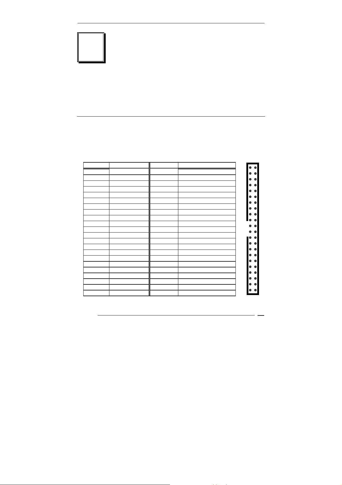
Appendix C: I/O Address Map
I/O ADDRESS MAP
I/O ADDRESS MAP DESCRIPTION
00000000-0000000F DMA Controller
00000000-00000CF7 PCI Bus
00000010-0000001F Mainboard Resource
00000020-00000021
00000022-0000003F Mainboard Resource
00000040-00000043 System Timer
00000044-0000005F Mainboard Resource
00000060-00000060 Standard 101/102 keyboard Controller
00000061-00000061 System Speaker
00000062-00000063 Mainboard Resource
00000064-00000064 Standard 101/102 keyboard Controller
00000065-0000006F Mainboard Resource
00000070-00000073 System CMOS/RTC
00000074-0000007F Mainboard Resource
00000080-00000090 DMA Controller
00000091-00000093 Mainboard Resource
00000094-0000009F DMA Controller
000000A0-000000A1 Programable interrupt controller
000000A2-000000BF Mainboard Resource
000000C0-000000DF DMA Controller
000000E0-000000EF Mainboard Resource
000000F0-000000FF Math Coprocessor
00000170-00000177 Secondary IDE Channel
000001F0-000001F7 Primary IDE Channel
00000274-00000277 ISAPNP Read Data Port
00000279-00000279 ISAPNP Read Data Port
00000294-00000297 Mainboard Resource
000002E8-000002EF COM4
000002F8-000002FF COM2
00000376-00000376 Secondray IDE Channel
00000378-0000037F LPT
Programable Interrupt Controller
AR-B1851
38
Page 39

AR-B1851 User’s Guide
000003B0-000003BB Graphics Controller
000003C0-000003DF Graphics Controller
000003E8-000003EF COM3
000003F6-000003F6 Primary IDE Channel
000003F8-000003FF COM1
00000400-000004BF Mainboard Resource
000004D0-000004D1 Mainboard Resource
00000500-0000051F SMBus
00000778-0000077B LPT
00000A78-00000A7B Mainboard Resource
00000B78-00000B7B Mainboard Resource
00000BBC-00000BBF Mainboard Resource
00000D00-0000FFFF PCI Bus
00000E78-00000E7B Mainboard Resource
00000F78-00000F7B Mainboard Resource
00000FBC-00000FBF Mainboard Resource
0000D000-0000D03F 100M Network Connection
0000D100-0000D13F 100M Network Connection #2
0000E000-0000E0FF AC’97 Audio
0000E800-0000E81F USB Universal Host Controller
0000E900-0000E907 Graphics Controller
0000EB00-0000EB1F USB Universal Host Controller
0000EC00-0000EC3F AC’97 Audio
0000ED00-0000ED1F USB Universal Host Controller
0000F000-0000F00F Ultra ATA Storage Controller
1ST MB MEMORY ADDRESS MAP
MEMORY ADDRESS DESCRIPTION
00000000-0009FFFF System Mainboard
000A0000-000BFFFF Graphics Controller
000A0000-000BFFFF PCI Bus
000C0000-000DFFFF PCI Bus
000CCA00-000CFFFF System Mainboard
000E0000-000EFFFF System Mainboard
000F0000-000F7FFF System Mainboard
000F8000-000FBFFF System Mainboard
AR-B1851
39
Page 40

AR-B1851 User’s Guide
000FC000-000FFFFF System Mainboard
00100000-1DFEFFFF System Mainboard
1DFF0000-1DFFFFFF System Mainboard
1E000000-FEBFFFFF PCI Bus
D8000000-DFFFFFFF Graphics Controller
E0000000-E7FFFFFF Graphics Controller
E8000000-E801FFFF 100M Network connection
E8020000-E803FFFF 100M Network connection #2
E8050000-E8050FFF 100M Network connection
E8051000-E8051FFF 100M Network connection #2
E8100000-E817FFFF Graphics Controller
E8180000-E81FFFFF Graphics Controller
E8200000-E82003FF USB2 Enhanced Host Controller
E8201000-E82011FF AC’97 Audio
E8202000-E82020FF AC’97 Audio
FEBFFC00-FEBFFFFF Ultra ATA Storage Controller
FEC00000-FECFFFFF System Mainboard
FEE00000-FEEFFFFF System Mainboard
FFB00000-FFB7FFFF System Mainboard
FFB00000-FFBFFFFF Firmware Hub Device
FFF80000-FFFFFFFF System Mainboard
AR-B1851
40
Page 41

AR-B1851 User’s Guide
IRQ Mapping Chart
IRQ0(ISA) System Timer IRQ15(ISA)
Secondary IDE
IRQ1(ISA) Keyboard IRQ9(PCI) SMBus
IRQ3(ISA) COM2 IRQ16(PCI) USB Universal
IRQ4(ISA) COM1 IRQ16(PCI) Graphics
IRQ8(ISA) System CMOS/RTC IRQ17(PCI) AC’97
IRQ9I(ISA) ACPI-Compliant IRQ18(PCI) USB Universal
IRQ10(ISA) COM4 IRQ19(PCI) USB Universal
IRQ11(ISA) COM3 IRQ20(PCI) Network #2
IRQ12(ISA) Mouse IRQ21(PCI) Network
IRQ13(ISA) Math Coprocessor IRQ23(PCI) USB2 Enhanced
IRQ14(ISA) Primary IDE
DMA Channel Assignments
CHANNEL FUNCTION
0 Available
1 Available
2 Available
3 Available
4 Cascade for DMA controller 1
5 Available
6 Available
7 Available
AR-B1851
41
 Loading...