

Page 1
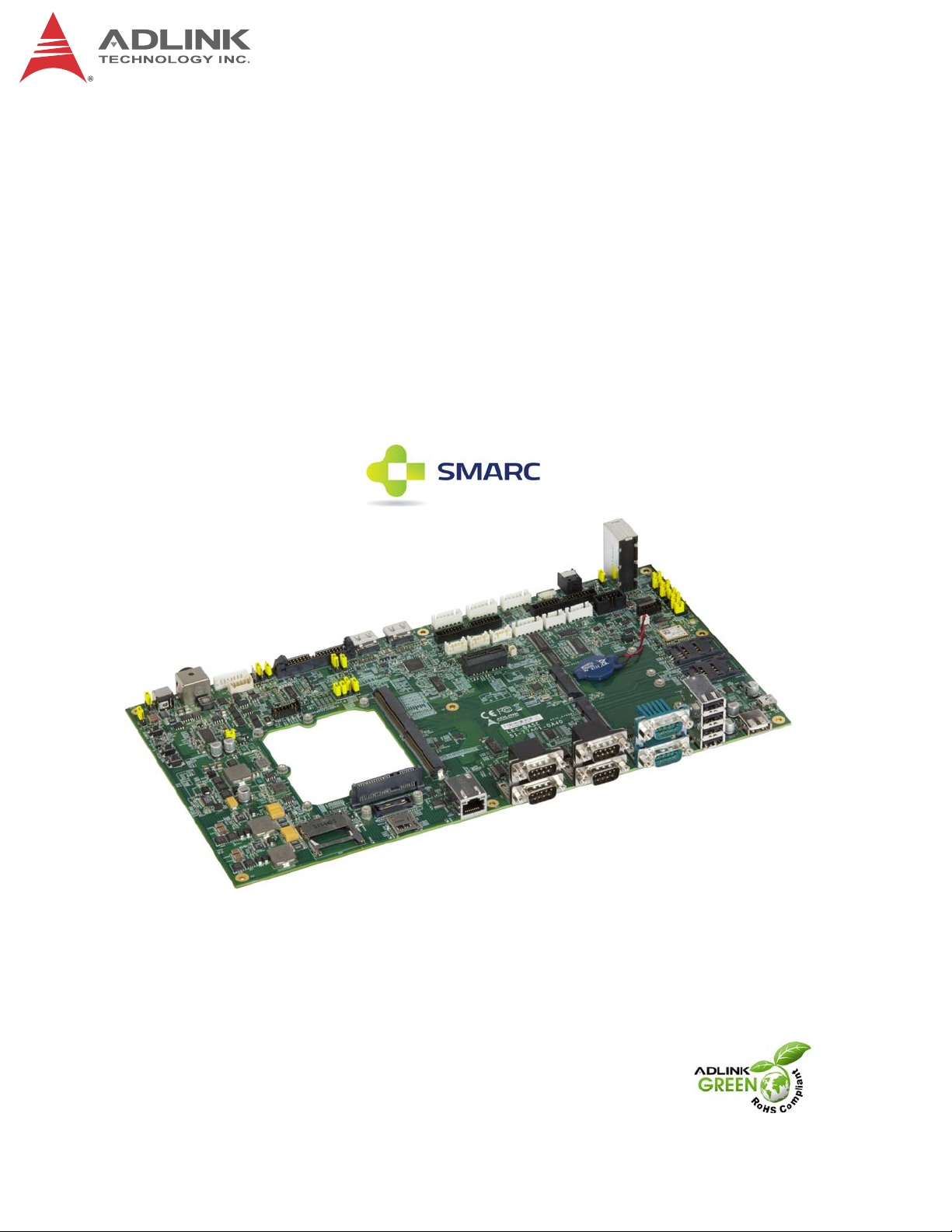
LEC-BASE
(SMARC Baseboard)
Technical Reference
P/N 50-1Z157-1010
Rev1.01
Advance Technologies. Automate the World.
Page 2
Disclaimer
Information in this document is provided in connection with ADLINK products. No license,
express or implied, by estoppel or otherwise, to any intellectual property rights is granted by
this document. Except as provided in ADLINK´s Terms and Conditions of Sale for such products, ADLINK assumes no liability whatsoever, and ADLINK disclaims any express or implied
warranty , relating to sale and/or use of ADLINK products including liability or warranties relating to fitness for a particular purpose, merchantability, or infringement of any patent, copyright or other intellectual property right. If you intend to use ADLINK products in or as medical
devices, you are solely responsible for all required regulatory compliance, including, without
limitation, Title 21 of the CFR (US), Directive 2007/47/EC (EU), and ISO 13485 & 14971, if
any . ADL INK may make changes to specifications and pr oduct descriptio ns at any time, with out notice.
Trademarks
MS-DOS, Windows, Windows 95, Windows 98, Windows NT and Windows XP are trademarks of Microsoft Corporation. PS/2 is a trademark of International Business Machines, Inc.
Intel and Solid State Drive are trademarks of Intel Corporation. PC/104 is a registered trademark of the PC/104 Consortium. All other trademarks appearing in this document are the
property of their respective owners. CoreModule is a registered trademark, and ADLINK, Little Board, LittleBoard, MightyBoard, MightySystem, MilSystem, MiniModule, ReadyBoard,
ReadyBox, ReadyPanel, RuffSystem, and ReadySystem are trademarks of ADLINK Technology, Inc. All other marks are the property of their respective companies.
Revision History
Revision Reason for Change Date
1000 Initial Release Dec/13
Revised board interface layout; updated interface pinout
1.01
tables; changed this document’s revision number from
1000 to 1.01
Apr/15
© Copyright 2013, 2014, 2015 ADLINK Technology, Incorporated
This document contains proprietary information protected by copyright. All rights are reserved.
No part of this manual may be reproduced by an y mechanical , electronic, or other means in any
form without prior written permission of the manufacturer
Audience
This manual provides reference only for computer design engineers, including but not limited
to hardware and software designers and applications engineers. ADLINK Technology, Inc.
assumes you are qualified to design and implement prototype computer equipment.
ii
Page 3

LEC-BASE
Environmental Responsibility
ADLINK is committed to fulfill its social responsibility to global environmental preservation
through compliance with the European Union's Restriction of Hazardou s Subst ances (RoHS)
directive and Waste Electrical and Electronic Equipment (WEEE) directive. Environmental
protection is a top priority for ADLINK. We have enforced measures to ensure that our products, manufacturing processes, components, and raw materials have as litt le impact on the
environment as possible. When products are at their end of life, our customers are encouraged to dispose of them in accordance with the product disposal and/or recovery programs
prescribed by their nation or company.
Important Safety Instructions
For user safety, please read and follow all Instructions, WARNINGs, CAUTIONs, and
NOTEs marked in this manual and on the associated equipment before handling/operating
the equipment.
Read these safety instructions carefully.
Keep this manual for future reference.
Read the specifications section of this manual for detailed information on the operating
environment of this equipment.
Turn off power and unplug any power cords/cables when installing/mounting or un-install-
ing/removing equipment.
To avoid electrical shock and/or damage to equipment:
Keep equipment away from water or liquid sources;
Keep equipment away from high heat or high humidity;
Keep equipment properly ventilated (do not block or cover ventilation openings) ;
Make sure to use recommended voltage and power source settings;
Always install and operate equipment near an easily accessible electrical socket-
outlet;
Secure the power cord (do not place any object on/over the power cord);
Only install/attach and operate equipment on stable surfaces and/or recommended
mountings; and,
If the equipment will not be used for long periods of time, turn off the power source and unplug
the equipment.
iii
Page 4

iv
Page 5

LEC-BASE
Table of Contents
1 Overview ........................................................................................................................... 1
1.1 Block Diagram........................................................................................................................ 1
1.2 Major Components (ICs)........................................................................................................ 2
1.3 Interface Headers, Jumper Headers, Switches, LEDs, and Connectors............................... 4
1.4 Specifications......................................................................................................................... 8
1.4.1 Physical Specifications ......................................................................................................8
1.4.2 Mechanical Specifications .................................................................................................8
2 Interface Signals...............................................................................................................9
2.1.1 SD/eMMC (AFB2) Interface ...... ... ................................................................................... 9
2.1.2 Camera 0 (CAM0)..................................... .... ... ... ... .... ... ... ... ....................................... ...10
2.1.3 Camera 1 (CAM1)..................................... .... ... ... ... .... ... ... ... ....................................... ...11
2.1.4 Camera 3 (CAM3)..................................... .... ... ... ... .... ... ... ... ....................................... ...11
2.1.5 Controller Area Network (CAN1)...................... ... ... .... ...................................... ... .... ... ...12
2.1.6 Cell Charger/Battery Supply (CN4) ...............................................................................12
2.1.7 GPIO1 ...........................................................................................................................13
2.1.8 Smart Battery (H25) ......... ... ... ... ... .... ... ... ... ....................................... ... .... ... ... ... ... .... ... ...13
2.1.9 I2S1...............................................................................................................................14
2.1.10 I2S2...............................................................................................................................14
2.1.11 I2S3...............................................................................................................................14
2.1.12 Alternate Function Block 1 (J9) .....................................................................................15
2.1.13 I2C (J10)................. ... ... .... ... ... ... ... .... ... ... ... .... ... ....................................... ... ... ... ... ..........16
2.1.14 Battery (J12)..................................................................................................................16
2.1.15 LVDS Control (J14) ................................... .... ... ... ... .... ... ... ... ....................................... ...16
2.1.16 TTL Panel Control (PC1)...............................................................................................16
2.1.17 Power Management (PW1)....................... .... ... ... ... .... ... ... ... ... .......................................17
2.1.18 SPI0...............................................................................................................................17
2.1.19 SPI1...............................................................................................................................17
2.1.20 LVDS.............................................................................................................................18
2.1.21 TTL................................................................................................................................19
Appendix A Technical Support ......................................................................................... 21
v
Page 6

vi
Page 7
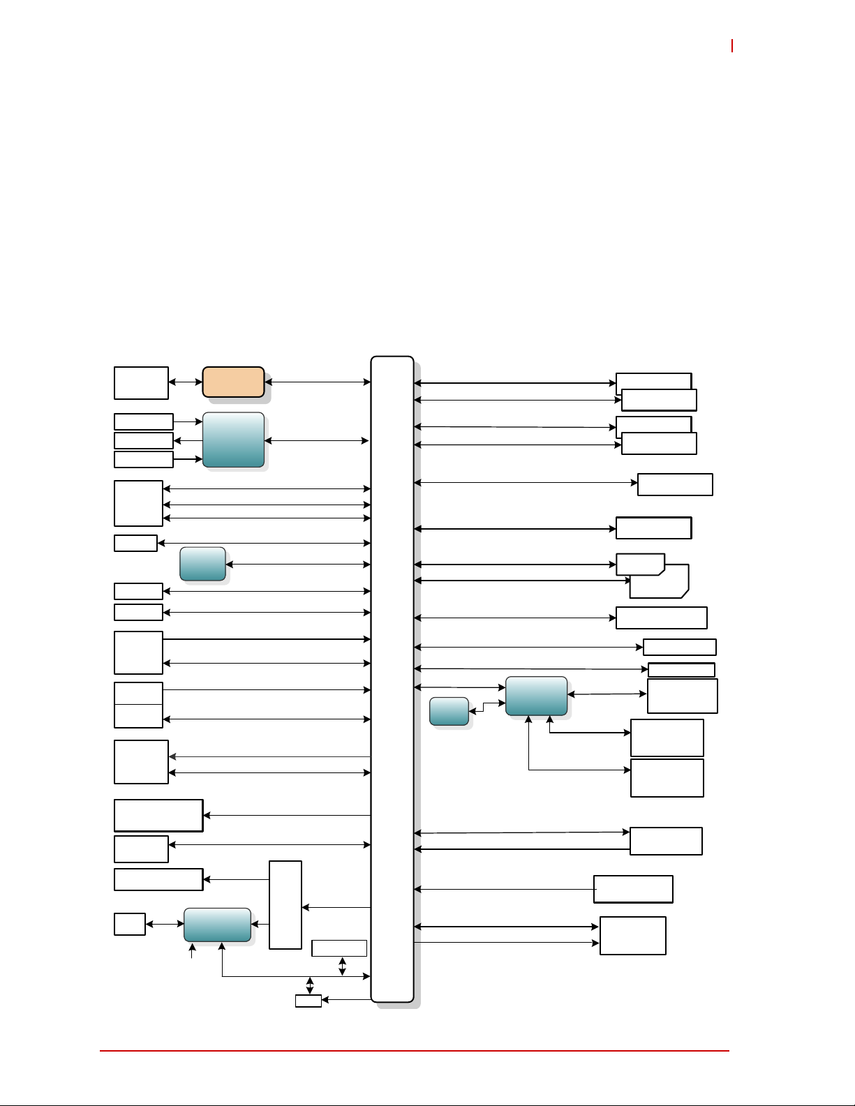
1 Overview
USB1_B
USB1_A
HDMI-J6
HDMI-R GB
SI L9022
Codec
TLV320AI
C23BPW
LAN
Transformer
314-pin Connector
USB0
USB2
USB1
USB 2.0
SPI1
Level Shift
buffers
HDMI
RGB 18/24-bit
Header
18/24-bit RGB TTL
GbE
RJ45
10/100/1000
SATA1
SATA Connector
eMMC/SD/SDIO 8-bit
Line OUT
Line IN
SPDIF
Header
SPI0
UART1 (4-pin)
UART3
(2
-pin)
UART4(2
-pin
)
DB9
Camera Input Control Signals
CAM3
I2C LCD
USB 2.0 OTG
PCIE_
A (x1
)
HDMI / (or DP)
Header
24-bit LVDS
SDMMC
SD/SDIO 4-bit
SDIO
CSI1 Camera Input
I
2
2
C CAM
I2S1
I2S1
I C GP
I2S2 / HDA
I2S3
SPDIF
Management Pins
MIC
DB9
UART2 (4-pin)
CAN1 (2-pin)
CSI0 Camera Input
LVDS 18/24-bit
Header
I2C HDMI_CTRL
USB 2.0
(4 ports)
PC1
Header
Vdd, BKL_EN, BKL_CTRL
Boot Select / Force Recovery
DIP switch (4)
Test point
Header
Watchdog Time Out
GPIO (12-pin)
miniPCIe x1
A Slot
PCIe x1 Slot
PCIE_WAKE#
Power ena ble /
disable jumper
DB9
DB9
Header
Header
USB HUB
SMSC
USB2514i
USB
1
_C
miniPCIe x1
B Slot
DB9 (Dual)
GPS
Neo6
USB1_D
G Sensor
MMA7660FCT
EEPROM 4K
RTC
VRTC
I2C_HDMI
LEC_BASE_blkDiag_b
CAM0
CAM1
This initial manual version presents a general overview of the LEC-BASE baseboard including
the signal definitions of the non-standard user interfaces on the board. After reviewing this document you should understand the following features of the LEC-BASE.
Functional Block Diagram
Major Component (IC) Locations and Descriptions
Connector Locations and Descripti on s
Specifications
Non-Standard User Interface Signal Definitions (support is dependent on the specific
SMARC module; refer to the specific SMARC module manual for details)
1.1 Block Diagram
Figure 1-1 presents a functional representation of the baseboard.
LEC-BASE
Overview 1
Figure 1-1: Functional Block Diagram
Page 8
1.2 Major Components (ICs)
Table 1-1 lists the major integrated circuits on the LEC-BASE, including a brief description of
each IC. Figure 1-2 shows the locations of the major ICs.
Table 1-1: Major Integrated Circuit Descriptions and Functions
Chip Type Mfg. Model Description Function
G-Sensor (U4) Freescale
Semicondu
ctor
Touch Panel
Controller
(U18)
I2C, 2-wire
EEPROM
(U19)
CAN
Transceiver
(U25, U26)
I2S Audio
CODEC (U27)
Real Time
Clock (U36)
GPS Module
(U136)
Texas
Instruments
Atmel AT24C08C 2-wire, 8Kb serial
Texas
Instruments
Texas
Instruments
Maxim DS1337S I2C Serial Real-Time
u-blox NEO-Q-0 GPS Receiver,
MMA7660FC 3-axis Orientation/
Motion Detection
Sensor, connected to
the I2C GP interface at
pins S48 and S49 of
the SMARC connector.
The I2C address is
0x4C/0x4D.
TSC2046 Low-Voltage Touch
Controller, connected
to the SPIO interface
at pins P43, P44, P45,
and P46 of the
SMARC connector.
EEPROM, connected
to the I2C LCD
interface at pins S139
and S140 of the
SMARC connector.
The I2C address is
0xA8/0xA9.
SN65HVDA540QDR Transceiver for
Controller Area
Network, connected to
the CAN0 and CAN1
interfaces at pins
P143, P144, P145,
and P146 of the
SMARC connector.
TLV320AIC23B I2S Stereo Audio
CODEC, connected to
the I2S0 interface at
pins S39, S40, S41,
S42 of the SMARC
connector.
Clock, connected to
the I2C LCD interface
at pins S139 and S140
of the SMARC
connector. The I2C
address is 0xD0/0xD1.
connected over the
USB hub to the
SMARC connector at
pins P65 and P66.
Senses data
changes, product
orientation, and
gestures through
an interrupt (INT)
pin.
Senses 4-wire
resistive touch
screen.
Provides storage
for baseboard
parameters
through the I
LCD pins, S139
and S140, on the
SMARC module.
Provides up to 1
Mbps of
differential
transmit and
receive
capabilities for the
CAN controller in
the CPU.
Supports
data-transfer word
lengths of 16, 20,
24, and 32 bits
with sample rates
from 8kHz to
96kHz.
Provides
low-power clock/
calendar with two
programmable
time-of-day
alarms and a
programmable
square-wave
output
Provides
6-positioning
engine for parallel
time/frequency
space searches
2
C
2 Overview
Page 9
LEC-BASE_Top_Comp_b
U18
U4
U19
U36
U26
U25
U27
U136
Key:
U4 - G-Sensor
U18 - Touch Panel Controller
U19 - I2C EEPROM
U25, U26 - CAN Transceivers
U27 - Audio CODEC
U36 - Real Time Clock
U136 - GPS Module
LEC-BASE
Figure 1-2: Component Locations (Top Side)
Overview 3
Page 10

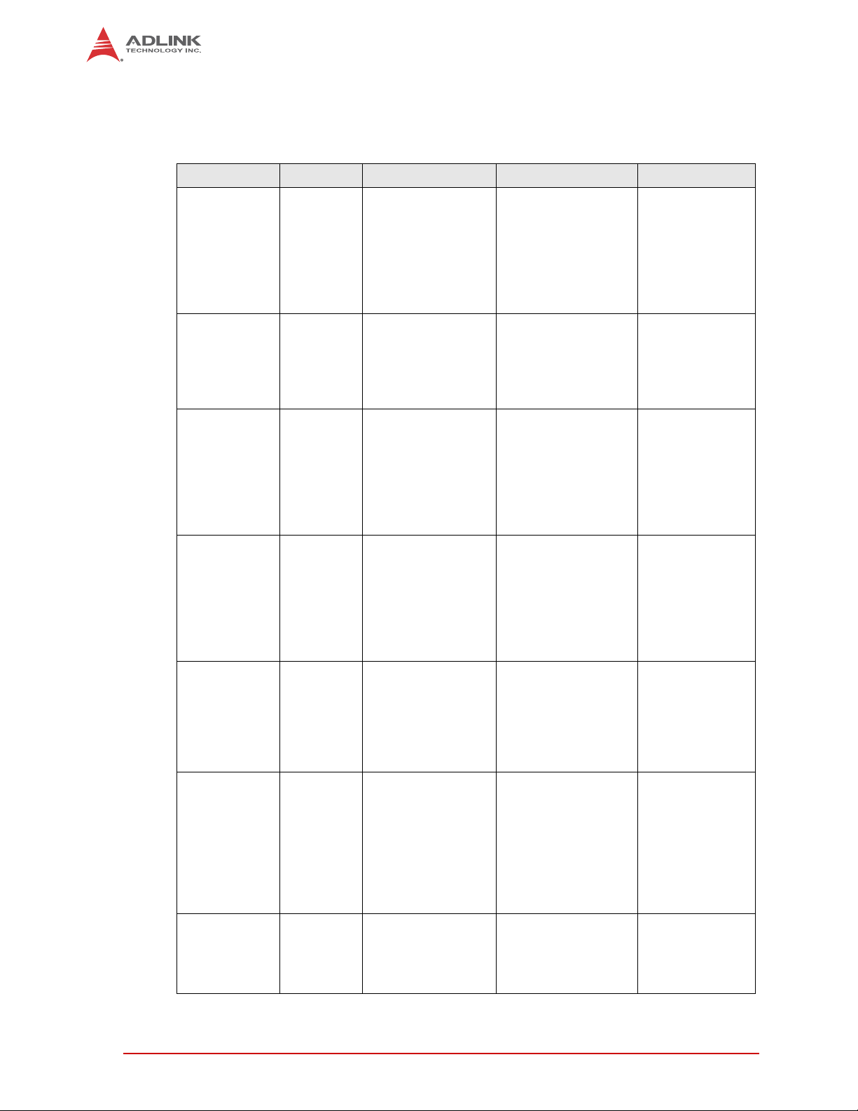
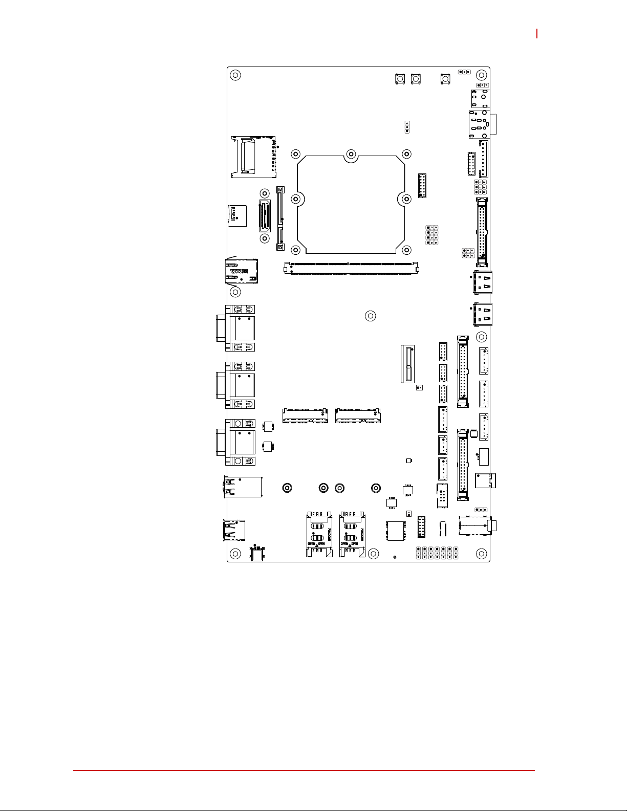
1.3 Interface Headers, Jumper Headers, Switches, LEDs, and Connectors
Table 1-2 describes the headers, switches, LEDs, and connectors for the LEC-BASE baseboard
shown in Figure 1-3.
Table 1-2: Header, Switch, LED, and Connector Descriptions
Header /
Connector#
AFB2 SD/eMMC Card 60-pin terminal for eMMC card
AJ1 Audio Jack 32-pin standard audio jack for three audio interfaces: Line
ANT1 GPS Antenna 3-pin, radio frequency, 50 ohm antenna for receiving GPS
CAM0 Camera 10-pin header for MIPI CSI1 camera
CAM1 Camera 10-pin header for MIPI CSI0 camera
CAM3 Camera Control 10-pin header for I2C clock/data signals on MIPI CSI
CAN1 (two
ports)
CN1 Touch Screen 4-pin, standard connector for 4-wire resistive touch
CN2 microSD 12-pin, standard socket for microSD memory cards
CN4 Cell Charger/Battery
CN5 MiniDin DC Jack 4-pin, female connector for additional power input for
COM1 (two
ports)
COM2 (two
ports)
GPIO1 GPIO 12-pin header for General Purpose IO
H25 Battery2 9-pin header for smart battery connection
I2S1 I2S Devices 6-pin header for I2S devices such as audio CODECs,
I2S2 I2S Devices 6-pin header for I2S devices such as audio CODECs,
I2S3 I2S Devices 6-pin header for I2S devices such as audio CODECs,
J1 SMARC Interface 314-pin, MXM socket for Memory, Video, and I/O functions
J3 TTL 34-pin header for VGA LCD flat panel output
J6 HDMI1 19-pin, standard HDMI micro connector
J8 LVDS 34-pin header for LVDS output
J9 (AFB1) Auxiliary Devices 34-pin header for differential pair and data bit signals
J10 I2C 2-pin header for general purpose, level-shifted 3.3V, I2C
J11 HDMI2 19-pin, standard HDMI micro connector
J12 Battery 2-pin header for RTC external battery
J14 LVDS Control 8-pin head er for LVDS panel and backlight control
JACK1 DC Power 6-pin, standard, right-angle 19V center-pin, DC power jack
JP2 LCD Power Select 3-pin, jumper header for LCD 3.3V (1-2) or 5V (2-3) power
JP3 I2C Select 3-pin, jumper header to select I2C_LCD (clock/data pair)
Signal / Device Description
In (Blue), Line Out (Green), and MIC In (Pink)
signals
camera
CAN Bus Dual, 9-pin standard DB9 connectors for transmitting and
receiving Controller Area Network signals
controller (not for TTL USB-based touch screen controller
in Starter Kit)
12-pin header for 2-cell, raw lithium ion battery interface to
Supply
UART Dual, 9-pin standard DB9 connectors for RS232 serial
UART Dual, 9-pin standard DB9 connectors for RS232 serial
power the baseboard
auxiliary circuitry
ports
ports
baseband modems, and touch controllers
baseband modems, and touch controllers
baseband modems, and touch controllers (designated also
for HD Audio CODECs)
clock and data signals for the module
selection
for HDMI controller (1-2 default)
4 Overview
Page 11

LEC-BASE
Table 1-2: Header, Switch, LED, and Connector Descriptions (Continued)
JP4 Battery Charger
Enable
JP5 Cell Charger Present 3-pin jumper header to accept charging (1-2 if cell present;
JP6 Cell Charger Voltage 3-pin jumper header for I2C voltage selection (pins 2-3 for
JP7 Cell Protection IC, I2C
Signal Pair
JP8 LCD/LVDS Select
(High = 1-2; Low = 2-3)
JP9 LCD/LVDS Select
(High = 1-2; Low = 2-3)
JP10 LVDS 3-pin jumper header for selecting strobe for LVDS
JP11 LVDS 3-pin jumper header for powering ON/OFF LVDS
JP12 LVDS Backlight
Control (for J14)
JP13 LVDS Panel Control
(for J14)
JP14 LVDS Backlight
Control (for J14)
JP15 I2C Select (related to
JP3)
JP16 Boot Select 0 3-pin jumper header for Boot Select Switch SW1 pins 1
JP17 Boot Select 1 3-pin jumper header for Boot Select Switch SW1 pins 1
JP18 Boot Select 2 3-pin jumper header for Boot Select Switch SW1 pins 1
JP19 Boot Select Force
Recovery
JP20 VIO Select (IO
Voltage)
JP21 DC-OUT 3-pin jumper header to override (1-2) or not override (2-3)
LAN1 Ethernet 8-pin, standard RJ45 jack for Gigabit Ethernet port
LED1 USB Green LED indicating USB is operational
LED2 Mini PCIE1 Green LED indicating WAN
LED3 Mini PCIE2 Green LED indicating WAN
LED4 nLID Green LED indicating active low LID signal is asserted
LED5 nSLEEP Green LED indicating active low SLEEP signal is asserted
LED6 nBATLOW Green LED indicating active low BATLOW signal is
LED7 SATA Green LED indicating SATA activity
LED8 SD Card Green LED indicating over current on SD card
LED9 USB Green LED indicating USB is operational
LED11 Cell Protection IC Green LED indicating battery pack conditions
3-pin jumper header for enabling the smart battery/cell
charger: ON (1-2) or OFF (2-3)
2-3 if cell not present)
2.5V or pins 1-2 for 3.3V) between cell and charger
3-pin header to allow Texas Instruments software to
communicate with the cell protection IC: 1=Data, 2=Clock,
and 3=GND
3-pin jumper header to make selection between LCD and
LVDS (JP9 Low and JP8 High = LVDS; JP9 High and JP8
Low = LCD; JP9 High and JP8 High = None)
3-pin jumper header to make selection between LCD and
LVDS (JP9 Low and JP8 High = LVDS; JP9 High and JP8
Low = LCD; JP9 High and JP8 High = None)
converter: rising edge 1-2, falling edge 2-3
controller: ON 1-2, OFF 2-3
3-pin jumper header for backlight power management to
select 3V (1-2) or 5V (2-3)
3-pin jumper header for panel power to select 3V (1-2) or
5V (2-3)
3-pin jumper header for backlight power management to
select 12V (1-2) or 5V (2-3)
3-pin jumper header tor selecting I2C_HDMI for HDMI
controller (2-3 Default)
and 8 (Pins 2-3 to ground boot_sel0; pins 1-2 to float
boot_sel0)
and 8 (Pins 2-3 to ground boot_sel1; pins 1-2 to float
boot_sel1)
and 8 (Pins 2-3 to ground boot_sel2; pins 1-2 to float
boot_sel2)
3-pin jumper header for Boot Select Switch SW1 pins 4
and 5 (Pins 2-3 to ground force_recover; pins 1-2 to float
force_recover)
3-pin jumper header for VIO 1.8V (1-2) [no other option is
valid, as defined by the SMARC specification]
power button (PWRON1) for automatic Power On testing
asserted
Overview 5
Page 12

Table 1-2: Header, Switch, LED, and Connector Descriptions (Continued )
LED12 Cell Protection IC Green LED indicating battery pack conditions
LED13 Cell Protection IC Green LED indicating battery pack conditions
LED14 Cell Protection IC Green LED indicating battery pack conditions
LED15 Cell Protection IC Green LED indicating battery pack conditions
LED16 Power Green LED indicating power asserted to baseboard
MINIPCIE1 PCIE Mini Card 52-pin, standard, right-angle socket for PCI Express Mini
Card
MINIPCIE2 PCIE Mini Card 52-pin, standard, right-angle socket for PCI Express Mini
Card
PC1 TTL Panel Control 6-pin header for control signals to flat panel display
PCIE1 PCI Express 36-pin, standard edge connector for x1 PCI Express
interface
PWM1 Power Management 14-pin header for Power Management signals
PWRON1 Power On 4-pin, push-button switch to turn on 12V to baseboard
PWRON2 Power On 4-pin, push-button switch to assert POWER_nBTN signal
for SMARC connector
SATA1 SATA 7-pin, standard Serial ATA connector with attached 15-pin
power connection
SD2 SD Card Slot Standard slot connector for Secure Digital memory card
SIM1 SIM Slot Standard slot connector for Subscriber Identity Module
SIM2 SIM Slot Standard slot connector for Subscriber Identity Module
SPDIF1 SPDIF-OUT Audio Standard connector for SPDIF digital audio interface
SPI0 System Packet
Interface
SPI1 System Packet
Interface
SW15 Reset Switch Push-button switch to warm reset the module
USBC1 USB 4-stack, standard USB 2.0 connector
USB1 Micro-USB Standard connector for micro-USB interface, OTG
USB2 USB Standard connector for single USB 2.0 interface
5-pin header for SPI interface
4-pin header for SPI interface
6 Overview
Page 13

JACK1
PWRON1
PWRON2
SD2
LED8
LED16
LED2
LED1
LED3
LED9
MINIPCIE1 MINIPCIE2
LED7
CN2
H25
CN4
LAN1
COM1
COM2
CAN1
USBC1
USB2
USB1
SIM1
SIM2
JP13
SPI0
SPI1
PC1
CAM3
CAM1
CAM0
PCIE1
J3
J10
J12
LED6
LED5
LED4
J8
J14
AJ1
SPDIF1
JP12
CN1
I2S3
I2S2
I2S1
J11
J1
S1
P1
J6
J9
(AFB1)
AFB2
SATA 1
JP2
JP14
JP8
JP9
CN5
JP4
JP20
JP15
JP7
JP6
JP5
JP3
LED15
LED14
LED13
LED12
LED11
PWM1
JP21
JP10
JP11
ANT1
GPIO1
SW15
LEC-BASE_Baseboard_Top_Conn_c
JP19
JP18
JP17
JP16
Key:
AFB2 - Alternate Function Block 2
AJ1 - Audio Jack
ANT1 - GPS Antenna
CAM0 - Camera 0
CAM1 - Camera 1
CAM3 - Camera 3
CAN1 - Controller Area Network (Dual Ports)
CN1 - 4-wire Resistive Touch Controller
CN2 - microSD (8 bits)
CN4 - Cell Charger/Battery Supply
CN5 - MiniDin DC Jack
COM1 - UART (Dual Ports)
COM2 - UART (Dual Ports)
PC1 - TTL Panel Control
PCIE1 - PCI Express
PWM1 - Power Management
PWRON1 - Power On
PWRON2 - Power On
SATA1 - SATA
SD2 - SD Card Slot
SIM1 - SIM Slot
SIM2 - SIM Slot
SPDIF1 - SPDIF OUT
SPI0 - System Packet Interface
SPI1 - System Packet Interface
SW15 - Reset Switch
USBC1 - USB
USB1 - Micro USB
USB2 - USB
NOTE: The larger black pins
each represent pin 1
LAN1 - Ehternet
LED1 - USB
LED2 - Mini PCIE1
LED3 - Mini PCIE2
LED4 - nLID
LED5 - nSLEEP
LED6 - nBATLOW
LED7 - SATA
LED8 - SD Card (4 bits)
LED9 - USB
LED11 - Cell Protection IC
LED12 - Cell Protection IC
LED13 - Cell Protection IC
LED14 - Cell Protection IC
LED15 - Cell Protection IC
LED16 - Power
MINIPCIE1 - PCIe Mini Card
MINIPCIE2 - PCIe Mini Card
JP4 - Battery Charger Enable
JP5 - Cell Charger Present
JP6 - Cell Charger Voltage
JP7 - Cell Protection IC
JP8 - LCD/LVDS Select
JP9 - LCD/LVDS Select
JP10 - LVDS Strobe
JP11 - LVDS Controller
JP12 - LVDS Backlight Control
JP13 - LVDS Panel Control
JP14 - LVDS Backlight Control
JP15 - Select I2C_HDMI for J11
JP16 - Boot Select
JP17 - Boot Select
JP18 - Boot Select
JP19 - Boot Select Recovery
JP20 - VIO Select
JP21 - DC-OUT
GPIO1 - General Purpose IO
H25 - Smart Battery
I2S1 - I2S 1
I2S2 - I2S 2
I2S3 - I2S 3
J1 - SMARC Interface
J3 - TTL LCD
J6 - HDMI1
J8 - LVDS LCD
J9 - Alternate Function Block 1
J10 - I2C
J11 - HDMI2
J12 - External Battery (RTC backup)
J14 - LVDS Control
JACK1
- DC Power In
JP2 - LCD Power Select
JP3 - Select I2C_LCD for J11
Figure 1-3: Connector Locations (Top Side)
LEC-BASE
Overview 7
Page 14

1.4 Specifications
6.89" (175mm)
2.32" (59mm)
6.73" (171mm)
12.99" (330mm)
LEC-BASE_Top_MechDmn_b
1.4.1 Physical Specifications
Table 1-3 lists the physical dimensions of the baseboard.
Table 1-3: Weight and Footprint Dimensions
Item Dimension
Weight 0.42 kg (0.93 lb)
Height (overall) 33.02 mm (1.30 inches)
Board thickness 2.03 mm (0.08 inches)
Width 175.00 mm (6.89 inches)
Length 330.00 mm (12.99 inches)
1.4.2 Mechanical Specifications
Overall height is measured from the upper board
surface to the top of the highest permanent
component on the upper board surface. This
measurement does not include the cooling solution,
which can vary. The cooling solution will probably
increase this dimension.
Figure 1-4: Mechanical Dimensions (Top Side)
8 Overview
Page 15

2 Interface Signals
This section provides the pin signals for all the non-standard user interfaces on the LEC-BASE.
Signal definitions for standard interfaces such as SATA, USB, PCIe, and DB9 serial connectors
can be found in their respective specification data sheets.
NOTE: The tables in this section define pin sequence using the method in the following example: A 10-pin header with two rows of pins, using odd/even numbering, where pin 2 is directly
across from pin 1, is noted as 10 pins, 2 rows, odd/even pin sequence (1, 2).
2.1.1 SD/eMMC (AFB2) Interface
Table 2-4 lists the pin signals of the SD Card ground plane socket, which provides 60-pins, 2
rows, odd/even pin sequence (1, 2) with 0.02" (0.50mm) pitch. These signals are connected to
the SD/eMMC interface at pins S26 through S36 of the SMARC connector over a 3.3 volt level
shifter.
T able 2-4: SD/eMMC (AFB2) Interface Pin Signals
Pin # Signal
1
2 GND
3 MMC2_D0_3V
4
5
6 GND
7
8
9 MMC2_D1_3V
10
11
12 GND
13
14
15 MMC2_D2_3V
16
17
18
19
20
21 MMC2_D3_3V
22
23
24
25
26
27 MMC2_D4_3V
28
29
30 GND
31
32
33 MMC2_D5_3V
34
35
GND
GND
GND
GND
GND
GND
GND
GND
GND
GND
GND
GND
GND
GND
VDD_3V3
GND
GND
GND
GND
VDD_3V3
GND
GND
GND
GND
GND
LEC-BASE
Interface Signals 9
Page 16

Table 2-4: SD/eMMC (AFB2) Interface Pin Signals (Continued)
36 GND
37 GND
38
39 MMC2_D6_3V
40
41
42
43 GND
44
45 MMC2_D7_3V
46
47
48
49 GND
50
51 MMC2_CK_3V
52
53
54
55 GND
56
57 MMC2_CMDD_3V
58
59 GND
60
GND
GND
GND
GND
GND
GND
GND
GND
GND
GND
GND
GND
GND
GND
GND
NOTE: The shaded table cells denote power or ground.
2.1.2 Camera 0 (CAM0)
Table 2-5 lists the pin signals of the Camera0 header, which provides 10-pins, 2 rows, odd/even
pin sequence (1, 2) with 0.079" (2.00mm) pitch. These signals are connected directly to the MIPI
CSI camera interface at the SMARC connector.
Table 2-5:Camera 0 Pin Signals (CAM0)
Pin # Signal
1 CSI1_CK+
2 CSI1_CK3 CSI1_D0+
4 CSI1_D05 CSI1_D1+
6 CSI1_D17 CSI1_D2+
8 CSI1_D29 CSI1_D3+
10 CSI1_D3-
10 Interface Signals
Page 17

LEC-BASE
2.1.3 Camera 1 (CAM1)
Table 2-6 lists the pin signals of the Camera1 header, which prov id es 1 0- pins, 2 rows , od d/even
pin sequence (1, 2) with 0.079" (2.00mm) pitc h. These signals are connected to the camera
control signals at the SMARC connector.
Table 2-6: Camera 1 Pin Signals (CAM1)
Pin # Signal
1 CSI0_CK+
2 CSI0_CK3 CSI0_D0+
4 CSI0_D05 CSI0_D1+
6 Not Connected
7 CSI0_D18 Not Connected
9
10
GND
GND
NOTE: The shaded table cells denote ground.
2.1.4 Camera 3 (CAM3)
Table 2-7 lists the pin signals of the Camera 3 header, which provides 10-pins, 2 rows, odd/even
pin sequence (1, 2) with 0.079" (2.00mm) pitc h. These signals are connected to the camera
control signals at the SMARC connector.
Table 2-7: Camera 3 Pin Signals (CAM3)
Pin # Signal
1 CAM0_nPWR
2 I2C_CAM_CLK_1.8V
3 Not Connected
4 I2C_CAM_DATA_1.8V
5 Not Connected
6 Not Connected
7 CAM0_nRST_3V over the 3.3V level shifter
8 Not Connected
95 Volt
10 Not Connected
Interface Signals 11
Page 18

2.1.5 Controller Area Network (CAN1)
Table 2-8 and T able 2-9 list the pin signals of the Controller Area Network interface (CAN1A and
CAN1B), which provides standard dual DB9 connectors.
Table 2-8: Controller Area Network Signals (CAN1A)
Pin # Signal
1
2CAN1_H
3
4
5
6
7CAN1_L
8
9
NOTE: These pins are connected over the CAN transceiver to the CAN0 SMARC connector
interface (pins P143 and P144.)
Pin # Signal
1
2CAN2_H
3
4
5
6
7CAN2_L
8
9
Not Connected
Not Connected
Not Connected
GND
Not Connected
Not Connected
5 Volt
Table 2-9: Controller Area Network Signals (CAN1B)
Not Connected
Not Connected
Not Connected
GND
Not Connected
Not Connected
5 Volt
NOTE: These pins are connected over the CAN transceiver to the CAN1 SMARC connector
interface (pins P145 and P146.)
2.1.6 Cell Charger/Battery Supply (CN4)
Table 2-10 lists the pin signals of the Cell Charger/Battery Supply header, which provides 12
pins in 2 rows, odd/even pin sequence (1, 2), and 0.079" (2.00mm) pitch.
Table 2-10: Cell Charger/Battery Supply (CN4)
Pin # Signal
1
2+VE
3
4
5
6
7
8
9
10
11
12
Therm1
Cell_4 (positive terminal of); connected to pins 2, 4, 6
+VE
Cell_3 (positive terminal of)
+VE
Cell_2
(positive terminal of)
-VE
Cell_1 (positive terminal of)
-VE
-VE (negative terminal of); connected to pins 8, 10, 12
-VE
12 Interface Signals
Page 19

LEC-BASE
2.1.7 GPIO1
Table 2-11 lists the pin signals of the General Purpose IO header, which provides 12 pins in 2
rows, odd/even pin sequence (1, 2), and 0.079" (2.00mm) pitch. These pins are connected to
the SMARC connector over the 3.3 volt level shifter.
Ta bl e 2-11: General Purpose IO (GPIO1)
Pin # Signal
1
2
3
4
5
6
7
8
9
10
11
12
GPIO_28_3V (connected to SMARC pin P119)
CAM0_nPWREN_3V
(connected to SMARC pin P108)
GPIO_29_3V (connected to SMARC pin P112)
CAM1_nPWREN_3V
(connected to SMARC pin P109)
GPIO_177_3V (connected to SMARC pin P116)
CAM0_nRST_3V (connected to SMARC pin P110)
GPIO_54_3V (connected to SMARC pin P117)
CAM1_nRST_3V
(connected to SMARC pin P111)
GPIO_55_3V (connected to SMARC pin P113)
CAM_FLD_3V
(connected to SMARC pin P115)
GPIO_56_3V (connected to SMARC pin P114)
GPIO_27_3V (connected to SMARC pin P118)
NOTE: Signal names relative only to the LEC-3517 module.
2.1.8 Smart Battery (H25)
Table 2-12 lists the pin signals of the Smart Battery header, which provides 9 pins in a single row
with 0.079" (2.00mm) pitch. These signals are connected to and controlled by the onboard
LTC1760 smart battery charger controller.
Table 2-12: Smart Battery (H25)
Pin # Signal
1
2
3
4
5
6 TH1 (Thermistor Force/Sense connection to LTC1760 charger controller)
7
8 GND
9
NOTE: Shaded table cells denote ground.
+VE (battery and charging voltage)
+VE (battery and charging voltage)
+VE (battery and charging voltage)
1760_SCL1
(I2C bus from LTC1760 charger controller)
1760_SDA1 (I2C bus from LTC1760 charger controller)
GND
GND
Interface Signals 13
Page 20

2.1.9 I2S1
Table 2-13 lists the pin signals of the I2S1 header, which provides 6 pins in a single row with
0.098" (2.50mm) pitch. These pins are connected to the SMARC connector over the 3.3 volt
level shifter.
Table 2-13: I2S1 Signals (I2S1)
Pin # Signal
1
2
3
4
5
6
VDD_3V3
MCBSP1_FSX_3V (connected to SMARC pin S39)
MCBSP1_DX_3V (connected to SMARC pin S40)
MCBSP1_DR_3V (connected to SMARC pin S41)
MCBSP1_CLKX_3V (connected to SMARC pin S42)
GND
NOTE: Shaded table cells denote power or ground.
2.1.10 I2S2
Table 2-14 lists the pin signals of the I2S2 header, which provides 6 pins in a single row with
0.098" (2.50mm) pitch. These pins are connected to the SMARC connector over the 3.3 volt
level shifter.
Table 2-14: I2S2 Signals (I2S2)
Pin # Signal
1
2
3
4
5
6
VDD_3V3
MCBSP2_FSX_3V (connected to SMARC pin S43)
MCBSP2_DX_3V (connected to SMARC pin S44)
MCBSP2_DR_3V (connected to SMARC pin S45)
MCBSP2_CLKX_3V (connected to SMARC pin S46)
GND
NOTE: Shaded table cells denote power or ground.
2.1.11 I2S3
Table 2-15 lists the pin signals of the I2S3 header, which provides 6 pins in a single row with
0.098" (2.50mm) pitch. These pins are connected to the SMARC connector over the 3.3 volt
level shifter.
Table 2-15: I2S3 Signals (I2S3)
Pin # Signal
1
2
3
4
5
6
NOTE: Shaded table cells denote power or ground.
VDD_3V3
MCBSP3_FSX_3V (connected to SMARC pin S50)
MCBSP3_DX_3V (connected to SMARC pin S51)
MCBSP3_DR_3V (connected to SMARC pin S52)
MCBSP3_CLKX_3V (connected to SMARC pin S53)
GND
14 Interface Signals
Page 21

LEC-BASE
2.1.12 Alternate Function Block 1 (J9)
Table 2-16 lists the pin signals of the Alternate Function Block 1 header which provides 34-pins,
2 rows, odd/even pin sequence (1, 2) with 0.079" (2.0mm) pitch. These pins are connected
dirctly to the SMARC connector.
Table 2-16: Alternate Function Block 1 Interface Pin Signals (J9)
Pin # Signal
1
2 VDD_5V
3
4 GND
5
6
7
8
9
10 GND
11
12
13
14
15 GND
16 GND
17
18
19 GND
20
21
22 GND
23
24
25
26
27
28 GND
29 GND
30
31
32
33
34 GND
VDD_5V
AFB0_OUT (connected to SMARC pin S17)
GND
AFB_DIFF0+ (connected to SMARC pin S62)
AFB1_OUT
AFB_DIFF0AFB2_OUT
GND
AFB_DIFF1+ (connected to SMARC pin S65)
AFB3_IN
AFB_DIFF1-
AFB4_IN (connected to SMARC pin S21)
AFB_DIFF2+
AFB_DIFF2AFB5_IN
GND
AFB_DIFF3+
AFB6_PTIO
AFB_DIFF3AFB7_PTIO
AFB_DIFF4+
AFB8_PTIO
AFB_DIFF4AFB9_PTIO
(connected to SMARC pin S18)
(connected to SMARC pin S63)
(connected to SMARC pin S19)
(connected to SMARC pin S20)
(connected to SMARC pin S66)
(connected to SMARC pin S68)
(connected to SMARC pin S69)
(connected to SMARC pin S22)
(connected to SMARC pin S71)
(connected to SMARC pin S23)
(connected to SMARC pin S72)
(connected to SMARC pin S24)
(connected to SMARC pin S74)
(connected to SMARC pin S55)
(connected to SMARC pin S75)
(connected to SMARC pin S56)
NOTE: The shaded table cells denote ground or power.
Interface Signals 15
Page 22

2.1.13 I2C (J10)
Table 2-17 lists the pin signals of the I2C header, which provides 2 pins with 0.049" (1.25mm)
pitch. These pins are connected to the SMARC connector over the 3.3 volt level shifter.
Table 2-17: I2C Signals (J10)
Pin # Signal
1
2
I2C_GP_DAT_3V (connected to SMARC pin S48)
I2C_GP_CK_3V (connected to SMARC pin S49)
2.1.14 Battery (J12)
Table 2-18 lists the pin signals of the battery header, which provides 2 pins with 0.049"
(1.25mm) pitch.
Table 2-18: Battery Signals (J12)
Pin # Signal
1
2
V_RTC
GND
NOTE: Shaded table cells denote power or ground.
2.1.15 LVDS Con trol (J14)
Table 2-19 lists the pin signals of the Smart Battery header, which provides 8 pins in two rows
with odd/even pin sequence (1,2) and 0.01" (2.54mm) pitch.
Table 2-19: LVDS Control Signals (J14)
Pin # Signal
1
2
3
4 GND
5
6 GND
7
8
GND
PNLPWR (display supply voltage, selectable with JP13)
LVDS_BKL_CTRL (backlight control, selectable with JP12)
LCD_nEN (backlight enable)
Not Connected
BLPWR
(backlight supply voltage, selectable with JP14)
NOTE: Shaded table cells denote ground.
2.1.16 TTL Panel Control (PC1)
Table 2-20 lists the pin signals of the TTL Panel Control header, which provides 6 pins in a single row with 0.098" (2.50mm) pitch. These pins are connected directly to the display control pins
at the SMARC connector.
Table 2-20: LVDS Control Signals (PC1)
Pin # Signal
1
2
3
4 Not Connected
5 Not Connected
6 LCD_RESET (Active Low)
LCD_DE (connected over the 3.3 volt level shifter)
LCD_BKLT_PWM
LCD_VDD_EN
16 Interface Signals
Page 23

LEC-BASE
2.1.17 Power Management (PW1)
Table 2-21 lists the pin signals of the Power Management header, which provides 14 pins in 2
rows, odd/even pin sequence (1, 2), and 0.079" (2.00mm) pitch. These pins are connected
directly to the Power Management pins at the SMARC connector.
Table 2-21: Power Management Signals (PWM1)
Pin # Signal
1
2 VIN_PWR_nBAD
3
4 nCHARGING
5
6 CHARGE_nPRSNT
7
8 CHARGE_nSTBY
9
10 CARRIED_PWR_ON
11
12
13 GND
14
WDT_TIME
nLID
nSLEEP
nBATLOW
nTEST
Not Connected
Not Connected
GND
NOTE: Shaded table cells denote ground.
2.1.18 SPI0
Table 2-22 lists the pin signals of the System Packet Interface 0 header, which provides 5 pins in
a single row with 0.098" (2.50mm) pitch. These pins are connected to the SMARC connector
over the 3.3 volt level shifter.
Table 2-22: System Packet Interface 0 Signals (SPI0)
Pin # Signal
1
2
3
4
5
SPI2_CLK_3V (connected to SMARC pin P56)
SPI2_SOMI_3V (connected to SMARC pin P57)
SPI2_SIMO_3V (connected to SMARC pin P58)
SPI2_CS0_3V
SPI2_CS1_3V
(connected to SMARC pin P54)
(connected to SMARC pin P55)
NOTE: The signals for this header are defined by the module CPU as “SPI2”, but the header is
labelled “SPI0” on the board.
2.1.19 SPI1
Table 2-23 lists the pin signals of the System Packet Interface 1 header, which provides 4 pins in
a single row with 0.098" (2.50mm) pitch. These pins are connected to the SMARC connector
over the 3.3 volt level shifter.
Table 2-23: System Packet Interface 1 Signals (SPI1)
Pin # Signal
1
2
3
4
SPI1_CS0_3V (connected to SMARC pin P43)
SPI1_CLK_3V (connected to SMARC pin P44)
SPI1_SOMI_3V (connected to SMARC pin P45)
SPI1_SIMO_3V
(connected to SMARC pin P46)
Interface Signals 17
Page 24

2.1.20 LVDS
Table 2-24 lists the pin signals of the LVDS header which provides 34-pins, 2 rows, odd/even p in
sequence (1, 2) with 0.079" (2.0mm) pitch. These pins are connected directly to the LVDS interface at the SMARC connector.
Table 2-24: LVDS Interface Pin Signals (J8)
Pin # Signal Description
1 I2C_LCD_DAT System Management Data
2 I2C_LCD_CK System Management Clock
3
4
5 GND Ground
6 LVDS_A0N Data Negative Output
7 LVDS_A0P Data Positive Output
8 LCD_BLPWM_3V Backlight PWM(3.3V)
9 LVDS_A1N Data Negative Output
10 LVDS_A1P Data Positive Output
11 LVDS_BL_EN Backlight Enable, if supported
12 LVDS_A2P Data Positive Output
13 L VDS_A2N Data Negative Output
14 eDP_HPD Display Port Control
15 LVDS_CKN Clock Negative
16 LVDS_CKP Clock Positive
17
18 LVDS_A3P Data Positive Output
19 L VDS_A3N Data Negative Output
20
21 LCD_DUAL_PCK LCD Dual Display Pixel Clock
22 LCD_BKLTPWM_5V LCD Backlight Power Management (5V)
23
24 LCD_BKEN_5V LCD Backlight Enable (5V)
25 SEL68 Connected over 4.7 KOhm to GND
26
27 R/L Connected over 4.7 KOhm to 3.3V
28 NC Not Connected
29
30 VDD_3V3 3.3V Supply
31 U/D Connected over 4.7 KOhm to 3.3V
32
33 REV Connected over 4.7 KOhm to 3.3V
34
PNL_PWR Panel Power [JP2 (1-2) for 5V, (2-3) for 3.3V]
PNL_PWR Panel Power [JP2 (1-2) for 5V, (2-3) for 3.3V]
PNL_PWR Panel Power [JP2 (1-2) for 5V, (2-3) for 3.3V]
GND Ground
GND Ground
GND Ground
GND Ground
VDD_5V 5V Supply
GND Ground
NOTE: The shaded table cells denote power or ground.
18 Interface Signals
Page 25

LEC-BASE
2.1.21 TTL
Table 2-25 lists the pin signals of the TTL header which provides 34-pins, 2 rows, odd/even pin
sequence (1, 2) with 0.079" (2.0mm) pitch. These pins are connected directly to the LCD interface at the SMARC connector .
Table 2-25: TTL Video Interface Pin/Signal Descriptions (J3)
Pin # Signal Description
1 FP0 Flat Panel 0 – data output, Blue0 (24-bit)
2 FP16 Flat Panel 16 – data output, Red0 (24-bit)
3 FP1 Flat Panel 1 – data output, Blue1 (24-bit)
4 FP17 Flat Panel 17 – data output, Red1 (24-bit)
5 FP2 Flat Panel 2 – data output, Blue0 (18-bit); Blue2 (24-bit)
6 FP18 Flat Panel 18 – data output, Red0 (18-bit), Red2 (24-bit)
7 FP3 Flat Panel 3 – data output, Blue1 (18-bit); Blue3 (24-bit)
8 FP19 Flat Panel 19 – data output, Red1 (18-bit), Red3 (24-bit)
9 FP4 Flat Panel 4 – data output, Blue2 (18-bit); Blue4 (24-bit)
10 FP20 Flat Panel 20 – data output, Red2 (18-bit), Red4 (24-bit)
11 FP5 Flat Panel 5 – data output, Blue3 (18-bit); Blue5 (24-bit)
12 FP21 Flat Panel 21 – data output, Red3 (18-bit), Red5 (24-bit)
13 FP6 Flat Panel 6 – data output, Blue4 (18-bit); Blue6 (24-bit)
14 FP22 Flat Panel 22 – data output, Red4 (18-bit), Red6 (24-bit)
15 FP7 Flat Panel 7 – data output, Blue5 (18-bit); Blue7 (24-bit)
16 FP23 Flat Panel 23 – data output, Red5 (18-bit), Red7 (24-bit)
17 FP8 Flat Panel 8 – data output, Green0 (24-bit)
18 VSYNC Vertical Sync
19 FP9 Flat Panel 9 – data output, Green1 (24-bit)
20 HSYNC Horizontal Sync
21 FP10 Flat Panel 10 – da ta output, Green0 (18-bit), Green2 (24-bit)
22 LCD_PCLK Pixel Clock – This signal provides the clock for transferri ng digital pixel data
23 FP11 Flat Panel 11 – data output, Green1 (18-bit), Green3 (24-bit)
24
25 FP12 Flat Panel 12 – da ta output, Green2 (18-bit), Green4 (24-bit)
26
27 FP13 Flat Panel 13 – da ta output, Green3 (18-bit), Green5 (24-bit)
28
29 FP14 Flat Panel 14 – da ta output, Green4 (18-bit), Green6 (24-bit)
30
31 FP15 Flat Panel 15 – da ta output, Green5 (18-bit), Green7 (24-bit)
32
33
34
VDD_5V 5 Volt Supply
VDD_5V 5 Volt Supply
VDD_5V 5 Volt Supply
LCD_3V3 3.3 Volt Supply
LCD_3V3 3.3 Volt Supply
GND Ground
GND Ground
NOTE: The shaded table cells denote power or ground.
Interface Signals 19
Page 26

20 Interface Signals
Page 27

Appendix A Technical Support
Contact us should you require any service or assistance.
ADLINK Technology, Inc.
Address: 9F, No.166 Jian Yi Road, Zhonghe District
New Taipei City 235, Taiwan
ᄅקؑխࡉ৬ԫሁ 166 ᇆ 9 ᑔ
Tel: +886-2-8226-5877
Fax: +886-2-8226-5717
Email: service@adlinktech.com
Ampro ADLINK Technology, Inc.
Address: 5215 Hellyer Avenue, #110, San Jose, CA 95138, USA
Tel: +1-408-360-0200
Toll Free: +1-800-966-5200 (USA only)
Fax: +1-408-360-0222
Email: info@adlinktech.com
ADLINK Technology (China) Co., Ltd.
Address: Ϟ⍋Ꮦ⌺ϰᮄᓴ∳催⾥ᡔು㢇䏃 300 ো(201203)
300 Fang Chun Rd., Zhangjiang Hi-Tech Park,
Pudong New Area, Shanghai, 201203 China
Tel: +86-21-5132-8988
Fax: +86-21-5132-3588
Email: market@adlinktech.com
ADLINK Technology, Inc. provides a number of methods for contacting Technical Support listed
in Table A-1 below. Requests for support through Ask an Expert are given the high est prior itie s,
and usually will be addressed within one working day.
ADLINK Ask an Expert – This is a comprehensive support center designed to meet all
your technical needs. This service is free and available 24 hours a day through the
ADLINK web site at http://www.adlinktech.com/AAE/
base of Frequently Asked Questions, which will help you with the common information
requested by most customers. This is a good source of information to look at first for your
technical solutions. However, you must register online if you wish to use the Ask a Question feature.
ADLINK strongly suggests that you register with the web site. By creating a profile on the
ADLINK web site, you will have a portal page called “My ADLINK”, unique to you with
access to exclusive services and account information.
Personal Assistance – You may also request personal assistance by creating an Ask an
Expert account and then going to the Ask a Question feature. Requests can be submitted 24 hours a day, 7 days a week. You will receive immediate confirmation that your
request has been entered. Once you have submitted your r equest, yo u m ust log in to go
to the My Question area where you can check status, update your request, and access
other features.
Download Service – This service is also free and available 24 hours a day at
http://www.adlinktech.com
. For certain downloads such as technical documents and sof t-
ware, you must register online before you can log in to this service.
. This includes a searchable data-
LEC-BASE
Table A-1: Technical Support Contact Information
Method Contact Information
Ask an Expert http://www.adlinktech.com/AAE/
Web Si te http://www.adlinktech.com
Standard Mail
21
Page 28

Table A-1: Technical Support Contact Information (Continued)
ADLINK Technology Beijing
Address: ࣫ҀᏖ⍋⎔Ϟഄϰ䏃 1 োⲜ߯ࡼ E ᑻ 801 ᅸ(100085)
Rm. 801, Power Creative E, No. 1 Shang Di East Rd.
Beijing, 100085 China
Tel: +86-10-5885-8666
Fax: +86-10-5885-8626
Email: market@adlinktech.com
ADLINK Technology Shenzhen
Address: ⏅ഇᏖቅ⾥ᡔು催ᮄϗ䘧᭄ᄫᡔᴃು
A1 2 ὐ C (518057)
2F, C Block, Bldg. A1, Cyber-Tech Zone, Gao Xin Ave. Sec. 7
High-Tech Industrial Park S., Shenzhen, 518054 China
Tel: +86-755-2643-4858
Fax: +86-755-2664-6353
Email: market@adlinktech.com
LiPPERT ADLINK Technology GmbH
Address: Hans-Thoma-Strasse 11, D-68163
Mannheim, Germany
Tel: +49-621-43214-0
Fax: +49-621 43214-30
Email: emea@adlinktech.com
ADLINK Technology, Inc. (French Liaison Office)
Address: 6 allée de Londres, Immeuble Ceylan
91940 Les Ulis, France
Tel: +33 (0) 1 60 12 35 66
Fax: +33 (0) 1 60 12 35 66
Email: france@adlinktech.com
ADLINK Technology Japan Corporation
Address: ͱ101-0045 ᵅҀ䛑ҷ⬄⼲⬄䤯ފ⬎ 3-7-4
⼲⬄ 374 ɛɳ 4F
KANDA374 Bldg. 4F, 3-7-4 Kanda Kajicho,
Chiyoda-ku, Tokyo 101-0045, Japan
Tel: +81-3-4455-3722
Fax: +81-3-5209-6013
Email: japan@adlinktech.com
ADLINK Technology, Inc. (Korean Liaison Office)
Address: 137-881 昢殾柢 昢爎割 昢爎堆嵢 326, 802 (昢爎壟, 微汾瘶捒娯)
802, Mointer B/D, 326 Seocho-daero, Seocho-Gu,
Seoul 137-881, Korea
Tel: +82-2-2057-0565
Fax: +82-2-2057-0563
Email: korea@adlinktech.com
ADLINK Technology Singapore Pte. Ltd.
Address: 84 Genting Lane #07-02A, Cityneon Design Centre
Singapore 349584
Tel: +65-6844-2261
Fax: +65-6844-2263
Email: singapore@adlinktech.com
ADLINK Technology Singapore Pte. Ltd. (Indian Liaison Office)
Address: #50-56, First Floor, Spearhead Towers
Margosa Main Road (between 16th/17th Cross)
Malleswaram, Bangalore - 560 055, India
Tel: +91-80-65605817, +91-80-42246107
Fax: +91-80-23464606
Email: india@adlinktech.com
22
Page 29

Table A-1: Tec hnical Support Contact Information (Continued)
ADLINK Technology, Inc. (Israeli Liaison Office)
Address: 27 Maskit St., Corex Building
PO Box 12777
Herzliya 4673300, Israel
Tel: +972-54-632-5251
Fax: +972-77-208-0230
Email: israel@adlinktech.com
ADLINK Technology, Inc. (UK Liaison Office)
Tel: +44 774 010 59 65
Email: UK@adlinktech.com
LEC-BASE
23
Page 30

24
 Loading...