

Page 1
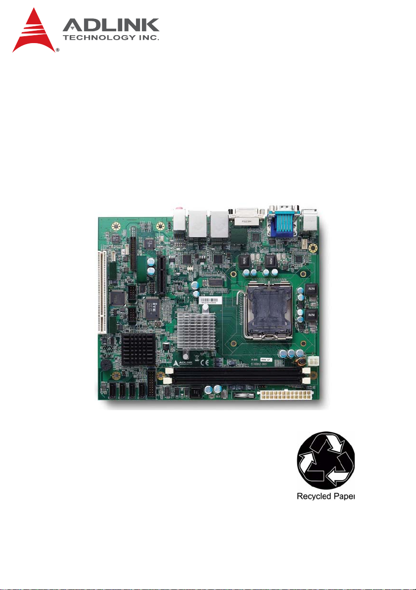
M-321
FlexATX Industrial Motherboard with
Intel® Q45 Chipset
User’s Manual
Manual Rev.: 2.00
Revision Date: May 12, 2010
Part No: 50-1Z032-1000
Advance Technologies; Automate the World.
Page 2

Revision History
Revision Release Date Description of Change(s)
2.00 2010/05/12 Initial Release
Page 3

M-321
Preface
Copyright 2010 ADLINK Technology Inc.
This document contains proprietary infor mation protected by copyright. All rights are reserved. No part of this manual may be reproduced by any mechanical, electronic, or other means in any form
without prior written permission of the manufacturer.
Disclaimer
The information in this document is subject to change without prior
notice in order to improve reliability, design, and function and does
not represent a commitment on the part of the manufa cturer.
In no event will the manufacturer be liable for direct, indirect, special, incidental, or consequential damages arising out of the use or
inability to use the product or documentation, even if advised of
the possibility of such damages.
Environmental Responsibility
ADLINK is committed to fulfill its social responsibility to global
environmental preservation through compliance with the European Union's Restriction of Hazardous Substances (RoHS) directive and Waste Electrical and Electronic Equipment (WEEE)
directive. Environmental protection is a top priority for ADLINK.
We have enforced measures to ensure that our products, manufacturing processes, components, and raw materials have as little
impact on the environment as possible. When products are at their
end of life, our customers are encouraged to dispose of them in
accordance with the product disposal and/or recovery programs
prescribed by their nation or company.
Trademarks
Product names mentioned herein are used for identification purposes only and may be trademarks and/or registered trademarks
of their respective companies.
Preface iii
Page 4

Using this Manual
Audience and Scope
The M-321 User’s Manual is intended for hardware technicians
and systems operators with knowledge of installing, configuring
and operating industrial grade computers.
Manual Organization
This manual is organized as follows:
Preface: Presents copyright notifications, disclaimers, trade-
marks, and associated information on the proper usage of this
document and its associated product(s).
Chapter 1, Introduction: Introduces the M-321, its features,
applications, and specifications, including functional descriptions
and board layout.
Chapter 2, Connectors & Jumpers: Provides technical information on connectors, jumpers and pin assignments for configuring
the M-321.
Chapter 3, Getting Started: Describes how to install components
and drivers on the M-321.
Chapter 4, BIOS Setup: Presents information aid in configuring
the system BIOS.
Appendix A, Watchdog Timer: Presents information on understanding and configuring the watchdog timer.
Appendix B, System Resources: Presents information on I/O
mapping, IRQ routing, and resource allocation.
Important Safety Instructions: Presents safety instructions all
users must follow for the proper setup, installation and usage of
equipment and/or software.
Getting Service: Contact information for ADLINK’s worldwide
offices.
iv Preface
Page 5
M-321
Conventions
Take note of the following conventions used throughout this
manual to make sure that users perform certain tasks and
instructions properly.
Additional information, aids, and tips that help users perform
tasks.
NOTE:
NOTE:
Information to prevent minor physical injury, component damage, data loss, and/or program corruption when trying to com-
CAUTION:
WARNING:
plete a task.
Information to prevent serious physical injury, component
damage, data loss, and/or program corruption when trying to
complete a specific task.
Preface v
Page 6

This page intentionally left blank.
vi Preface
Page 7

M-321
Table of Contents
Revision History...................................................................... ii
Preface.................................................................................... iii
List of Figures........................................................................ xi
List of Tables........................................................................ xiii
1 Introduction ........................................................................ 1
1.1 Package Contents ............................................................... 1
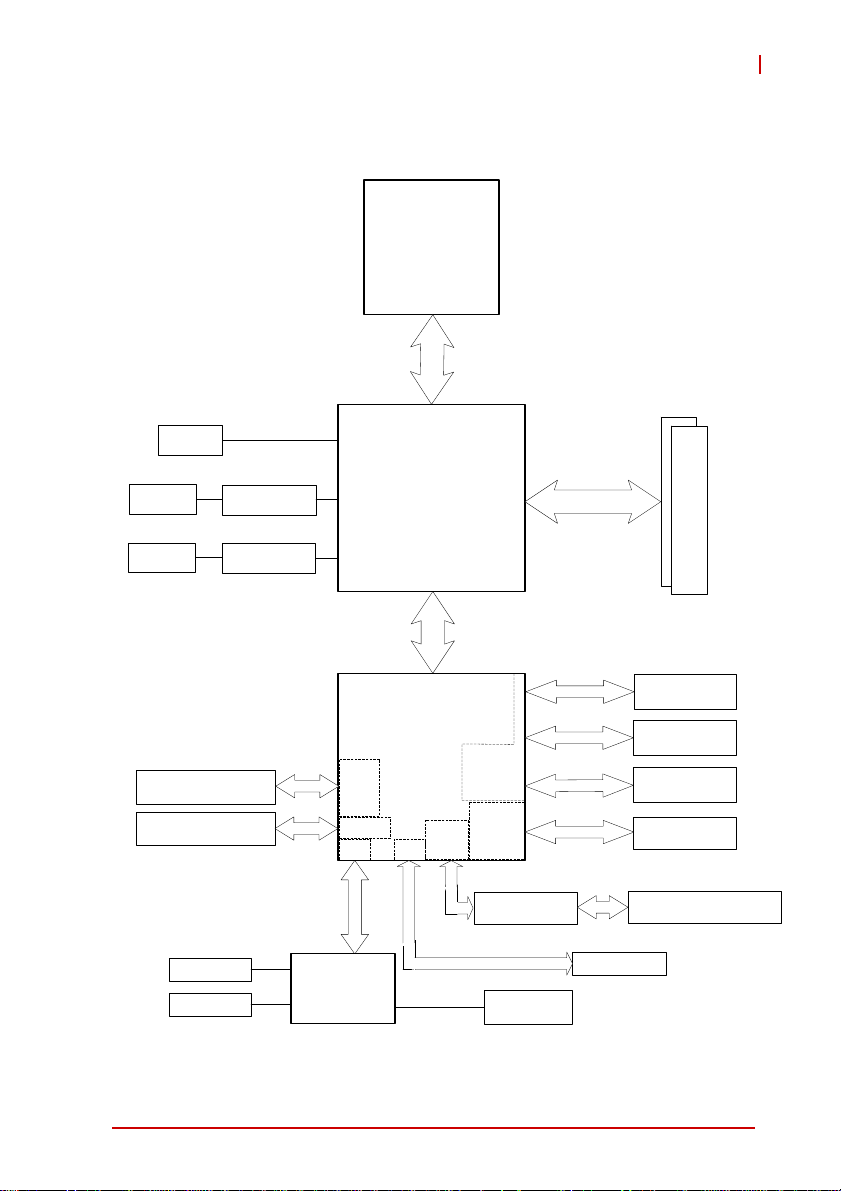
1.2 Overview.............................................................................. 2
1.3 Features............................................................................... 2
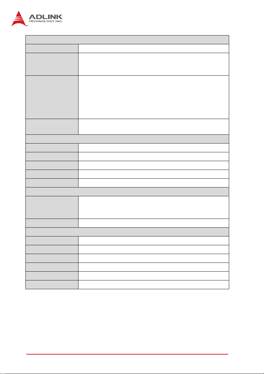
1.4 Specifications....................................................................... 3
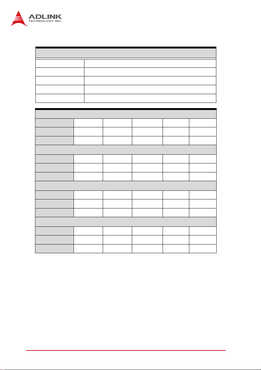
1.5 Power Consumption ............................ ... ... ... ... .... ... ... ... .... ... 5
1.6 Block Diagram ..................................................................... 7
1.7 Functional Description ......................................................... 8
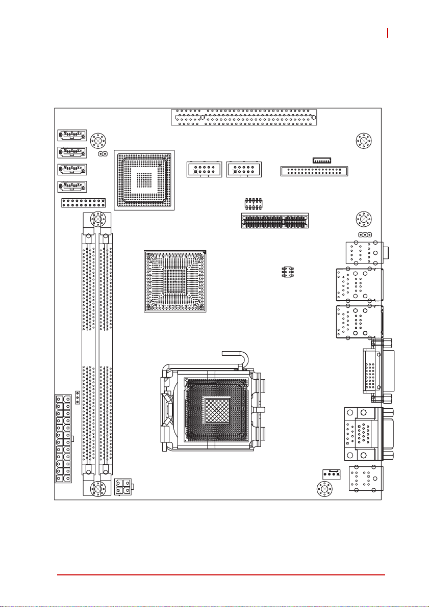
1.8 Board Layout ..................................................................... 11
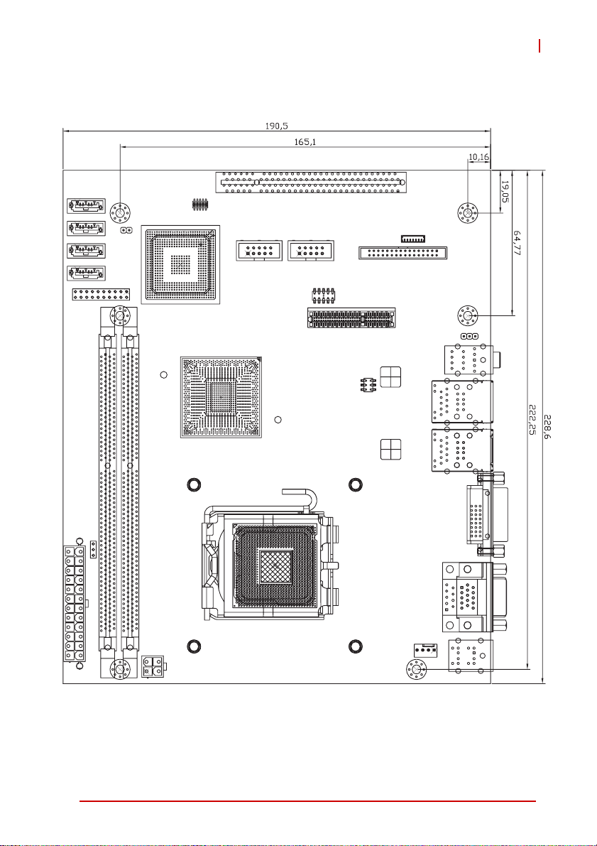
1.9 Mechanical Drawings......................................................... 13
2 Connectors & Jumpers.................................................... 15
2.1 Rear I/O Connectors.......................................................... 15
2.2 Onboard Connectors ......................................................... 19
2.3 Jumpers............................................................................. 25
3 Getting Started ................................................................. 27
3.1 Installing the CPU.............................................................. 27
3.2 Installing the CPU Fan and Heatsink................................. 31
3.3 System Memory................................................................. 33
3.4 Driver Installation................................................. ... ... ... .... . 35
Table of Contents vii
Page 8

4 BIOS Setup........................................................................ 37
4.1 Starting the BIOS............................................................... 37
4.2 Main Setup......................................................................... 41
4.3 Advanced BIOS Setup....................................................... 42
4.3.1 CPU Configuration.........................................................43
4.3.2 IDE Configuration ..........................................................44
4.3.3 Super IO Configuration..................................................45
4.3.4 Hardware Health Configuration .....................................46
4.3.5 Remote Access Configuration .......................................49
4.3.6 USB Configuration.........................................................51
4.3.7 Trusted Computing ........................................................53
4.4 PCI/PnP Settings............................................................... 54
4.4.1 IRQ/DMA .......................................................................54
4.5 Boot Settings ..................................................................... 55
4.5.1 Boot Settings Configuration...........................................55
4.5.2 Boot Device Priority .......................................................57
4.5.3 Boot Device Groups.......................................................57
4.6 Security Setup.................................................................... 58
4.7 Chipset Setup .................................................................... 61
4.7.1 North Bridge Configuration ............................................62
4.7.2 South Bridge Configuration............................................63
4.7.3 Advanced Chipset Settings............................................64
4.8 Exit Menu........................................................................... 65
A Appendix: Watchdog Timer..............................................67
A.1 Sample Code..................................................................... 67
B Appendix: System Resources..........................................71
B.1 System Memory Map......................................................... 71
B.2 Direct Memory Access Channels....................................... 71
B.3 I/O Map................. ... ... .... ... ... ... .... ... ... ................................ 72
B.4 Interrupt Request (IRQ) Lines............................................ 73
viii Table of Contents
Page 9

M-321
B.5 PCI Configuration Space Map ........................................... 76
B.6 PCI Interrupt Routing Map................................................. 78
Important Safety Instructions.............................................. 79
Getting Service...................................................................... 81
Table of Contents ix
Page 10

This page intentionally left blank.
xTable of Contents
Page 11

M-321
List of Figures
Figure 1-1: M-321 Block Diagram ...................................................... 7
Figure 1-2: M-321 Board Layout...................................................... 11
Figure 1-3: M-321 Rear I/O Layout.................................................. 12
Figure 1-4: M-321 Board Dimensions.............................................. 13
List of Figures xi
Page 12

This page intentionally left blank.
xii List of Figures
Page 13

M-321
List of Tables
Table 1-1: M-321 General Specifications..........................................4
Table 1-2: M-321 Board Layout Legend.........................................12
Table 2-1: COM Serial Port Connector Pin Definition..................... 16
Table 2-2: DVI-D Connector Pin Definition..................................... 17
Table B-1: System Memory Map..................................................... 71
Table B-2: Direct Memory Access Channels................................... 71
Table B-3: I/O Map..........................................................................72
Table B-4: IRQ Lines PIC Mode....................... ... ... ... ... .... ... ... ... .... .. 73
Table B-5: IRQ Lines APIC Mode....................... ... ... ... .... ... ...... .... .. 75
Table B-6: PCI Configuration Space Map.... .... ... ... ... ... .... ... ... ... .... .. 77
Table B-7: PCI Interrupt Routing Map.............................. ... ... ... .... .. 78
List of Tables xiii
Page 14

This page intentionally left blank.
xiv List of Tables
Page 15

1 Introduction
This chapter will introduce the M-321, its features, specifications,
functional description, and mechanical layout.
1.1 Package Contents
Please check that your package contains the items below. If
you discover damaged or missing items, please contact your
vendor.
X M-321 Industrial FlexATX Motherboard
X I/O shield
X 2x SATA cable
X 1x dual-plug SATA power cable
X 1x COM port cable with bracket
X Driver DVD
X User’s Manual
M-321
DO NOT install or apply power to equipment that is damaged
or if there is missing/incomplete equipment. Retain the ship-
WARNING:
Introduction 1
ping carton and packing materials for inspection. Please contact your ADLINK dealer/vendor immediately for assistance.
Obtain authorization from your dealer before returning any
product to ADLINK.
Page 16

1.2 Overview
The ADLINK M-321 is a FlexATX industrial motherboard supporting the next-generation Intel® Core™2 Quad/Duo, Pentium® Dual
Core and Celeron® processors in the LGA775 package to deliver
a high performance platform for a wide array of industrial applications. The M-321 supports 45nm process CPUs at up to 3.00GHz
and 1333 MHz Front Side Bus (FSB). Dual channel DDR3
800/1066 MHz memory is supported up to a maximum of 4GB in
two DIMM slots. The M-321 supports a broad range of processor
frequencies, high-speed data transfer rates, diverse I/O functions,
and high-bandwidth network connectivity.
These advanced features, coupled with a dual-channel DDR3 system memory architecture, integrated graphics supporting
VGA/DVI/LVDS, one PCI Express® x4, one PCI slot, and audio
interfaces make the M-321 suitable for automation control, medical, test & measurement, and telecom applications requiring an
easy-to-deploy and reliable mainboard.
1.3 Features
X FlexATX form factor (229 mm x 191 mm)
X Supports Intel® Core™2 Quad/Duo, Pentium® Dual Core
and Celeron® processors in LGA775 package
X Dual 10/100/1000Mbps Ethernet
X 8x USB 2.0 ports (4x faceplate, 4x onboard pin header)
X 4x SATA 3 Gbps ports
X Integrated graphic supports VGA, DVI, LVDS
X One PCI Express® x4 and one PCI slot
X Watchdog Timer, Hardware Moni tor
X Realtek ALC262 HD audio codec
X TPM hardware security chip
X RoHS compliant
2Introduction
Page 17

M-321
1.4 Specifications
System
CPU/Cache • IIntel® Core™2 Quad Q9400, 2.66GHz, 1333MHz FSB,
6MB L2 Cache, 45nm
• Intel® Core™2 Duo E8400, 3.0GHz, 1333MHz FSB,
6MB L2 Cache, 45nm
• Intel® Core™2 Duo E7400, 2.8GHz, 1066MHz FSB,
3MB L2 Cache, 45nm
• Intel® Core™2 Duo E6400, 2.13GHz, 1066MHz FSB,
2MB L2 Cache, 65nm
• Intel® Pentium® Dual Core E5300, 2.6GHz, 800MHz FSB,
2MB L2 Cache, 45nm
• Intel® Core™2 Duo E4300, 1.8GHz, 800MHz FSB,
2MB L2 Cache, 65nm
• Intel® Pentium® Dual Core E2160, 1.8GHz, 800MHz FSB,
1MB L2 Cache, 65nm
• Intel® Celeron® 440, 2.0GHz, 800MHz FSB,
512KB L2 Cache, 65nm
FSB • 800/1066/1333 MHz
Chipset • Intel® 82Q45 Graphics Memory Controller Hub
• Intel® ICH10 I/O Controller Hub
Memory • Two 240-pin DIMM sockets support 800/1066MHz
DDR3 (up to 4GB)
BIOS • AMI BIOS with 8 Mb Flash ROM
TPM • Infneon® SLB9635 TT1.2
Audio • Realtek ALC262 HD codec
• Supports line-in, line-out and mic-in
Watchdog Timer • 1-255 second/minute programmable
Hardware Monitor • CPU/System temperature, fan speed and onboard DC
voltage
Operating System • Windows® XP/Vista
• Windows® Vista 64-bit
• Fedora™ 10
Introduction 3
Page 18
I/O Interfaces
Serial ATA • 4x Serial ATA ports with 300 MB/s data transfer
Onboard I/O • 2x USB 2.0 pin headers (4 ports)
• 1x RS-232 serial po rt connector
• 1x front panel pin header
Rear I/O • 2x RJ-45 LAN port
• 4x USB 2.0 ports
• 1x D-Sub VGA connector
• 1x DVI-D connector
• 2x PS2 keyboard/mouse ports
• 3x audio jacks (line-in, line-out and mic-in)
Expansion Slots • 1x PCIe x4 slot
•1x PCI slot
Display
VGA • GMA 4500 integrated in Q45 GMCH
VRAM • Shared system memory up to 512 MB
CRT • Dsub-15 connector, up to 2048x1536 @ 75 Hz
DVI • DVI-D interface, resolution up to UXGA (1600 x 1200)
LVDS • Single channel 24-bit LVDS
Ethernet
Controller • Dual Intel® 82574L PCIe network controllers
• 10/100/1000Base-T dual-Gigabit Ethernet
• Wake on LAN supported
Ports • 2x RJ-45 Ethernet port
Mechanical and Environment
Form Factor • FlexATX Industrial Motherboard
Dimensions • 229 mm x 191 mm (L x W)
Operating Temp. • 0°C to 60°C
Storage Temp. • -20ºC to 80ºC
Rel. Humidity • 10 - 90% RH
Safety • CE, FCC Class A
T able 1-1: M-321 General Specifications
4Introduction
Page 19

M-321
1.5 Power Consumption
Intel® Core™2 Quad Processor Q9400
T est Configuration
CPU Intel® Core™2 Quad Processor Q9400 2.66 GHz
Memory Transcend 1GB DDR3 1066DIMM CL7 x2
Graphics Intel ® 82Q45 Graphics Memory controller
SATA Channel 1 Seagate ST3160815AS Barracuda 7200.10 160GB
Power Supply MSI AL-B450E 450W
DOS (idle)
Power Req. +5V +12V CPU +12V +3.3V Total
Current (A) 0.768 0.805 1.714 1.298 —
Watts (W) ————38.35
Windows XP, Idle
Power Req. +5V +12V CPU +12V +3.3V Total
Current (A) 0.703 0.777 0.667 1.319 —
Watts (W) — — — — 25.20
Windows XP, KPower
Power Req. +5V +12V CPU +12V +3.3V Total
Current (A) 0.705 0.918 5.011 1.322 —
Watts (W) — — — — 79.04
Windows XP, BurnIn Test 6.0
Power Req. +5V +12V CPU +12V +3.3V Total
Current (A) 0.878 0.968 3.570 1.324 —
Watts (W) ————63.21
Introduction 5
Page 20
Intel® Core™2 Duo Processor E8400
T e st Con f ig uration
CPU Intel® Core™2 Duo Processor E8400 3.00 GHz
Memory Transcend 1GB DDR3 1066DIMM CL7 x2
Graphics Intel ® 82Q45 Graphics Memory controller
SATA Channel 1 Seagate ST3160815AS Barracuda 7200.10 160GB
Power Supply MSI AL-B450E 45 0W
DOS (idle)
Power Req. +5V +12V CPU +12V +3.3V Total
Current (A) 0.756 0.873 2.906 1.283 —
Watts (W) — — — — 53.36
Windows XP, Idle
Power Req. +5V +12V CPU +12V +3.3V Total
Current (A) 0.704 0.798 0.826 1.297 —
Watts (W) — — — — 27.29
Windows XP, KPower
Power Req. +5V +12V CPU +12V +3.3V Total
Current (A) 0.709 0.950 4.651 1.303 —
Watts (W) — — — — 75.06
Windows XP, BurnIn Test 6.0
Power Req. +5V +12V CPU +12V +3.3V Total
Current (A) 0.830 1.013 4.037 1.303 —
Watts (W) — — — — 69.05
6Introduction
Page 21
1.6 Block Diagram
CPU
Intel® Celeron/
Core™ 2
Duo/Quad
800/1066/1333 MHz FSB
LGA775 Socket
800/1066/1333 MHz FSB
M-321
CRT
DB-15
LVDS
DVI
Chrontel 7308B
LVDS Transmitter
Chrontel 7318C
DVI Transmitter
SATA ports x4
USB 2.0
(Bracket x4, Internal x4)
KB/Mouse
RS-232 x2
Northbridge
Intel®Q45 GMCH
Southbridge
Intel® ICH10
SATA
USB 2.0
LPC
SPI
ITE
IT8718F
LPC Super I/O
AC97
DMI
Interface
2 GB/s
PCIe
Controller
PCI
Controller
Realtek ALC262
Audio Codec
Hardware
Monitor
DDR3 800/1066MHz
PCIe x4 PCIe x4 slot
Intel
PCIe x1
I
e
P
C
PCI Bus
x
1
82574L
RJ-45
Intel
82574L
RJ-45
PCI 32-bit/
33MHz bus
Audio Jacks
Line-in, Line-out, Mic-in
SPI BIOS
DDR3 DIMMs up to 4GB
Figure 1-1: M-321 Block Diagram
Introduction 7
Page 22

1.7 Functional Description
Processor Support
The M-321 is a single processor design for the latest Intel Yorkfield/Wolfdale/Conroe Processor family, starting from 1.8 GHz
core frequency up to 3.0 GHz. With one LGA775 socket, the CPU
connects with the Intel® Q45 MCH through the
800/1066/1333 MHz Front Side Bus (FSB).
Intel® Q45 + ICH10 Express Chipset
The Intel® Q45 Express chipset provides the vital interfaces for
the SHB. The Intel® Q45 comes with purpose-built capabilities
designed specifically to address the key needs of the industrial
computing environment and delivers improved system performance and comes with the integrated Intel® Graphics Media
Accelerator 4500 engine for cost-effective system building. The
chipset also supports high-bandwidth interfaces including PCI
Express, Serial ATA, and USB 2.0, as well as dual-channel DDR3
system memory.
Intel® Graphics Media Accelerator 4500
The Intel® Graphics Media Accelerator (GMA) 4500 r evolutionizes
integrated graphics with new capabilities that provide significant
increase in graphics performance. With support for DirectX 10
hardware acceleration, Shader Model 4.0 and OpenGL 2.0, the
Intel GMA 4500 delivers excellent video and 3D graphics for a
cost-effective and high-performance graphics solution.
Dual-Channel DDR3 Memory
To meet the requirements of memory-intensive applications, the
M-321 has a dual-channel memory architecture supporting DDR3
800/1066 MHz DIMMs. The key advantages of DDR3 are the
higher bandwidth and the increase in performance at lower power
than DDR2. DDR3 memory technology meets the requirements of
the latest 3D graphics, multimedia, and network application, and
boosts system performance by eliminating bottlenecks.
8Introduction
Page 23

M-321
Gigabit Ethernet
The M-321 uses two Intel® 82574L Gigabit Ethernet controllers
connected to the PCI-E x1 bus of the ICH10. Operation at data
rates of 10/100/1000 Mbps, wake on LAN and PXE are supported.
Serial ATA Technology
Storage is efficient and secure with the Serial ATA interface. Utilizing the Intel® ICH10, the M-321 supports up to four Serial ATA
devices capable of reading/writing data at up to 3 Gbps. The
SATA specification improves chassis airflow via thinner and more
flexible cables with lower pin count.
Universal Serial Bus 2.0
The M-321 incorporates the Universal Serial Bus (USB) 2.0 specification that increases peripheral connection speed from 12 Mbps
(USB 1.1) to 480 Mbps.
Hardware Monitoring
A built-in, proactive hardware monitoring system monitors the
CPU temperature, system fan rotations, and voltage levels to prevent overheating and/or component damage, effect timely failure
detection, and ensure stable supply of current for critical components.
Watchdog Timer
The watchdog timer (WDT) monitors system operations based on
user-defined configurations. The WDT can be programmed for different time-out periods, such as from 1 to 255 seconds or from 1 to
255 minutes. The WDT generates a reset signal, then a reset
request, after failure to strobe it within the programmed time
period. A register bit may be enabled to indicate if the watchdog
timer caused the reset event. The WDT register is cleared during
the power-on sequence to enable the operating system to take
appropriate action when the watchdog generates a reboot.
Introduction 9
Page 24

Trusted Platform Module
The M-321 supports TPM ver. 1.2 (Trusted Platform Module) for
secure storage of keys, passwords and digital certificates. Systems supporting TPM offer improved hardware-based security in
numerous applications, such as file and folder encryption, local
password management, S-MIME e-mail, VPN and PKI authentication and wireless authentication for 802.1x and LEAP.
10 Introduction
Page 25
1.8 Board Layout
M-321
SLOT1
CN11/13/14/16
CN22
DIMM2
JP3
CN23
JP1
DIMM1
CN15 CN12
CN20
CN5
CN6
PCIE1
JP4
CN19
FAN1
CN24
Figure 1-2: M-321 Board Layout
Introduction 11
Page 26
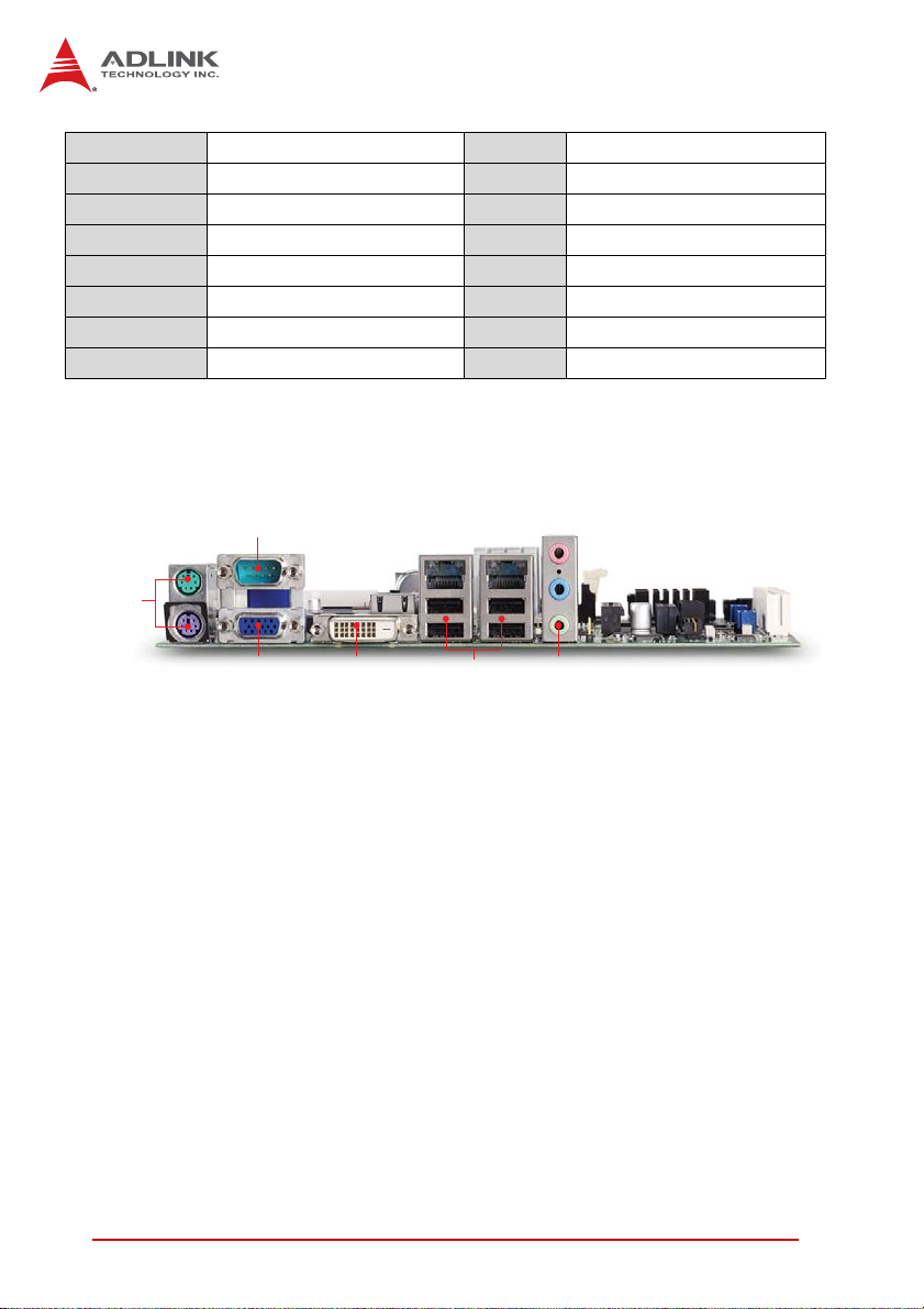
CN5 L VDS Inverter connector CN24 ATX12V power connector
CN6 LVDS connector FAN1 CPU Fan connector
CN11/13/14/16 SATA connectors DIMM1/2 Memory slots
CN12/15 USB pin headers JP1 Chassis Intrusion pin header
CN19 LAN LED pin header JP3 Clear CMOS jumper
CN20 COM2 connector JP4 Audio Line-Out pin Header
CN22 System Panel connector PCIE1 PCIe x4 slot
CN23 ATX power connector Slot1 PCI slot
Table 1-2: M-321 Board Layout Legend
COM
PS/2
KB/MS
VGA DVI
Figure 1-3: M-321 Rear I/O Layout
12 Introduction
RJ-45 + USB
Audio
Page 27
1.9 Mechanical Drawings
M-321
Dimensions in mm
Figure 1-4: M-321 Board Dimensions
Introduction 13
Page 28

This page intentionally left blank.
14 Introduction
Page 29
2 Connectors & Jumpers
The connectors and jumpers on the M-321 allow you to connect
and configure external devices. The following specify the pin
assignments for connectors and jumper on the M-321. Refer to
Figure 1-2: M-321 Board Layout and Figure 1-3: M-321 Rear
I/O Layout for connector and jumper locations.
2.1 Rear I/O Connectors
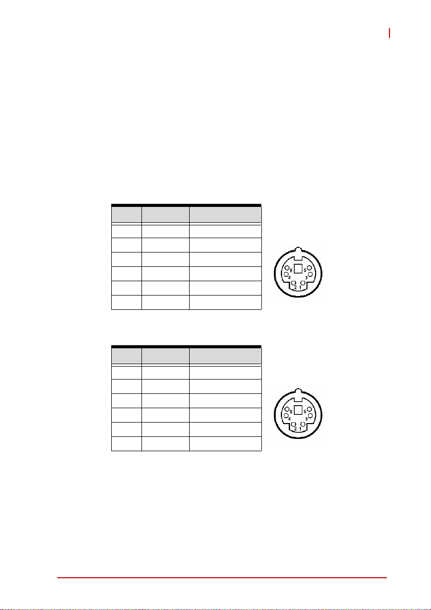
PS/2 Mouse Port (green)
Pin # Signal Function
1MSDATAMouse Data
2 NC not connected
3 GND Ground
4+5V Power
5 CLK Clock
6 NC not connected
M-321
PS/2 Keyboard Port (purple)
Pin # Signal Function
1 KBDATA Keyboard Data
2 NC not connected
3 GND Ground
4+5V Power
5 CLK Clock
6 NC not connected
Connectors & Jumpers 15
Page 30
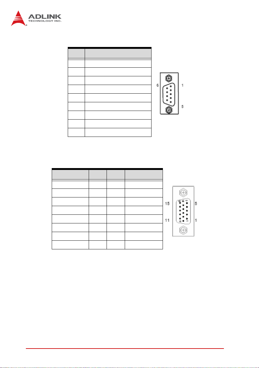
COM DB-9 Serial Port Connector
Pin # RS-232
1 DCD, Data carrier detect
2 RXD, Receive data
3 TXD, Transmit data
4 DTR, Data terminal ready
5 IsoGND, Isolated ground
6 DSR, Data set ready
7 RTS, Request to send
8 CTS, Clear to send
9 RI, Ring indicator
Table 2-1: COM Serial Port Connector Pin Definition
VGA Connector.
Signal Name Pin # Pin # Signal Name
Red 1 2 Green
Blue 3 4 VCC pull-up
GND 5 6 GND
GND 7 8 GND
VCC 9 10 GND
VCC pull-up 11 12 DDC2B DATA
HSYNC 13 14 VSYNC
DDC2B CLK 15
16 Connectors & Jumpers
Page 31
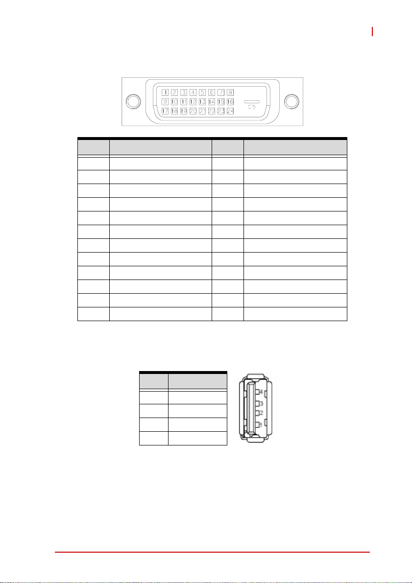
DVI-D Connector)
Pin # Signal Pin # Signal
1 TMDS Data2- 13 TMDS Data3+
2 TMDS Data2+ 14 +5 V Power
3 TMDS Data2/4 Shield 15 GND
4 TMDS Data4- 16 Hot Plug Detect
5 TMDS Data4+ 17 TMDS Data06 DDC Clock [SCL] 18 TMDSData0+
7 DDC Data [SDA] 19 TMDS Data0/5 Shield
8 Analog vertical sync 20 TMDS Data5-
9 TMDS Data1- 21 TMDS Data5+
10 TMDS Data1+ 22 TMDS Clock Shield
11 TMDS Data1/3 Shield 23 TMDS Clock +
12 TMDS Data3- 24 TMDS Clock -
M-321
Table 2-2: DVI-D Connector Pin Definition
USB Connectors
Pin # Signal Name
1Vcc
2 USB3 USB+
4GND
Connectors & Jumpers 17
Page 32
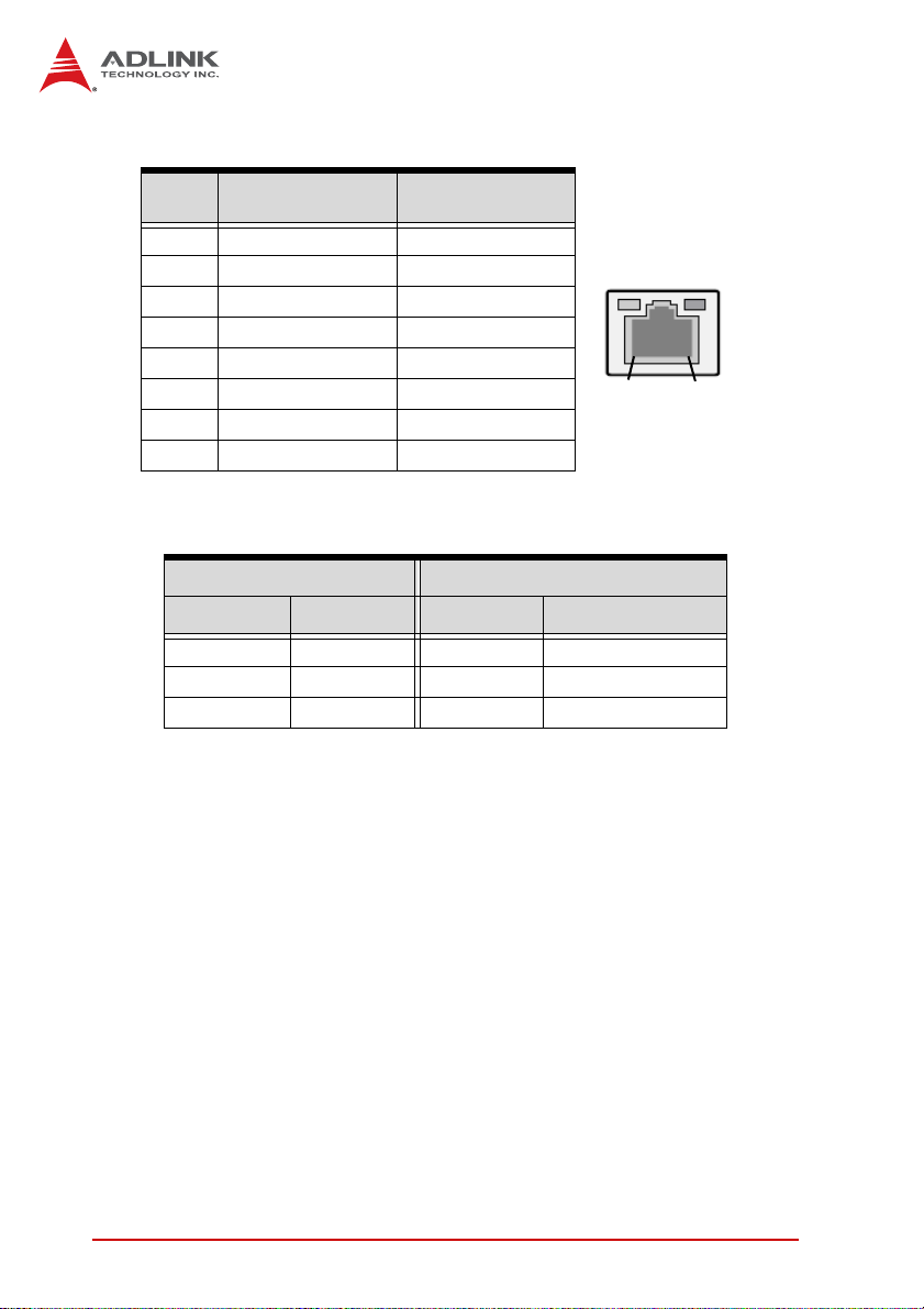
LAN (RJ-45) Ports
Pin #
1 TX+ BI_DA+
2 TX- BI_DA3 RX+ BI_DB+
4 -- BI_DC+
5-- BI_DC6 RX- BI_DB7 -- BI_DD+
8-- BI_DD-
10BASE-T/
100BASE-TX
1000BASE-T
LED1
LED2
18
Refer to the table below for the LAN port LED definitions.
LED1 LED2
Status Description Status Description
Off No Link Off 10 Mb connection
On Linked Green 100 Mb connection
Blinking Data Activity Amber 1 Gb connection
Audio I/O port
The three-jack audio I/O supports Line-In, Line-Out, and Mic-In
functions. The blue Line-In jack onnects to an audio source such
as a CD player. The green Line-Out port connects to a speaker or
headphone, while the pink Mic-In jack connects to a microphone.
18 Connectors & Jumpers
Page 33
2.2 Onboard Connectors
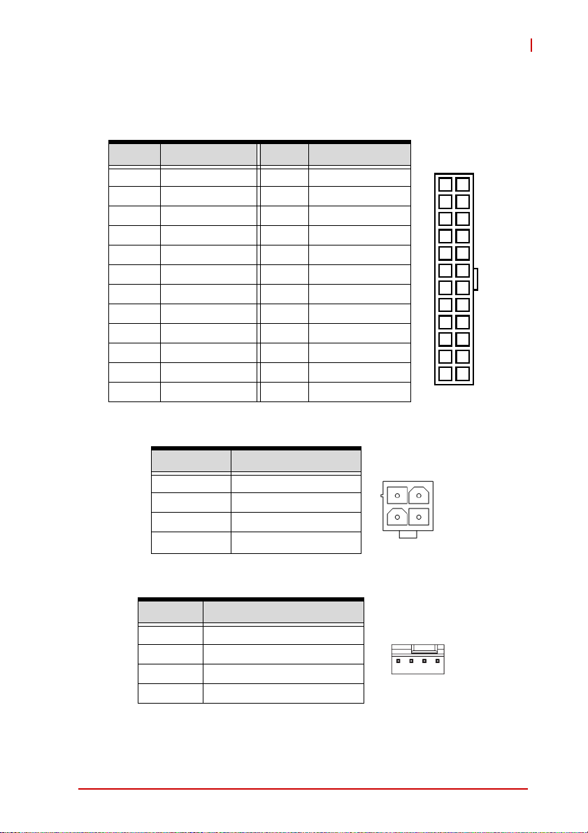
ATX Power Connector (CN23)
Pin # Signal Pin # Signal
1 +3.3V 13 +3.3V
2 +3.3V 14 -12V
3 GND 15 GND
4 +5V 16 PS-ON#
5 GND 17 GND
6 +5V 18 GND
7 GND 19 GND
8 PWRGD 20 NC
9 +5VSB 21 +5V
10 +12V 22 +5V
11 +12V 23 +5V
12 24-pin detection 24 GND
ATX 12V Power Connector (CN24)
12
M-321
24
1
13
Pin # Signal
1 GND
2 GND
3 +12V DC
4 +12V DC
2
4
1
3
CPU Fan Connector (CPU_FAN)
Pin # Signal
1 GND
2 VCC
3 FAN_SENSE
4 FAN_CONTROL
Connectors & Jumpers 19
14
Page 34
13 14
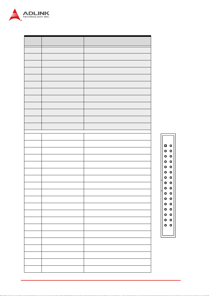
LVDS Connector (CN6)
Pin # Signal Name Signal Description
1 CLK2M Channel B clock port output 2 CLK2P Channel B clock port output +
3 SHGND Shield GND
4 B3M Channel B data port output 5 B3P Channel B data port output +
6 B2M Channel B data port output 7 B2P Channel B data port output +
8 SHGND Shield GND
9 B1M Channel B data port output 10 B1P Channel B data port output +
11 B0M Channel B data port output 12 B0P Channel B data port output +
13 SHGND Shiel d GND
14 A3M Channel A data port output 15 A3P Channel A data port output +
16 SHGND Shiel d GND
17 CLK1M Channel A clock port output 18 CLK1P Channel A clock port output +
19 SHGND Shiel d GND
20 A2M Channel A data port output 21 A2P Channel A data port output +
22 SHGND Shiel d GND
23 A1M Channel A data port output 24 A1P Channel A data port output +
25 SHGND Shiel d GND
26 A0M Channel A data port output 27 A0P Channel A data port output +
28 Reserved
29 Reserved
30 DDC_SCL Disp Data Channel Clock
31 D DC_SDA Disp Data Channel Data
32 DDC_PWR Disp Data Channel power
20 Connectors & Jumpers
Page 35

Pin # Signal Name Signal Descript ion
33 VSS Return GND
34 VSS Return GND
35 VDD 3.3V FPD VDD power
36 VDD 3.3V FPD VDD power
37 VDD 3.3V FPD VDD power
38 INV_EN Inverter Enable output
10~3V / 0~50k. Brightness
39 INV_V/R_Bright
Output
(set via resistor selection)
40 INV_Rbrightness
0~50k Brightness Output
(set via resistor selection)
41 VEE Return GND
42 VEE Return GND
43 VCC_10.8~13.2V Inverter Power
44 VCC_10.8~13.2V Inverter Power
The standard 32-pin connector consists of pins 13 to 44. Pins
1-12 are reserved for future use with a 42-pin connector to pro-
NOTE:
NOTE:
vide dual channel LVDS support.
M-321
LVDS Inverter Connector (CN5)
Pin # Signal
1 VCC_BKL
2 VCC_BKL
3 GND
4 GND
5 INV_EN
6 INV_BRI1
7 INV_BRI2
Connectors & Jumpers 21
1
Page 36
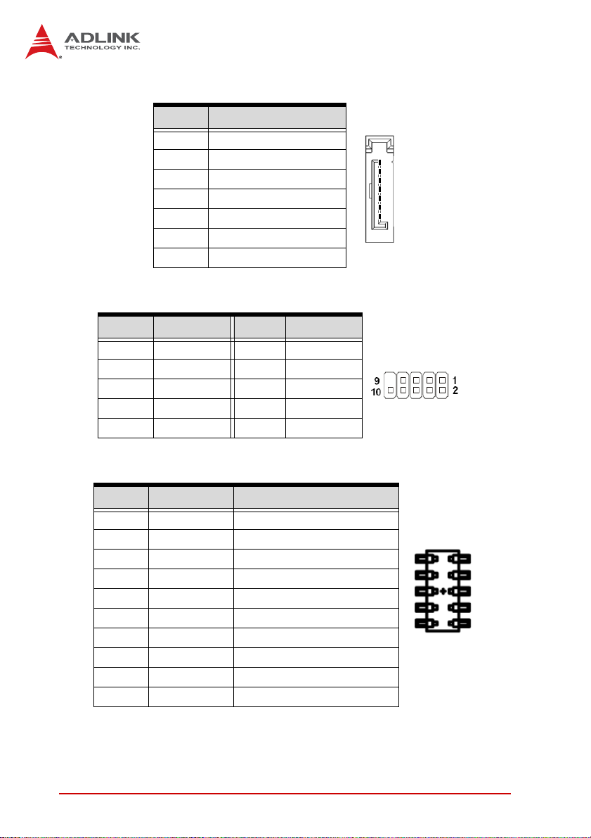
SATA Connectors (CN11/13/14/16)
Pin # Signal
1 GND
2 TXP
3 TXN
4 GND
5 RXN
6 RXP
7 GND
USB Pin Headers (CN12/15)
Pin # Signal Pin # Signal
1+5V 2+5V
3 USB0- 4 USB15 USB0+ 6 USB1+
7 GND 8 GND
9 Key 10 NC
COM2 Connector (CN20)
1
1
7
Pin # Signal Functions
1 DCD Data Carrier Detect
2 TXD Transmit Data
3 GND Ground
1
4 RTS Reque st to Send
5 RI Ring Indicate
6 RXD Receive Data
5
7 DTR Data Terminal Ready
8 DSR Data Set Ready
9 CTS Clear to Send
10 NC Not Connect
22 Connectors & Jumpers
Page 37
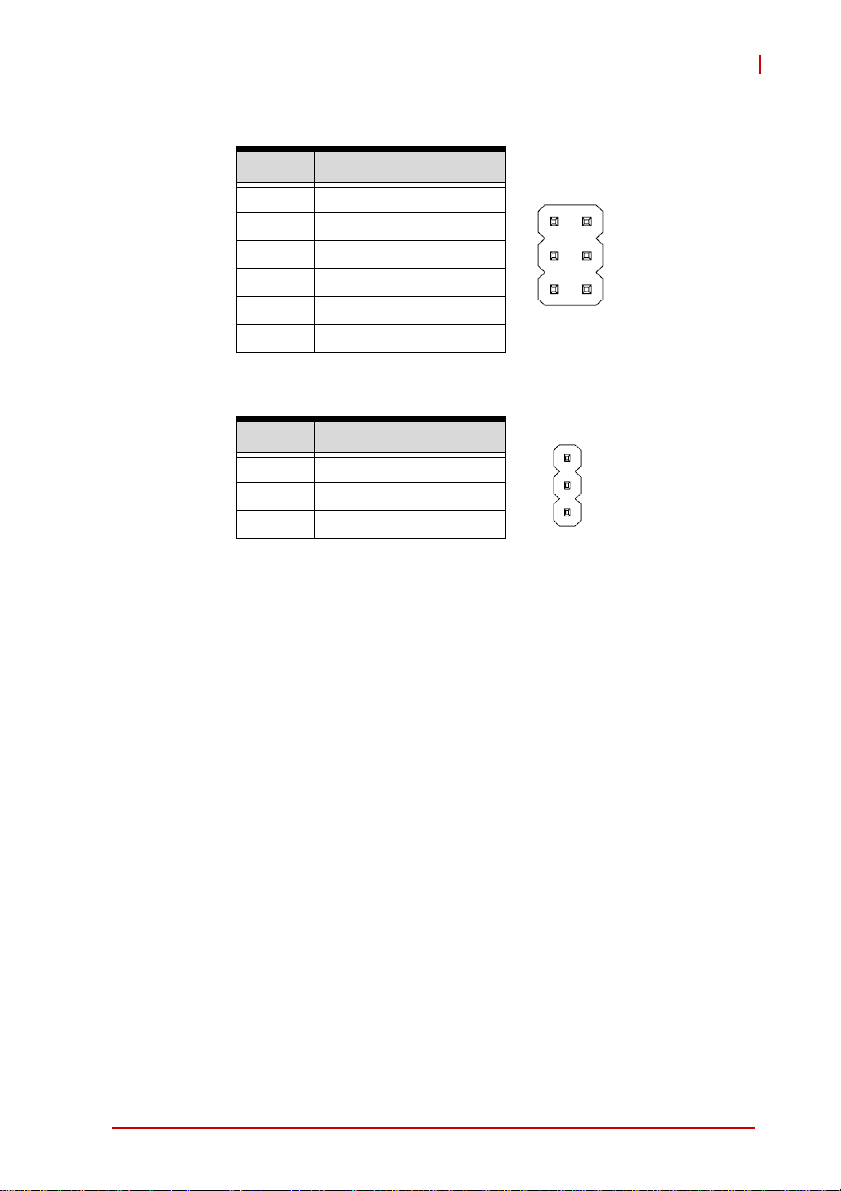
LAN LED Pin Header (CN19)
Pin # Signal
1 ACTLEDP
2 NIN_ACTLED#
3 NIN_LINKLED1#
4 R_NIN_LINKLED2#
5 R_NIN_LINKLED2#
NIN_LINKLED1#
Audio Line-Out Pine Header (JP4)
Pin # Signal
1 LINE-OUT-L
2 GND
3 LINE-OUT-R
M-321
1
5
1
3
Connectors & Jumpers 23
Page 38
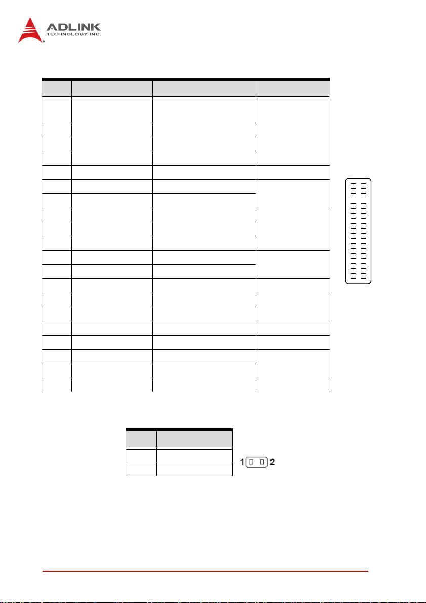
System Panel Connector (CN22)
Pin # Signal Function Pin Group
1
WDSPK/
MONO_OUT
2 HEADPHONE-L Audio signal
3 AGND
4 P5V Power
5 HEADPHONE-R Audio signal
6 GND Ground
7 KEYLOCK Keyboard lock
8 PLED Power LED signal
10 P5V Power LED pull-up
11 GND Ground
12 RESETBT RESET signal
13 NC
14 GND Ground
15 POWERBT Power-on signal
16 NC
17 NC
18 HDDLED Hard Disk LED signal
19 P3V3 Hard Disk LED pull-up
20 NC
Speaker signal/
Audio signal
Chassis
Speaker
Key Lock
Power LED9 HEADPHONE-JD Audio sense
RESET button
Power on button
Hard Disk LED
1
10
11
20
Chassis Intrusion Connector (JP1)
Pin # Signal Name
1INTRUSION
2GND
24 Connectors & Jumpers
Page 39
M-321
2.3 Jumpers
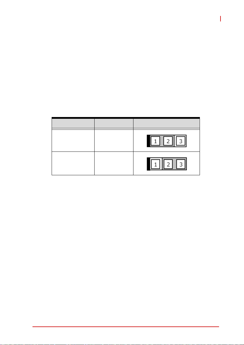
Clear CMOS Jumper (JP3)
The CMOS RAM data contains the date / time and BIOS setting
information. CMOS is powered by the onboard button cell battery.
To erase the CMOS RAM data:
1. Unplug the M-321
2. Short the JP3 pins 2-3
3. Turn the power on. After power on, remove the jumper
cap from pins 2-3 and reinstall it to pins 1-2.
RTC status Connection CLRTC
Normal 1 – 2
Clear CMOS 2 – 3
Connectors & Jumpers 25
Page 40

This page intentionally left blank.
26 Connectors & Jumpers
Page 41
3 Getting Started
This chapter provides information on how to install components to
the M-321 motherboard.
3.1 Installing the CPU
The M-321 Supports the Intel® Core™2 Duo/Quad, Intel® Pentium® Dual-Core, and Intel® Celeron® processors via the surface
mount LGA775 socket (Socket T).
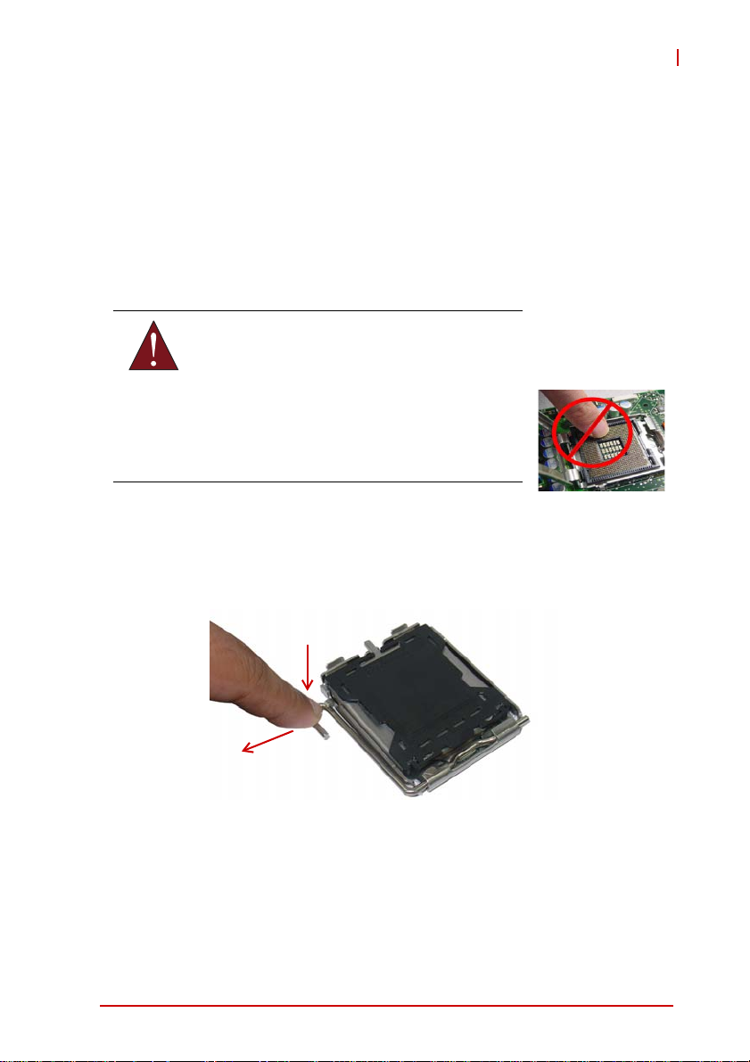
Disconnect all power supply to the board
before installing a CPU to prevent damaging
WARNING:
To install the CPU:
the board and CPU.
Do not touch socket contacts. Damaging the
contacts voids the product warranty. Follow
the installation instructions carefully to avoid
damaging to motherboard components.
1. Press the load lever (A), then disengage it from the
retention tab (B).
M-321
A
B
Getting Started 27
Page 42
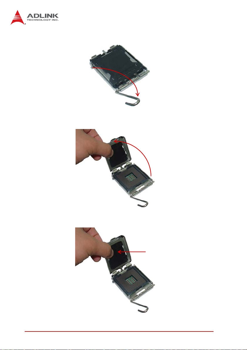
2. Lift and rotate the load lever to a 135° angle
3. Lift the load plate to a 100° angle using your thumb and
forefinger
4. Use your thumb to push and remove the protective
socket cover (plastic) from the load plate
28 Getting Started
Page 43
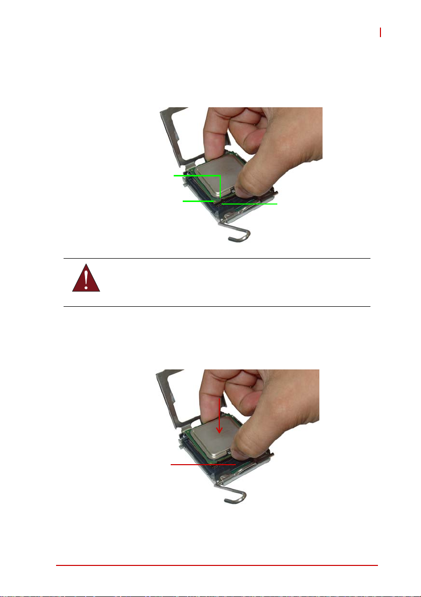
5. Position the CPU over the socket, then match the
notches on the CPU side with the alignment keys on the
socket. The golden triangle on the CPU must be positioned on the bottom-left corner of the socket .
Notch
M-321
Golden triangle
The CPU fits the socket in only one orientation. DO NOT force it
into the socket to avoid damaging it.
WARNING:
Alignment
key
6. Carefully place the CPU on the socket in a vertical
motion. The socket has tabs that accommodate your fingers during installation .
Socket tab
Getting Started 29
Page 44
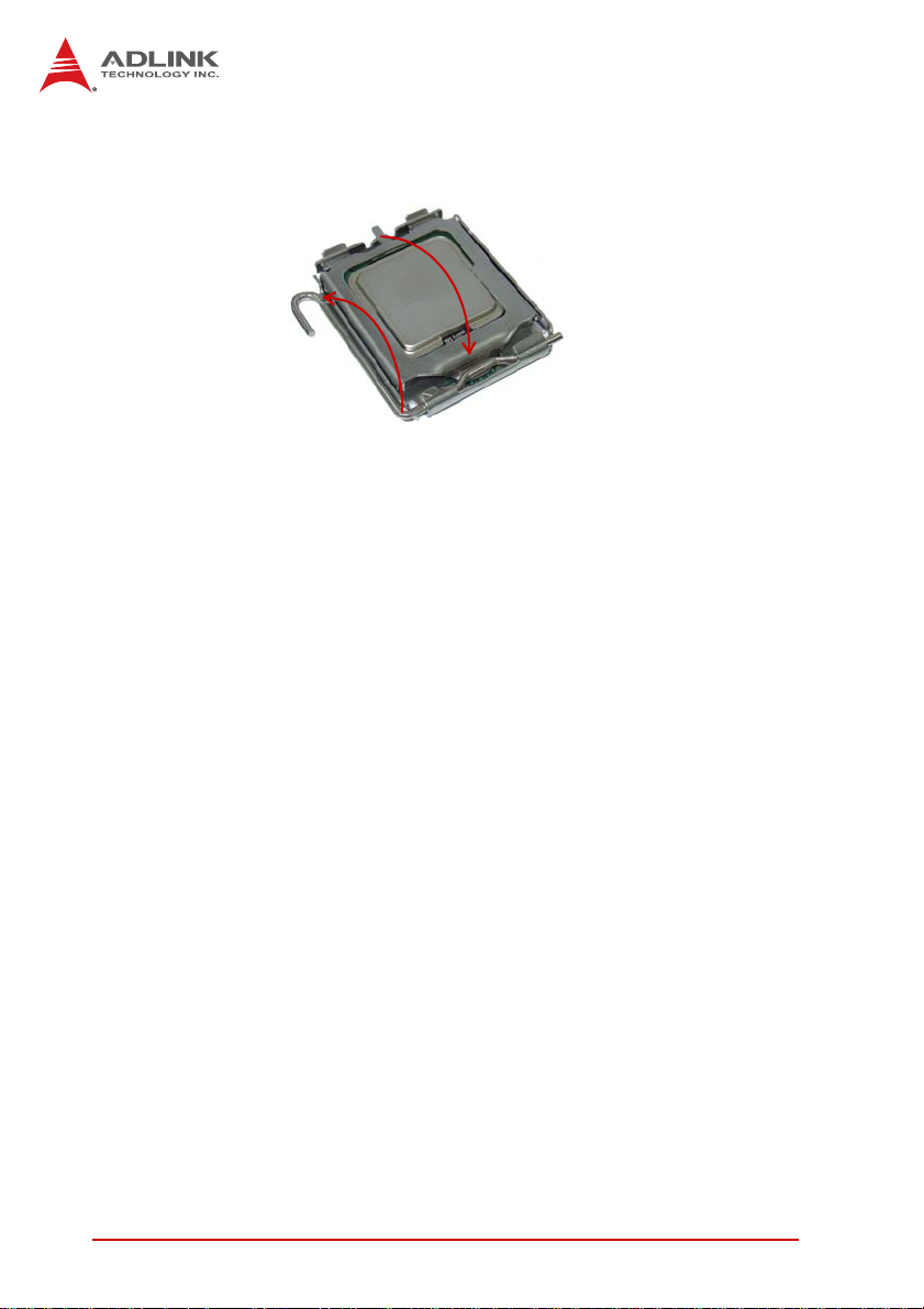
7. Close the load plate (A), then fasten the load lever on
the retention tab (B) .
A
B
30 Getting Started
Page 45
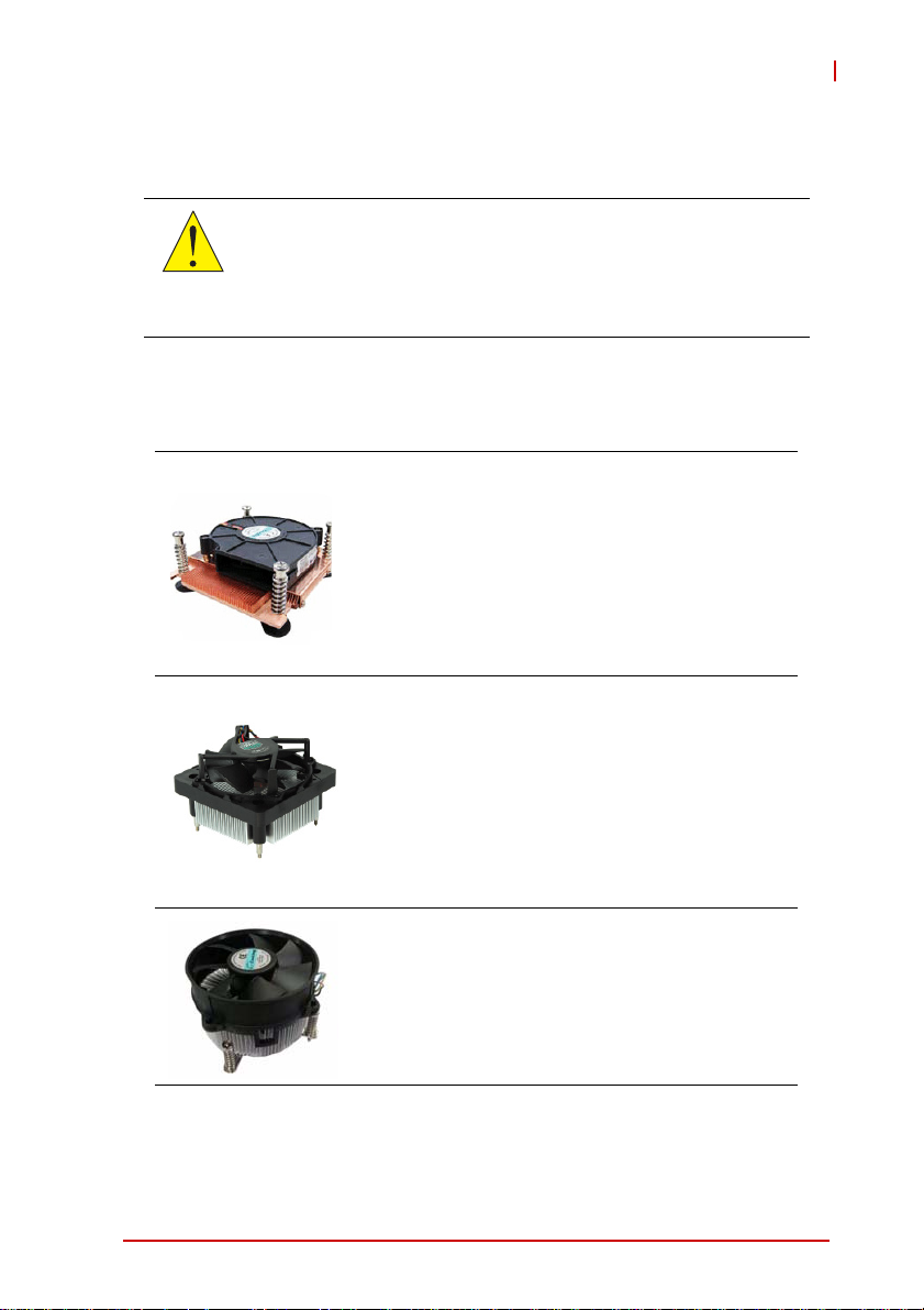
M-321
3.2 Installing the CPU Fan and Heatsink
The CPU requires a chassis with an airflow inlet and maximum
internal ambient temperature of 60° C. A specially-designed
CAUTION:
The following CPU fan and heatsink assemblies are recommended for use with the M-321:
CPU fan and heatsink must be installed before using the motherboard. Failure to install a CPU fan and heatsink may damage
the motherboard and/or the CPU.
1U LGA 775 CPU Cooler
Dimensions:
• Heatsink: 92 x 87.6 x 28 mm
• Fan: 75 x 75 x 15 mm
Heatsink: Copper base + copper skived fin
Fan speed: 5500 RPM
Fan airflow: 10.48 CFM
Noise level: 51 dBA
Part number: 32-20065-0000
3U LGA 775 CPU Cooler
Dimensions:
• Heatsink: 100 x 100 x 70 mm
• Fan: 90 x 90 x 25 mm
Heatsink: Aluminum extrusion
Fan speed: 4500 RPM
Fan airflow: 57.7 CFM
Noise level: 47.5 dBA
Part number: 32-20058-0000 + 34-30381-0000
Copper-Core Cooler
Dimensions: 115 x 115 x 61.4 mm
Heatsink: Aluminum extrusion+copper core
Fan speed: 4500 RPM
Fan airflow: 76.9 CFM
Noise level: 49 dBA
Part number: 32-20086-0000
Getting Started 31
Page 46

When the CPU fan installation procedures presented here are
inconsistent with the installation procedures you obtained from the
CPU fan and heatsink package, follow the latter.
To install the CPU fan:
1. Apply thermal gr ease evenly on top of the in stalled CPU.
2. Lower the CPU fan to the CPU, then secure it using the
provided attachments or screws.
Connect the CPU fan cable to the CPU fan connector on the
motherboard labeled FAN1 (see Figure 1-2 on page 11).
32 Getting Started
Page 47

M-321
3.3 System Memory
The M-321 supports up to 4 GB of DDR3 800/1066 MHz memory
modules via two DDR3 DIMM sockets. DDR3 modules are
notched to facilitate correct installation in the DIMM sockets. See
Figure 1-2 on page 11 for DIMM socket locations.
Memory Configurations
Dual channel configuration is supported by the M-321 as follows:
Channel A: DIMM1
Channel B: DIMM2
Unbuffered non-ECC DDR3 DIMMs with capa citie s of 512 MB, 1GB,
and 2GB can be installed into the DIMM sockets as follows:
X For dual-channel configuration, the size of memory module
installed per channel must be the same (DIMM1 = DIMM2).
X It is recommended that you install DIMMs with the same CAS
latency. For maximum compatibility, install memory modules
with the same brand, model, and/or rating.
Memory Module Installation
The DDR3 memory modules are notched to facilitate correct
installation in the DIMM sockets.
Disconnect all power supply to the board before installing a
memory module to prevent damaging the board and mem-
WARNING:
ory module .
To install a memory module:
1. Locate the DIMM sockets on the motherboard.
2. Press the socket’s retaining clips outward to unlock.
Getting Started 33
Page 48
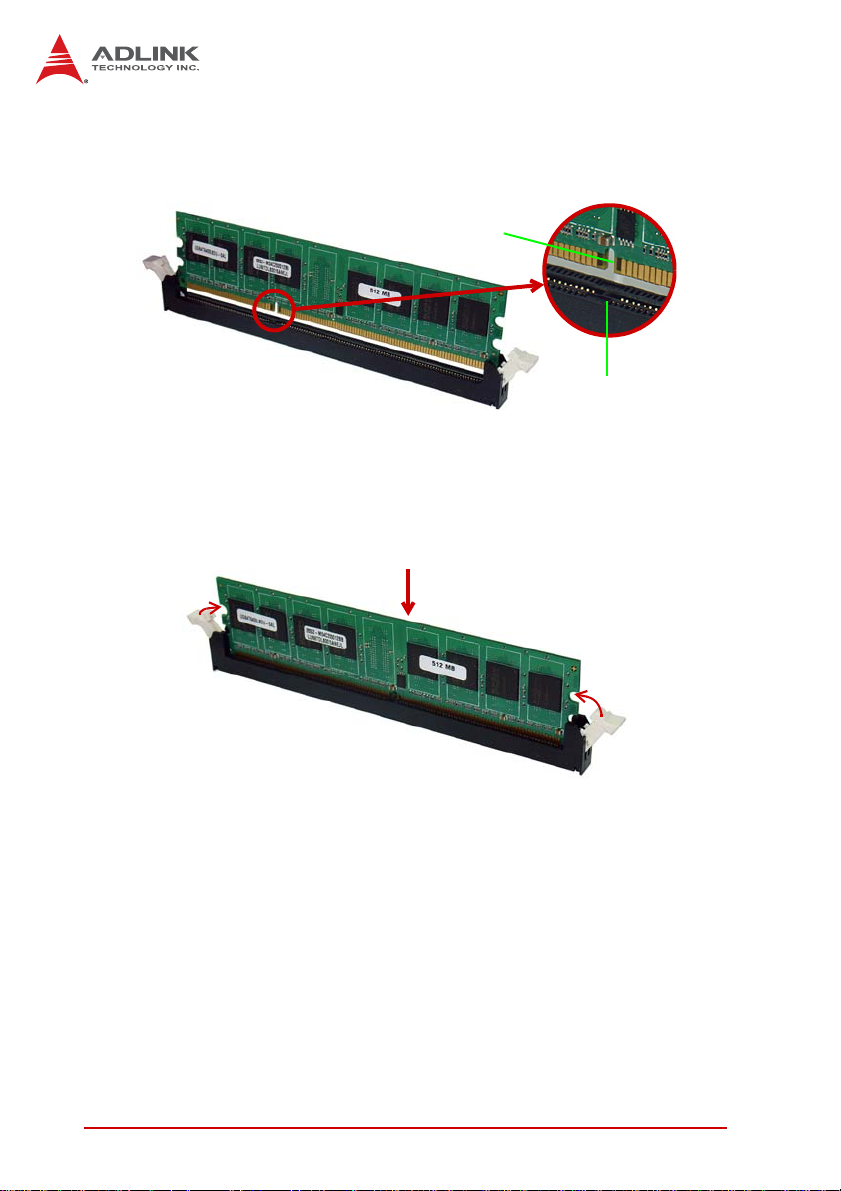
3. Align the memory module on the socket making sure
that the notch matches the break on the socket.
Notch
Break
4. Insert the module firmly into the slot until the retaining
clips snap back inwards and the module is securely
seated.
34 Getting Started
Page 49

M-321
3.4 Driver Installation
The M-321 drivers for Windows XP 32-bit are located in the following directories on the Driver DVD, or can be downloaded from
the ADLINK website (http://www.adlinktech.com):
Chipset X:\
Display X:\
LAN X:\
Audio X:\
Industrial Motherboard
Industrial Motherboard
Industrial Motherboard
Industrial Motherboard
\M-321\Chipset\infinst_autol.exe
\M-321\VGA\win2k_xp\setup.exe
\M-321\Ethernet\PRO2KXP_v14_0.exe
\M-321\Audio\WDM_R207\setup.exe
Follow the instructions below to install the required M-321 drivers:
1. Install the Windows operating system before installing any
driver. Most standard I/O device drivers are installed during
Windows installation.
2. Insta ll the Chipset driver by running the program
infinst_autol.exe. Follow the instructions given and reboot
when instructed.
3. Insta ll the Display driver and utilities by running the program
setup.exe. Follow the instructions given and reboot when
instructed.
4. Insta ll the LAN driver by running the program
PRO2KXP_v14_0.exe. Follow the instructions given and
reboot if required.
5. Install the Audio driver by running the program setup.exe. Follow
the instructions given and reboot if required.
Getting Started 35
Page 50

This page intentionally left blank.
36 Getting Started
Page 51

4 BIOS Setup
The following chapter describes basic navigation for the
AMIBIOS®8 BIOS setup utility.
4.1 Starting the BIOS
To enter the setup screen, follow these steps:
1. Power on the motherboard
2. Press the < Delete > key on your keyboard when you
see the following text prompt:
< Press DEL to run Setup >
3. After you press the < Delete > key, the main BIOS setup
menu displays. You can access the other setup screens
from the main BIOS setup menu , such as Chipset and
Power menus.
M-321
Note: In most cases, the < Delete > key is used to invoke the setup
screen. There are several cases that use other keys, such as
< F1 >, < F2 >, and so on.
BIOS Setup 37
Page 52
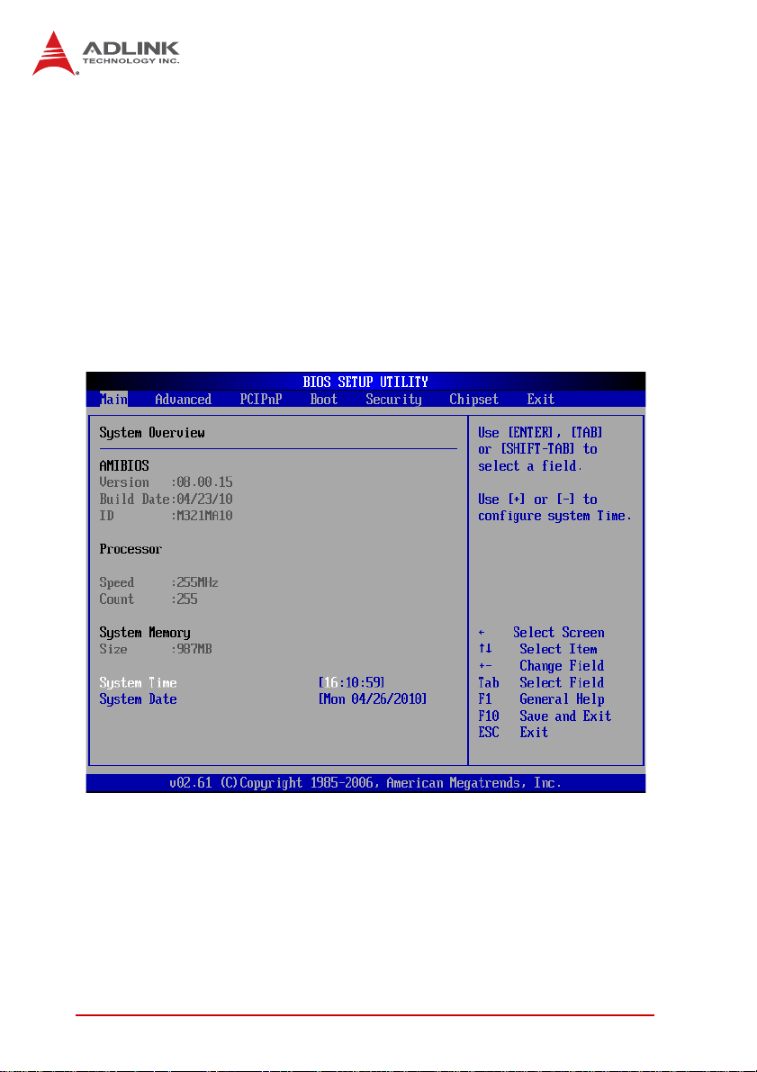
Setup Menu
The main BIOS setup menu is the first screen that you can navigate. Each main BIOS setup menu option is described in this
user’s guide.
The Main BIOS setup menu screen has two main frames. The left
frame displays all the options that can be configured. “Grayed”
options cannot be configured, “Blue” options can be.
The right frame displays the key legend. Above the key legend is
an area reserved for a text message. When an option is selected
in the left frame, it is highlighted in white. Often a text message will
accompany it.
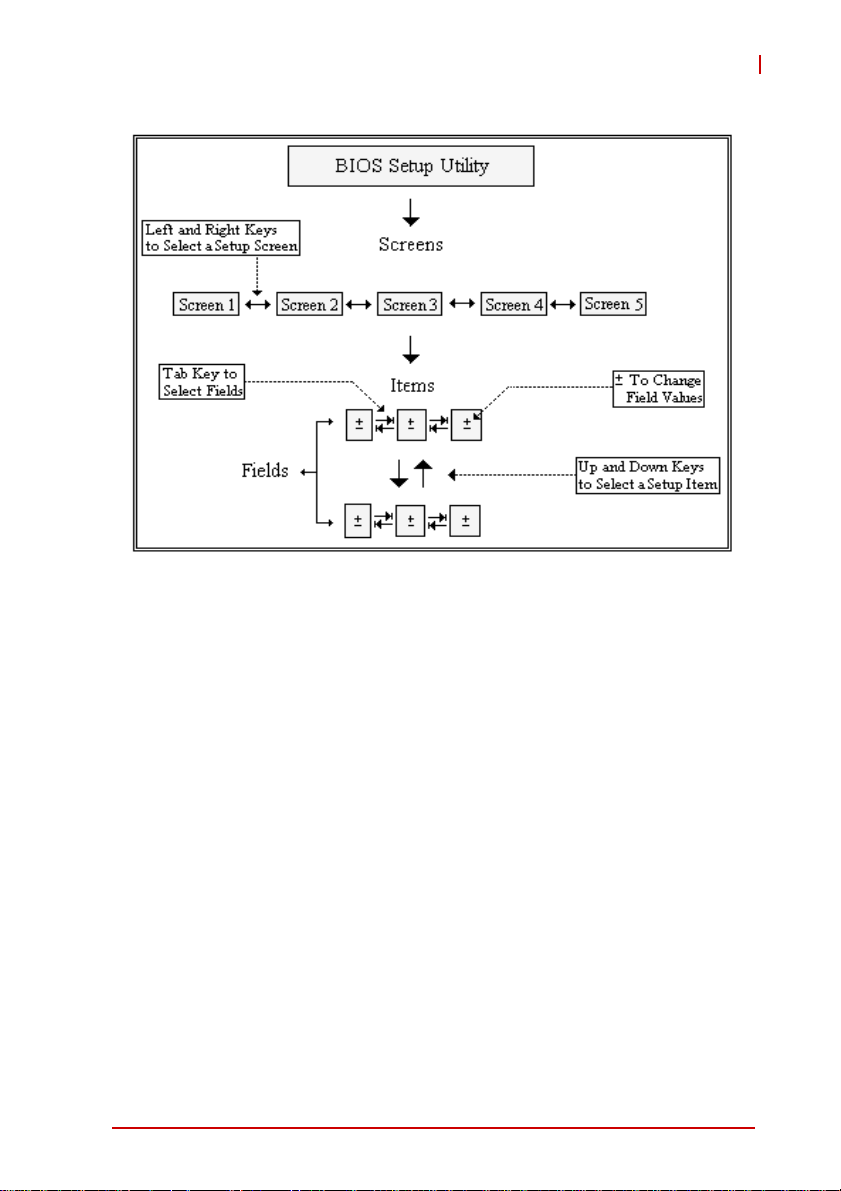
Navigation
The BIOS setup/utility uses a key-based navigation system called
hot keys. Most of the BIOS setup utility hot keys can be used at
any time during the setup navigation process.
These keys include < F1 >, < F10 >, < Enter >, < ESC >, < Arrow >
keys, and so on. .
38 BIOS Setup
Page 53
M-321
Note: There is a hot key legend located in the r ight frame on most
setup screens.
The < F8 > key on your keyboard is the Fail-Safe key. It is not displayed on the key legend by default. To set the Fail-Safe settings
of the BIOS, press the < F8 > key on your keyboard. It is located
on the upper row of a standard 101 keyboard. The Fail-Safe settings allow the motherboard to boot up with the least amount of
options set. This can lessen the probability of conflicting settings.
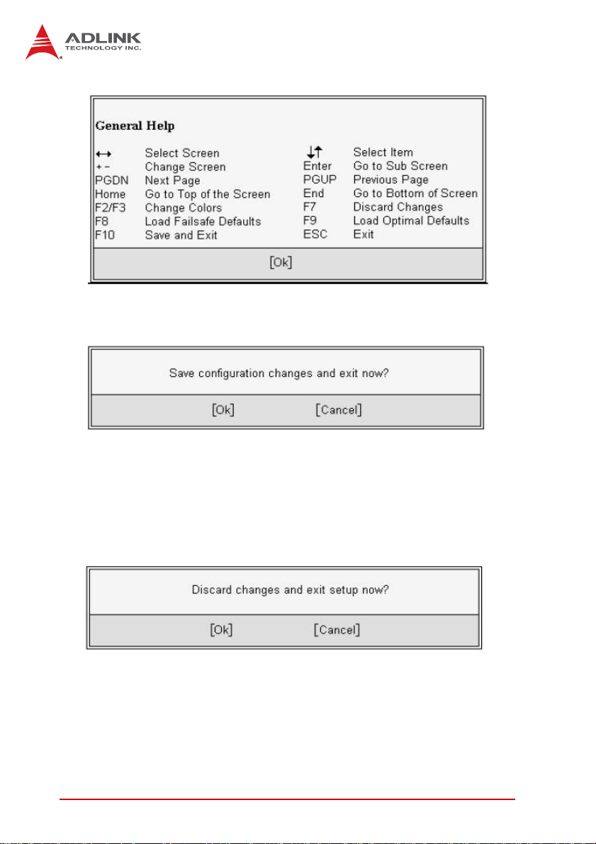
Hotkey Descriptions
F1 The < F1 > key allows you to display the General Help
screen.
Press the < F1 > key to open the General Help screen.
BIOS Setup 39
Page 54
F10 Th e < F10 > key allo ws yo u to save any changes you have
made and exit Setup. Press the < F10 > key to save your
changes. The following screen will appear:
Press the < Enter > key to save the configuration and exit.
You can also use the < Arrow > key to select Cancel and
then press the < Enter > key to abort this functio n and return
to the previous screen.
ESC The < Esc > key allows you to discard any changes you have
made and exit the Setup. Press the < Esc > key to exit the
setup without saving your changes. The following screen will
appear:
Press the < Enter > key to discard changes and exit. You can
also use the < Arrow > key to select Cancel and then press
the < Enter > key to abort this function and return to the previous screen.
Enter The < Enter > key allows you to display or change the setup
option listed for a particular setup item. The < Enter > key
can also allow you to display the setup sub-screens.
40 BIOS Setup
Page 55
M-321
4.2 Main Setup
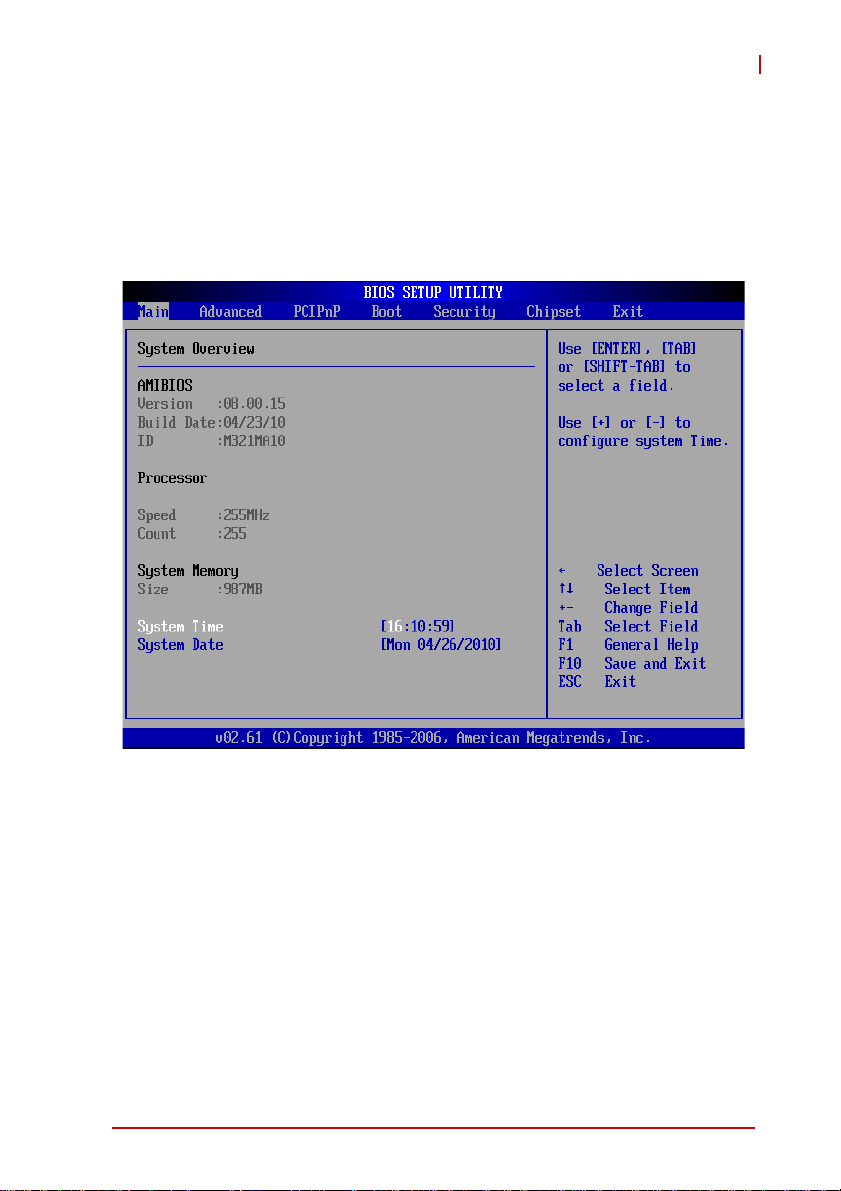
When you first enter the Setup Utility , you will enter the Main setup
screen. You can always return to the Main setup screen by selecting the Main tab. There are two Main Setup options. They are
described in this section. The Main BIOS Setup screen is shown
below.
System Time/System Date
Use this option to change the system time and date. Highlight System Time or System Date using the < Arrow > keys. Enter new values using the keyboard. Press the < Tab > key or the < Arrow >
keys to move between fields. The date must be entered in MM/
DD/YY format. The time is entered in HH:MM:SS format.
Note: The time is in 24-hour format. For example, 5:30 A.M. ap-
pears as 05:30:00, and 5:30 P.M. as 17:30:00.
BIOS Setup 41
Page 56
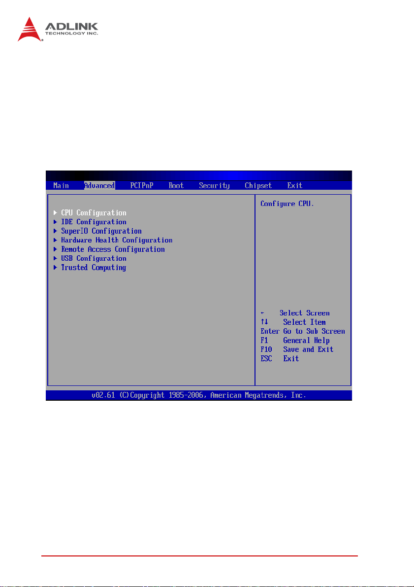
4.3 Advanced BIOS Setup
Select the Advanced tab from the setup screen to enter the
Advanced BIOS Setup screen. Yo u can select any of the items in
the left frame of the screen, such as SuperIO Configuration, to go
to the sub menu for that item. You can display an Advanced BIOS
Setup option by highlighting it using the < Arrow > keys. The
Advanced BIOS Setup screen is shown below.
The sub menus are described on the following pages.
42 BIOS Setup
Page 57
M-321
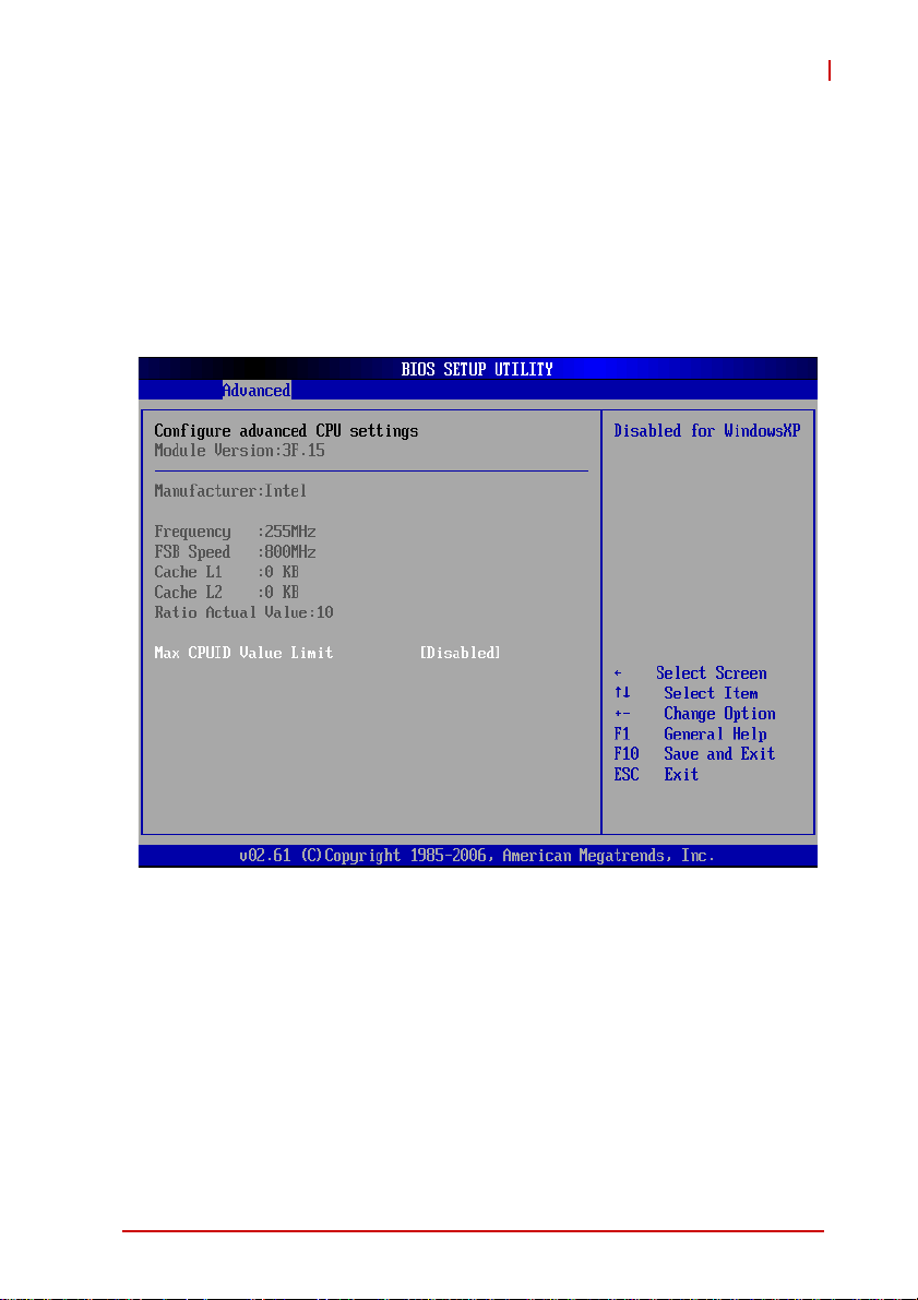
4.3.1 CPU Configuration
You can use this screen to select options for the CPU Configuration Settings. Use the up and down < Arrow > keys to select an
item. Use the < + > and < - > keys to change the value of the
selected option. A description of the selected item appears on the
right side of the screen. The settings are described on the following pages. An example of the CPU Configuration screen is shown
below.
Max CPUID Value Limit
Enable this option to allow compatibility with older operating
systems.
BIOS Setup 43
Page 58
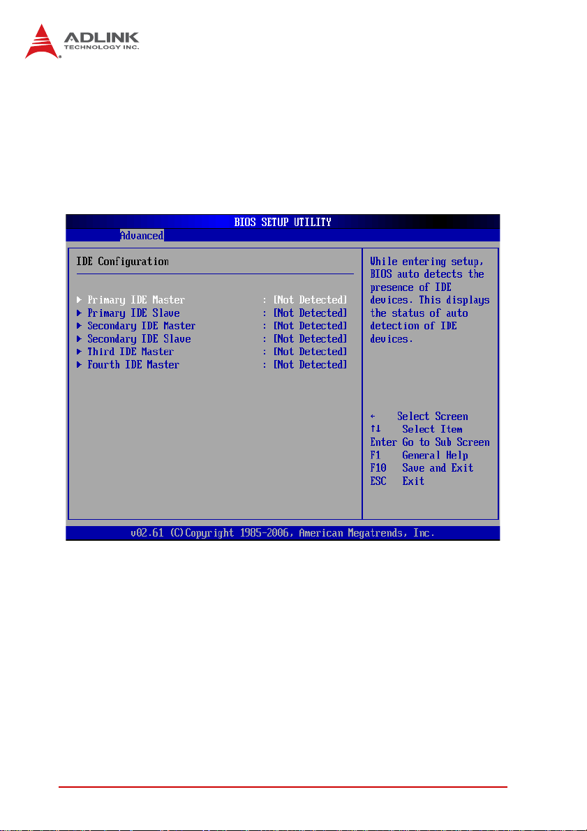
4.3.2 IDE Configuration
You can use this screen to select options for the IDE Configuration
Settings. Use the up and down < Arrow > keys to select an item.
Use the < + > and < - > keys to change the value of the selected
option. A description of the selected item appears on the right side
of the screen. The settings are described on the following pages.
An example of the IDE Configuration screen is shown below.
IDE Master/Slave
Select one of the hard disk drives to configure it. Press
< Enter > to access its sub menu.
44 BIOS Setup
Page 59
M-321
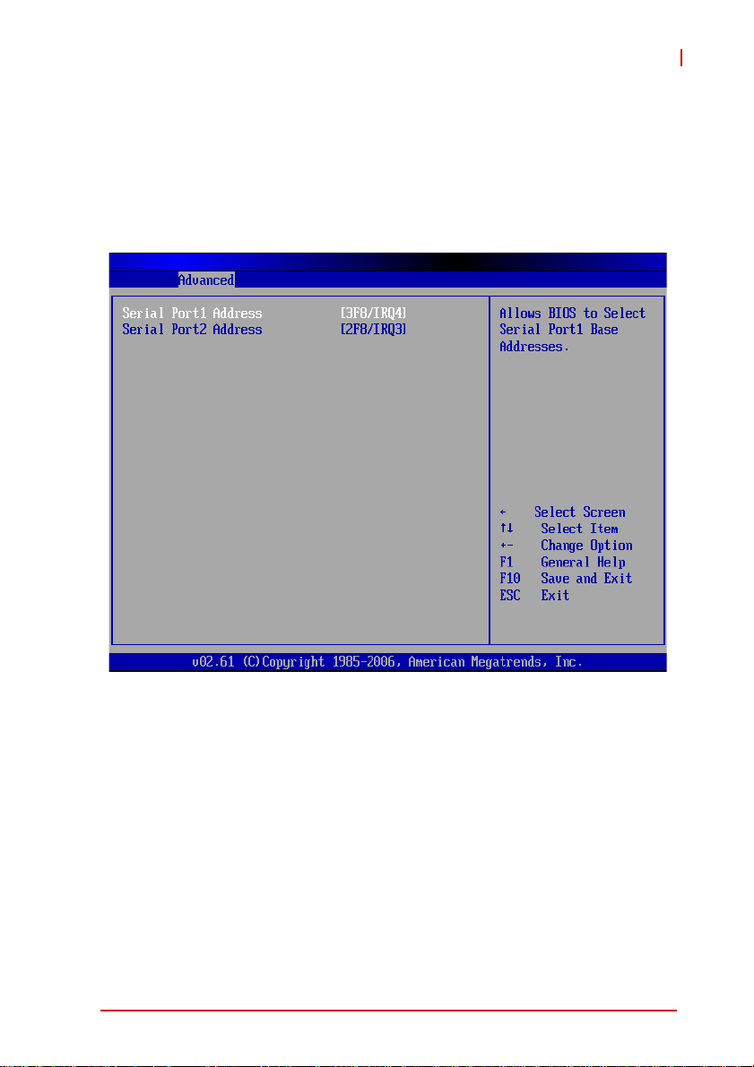
4.3.3 Super IO Configuration
Y o u can use this screen to select options for the Super IO settings.
Use the up and down < Arrow > keys to select an item. Use the <
+ > and < - > keys to change the value of the selected option. The
settings are described on the following pages. The screen is
shown below.
Serial Port1 Address
Select an address and a corresponding interrupt for Serial
Port1. Options: 3F8/IRQ4, 3E8/IRQ4, 2F8/IRQ3, 2E8/IRQ3.
Serial Port2 Address
This option specifies the base I/O port address and Interrupt
Request address of Serial Port2. The settings of Serial Port2
are the same as Serial Port1. However, the setting used by
Serial Port1 will not be available for Serial Port2. For example,
if Serial Port1 uses 3F8/IRQ4, the option, the 3F8/IRQ4 will not
appear in the options of Serial Port2.
BIOS Setup 45
Page 60
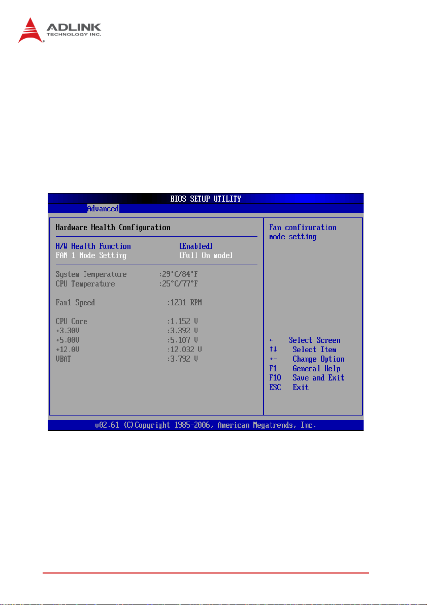
4.3.4 Hardware Health Configuration
This option displays the current status of all of the monitored hardware devices/components such as voltages and temperatures.
The options are Enabled and Disabled.
Three modes are provided for the CPU Fan (Fan1): Full On mode,
Automatic mode, and PWM Manually mode. Full On mode runs
the fan at full speed. Automatic mode is Smart Fan mode. PWM
Manually mode runs the fan at the set speed.
Full On mode
46 BIOS Setup
Page 61
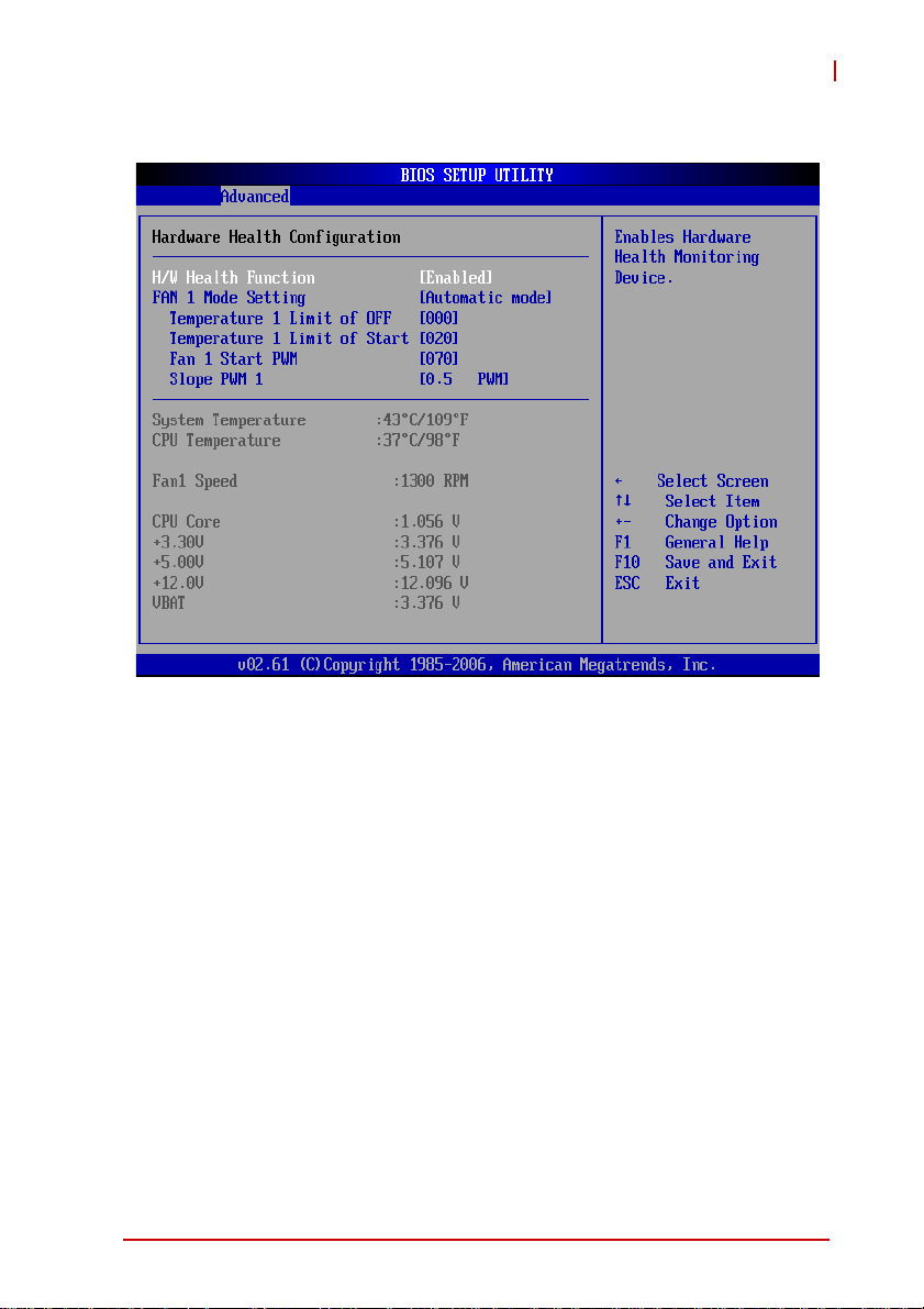
Automatic mode
M-321
Temperature 1 Limit of OFF
When the temperature (°C) is higher than the set value, Fan1
will run at Start PWM speed. When the temperature is lower
than the set value, Fan1 will stop.
Temperature 1 Limit of Start
When the temperature (°C) is higher than the set value, Fan1
will increase its speed by Slope PWM 1 value.
Fan 1 Start PWM
Sets a value to control the fan speed be tween Limit of OFF and
Limit of Start. Minimum is 0 and Maximum is 127.
Slope PWM 1
The Slope PWM Value sets the rate of increase the fan speed
when the temperature is above Limit of Start.
BIOS Setup 47
Page 62
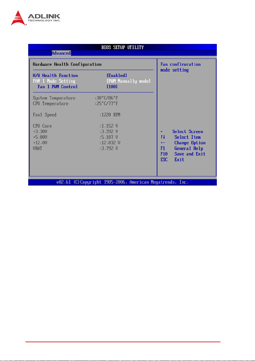
PWM Manually mode
Fan 1 PWM Control
Sets a value to control the fan speed. Minimum is 0 and Maximum is 127.
48 BIOS Setup
Page 63
M-321
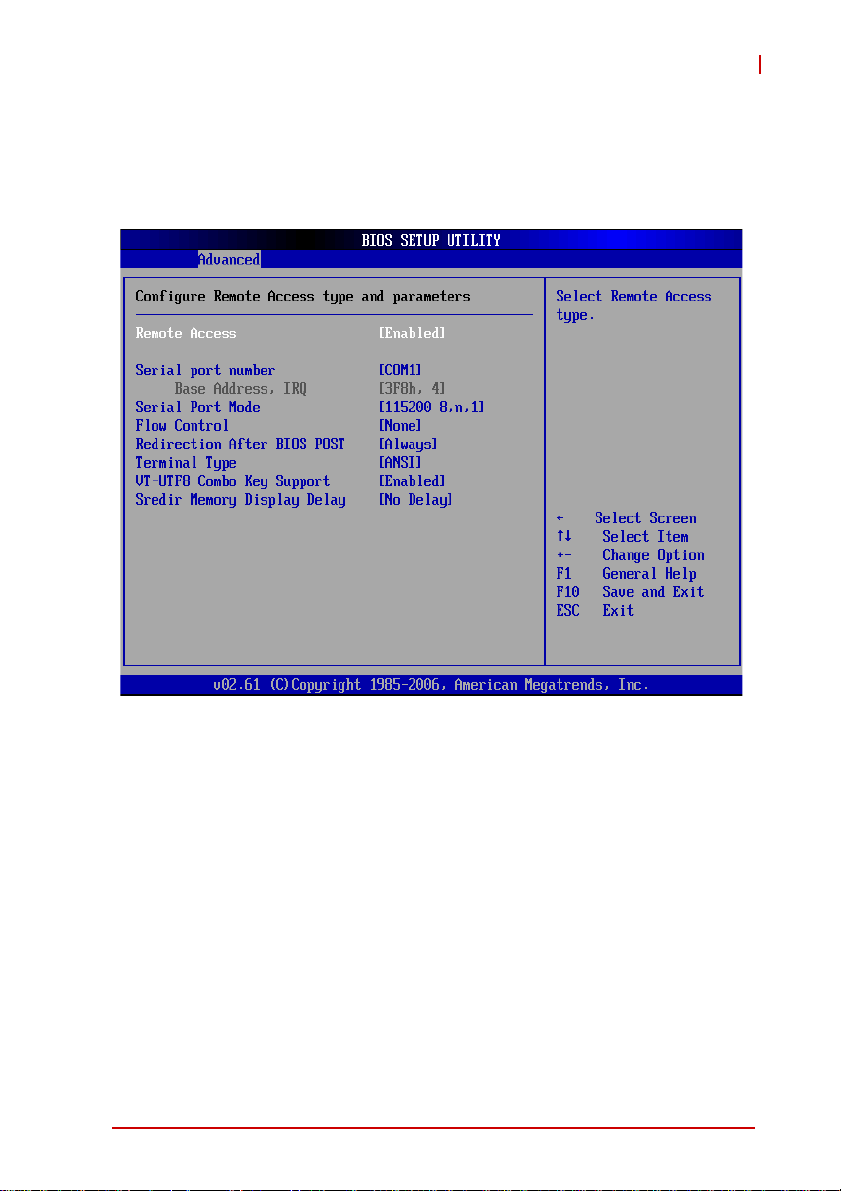
4.3.5 Remote Access Configuration
Remote access configuration provides the settings to allow remote
access by another computer to get POST messages and send
commands through serial port access.
Remote Access
Select this option to Enable or Disable the BIOS remote access
feature.
Note: Enabling Remote Access requires a dedicated serial port connec-
tion. Once both serial ports are configured to disabled, you should
set this value to Disabled or it may cause abnormal boot.
Serial Port Number
Select the serial port you want to use for the remote access
interface. You can set the value for this option to COM1 or
COM2.
Note: If you have changed the resource assignment of the serial ports in
Advanced> SuperIO Configuration, you must Save Changes and
Exit, reboot the system, and enter the setup menu again in order to
see those changes
BIOS Setup 49
reflected in the available Remote Access options.
Page 64

Serial Port Mode
Select the baud rate you want th e ser ia l po rt to use for console
redirection. The options are 115200 8,n,1; 57600 8,n,1;
19200 8,n,1; and 09600 8,n,1.
Flow Control
Set this option to select Flow Control for console redirection.
The settings for this value are None, Hardware, or Software.
Redirection After BIOS POST
This option allows you to set Redirection configuration after
BIOS POST. The settings for this value are Disabled, Boot
Loader, or Always.
X Disabled: Set this value to turn off the redirection after
POST
X Boot Loader: Set this value to allow the redirection to be
active during POST and Boot Loader.
X Always: Set this value to allow the redirection to be always
active.
Terminal Type
This option is used to select either VT100/VT-UTF8 or ANSI
terminal type. The settings for this value are ANSI, VT100, or
VT-UTF8.
VT-UTF8 Combo Key Support
This option enables VT-UTF8 Combination Key Support for
ANSI/VT100 terminals. The settings for this value are Enabled
or Disabled.
Sredir Memory Display Delay
This option gives the delay i n se co nd s to di sp l ay m emo ry in f ormation. The options for this value are No Delay, D e l a y 1 S ec ,
Delay 2 Sec, or Delay 4 Sec.
50 BIOS Setup
Page 65
M-321
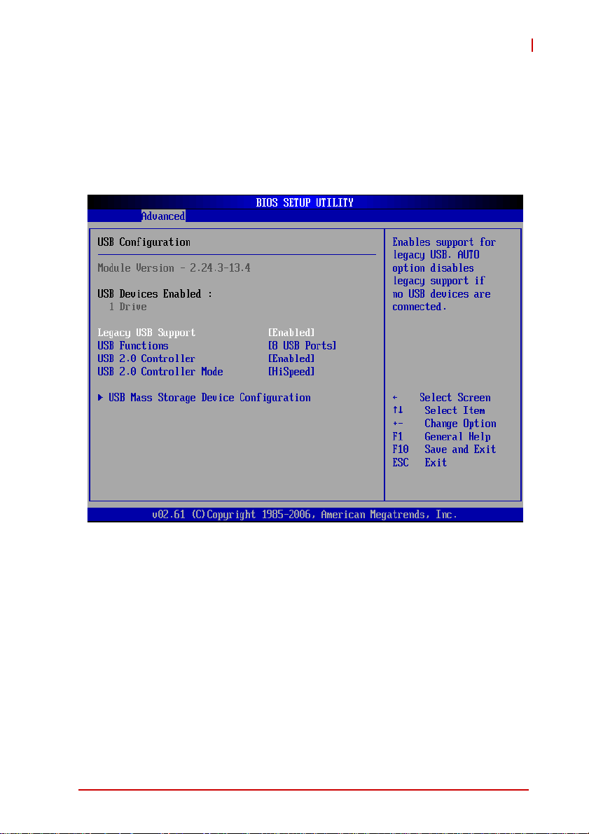
4.3.6 USB Configuration
You can use this screen to select options for the USB Configuration. Use the up and down < Arrow > keys to select an item. Use
the < + > and < - > keys to change the value of the selected
option. The settings are described on the following pages. The
screen is shown below.
Legacy USB Support
Legacy USB Support refers to USB mouse and keyboard support. Normally if this option is not enabled, any attached USB
mouse or USB keyboard will not become available until a USB
compatible operating system is fully booted with all USB drivers loaded. When this option is enabled, any attached USB
mouse or USB keyboard can control the system even when
there are no USB drivers loaded on the system. Set this value
to enable or disable the Legacy USB Support.
X Disabled: Set this value to prevent the use of any USB
device in DOS or during system boot.
BIOS Setup 51
Page 66

X Enabled: Set this value to allow the use of USB devices
during boot and while using DOS.
X Auto: This option auto detects USB Keyboards or Mice and
if found, allows them to be utilized during boot and while
using DOS.
USB Functions
Set this value to allow the system to Disable or select the number of onboard USB ports.
USB 2.0 Controller
Enables/disables USB 2.0 functionality to all USB ports. If USB
Function is set to Disabled, this option has no effect.
USB 2.0 Controller Mode
The USB 2.0 Controller Mode con figures the data rate of the
USB port. The options are FullSpeed (12 Mbps) and HiSpeed
(480 Mbps).
USB Mass Storage Device Configuration
This is a submenu for configuring the USB Mass S tor age Class
Devices when BIOS finds they are in use on USB ports. Emulation Type can be set according to the type of attached USB
mass storage device(s). If set to Auto, USB devices less than
530MB will be emulated as Floppy and those greater than
530MB will remain as hard drive. The Forced FDD option can
be used to force a hard disk type drive (such as a Zip drive) to
boot as FDD.
52 BIOS Setup
Page 67
M-321
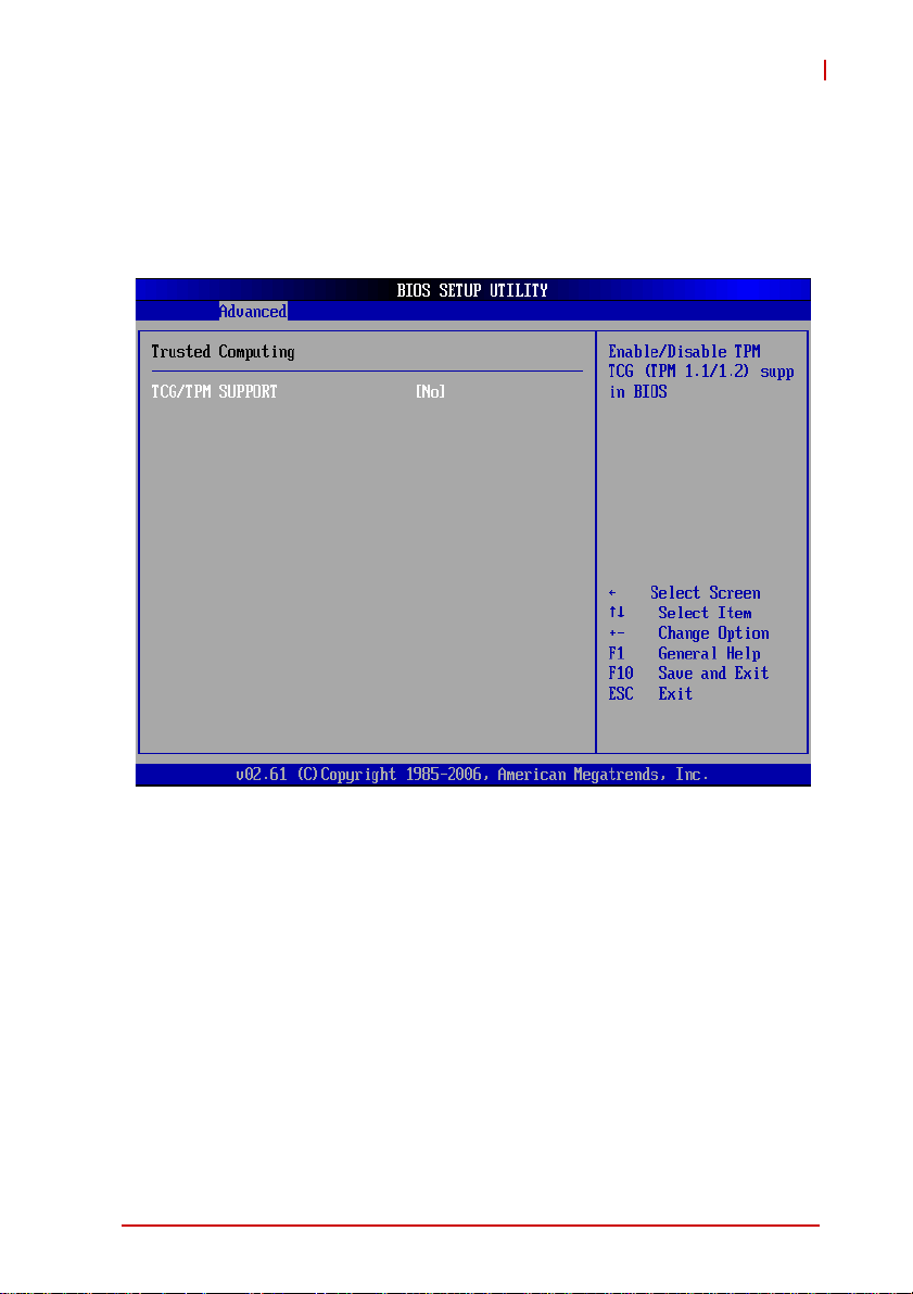
4.3.7 Trusted Computing
Trusted computing is an industry standard to make personal computers more secure through a dedicated hardware chip, called a
Trusted Platform Module (TPM). This option enables or disables
the TPM support.
BIOS Setup 53
Page 68
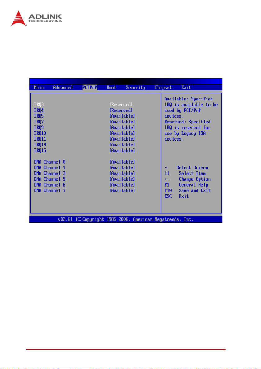
4.4 PCI/PnP Settings
Select the PCI/PnP tab from the setup screen to enter the Plug
and Play BIOS Setup screen. You can display a Plug and Play
BIOS Setup option by highlighting it using the < Arrow > keys. The
Plug and Play BIOS Setup screen is shown below.
4.4.1 IRQ/DMA
Set this value to allow the IRQ settings to be modified. Available –
This setting allows the specified IRQ/DMA to be used by a PCI/
PnP device. Reserved – This setting allows the specified IRQ/
DMA to be used by a legacy ISA device.
54 BIOS Setup
Page 69
M-321
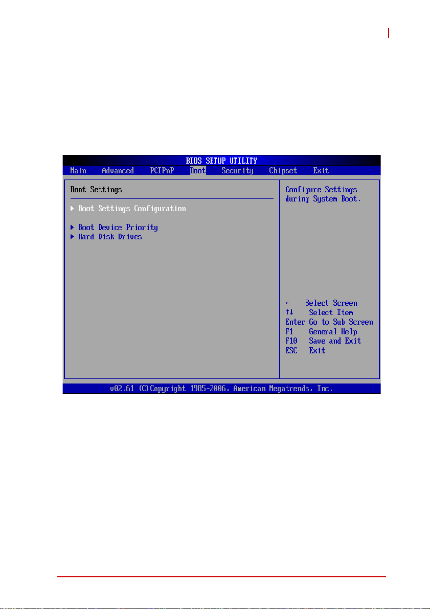
4.5 Boot Settings
Select the Boot tab from the setup screen to enter the Boot BIOS
Setup screen. You can select any of the items in the left frame of
the screen, such as Boot Dev i ce Priority, to go to the sub menu for
that item. You can display a Boot BIOS Setup option by highlighting it using the < Arrow > keys. The Boot Settings screen is shown
below:
4.5.1 Boot Settings Configuration
Use this screen to select options for the Boot Settings Configuration. Use the up and down <Arrow> keys to sel ect an it em. Use t he
<Plus> and <Minus> keys to change the value of the selected
option. The settings are described on the following pages. The
screen is shown below.
BIOS Setup 55
Page 70
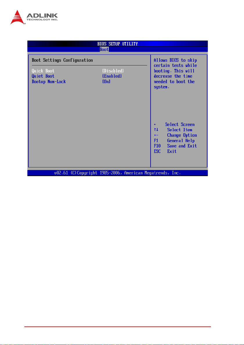
Quick Boot
Enabling this setting will cause the BIOS power-on self test
routine to skip some of its tests during bootup fo r fa st er s yst em
boot.
Quiet Boot
When this feature is enabled, the BIOS will display the fullscreen logo during the boot-up sequence, hiding normal POST
messages.
When it is disabled, the BIOS will display the normal POST
messages, instead of the full-screen logo.
Bootup Num-Lock
This setting is to set the Num Lock status when the system is
powered on. Setting to [On] will turn on the Num Lock key
when the system is powered on. Setting to [Off] will allow users
to use the arrow keys on the numeric keypad.
56 BIOS Setup
Page 71

4.5.2 Boot Device Priority
The items allow you to set the sequence of boot devices where
BIOS attempts to load the disk operating system. First press
<Enter> to enter the sub-menu. Then you may use the arrow
keys to select the desired device, then press <+>, <-> or
<PageUp>, <PageDown> key to move it up/down in the priority
list.
4.5.3 Boot Device Group s
The Boot devices are listed in groups by device type. First
press <Enter> to enter the sub -menu. Then you may use the
arrow keys to select the desired device, then press <+>, <-> or
<PageUp>, <PageDown> key to move it up/down in the priority
list. Only the first device in each device group will be available
for selection in the Boot Device Priority option.
M-321
BIOS Setup 57
Page 72
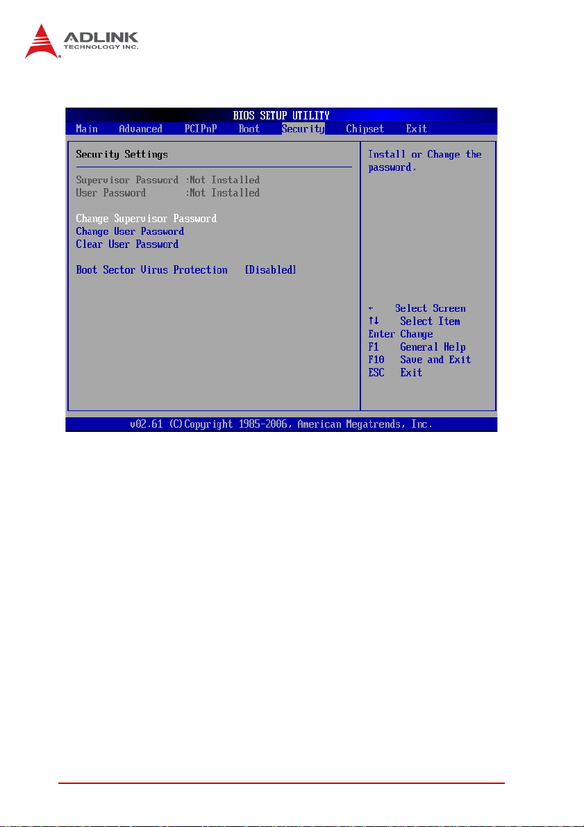
4.6 Security Setup
Password Support
Two Levels of Password Protection
Provides both a Supervisor and a User password. If you use
both passwords, the Supervisor password must be set first.
The system can be configured so that all users must enter a
password every time the system boots or when Setup is executed, using either or either the Supervisor password or User
password.
The Supervisor and User passwords activate two different levels of password security. If you select password support, you
are prompted for a one to six character password. Type the
password on the keyboard. The password does not appear on
the screen when typed. Make sure you write it down. If you forget it, you must drain NVRAM and re-configure.
58 BIOS Setup
Page 73

M-321
Remember the Password
Keep a record of the new password when the password is
changed. If you forget the password, you must erase the system configuration information in NVRAM.
To access the sub menu for the following ite m s, s ele ct th e item
and press < Enter >:
X Change Supervisor Password
X Change User Password
X Clear User Password
Supervisor Password
Indicates whether a supervisor password has been set.
User Password
Indicates whether a user password has been s et .
Change Supervisor Password
Select this option and press < Enter > to access the sub menu.
You can use the sub menu to change the supervisor password.
Change User Password
Select this option and press < Enter > to access the sub menu.
You can use the sub menu to change the user password.
Clear User Password
Select this option and press < Enter > to access the sub menu.
You can use the sub menu to clear the user password.
Change Supervisor Password
Select Change Supervisor Password from the Security Setup
menu and press < Enter >.
Enter New Password:
Type the password and press < Enter >. The screen does not display the characters entered. Retype the password as prompted
BIOS Setup 59
Page 74

and press < Enter >. If the password confirmation is incorrect, an
error message appears. The password is stored in NVRAM after
completes.
Change User Password
Select Change User Password from the Security Setup menu and
press < Enter >.
Enter New Password:
Type the password and press < Enter >. The screen does not dis play the characters entered. Retype the password as prompted
and press < Enter >. If the password confirmation is incorrect, an
error message appears. The password is stored in NVRAM after
completes.
60 BIOS Setup
Page 75
M-321
4.7 Chipset Setup
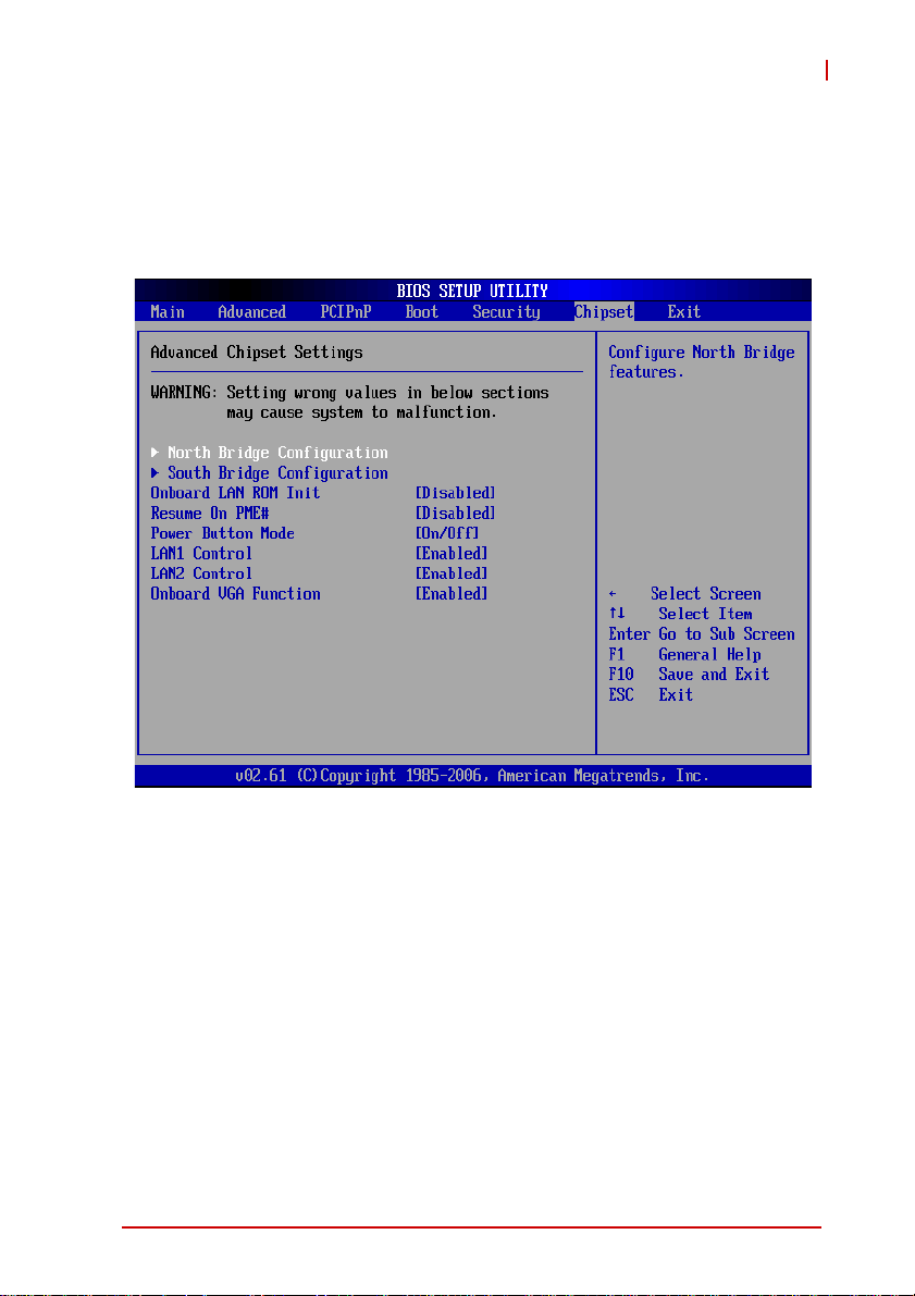
Select the Chipset tab from the setup screen to enter the Chipset
BIOS Setup screen. You can select any of the items in the left
frame of the screen to go to the sub menu for that item. The
Chipset BIOS Setup screen is shown below.
BIOS Setup 61
Page 76
4.7.1 North Bridge Configuration
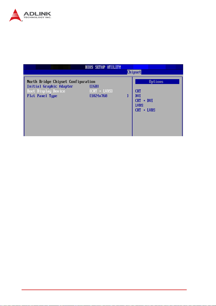
You can use this screen to select options for the No rth Bridge Configuration. Use the up and down < Arrow > keys to select an item.
Use the < Plus > and < Minus > keys to change the value of the
selected option.
Initial Graphic Adapter
Select which graphics controller to use as the primary boot
device.
X IGD: Integrated graphics only.
X PCI/IGD: Detect PCI graphics first, then integrated graphics
(PCI includes PCI slot and PCI Express x1/x4 slot, PCI will
be first).
Boot Display Device
This item allows you to select the boot display device. The
options are CRT, DVI, CRT+DVI, LVDS, and CRT+LVDS
Flat Panel Type
When LVDS is selected from Boot Displa y Device, this option
allows you to set the resolution of the LVDS interface. The
options are 640x480, 800x600, 1024x768, 1280x1024.
62 BIOS Setup
Page 77

M-321
4.7.2 South Bridge Configuration
You can use this screen to select options for the South Bridge
Configuration. Use the up and down <Arrow> keys to select an
item. Use the <Plus> and <Minus> keys to change the value of the
selected option.
HDA Controller
Set this value to Enable/Disable the HDA Controller.
Restore on AC Power Loss
Determines which state the computer enters when AC power is
restored after a power loss. The options for this value are Last
State, Power On and Power Off.
X Power Off: Set this value to always power off the system
while AC power is restored.
X Power On: Set this value to always power on the system
while AC power is restored.
X Last State: Set this value to power off/on the system
depending on the last system power state while AC power
is restored.
BIOS Setup 63
Page 78

4.7.3 Advanced Chipset Settings
You can use this screen to select options for Chipset Configuration. Use the up and down < Arrow > keys to select an item. Use
the < Plus > and < Minus > keys to change the value of the
selected option.
Onboard LAN ROM Init
Enable the onboard LAN’s PXE ROM to enable boot from LAN.
The options are Enabled and Disabled.
Resume On PME#
This option specifies if the PME#. event will generate a system
wake event. The options are Enabled and Disabled.
Power Button Mode
This option specifies the effect when the power button pressed
(On/Off, or Suspend).
X On/Off: The system is powered down immediately i f the power
button is pressed.
X Suspend: The system is powered down if the power button is
pressed for more than four seconds. Pressing the button
momentarily (for less than 4 seconds) will put the system in
"suspend" mode.
LAN1/2 Control
This item allows the user to enable/disable the onboard LAN.
On Board VGA Function
This item allows the user to enable/disable the built-in graphics.
64 BIOS Setup
Page 79
M-321
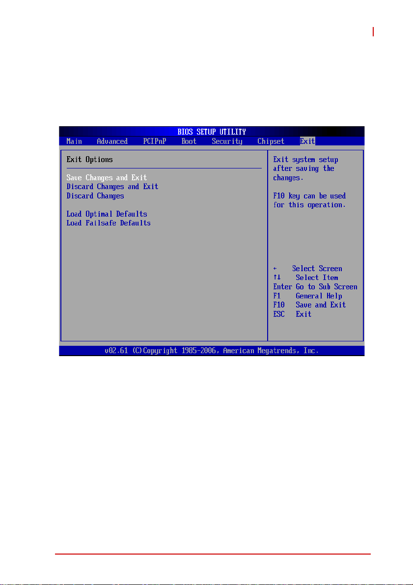
4.8 Exit Menu
Select the Exit tab from the setup screen to enter the Exit BIOS
Setup screen. You can display an Exit BIOS Setup option by highlighting it using the < Arrow > keys. The Exit BIOS Setup screen is
shown below.
Save Changes and Exit
When you have completed the system configuration changes,
select this option to leave Setup and reboot the computer so the
new system configuration parameters can take effect.
Save Configuration Changes and Exit Now?
[Ok] [Cancel]
appears in the window. Select Ok to save changes and exit.
Discard Changes and Exit
Select this option to quit Setup without making any permanent
changes to the system configuration.
BIOS Setup 65
Page 80

Discard Changes and Exit Setup Now?
[Ok] [Cancel]
appears in the window. Select Ok to discard changes and exit.
Discard Changes
Select Discard Changes from the Exit menu and press < Enter >.
Select Ok to discard changes.
Load Optimal Defaults
Automatically sets all Setup options to a complete set of default
settings when you select this option. The Optimal settings are
designed for maximum system performance, but may not work
best for all computer applications. In particular, do not use the
Optimal Setup options if your computer is experiencing system
configuration problems.
Select Load Optimal Defaults from the Exit menu and press
< Enter >.
Select Ok to load optimal defaults.
Load Failsafe Defaults
Automatically sets all Setup options to a complete set of default
settings when you select this option. The Failsafe settings are
designed for maximum system stability, but not maximum performance. Select the FailSafe Setup options if your computer is
experiencing system configuration problems.
Select Load Fail-Safe Defaults from the Exit menu and press
< Enter >.
Load FailSafe Defaults?
[Ok] [Cancel]
appears in the window. Select Ok to load FailSafe defaults.
66 BIOS Setup
Page 81

NuPRO-E330
Appendix A - Watchdog Timer
The following is a sample program for configuring the M-321’s
watchdog timer.
A.1 Sample Code
static unsigned int IT8718_ioPort = 0x2e;
void Enter_IT8718_Config(unsigned int flag)
{
if(flag) IT8718_ioPort = 0x4e;
switch(IT8718_ioPort)
{
case 0x2E: //Address port = 0x2E, enter keys =
0x87, 0x01, 0x55, 0x55
outportb(0x2E, 0x87);
outportb(0x2E, 0x01);
outportb(0x2E, 0x55);
outportb(0x2E, 0x55);
break;
case 0x4E: //Address port = 0x4E, enter keys =
0x87, 0x01, 0x55, 0xAA
outportb(0x4E, 0x87);
outportb(0x4E, 0x01);
outportb(0x4E, 0x55);
outportb(0x4E, 0xAA);
break;
default:
break;
}
}
void Exit_IT8718_Config(unsigned int flag)
{
if(flag) IT8718_ioPort = 0x4e;
outportb(IT8718_ioPort, 0x02);
outportb(IT8718_ioPort+1, 0x02);
}
void Get_IT8718_ID(unsigned int &ID1, unsigned int &ID2)
Watchdog Timer 67
Page 82

{
outportb(IT8718_ioPort, 0x20);
ID1 = inportb(IT8718_ioPort+1);
outportb(IT8718_ioPort, 0x21);
ID2 = inportb(IT8718_ioPort+1);
}
void IT8718_WDTRun(unsigned long count_value)
{
unsigned long tempCount;
unsigned int registerValue;
outportb(IT8718_ioPort, 0x07);
outportb(IT8718_ioPort+1, 0x07);// Device 7
if(count_value >= 60)
{
outportb(IT8718_ioPort, 0x72);
registerValue = inportb(IT8718_ioPort+1);
registerValue &= 0x7f;
registerValue |= 0x40; //enable WDT output through
KBRST
outportb(IT8718_ioPort+1, registerValue); // set
WDT count is minute
tempCount = count_value / 60;
if((count_value%60) > 30)
tempCount++;
if(tempCount > 65535)
tempCount = 65535;
printf("WDT timeout in %d minutes.\n", tempCount);
}
else
{
outportb(IT8718_ioPort, 0x72);
registerValue = inportb(IT8718_ioPort+1);
registerValue |= 0x80;
tempCount = count_value;
if(tempCount != 0)
{
printf("WDT timeout in %d seconds.\n",
tempCount);
68 Watchdog Timer
Page 83

NuPRO-E330
registerValue |= 0x40; //Enable WDT output
through KBRST
}
else
{
printf("WDT is Disabled.\n");
registerValue &= 0xbf; //Disable WDT output
through KBRST
}
outportb(IT8718_ioPort+1, registerValue); // set
WDT count is second
}
outportb(IT8718_ioPort, 0x71);
registerValue = inportb(IT8718_ioPort + 1);
registerValue |= 0x60;// set Mouse & Keyboard
interrupt Enable
outportb(IT8718_ioPort+1, registerValue);
outportb(IT8718_ioPort, 0x73);
outportb(IT8718_ioPort+1, tempCount); // set WDT count
LSB
tempCount = tempCount >> 8;
outportb(IT8718_ioPort, 0x74);
outportb(IT8718_ioPort+1, tempCount); // set WDT count
MSB
}
Watchdog Timer 69
Page 84

This page intentionally left blank.
70 Watchdog Timer
Page 85

Appendix B - System Resources
B.1 System Memory Map
M-321
Address Range
(decimal)
(4GB-2MB)
(4GB-18MB) –
(4GB-17MB-1)
(4GB-20MB) –
(4GB-19MB-1)
960 K – 1024 K F0000 – FFFFF 64 KB System BIOS Area
896 K – 960 K E0000 – EFFFF 64 KB Extended System BIOS Area
768 K – 896 K C0000 – DFF FF 128 KB
640 K – 768 K A0000 – BFFFF 128 KB Video Buffer & SMM space
0 K – 640 K 00000 – 9FFFF 640 KB DOS Area
Address Range
(hex)
FFE00000 –
FFFFFFFF
FEE00000 –
FEEFFFFF
FEC00000 –
FECFFFFF
Table B-1: System Memory Map
Size Description
2 MB High BIOS Area
1 MB FSB Interrupt Memory Space
1 MB APIC Configuration Space
PCI expansion ROM area
C0000 – CBFFF: Onboard VGA BIOS
CC000 – CCFFF: Intel PXE option
ROM when onboard LAN boot ROM
is enabled.
B.2 Direct Memory Access Channels
Channel Number Data Width System Resource
08-bits
18-bits
28-bits
38-bits
4 Reserved - cascade channel
5 16-bits Open
6 16-bits Open
7 16-bits Open
Parallel port
Parallel port
Diskette drive
Parallel port
(1)
(1)
(1)
(1)
Table B-2: Direct Memory Access Channels
Note(1): DMA channel 0/1/3 is selected when using parallel port. Floppy
and parallel port cannot be used at the same time.
System Resources 71
Page 86

B.3 I/O Map
Hex Range Device
000-00F, 081-09F, 0C0-0DF DMA controller 1, 8237A-5 equivalent
020-021, 0A0-0A1 Interrupt controller 1, 8259 equivalent
040-043 Timer, 8254-2 equivalent
060, 062, 064, 066, 068-06F 8042 Keyboard
061 System Speaker
070-071 Real Time Clock Controller (bit 7 - NMI mask)
0F0-0FF Co-processor error register
2F8-2FF Serial port 2
1F0-1F7, 3F6 Primary IDE Controller (AT Drive)
378-37F Parallel port
3F0-3F7 Alt. Floppy Disk Controller
3B0-3BB Mono/VGA mode video
3C0-3DF VGA registers
3F8-3FF Serial port 1
170-177, 376 Secondary IDE Channel
CF8-CFB PCI configuration address register (32 bit I/O only)
CF9 Reset Control register (8 bit I/O)
CFC-CFF PCI configuration data register
400-41F SMBUS
500-57F GPIO
800-87F SB_PM_BASE_ADDRESS
A00-A3F SIO_PME_BASE_ADDRESS
Table B-3: I/O Map
72 System Resources
Page 87

B.4 I nterrupt Request (IRQ) Lines
IRQ Lines PIC Mode
M-321
IRQ#
0 Counter 0 N/A No
1 Keyboard controller N/A No
2No N/A No
3 Serial Port 1 (COM1) IRQ3 via SERIRQ No
4
5 Serial Port 6 (COM6) IRQ5 via SERIRQ No
6 N/A IRQ6 via SERIRQ No
7 N/A IRQ7 via SERIRQ No
8 Real-time clock N/A No
9 SCI / PCI IRQ9 via SERIRQ Note (1)
10 N/A N/A No
11 N/A N/A No
12 PS/2 Mouse / PCI IRQ12 via SERIRQ Note (1)
13 Math Processor N/A No
14
15
Typical Interrupt
Resource
Serial Port 2 (COM2) /
PCI
Primary IDE controller /
PCI
Secondary IDE controller /
PCI
Table B-4: IRQ Lines PIC Mode
Connected to Pin Available
IRQ4 via SERIRQ Note (1)
IRQ14 via SERIRQ Note (1)
IRQ15 via SERIRQ Note (1)
Note(1): These IRQs can be used for PCI devices when onboard
device is disabled.
System Resources 73
Page 88

IRQ Lines APIC Mode
IRQ#
0 Counter 0 N/A No
1 Keyboard controller N/A No
2No N/A No
3 Serial Port 1 (COM1) N/A No
4
5 Serial Port 6 (COM6) IRQ5 via SERIRQ No
6 N/A IRQ6 via SERIRQ No
7 N/A IRQ7 via SERIRQ No
8 Real-time clock N/A No
9 SCI / PCI IRQ9 via SERIRQ Note (1)
10 N/A N/A No
11 N/A N/A No
12 PS/2 Mouse / PCI IRQ12 via SERIRQ Note (1)
13 Math Processor N/A No
14
15
16 N/A
17 N/A
18 N/A
Typical Interrupt
Resource
Serial Port 2 (COM2) /
PCI
Primary IDE controller /
PCI
Secondary IDE controller /
PCI / ISA
Connected to Pin Available
IRQ4 via SERIRQ Note (1)
IRQ14 via SERIRQ Note (1)
IRQ15 via SERIRQ Note (1)
PCIE Port 0/4,
UHCI Controller 4/6,
P.E.G Root Port, I.G.D,
HECI Host 1/2,
NET 2280 , PCI Slot 1
PCIE Port 1/5, KT
Controller, PCI Slot 2
PCIE Port 2,
UHCI Controller 3,
EHCI Controller 2,
SATA Host controller,
SMBus Controller,
Thermal Controller,
IDER Controller,
PCI Slot 3
Yes
Yes
Yes
74 System Resources
Page 89

M-321
IRQ#
19 N/A
20 N/A GBE controller No
21 N/A UHCI Controller 5 No
22 N/A
23 N/A
Note (1): These IRQs can be used for PCI devices when onboard
device is disabled.
Typical Interrupt
Resource
PCIE Port 3,
UHCI Controller 2/7,
SATA Host controller#1
High Definition Audio
Controller
UHCI Controller 1,
EHCI Controller 1
Ta b le B-5: IRQ Lines AP IC Mode
Connected to Pin Available
Yes
No
No
System Resources 75
Page 90

B.5 PCI Configuration Space Map
Bus # Device # Function # Routing Description
00h 00h 00h N/A
00h 01H 00h Internal P.E.G. Root Port
02h 00H FFh N/A P.E.G. Port
00h 02h 00h Internal Intel Integrated Graphics Device
00h 02h 01h Internal I.G.D., Fun#1
00h 06h 00h Internal P.E.G. #1 Root Port
03h 00h FFh Internal P.E.G. #1 Port
00h 04h 00h Internal P.E.G. #4 Root Port
00h 03h 00h Internal HECI Host #1
00h 03h 01h Internal HECI Host #2
00h 03h 02h Internal IDER Controller
00h 03h 03h Internal KT Controller
00h 16h 00h Internal VE AHCI Controller
00h 19h 00h Internal GbE Controller
00h 1Ah 00h Internal Intel USB UHCI Controller #4
00h 1Ah 01h Internal Intel USB UHCI Controller #5
00h 1Ah 02h Internal Intel USB UHCI Controller #7
00h 1Ah 07h Internal Intel U S B EHCI Controller #2
00h 1Bh 00h Internal High Definition Audio controller
00h 1Ch 00h Internal Intel ICH Express Root port #0
00h 1Ch 01h Internal Intel ICH Express Root port #1
00h 1Ch 03h Internal Intel ICH Express Root port #3
00h 1Ch 04h Internal Intel ICH Express Root port #4
00h 1Ch 05h Internal Intel ICH Express Root port #5
00h 1Dh 00h Internal Intel USB UHCI Controller #1
00h 1Dh 01h Internal Intel USB UHCI Controller #2
00h 1Dh 02h Internal Intel USB UHCI Controller #3
00h 1Dh 03h Internal Intel USB UHCI Controller #6
00h 1Dh 07h Internal Intel USB EHCI Controller #1
00h 1Eh 00h N/A Intel Hub Interface to PCI Bridge
00h 1Fh 00h N/A Intel LPC Interface Bridge
Intel Q45 GMCH Host Hub
Interface Bridge
76 System Resources
Page 91

M-321
Bus # Device # Function # Routing Description
00h 1Fh 02h Internal Intel SATA Host /Raid controller
00h 1Fh 03h Internal Intel SMBus Controller
00h 1Fh 05h Internal Intel Host SATA controller1
00h 1Fh 06h Internal Thermal Controller
04h 00h FFH Internal PCIE Port #0
05h 00h FFh Internal PCIE Port #1
06h 00h FFh Internal PCIE Port #2
07h 00h FFh Internal PCIE Port #3
08h 00h FFh Internal PCIE Port #4
09h 00h FFh Internal PCIE Port #5
01h 0Fh FFh Slot PCI Slot 1
01h 0Eh FFh Slot PCI Slot 2
01h 0Dh FFh Slot PCI Slot 3
01h 0Ch FFh Slot NET 2288
Table B-6: PCI Configuration Space Map
System Resources 77
Page 92

B.6 PCI Interrupt Routing Map
PIRQ A B C D E F G H
P.E.G Root Port INTA INTB INTC INTD
P.E.G Root Port 1 INTA INTB INTC INTD
IGD X
SATA Controller X X
SATA Controller1 X
SMBUS controller X
Thermal Controller X
HDA Controller X
GbE Controller X
VE AHCI Controller X X
HECI Host #1 X
HECI Host #2 X
IDER Controller X
KT Controller X
PCIE port 0 INTA INTB INTC INTD
PCIE port 1 INTB INTC INTD INTA
PCIE port 2 INTC INTD INTA IN TB
PCIE port 3 INTD INTA INTB INTC
PCIE port 4 INTA INTB INTC INTD
PCIE port 5 INTB INTC INTD INTA
PCI slot 1 INTA INTB INTC INTD
PCI slot 2 INTB INTC INTD INTA
PCI slot 3 INTC INTD INTA INTB
Table B-7: PCI Interrupt Routing Map
78 System Resources
Page 93

M-321
Important Safety Instructions
For user safety, please read and follow all instructions,
WARNINGS, CAUTIONS, and NOTES marked in this manual
and on the associated equipment before handling/operating the
equipment.
X Read these safety instructions carefully.
X Keep this user’s manual for future reference.
X Read the specifications section of this manual for detailed
information on the operating environment of this equipment.
X When installing/mounting or uninstalling/removing
equipment:
Z Turn off power and u nplug any power cords/cables.
X To avoid electrical shock and/or damage to equipment:
Z Keep equipment away from water or liquid sources;
Z Keep equipment away from high heat or high humidity;
Z Keep equipment properly ventilated (do not block or
cover ventilation openings);
Z Make sure to use recommended voltage and powe r
source settings;
Z Always install and operate equipment near an easily
accessible electrical socket-outlet;
Z Secure the power cord (do not place any obje ct on /ove r
the power cord);
Z Only install/attach and operate equipment on stable
surfaces and/or recommended mountings; and,
Z If the equipment will not be used for long periods of time,
turn off and unplug the equipment from its power source.
Important Safety Instructions 79
Page 94

X Never attempt to fix the equipment. Equipmen t sho u ld on ly
be serviced by qualified personnel.
A Lithium-type battery may be provided for uninterrupted, backup
or emergency power.
Risk of explosion if battery is replaced with one of an incorrect
WARNING:
type. Dispose of used batteries appropriately.
X Equipment must be serviced by authorized technicians
when:
Z The power cord or plug is damaged;
Z Liquid has penetrated the equipment;
Z It has been exposed to high humidity/moisture;
Z It is not functioning or does not function according to the
user’s manual;
Z It has been dropped and/or damaged; and/or,
Z It has an obvious sign of breakage.
80 Important Safety Instructions
Page 95

Getting Service
Contact us should you require any service or assistance.
ADLINK Technology, Inc.
Address: 9F, No.166 Jian Yi Road, Chungho City,
Taipei County 235, Taiwan
Ampro ADLINK Technology, Inc.
Address: 5215 Hellyer Avenue, #110, San Jose, CA 95138, USA
Tel: +1-408-360-0200
Toll Free: +1-800-966-5200 (USA only)
Fax: +1-408-360-0222
Email: [email protected]
ADLINK Technology Beijing
Address: ࣫ҀᏖ⍋⎔Ϟഄϰ䏃 1 োⲜ߯ࡼ E ᑻ 801 ᅸ(100085)
Rm. 801, Power Creative E, No. 1, B/D
Shang Di East Rd., Beijing, 100085 China
Tel: +86-10-5885-8666
Fax: +86-10-5885-8625
Email: [email protected]
M-321
ADLINK Technology Shanghai
Address: Ϟ⍋Ꮦⓩ⊇⋒催⾥ᡔᓔথ䩺∳䏃 333 ো 39 ᐶ 4 ሖ (200233)
4F, Bldg 39, Caoheting Science & Technology Park,
ADLINK Technology Shenzhen
Address: ⏅ഇᏖቅ⾥ᡔು催ᮄϗ䘧᭄ᄫᡔᴃು
Getting Service 81
No.333 Qinjiang Rd., Shanghai, 200233 China
A1 2 ὐ C (518057)
2F, C Block, Bldg. A1, Cyber-Tech Zone, Gao Xin Ave. Sec. 7,
High-Tech Industrial Park S., Shenzhen, 518054 China
Page 96

ADLINK Technology, Inc. (German Liaison Office)
Address: Nord Carree 3, 40477 Duesseldorf, Germany
Tel: +49-211-495-5552
Fax: +49-211-495-5557
Email: [email protected]
ADLINK Technology, Inc. (French Liaison Office)
Address: 15 rue Emile Baudot, 91300 Massy CEDEX, France
Tel: +33 (0) 1 60 12 35 66
Fax: +33 (0) 1 60 12 35 66
Email: [email protected]
ADLINK Technology Japan Corporation
Address: 151-0072 ᧲ㇺ⼱ᐈ䊱⼱㩷
1-1-2 ᦺᣣ↢ᐈ䊱⼱䊎䊦 8F
Asahiseimei Hatagaya Bldg. 8F
1-1-2 Hatagaya, Shibuya-ku, Tokyo 151-0072, Japan
Tel: +81-3-4455-3722
Fax: +81-3-5333-6040
Email: [email protected]
ADLINK Technology, Inc. (Korean Liaison Office)
Address: 昢殾柢 昢爎割 昢爎壟 1506-25 穢壊 B/D 2 猻
2F, Hando B/D, 1506-25, Seocho-Dong, Seocho-Gu,
ADLINK Technology Singapore Pte. Ltd.
Address: 84 Genting Lane #07-02A, Cityneon Design Centre,
ADLINK Technology Singapore Pte. Ltd. (Indian Liaison Office)
Address: No. 1357, "Anupama", Sri Aurobindo Marg, 9th Cross,
JP Nagar Phase I, Bangalore - 560078, India
Tel: +91-80-65605817
Fax: +91-80-22443548
Email: [email protected]
82 Getting Service
 Loading...