

Page 1
solid state
Back
Adcom GFP-555 Preamp Upgrade
In the best tradition of DIY audio, this author’s modifications significantly
upgrade a proven preamp design.
modified my Adcom GFP-555 in
a manner similar to Gary Galo’s
GFP-565 project in his series of
I
articles in audioXpress
do a “purist” upgrade like Gary—I kept
the tone controls, which now supply
a new set of output jacks, and all the
available inputs but with an upgrade to
gold jacks. I changed the tone control
op amp from the original NJM2041 to
the OPA2604. The LAB and NORM
outputs are now both DC-coupled. I
also removed the headphone amplifier,
which was a mediocre design with an
NJM4556 op amp, so I decided to save
the available watts for the new AD744/
AD810 output stage, which draws a
lot of current. The GFP-555 has even
higher gain (22.5dB) than the 565, so
the volume control wiper is well down
at normal listening levels.
The lower 14dB gain of Gar y’s
line stage was a welcome change. The
AD744/AD811 line stage was a bit
more difficult to install because the -555
1-5
. I did not
By Charles Hansen
does not have the dual-composite op
amps that the -565 has. Victor Campos recalled that the -555 was probably
designed by Nelson Pass before Victor
arrived at Adcom.
While I did not use an external power
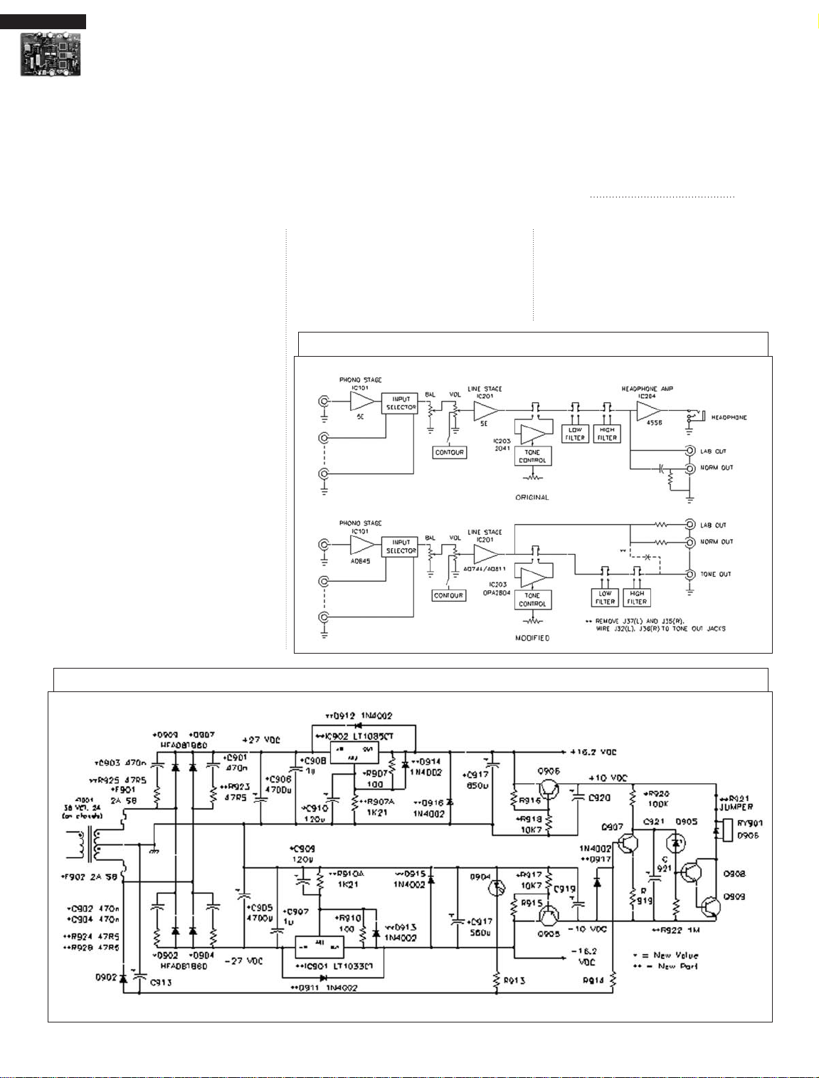
FIGURE 1: Block diagram comparing original with modification.
supply, I did upgrade the power supply,
changing to a 36V CT 2A secondary,
with a copper flux band and steel end
plates. I fit in the larger transformer by
removing the line voltage selector switch
and its extra wiring.
AE-adcom-01
FIGURE 2: Power supply schematic.
44
audioXpress
9/06 www.audioXpre ss . co m
AE-adcom-01
Page 2
I kept two of the existing plastic dualdual phono jack modules, which make
a desirable mechanical connection between the PC board and the rear panel.
These are the Tuner In/Tape 1 In pair
and the Signal Processor In/Out pair.
The former two will be active, while the
Processor pair will be strictly mechanical
and bypassed with jumpers.
Parts cost for this upgrade was about
$115, based on the parts list in Table 1.
I happened to have the GFP-555, but
I recommend using the –565 if you are
considering this type of upgrade. Follow
Gary’s articles for the purist version, but
for a “less-than-purist” modification that
retains the original I/O flexibility of the
Adcom design, this article will provide
guidelines.
I strongly suggest you obtain the service manual, for the model of preamp
you are modifying (readily available as
reprints on eBay). I mapped all the PC
board jumpers onto the schematic so I
could replace them with discrete com
ponents where necessary. I must thank
Gary Galo for his comments on my proposed modifications; he was very helpful
and provided some interesting insight
into the Adcom preamp designs of that
era.
MODIFICATIONS
Prior to making any modifications, I
verified all the DC voltages shown on
the schematic (it had sat unused for a
few years), checked that all the controls
and input/outputs were functional, gave
the Adcom a listening session, and made
a few measurements.
Figure 1 shows block diagrams for
the original GFP-555 and for my modifications. In both cases the CD, Tuner,
Tape 1, Tape 2, and Video/Aux inputs
are processed through the Listening
input selector switch, with the phono
preamp section providing one of the in
-
puts. There was also a separate Recording selector switch that coupled to the
Tape 1 and Tape 2 tape loop jacks.
Audio signals proceed from the input
switch to the Signal Processor I/O jacks,
which are furnished with removable
metal links. The next step is the Balance
control, the Mono/Stereo switch, and
the Volume control, which is equipped
with a Contour switch to the tapped volume control that could select the loudness contour function for low listening
levels. Finally, the selected audio signal
was sent on to the active line stage.
The output of the line stage can then
take a number of series paths. When the
tone controls and filters are bypassed, the
line stage is direct-coupled to the LAB
output and capacitively-coupled to the
NORM output. The headphone amp
input receives this same signal. Three
additional switches in the line output
-
PHOTO 1: GFP-555 original power supply rear.
PHOTO 2: GFP-555 original power supply front.
PHOTO 3: GFP-555 mod power supply rear.
PHOTO 4: GFP-555 mod power supply front with new
transformer.
audioXpress
September 2006 45
Page 3
signal path allow selection of the tone
controls—a Lo filter and/or a Hi filter.
The original phono preamp and line
stage ICs had a house number, “5E,”
which Victor thought was an OP37.
This would make sense, because the
OP37 is one of the few op amps whose
maximum supply rail voltage was ±22V,
and the Adcom schematic shows the
5E operating on ±21.5V rails. On the
other hand, Gary observed that with the
phono gain switch set to the lower gain
position, the circuit does not satisfy the
gain-of-5 stability requirement of the
OP37, so maybe the “5E” was an OP27.
The modified block diagram at the
bottom of Fig. 1 is essentially the same
up to the output of the line stage. At this
point the amplified signal takes two distinct paths. The first is direct-coupled to
both the LAB and NORM output jacks.
The second path uses all the switched
tone control and filter circuitry of the
original unit, but goes to another set of
output jacks that I added called Tone
Out.
You can also see that I changed all
the ICs to reflect improvements made
over the intervening years. The phono
preamp went from the 5E to an AD845.
I replaced the line stage 5E with the
aforementioned AD744/AD811 composite amplifier. The NJM2041 tone
control IC became an OPA2604. Finally,
I removed the 4556 headphone amplifier and all its passive parts, although I
left the jack in place on the front panel.
I tried unsuccessfully to fit my Headroom headphone module board6 in the
space between the transformer and the
front panel.
POWER SUPPLY
Gary used a separate power supply chassis for his GFP-565 modification, which
has the distinct advantage of lower
phono stage hum and noise. However, I
wanted to retain a one-box preamp. The
original power supply regulators were
composed of discrete transistors Q901
and Q902 that used ±32.5V raw DC
rails to derive the ±21.5V DC op amp
rails. Another set of transistor regulators,
Q905 and Q906, further stepped this
down to ±15.6V DC for the headphone
op amp, and provided 31.2V DC for the
output delay relay circuit.
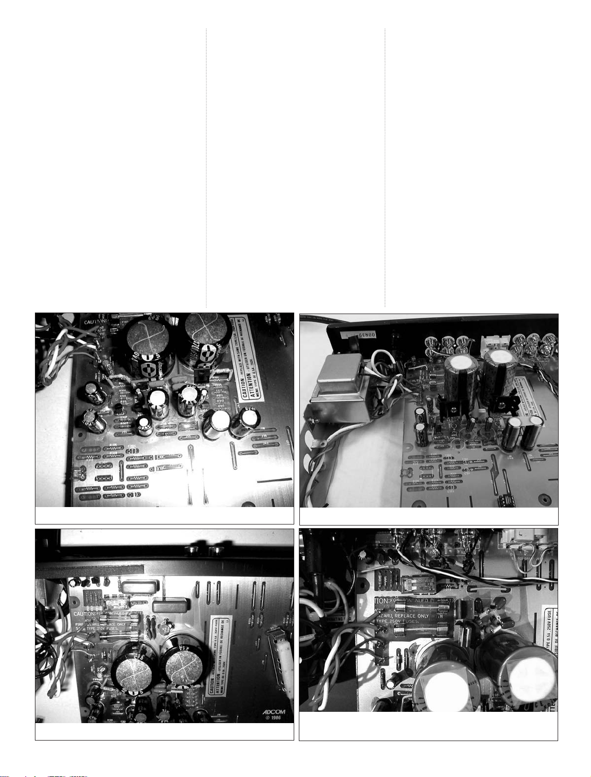
Photos 1 and 2 show the front and
rear views of the original supply. In the
foreground of Photo 1 I have already
FIGURE 3: Phono preamp schematic.
removed the components for the headphone amplifier.
My modified power supply is shown
in Fig. 2. After mapping all the jumpers onto the schematic, I replaced all the
power supply jumpers with larger wire
gauges. Next, I removed all the power
supply components from the PC board
and I replaced the Jamicon bulk filter
caps with Nichicon KZ and Panasonic HFQ types. I used LT1085CT and
LT1033CT linear regulator ICs for the
new ±16.2V DC op amp power supply
rails.
Because the delay relay has a 24V
coil, there was no need for 31.2V DC.
The original design used a 274Ω series
resistor to drop the coil voltage to 24V.
I removed the resistor and dedicated
Q905 and Q906 to a reduced ±10V DC,
which saved some power dissipation in
AE-adcom-03
FIGURE 4: Line stage schematic.
46
audioXpress
9/06 www. au di oX pr es s .c om
AE-adcom-04
Page 4

the relay coil. Gary increased
FIGURE 5: Line stage IC socket assembly.
the relay time delay, whereas
I left it the same.
Photo 3 shows the front
view of my new power supply. I placed adhesive-backed
Mylar film across pairs of
aluminum capacitors to provide them some additional
mechanical ruggedness. The
new transformer is on the left
side. Note the TO-220 heatsinks mounted on the linear
regulators. These are needed
because of the higher current
drawn by the AD744/AD811
composite line stages.
I installed the new HexFred diodes in the old snubber cap holes, and the new
snubber resistor/cap combinations in the old rectifier
bridge holes (Photo 4). Two
of the TO-220 diode mounting tabs were facing each
other, so I placed adhesivebacked Nomex on the tabs
PHOTO 5: GFP-555 mod phono stage.
to keep them from shorting
together.
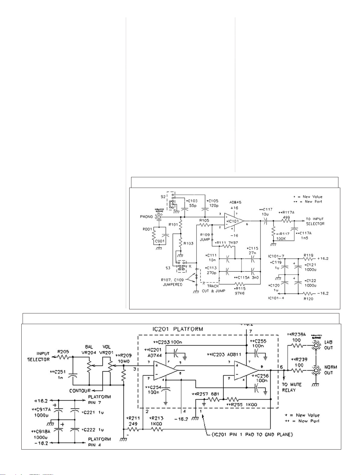
PHONO STAGE
The phono stage in Fig . 3 is the one
designed around the AD845 op amp
by Walt Jung in Analog Devices’ “Op
Amp Applications,”7 pp. 6–18. Walt also
kindly provided me with two AD845KN
op amps because the DIP package is no
longer available (Rochester Electronics
may have some NOS parts in stock). I
replaced the two 1000µF Jamicon filter
caps with Nichicon KZ, shown on the
right in Photo 5.
I remo ved 55pF caps C101 and
C1023 from the PC board and reduced
the capacitor values on the cartridge capacitive load switch to 55pF and 120pF.
This allowed me the choice of no capacitor, or one of the latter two values.
The MM/MC gain switch remained as
it was.
tors. I also drilled holes in the PC board
to add two more 1000µF Nichicon KZ
power supply filter caps for the line stages
(C917A and C918A). These are shown in
the center of Photo 5.
The line stage presented a real packaging problem. Because the GFP-555
did not use composite op amp stages,
there was much less real estate available
for the 744/811 combination. The plastic
indexing control band for the Recording
switch ran right over the top of the exit-
FIGURE 6: RIAA response error.
ing 5E op amps (Photo 6).
I needed to build a “flying bridge” plug-in module
for the AD744/AD811 composite line amp by epoxying
two 8-pin DIP sockets and an
8-pin DIP platform to a ⅛
wide copper strip. I bent the
AE-adcom-05
strip upward at each end to
allow the 744/811 assemblies
to clear selector switches S4
and S5, and the exiting PC
board components surrounding the original “5E” ICs. I
grounded the copper strip via
unused platform pin 1 so it
formed a ground plane under
the 744 and 811.
The clip-on heatsinks over
the AD811s are shown on the
right side in the photo. All
the sockets and platforms are
Garry Engineering machined
low-profile gold-plated types
we used in RF and switching
circuit brassboards at work.
A rear view drawing of the
plug-in modules and their
close clearances is shown in Fig. 5. In
his newer designs11, Walt has recommended using the AD845 in place of
the AD744, but my construction was a
bit too far along for that improvement
because the wiring between the AD744
and AD811 was now firmly anchored
in epoxy.
The tone controls, lo and hi filters,
and the contour circuitry all remain the
same as in the original unit, and I do
not show them in this article. Of course,
LINE STAGE
The line stage (Fig. 4) consists of the
AD744/AD811 composite pair that
Gary used, which is itself based on another Walt Jung design that goes back to
8-10
1992
outputs from each other with 100Ω resis-
. I isolated the LAB and NORM
audioXpress
AE-adcom-06
September 2006 47
Page 5

much progress has been made in IC
technology and cost since the original design, although the AD744 and
AD845 op amps are both listed in my
1988 ADI catalog.
LISTENING AUDITION
Gary Galo suggested that I also try the
OPA627AP in the phono stage, because it has slightly lower noise specifications than the AD845 and is readily
available in the DIP package, making
it easier for readers to install. However,
one of the weaknesses of the one-box
design is the power supply noise induced by having the phono stage inside
the same enclosure as the power supply, especially the power transformer.
At full volume, the hiss and low-level
hum were quite noticeable. Once I
started the first LP and dialed down
the volume to a comfortable listening
FIGURE 9: Line stage frequency response.
level, the modified preamp proved quieter than the original by a fair margin.
I could not really discern any difference in the noise level between the two
candidate phono stage op amps, but I
did prefer the sound of the AD845 just
a bit.
The original GFP-555 phono section was a touch tubby in the bass and
had a higher hiss level than the modified unit. The line inputs tended to-
PHOTO 6: GFP-555 mod line stage.
FIGURE 7: Phono preamp 50Hz residual.
AE-adcom-07
FIGURE 8: Phono preamp spectrum of 50Hz sine wave.
AE-adcom-09
FIGURE 10: Line stage THD + N vs. frequency.
AE-adcom-10
FIGURE 11: Line stage THD+N vs. output voltage.
48
audioXpress
AE-adcom-08
9/06 ww w.audioXpre ss .co m
AE-adcom-11
Page 6

ward a more muted high
FIGURE 12: Line stage 1kHz residual.
frequency response that became strident when I used
the tone controls to compensate. With both CD and LP
sources, the modified unit is
much easier to listen to than
the original. The midrange
especially is more detailed
and open, with better imaging and a wider and deeper
soundstage. It has also made
listening to classical music
on my FM tuner more enjoyable.
MEASUREMENTS
Once my listening sessions were over, I
swapped the AD845 for the OPA627
and ran the whole preamp on a ±24V
DC lab supply that was located across
the room. Even with the power supply connected to the raw DC rails via
three alligator clips and long lead wires,
I could measure a slightly lower noise
floor with the OPA627, so you might
want to consider it for a two-box design like Gary’s.
Phono stage
hum and noise
(with the AD845
op amps back in
the sockets and
the inputs termina t ed with
1.33k) measured
–71dB. Switchin g in the Aweighting filter
reduced this to
–82dB. Crosstalk
measured –76dB
L-R and -78dB
R-L, phono in
to tape out.
F i g u r e 6
shows the RIAA
e qu al i z a ti on
error that I measured using an
inverse-RI A A
net work, with
the equivalent
of 10mV input
at 1kHz and a
10k load at the
Tape 1 output.
The original re-
TABLE 1: PARTS LIST.
sponse has a +0.4dB peak at 25Hz,
while the modified unit follows the
IEC 9/76 modification and has 0.2dB
lower gain at 1kHz.
Figure 7 shows the residual distor-
tion for the phono preamp in response
to a 50Hz sine wave. The fundamental
sine wave is at the top, while the residual distortion after the test set notch
filter is at the bottom (not to scale).
The residual is predominantly third
harmonic with noise riding on it.
You can get a sense of the phono
stage hum pickup from the power
transformer in
Fig . 8, the
spectrum of response to the
same 50Hz sine wave. The
THD+N measures 0.043%,
while the THD calculated
from the 50Hz harmonics
alone is just 0.0039%. These
first five harmonics are all
below –93dB.
However, the 60Hz AC
line induces a –78dB component into the spectrum fol-
AE-adcom-12
lowed by a decreasing series
of odd harmonics of 60Hz.
The t wo -b ox appro a c h
would doubtlessly eliminate this problem. I was pleased to see that the even
harmonics, which occur due to rectification of the AC line, were noticeably
absent with the new transformer, rectifier/snubbers, and regulators.
The line stage output impedance was
97Ω over the entire audio band. The
Tape 1 and Tape 2 line output impedances were 1k due to the series discrete
resistors of that value. Hum and noise
measured –80dB, improving to -88dB
after engaging the A-weighting fil-
audioXpress
September 2006 49
Page 7

FIGURE 13: Line stage spectrum of 50Hz sine wave.
FIGURE 14: Line stage 40Hz square wave response.
ter. Output DC offset measured about
+1.5mV in both channels. Crosstalk
at 10kHz was -61dB R-L and -65dB
L-R, line in to tape out. Unity gain
occurred with a volume control setting
of 2 o’clock, and the worst-case volume
control tracking error was 0.4dB.
Figure 9 shows the line stage fre-
quency response at 2V output into an
open circuit (top) and also for loads
of 10k and 600Ω. The response of the
original preamp with the 5E op amps is
also shown in a dashed line with a 10k
load. There is a 0.5dB improvement in
output and a flatter HF response with
the lower impe dance composite line stage.
My Tone Output (not shown)
is almost identical in response
to the original.
The line stage
THD+N versus frequency is
shown in Fig.
10
for both line
and phono inputs. The dips
in the otherwise
fla t r e spon s e
at 60, 120, and
1 8 0 H z a r e
where the distortion test set
notches out the
AC line hum
pi ckup with in
t h e p r e am p
circ u i t r y. The
THD+N versus
output voltage
is shown in Fig.
50
audioXpress
9/06 w ww.audioXpres s .com
AE-adcom-13
11
, where once again the measurements
for the original unit are shown as a
dashed line in both figures. The greater
final output voltage for the original
unit is a result of the higher power supply rails (±21.5V versus ±16.2V).
Figure 12 shows the line stage re-
sidual distortion at 1kHz. The residual
after the notch filter (not to scale) is
mainly low-level noise. The spectrum
of a 50Hz sine wave in Fig. 13 shows
a similarly low level of hum and noise,
with the 180Hz component at –93dB.
The THD+N measures 0.0086% with
a calculated THD based on the 50Hz
AE-adcom-14
harmonics of only 0.0017%, all the harmonics being below –98dB.
The response to a 40Hz square wave
in Fig. 14 shows very little tilt in this
direct-coupled design. The response to
the 1kHz square wave in Fig. 15 is just
about perfect, as is the 10kHz square
wave (not shown).
Finally, the modified preamp response to an equal-value 19kHz +
20kHz CCIF intermodulation test signal (Fig. 16) shows the 1kHz, 18kHz,
and 19kHz IMD products to be less
than –100dB (0.001%).
aX
Page 8

FIGURE 15: Line stage 1kHz square wave response.
FIGURE 16: Line stage CCIF IMD.
REFERENCES
1. “Adcom’s GFP-565 Preamplifier, Part
1,” Gary Galo, Nov. ’03 audioXpress, p. 6.
2. “Adcom’s GFP-565 Preamplifier, Part
2,” Gary Galo, Dec. ’03 audioXpress, p. 42.
3. “Adcom’s GFP-565 Preamp Mods, Part
3,” Gary Galo, Jan. ’04 audioXpress, p. 40.
4. Letter, “Preamp Series,” Mar. ’04 au-
dioXpress, p. 66.
5. “GFP-565 Preamp Follow-Up Mod,”
Gary Galo, Dec. ’04 audioXpress, p. 26.
6. “RIAA Preampl ifier With Head
Room™ Module,” Hansen, C., 6/97 Audio
Electronics, pp. 8-21.
7. Book Review, Op Amp Applications,
Hansen, C., Apr. ’04
8. “A High Per
audioXpress
-
, pp. 58-61.
forma nce Audio
Composite Line
Dr iv er S ta ge ,”
Walt Jung, Analog
Devices AMPLI
FIER APPLICA
-
TIONS GUIDE
1992 pp. V-18 to
V-22.
9. “ P O OGE5: Rite of Passage
for the DAC960,”
Parts 1 and 2, Gary
Galo and Walt
Jung, TAA 2/92,
p. 10; TAA 3/92 p.
34; “Errata,” TAA
1/93 p. 40; Let
ter TAA 4/93 p.
45; “POOGE 5.5:
More DAC 9 6 0
Modifi c a t io n s ,”
TAA 1/94 p. 22;
Q u e s ti on , TAA
1/94 p. 47; Cor
rection, TAA 2/94
-
AE-adcom-15
p. 38.
10. “Current Boosted Line Driver,” Ana
log Devices SYSTEMS APPLICATION
GUIDE 1993 pp. 8-79 to 8-82.
11. “Current Boosted Buffered Line Drivers,” Op Amp Applications Handbook, pp.
476–479. The entire seminar edition is on
line for a free download at www.analog.com/
library/analogDialogue/archives/39-05/op_amp_
applications_handbook.html. You can download
an errata document for the Newnes editions
-
of OP AMP APPLICATIONS HANDBOOK from Walt Jung’s website at www.
waltjung.org. Click on the ADI Books & Ar
ticles button.
SUPPLIERS
Digi-Key Corp.
-
701 Brooks Ave. South
Thief River Falls, MN 56701-0677
1-800-344-4539
MCM Electronics
650 Congress Park Dr.
Centerville, OH 45459
1-800-543-4330
-
Michael Percy Audio Products
PO Box 526, 170 Highland
Inverness, CA 94937
1-415-669-7181
Mouser Electronics
958 N. Main
Mansfield, TX 76063-4827
1-800-346-6873
-
Newark Electronics
4801 N. Ravenswood Ave
Chicago, IL 60640-4496
1-800-463-9275
audioXpress
AE-adcom-16
www.digikey.com
www.mcmelectronics.com
www.mouser.com
www.newark.com
September 2006 51
 Loading...