


ACT CT2577-11-IN-F84, CT2577-11-CG-F84, CT2577-10-XT-P119, CT2577-10-QM-P119, CT2577-10-IN-P119 Datasheet
...
|
|
|
|
|
|
The Future in Microelectronics |
|
|
|
|
|
|
|
35 South Service Road · Plainview, NY 11803 |
CIRCUIT TECHNOLOGY |
|||||
TEL: 516 694-6700 · FAX: 516 694-6715 |
|
|||||
APPLICATION NOTE #108
CT2577 / 79
SmaRT Series
Users Guide
Point of Contact:
John Vanchieri
Tel: (516) 752-2484
APPLICATION NOTE #108 |
1 |
Released 9/98 |

|
Table of Contents |
Contents |
Page |
Signal Descriptions |
...............................................................................................................................................3-7 |
MIL-STD-1553 Bus Interface Signals
Hard Wired Interface Signals
MIL-STD-1760 Signals
Bus Interface Signals
RT Status Word Discrete Inputs
RT Discrete Signals
BC Discrete Signals
Remote Terminal (RT) Mode ............................................................................................................................. |
8-21 |
Sequence of Operation |
|
Receive Command |
|
Message Illegalization |
|
MIL-STD-1760 Features |
|
1760 Header Word |
|
Signals that Indicate Checksum Failure |
|
Block Transfer Logic |
|
READ (Receive) |
|
DMA Transfer Times |
|
Transmit Command |
|
MIL-STD-1760 Features |
|
Signals that Indicate Checksum Failure |
|
Block Transfer Logic / DMATransfer Times |
|
WRITE |
|
Changing the Status Word Bits |
|
Device Status |
|
Bit Register |
|
Data Storage and Retrieval in Ram |
|
Sample Software Code |
|
Retriving or Loading Data to Ram |
|
Self Test |
|
Basic Operation |
|
Detailed Operation |
|
Summary of Operation |
|
CT2577/79 RT/BT Memory Map Breakdown .................................................................................................. |
22 |
RT/BT Device Memory Map Code Breakdown Description..................................................................... |
23-29 |
RT Status Word Control Sets |
|
BC Control Area |
|
RT/RX BC/TX Mode Area 00 - SA 00 (0) and BC Control |
|
30 RT Receive / BCTransmit Subaddresses - SA 01-1E (1-30) |
|
RT/RX BC/TX Mode Area - SA 1F (31) |
|
RT/BC Control Area |
|
RT/BC Block Transfer Logic (BTL) Control and SelfTest Control |
|
RT/TX BC/RX Mode Area - SA 00 (0) |
|
30 RT Transmit / BC Receive Subaddresses -SA 01-1E (1-30) |
|
RT/TX BC/RX Mode Area - SA 1F (31) |
|
Broadcast RT/RX BC/TX Mode Area - SA 00 (0) |
|
30 Broadcast RT Receive / BCTransmit Subaddresses - SA 01-1E (1-30) |
|
Broadcast RT/RX BC/TX Mode Area 1F - SA 1F (31) |
|
CT2577/79 Part Ordering Information ......................................................................................................... |
30-34 |
CT2577 - MIL-STD-1553 / 1760 Bus Controller / RemoteTerminal |
|
CT2579 - McAir Bus Controller / RemoteTerminal |
|
CT2577/79 Pinouts........................................................................................................................................... |
35-41 |
CT2577-01-xx-F84 - 84 pin Quad Flatpack |
|
CT2577-11-xx-F84 - 84 pin Quad Flatpack |
|
CT2579-01-xx-F84 - 84 pin Quad Flatpack |
|
CT2579-11-xx-F84 - 84 pin Quad Flatpack |
|
CT2577-10-xx-P119 - 110 Pin Grid Array |
|
CT2579-10-xx-P119 - 110 Pin Grid Array |
|
APPLICATION NOTE #108 |
2 |
Released 9/98 |

Signal Descriptions
MIL-STD-1553 Bus Interface Signals
Data0(Bus) Connect to positive side of the external databus transformer for Bus 0
Ndata0(Bus) Connect to negative side of the external databus transformer for Bus 0
Data1(Bus) Connect to positive side of the external databus transformer for Bus 1
Ndata1(Bus) Connect to negative side of the external databus transformer for Bus 1
Hard Wired Interface Signals
AddrA-E |
Remote Terminal address inputs for the unit. ADDR A is the least significant bit and |
|
ADDR E is the most significant bit. RT Address inputs for the unit. AddrA is the LSB, |
|
AddrE is the MSB. |
AddrP |
Parity Bit for the RT Address inputs. AddrP must be set to ODD parity |
MACAIR |
This signal sets the unit to respond with a status word within 4 uS (dead bus time) |
|
while in Remote Terminal mode. Subaddress 1F is also enabled to be a valid |
|
subaddress for data. |
|
Normally subaddress 00 and 1F are reserved for mode codes. |
|
“1" = 4 uS dead bus response time, subaddress 1F used for data. |
|
“0" = 12 uS response time, subaddress 1F used for mode codes. |
NBIT16 |
Select 8 or 16 bit subsystem data interface. In 8 bit mode only the lower 8 bits of the |
|
databus (DATA 0-7) are used for all data transfers. If left open circuit the device will |
|
default to 16 bit mode. |
|
"0" = 16 Bit Mode |
|
"1" = 8 Bit Mode |
VME |
Select VME or MULTIBUS subsystem interface. If left open circuit the device will |
|
default to VME mode. |
|
"0" = Multibus Mode |
|
"1" = VME Mode |
*WRAPEN |
Select RemoteTerminal wrap around to subaddress 1E. For this test to work correctly |
|
theunit must be in RT mode. The Bus Controller sends data to subaddress 1E which |
|
remains in the data buffer memory and is available to be sent back on the very next |
|
command by the Bus Controlle. The data in the data buffer memory in this mode |
|
does not get transferred to the main RAM. If the very next command is not a transmit |
|
command to subaddress 1E, the data buffer memory is flushed and will respond |
|
normally to the next set of commands. If the wrap around test is enabled, data to |
|
subaddress 1E must be transferred in the correct sequence. |
|
"0" = Normal Mode |
|
"1" = Wrap Around Mode |
MIL-STD-1760 Signals
NENCHK Enables / Disables the internal hardware checksum generation and validation for both Remote Terminal and Bus Controlle. When enabled, the circuitry will check all
APPLICATION NOTE #108 |
3 |
Released 9/98 |

|
incoming data for correct checksum and generate the correct checksum word for an |
|
outgoing data transfe. |
|
"0" input to this pin ENABLES the checksum circuitry. |
|
"1" input to this pin Disables the checksum circuitry. |
NVALCHK |
Latched version of the STATUS signal. NVALCHK is latched on the falling edge of |
|
NCMDSTRB (RT) or NSTSTRB (BC) and will remain stable until the next |
|
NCMDSTRB or NSTSTRB. |
|
"0" output to this pin means the checksum wasVALID. |
|
"1" output to this pin means the checksum was NOT VALID. |
STATUS |
Open drain output will toggle high or low on each incoming data word from the 1553 |
|
databus provided NENCHK is enabled. When the last data word is received the |
|
STATUS line is sampled by the protocol circuitry to determine if the checksum for the |
|
message is valid. At the end of the message, if STATUS is low then the checksum is |
|
not valid. This STATUS signal can be wired to several different pins to customise the |
|
units response to achecksum failure. STATUS can be wired to signals such as |
|
NILLCMD and NSR which would cause the message to be illegalised and set Service |
|
Request bit in the Status. |
NHDR |
In MIL-STD-1760, the first data word of a message is defined as a Header word. The |
|
NHDR signal indicates the presence of the Header word on the T0-T15 highway as it |
|
is received. The user can also read the Header word from RAM. |
|
"0" on this pin means the Header Word is on the T0-15 Bus |
STREL |
When the store is released from the aircraft all the RemoteTerminal address inputs |
|
go high causing signal STREL to go high |
LA |
Enables the Latched Address Option. Normally, the RT address lines are constantly |
|
monitored and compared to the incoming Command Word. When enabled, the RT |
|
address lines levels are internally latched every time the unit is reset. The latched RT |
|
address information is then compared to the incoming Command Word. This latched |
|
address function complies with the requirements of MIL-STD-1760. |
|
"0" on this pin means the RT address lines are NOT latched |
|
"1" on this pin means the RT address lines are latched |
Bus Interface Signals
ADIN0-11 |
12 bit address input to the unit specifying what location the user will be access- |
|
ing in the RAM / registers. These address inputs are inverted when the Multibus inter- |
|
face is selected. |
BCNRT |
Indicates what mode the unit is in. |
|
"0" = RT Mode |
|
"1" = BC Mode |
NCARDEN |
Used as a Device Select. Signal to indicate the processor is addressing this unit. The |
|
user can use this signal tied to an address decoder to enable the unit for a read/write |
|
operation. |
|
"0" = Enable unit for I/O operations |
|
"1" = DISABLE unit for I/O operations |
C16Mhz |
16 Mhz clock system clock. |
APPLICATION NOTE #108 |
4 |
Released 9/98 |

DATA0-15 |
16 bit bidirectional data highway access to internal RAM and registers. When in 8 bit |
|
mode only DATA 0-7 are used. Data inputs / outputs are inverted when the Multibus |
|
interface is selected. |
NACK |
After a write / read cycle has begun, this signal indicates that the write / read |
|
operation to the unit has been acknowledged and that access has been granted. |
|
Read data is available and write data is complete. The user can complete the write / |
|
read cycle. |
|
“0" = Cycle is acknowledged, access granted. |
|
“1" = No acknowledge, wait. |
NEMPTY |
Empty flag for the Command / Status FIFO memory which can store up to 32 |
|
command words (RT) or 32 status words (BC). In RT mode the memory will store all |
|
command words that have accessed the main RAM. This includes all standard |
|
commands to receive and transmit data from the main RAM and mode codes with |
|
data that require subsystem involvement ie. Synchronize With Data andTransmit |
|
Vector Word. In BC mode all status responses are stored in this memory. Access to |
|
this memory is gained by reading from address 0 00 00. |
|
"0" output to this pin means the FIFO is empty (no words). |
|
"1" output to this pin means the FIFO is NOT empty (has words to be read). |
NFULL |
Full flag for the Command / Status FIFO memory. When the signal goes low the |
|
memoryis full and will not store any more data. |
NRES |
Bidirectional reset pin. Interface to this pin should be in the form of an open collector |
|
pull down driver. The unit will be reset when a low level input is asserted on power up. |
|
The pin is bidirectional in that the unit will drive the signal out low after the status |
|
response of the mode code Reset RemoteTerminal. Upon reset the unit will initialise |
|
to RT mode and will be able to respond immediately after the rising edge of NRES. |
T0-15 |
16 bit bidirectional data highway access to internal RAM and registers. When in 8 bit |
|
mode only DATA 0-7 are used. Data inputs / outputs are inverted when the Multibus |
|
interface is selected. Allows the user to have access to the MIL-STD-1553 bus traffic |
|
in real time. The user can utilize this bus for message illegalization and read words |
|
such as Synch w/Data directly off the T0-15 bus. Utilizing NDATA signal, the user can |
|
read the data words off the T0-15 bus as the DMA burst is transferring the data into |
|
RAM. |
UB |
Upper byte: When the unit is in 8 bit mode this signal is used as the LSB of the |
|
address lines. In 16 bit mode the signal is not used and the LSB of the address lines |
|
is ADIN 0. |
NRD |
VME Mode Data Strobe for a data transfer |
|
0 = Read/Write data |
|
1 = Tri-state the Data 0-15 bus |
Multibus Mode:Read strobe for a data transfer
0 = Read data FROM the unit TO the Subsystem 1 = Tri-state the Data0-15 bus
NWR |
VME Mode Read/Write direction flag for a NRD data strobe |
|
|
0 |
= Write data FROM SubsystemTO the Device |
|
1 |
= Read data FROM Device unit TO the Subsystem |
APPLICATION NOTE #108 |
5 |
Released 9/98 |

Multibus Mode:Write strobe for a data transfer
0 = Write data FROM the SubsystemTO the Device 1 = Tri-state the Data0-15 bus
RT Status Word Discrete Inputs
The following signals are inputs to set the appropriate bits in the RT Status word. All inputs are sampled after the NVCR signal. These RT Status Word inputs should be latched by NVCR and remain stable until the next NVCR signal. All the inputs listed below are activewlo. To set any of the appropriate bits, the user must pull that input "low" ("0")
NME |
Message Error, illegalizes message. Command will not be stored in Command / |
|
Status memory and no transfers to / from main RAM will take place. No data will be |
|
transmitted following the status. |
NTF |
Sets the Terminal Flag bit |
NSR |
Sets the Service Request bit |
NBUSY |
Sets the Subsystem Busy bit |
NSSFLAG |
Sets the Subsystem Flag bit |
NDBCA |
Sets the Dynamic Bus Control Accept bit in response to the Mode Code “Dynamic |
|
Bus Control Request” |
RT Discrete Signals
BCST |
Output high indicates command received was a broadcast. Signal will remain high until next |
|
command is received. |
|
"1" = Broadcast Command was received |
MCDET |
Output high indicates command received was a mode command. Signal will remain high until |
|
next command is received. |
|
"1" = Mode Code Command was received |
NCMDSTRB This signal indicates that a completely validated message has been received for standard subaddress data activity. Mode commands with or without data will not generate this signal. The NCMDSTRB signal is 8.5 uS long and is an indication that a DMA burst will initiate at the end of NCMDSTRB to transfer words between the 32 word data memory and the internal main RAM. All subsystem read / writes to the main RAM that have been acknowledged (NACK = “0") before NCMDSTRB has begun must now be completed within 8.5 uS. All subsystem read / write requests to the main RAM initiated after NCMDSTRB has begun will be held off (no acknowledge) until the DMA cycle has been completed. The length of the DMA cycle is dependant on the number of words to DMA into RAM. Access to the 32 word BTL memory is still possible during the DMA cycle by the subsystem. However, transfers between the BTL memory and the main RAM will be locked out.
NDBC |
Active low indicates that the command received by the RemoteTerminal was mode |
|
code Dynamic Bus Control. Signal will remain low until next command is received. |
APPLICATION NOTE #108 |
6 |
Released 9/98 |

NSYNC |
Signal to subsystem indicating receipt of a Synchronize mode commands If the mode |
|
code has an associated data word, it will be available on T0-T15 at this time. If there |
|
is no associated data word, T0-T15 will be zero. |
NVCR |
Early indication that a Command Word has been received and is being processed. |
|
The Command Word received is available on the T0-15 bus for decoding at this time. |
|
The user can use this signal for message illegalization and to set the RT Status bits. |
NDATA |
Access to valid data word in real time before being written to RAM. Data word |
|
available on T0-T15 during active low signal. |
NILLCMD |
Input to illegalise a command to the RemoteTerminal with a clear status response. |
|
The signal is sampled after NVCR except non mode code receive commands in |
|
which case it is sampled after the last data word has been received. A low on this |
|
input will illegalise the message, Command will not be stored in the Command / |
|
Status memory and no transfers to / from main RAM will take place. The device will |
|
respond with a clear status unless a bit has been specifically set. No data will be |
|
transmitted following status. |
BC Discrete Signals
NNEWBUS |
A Bus Control sequence may not normally be initiated until the current sequence is |
|
completed, indicated by signal EOT. However, the Bus Control sequence may be |
|
terminated and restarted if NNEWBUS is active low along with write to address 0 00 |
|
00 (000h). This feature would only be used in bus switching. |
EOT |
Indicates that a valid transfer has been completed on the bus selected. |
|
1 = Valid transfer completed |
|
0 = Not yet Completed |
ERROR |
Indication that an error has occurred either in the information transferred to the unit |
|
from the subsystem or in the transfers on the 1553 data bus. Nature of error is |
|
available by reading from register location 0 00 12 (012h). |
|
1 = Error has occurred |
|
0 = No error |
NSTSTRB |
This signal goes low for 8.5 uS to indicate a valid transfer has been completed on the |
|
1553 data bus and the received Status word is now available on the T0-T15 highway. |
|
The Status word is also stored in the Command / Status memory at this time. Once |
|
the signal goes high data received by the Bus Controller (RT to BC transfer) will be |
|
transferred to the main RAM from the 32 word data buffer memory. Note: Data |
|
transferred in RT to RT transfers is not stored in the Bus Controllers main RAM. |
NNINHST |
May be used to illegalise a message just received. Signal can be tied toTATUSS for |
|
illegalisation due to 1760 checksum failures. A low will prevent any data received |
|
being transferred to the main RAM, and the Status word will not be stored in the |
|
Command / Status memory. |
APPLICATION NOTE #108 |
7 |
Released 9/98 |

Remote Terminal (RT) Mode
SEQUENCE OF OPERATION
The following section describes the sequence of operation for the various commands that are received by the SmaRT unit in RT Mode.
RECEIVE COMMAND
An incoming command word is verified for all protocol checks (such as parity and bit count). The verified command word is placed on the T0-15 bus and the NVCR signal is strobed. It is at this time that a message can be illegalized.
Each successive data word after the command word is placed in an internal buffer FIFO. This is done to double buffer the incoming data for complete message verification. Only after the message is completely validated will the data be transferred to the internal RAM. Otherwise, the contents of the FIFO is automatically flushed. This ensures that only valid data will ever be read by the subsystem. The transfer from the FIFO to the RAM is accomplished by a fast DMA burst. The guarantee of only valid data in RAM greatly simplifies a MIL-STD-1553 RT implementation. Error handling of data is not required by the subsystem.
The subsystem is allowed the most flexibility to access the RAM without contending with 1553 bus traffic. In 1553, data words are received at a rate of 20 µSec per word or a maximum time of 640 µSec for a 32 word transfe. Many other systems do not buffer the incoming data at all. That means that the RAM is periodically being updated with data words into the RAM for up to 640 µSeconds. If an error occurs, the corrupt data is already in memory and must be sorted out by the subsystem microprocesso.The Smart unit buffers the data so that the RAM is completely available to the subsystem until the DMA transfer to RAM occurs. The possibilities of memory contention is greatly reduced and the contents of RAM is guaranteed to be valid.
When the entire set of received data words are transferred to the buffer FIFO, the NCMDSTRB goes low indicating that a completely validated message has been received. The received Command Word again appears on the T0-15 bus at this time. The end of the NCMDSTRB strobe will initiate the DMA cycle to transfer the data words from the buffer FIFO to internal RAM. The NCMDSTRB pulse is 8.5 µSec long and during this time interval, the bus arbitration logic is active. If the subsystem has already begun a read/write operation before NCMDSTRB, the NACK (acknowledge) signal will go low for 500 nSec allowing the completion of the read/write command. The read/write operation must be completed within the remaining 8 µSec. If a read/write operation starts after the NCMDSTRB strobe has begun, the NACK will not occur and thus hold off the subsystem for the duration of the DMA cycle to internal RAM.
During NCMDSTRB, the Command Word is loaded into the Command/Status FIFO stack and the NEMPTY line goes high. The user can utilize this signal as an indication that some activity has occurred. The Command/Status FIFO stores up to 32 command words for the subsystem to review. This allows the processor to only response to the 1553 unit when something has occurred. Constant polling of the 1553 unit is not requiredTo. reduce
APPLICATION NOTE #108 |
8 |
Released 9/98 |

processor intervention even further, the Command/Status FIFO will only store commands that have associated data with it.
MESSAGE ILLEGALIZATION
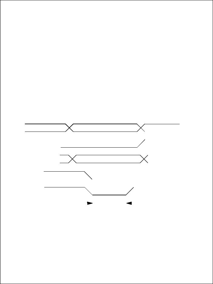
Any message can be illegalized by applying an active low on the NME signal within 600 nSec of the rising edge of NVCR at this time. If NME signal is pulled w,lo the RT will respond with a Status word having the Message Error bit set.
T0-15 |
|
|
|
|
|
CMD WD |
|
|
NVCR |
|
|
|
|
|
|
|
|
NME |
500 nSec |
|
|
|
|
|
|
|
|
|
|
|
|
|
|
||
|
|
|
|
|
|
|
||
|
|
|
|
|
|
|
||
|
|
|
|
|
|
|
|
|
 600 nSec
Max
One way to implement this function is to place a latching PROM to the T0-T10 data bus. The PROM would only have to decode 11 bits (5 bits subaddress, 5 bits word count, 1 bit T/R) and have a one bit output to place a high/low level on the NME input pin. The upper five bits (T11-T15) are just the RemoteTerminal address for the unit which is a constant so no decode of these bits are necessary. The latching signal for the PROM would be the NVCR line. The NME pin will be read and acted upon 600 nSec after the rising edge of NVCR. The NME signal would remain latched and stable until the next rising edge of NVCR.
MIL-STD-1760 FEATURES
To enable the 1760 features checksum validation, the NENCHK line is held wlo. This enables the integrated on-chip hardware checksum features. The hardware automatically checks the incoming message for the correct checksum.
1760 HEADER WORD
The signal NHDR will be an early indicator of the 1760 header word. This headerword will appear on the T0-15 bus when the NHDR signal is low. The NHDR signal will go low on every header word (first data word) even if the 1760 checksum circuitry is enabled or not. NHDR is just an indicator of the first data word on the bus T0-15.
T0-15 |
1760 HDR WD |
NHDR
500 nSec 
APPLICATION NOTE #108 |
9 |
Released 9/98 |
SIGNALS THAT INDICATE CHECKSUMFAILURE
For 1760 applications, the STATUS line indicates if a message has failed checksum. The STATUS line will toggle up or down for each received data word as it is calculating the checksum and is sampled on the falling edge of NCMDSTRB. The TATUSS line can be tied to any of the Status Word Bit inputs to set those bits in the event of a checksum fail.TATUSS
is an open output line that will set the selected Status Word Bits for the Status Word response in the current message. This is one of the great features for this product. The subsystem does not have to verify the checksum in software to detect the err.oThe SmaRT unit automatically does this in hardware and the unit is able to flag the error and set the a Status Word Bit on the CURRENT Status Word response . This minimizes processor overhead and reduces response time in notifying the Bus Controller that an error has occurred.
For 1760 applications, the NVALCHK signal also indicates a valid checksum for the Receive Command message. NVALCHK is a latched version of the STATUS signal and is updated only on Receive Commands. It is valid on the falling edge of NCMDSTRB of a Receive Command and remains stable until the next Receive Command message. ATransmit Command message will not alter this signal because aTransmit Command does not require an incoming checksum validation.
T0-15 |
|
|
|
|
|
CMD WD |
|
|
|
|
|||||||
NEMPTY |
|
|
|
|
|
|
|
|
|
|
|
|
|
|
|
|
|
|
|
|
|
|
|
|
|
|
|
|
|
|
|
|
|
|
|
|
|
|
|
|
|
|
|
|
|
|
|
|
|
|
|
||
STATUS |
|
|
|
|
|
VALID |
|
|
|
|
|
||||||
NVALCHK |
|
|
|
|
|
Latched Until Next Receive Command |
|
|
|
|
|||||||
NCMDSTRB |
|
|
|
|
|
|
|
|
|
|
|
|
|
|
|
|
|
|
|
|
|
|
|
|
|
|
|
|
|
|
|
|
|
|
|
|
8.5 µSec |
|
|
|
|
|
|
|
|
|
|
|
|||||
|
|
|
|
|
|
|
|
|
|
|
|
|
|||||
|
|
|
|
|
|
|
|
|
|
|
|
|
|
|
|
||
|
|
|
|
|
|
|
|
|
|
|
|
|
|
|
|
|
|
BLOCK TRANSFER LOGIC
The Block Transfer Logic (BTL) may be enabled for both RemoteTerminal and Bus Controller.
The BTL consists of a 32 word memory buffering the subsystem to the main RAM thus guaranteeing data consistency for both transmit and receive transfers.
All reads and writes to the BTL are identical to read / write to the main RAM. The address locations are the same. The only difference is that the BTL circuitry will intercept those read
APPLICATION NOTE #108 |
10 |
Released 9/98 |
/ writes and store them in the buffer instead. The user accesses the same locations as if they would if they were directly accessing the main RAM.
The block transfer logic is enabled with signal NENBTL (pin A7) being active low and is not applicable to subaddress 00 and 1F (unless McAir is selected) areas of ram. The block transfer logic may also be configured by writing to certain address locations providing NENBTL is selected, ie.
0 1 00 02 |
402h |
Disable Read |
Disable Write |
||
0 1 00 03 |
403h |
Disable Read |
Enable |
Write |
|
0 1 00 04 |
404h |
Enable |
Read |
Disable Write |
|
0 1 00 05 |
405h |
Enable |
Read |
Enable |
Write |
Reset will enable both Write and Read.
Note: All 257X versions with internal RAM that do not have NENBTL as a dsiscrete input have it enabled internally.
READ (RECEIVE)
The Read BTL functions similarly to the Write BTL in that the BTL buffers the read activity. A subsystem read will initially generate a DMA of that entire portion of the subaddress to be stored in the BTL buffer. The subsystem can then read out the data at its leisure while the main RAM is free for future updates. Since the entire portion of the subaddress data was DMA from the RAM, the data read from the BTL buffer is guaranteed contiguous.
The user must read data from the device in a specific sequence starting with the first word received in the n-1 location and ending with the last word received in location 00 of the subaddress. The BTL will sense the read from location 00 and reset the sequence ready for a new access.
1.The first word of a received message will be read first, this will initiate a burst DMA transfer of a complete message from main memory to the 32 word BTL buffer memory, during which time the subsystem will be locked out. Data is transferred at the rate of 250 ns per word.
2.The sub system can then read data from the ram at its leisure. The last word to be read will be the last word received in the message and read from location zero. This will reset the block transfer logic.
3.If the 1553 DMA transfer to the main RAM becomes active during the burst transfer, the transfer will complete and then be locked out until the 1553 is complete. However the 32 word BTL buffer memory will be accessible to the subsystem at this time to read out the data.
4.If the 1553 DMA transfer to the main RAM becomes active before the start of the burst transfer, the transfer will belocked out until the 1553 is complete. The sub system will be locked out during this time (main ram being accessed by the 1553 and the 32 word buffer memory is waiting for the receive message). When the 1553 is complete the burst transfer will take place and then unlock the subsystem.
APPLICATION NOTE #108 |
11 |
Released 9/98 |

5. Once the burst transfer has commenced it will complete, thus ensuring data consistency.
DMA TRANSFER TIMES
The DMA cycle transfers words from the FIFO to internal RAM at a rate of one word each 1 µSec. The maximum DMA cycle time could possibly occur for a 32 data word transfer if the RAM is accessed at the beginning of NCMDSTRB Strobe. Maximum subsystem hold-off time would be 8.5 µSec (NCMDSTRB Signal) + 32 µSec (0.5 µSec per word) for a total of 24.5 µSec.
TRANSMIT COMMAND
The incoming command word is verified for all protocol checks (such as parity and bit count). The verified command word is placed on the T0-15 bus and the NVCR signal is strobed. It is at this time that a message can be illegalized.
T0-15 |
CMD WD |
NVCR
NME |
500 nSec |
|
|
|
|
|
|
|
|
|
|
|
|
|
|
||
|
|
|
|
|
|
|
||
|
|
|
|
|
|
|
|
|
 600 nSec
Max
Any message can be illegalized by applying an active low on the NME signal within 600 nSec of the rising edge of NVCR at this time. The RT will respond with a Status word having the Message Error bit set. See Section 1.2.1.1 for implementing the Message Illegalization.
The NCMDSTRB goes low indicating that a completely validated message has been received. The validated Command Word again appears on the T0-15 bus at this time. The end of the NCMDSTRB strobe will initiate the DMA cycle to transfer the data words from internal RAM to the buffer FIFO.
Buffering the outgoing message with a FIFO means that the subsystem is allowed the most flexibility to access the RAM without contending with 1553 bus traffic. In 1553, data words are transmitted at a rate of 20 µSec per word or a maximum time of 640 µSec for a 32 word transfer. Many other systems do not buffer the outgoing data at all. That means that the RAM is periodically being accessed for data words from the RAM for up to 640 µSeconds. The SmaRT unit buffers the outgoing data so that the RAM is completely available to the subsystem after the DMA transfer from RAM occurs. The possibilities of memory contention is greatly reduced and the contents of the outgoing data will not be affected by subsystem operations.
The NCMDSTRB pulse is 8.5 µSec long and during this time interval, the bus arbitration logic is active. If the subsystem has already begun a read/write operation before NCMDSTRB, the NACK (acknowledge) signal will go low for 500 nSec allowing the
APPLICATION NOTE #108 |
12 |
Released 9/98 |

completion of the read/write command. The read/write operation must be completed within the remaining 8 µSec. If a read/write operation starts after the NCMDSTRB strobe has begun, the NACK will not occur and thus hold off the subsystem for the duration of the DMA cycle from internal RAM.
During NCMDSTRB, the Command Word is loaded into the Command/Status FIFO stack and the NEMPTY line goes high. The user can utilize this signal as an indication that some activity has occurred. The Command/Status FIFO stores up to 32 command words for the subsystem to review. This allows the processor to only response to the 1553 unit when something has occurred. Constant polling of the 1553 unit is not requiredTo. reduce processor intervention even further, the Command/Status FIFO will only store commands that have associated data with it.
MIL-STD-1760 FEATURES
If the 1760 features are enabled (NENCHK line is held low), the checksum word is automatically generated and transmitted as the last data word. The subsystem processor does not have to calculate or load the checksum word into RAM. The SmaRT unit automatically does this in hardware and transmits the correct checksum data word as the last word out. This reduces subsystem processor overhead significantly.
SIGNALS THAT INDICATE CHECKSUMFAILURE
For 1760 applications, the STATUS line indicates if a message has failed checksum. The TATUSS line will stay high for aTransmit Command word because there is no associated data words received for checksum validation. STATUS is sampled on the falling edge of NCMDSTRB. The TATUSS line can be tied to any of the Status Word Bit inputs to set those bits in the event of a checksum fail. STATUS is an open output line that will set the selected Status Word Bits for the Status Word response in the current message. This is one of the great features for this product. The subsystem does not have to verify the checksum in software to detect the erro.The SmaRT unit automatically does this in hardware and the unit is able to flag the error and set the a Status Word Bit on the CURRENT Status Word response . This minimizes processor overhead and reduces response time in notifying the Bus Controller that an error has occurred.
For 1760 applications, the NVALCHK signal does not change from it's previous state since aTransmit Command Word has no incoming data words. NVALCHK is a latched version of the STATUS signal and is updated only on Receive Commands. It is valid on the falling edge of NCMDSTRB of a Receive Command and remains stable until the next Receive Command message. TransmitA Command message will not alter this signal because aTransmit Command does not require an incoming checksum validation.
T0-15 |
CMD WD |
NCMDSTRB
NEMPTY
NVALCHK |
* * * |
PREVIOUS STATE |
* * * |
8.5 µSec 
APPLICATION NOTE #108 |
13 |
Released 9/98 |
 Loading...