

Page 1
5
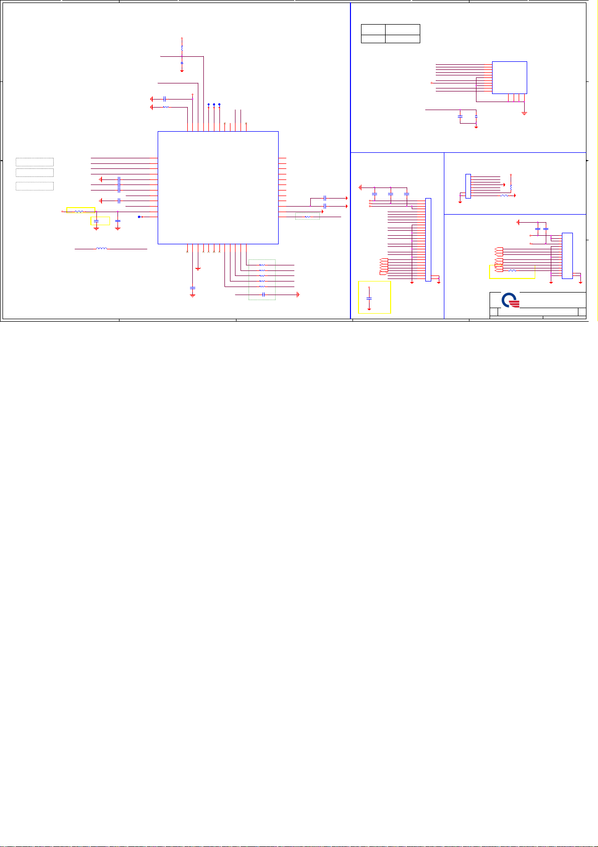
Card reader controller (MMC)
4
3
2
1
2 IN 1 CARD READER (SD/MMC)
PLTRST #
PCIE_C LKREQ0 #
C52 0.1U/10 V_4
R38 6.2K/F_4
U6
1
HSIP
2
HSIN
3
REFCLKP
4
REFCLKN
5
AV12
6
HSOP
7
HSON
8
GND
9
DV12
10
Card1_3V3
11
3V3_IN
12
Card2_3V3
+3V3_IN
R42
*100K_4
C45
*1U/6.3V_4
+3V3_IN
TP8
TP6
TP7
EEDO
EECS
CARDREF
PLTRST#
EESK
42
43
44
45
46
47
48
RREF
EECS
EEDO
3V3_IN
PERST#
CLK_REQ#
RTS5209-GR
XD_CD#13DV33_1814GND15SP116SP217SP318SP419SD_D120SD_D021SD_CLK22SD_CMD23SD_D3
GND
DV33_18
C34
0.1U/10V_ 4
4
SD_WP/XD_D7
SD_CD#
38
39
40
41
EESK
SD_CD#
MS_INS#
GPIO/EEDI
24
SD_D1
SD_D0
SD_CLK
SD_CMD
SD_D3
SD_CLK _R
SP1437SP15
36
SP13
35
SP12
34
SP11
33
SP10
32
SP9
31
SP8
30
SP7
29
SP6
28
SP5
27
DV12_S
DV12_S
26
GND
GND
25
SD_D2
R26 33/J_4
SD_D2
<Layout Note> Place Close to Chip Pin
<Layout Note> Place Close to Chip Pin
R28 33/J_4
SD_D3_ R
SD_CMD_ R
R31 33/J_4
SD_CLK _R
R33 33/J_4
SD_D0_ R
R35 33/J_4
SD_D1_ R
R37 33/J_4
C24 10P/50V_ 4
3
C17 4.7U/6.3 V_6
C18 0.1U/10 V_4
SD_D2_ R
+3VPCU
+3V_S5
CN11
C36
10u/6.3V_ 6
C37
0.1u/16V_ 4
11
CARD/DET
10
W/P
9
DATA2
8
DATA1
7
DATA0
6
VSS2
5
CLK
4
VDD
3
VSS1
2
CMD
1
CD/DATA3
SD-CARD
GND13GND
GND
GND
14
12
15
SD_CD#
SD_WP /XD_D7
SD_D2_ R
SD_D1_ R
SD_D0_ R
SD_CLK _R
VCC_XD
SD_CMD_ R
SD_D3_ R
VCC_XD
Close to CN14 pin 14 & pin23
4.7u CAP close to pin23
TP CN(TP to Board)CR/TP CN
CN6
1
2
3
4
5
6
789
32
10
TP CN
Audio CN
PCH_AZ_ CODEC_ RST#3
PCH_AZ_ CODEC_ SYNC3
PCH_AZ_ CODEC_ SDIN03
PCH_AZ_ CODEC_ SDOUT3
PCH_AZ_ CODEC_ BITCLK3
C5
C7
C8
*0.1U/10V_ 4
*0.1U/10V_ 4
+3V
+TPVDD
TPCLK_ R
TPDATA _R
CLK_SD ATA
CLK_SC LK
PCIE_T X2+
PCIE_T X2-
CLK_PC IE_MMC
CLK_PC IE_MMC#
PCIE_R X2+
PCIE_R X2-
PLTRST #
PCIE_C LKREQ0 #
KEY_BL_ EN3
PWRLE D#2
SUSLED#2
BATLED 1#2
BATLED 0#2
NBSWON#2
TP_INT# _D
BOARD_ ID4
+3V
C69
20120119 For EMI solution.
0.1U/10V_ 4
*0.1U/10V_ 4
2
CN7
1
2
3
4
5
6
7
8
9
10
11
12
13
14
15
16
17
18
19
20
21
22
23
24
25
26
27
28
293031
CON30P
+TPVDD
+TPVDD
TPCLK_ R
TPDATA _R
CLK_SD ATA
CLK_SC LK
TP_INT# _D
BOARD_ ID4
PCBEEP _EC3
AMP_MUTE#3
R6
*4.7K_4
R5 *0_4
LOW=ELAN
HIGH=SYNAPTICS
C10
C11
*0.1U/10V_ 4
*0.1U/10V_ 4
+5V
SPKR3
Size Document Numb er Rev
Size Document Numb er Rev
Size Document Numb er Rev
Date: Sheet of
Date: Sheet of
Date: Sheet of
+3V
PCH_AZ_ CODEC_ BITCLK _R
0_4
R10
20111116 For EMI solution.
Quanta Computer Inc.
Quanta Computer Inc.
Quanta Computer Inc.
PROJECT :
PROJECT :
PROJECT :
RTS5209-GR (Card Reader)
RTS5209-GR (Card Reader)
RTS5209-GR (Card Reader)
1
Z09
Z09
Z09
10
11
12
13
14
15
16
1 1Monday, April 09, 2 012
1 1Monday, April 09, 2 012
1 1Monday, April 09, 2 012
Audo_CO N
1
2
3
4
5
6
7
8
9
1
2
3
4
5
6
7
8
9
10
11
12
13
14
17
15
17
18
16
18
CN5
D D
C C
PCIE_T X2+
Zdiff = 100 ohm
Zdiff = 100 ohm
Zdiff = 100 ohm
20111207 change from 2.2ohm to 0 ohm for SD3.0
B B
huge current
20111117 base on FAE request change to 10U.
A A
+3V
5
R40 *SHORT_8
PCIE_T X2CLK_PC IE_MMC
CLK_PC IE_MMC#
PCIE_R X2+
PCIE_R X2-
C44
10u/6.3V_ 6
AV12
L7 *PBY1608 08T-601 Y-N_1A
C47 4.7U/6.3 V_6
C42 0.1U/10 V_4
C43 0.1U/10 V_4
C41 0.1U/10 V_4
C40
0.1U/10V_ 4
AV12
PCIE_R XP2_C
PCIE_R XN2_C
GND
DV12
VCC_XD
+3V3_IN
TP9
DV12
1D
1D
1D
Page 2
5
R62 *1M_4
Power LED
D D
PWRLED#1
SUSLED#1
R58 *1M_4
R63 300/F_4
R59 560_4
+3V_LED
LED5
1
4
Blue
LED_B/R
4
3
2
1
For LED/cardreader/Power button
+3V_LED
2
3
+3V_LED
R65 *0_6
R66 0_6
+3V_S5
+3VPCU
Amber
R60 *1M_4
R56 *1M_4
Battery
+3VPCU
C68
R61 300/F_4
R57 560_4
R55
10K_4
C67
*1000P/16V/X7R_4
BATLED0#1
C C
B B
A A
BATLED1#1
NBSWON#1
0.1U/10V/X5R_4
5
NBSWON#
*14V/38V/100P_4
+3VPCU
LED6
LED_B/R
+3VPCU
2
3
SW5
12
34
SWITCH
4
PAD4
*spad-z09-1np
1
HOLE7
HOLE6
*h-c196d98p2
1
3
*h-c236d98p2
1
HOLE8
*h-c79d79n
1
Quanta Computer Inc.
Quanta Computer Inc.
Quanta Computer Inc.
PROJECT :
PROJECT :
Size Document Number Rev
Size Document Number Rev
Size Document Number Rev
Date: Sheet of
Date: Sheet of
2
Date: Sheet of
PROJECT :
LED
LED
LED
Z09
Z09
Z09
2 2Monday, April 09, 2012
2 2Monday, April 09, 2012
2 2Monday, April 09, 2012
1
1D
1D
1D
Blue
1
4
Amber
12
D10
Page 3

Codec(ADO)
5
ADOGND
Place near codec
C35
D D
+5VA
ADOGND
Place next to pin 38
+5V
C23
10u/6.3V_6
+5V
C22
10u/6.3V_6
C C
C28
10u/6.3V_6
C3C
R36 0_6
C21
0.1u/10V_4
Place next to pin 39
C3C
R34 0_6
C20
0.1u/10V_4
Place next to pin 46
C29
0.1u/10V_4
ANALOG
Spilt by AGND
+5VPVDD1
C25
C26
10u/6.3V_6
0.1u/10V_4
Spilt by PGND
+5VPVDD2
C27
C30
Spilt by DGND
10u/6.3V_6
0.1u/10V_4
C3C
R41 2.2/F_6
+3V
0V : Power down Class D SPK amplifer
3.3V : Power up Class D SPK amplifer
C32
+
2.2u/6.3V_6
U7
ADOGND
37
AVSS2
38
AVDD2
39
PVDD1
40
L_SPK+
SPK-L+
41
L_SPK-
SPK-L-
42
PVSS1
43
PVSS2
44
R_SPK-
SPK-R-
45
R_SPK+
SPK-R+
46
PVDD2
47
EAPD#
SPDIFO2/EAPD
48
SPDIFO
49
PGND
+AZA_VDD
C31
0.1u/10V_4
Place next to pin 1
DMIC_DAT_L
DMIC_CLK_L
PD#
2.2u/6.3V_6
36
CBP
(Vista Premium Version)
DVDD11GPIO0/DMIC-DATA2GPIO1/DMIC-CLK3PD#4SDATA-OUT5BIT-CLK6DVSS27SDATA-IN8DVDD-IO9SYNC10RESET#11PCBEEP
C33
10u/6.3V_6
4
HPR
HPL
MIC1-VREFO-L
TP10
MIC1-VREFO-R
TP11
MIC2-VREFO
C6461 place near to codec
IN_MIC-VREFO
C39 10u/6.3V_6 R17
ADOGND
26
27
28
29
VREF
AVSS1
LDO-CAP
MIC2-VREFO
PCH_AZ_CODEC_RST#
ACZ_SDIN
R39 33/J_4
C38 *22p/50V_4
Place next to pin 27
C50
2.2U/6.3V_6
25
AVDD1
LINE1-R
LINE1-L
MIC1-R
MIC1-L
MONO-OUT
JDREF
Sense-B
MIC2-R
MIC2-L
LINE2-R
LINE2-L
Sense A
ALC271X
12
DIGITAL
+
30
31
32
33
34
35
CBN
CPVEE
HP-OUT-L
HP-OUT-R
MIC1-VREFO-L
MIC1-VREFO-R
ADOGND
C49
C51
+
0.1u/10V_4
*2.2u/10V_4
0.1u/10V_4
24
23
22
21
20
19
18
17
16
15
14
13
Place next to pin 25
MIC1_R1
TP12
MIC1_L1
TP13
R47 20K/F_4
SENSEB MIC2-JD#
MIC2_R2
MIC2_L2
SENSEA
R46 20K/F_4
TP15
TP14
R48 39.2K/F_4
ADOGND
ANALOG
PCBEEP dont coupling any signals if possible
8/17 separate PCBEEP to Digital from Realtek suggestion
1.6Vrms
BEEP_1PCBEEP
C54 1u/10V_6
C53
R45
4.7K_4
100p/50V_4
PCH_AZ_CODEC_RST# 1
PCH_AZ_CODEC_SYNC 1
PCH_AZ_CODEC_SDIN0 1
PCH_AZ_CODEC_SDOUT 1
PCH_AZ_CODEC_BITCLK 1
R43 47K_4
3
+5VA
C56
C55
10u/6.3V_6
ADOGND
Close to codec
<20110823>co-lay ALC281x
R6128 un-stuff.
HP_JD#
D9
BAT54C
If either HDA device io power use +1.5V,
all device IO power change to +1.5V
C46
0.1u/10V_4
5/4 add
C48
10u/6.3V_6
PCBEEP_EC 1
SPKR 1
+AZA_VDD
C-test
Place next to pin 9
HEADPHONE/Mic combo
2
Change R11,R21 From 75 ohm to 47 ohm for FAE suggestion.
HP-L-2
HP-R-2
R21 47/J_4
R11 47/J_4
COMBO_MIC
EAPD#
COMBO_MIC
ADOGND
HPR-1
R9
*1K/J_4
MIC2-VREFO
R24
2.2K/J_4
R25 1K/J_4
R16
22K/F_4
R27 *0_4
R23 22K/F_4
L6 *SHORT_6
L5 *SHORT_6
*1K/J_4
C19
10U/6.3V_8
ADOGND
DMIC Conn
C15
C12
2200P/50V_4
2200P/50V_4
ADOGND
C59 2.2U/6.3V_6
C58 2.2U/6.3V_6
<20100917> Add 22k PD by FAE
suggestion for discharing
2
RF suggest to add R144,R149,C118,C134
Reserve for DMIC.(not use)
MIC2_R2
MIC2_L2
MIC2-JD#
3
Q6
2SK3018
1
<20110823>co-lay ALC821x
Q5047 un-stuff.
R8 stuff.
Close to codec
R54
BLM15AG601SS1D(600,0.3A)
R53
C66
*150p/50V_4
BLM15AG601SS1D(600,0.3A)
C65
*150p/50V_4
1
Swap CN10 pin3 pin4 for SIT wrong SPEC issue.
DMIC_DATDMIC_DAT_L
DMIC_CLKDMIC_CLK_L
HPL_SYSHPL-1
HPR_SYS
12
ADOGND
HP_JD#
14V/38V/100P_4
COMBO_MIC
D5
+3V
COMBO_MIC
12
D11
EGA10402V05AH(0402)
If audio jack is normral Open
Q5048/R6129 should be remove,
directly link HP_JD#.
If normral Close stuff Q5048/R6129.
20110909 del Q5048,R6129
CN9
1
2
5
3
6
4
MIC-CONN
20111207 change to DFHS04FRC51
3
4
1
2
5
6
2SJ3005-017111F-CUS
CN10
Close to conn
Keyboard LED control
B B
KEY_BL_EN1
Power (ADO)
+5V
A A
C60
C64
*10U/10V_8
*0.1u/10V_4
C730, C787 close U37 pin3 and L58
+5V+5V
1
R7133
10K/J_4
KB_LED#
2
Q7015
DDTC144EUA
1 3
ANALOG DIGITAL
L8 TI201209U310N001/6A/31ohm_8
U8
4
3
OUT
IN
2
GND
5
1
SET
SHDN
*G923-330T1UF
R52 *0_4
5
ADOGND
Q7013
AO3413
2
R51 *29.4K/F_4
R49
*10K/F_4
20mil
3
KB_LED_PWR
C7286
C7284
0.01U/25V_4
*10U/6.3V_6
CN12
KB_LED
4
3
2
6
1
5
ON/OFF only
Mute(ADO)
*10U/10V_8
+5VA
C63
C62
*0.1u/10V_4
ADOGND
+5V
R30
*10K_4
4
R22 *0_4
PCH_AZ_CODEC_RST#PD#
D8BAS316
EAPD#
D7*BAS316
D6BAS316
AMP_MUTE# 1
R12 0_4
R32 0_4
R13 0_4
R50 0_4
R44 0_4
R29 0_4
C61 *1000p/50V_4
C57 *1000p/50V_4
ADOGND
3
Hp Mute
AMP_MUTE#1
Internal Speaker
40mil for each signal
R_SPK+
R_SPK-
L_SPK+ L_SPK+_1
Q5 unmunt for FAE suggestion.
(if we use, it will cause bobo noise)
+5V
53
U5
1
4
R14 *0_4
2
EAPD#
*TC7SH08FU
Change CN8 footprint from 88231-0400-4p-r to
1775295-4-4p-l for PDC speak pindefine rule.
R18 *SHORT_6
R15 *SHORT_6
R7 *SHORT_6
R8 *SHORT_6
2
C16
*68p/50V_6
C13
*68p/50V_6
HP_MUTE#
HPL
HPR
C14
*4.7u/10V_6
C6
*68p/50V_6
R_SPK+_1
R_SPK-_1
L_SPK-_1L_SPK-
*68p/50V_6
HP_MUTE#
C9
*SHORT_4
HP-R-2HP-R-2
HP-L-2HP-L-2
SPEAKER-CONN
4
3
6
2
5
1
CN8
Size Document Number Rev
Size Document Number Rev
Size Document Number Rev
AUO/AMP
AUO/AMP
AUO/AMP
Date: Sheet of
Monday, April 09, 2012
Date: Sheet of
Monday, April 09, 2012
Date: Sheet of
Monday, April 09, 2012
6
R19
215
4 3
Q5
*2N7002DW
Quanta Computer Inc.
Quanta Computer Inc.
Quanta Computer Inc.
PROJECT :
Z09
PROJECT :
Z09
PROJECT :
Z09
1
R20
*SHORT_4
33
33
33
1D
1D
1D
Page 4

5
Model
Z09
D D
C C
REV
3.23
FIRST RELEASED
1. Page2 modify LED only Power and Battery indicator.
A1A
2. Page1 modify connector pin define.
3. Page1 Change R5948 from 0ohm to 2.2ohm to prevent ESD issue.
4. Page1 Change CN17 from 24pin to 30pin add TP con and Audio connector.
5. Page3 Add codec.
6. Page1 CN9 of BITCLK pin reserve 0ohm and CAP for EMI request.
7. Page1change C5156/C6158 to 10U.
8. Page1 Add CN17 pin for Batt_EN#, and add short point.
9. Add Hp Mute function
10. CN7 change to 8 pin
11. Add net TP_INT_D
11. Change net TP_INT_D to TP_INT#_D
12. Add pull high resistor on net TP_INT#_D
13. Add 0 ohm on CN7 pin8
14. Add screw hole
15. Mirror CN17
16. Mirror CN9
17. Change CN5012 pin define
18. Change CN5014 pin define
19. Change CN14 type and pin define
20. Change screw hole symbol 2011/11/30
21. Change Card reader symbol 2011/11/30
22. Change JP6005 footprint 2011/12/1
23. Change R6132 from 0ohm to 2.2ohm for ESD
24. Change SW6 symbol and footprint
25. Add screw hole 2011/12/1
26. Change C6148 form 4.7u to 10u for FAE suggestion 2011/12/2
27. Change CN14 footprint 2011/12/2
28. Correct Mute function 2011/12/6
29. Change MIC conn type to DFHS04FRC51 2011/12/7
30. For SD/MMC , R5947 and C6147 useless, delete it. 2011/12/7
31. Delete C6158 for FAE suggetion. 2011/12/7
32. Change from 2.2ohm to 0 ohm for SD3.0 huge current 2011/12/7
33. Change screw hole type 2011/12/7
34. Delete TP5060
35. update screw hole name
36.Rename 2011/12/9
37.Delete JP6005, add TP9 2011/12/9
38.Add pad1,pad2 for EMI 2011/12/9
4
CHANGE LIST
2011/11/29
2011/11/29
2011/11/30
2011/11/30
2011/11/30
2011/11/30
2011/11/30
2011/11/30
2011/12/1
2011/12/1
2011/12/7
2011/12/7
3
2
MODEL
1
Z09
FROM To
39.Swap LED GPIO setting for wrong color issue.
A1B
40.Swap CN10 pin3 pin4 for SIT wrong SPEC issue.
41.Q5 unmunt for FAE suggestion.(if we use, it will cause bobo noise)
42.Change CN8 footprint from 88231-0400-4p-r to 1775295-4-4p-l for PDC speak pindefine rule.
43.Add Varistor on MIC signal.
44.Modify CN10 Symbol
45.Add C69 for EMI
46.Add PAD4 for EMI
B B
A A
48.R57,R59 change from 100 ohm to 680 ohm for adjust LED brightness 2012/02/01
C1A
49.Change R11,R21 From 75 ohm to 47 ohm for FAE suggestion.
50.Change CN6 PN from DFFC08FR007 to DFFC08FR035
51.Add Keyboard backlight control sch. 2012/02/07
52.Change C60,C63 footprint from 3216 to 0805 2012/02/13
53.Update CN12 PN from DFFC04FR014 to DFFC04FR070 2012/02/20
54.Add R64 0 ohm and modify CN12 pin define for Darfon keyboard 2012/02/21
55.Modify CN12 symbol 2012/02/22
56.Add R65,R66 for DS3 LED flash 2012/02/22
57.Modify CN12 pin define 2012/02/24
58.Reserve 0 ohm neer by CN12 for Darfon keyboard 2012/02/24
59.Change R57,R59 from 680 ohm to 560 ohm for adjust LED brightness 2012/02/25
60.Modify CN6 pindefine for touchpad 2012/03/02
C1B
61.Modify CN6 CN7 pindefine for touchpad 2012/03/05
62.Modify CN6 pin7,Pin8
63.Remove R67,R68,R69,R70 2012/03/12
64.Delete Pad1,change hole8 type. 2012/03/21
65.Delete Pad3 2012/03/21
66.Change CN8,CN9 PN for SMT request (add mylar). 2012/03/22
67.Change L5,L6,R7,R8,R15,R18 to shortpad0603,R19,R20 to shortpad0402,R40 to shortpad0805 2012/03/30
68.C51 change form 0603 to 0402 2012/03/30
2012/01/16
2012/01/16
2012/01/16
2012/01/16
2012/01/19
2012/01/19
2012/01/19
2012/01/19
2012/01/1947.Delete PAD2 for EMI
2012/02/06
2012/02/06
2012/03/09
B2B
Quanta Computer Inc.
Quanta Computer Inc.
Quanta Computer Inc.
PROJECT :
PROJECT :
Size Document Number Rev
Size Document Number Rev
Size Document Number Rev
Date: Sheet of
Date: Sheet of
Date: Sheet of
PROJECT :
Change list
Change list
Change list
Z09
Z09
Z09
4 4Monday, April 09, 2012
4 4Monday, April 09, 2012
5
4 4Monday, April 09, 2012
DOC NO.
1B
1B
1B
4
PART NUMBER:
3
APPROVED BY:PROJECT MODEL : Z09
DRAWING BY: REVISON:
2
DATE:
2010/7/20
1A
1
 Loading...