Acer ACERPOWER PRO Annexe 1

& K DSWHU
System Board
The V60N is a high-performance system board with a 64-bit
architecture. It supports the new Intel Pentium Pro CPU running at
150/166/180/200 MHz and utilizes the Peripheral Component
Interconnect (PCI) local bus architecture. The PCI local bus
maximizes the system performance by enabling high-speed
peripherals to match the speed of the microproces sor with its 120 MB
or 132 MB per second transfer rate in burst mode.
The board comes with four ISA and four PCI slots for future
expansion. The six 72-pin SIMM soc k ets allow you to upgrade system
memory to a maximum of 384 MB.
Onboard I/O interfaces comprise of two UART 16C550 serial ports, a
parallel port with ECP/EPP feature, and PS/2 keyboard and mouse
ports. These allow the system to support various I/O devices.
System Board 1-1

1.1 Major Features
The system board has the following major features and components:
A zero-insertion force (ZIF) socket for Intel Pentium Pro CPU
•
series
Six 72-pin SIMM sockets that suppor t 4-/8-/16-/32-/64-MB, 60-ns
•
SIMMs, with Extended Data Out (EDO) or Fast Page Mode (FPM)
feature
128-KB Flash ROM
•
APM-compliant BIOS
•
Onboard PCI local IDE controller
•
Two PCI-enhanced IDE interfaces that support up to four IDE
•
devices
SCSI and Ethernet function interface (optional)
•
External ports:
•
PS/2 keyboard and mouse ports
•
Two buffered high-speed serial ports
•
One ECP/EPP high-speed parallel port
•
1-2 User’s Guide

1.2 Board Layout
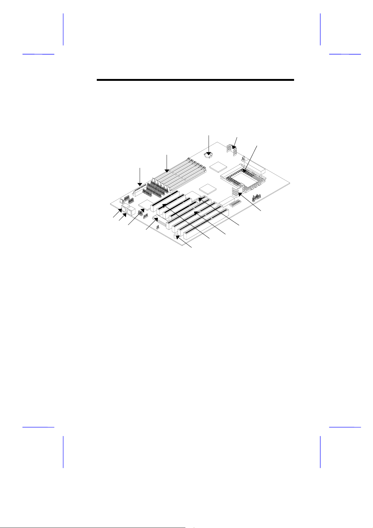
Figure 1-1 shows the locations of the system board major
components.
2
1
14
13
12
11
10
1 Power connector
2 SIMM sockets
3 Battery
4 1.5V voltage regulator with heatsink
5 CPU socket
6 3.3V voltage regulator with heatsink
7 SCSI/LAN card slot
8 ISA slots
9 PCI slots
3
4
5
6
7
8
9
10 Buzzer
11 BIOS chip socket
12 Ultra I/O controller
13 PS/2 mouse connector
14 PS/2 keyboard connector
Figure 1-1 System Board Layout
System Board 1-3

1.3 Jumpers and Connectors
1.3.1 Jumper and Connector Locations
Figure 1-2 shows the jumper and connector locations on the s ystem
board.
Figure 1-2 System Board Jumper and Connector Locations
The blackened pin of a jumper or a connector
represents pin 1.
1-4 User’s Guide

1.3.2 Jumper Settings
Table 1-1 lists the system board jumpers with their corresponding
settings and functions.
Table 1-1 Jumper Settings
Jumper Setting Function
Password Check
JP1 1-2
Flash ROM Type
JP4 1-2
Frequency Select
JP5
*
2-3
*
2-3
Switch No.
1 2 3 4 Frequency
On Off Off Off 60MHz
Off On Off Off 66MHz
Check password
Bypass password
128-KB Flash ROM
256-KB Flash ROM
Core/Bus Clk. Ratio
5 6 7 8 Ratio
On On On On 2
On On Off On 3
On On On Off 4
On On Off Off 5
On Of f On On 5/2
On Of f Off On 7/2
On Of f On Off 9/2
On Of f Off Off 11/2
* Default
System Board 1-5

Table 1-1 Jumper Settings (continued)
Jumper Setting Function
Voltage Setting
JP9, JP10,
JP12, JP13
Switch Function
JP11 1-3
S/W Shutdown/
Power Function
JP14 1-2
BIOS Voltage
JP15 1-2
JP9 JP10 JP12 JP13 Voltage
2-3 2-3 2-3 2-3 3.5V
2-3 2-3 1-2 2-3 3.4V
2-3 2-3 2-3 1-2 3.3V
1-2 1-2 2-3 2-3 3.2V
2-3 2-3 1-2 1-2 3.1V
1-2 2-3 2-3 2-3 3.0V
1-2 2-3 1-2 2-3 2.9V
1-2 2-3 2-3 1-2 2.8V
2-3 1-2 2-3 2-3 2.7V
1-2 2-3 1-2 1-2 2.6V
2-3 1-2 1-2 1-2 2.5V
External SMI
2-4
2-3
2-3
Reset
Software Shutdown Power
Normal
12V
5V
1-6 User’s Guide

1.3.3 Connector Functions
Table 1-2 lists the differ ent connectors on the system board and their
respective functions.
Table 1-2 Onboard Connectors
Connector Function
CN1 Software shutdown power connector
CN2 COM1 connector
CN3 IDE1 connector
CN4 IDE2 connector
CN5 COM2 connector
CN6 Parallel connector
CN7 Diskette drive connector
CN9 Infrared (IrDA) connector
CN10 HDD LED connector
CN11 Reset key
CO1 Power connector
CNY1 USB connector
JP2 Two-pin fan connector
JP6 Software power key
JP7 Speed LED
JP8 Power LED
System Board 1-7
 Loading...